WO2024127902A1 - 電波反射装置 - Google Patents
電波反射装置 Download PDFInfo
- Publication number
- WO2024127902A1 WO2024127902A1 PCT/JP2023/041266 JP2023041266W WO2024127902A1 WO 2024127902 A1 WO2024127902 A1 WO 2024127902A1 JP 2023041266 W JP2023041266 W JP 2023041266W WO 2024127902 A1 WO2024127902 A1 WO 2024127902A1
- Authority
- WO
- WIPO (PCT)
- Prior art keywords
- patch electrode
- radio wave
- electrode
- strip wiring
- patch
- Prior art date
- Legal status (The legal status is an assumption and is not a legal conclusion. Google has not performed a legal analysis and makes no representation as to the accuracy of the status listed.)
- Ceased
Links
Images


Classifications
-
- H—ELECTRICITY
- H01—ELECTRIC ELEMENTS
- H01Q—ANTENNAS, i.e. RADIO AERIALS
- H01Q3/00—Arrangements for changing or varying the orientation or the shape of the directional pattern of the waves radiated from an antenna or antenna system
- H01Q3/44—Arrangements for changing or varying the orientation or the shape of the directional pattern of the waves radiated from an antenna or antenna system varying the electric or magnetic characteristics of reflecting, refracting, or diffracting devices associated with the radiating element
- H01Q3/46—Active lenses or reflecting arrays
-
- H—ELECTRICITY
- H01—ELECTRIC ELEMENTS
- H01Q—ANTENNAS, i.e. RADIO AERIALS
- H01Q15/00—Devices for reflection, refraction, diffraction or polarisation of waves radiated from an antenna, e.g. quasi-optical devices
- H01Q15/14—Reflecting surfaces; Equivalent structures
-
- H—ELECTRICITY
- H01—ELECTRIC ELEMENTS
- H01Q—ANTENNAS, i.e. RADIO AERIALS
- H01Q15/00—Devices for reflection, refraction, diffraction or polarisation of waves radiated from an antenna, e.g. quasi-optical devices
- H01Q15/14—Reflecting surfaces; Equivalent structures
- H01Q15/148—Reflecting surfaces; Equivalent structures with means for varying the reflecting properties
-
- H—ELECTRICITY
- H01—ELECTRIC ELEMENTS
- H01Q—ANTENNAS, i.e. RADIO AERIALS
- H01Q19/00—Combinations of primary active antenna elements and units with secondary devices, e.g. with quasi-optical devices, for giving the antenna a desired directional characteristic
- H01Q19/10—Combinations of primary active antenna elements and units with secondary devices, e.g. with quasi-optical devices, for giving the antenna a desired directional characteristic using reflecting surfaces
-
- H—ELECTRICITY
- H01—ELECTRIC ELEMENTS
- H01Q—ANTENNAS, i.e. RADIO AERIALS
- H01Q3/00—Arrangements for changing or varying the orientation or the shape of the directional pattern of the waves radiated from an antenna or antenna system
- H01Q3/44—Arrangements for changing or varying the orientation or the shape of the directional pattern of the waves radiated from an antenna or antenna system varying the electric or magnetic characteristics of reflecting, refracting, or diffracting devices associated with the radiating element
-
- H—ELECTRICITY
- H01—ELECTRIC ELEMENTS
- H01Q—ANTENNAS, i.e. RADIO AERIALS
- H01Q9/00—Electrically-short antennas having dimensions not more than twice the operating wavelength and consisting of conductive active radiating elements
- H01Q9/04—Resonant antennas
- H01Q9/0407—Substantially flat resonant element parallel to ground plane, e.g. patch antenna
Definitions
- One embodiment of the present invention relates to the structure of a radio wave reflecting device that uses liquid crystal.
- a phased array antenna controls the directivity of an antenna by adjusting the amplitude and phase of a high-frequency signal applied to each of multiple antenna elements arranged in a plane.
- Phased array antennas use phase shifters to control the phase of the high-frequency signal.
- a phased array antenna device has been disclosed that uses a phase shifter that utilizes the phenomenon in which the dielectric constant of liquid crystal changes with applied voltage (see Patent Document 1).
- radio wave reflecting devices are known that use liquid crystal to control the direction of radio wave reflection, similar to phased array antennas.
- a radio wave reflector has been disclosed in which a metasurface that reflects radio waves is formed by a microstrip patch array sandwiching a liquid crystal layer (see Patent Document 2).
- the radio wave reflecting device disclosed in Patent Document 2 has a structure in which a liquid crystal layer is provided between a patch electrode and an opposing electrode. The direction in which the radio wave reflecting device reflects radio waves is controlled by the voltage applied to the patch electrode. Strip wiring is connected to the patch electrode to apply a bias voltage. However, connecting the strip wiring to the patch electrode can cause a decrease in reflection characteristics, which is problematic.
- One embodiment of the present invention aims to provide a radio wave reflection device that can maintain good radio wave reflection characteristics.
- the radio wave reflection device has a first substrate including a patch electrode, a strip wiring connected to the patch electrode, and a transistor electrically connected to the strip wiring, a second substrate including an opposing electrode facing the patch electrode, and a liquid crystal layer between the first substrate and the second substrate, one end of the strip wiring being connected to the midpoint of one side of the patch electrode, and the other end of the strip wiring being electrically connected to the transistor.
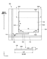
- 1 is a plan view showing a unit cell constituting a radio wave reflecting device according to an embodiment of the present invention
- 1 is a cross-sectional view showing a unit cell constituting a radio wave reflecting device according to an embodiment of the present invention.
- 1 is a plan view showing a unit cell constituting a radio wave reflecting device according to an embodiment of the present invention
- 1 is a plan view showing a configuration of a radio wave reflecting device according to an embodiment of the present invention
- 1 is a cross-sectional view showing a configuration of a radio wave reflecting device according to an embodiment of the present invention.
- 13A and 13B are plan views showing the structure of unit cells having different connection positions of strip wiring.
- FIG. 1A shows a plan view of a unit cell 101 constituting a radio wave reflecting device according to this embodiment, as seen from the front (the surface on which radio waves are incident).
- FIG. 1B shows a vertical cross-sectional view corresponding to line A-B shown in FIG. 1A.
- the unit cell 101 includes a patch electrode 102, a counter electrode 104 (also called a "ground electrode") arranged on the back surface of the patch electrode 102, a liquid crystal layer 110 between the patch electrode 102 and the counter electrode 104, and a transistor 108.
- the patch electrode 102 is provided on a first substrate 150
- the counter electrode 104 is provided on a second substrate 152.
- a first alignment film 112A is provided on the first substrate 150 so as to cover the patch electrode 102
- a second alignment film 112B is provided on the second substrate 152 so as to cover the counter electrode 104.
- the first substrate 150 and the second substrate 152 are arranged such that the patch electrode 102 and the counter electrode 104 face each other with a gap between them.
- a liquid crystal layer 110 is provided so as to fill the gap between the first substrate 150 and the second substrate 152.
- the transistor 108 is connected to a control signal line 114 and a selection signal line 116 provided on the first substrate 150.
- the first substrate 150 and the second substrate 152 are attached to each other with a sealant.
- the distance (cell gap) between the first substrate 150 and the second substrate 152 is 20 to 100 ⁇ m, and is, for example, 50 ⁇ m.
- a spacer may be provided between the first substrate 150 and the second substrate 152 to keep the distance constant.
- FIG. 1A shows an example in which the patch electrode 102 is a square.
- the shape of the patch electrode 102 in a planar view may be a rectangle, a circle, an ellipse, or a polygon with more corners than a square.
- the patch electrode 102 may have a rectangular shape in which some of the corners are cut out.
- the patch electrode 102 has a first side 1021 and a third side 1023 in the same direction as the first direction (in other words, parallel or approximately parallel), and a second side 1022 and a fourth side 1024 in the same direction as the second direction (in other words, parallel or approximately parallel).
- the lengths of these sides are appropriately set according to the frequency (wavelength) of the radio waves applied to the radio wave reflecting device.
- the shape of the patch electrode 102 does not have to be square, but may have a rectangular shape in which the lengths of the first side 1021 and the third side 1023 and the lengths of the second side 1022 and the fourth side 1024 are different.
- the first direction refers to the direction along the Y axis shown in FIG. 1A
- the second direction refers to the direction along the X axis shown in FIG. 1A. Therefore, the first direction and the second direction are in an intersecting (preferably perpendicular or nearly perpendicular) relationship.
- the counter electrode 104 has a larger area than the patch electrode 102 and is provided on the second substrate 152.
- materials that form the patch electrode 102 and the counter electrode 104 can be used.
- the control signal line 114 extends along a first direction, and the selection signal line 116 extends along a second direction.
- the transistor 108 is, for example, a thin-film transistor. There is no limitation on the structure of the transistor 108, and various structures such as a top-gate type or a bottom-gate type can be applied. In FIG. 1A, the transistor 108 is represented by a circuit symbol.
- Transistor 108 has a control terminal (gate), a first input/output terminal (one of the source and drain), and a second input/output terminal (the other of the source and drain).
- the control terminal (gate) of transistor 108 is electrically connected to selection signal line 116, the first terminal (one of the source and drain) is connected to control signal line 114, and the second terminal (the other of the source and drain) is connected to strip wiring 106.
- the strip wiring 106 is formed of a thin conductive pattern extending from the patch electrode 102.
- FIG. 1A shows a structure in which one end of the strip wiring 106 is connected to the second side 1022 of the patch electrode 102, and the other end is connected to the transistor 108.
- the strip wiring 106 includes an extraction portion 1061 extending in a first direction from a connection portion with the patch electrode 102, and an extension portion 1062 bending from the extraction portion 1061 and extending along a second direction.
- the strip wiring 106 is electrically connected to the transistor 108 at the end of the extension portion 1062.
- the transistor 108 is disposed near the portion where the control signal line 114 and the selection signal line 116 intersect. If the length of the extraction portion 1061 of the strip wiring 106 is Ls1 and the length of the extension portion 1062 is Ls2, the lengths of these two portions have a relationship of Ls1 ⁇ Ls2.
- a control signal that controls the alignment state of the liquid crystal molecules in the liquid crystal layer 110 is applied to the control signal line 114, and a selection signal that switches the transistor 108 to an on or off state is applied to the selection signal line 116.
- a selection signal that switches the transistor 108 to an on or off state is applied to the selection signal line 116.
- the control signal applied to the patch electrode 102 is a DC voltage signal or a polarity inversion signal in which a positive DC voltage and a negative DC voltage are alternately inverted.
- the opposing electrode 104 is either grounded or has an intermediate level voltage of the polarity inversion signal applied to it.
- Application of the control signal to the patch electrode 102 changes the orientation state of the liquid crystal molecules contained in the liquid crystal layer 110.
- a liquid crystal material having dielectric anisotropy is used for the liquid crystal layer 110.
- nematic liquid crystal, smectic liquid crystal, cholesteric liquid crystal, or discotic liquid crystal is used for the liquid crystal layer 110.
- the liquid crystal layer 110 has dielectric anisotropy, and the dielectric constant changes depending on the orientation state of the liquid crystal molecules.
- the radio wave reflection device changes the dielectric constant of the liquid crystal layer 110 individually by applying control signals to multiple patch electrodes 102 arranged in a matrix, thereby changing the phase of the reflected wave and controlling the direction of the reflected wave.
- the frequency bands of radio waves reflected by the radio wave reflecting device are the very high frequency (VHF) band, the ultra-high frequency (UHF) band, the super high frequency (SHF) band, the submillimeter wave (THF) band, the extra high frequency (EHF) band, and the terahertz wave band.
- VHF very high frequency
- UHF ultra-high frequency
- SHF super high frequency
- THF submillimeter wave
- EHF extra high frequency
- terahertz wave band The liquid crystal molecules in the liquid crystal layer 110 change their orientation in response to a control signal applied to the patch electrode 102. However, they hardly follow the frequency of the radio waves incident on the patch electrode 102. Therefore, the radio wave reflecting device can control the direction of travel of the reflected wave without being affected by the radio waves.
- the radio wave reflecting device has unit cells 101 arranged in a matrix, and has the function of reflecting linearly polarized waves (vertically polarized waves and horizontally polarized waves) and circularly polarized waves and controlling the direction of travel of the reflected waves.
- FIG. 1A shows a case where the vibration direction of the incident linearly polarized waves is the same direction as the first direction (in other words, parallel or approximately parallel direction) (vertically polarized wave). As shown in FIG.
- the first side 1021 and the third side 1023 of the patch electrode 102 extend along the same direction (or parallel or approximately parallel) with respect to the vibration direction of the vertical polarization, and the second side 1022 and the fourth side 1024 are in a crossing relationship (preferably perpendicular or approximately perpendicular).
- the lead-out portion 1061 of the strip wiring 106 is in the same direction as the vibration direction of the vertical polarization (in other words, parallel or approximately parallel direction), and the extension portion 1062 crosses (preferably perpendicular or approximately perpendicular) the vibration direction of the vertical polarization.
- FIG. 1A shows a schematic diagram of a state in which high current density regions 1601 and 1602 are generated near the first side 1021 and the third side 1023. In the high current density regions 1601 and 1602, the current Ip flows in the same direction as the first direction (in other words, parallel or approximately parallel).
- FIG. 5 shows a reference example of a unit cell 301, and shows an example in which the connection position of the strip wiring 306 is different from that of the unit cell 101 shown in FIG. 1A.
- the strip wiring 306 is connected to the end of the second side 1022 of the patch electrode 102.
- the strip wiring 306 is connected to the second side 1022 so as to be directly connected to the high current density region 1601. Therefore, the current Ip of the high current density region 1601 flows directly into the strip wiring 306.
- the strength of the reflected vertically polarized wave is reduced compared to the vertically polarized wave incident on the unit cell 301.
- Table 1 shows the main polarization and cross polarization reception power difference with respect to the liquid crystal applied voltage for the radio wave reflecting device (where the strip wiring is connected to the center of one side of the patch electrode) configured with the unit cell 101 according to the present embodiment as shown in FIG. 1A and the radio wave reflecting device configured with the unit cell 301 shown as a reference example in FIG. 5.
- the radio wave reflecting device shown in FIG. 5 has a structure in which the connection part of the strip wiring is provided at the end of the patch electrode.
- the liquid crystal applied voltage V0 indicates the case of 0 V
- V1 indicates the case of a voltage higher than V0. Note that this measurement was performed by irradiating the radio wave reflecting device with radio waves and detecting the intensity of the reflected wave with a receiver.
- the radio wave reflecting device configured with the unit cell 301 a tendency was observed in which the main polarization and cross polarization reception power difference became smaller depending on the liquid crystal applied voltage. This is thought to be due to the increase in the reception power of unnecessary cross polarization depending on the liquid crystal applied voltage, and it is understood that the reflection characteristics of the radio wave reflecting device are deteriorated.
- the radio wave reflecting device configured with the unit cell 101 no significant change was observed in the main polarization and cross polarization reception power difference regardless of the liquid crystal applied voltage. This is believed to be because the generation of unnecessary cross-polarized waves is suppressed, and it is understood that good reflection characteristics are obtained.
- connection portion of the strip wiring 106 to the patch electrode 102 is located near the center of the second side 1022 that intersects (preferably perpendicular or nearly perpendicular) with the vibration direction of the vertically polarized wave, and is located in a position where current does not flow directly from the high current density areas 1601, 1602.
- This configuration makes it possible to prevent a decrease in the current generated by the vertically polarized wave, suppresses the attenuation of the reflected vertically polarized wave relative to the incident vertically polarized wave, and obtains good reflection characteristics.
- connection point between the patch electrode 102 and the strip wiring 106 is preferably located away from the high current density areas 1601, 1602, and taking into consideration the position of the transistor 108, it is preferably the midpoint of the second side 1022 of the patch electrode 102.
- the same effect can be expected even if the connection position of the strip wiring 106 is slightly away from the midpoint of the second side 1022 of the patch electrode 102.
- the same effect can be expected if the connection position of the strip wiring 106 is located at a position a length DXL away from the end of the second side 1022 of the patch electrode 102. It is preferable that the length DXL is about one-quarter to one-fifth of the total length XL of the second side 1022 of the patch electrode 102.
- FIG. 2 shows a case where horizontally polarized waves are incident in a configuration similar to the unit cell 101 shown in FIG. 1A. In other words, it shows a case where the vibration direction of the polarized wave incident on the patch electrode 102 is in the same direction as the second direction (in other words, parallel or approximately parallel). In this case, regions 1603 and 1604 of high current density are generated near the second side 1022 and fourth side 1024 of the patch electrode 102.
- the strip wiring 106 is connected to the center of the second side 1022 of the patch electrode 102. As shown in FIG. 2, the strip wiring 106 has an extractor section 1061 extending in a first direction, while the current Ip in the high current density region 1603 flows in a second direction. It can be said that the strip wiring 106 is connected to the high current density region 1603, but since the current Ip flows in the second direction, the current flowing in the extractor section 1061 is reduced.
- the extension portion 1062 is longer than the lead-out portion 1061 and extends in the same direction as the second direction (in other words, parallel or nearly parallel), and the current flows in the same direction as the current Ip flowing in the patch electrode 102 (in other words, parallel or nearly parallel), so that it is possible to expect the effect of suppressing the attenuation of the reflected horizontally polarized wave.
- FIG. 3 shows a radio wave reflecting device 100 in which unit cells 101 are arranged in a matrix in the first and second directions.
- the radio wave reflecting device 100 has a structure in which a first substrate 150 on which patch electrodes 102 are arranged and a second substrate 152 on which counter electrodes 104 are arranged are arranged to face each other, and a liquid crystal layer 110 (not shown) is provided between them.
- the first substrate 150 is provided with a transistor 108, a control signal line 114, and a selection signal line 116.
- the control signal line 114 and the selection signal line 116 are arranged to cross each other with an insulating layer (not shown) sandwiched therebetween, and a transistor 108 is provided at the crossing point.
- the first substrate 150 and the second substrate 152 are bonded together by a sealant arranged to surround the area in which the multiple patch electrodes 102 are arranged.
- the liquid crystal layer 110 (not shown) is sealed in the area surrounded by the sealant 118.
- the radio wave reflecting device 100 has a radio wave reflecting surface 120.
- the radio wave reflecting surface 120 has a structure in which a plurality of patch electrodes 102 are arranged on the radio wave incident side, and a counter electrode 104 is arranged on the back surface of the plurality of patch electrodes 102 with a liquid crystal layer 110 (not shown) sandwiched therebetween.
- the first substrate 150 is provided with a first driving circuit 122, a second driving circuit 124, and a terminal section 126 in an area outside the reflecting surface 120.
- the first driving circuit 122 outputs a selection signal to the selection signal line 116
- the second driving circuit 124 outputs a control signal to the control signal line 114.
- the terminal section 126 is an area for forming a connection with an external circuit, and a plurality of terminal electrodes 127 are arranged along the edge of the first substrate 150.
- a flexible printed circuit board (not shown) is connected to the terminal section 126, and signals and power for driving the first driving circuit 122 and the second driving circuit 124 are input from the external circuit.
- the patch electrode 102 is electrically connected to the transistor 108 by the strip wiring 106.
- the connection between the patch electrode 102 and the strip wiring 106 is the same as the configuration shown in FIG. 1A.
- the switching of the transistor 108 (switching between the on and off states) is controlled by a selection signal applied to a selection signal line 116.
- a voltage based on a control signal is applied to the patch electrode 102 from the control signal line 114.
- a voltage based on the control signal is applied to each of the multiple patch electrodes 102 via the transistor 108.
- the radio wave (linearly polarized wave) incident on the reflecting surface 120 can be reflected in the left-right direction toward the drawing centered on the reflection axis VR in the same direction as the first direction (in other words, parallel or approximately parallel direction), and can also be reflected in the up-down direction toward the drawing centered on the reflection axis HR in the same direction as the second direction (in other words, parallel or approximately parallel direction).
- the radio wave reflecting device 100 since the radio wave reflecting device 100 has a reflection axis VR in the same direction as the first direction (in other words, parallel or approximately parallel direction) and a reflection axis VH in the same direction as the second direction (in other words, parallel or approximately parallel direction), it is possible to control the reflection angle in the direction with the reflection axis VR as the rotation axis, the direction with the reflection axis HR as the rotation axis, and further in an oblique direction that is a combination of these.
- FIG. 4 shows an example of a cross-sectional structure of a radio wave reflecting device 100 in which a transistor 108 is connected to a patch electrode 102.
- the transistor 108 and the patch electrode 102 are provided on a first substrate 150, and a counter electrode 104 is provided on a second substrate 152.
- the transistor 108 has a structure in which a first gate electrode 132, a first gate insulating layer 133, a semiconductor layer 134, a second gate insulating layer 137, and a second gate electrode 138 are stacked.
- a base insulating layer 130 may be provided between the first gate electrode 132 and the first substrate 150.
- a first input/output electrode 135 and a second input/output electrode 136 that contact the semiconductor layer 134 are provided between the first gate insulating layer 133 and the second gate insulating layer 137.
- a first interlayer insulating layer 139 is provided to cover the transistor 108.
- a control signal line 114 is provided on the first interlayer insulating layer 139.
- the control signal line 114 is connected to the first input/output electrode 135 by a contact hole that penetrates the first interlayer insulating layer 139 and the second gate insulating layer 137.
- a connection wiring 140 is provided on the first interlayer insulating layer 139 and is connected to the second input/output electrode 136.
- the first gate electrode 132 is connected to a selection signal line 116 (not shown) formed of the same conductive layer.
- the second gate electrode 138 is connected to the first gate electrode 132 in a region that does not overlap with the semiconductor layer 134.
- the second interlayer insulating layer 141 is provided to cover the control signal line 114 and the connection wiring 140. Furthermore, a planarization layer 142 is provided to fill the step formed by the transistor 108. A passivation layer 143 is provided on the planarization layer 142, and the patch electrode 102 and the strip wiring 106 are provided on the passivation layer 143. The patch electrode 102 and the strip wiring 106 are formed of the same conductive layer.
- FIG. 4 shows a structure in which the strip wiring 106 continues from the patch electrode 102.
- the strip wiring 106 extends from the patch electrode 102 toward the transistor 108, and is connected to the connection wiring 140 through a contact hole that penetrates the passivation layer 143, the planarization layer 142, and the second interlayer insulating layer 141.
- the strip wiring 106 is provided on the same insulating layer as the patch electrode 102 (provided on the passivation layer 143 in the example shown in FIG. 4) and is connected to the transistor 108 through the contact hole.
- the second substrate 152 is provided with a counter electrode 104.
- a first alignment film 112A is provided on the patch electrode 102 and the strip wiring 106, and a second alignment film 112B is provided on the counter electrode 104.
- a liquid crystal layer 110 is provided between the first substrate 150 and the second substrate 152.
- the base insulating layer 130 is formed of, for example, a silicon oxide film.
- the first gate insulating layer 133 and the second gate insulating layer 137 are formed of, for example, a silicon oxide film or a laminate of a silicon oxide film and a silicon nitride film.
- the semiconductor layer 134 is formed of an oxide semiconductor including a silicon semiconductor such as amorphous silicon or polycrystalline silicon, and a metal oxide such as indium oxide, zinc oxide, or gallium oxide.
- the first gate electrode 132 and the second gate electrode 138 may be formed of, for example, molybdenum (Mo), tungsten (W), or an alloy thereof.
- the first input/output electrode 135, the second input/output electrode 136, the control signal line 114, and the connection wiring 140 are formed of a metal material such as titanium (Ti), aluminum (Al), or molybdenum (Mo).
- a metal material such as titanium (Ti), aluminum (Al), or molybdenum (Mo).
- they are formed of a titanium (Ti)/aluminum (Al)/titanium (Ti) laminate structure, or a molybdenum (Mo)/aluminum (Al)/molybdenum (Mo) laminate structure.
- the first interlayer insulating layer 139 and the second interlayer insulating layer 141 are formed of a silicon oxide film, a silicon oxynitride film, or the like, and the passivation layer 143 is formed of a silicon nitride film.
- the planarization layer 142 is formed of a resin material such as acrylic or polyimide.
- the patch electrode 102, the strip wiring 106, and the counter electrode 104 are formed of a metal film such as aluminum (Al) or copper (Cu), or a transparent conductive film such as indium tin oxide (ITO).
- a selection signal is applied to the first gate electrode 132 and the second gate electrode 138 to turn on the transistor 108, thereby establishing electrical continuity between the control signal line 114 and the patch electrode 102 via the transistor 108.
- a voltage based on a control signal is applied from the control signal line 114 to the patch electrode 102, thereby controlling the orientation state of the liquid crystal molecules in the liquid crystal layer 110.
- the dielectric constant of the liquid crystal layer 110 in the region sandwiched between the patch electrode 102 and the counter electrode 104 can be changed, and the phase of the reflected wave relative to the radio wave (linearly polarized wave) incident from the first substrate 150 side can be controlled.
- the strip wiring 106 is connected to the center of one side of the patch electrode 102, so that the current generated on the side of the patch electrode 102 that is in the same direction as the vibration direction of the linearly polarized wave (in other words, parallel or approximately parallel) can be prevented from flowing directly into the transistor 108, thereby preventing attenuation of the reflected wave.
- the radio wave reflecting device 100 has a reflecting surface 120 on which multiple patch electrodes 102 are arranged, and each patch electrode 102 is connected to the strip wiring 106 at a position where the current generated by the polarized waves does not directly flow, so that attenuation of the reflected waves can be prevented and good reflection characteristics can be obtained. Due to these characteristics, even when multiple radio wave reflecting devices 100 are combined to form a transmission path in the air, attenuation of the polarized waves can be suppressed, and communication equipment can perform good communication.
- the radio wave reflecting device 100 is described as reflecting linearly polarized waves (vertically polarized waves, horizontally polarized waves), but the same effects as those described above can be obtained when reflecting circularly polarized waves.
- radio wave reflecting device exemplified as one embodiment of the present invention can be combined as appropriate as long as they are not mutually inconsistent.
- a radio wave reflecting device disclosed in this specification and drawings that is based on the invention in which a person skilled in the art has appropriately added or deleted components or modified the design, or added or omitted processes or modified conditions, is also included in the scope of the present invention as long as it contains the gist of the present invention.
- 100 radio wave reflecting device, 101: unit cell, 102: patch electrode, 1021: first side, 1022: second side, 1023: third side, 1024: fourth side, 104: opposing electrode, 106: strip wiring, 1061: lead-out portion, 1062: extension portion, 108: transistor, 110: liquid crystal layer, 112: alignment film, 114: control signal line, 116: selection signal line, 118: sealing material, 120: reflecting surface, 122: first driving circuit, 124, second driving circuit, 126: terminal portion, 127: terminal electrode, 130 : Undercoat insulating layer, 132: First gate electrode, 133: First gate insulating layer, 134: Semiconductor layer, 135: First input/output electrode, 136: Second input/output electrode, 137: Second gate insulating layer, 138: Second gate electrode, 139: First interlayer insulating layer, 140: Connection wiring, 141: Second interlayer insulating layer, 142: Planarization layer, 143: Passivation layer, 150:
Landscapes
- Physics & Mathematics (AREA)
- Electromagnetism (AREA)
- Aerials With Secondary Devices (AREA)
- Liquid Crystal (AREA)
Priority Applications (4)
| Application Number | Priority Date | Filing Date | Title |
|---|---|---|---|
| JP2024564227A JPWO2024127902A1 (https=) | 2022-12-14 | 2023-11-16 | |
| CN202380080520.5A CN120226211A (zh) | 2022-12-14 | 2023-11-16 | 电波反射装置 |
| KR1020257016672A KR20250091286A (ko) | 2022-12-14 | 2023-11-16 | 전파 반사 장치 |
| US19/236,994 US20250309559A1 (en) | 2022-12-14 | 2025-06-13 | Intelligent reflecting surface |
Applications Claiming Priority (2)
| Application Number | Priority Date | Filing Date | Title |
|---|---|---|---|
| JP2022-199314 | 2022-12-14 | ||
| JP2022199314 | 2022-12-14 |
Related Child Applications (1)
| Application Number | Title | Priority Date | Filing Date |
|---|---|---|---|
| US19/236,994 Continuation US20250309559A1 (en) | 2022-12-14 | 2025-06-13 | Intelligent reflecting surface |
Publications (1)
| Publication Number | Publication Date |
|---|---|
| WO2024127902A1 true WO2024127902A1 (ja) | 2024-06-20 |
Family
ID=91485620
Family Applications (1)
| Application Number | Title | Priority Date | Filing Date |
|---|---|---|---|
| PCT/JP2023/041266 Ceased WO2024127902A1 (ja) | 2022-12-14 | 2023-11-16 | 電波反射装置 |
Country Status (5)
| Country | Link |
|---|---|
| US (1) | US20250309559A1 (https=) |
| JP (1) | JPWO2024127902A1 (https=) |
| KR (1) | KR20250091286A (https=) |
| CN (1) | CN120226211A (https=) |
| WO (1) | WO2024127902A1 (https=) |
Citations (3)
| Publication number | Priority date | Publication date | Assignee | Title |
|---|---|---|---|---|
| JP2007072447A (ja) * | 2005-08-12 | 2007-03-22 | Semiconductor Energy Lab Co Ltd | 液晶表示装置およびその作製方法 |
| JP2019530387A (ja) * | 2016-09-22 | 2019-10-17 | 華為技術有限公司Huawei Technologies Co.,Ltd. | ビーム・ステアリング・アンテナのための液晶調整可能メタサーフェス |
| WO2022211035A1 (ja) * | 2021-03-31 | 2022-10-06 | 株式会社ジャパンディスプレイ | 電波反射板 |
Family Cites Families (1)
| Publication number | Priority date | Publication date | Assignee | Title |
|---|---|---|---|---|
| JP5550096B2 (ja) | 2009-11-10 | 2014-07-16 | 日本電気株式会社 | 画像表示装置 |
-
2023
- 2023-11-16 WO PCT/JP2023/041266 patent/WO2024127902A1/ja not_active Ceased
- 2023-11-16 CN CN202380080520.5A patent/CN120226211A/zh active Pending
- 2023-11-16 KR KR1020257016672A patent/KR20250091286A/ko active Pending
- 2023-11-16 JP JP2024564227A patent/JPWO2024127902A1/ja active Pending
-
2025
- 2025-06-13 US US19/236,994 patent/US20250309559A1/en active Pending
Patent Citations (3)
| Publication number | Priority date | Publication date | Assignee | Title |
|---|---|---|---|---|
| JP2007072447A (ja) * | 2005-08-12 | 2007-03-22 | Semiconductor Energy Lab Co Ltd | 液晶表示装置およびその作製方法 |
| JP2019530387A (ja) * | 2016-09-22 | 2019-10-17 | 華為技術有限公司Huawei Technologies Co.,Ltd. | ビーム・ステアリング・アンテナのための液晶調整可能メタサーフェス |
| WO2022211035A1 (ja) * | 2021-03-31 | 2022-10-06 | 株式会社ジャパンディスプレイ | 電波反射板 |
Also Published As
| Publication number | Publication date |
|---|---|
| CN120226211A (zh) | 2025-06-27 |
| KR20250091286A (ko) | 2025-06-20 |
| JPWO2024127902A1 (https=) | 2024-06-20 |
| US20250309559A1 (en) | 2025-10-02 |
Similar Documents
| Publication | Publication Date | Title |
|---|---|---|
| US20240243484A1 (en) | Reflect array | |
| US20240085746A1 (en) | Intelligent reflecting surface and intelligent reflecting device | |
| US20250015508A1 (en) | Reflect array | |
| US20250149800A1 (en) | Reflecting device | |
| US20240364008A1 (en) | Reflect array | |
| US20250253898A1 (en) | Intelligent reflecting surface | |
| WO2024127902A1 (ja) | 電波反射装置 | |
| WO2024127903A1 (ja) | 電波反射装置 | |
| US20250093708A1 (en) | Reflecting device | |
| US20250379367A1 (en) | Intelligent reflecting surface | |
| US20260003234A1 (en) | Intelligent reflecting surface | |
| US20260011928A1 (en) | Intelligent reflecting surface | |
| US20250266865A1 (en) | Intelligent reflecting surface | |
| US12578599B2 (en) | Reflecting device having liquid crystal material | |
| US20250226588A1 (en) | Intelligent reflecting surface | |
| US20250219681A1 (en) | Intelligent reflecting surface | |
| WO2024176879A1 (ja) | 電波反射板及び電波反射装置 | |
| WO2025192048A1 (ja) | 電波反射装置 | |
| US20250389989A1 (en) | Intelligent reflecting surface | |
| US20260005436A1 (en) | Reflecting element for intelligent reflecting surface | |
| US20260024919A1 (en) | Intelligent reflecting surface | |
| WO2025089192A1 (ja) | 電波吸収装置及び電波吸収装置を備えた電波吸収システム | |
| WO2025142111A1 (ja) | 電波反射板および電波反射装置 |
Legal Events
| Date | Code | Title | Description |
|---|---|---|---|
| 121 | Ep: the epo has been informed by wipo that ep was designated in this application |
Ref document number: 23903200 Country of ref document: EP Kind code of ref document: A1 |
|
| WWE | Wipo information: entry into national phase |
Ref document number: 2024564227 Country of ref document: JP |
|
| ENP | Entry into the national phase |
Ref document number: 20257016672 Country of ref document: KR Kind code of ref document: A |
|
| WWE | Wipo information: entry into national phase |
Ref document number: 202380080520.5 Country of ref document: CN |
|
| WWP | Wipo information: published in national office |
Ref document number: 1020257016672 Country of ref document: KR |
|
| WWP | Wipo information: published in national office |
Ref document number: 202380080520.5 Country of ref document: CN |
|
| NENP | Non-entry into the national phase |
Ref country code: DE |
|
| 122 | Ep: pct application non-entry in european phase |
Ref document number: 23903200 Country of ref document: EP Kind code of ref document: A1 |