WO2024127770A1 - 電流センサ - Google Patents
電流センサ Download PDFInfo
- Publication number
- WO2024127770A1 WO2024127770A1 PCT/JP2023/035826 JP2023035826W WO2024127770A1 WO 2024127770 A1 WO2024127770 A1 WO 2024127770A1 JP 2023035826 W JP2023035826 W JP 2023035826W WO 2024127770 A1 WO2024127770 A1 WO 2024127770A1
- Authority
- WO
- WIPO (PCT)
- Prior art keywords
- current sensor
- core member
- magnetic
- gap
- bus bar
- Prior art date
- Legal status (The legal status is an assumption and is not a legal conclusion. Google has not performed a legal analysis and makes no representation as to the accuracy of the status listed.)
- Ceased
Links
Images








Classifications
-
- G—PHYSICS
- G01—MEASURING; TESTING
- G01R—MEASURING ELECTRIC VARIABLES; MEASURING MAGNETIC VARIABLES
- G01R15/00—Details of measuring arrangements of the types provided for in groups G01R17/00 - G01R29/00, G01R33/00 - G01R33/26 or G01R35/00
- G01R15/14—Adaptations providing voltage or current isolation, e.g. for high-voltage or high-current networks
- G01R15/20—Adaptations providing voltage or current isolation, e.g. for high-voltage or high-current networks using galvano-magnetic devices, e.g. Hall-effect devices, i.e. measuring a magnetic field via the interaction between a current and a magnetic field, e.g. magneto resistive or Hall effect devices
- G01R15/207—Constructional details independent of the type of device used
-
- G—PHYSICS
- G01—MEASURING; TESTING
- G01R—MEASURING ELECTRIC VARIABLES; MEASURING MAGNETIC VARIABLES
- G01R15/00—Details of measuring arrangements of the types provided for in groups G01R17/00 - G01R29/00, G01R33/00 - G01R33/26 or G01R35/00
- G01R15/14—Adaptations providing voltage or current isolation, e.g. for high-voltage or high-current networks
- G01R15/18—Adaptations providing voltage or current isolation, e.g. for high-voltage or high-current networks using inductive devices, e.g. transformers
- G01R15/183—Adaptations providing voltage or current isolation, e.g. for high-voltage or high-current networks using inductive devices, e.g. transformers using transformers with a magnetic core
-
- G—PHYSICS
- G01—MEASURING; TESTING
- G01R—MEASURING ELECTRIC VARIABLES; MEASURING MAGNETIC VARIABLES
- G01R15/00—Details of measuring arrangements of the types provided for in groups G01R17/00 - G01R29/00, G01R33/00 - G01R33/26 or G01R35/00
- G01R15/14—Adaptations providing voltage or current isolation, e.g. for high-voltage or high-current networks
- G01R15/20—Adaptations providing voltage or current isolation, e.g. for high-voltage or high-current networks using galvano-magnetic devices, e.g. Hall-effect devices, i.e. measuring a magnetic field via the interaction between a current and a magnetic field, e.g. magneto resistive or Hall effect devices
- G01R15/202—Adaptations providing voltage or current isolation, e.g. for high-voltage or high-current networks using galvano-magnetic devices, e.g. Hall-effect devices, i.e. measuring a magnetic field via the interaction between a current and a magnetic field, e.g. magneto resistive or Hall effect devices using Hall-effect devices
-
- G—PHYSICS
- G01—MEASURING; TESTING
- G01R—MEASURING ELECTRIC VARIABLES; MEASURING MAGNETIC VARIABLES
- G01R15/00—Details of measuring arrangements of the types provided for in groups G01R17/00 - G01R29/00, G01R33/00 - G01R33/26 or G01R35/00
- G01R15/14—Adaptations providing voltage or current isolation, e.g. for high-voltage or high-current networks
- G01R15/20—Adaptations providing voltage or current isolation, e.g. for high-voltage or high-current networks using galvano-magnetic devices, e.g. Hall-effect devices, i.e. measuring a magnetic field via the interaction between a current and a magnetic field, e.g. magneto resistive or Hall effect devices
- G01R15/205—Adaptations providing voltage or current isolation, e.g. for high-voltage or high-current networks using galvano-magnetic devices, e.g. Hall-effect devices, i.e. measuring a magnetic field via the interaction between a current and a magnetic field, e.g. magneto resistive or Hall effect devices using magneto-resistance devices, e.g. field plates
Definitions
- the present invention relates to a current sensor that detects a magnetic field generated by a current to be measured flowing through a conductor and measures the current value of the current to be measured from the detected magnetic field.
- One current sensor of this type uses a magnetoelectric conversion element that detects the magnetic field generated by the current flowing through the current path.
- Another current sensor is known in which a core member is provided around the current path to make it easier to detect the magnetic field, and a Hall element is provided as a magnetoelectric conversion element in the gap of the core member.
- Japanese Patent Application Laid-Open No. 2003-233693 describes a current detection device that includes a magnetic core and a Hall element, and aims to avoid current detection errors caused by pressure applied to the magnetic core, etc.
- Patent document 2 describes a current detection device that aims to achieve both miniaturization of the magnetic core and suppression of deterioration of detection accuracy due to noise magnetic lines of force.
- the current detection device has a magnetic core with both ends facing each other across a gap and formed in a continuous manner surrounding a hollow portion, and a Hall element that is placed in the gap and detects magnetic flux that changes in response to the current passing through the hollow portion.
- An object of the present invention is to provide a current sensor that can stably maintain the position of a magnetoelectric conversion element even when vibration occurs and that is suitable for miniaturization and thinning.
- the present invention has the following configuration as a means for solving the above-mentioned problems.
- a core member having a first gap sandwiched between end faces, formed in a ring shape through which a bus bar can be inserted, and collecting a magnetic field generated when a current to be measured flows through the bus bar; and a magnetic detection unit capable of detecting the magnetic field collected by the core member, wherein the magnetic detection unit has a detection surface for detecting the magnetic field, is capable of detecting magnetic field components parallel to the detection surface, and is arranged so that the detection surface is parallel to the direction in which the two end faces that form the first gap face each other.
- the magnetic detector may be mounted on a surface of a substrate, and a surface of the substrate may be perpendicular to the end surface of the core member.
- the substrate and the core member may be locked together. This configuration stabilizes the positional relationship between the magnetic detector and the core member, making it possible to reduce detection errors caused by errors in the mounting position.
- the core member may have a second gap at a different location than the first gap.
- the second gap makes it possible to adjust the magnitude of the magnetic field detected by the magnetic detector, and therefore it is possible to vary the measurable range of the current sensor using the same magnetic detector and substrate.
- the current sensor has a housing that contains the magnetic detection unit and the core member, the housing has a busbar through hole through which the busbar can be inserted, the busbar through hole is provided to penetrate the inside of a ring formed by the core member, and a cross-sectional shape of the busbar through hole may be such that a first clearance width in a direction in which the two end faces that form the first gap face each other is larger than a second clearance width in a direction perpendicular to the direction in which the two end faces face each other.
- the current sensor may have a bus bar through which the current to be measured can flow, the bus bar being arranged to penetrate through the inside of a ring formed by the core member, and may have a housing that holds the magnetic detection unit, the core member, and the bus bar together.
- the magnetic detection unit When viewed along the direction of the central axis of the ring of the core member, the magnetic detection unit may be positioned at a position offset from a straight line passing through the centers of the two end faces that form the first gap, and at least a portion of the magnetic detection unit may be positioned so as to overlap the first gap.
- the detection element of the magnetic detector may be a magnetoresistance effect element.
- the detection surface can be arranged so as to be parallel to the direction in which the two end faces that form the first gap face each other, which is advantageous in reducing the size of the current sensor.
- the magnetic detection unit may be disposed outside the first gap and may be disposed so as to overlap with the first gap when viewed from a direction perpendicular to the detection surface.
- the magnetic detection unit When viewed from a direction on the detection surface perpendicular to the direction in which the end faces forming the first gap face each other, the magnetic detection unit may be positioned offset from the first gap in a direction along the central axis of the ring of the core member, and when viewed from a direction along the central axis of the ring of the core member, the magnetic detection unit may be positioned so as to overlap with the first gap.
- a grounded substrate may be disposed between the core member and the magnetic detector.
- a sub-magnetic detection unit may be disposed on a surface of the substrate opposite to the surface on which the magnetic detection unit is disposed.
- the detection element of the sub magnetic detection unit may be a magnetoresistance effect element and may be disposed outside the first gap of the core member.
- the detection element of the magnetic detection unit may be a magnetoresistance effect element
- the detection element of the sub-magnetic detection unit may be a Hall sensor
- the Hall sensor may be disposed within the first gap of the core member.
- the thickness of the core member can be adjusted to match the magnitude of the current to be detected. This makes it possible to provide a current sensor that is suitable for miniaturization and thinning.
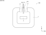
- FIG. 2 is a front view of the current sensor according to the first embodiment.
- FIG. 2 is a side view of the current sensor according to the first embodiment.
- FIG. 11 is a perspective view of a core in a current sensor according to a modified example.
- FIG. 13 is a front view of a current sensor according to another modified example.
- FIG. FIG. 13 is a front view of a current sensor according to another modified example.
- 5B is an enlarged cross-sectional view showing a bus bar and a bus bar through hole in the current sensor of FIG. 5A.
- 5B is a graph showing the effect of misalignment of the bus bars on sensitivity in the current sensor according to the modified example of FIG. 5A .
- FIG. 13 is a front view of a current sensor according to another modified example.
- FIG. 7B is an enlarged cross-sectional view showing a bus bar and a bus bar through hole in the current sensor of FIG. 7A.
- FIG. 13 is a front view of a current sensor according to another modified example.
- 11 is a front view illustrating the temperatures of the core member and the first gap by shading when current is applied to the bus bar.
- FIG. 11 is a front view of a current sensor according to a second embodiment.
- FIG. 11 is a side view of a current sensor according to a second embodiment.
- 4A and 4B are a side view and a graph illustrating the relationship between the position of a magnetic detection unit in a current sensor and magnetic flux density.
- FIG. 11 is a vector diagram showing a simulation result of a magnetic field generated in an energized phase and an adjacent phase by a current flowing through a bus bar of the energized phase.
- FIG. 13 is a front view of a current sensor according to a modified example.
- FIG. 11 is a side view of a current sensor according to a modified example.
- FIG. 11 is a side view of a current sensor according to another modified example.
- FIG. 11 is a side view of a current sensor according to another modified example.
- FIG. 1 is a front view of a conventional current sensor.
- FIG. 1 is a side view of a conventional current sensor.
- Reference coordinates are shown in each drawing as appropriate to show the positional relationship of each component.
- the reference coordinates are defined as the X direction in which the end faces that define the first gap of the core member face each other, the Y direction in which the detection surface of the magnetic detection unit is perpendicular to the X direction, and the Z direction in which the central axis of the ring of the core member faces.
- the current sensor 1 includes a core member 2 and a magnetic detection unit 3 .
- the core member 2 is a member made of a magnetic material, has a first gap 22 sandwiched between end faces 21, and is formed in a ring shape into which the bus bar 4 can be inserted.
- a current to be measured flows through the bus bar 4
- a magnetic field generated from the bus bar 4 is collected in the first gap 22, and the magnetic field in the first gap 22 is detected by the magnetic detector 3.
- the present invention can also be embodied in a mode in which a conductor other than the bus bar 4 is inserted through the core member 2.
- the current sensor 1 measures the current to be measured flowing through the conductor.
- the core member 2 may be configured by stacking a plurality of annular plate materials in the Z direction, the plate thickness direction of which is the Z direction.
- the magnetic detector 3 detects a magnetic field in the first gap 22 that is generated when a current to be measured flows through the bus bar 4.
- the magnetic detector 3 is spaced apart from the bus bar 4 in the Y direction and disposed such that a detection surface 31 is perpendicular to the plate surface of the bus bar 4.
- the bus bar 4 is a conductive material made of copper, brass, aluminum, or the like, through which the current to be measured flows.
- the bus bar 4 is formed in a plate shape, and is disposed so as to penetrate the core member 2, which is formed in an annular shape. Note that, although the bus bar 4 is plate-shaped in this embodiment, it is not limited to being plate-shaped. For example, the cross-sectional shape of the bus bar 4 parallel to the XY plane may be circular.
- FIGS. 16A and 16B are a plan view and a front view of a conventional current sensor 100.
- the current sensor 100 is equipped with a Hall element 103 as a magnetic detector that detects the magnetic field across the first gap 22.
- the detection surface 131 of the Hall element 103 and the end surface 21 of the first gap 22 of the core member 2 are arranged facing each other. Since the area of the end surface 21 of the first gap 22 needs to be approximately the same as the area of the detection surface 131 of the Hall element 103, it has been difficult to make the current sensor 100 smaller and thinner.
- the detection surface 31 of the magnetic detection unit 3 is capable of detecting magnetic field components parallel to the detection surface 31.
- the detection surface 31 is arranged parallel to the direction in which the two end faces 21 that form the first gap 22 face each other, so that the sensitivity direction is the X direction and parallel to the XY plane.
- the magnetic detector 3 is mounted on a substrate 5 made of epoxy glass, ceramic, or the like.
- the surface 51 of the substrate 5, which is parallel to the XY plane, is perpendicular to the end surface 21 of the core member 2, which is parallel to the XZ plane.
- the magnetic detector 3 By mounting the magnetic detector 3 on the substrate 5, i.e. by arranging the magnetic detector 3 so that the detection surface 31 is parallel to the plate surface 51 of the substrate 5, a current sensor that is resistant to vibrations can be obtained. If the magnetic detector 3 is equipped with magnetoresistance effect elements such as GMR elements and TMR elements as detection elements, it can be mounted on the substrate 5.
- the Hall element 103 serving as the magnetic detector is attached to a holding member 105 that is long in the Y direction. For this reason, when vibration is applied to the current sensor 100, the position of the Hall element 103 may change, as shown by the dashed line in the figure. If the position of the Hall element 103 changes, the detection surface 131 will be tilted with respect to the detection magnetic field in the direction opposite the end face 21 (X direction), and the detection accuracy of the current sensor 100 will decrease.
- the magnetic detector 3 is mounted on the substrate 5. Therefore, the inclination of the detection surface 31 with respect to the detection magnetic field can be suppressed without providing a member or structure for holding the magnetic detector 3. Even when vibration is applied to the current sensor 1, the position of the magnetic detector 3 is unlikely to shift in a direction parallel to the plate surface 51 of the substrate 5. Even if the substrate 5 is momentarily deflected in the Z direction, the detection surface 31 will not tilt with respect to the detection magnetic field. In other words, when no vibration is applied to the current sensor 1, the direction of the magnetic field generated in the first gap 22 is the X direction, and the direction in which the magnetic detector 3 can detect the magnetic component at this time is also the X direction.
- the position of the detection surface 31 of the magnetic detector 3 shifts along the side of a cylinder centered on a virtual axis parallel to the X direction, while maintaining the sensitivity axis in the X direction. Therefore, the detection surface 31 is in a state similar to that of being rotated around an imaginary axis parallel to the X direction from the position before the substrate 5 was bent in the Z direction. In other words, the magnetic component that the magnetic detector 3 can detect remains the magnetic component in the X direction. Therefore, it is possible to reduce the deterioration of the detection accuracy of the current sensor 1 due to vibration.
- Figure 2 is a perspective view of the core member 2 in a modified example of the current sensor 1.
- the core member 2 and the substrate 5 are engaged and integrated by inserting the protrusion 23 of the core member 2 into the hole 52 of the substrate 5.
- the method of integrating the core member 2 and the substrate 5 is not limited to this.
- FIG. 3 is a plan view of a current sensor 1a according to another modified example.
- the current sensor 1a shown in the figure differs from the current sensor 1 in that it includes a core member 2a having a second gap 25 different from the first gap 22. Note that the positional relationship of the core member 2a, magnetic detector 3, detection surface 31, bus bar 4, and substrate 5 when viewed in the Y direction is the same as that of the current sensor 1 shown in FIG. 1B.
- the core member 2a By configuring the core member 2a to be divided, it is possible to measure a larger current to be measured using the same magnetic detector 3 and substrate 5 as when measuring a small current to be measured. In the case of a divided core member 2a, it is preferable to integrate the core member 2a and substrate 5 from the viewpoint of stabilizing the positional relationship between the core member 2a and the magnetic detector 3 (see Figure 2).
- the second gap 25 and the first gap 22 are formed on opposite sides of the core member 2a in the Y direction.
- the distance between the opposing end faces 24 that define the second gap 25 is smaller than the distance between the opposing end faces 21 that define the first gap 22.
- the distance between the end faces 24 and the distance between the end faces 21 may each be set according to the magnitude of the current to be measured, but for example, the distance between the end faces 24 may be approximately 0.5 to 3 mm, and the distance between the end faces 21 may be approximately 3 to 10 mm.
- Measurements were performed by passing currents of different magnitudes to be measured through the busbar 4 using the current sensor 1 shown in Fig. 1A and the current sensor 1a shown in Fig. 3.
- the magnetic flux densities detected by the magnetic detection unit 3 are shown in Table 1.
- the distance between the end faces 21 of the first gap 22 in the current sensor 1 and the current sensor 1a was 9 mm, and the distance between the end faces 24 of the second gap 25 in the current sensor 1a was 1 mm.
- Table 1 by using the divided core member 2a, it is possible to adjust the magnetic flux density of the magnetic field detected by the magnetic detector 3. Therefore, it is possible to adjust the measurable range of the current sensor.
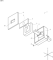
- FIG. 4 is an exploded perspective view of the current sensor 1.
- the current sensor 1 has a housing 6 that contains the core member 2, the magnetic detector 3, and the substrate 5.
- the housing 6 has a bus bar through hole 61 through which the bus bar 4 can be inserted.
- the current sensor 1 uses the magnetic detector 3 to measure the current to be measured that flows through the bus bar 4 when the bus bar 4 is inserted into the bus bar through hole 61 that is provided by penetrating the inside of the ring formed by the core member 2.
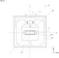
- FIG. 5A is a front view of a current sensor 1b according to another modified example.
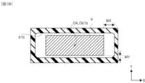
- 5B is an enlarged cross-sectional view of a portion corresponding to line AA in FIG. 4 in an assembled state, showing bus bar 4 and bus bar through hole 61b of current sensor 1b in FIG. 5A.
- the cross section of the busbar through hole 61b in the XY plane is a rectangle that is long in the X direction and in which the two end faces 21 that define the first gap 22 face each other. This makes it possible to suppress the effect of misalignment of the busbar 4 inserted into the busbar through hole 61b on the measurement sensitivity of the current sensor 1b.
- Figure 6 is a graph showing the effect of misalignment of the busbar 4 on the sensitivity of the current sensor 1b according to the modified example of Figure 5A.
- the figure shows the sensitivity variation rate of the current sensor 1b when the busbar 4 is misaligned in the X direction, Y direction, or XY direction from a predetermined position where the center O4 of the busbar 4 and the center O61b of the busbar through hole 61b overlap.
- the cross-sectional shape of the busbar through hole 61b in the housing 6b has a first clearance width MX in the X direction that is larger than a second clearance width MY in the Y direction.
- the first clearance width MX in the X direction in which the end faces 21 that define the first gap 22 face each other is larger than the second clearance width MY in the Y direction that is perpendicular to the direction in which the end faces 21 face each other.
- the busbar through hole 61b With the first margin width MX and the second margin width MY, it becomes easier to insert the busbar 4 into the busbar through hole 61b. Furthermore, even if the position of the busbar 4 in the busbar through hole 61b shifts from a predetermined position, the direction of the shift is the X direction, which has a small effect on the sensitivity of the current sensor 1b. Therefore, even if the busbar 4 shifts from the predetermined position, the current sensor 1b can have a predetermined sensitivity.
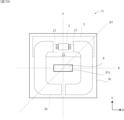
- FIG. 7A is a front view of a current sensor 1c according to another modified example.
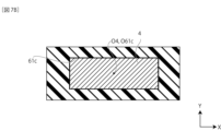
- 7B is an enlarged cross-sectional view of a portion corresponding to line AA in FIG. 4 in an assembled state, showing the bus bar 4 and the bus bar through hole 61c of the current sensor 1c in FIG. 7A.
- the current sensor 1c is different from the current sensor 1b in that the bus bar 4 is held integrally in the housing 6c that holds the core member 2a, the magnetic detector 3, and the substrate 5.
- the bus bar 4 can be held integrally in the housing 6c by forming a part of the bus bar 4 integrally with the housing 6c by insert molding.
- the current sensor 1c and the current sensor 1b have the same configuration in which the bus bar 4 is disposed penetrating the inside of the ring formed by the core member 2a.
- the bus bar 4 is held integrally in the housing 6c, the positional deviation between the center O61c of the bus bar through hole 61c and the center O4 of the bus bar 4 can be reduced, so that the sensitivity fluctuation caused by the positional deviation of the bus bar 4 as shown in FIG. 6 is less likely to occur.
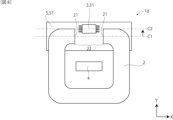
- FIG. 8 is a front view of a current sensor 1d according to another modified example. 1A in that the magnetic detector 3 is disposed at a position offset with respect to the first gap 22 when viewed in the Z direction, which is a direction along the central axis of the ring of the core member 2 and an extension direction of the bus bar 4. That is, the magnetic detector 3 of the current sensor 1d is disposed at a position where the center line C2 in the X direction passing through the center of the width in the Y direction of the magnetic detector 3 is offset with respect to the center line C1 in the X direction passing through the center of the width in the Y direction of the two end faces 21 that form the first gap 22.
- the distance in the Y direction between the center lines C1 and C2 may be set according to the magnitude of the current to be measured, and may be, for example, about 1 to 10 mm.
- the magnetic detector 3 is positioned so that at least a portion of it overlaps with the first gap 22 when viewed in the Z direction, so that the magnetic field formed in the first gap 22 formed by the two end faces 21 can be measured with high accuracy.
- Measurements were performed by passing currents of different magnitudes to be measured through the busbar 4 using the current sensor 1 shown in Fig. 1A and the current sensor 1d shown in Fig. 8.
- the magnetic flux density of the magnetic field detected by the magnetic detection unit 3 in the measurements is shown in the table below.
- the distance between the end faces 21 of the first gap 22 in the current sensor 1 and the current sensor 1d was 9 mm, and the end face 21 was a square with sides of 15 mm.
- the distance in the Y direction between the center line C1 and the center line C2 in the current sensor 1d was 5 mm.
- Second Embodiment 9 is a front view showing the temperature of the core member 2 with shading when the bus bar 4 is energized.
- the bus bar 4 when a current to be measured flows through the bus bar 4, the bus bar 4 generates heat.
- the heat generated at this time is called tilt heat.
- the tilt heat becomes higher as the current to be measured becomes larger. Influenced by the tilt heat from the bus bar 4, the first gap 22 of the core member 2 becomes almost the same temperature as the core member 2, and the space in the first gap 22 also becomes high temperature. Therefore, in the current sensor of this embodiment, the magnetic detection unit 3 is disposed outside the first gap 22 in order to suppress the influence of the tilt heat from the bus bar 4 via the core member 2.
- FIGS. 10A and 10B are a front view and a side view of a current sensor 1e according to the present embodiment.
- the magnetic detector 3 of the current sensor 1e is disposed outside the first gap 22.
- the current sensor 1e is different from the current sensor 1 in that the magnetic detector 3 is disposed at a position shifted in the Z direction from the position of the first gap 22 sandwiched between the end faces 21 when viewed in the Y direction.
- the magnetic detector 3 is planarly mounted on the substrate 5, and the plate surface 51 of the substrate 5 and the end face 21 forming the first gap 22 are orthogonal to each other.
- the magnetic detector 3 is disposed so as to overlap with the first gap 22.
- the configuration of the current sensor 1e is the same as that of the current sensor 1.
- FIG. 11 is a diagram illustrating the relationship between the position of the magnetic detector 3 in the current sensor 1d and the magnetic flux density.
- the current sensor 1e has the magnetic detection unit 3 disposed outside the region of the first gap 22 indicated in gray in Fig. 11, and therefore can suppress the effect of the heat generated by Joule heat generated in the bus bar 4 when current is applied on the magnetic detection unit 3. Therefore, the current sensor 1e has excellent detection accuracy and durability in which detection errors due to temperature drift of the magnetic detection unit 3 are suppressed.
- the magnetic flux density in the area inside the first gap 22 may exceed the upper limit detectable by the magnetic detector 3.
- the magnetic flux density may also exceed the upper limit detectable by the magnetic detector 3 in an area outside the first gap 22 near the side surface 26 of the core member 2. Therefore, in the current sensor 1d, the magnetic detector 3 is disposed in an area where the magnetic flux density is equal to or lower than the upper limit detectable by the magnetic detector 3 when the current to be measured in the busbar 4 to be detected reaches its maximum value.
- the detection surface 31 of the magnetic detector 3 is disposed at a position away from the side surface 26 of the core member 2 by a distance equal to or higher than the distance at which the magnetic flux density is equal to or lower than the upper limit detectable. This arrangement results in the current sensor 1e being capable of handling large currents.
- the distance Dz from the side surface of the core member 2 to the detection surface 31 is preferably 1.0D to 1.5D, more preferably 1.0D to 1.3D, and even more preferably 1.0D to 1.2D.
- This configuration makes it possible to provide a current sensor 1e that has excellent detection accuracy and can handle large currents.
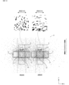
- Figure 12 is a vector diagram showing the simulation results of the magnetic field generated in the current-carrying phase and the adjacent phase when current is passed only through the bus bar 4 of the current-carrying phase, without passing current through the bus bar 4 of the adjacent phase, and shows a current sensor 1f equipped with multiple measurement phases.
- the current sensor 1f has a plurality of measurement phases each having a core member 2 and a magnetic detector 3, it is preferable to suppress the influence on adjacent phases in order to improve the detection accuracy of the magnetic field.
- the magnetic detector 3 is disposed in the Z direction on the upper side of the paper surface of FIG. 12 outside the first gap 22. That is, when viewed in a direction (Y direction) perpendicular to the direction (X direction) in which the two end faces 21 forming the first gap 22 face each other, the detection surface 31 of the magnetic detector 3 is disposed so as to be shifted from the first gap 22 in a direction along the central axis of the ring of the core member (Z direction). Also, when viewed in the Z direction, the detection surface 31 of the magnetic detector 3 is disposed so as to overlap the first gap 22 (see FIG. 10A).
- the direction of the magnetic field generated from the adjacent energized phase is the Z direction.
- the sensitivity direction of the magnetic detector 3 of the adjacent phase that detects the magnetic field in the X direction generated near the first gap 22 is the X direction.
- the magnetic detector 3 disposed in the adjacent phase is less susceptible to the influence of the adjacent energized phase because the magnetic field from the adjacent energized phase is perpendicular to the sensitivity direction.
- the direction of the magnetic field generated from the adjacent adjacent phase becomes the Z direction in the region where the magnetic detector 3 is arranged in the current-carrying phase. Therefore, by disposing the magnetic detector 3 at a position shifted in the Z direction from the first gap 22, the influence of the magnetic field from adjacent phases is suppressed, resulting in a multi-phase type current sensor 1f with good magnetic field detection accuracy.
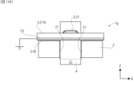
- 13A and 13B are a front view and a side view of a current sensor 1g according to a modified example. 10A and 10B in that a grounded substrate 5 is disposed between the core member 2 and the magnetic detector 3. That is, the magnetic detector 3 is planar-mounted on one surface 51A of the substrate 5, and the other surface 51B of the substrate 5 faces the side surface 26 of the core member 2. With this configuration, electromagnetic noise picked up by the core member 2 can be shielded by the solid GND surface 53 of the substrate 5, resulting in a current sensor 1g with excellent noise resistance.
- FIG. 14 is a front view of a current sensor 1h according to another modified example.
- a sub-magnetic detector unit 3S is disposed on a surface 51B opposite to a surface 51A on which the magnetic detector unit 3 is disposed on the substrate 5.
- a magnetoresistance effect element can be used as the detection element of the sub-magnetic detection unit 3S of the current sensor 1h.
- the sub-magnetic detection unit 3S is disposed outside the first gap 22 of the core member 2, thereby reducing the effect of the heat generated by the busbar 4.
- FIG. 15 is a front view of a current sensor 1i according to another modified example.
- a Hall sensor can be used as the detection element of the sub-magnetic detection unit 3S.
- the detection element of the sub-magnetic detection unit 3S is disposed within the first gap 22 of the core member 2.
- a Hall sensor When a Hall sensor is arranged as a sub-magnetic detection unit 3S on the surface 51B opposite to the surface 51A on which the magnetic detection unit 3 of the substrate 5 is mounted, functional safety can be achieved by redundancy, and the detection element method is different. Since the magnetic detection unit 3 and the sub-magnetic detection unit 3S have different failure modes, it is unlikely that the magnetic detection unit 3 and the sub-magnetic detection unit 3S will fail simultaneously, resulting in a current sensor 1i with excellent reliability and safety.
- the present invention is useful as a current sensor that is attached to various devices to measure the current to be measured in order to control or monitor the devices.
Landscapes
- Physics & Mathematics (AREA)
- General Physics & Mathematics (AREA)
- Measuring Instrument Details And Bridges, And Automatic Balancing Devices (AREA)
Priority Applications (3)
| Application Number | Priority Date | Filing Date | Title |
|---|---|---|---|
| EP23901769.2A EP4636409A1 (en) | 2022-12-12 | 2023-10-02 | Current sensor |
| JP2024564177A JPWO2024127770A1 (https=) | 2022-12-12 | 2023-10-02 | |
| US19/198,222 US20250271470A1 (en) | 2022-12-12 | 2025-05-05 | Current Sensor |
Applications Claiming Priority (2)
| Application Number | Priority Date | Filing Date | Title |
|---|---|---|---|
| JP2022-197903 | 2022-12-12 | ||
| JP2022197903 | 2022-12-12 |
Related Child Applications (1)
| Application Number | Title | Priority Date | Filing Date |
|---|---|---|---|
| US19/198,222 Continuation US20250271470A1 (en) | 2022-12-12 | 2025-05-05 | Current Sensor |
Publications (1)
| Publication Number | Publication Date |
|---|---|
| WO2024127770A1 true WO2024127770A1 (ja) | 2024-06-20 |
Family
ID=91484786
Family Applications (1)
| Application Number | Title | Priority Date | Filing Date |
|---|---|---|---|
| PCT/JP2023/035826 Ceased WO2024127770A1 (ja) | 2022-12-12 | 2023-10-02 | 電流センサ |
Country Status (4)
| Country | Link |
|---|---|
| US (1) | US20250271470A1 (https=) |
| EP (1) | EP4636409A1 (https=) |
| JP (1) | JPWO2024127770A1 (https=) |
| WO (1) | WO2024127770A1 (https=) |
Cited By (1)
| Publication number | Priority date | Publication date | Assignee | Title |
|---|---|---|---|---|
| WO2025074794A1 (ja) * | 2023-10-03 | 2025-04-10 | アルプスアルパイン株式会社 | 電流センサおよび電流センサの製造方法 |
Citations (8)
| Publication number | Priority date | Publication date | Assignee | Title |
|---|---|---|---|---|
| JP2008224260A (ja) * | 2007-03-09 | 2008-09-25 | Tamura Seisakusho Co Ltd | 電流検出器 |
| JP2012247197A (ja) | 2011-05-25 | 2012-12-13 | Sumitomo Wiring Syst Ltd | 電流検出装置及び磁性体コア |
| JP2013142579A (ja) | 2012-01-10 | 2013-07-22 | Auto Network Gijutsu Kenkyusho:Kk | 電流検出装置 |
| WO2015190155A1 (ja) * | 2014-06-10 | 2015-12-17 | アルプス・グリーンデバイス株式会社 | 電流センサ |
| WO2016080135A1 (ja) * | 2014-11-19 | 2016-05-26 | 株式会社東海理化電機製作所 | 電流センサ |
| JP2019115083A (ja) * | 2017-12-20 | 2019-07-11 | トヨタ自動車株式会社 | 電力制御ユニット |
| JP2020134497A (ja) * | 2019-02-13 | 2020-08-31 | 甲神電機株式会社 | 電流センサ |
| JP2022170628A (ja) * | 2021-04-28 | 2022-11-10 | 甲神電機株式会社 | 電流検出装置 |
-
2023
- 2023-10-02 JP JP2024564177A patent/JPWO2024127770A1/ja active Pending
- 2023-10-02 EP EP23901769.2A patent/EP4636409A1/en active Pending
- 2023-10-02 WO PCT/JP2023/035826 patent/WO2024127770A1/ja not_active Ceased
-
2025
- 2025-05-05 US US19/198,222 patent/US20250271470A1/en active Pending
Patent Citations (8)
| Publication number | Priority date | Publication date | Assignee | Title |
|---|---|---|---|---|
| JP2008224260A (ja) * | 2007-03-09 | 2008-09-25 | Tamura Seisakusho Co Ltd | 電流検出器 |
| JP2012247197A (ja) | 2011-05-25 | 2012-12-13 | Sumitomo Wiring Syst Ltd | 電流検出装置及び磁性体コア |
| JP2013142579A (ja) | 2012-01-10 | 2013-07-22 | Auto Network Gijutsu Kenkyusho:Kk | 電流検出装置 |
| WO2015190155A1 (ja) * | 2014-06-10 | 2015-12-17 | アルプス・グリーンデバイス株式会社 | 電流センサ |
| WO2016080135A1 (ja) * | 2014-11-19 | 2016-05-26 | 株式会社東海理化電機製作所 | 電流センサ |
| JP2019115083A (ja) * | 2017-12-20 | 2019-07-11 | トヨタ自動車株式会社 | 電力制御ユニット |
| JP2020134497A (ja) * | 2019-02-13 | 2020-08-31 | 甲神電機株式会社 | 電流センサ |
| JP2022170628A (ja) * | 2021-04-28 | 2022-11-10 | 甲神電機株式会社 | 電流検出装置 |
Non-Patent Citations (1)
| Title |
|---|
| See also references of EP4636409A1 |
Cited By (1)
| Publication number | Priority date | Publication date | Assignee | Title |
|---|---|---|---|---|
| WO2025074794A1 (ja) * | 2023-10-03 | 2025-04-10 | アルプスアルパイン株式会社 | 電流センサおよび電流センサの製造方法 |
Also Published As
| Publication number | Publication date |
|---|---|
| US20250271470A1 (en) | 2025-08-28 |
| EP4636409A1 (en) | 2025-10-22 |
| JPWO2024127770A1 (https=) | 2024-06-20 |
Similar Documents
| Publication | Publication Date | Title |
|---|---|---|
| US9557352B2 (en) | Current detection structure | |
| CN107533089B (zh) | 电流传感器 | |
| US11313884B2 (en) | Current sensor | |
| US20120187943A1 (en) | Current difference sensors, systems and methods | |
| US10274523B2 (en) | Current sensor including a first current sensor and a second current sensor unit | |
| US20140232376A1 (en) | Current sensor | |
| JP2015137892A (ja) | 電流検出構造 | |
| JP2013044705A (ja) | 電流検出装置 | |
| WO2021070834A1 (ja) | 電流検出装置 | |
| JP2008039734A (ja) | 電流センサ | |
| US20130076341A1 (en) | High current sensors | |
| CN116359582A (zh) | 具有定位稳定性的电流感测 | |
| JPWO2018163685A1 (ja) | 電流センサ | |
| JP2022189812A (ja) | V字型に配置された磁界センサを備える電流センサ | |
| JP6540802B2 (ja) | 電流センサ | |
| WO2024127770A1 (ja) | 電流センサ | |
| JP7489498B2 (ja) | 電流検出装置 | |
| JP4066716B2 (ja) | 位置検出センサ | |
| JP7514958B2 (ja) | 電流センサ及び電気装置 | |
| JP2014055791A (ja) | 電流センサ | |
| JP7003608B2 (ja) | 電流センサ | |
| JP4506641B2 (ja) | 電流センサ装置 | |
| JP3191252U (ja) | 電流センサ | |
| JP4873348B2 (ja) | 電流センサおよび電流検出装置 | |
| WO2021070833A1 (ja) | 磁気センサ及びこれを備えた電流検出装置 |
Legal Events
| Date | Code | Title | Description |
|---|---|---|---|
| 121 | Ep: the epo has been informed by wipo that ep was designated in this application |
Ref document number: 23901769 Country of ref document: EP Kind code of ref document: A1 |
|
| WWE | Wipo information: entry into national phase |
Ref document number: 2024564177 Country of ref document: JP |
|
| WWE | Wipo information: entry into national phase |
Ref document number: 2023901769 Country of ref document: EP |
|
| NENP | Non-entry into the national phase |
Ref country code: DE |
|
| ENP | Entry into the national phase |
Ref document number: 2023901769 Country of ref document: EP Effective date: 20250714 |
|
| WWP | Wipo information: published in national office |
Ref document number: 2023901769 Country of ref document: EP |