WO2024127199A1 - 電子機器 - Google Patents
電子機器 Download PDFInfo
- Publication number
- WO2024127199A1 WO2024127199A1 PCT/IB2023/062447 IB2023062447W WO2024127199A1 WO 2024127199 A1 WO2024127199 A1 WO 2024127199A1 IB 2023062447 W IB2023062447 W IB 2023062447W WO 2024127199 A1 WO2024127199 A1 WO 2024127199A1
- Authority
- WO
- WIPO (PCT)
- Prior art keywords
- display
- circuit
- transistor
- insulator
- layer
- Prior art date
- Legal status (The legal status is an assumption and is not a legal conclusion. Google has not performed a legal analysis and makes no representation as to the accuracy of the status listed.)
- Ceased
Links
Images























Classifications
-
- G—PHYSICS
- G09—EDUCATION; CRYPTOGRAPHY; DISPLAY; ADVERTISING; SEALS
- G09G—ARRANGEMENTS OR CIRCUITS FOR CONTROL OF INDICATING DEVICES USING STATIC MEANS TO PRESENT VARIABLE INFORMATION
- G09G3/00—Control arrangements or circuits, of interest only in connection with visual indicators other than cathode-ray tubes
- G09G3/20—Control arrangements or circuits, of interest only in connection with visual indicators other than cathode-ray tubes for presentation of an assembly of a number of characters, e.g. a page, by composing the assembly by combination of individual elements arranged in a matrix no fixed position being assigned to or needed to be assigned to the individual characters or partial characters
- G09G3/22—Control arrangements or circuits, of interest only in connection with visual indicators other than cathode-ray tubes for presentation of an assembly of a number of characters, e.g. a page, by composing the assembly by combination of individual elements arranged in a matrix no fixed position being assigned to or needed to be assigned to the individual characters or partial characters using controlled light sources
- G09G3/30—Control arrangements or circuits, of interest only in connection with visual indicators other than cathode-ray tubes for presentation of an assembly of a number of characters, e.g. a page, by composing the assembly by combination of individual elements arranged in a matrix no fixed position being assigned to or needed to be assigned to the individual characters or partial characters using controlled light sources using electroluminescent panels
- G09G3/32—Control arrangements or circuits, of interest only in connection with visual indicators other than cathode-ray tubes for presentation of an assembly of a number of characters, e.g. a page, by composing the assembly by combination of individual elements arranged in a matrix no fixed position being assigned to or needed to be assigned to the individual characters or partial characters using controlled light sources using electroluminescent panels semiconductive, e.g. using light-emitting diodes [LED]
- G09G3/3208—Control arrangements or circuits, of interest only in connection with visual indicators other than cathode-ray tubes for presentation of an assembly of a number of characters, e.g. a page, by composing the assembly by combination of individual elements arranged in a matrix no fixed position being assigned to or needed to be assigned to the individual characters or partial characters using controlled light sources using electroluminescent panels semiconductive, e.g. using light-emitting diodes [LED] organic, e.g. using organic light-emitting diodes [OLED]
- G09G3/3225—Control arrangements or circuits, of interest only in connection with visual indicators other than cathode-ray tubes for presentation of an assembly of a number of characters, e.g. a page, by composing the assembly by combination of individual elements arranged in a matrix no fixed position being assigned to or needed to be assigned to the individual characters or partial characters using controlled light sources using electroluminescent panels semiconductive, e.g. using light-emitting diodes [LED] organic, e.g. using organic light-emitting diodes [OLED] using an active matrix
- G09G3/3233—Control arrangements or circuits, of interest only in connection with visual indicators other than cathode-ray tubes for presentation of an assembly of a number of characters, e.g. a page, by composing the assembly by combination of individual elements arranged in a matrix no fixed position being assigned to or needed to be assigned to the individual characters or partial characters using controlled light sources using electroluminescent panels semiconductive, e.g. using light-emitting diodes [LED] organic, e.g. using organic light-emitting diodes [OLED] using an active matrix with pixel circuitry controlling the current through the light-emitting element
-
- G—PHYSICS
- G04—HOROLOGY
- G04G—ELECTRONIC TIME-PIECES
- G04G9/00—Visual time or date indication means
-
- G—PHYSICS
- G09—EDUCATION; CRYPTOGRAPHY; DISPLAY; ADVERTISING; SEALS
- G09G—ARRANGEMENTS OR CIRCUITS FOR CONTROL OF INDICATING DEVICES USING STATIC MEANS TO PRESENT VARIABLE INFORMATION
- G09G3/00—Control arrangements or circuits, of interest only in connection with visual indicators other than cathode-ray tubes
- G09G3/20—Control arrangements or circuits, of interest only in connection with visual indicators other than cathode-ray tubes for presentation of an assembly of a number of characters, e.g. a page, by composing the assembly by combination of individual elements arranged in a matrix no fixed position being assigned to or needed to be assigned to the individual characters or partial characters
-
- G—PHYSICS
- G09—EDUCATION; CRYPTOGRAPHY; DISPLAY; ADVERTISING; SEALS
- G09G—ARRANGEMENTS OR CIRCUITS FOR CONTROL OF INDICATING DEVICES USING STATIC MEANS TO PRESENT VARIABLE INFORMATION
- G09G3/00—Control arrangements or circuits, of interest only in connection with visual indicators other than cathode-ray tubes
- G09G3/20—Control arrangements or circuits, of interest only in connection with visual indicators other than cathode-ray tubes for presentation of an assembly of a number of characters, e.g. a page, by composing the assembly by combination of individual elements arranged in a matrix no fixed position being assigned to or needed to be assigned to the individual characters or partial characters
- G09G3/22—Control arrangements or circuits, of interest only in connection with visual indicators other than cathode-ray tubes for presentation of an assembly of a number of characters, e.g. a page, by composing the assembly by combination of individual elements arranged in a matrix no fixed position being assigned to or needed to be assigned to the individual characters or partial characters using controlled light sources
- G09G3/30—Control arrangements or circuits, of interest only in connection with visual indicators other than cathode-ray tubes for presentation of an assembly of a number of characters, e.g. a page, by composing the assembly by combination of individual elements arranged in a matrix no fixed position being assigned to or needed to be assigned to the individual characters or partial characters using controlled light sources using electroluminescent panels
- G09G3/32—Control arrangements or circuits, of interest only in connection with visual indicators other than cathode-ray tubes for presentation of an assembly of a number of characters, e.g. a page, by composing the assembly by combination of individual elements arranged in a matrix no fixed position being assigned to or needed to be assigned to the individual characters or partial characters using controlled light sources using electroluminescent panels semiconductive, e.g. using light-emitting diodes [LED]
- G09G3/3208—Control arrangements or circuits, of interest only in connection with visual indicators other than cathode-ray tubes for presentation of an assembly of a number of characters, e.g. a page, by composing the assembly by combination of individual elements arranged in a matrix no fixed position being assigned to or needed to be assigned to the individual characters or partial characters using controlled light sources using electroluminescent panels semiconductive, e.g. using light-emitting diodes [LED] organic, e.g. using organic light-emitting diodes [OLED]
- G09G3/3225—Control arrangements or circuits, of interest only in connection with visual indicators other than cathode-ray tubes for presentation of an assembly of a number of characters, e.g. a page, by composing the assembly by combination of individual elements arranged in a matrix no fixed position being assigned to or needed to be assigned to the individual characters or partial characters using controlled light sources using electroluminescent panels semiconductive, e.g. using light-emitting diodes [LED] organic, e.g. using organic light-emitting diodes [OLED] using an active matrix
-
- H—ELECTRICITY
- H10—SEMICONDUCTOR DEVICES; ELECTRIC SOLID-STATE DEVICES NOT OTHERWISE PROVIDED FOR
- H10B—ELECTRONIC MEMORY DEVICES
- H10B12/00—Dynamic random access memory [DRAM] devices
-
- H—ELECTRICITY
- H10—SEMICONDUCTOR DEVICES; ELECTRIC SOLID-STATE DEVICES NOT OTHERWISE PROVIDED FOR
- H10B—ELECTRONIC MEMORY DEVICES
- H10B41/00—Electrically erasable-and-programmable ROM [EEPROM] devices comprising floating gates
- H10B41/70—Electrically erasable-and-programmable ROM [EEPROM] devices comprising floating gates the floating gate being an electrode shared by two or more components
-
- H—ELECTRICITY
- H10—SEMICONDUCTOR DEVICES; ELECTRIC SOLID-STATE DEVICES NOT OTHERWISE PROVIDED FOR
- H10D—INORGANIC ELECTRIC SEMICONDUCTOR DEVICES
- H10D30/00—Field-effect transistors [FET]
- H10D30/60—Insulated-gate field-effect transistors [IGFET]
- H10D30/67—Thin-film transistors [TFT]
-
- H—ELECTRICITY
- H10—SEMICONDUCTOR DEVICES; ELECTRIC SOLID-STATE DEVICES NOT OTHERWISE PROVIDED FOR
- H10D—INORGANIC ELECTRIC SEMICONDUCTOR DEVICES
- H10D84/00—Integrated devices formed in or on semiconductor substrates that comprise only semiconducting layers, e.g. on Si wafers or on GaAs-on-Si wafers
-
- H—ELECTRICITY
- H10—SEMICONDUCTOR DEVICES; ELECTRIC SOLID-STATE DEVICES NOT OTHERWISE PROVIDED FOR
- H10D—INORGANIC ELECTRIC SEMICONDUCTOR DEVICES
- H10D84/00—Integrated devices formed in or on semiconductor substrates that comprise only semiconducting layers, e.g. on Si wafers or on GaAs-on-Si wafers
- H10D84/01—Manufacture or treatment
- H10D84/0123—Integrating together multiple components covered by H10D12/00 or H10D30/00, e.g. integrating multiple IGBTs
- H10D84/0126—Integrating together multiple components covered by H10D12/00 or H10D30/00, e.g. integrating multiple IGBTs the components including insulated gates, e.g. IGFETs
-
- H—ELECTRICITY
- H10—SEMICONDUCTOR DEVICES; ELECTRIC SOLID-STATE DEVICES NOT OTHERWISE PROVIDED FOR
- H10D—INORGANIC ELECTRIC SEMICONDUCTOR DEVICES
- H10D84/00—Integrated devices formed in or on semiconductor substrates that comprise only semiconducting layers, e.g. on Si wafers or on GaAs-on-Si wafers
- H10D84/01—Manufacture or treatment
- H10D84/02—Manufacture or treatment characterised by using material-based technologies
- H10D84/03—Manufacture or treatment characterised by using material-based technologies using Group IV technology, e.g. silicon technology or silicon-carbide [SiC] technology
- H10D84/038—Manufacture or treatment characterised by using material-based technologies using Group IV technology, e.g. silicon technology or silicon-carbide [SiC] technology using silicon technology, e.g. SiGe
-
- G—PHYSICS
- G09—EDUCATION; CRYPTOGRAPHY; DISPLAY; ADVERTISING; SEALS
- G09G—ARRANGEMENTS OR CIRCUITS FOR CONTROL OF INDICATING DEVICES USING STATIC MEANS TO PRESENT VARIABLE INFORMATION
- G09G2300/00—Aspects of the constitution of display devices
- G09G2300/08—Active matrix structure, i.e. with use of active elements, inclusive of non-linear two terminal elements, in the pixels together with light emitting or modulating elements
- G09G2300/0809—Several active elements per pixel in active matrix panels
- G09G2300/0814—Several active elements per pixel in active matrix panels used for selection purposes, e.g. logical AND for partial update
-
- G—PHYSICS
- G09—EDUCATION; CRYPTOGRAPHY; DISPLAY; ADVERTISING; SEALS
- G09G—ARRANGEMENTS OR CIRCUITS FOR CONTROL OF INDICATING DEVICES USING STATIC MEANS TO PRESENT VARIABLE INFORMATION
- G09G2300/00—Aspects of the constitution of display devices
- G09G2300/08—Active matrix structure, i.e. with use of active elements, inclusive of non-linear two terminal elements, in the pixels together with light emitting or modulating elements
- G09G2300/0809—Several active elements per pixel in active matrix panels
- G09G2300/0842—Several active elements per pixel in active matrix panels forming a memory circuit, e.g. a dynamic memory with one capacitor
- G09G2300/0857—Static memory circuit, e.g. flip-flop
-
- G—PHYSICS
- G09—EDUCATION; CRYPTOGRAPHY; DISPLAY; ADVERTISING; SEALS
- G09G—ARRANGEMENTS OR CIRCUITS FOR CONTROL OF INDICATING DEVICES USING STATIC MEANS TO PRESENT VARIABLE INFORMATION
- G09G2330/00—Aspects of power supply; Aspects of display protection and defect management
- G09G2330/02—Details of power systems and of start or stop of display operation
- G09G2330/021—Power management, e.g. power saving
-
- G—PHYSICS
- G09—EDUCATION; CRYPTOGRAPHY; DISPLAY; ADVERTISING; SEALS
- G09G—ARRANGEMENTS OR CIRCUITS FOR CONTROL OF INDICATING DEVICES USING STATIC MEANS TO PRESENT VARIABLE INFORMATION
- G09G2330/00—Aspects of power supply; Aspects of display protection and defect management
- G09G2330/04—Display protection
- G09G2330/045—Protection against panel overheating
Definitions
- This specification describes electronic devices, display systems having the electronic devices, and semiconductor devices that the electronic devices have.
- one embodiment of the present invention is not limited to the above technical field.
- Examples of technical fields of one embodiment of the present invention disclosed in this specification and the like include semiconductor devices, display devices, light-emitting devices, power storage devices, memory devices, electronic devices, lighting devices, input devices, input/output devices, driving methods thereof, and manufacturing methods thereof.
- wrist-worn electronic devices may have a display, as well as various sensors, a CPU for controlling the various sensors, and memory for storing data (see, for example, Patent Document 1).
- SoC System on Chip
- GPU Graphics Processing Unit
- Semiconductor devices that have become more powerful through SoC technology have achieved both miniaturization and high performance through the use of transistors in stacked element layers.
- the increased performance of semiconductor devices is in a trade-off relationship with the demand for increased power consumption or miniaturization of the semiconductor device. In other words, it has been difficult to achieve both high performance and reduced power consumption or miniaturization of semiconductor devices.
- One aspect of the present invention has an object to provide a novel electronic device, etc.
- one aspect of the present invention has an object to provide an electronic device, etc. with a novel structure that can reduce the size of a semiconductor device in an electronic device having a semiconductor device with improved performance due to SoC.
- one aspect of the present invention has an object to provide an electronic device, etc. with a novel structure that can suppress increases in heat generation and power consumption in an electronic device having a semiconductor device with improved performance due to SoC.
- one aspect of the present invention has an object to provide an electronic device, etc. with a novel structure that can achieve both improved performance of the semiconductor device and suppression of power consumption or heat generation of the semiconductor device.
- one aspect of the present invention has an object to provide an electronic device, etc. with a novel structure that is highly convenient.
- One aspect of the present invention is an electronic device having a semiconductor device, the semiconductor device having a logic circuit section provided in a plurality of element layers, a display control section, and a display section, the display section having a plurality of display regions, the display control section having a plurality of driver circuit sections, the plurality of display regions having pixel circuits that control the light emission of a light-emitting device, the plurality of driver circuit sections having driver circuits that control the pixel circuits, each of the plurality of display regions being provided at a position overlapping with a region in which any one of the plurality of driver circuit sections is provided, the logic circuit section having a calculation device, and the calculation device having a function of controlling the operating state or the stopped state of the driver circuit corresponding to the pixel circuit of the display region depending on whether image data in each of the plurality of display regions has been updated.
- an electronic device preferably has a first element layer, a second element layer, and a third element layer, the first element layer having a first transistor having a semiconductor layer having silicon in a channel formation region, the second element layer having a second transistor having a semiconductor layer having a metal oxide in a channel formation region, and the third element layer having a light-emitting device.
- the electronic device preferably has a calculation device having a scan flip-flop and a backup circuit electrically connected to the scan flip-flop, the first element layer is provided with the scan flip-flop and a drive circuit section, and the second element layer is provided with the backup circuit and pixel circuit.
- the backup circuit is preferably an electronic device that has a function of retaining data held in the scan flip-flops while the computing device is not operating, even when the supply of power supply voltage is stopped.
- the metal oxide preferably includes In, Ga, and Zn.
- the image data is image data for displaying a second hand, an hour hand, and a minute hand
- the computing device is an electronic device that operates a drive circuit corresponding to a pixel circuit of a display area that displays the second hand, an hour hand, and a minute hand, and stops a drive circuit corresponding to a pixel circuit of a display area that does not display the second hand, an hour hand, and a minute hand.
- One aspect of the present invention can provide a novel electronic device, etc.
- one aspect of the present invention can provide an electronic device, etc. with a novel configuration that can reduce the size of a semiconductor device in an electronic device having a semiconductor device whose performance has been improved by adopting SoC.
- one aspect of the present invention can provide an electronic device, etc. with a novel configuration that can suppress increases in heat generation and power consumption in an electronic device having a semiconductor device whose performance has been improved by adopting SoC.
- one aspect of the present invention can provide an electronic device, etc. with a novel configuration that can achieve both high performance of the semiconductor device and suppression of power consumption or heat generation of the semiconductor device.
- one aspect of the present invention can provide an electronic device, etc. with a novel configuration that is highly convenient.
- FIGS. 1A and 1B are diagrams illustrating configuration examples of a semiconductor device and an electronic device.
- 2A and 2B are diagrams illustrating a configuration example of a semiconductor device.
- 3A to 3C are diagrams for explaining a configuration example of a semiconductor device.
- 4A and 4B are diagrams illustrating an example of the configuration of an electronic device.
- FIG. 5 is a flowchart illustrating an example of the configuration of an electronic device.
- 6A to 6F are diagrams for explaining configuration examples of a semiconductor device.
- FIG. 7 is a diagram illustrating a configuration example of a semiconductor device.
- FIG. 8 is a diagram illustrating a configuration example of a semiconductor device.
- 9A to 9C are diagrams illustrating an example of the configuration of a semiconductor device.
- 10A and 10B are diagrams illustrating a configuration example of a semiconductor device.
- 11A and 11B are diagrams illustrating a configuration example of a semiconductor device.
- 12A and 12B are circuit diagrams showing configuration examples of pixel circuits.
- 13A to 13D are circuit diagrams showing configuration examples of pixel circuits.
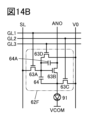
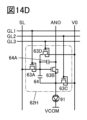
- 14A to 14D are circuit diagrams showing configuration examples of pixel circuits.
- FIG. 15 is a block diagram illustrating an example of the configuration of the arithmetic unit.
- 16A and 16B are circuit diagrams illustrating an example of the configuration of the arithmetic unit.
- FIG. 17 is a timing chart showing an example of the configuration of the arithmetic unit.
- 18A and 18B are a block diagram and a circuit diagram showing a configuration example of a memory circuit.
- FIG. 19A to 19F are circuit diagrams showing configuration examples of memory circuits.
- Fig. 20A is a schematic plan view showing a configuration example of a semiconductor device
- Fig. 20B and Fig. 20C are schematic cross-sectional views showing the configuration example of a semiconductor device.
- 21A and 21B are schematic cross-sectional views showing a configuration example of a semiconductor device.
- FIG. 22 is a schematic cross-sectional view showing a configuration example of a semiconductor device.
- 23A to 23C are schematic cross-sectional views showing configuration examples of a semiconductor device.
- 24A to 24G are diagrams illustrating configuration examples of electronic devices.
- 25A to 25H are diagrams for explaining configuration examples of a semiconductor device.
- ordinal numbers "first,” “second,” and “third” are used to avoid confusion between components. Therefore, they do not limit the number of components. Furthermore, they do not limit the order of the components. For example, a component referred to as “first” in one embodiment of this specification may be a component referred to as “second” in another embodiment or in the claims. For example, a component referred to as “first” in one embodiment of this specification may be omitted in another embodiment or in the claims.
- the power supply potential VDD may be abbreviated to potential VDD, VDD, etc. This also applies to other components (for example, signals, voltages, circuits, elements, electrodes, wiring, etc.).
- identification symbols such as "_1”, “_2”, “[n]”, “[m, n]”, etc. may be added to the reference symbol.
- the second wiring GL is described as wiring GL_2.
- Examples of electronic device configurations> 1A is a block diagram illustrating a semiconductor device included in an electronic device of one embodiment of the present invention.
- the semiconductor device 100 illustrated in FIG. 1A includes, as an example, a logic circuit portion 31, a display control portion 50, and a display portion 60.
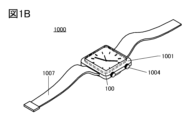
- FIG. 1B is an example of a perspective view of electronic device 1000 having semiconductor device 100 shown in FIG. 1A.
- Electronic device 1000 shown in FIG. 1B is a wristwatch-type electronic device that has a function of displaying an analog clock with hour, minute, and second hands.
- Electronic device 1000 has a configuration in which semiconductor device 100 shown in FIG. 1A is housed in housing 1001 to which operation unit 1004 and band 1007 are attached.
- Electronic device 1000 shown in FIG. 1B has a function as a so-called smart watch.
- the logic circuit unit 31 has a function of controlling the display control unit 50 according to image data. Specifically, the logic circuit unit 31 has a function of controlling the pause operation or resume operation of the drive circuit unit 51 of the divided display control unit 50 according to image data.
- the drive circuit of the drive circuit unit 51 performs an operation of not outputting image data in addition to holding the scanning signal at a low level, and puts the drive circuit unit 51 in a stopped state.
- the supply of control signals such as a clock signal to the drive circuit may be stopped at the same time. This operation allows the pixel circuit of the display unit 60 to hold the image data supplied in the previous period.
- the display control unit 50 has a drive circuit for controlling the pixel circuits of the display unit 60.
- the display control unit 50 has a drive circuit unit 51 (drive circuit units 51_1 to 51_n) (n is an integer of 2 or more).
- Each drive circuit unit 51 has a configuration in which a drive circuit is provided for each of a plurality of regions (sections).
- the drive circuit of the drive circuit unit 51 is electrically connected to the pixel circuits of the display unit 60.
- the drive circuit has a function of supplying image data and scanning signals to the display unit 60.
- the drive circuit that supplies the scanning signals to the display unit 60 may be called a gate driver circuit or a scanning line drive circuit.
- the drive circuit that supplies image data to the display unit 60 may be called a source driver circuit or a signal line drive circuit.
- the drive circuit may be a variety of circuits such as a shift register, a level shifter, an inverter, a latch, an analog switch, or a logic circuit.
- the display unit 60 has a plurality of pixel circuits for displaying an image based on image data.
- the pixel circuits are circuits that control display devices such as light-emitting devices.
- the display unit 60 has a plurality of display areas 61 (display areas 61_1 to 61_n).
- the display areas 61 are sometimes called sub-display units.
- Each of the display areas 61 has a configuration in which a pixel circuit is provided for each of a plurality of areas (sections).
- FIG. 2A is a diagram showing the display unit 60 when the semiconductor device 100 is housed in the housing 1001 of the electronic device 1000.
- the display control unit 50 (not shown) is disposed in a position overlapping the display unit 60.
- the display unit 60 has display areas 61_1 to 61_13.
- the number of divided areas is shown as 13.
- the number of divisions of the display area on the display unit 60 may be other than 13. For example, it may be a 12-division display area according to the number of dials displayed on the analog clock. Or, the area of the analog clock dial may be divided into 6 equal parts, and a central display area may be added to make a 7-division display area. Or, the area of the analog clock dial may be divided into 4 equal parts, and a central display area may be added to make a 5-division display area. Or, the area of the analog clock dial may be divided into 2 equal parts, and a central display area may be added to make a 3-division display area.
- FIG. 2B is a schematic perspective view illustrating the element layer 30 and element layer 40 in which the display control unit 50 and the display unit 60 are provided.
- the element layer 40 is provided by stacking it with the element layer 30.
- the display control unit 50 provided in the element layer 30 is provided in a position overlapping with the display unit 60 provided in the element layer 40.
- the display control unit 50 in the element layer 30 is composed of Si CMOS, i.e., transistors (Si transistors) that have silicon in the channel formation region.
- the element layer 30 is a layer that has Si transistors.
- silicon with high crystallinity such as single crystal silicon or polycrystalline silicon, because this allows for high field effect mobility and faster operation.
- the display portion 60 of the element layer 40 is composed of an OS transistor, that is, a transistor having an oxide semiconductor in its channel formation region.
- the element layer 40 is a layer having an OS transistor.
- OS transistors have the characteristic of having a very low off-state current. Therefore, when OS transistors are used as transistors in the display unit 60 in which pixel circuits are provided, image data written to the pixel circuits can be retained for a long period of time. This reduces the frequency with which image data is rewritten, leading to lower power consumption.
- the display unit 60 has a plurality of display areas 61 (61_1 to 61_13).
- the display control unit 50 also has a drive circuit unit 51 (51_1 to 51_13).
- the drive circuit unit 51 has a drive circuit that can drive the plurality of display areas 61 separately.
- FIG. 3A is a schematic diagram for explaining the configuration of a display unit 60 of the semiconductor device 100.
- FIG. 3A shows, as an example, a configuration example of a display region 61_13 in which a pixel circuit 62 is provided.
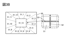
- FIG. 3B is a schematic diagram for explaining the configuration of the display control unit 50 of the semiconductor device 100.
- FIG. 3B shows, as an example, a configuration example of the drive circuit unit 51_13 having drive circuits 52, 53 for driving the pixel circuits 62 of the display area 61_13.
- the drive circuits 52 and 53 correspond to, for example, a source driver circuit and a gate driver circuit.
- the diagram shows a configuration in which the display area 61 and the display control unit 50 are each divided into 13 sections.
- One of the display regions 61 and one of the driver circuit units 51 are provided to overlap (see FIG. 3C).
- the display region 61_13 and the driver circuit unit 51_13 are provided to overlap.
- the driver circuit 52 of the driver circuit unit 51_13 is electrically connected to wiring for transmitting image data to the pixel circuit 62 of the display region 61_13.
- the driver circuit 53 of the driver circuit unit 51_13 is electrically connected to wiring for selecting the pixel circuit 62 to which the image data is to be transmitted, of the display region 61_13.
- the driver circuits 52 and 53 of the driver circuit unit 51_13 have a function of controlling the multiple pixel circuits 62 of the display region 61_13.
- the driver circuit units 51_1 to 51_12 have a function of controlling the pixel circuits 62 of the display regions 61_1 to 61_12, which are provided to overlap.
- the shapes of the display areas 61_1 to 61_12 other than the display area 61_13 are polygonal shapes other than rectangular shapes.
- the drive circuit unit 51 which is provided so as to overlap the polygonal display area 61, arranges the drive circuits 52 and 53 according to the shape of the display area 61. Since the drive circuit unit 51 is provided at a position where it overlaps the display area 61, the degree of freedom in arranging the drive circuits 52 and 53 can be increased.
- the display control unit 50 can be arranged at a position overlapping the display unit 60 having the display areas 61_1 to 61_13.
- the connection distance (wiring length) between the pixel circuit 62 in the display area 61 and the driver circuits 52 and 53 in the driver circuit unit 51 can be made extremely short.
- the wiring resistance and parasitic capacitance are reduced, so the time required for charging and discharging is shortened, and high-speed driving can be achieved.
- power consumption can be reduced.
- miniaturization and weight reduction can be achieved.
- the semiconductor device 100 has a configuration in which drive circuits 52, 53 are provided for each drive circuit section 51. Therefore, the display section 60 can be divided into display areas 61 corresponding to the drive circuit sections 51, and image data can be updated. For example, the image data can be updated only for display areas 61 in the display section 60 where a change has occurred in the image, and for display areas 61 where no change has occurred, an electric potential corresponding to the image data can be held in the pixel circuits 62, thereby stopping the operation of the drive circuit sections 51. As a result, the semiconductor device 100 can achieve reduced power consumption.
- the semiconductor device 100 can have a stacked structure of a display section 60 having a pixel circuit and a display control section 50 having a driver circuit, and therefore the aperture ratio (effective display area ratio) of the pixel can be extremely high.
- the aperture ratio of the pixel can be 40% or more and less than 100%, preferably 50% or more and 95% or less, and more preferably 60% or more and 95% or less.
- the pixel circuits can be arranged at an extremely high density, and the resolution of the pixel can be extremely high.
- pixels can be arranged at a resolution of 2000 ppi or more, preferably 3000 ppi or more, more preferably 5000 ppi or more, and even more preferably 6000 ppi or more, and 20000 ppi or less, or 30000 ppi or less.
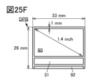
- the diagonal size of the display unit 60 can be 0.1 inches or more and 5.0 inches or less, preferably 0.5 inches or more and 2.0 inches or less, and more preferably 1 inch or more and 1.7 inches or less.
- the diagonal size of the display unit 60 can be 1.5 inches or close to 1.5 inches.
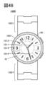
- FIG. 4A and 4B are diagrams for explaining an operation example of an electronic device 1000 including a semiconductor device 100.
- the display unit 60 of the semiconductor device 100 described above is applied to the display unit of the electronic device 1000. Note that, although an example in which the display unit 60 of the electronic device 1000 is rectangular is shown in FIG. 4A, the operation example of the electronic device 1000 described below can also be applied to a circular display unit 60 as shown in FIG. 4B.
- 4A and 4B are schematic diagrams of electronic device 1000 as viewed from the front side.
- 4A and 4B show the application of an analog clock face to display unit 60 having multiple display areas 61.
- 4A and 4B also show hour hand 1011, minute hand 1012, second hand 1013, and dial 1014 displayed on display unit 60. Second hand 1013 or dial 1014 is not necessarily required.
- dotted lines are used to show the boundaries of display areas 61 on display unit 60.
- 4A and 4B show the display area divided into 13 parts as described in FIG. 2A and 2B.
- the display area 61 shown in Figs. 4A and 4B is provided overlapping one of the multiple drive circuit units 51 as described in Figs. 2A and 2B, and the pixel circuits can be controlled for each display area 61. Therefore, the drive circuit of the drive circuit unit 51 can be paused or the image data can be updated (resumed) according to the image data for each display area 61.
- FIG. 5 is an example of a flowchart illustrating an example of the operation of the electronic device 1000.
- the computing device 10 acquires time data (step S11).
- the time data is data acquired by a timer or the like. Based on the time data, image data is generated for displaying an analog clock on the display unit 60.
- the image data supplied to the drive circuit unit 51 of the display control unit 50 is updated (step S12).
- the image data is updated for each display area 61 of the display unit 60, i.e., for each drive circuit unit 51 corresponding to the display area 61.
- the image data based on the time data is used to determine whether the display area 61 is a display area where the hour hand, minute hand, and second hand are displayed (step S13). If the second hand is not displayed, the design can be modified appropriately so that the display area 61 is determined to be a display area where the hour hand and minute hand are displayed. If the display area 61 is one where the hour hand, minute hand, and second hand are displayed based on the time data (YES), image data is sent to the drive circuit unit 51 corresponding to the display area 61, and the image in the display area 61 is updated based on the sent image data (step S14).
- step S13 if the display area 61 does not display the hour hand, minute hand, and second hand due to the time data (NO), the drive circuit of the drive circuit unit 51 corresponding to the display area 61 is paused (step S15).
- the pause operation includes stopping the supply of scanning signals from the drive circuit to the pixel circuits, stopping the supply of image data, etc. This pause operation reduces the frequency with which the drive circuit unit 51 supplies signals.
- the calculation device 10 After pausing the drive circuit of the drive circuit unit 51 in step S15, the calculation device 10 acquires time data (step S16). If the time data is acquired at a fixed interval, such as once per second if there is a second hand, or once per minute if there is no second hand, it is possible to periodically perform power gating of the calculation device 10, etc. This allows for low power consumption.
- the image data supplied to the drive circuit unit 51 of the display control unit 50 is updated (step S17).
- the image data is updated for each display area 61 of the display unit 60, i.e., for each drive circuit unit 51 corresponding to the display area 61.
- step S18 It is determined whether the display area 61 is a display area where the hour, minute, and second hands are displayed based on image data based on time data (step S18). If the display area 61 is one where the hour, minute, and second hands are displayed based on time data (YES), the drive circuit of the drive circuit unit 51 corresponding to the display area 61 is resumed (step S19), and image data is then sent to the drive circuit unit 51 corresponding to the display area 61, and the image of the display area 61 is updated based on the sent image data (step S14).
- the drive circuit of the drive circuit unit 51 corresponding to the display area 61 continues to be inactive, and the calculation device 10 performs step S16 to acquire time data and step S17 to update the image data.
- FIGS. 6A to 6F The state of the display unit 60 and the display control unit 50 in the electronic device 1000 based on the flowchart described in FIG. 5 will be specifically described with reference to FIGS. 6A to 6F.
- the boundaries of the display area 61 in the display unit 60 are illustrated using dotted lines.
- the display area is illustrated as being divided into 13 parts as described in FIGS. 2A and 2B. Therefore, in the description of FIGS. 6A to 6F, when specifying the position of the display area 61, it will be described as display areas 61_1 to 61_13. Similarly, when specifying the position of the drive circuit unit 51, it will be described as drive circuit units 51_1 to 51_13.
- FIG. 6A is a diagram showing the analog clock display on display unit 60 showing "1:28:54.”
- the hour hand display on display unit 60 is in display areas 61_2 and 61_13, as shown in FIG. 6B.
- the minute hand display on display unit 60 is in display areas 61_6, 61_7, and 61_13, as shown in FIG. 6B.
- the second hand display on display unit 60 is in display areas 61_12 and 61_13, as shown in FIG. 6B.
- the display areas in which image data is updated based on the time data are display areas 61_2, 61_6, 61_7, 61_12, and 61_13.
- the other display areas are display areas that only display the dial face, and are display areas in which image data is not updated. For this reason, the display areas in which the image data is not updated are shown with hatching in Figure 6B.
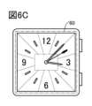
- FIG. 6C is a diagram showing how the analog clock on display unit 60 shows "3:07:10.”
- the hour hand on display unit 60 is displayed in display areas 61_4 and 61_13, as shown in FIG. 6D.
- the minute hand on display unit 60 is displayed in display areas 61_2, 61_3, and 61_13, as shown in FIG. 6D.
- the second hand on display unit 60 is displayed in display areas 61_3 and 61_13, as shown in FIG. 6D.
- the display areas in which image data is updated based on the time data are display areas 61_2, 61_3, 61_4, and 61_13.
- the other display areas are display areas that only display the dial face, and are display areas in which image data is not updated. For this reason, the display areas in which the image data is not updated are shown with hatching in Figure 6D.
- FIG. 6E is a diagram showing the analog clock display on display unit 60 showing "3:14:15.”
- the hour hand display on display unit 60 is in display areas 61_4 and 61_13, as shown in FIG. 6F.
- the minute hand display on display unit 60 is in display areas 61_4 and 61_13, as shown in FIG. 6F.
- the second hand display on display unit 60 is in display areas 61_4 and 61_13, as shown in FIG. 6F.
- the display areas in which image data is updated based on the time data are display areas 61_4 and 61_13.
- the other display areas are display areas that only display the dial face, and are display areas in which image data is not updated. For this reason, the display areas in which the image data is not updated are shown with hatching in Figure 6F.
- driver circuit portions 51 that drive multiple display areas 61 separately are arranged in an overlapping manner.
- the driver circuits can switch between pausing and resuming operation depending on whether image data is updated. Therefore, the electronic device 1000 including the semiconductor device 100 can achieve low power consumption.
- ⁇ Configuration Example of Semiconductor Device> 7 and 8 are block diagrams for explaining a configuration example of the logic circuit unit 31 included in the semiconductor device 100.
- the arithmetic device 10 the memory device 20, a bridge circuit 33, a power management unit (PMU) 34, a power supply circuit 35, a sensor control circuit 36, and a battery control circuit 37 are illustrated.
- PMU power management unit
- the computing device 10 includes, as an example, a CPU core 11, an L1 cache memory device 12, an L2 cache memory device 13, and a bus interface unit 14.
- the L1 cache memory device 12 may be called an instruction cache.
- the L2 cache memory device 13 may be called a data cache.
- the calculation device 10 corresponds to a circuit that processes image data, such as a CPU (Central Processing Unit).
- the calculation device 10 may also be called a CPU or a processor device.
- the CPU core 11 has multiple CPU cores.
- the CPU cores have a backup circuit 10M electrically connected to scan flip-flops.
- the L1 cache memory device 12 has a function of temporarily storing instructions to be executed by the CPU core 11.
- the L2 cache memory device 13 has a function of temporarily storing data to be processed by the CPU core 11 or data obtained by processing.
- the bus interface unit 14 may have a circuit configuration capable of transmitting and receiving signals such as data and addresses between the arithmetic device 10 and a bus for connecting other circuits within the semiconductor device 100.
- the scan flip-flop in the arithmetic device 10 is configured as a circuit having a Si transistor, i.e., a Si CMOS.
- the backup circuit 10M is configured to have an OS transistor.
- the backup circuit 10M having an OS transistor can function as an OS memory having a function of retaining charge for a long period of time by turning off the OS transistor.
- the scan flip-flop has a function of holding data held by the arithmetic device 10 and outputting it sequentially in response to a clock signal, etc.
- the scan flip-flop has a configuration in which it is electrically connected to the backup circuit 10M. This configuration makes it possible to output (back up) data held by the scan flip-flop to the backup circuit 10M, and to input (recover) data held by the backup circuit 10M to the scan flip-flop. Therefore, the semiconductor device 100 can significantly reduce sleep power (power during non-display periods) when the electronic device 1000 is in a sleep state, thereby improving convenience even with a small battery capacity.
- the OS transistor Since the band gap of the metal oxide is 2.5 eV or more, the OS transistor has a very small off-current.
- the off-current per 1 ⁇ m of channel width can be less than 1 ⁇ 10 ⁇ 20 A, less than 1 ⁇ 10 ⁇ 22 A, or less than 1 ⁇ 10 ⁇ 24 A at room temperature (25° C.) with a source-drain voltage of 3.5 V. Therefore, the amount of charge leaked from the retention node of the OS memory through the OS transistor is extremely small. Therefore, the OS memory can function as a nonvolatile memory circuit, which enables power gating of the computing device 10.
- Densely integrated semiconductor devices may generate heat when the circuits are operating. This heat increases the temperature of the transistor, which can change the characteristics of the transistor, causing a change in field-effect mobility or a decrease in operating frequency.
- OS transistors have higher heat resistance than Si transistors, so they are less likely to experience changes in field-effect mobility due to temperature changes and are also less likely to experience a decrease in operating frequency. Furthermore, OS transistors tend to maintain the characteristic that their drain current increases exponentially with respect to the gate-source voltage, even at high temperatures. Therefore, the use of OS transistors enables stable operation in high-temperature environments.
- Metal oxides that can be used in OS transistors include In oxide, Zn oxide, Zn-Sn oxide, Ga-Sn oxide, In-Ga oxide, In-Zn oxide, and In-M-Zn oxide (M is Ti, Ga, Y, Zr, La, Ce, Nd, Sn, or Hf).
- M is Ti, Ga, Y, Zr, La, Ce, Nd, Sn, or Hf.
- metal oxides using Ga as M are preferably used in OS transistors because they can be made into transistors with excellent electrical characteristics such as field effect mobility by adjusting the ratio of elements.
- oxides containing indium and zinc may contain one or more elements selected from aluminum, gallium, yttrium, copper, vanadium, beryllium, boron, silicon, titanium, iron, nickel, germanium, zirconium, molybdenum, lanthanum, cerium, neodymium, hafnium, tantalum, tungsten, magnesium, and the like.
- the computing device 10 can retain data even if the supply of power supply voltage is stopped by having the backup circuit 10M, which is the OS memory. This enables power gating of the computing device 10, and allows for a significant reduction in power consumption.
- the backup circuit 10M which is the OS memory, can be stacked with circuits composed of Si transistors, such as scan flip-flops, that the CPU core 11 has. Therefore, it can be arranged without increasing the circuit area.
- the memory device 20 functions as an on-chip memory.
- the on-chip memory is a memory device for storing data or programs input to and output from a circuit included in the semiconductor device 100, such as the arithmetic device 10.
- the memory device 20 has a memory cell array 21 and a peripheral circuit 22.
- the memory cell array 21 has memory cells 20M.
- Circuits applicable to the memory cells 20M include memories with Si transistors such as SRAM (Static RAM) and DRAM (Dynamic RAM), as well as memories with OS transistors such as DOSRAM or NOSRAM.
- DOSRAM registered trademark
- SRAM Static RAM
- DRAM Dynamic RAM
- OS transistors such as a semiconductor RAM
- NOSRAM is an abbreviation for "Dynamic Oxide Semiconductor RAM” and refers to a RAM with 1T (transistor) 1C (capacitor) type memory cells.
- DOSRAM is a memory that utilizes the low off-current of OS transistors.
- DOSRAM is a DRAM formed using OS transistors, and is a memory that temporarily stores information sent from the outside.
- the memory device 20 can be provided with memory cells 20M including OS transistors and peripheral circuits 22 including Si transistors (transistors having silicon in the channel formation region) in different stacked layers, so DOSRAM can reduce the overall circuit area.
- DOSRAM can also divide the memory cell array into smaller parts and arrange them efficiently.
- DOSRAM can also be configured to have OS transistors provided in multiple layers, allowing it to be configured to be stacked.
- the bus 39A is a bus for transmitting and receiving various signals at high speed between the arithmetic device 10, the memory device 20, and the PMU 34.
- an AMBA Advanced Microcontroller Bus Architecture
- AHB Advanced High-performance Bus
- the bus 39A is also a bus for transmitting various signals at high speed between the multiple drive circuit units 51_1 to 51_n of the display control unit 50.
- the circuits connected to the bus 39A of the logic circuit unit 31 may include an accelerator, a memory controller, a direct memory access controller, an interface circuit, or the like.
- the PMU 34 has a circuit configuration for controlling power gating of circuits such as the CPU core 11 of the arithmetic unit 10 of the semiconductor device 100.
- the power supply circuit 35 is a circuit for generating voltages used within the semiconductor device 100.
- Bus 39B is a bus for transmitting and receiving various signals between the sensor control circuit 36 and the battery control circuit 37 at low speed.
- an AMBA-APB Advanced Peripheral Bus
- Various signals are transmitted and received between bus 39A and bus 39B via bridge circuit 33.
- Circuits connected to bus 39B of logic circuit unit 31 may include an interrupt control circuit, an accelerator, an interface circuit, a timer circuit, a watchdog circuit, etc.
- the sensor control circuit 36 has a circuit configuration for transmitting and receiving data related to charging and discharging of the sensor 1002 outside the semiconductor device 100.
- the sensor control circuit 36 supplies the necessary power to the sensor 1002.
- the sensor control circuit 36 also receives input from the sensor 1002, converts it into a control signal, and outputs it to the arithmetic device 10 via the bus 39B or the like.
- the sensor control circuit 36 may perform error management of the sensor 1002, or may perform calibration processing of the sensor control circuit 36.
- the sensor control circuit 36 may be configured to include multiple control circuits for controlling the sensor 1002.
- the sensor 1002 has a function of acquiring one or more of information from a person's vision, hearing, touch, taste, and smell. More specifically, the sensor 1002 has at least one of the functions of detecting or measuring force, displacement, position, speed, acceleration, angular velocity, rotation speed, distance, light, magnetism, temperature, sound, time, electric field, current, voltage, power, radiation, humidity, inclination, vibration, odor, and infrared.
- an image sensor, a gyro sensor, an acceleration sensor, or a sensor that comes into contact with a part of the human body to measure heart rate, surface temperature, blood oxygen concentration, or the like can be applied.
- a sensor such as a three-axis gyro sensor or an acceleration sensor
- the functions of the electronic device 1000 can be switched on and off, thereby saving power.
- the battery control circuit 37 can manage the charge/discharge state of the battery 1003 outside the semiconductor device 100.
- the battery control circuit 37 may have, for example, a multi-channel power converter or inverter, a protection circuit, etc.
- the battery control circuit 37 also supplies power from the battery 1003 to the power supply circuit 35, which in turn supplies power to each component via a power supply line (not shown).
- the battery control circuit 37 has the function of receiving power supplied from the outside and charging the battery 1003.
- the battery control circuit 37 can control the charging operation of the battery 1003 depending on the charging state of the battery 1003.
- the battery control circuit 37 also preferably has a power saving function.
- the power saving function may include detecting that there has been no input of data or the like to the semiconductor device 100 for a certain period of time, and lowering the clock frequency of a clock signal generation circuit (not shown) that supplies a clock signal to the arithmetic device 10 or stopping the input of the clock signal, stopping the operation of the arithmetic device 10 itself, stopping the operation of the memory device 20, reducing the power supplied to each component to reduce power consumption, and the like.
- Such functions may be executed by the battery control circuit 37 alone or in conjunction with the arithmetic device 10.
- the battery 1003 may be, for example, a secondary battery such as a lithium ion battery, a solar cell, or the like.
- the battery 1003 may be provided with a protection circuit that prevents the battery 1003 from being overcharged or overdischarged.
- a battery may be referred to as a power storage device.
- a solar cell may be referred to as a photoelectric conversion device.
- the battery 1003 may also be a flexible battery. By making the battery 1003 flexible, the freedom of design of electronic devices can be increased.
- the semiconductor device 100 may have a control circuit in response to the operation of the operation unit 1004. Furthermore, in addition to the operation unit 1004, if the semiconductor device 100 is connected to a touch panel, the touch panel may also be configured to have a control circuit similar to the operation unit.
- the semiconductor device 100 may have a module (also called a communication module) having a function of communicating with the outside.
- the communication module may be provided with, for example, a high-frequency circuit (RF circuit) for transmitting and receiving RF signals.
- the high-frequency circuit is a circuit for converting between electromagnetic signals and electrical signals in a frequency band determined by the legislation of each country, and for communicating wirelessly with other communication devices using the electromagnetic signals.
- a practical frequency band is generally several tens of kHz to several tens of GHz.
- the high-frequency circuit connected to the antenna has a high-frequency circuit section corresponding to multiple frequency bands, and the high-frequency circuit section may be configured to have an amplifier, mixer, filter, DSP, RF transceiver, etc.
- the communication protocol or technology that can be used may be a communication standard defined by 3GPP (Third Generation Partnership Project) (registered trademark), such as LTE (Long Term Evolution) (registered trademark), LTE-Advanced corresponding to the fourth generation mobile communication system, the fifth generation mobile communication system (5G), or a standard corresponding to the sixth generation mobile communication system (6G), or a communication standard defined by IEEE (Institute of Electrical and Electronics Engineers) (registered trademark), such as Wi-Fi (registered trademark) or Bluetooth (registered trademark).
- 3GPP Third Generation Partnership Project
- LTE Long Term Evolution
- 5G Fifth Generation mobile communication system
- 6G sixth generation mobile communication system
- IEEE Institutee of Electrical and Electronics Engineers
- Wi-Fi registered trademark
- Bluetooth registered trademark
- FIG. 8 is a diagram showing a modified example of the block diagram of the semiconductor device 100 shown in FIG. 7.
- the block diagram of the semiconductor device 100S shown in FIG. 8 shows a configuration having a solar cell 1008 and a control circuit 38 for converting the power obtained by the solar cell 1008 in addition to the configuration of the semiconductor device 100 shown in FIG. 7.
- the solar cell 1008 for example, a silicon solar cell with crystalline silicon as a photoelectric conversion layer, or a solar cell with a tandem structure of a silicon solar cell and a perovskite solar cell can be used.
- a silicon solar cell with crystalline silicon as a photoelectric conversion layer or a solar cell with a tandem structure of a silicon solar cell and a perovskite solar cell can be used.
- an amorphous silicon solar cell, a CIGS (Cu-In-Ga-Se) type solar cell, an organic solar cell, or a perovskite solar cell can be used. Since the organic solar cell or the perovskite solar cell has high light transmittance, it can be provided overlapping the display unit 60.
- the control circuit 38 has a function of detecting the power generation state of the solar cell 1008. Depending on the power generation state, the control circuit 38 can control whether the generated power is used to drive the semiconductor device 100 or to charge the battery 1003.
- the electronic device 1000 By making the electronic device 1000 include a solar cell, the battery usage time can be extended, making it possible to provide a more convenient semiconductor device and an electronic device equipped with the semiconductor device.
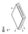
- the semiconductor device 100 shown in FIG. 9A has an element layer 40 on the element layer 30, and a sealing substrate 99 on the element layer 40.
- An element layer 90 (not shown) is provided between the sealing substrate 99 and the element layer 40.
- the semiconductor device 100 shown in FIG. 9B shows the element layer 30, element layer 40, element layer 90, sealing substrate 99, etc. shown in FIG. 9A separated from each other.
- the element layer 30 has a terminal portion 92.
- the element layer 30 has a calculation device 10, a memory device 20, and a display control unit 50 in the area where it overlaps with the element layer 40.
- the display control unit 50 has a plurality of drive circuit units 51 in which drive circuits are provided.
- the terminal portion 92 is electrically connected to flexible printed circuits (FPCs) and the like. Therefore, the element layer 40 and the sealing substrate 99 are not formed in the area that overlaps with the terminal portion 92.
- FPCs flexible printed circuits
- FIG. 1B illustrates the arithmetic device 10 and memory device 20 as the logic circuit section 31 of the element layer 30, other configurations may be used. For example, it may include all of the other configurations illustrated in FIG. 1A, or may include configurations other than these.
- the element layer 90 has a light-emitting device (not shown) such as an organic EL element.
- the light emission of the light-emitting device is controlled by a pixel circuit of a sub-pixel (sub-pixel) for displaying color. Therefore, the element layer 90 can also be considered as part of the display unit 60.
- the term “element” may sometimes be referred to as "device.”
- a display element and a light-emitting element may be referred to as a display device and a light-emitting device, respectively.
- the element layer 30 has a transistor 56 having silicon in a semiconductor layer 58 having a channel formation region.
- the wiring electrically connecting the arithmetic device 10, memory device 20, and display control unit 50 can be shortened. This shortens the charge and discharge time of the wiring that transmits control signals for the arithmetic device 10 to control the display control unit 50, thereby reducing power consumption.
- the element layer 40 has a transistor 66 having a metal oxide in a semiconductor layer 68 having a channel formation region.
- OS transistors as the transistors in the pixel circuits provided in the display unit 60, a potential corresponding to the image data signal can be held in the pixel circuit, so that a still image can be displayed without updating the image data.
- the arithmetic unit 10 and the memory unit 20 may be disposed in the display control unit 50.
- the arithmetic unit 10 and the memory unit 20 may be provided in a distributed manner in an area other than the area in which the drive circuits 52 and 53 are disposed (see FIG. 9C). With this configuration, when the area of the drive circuit unit 51 in which the drive circuits 52 and 53 are disposed is larger than the area in which the drive circuits 52 and 53 are disposed, the remaining space can be used to efficiently arrange the circuits.
- the backup circuit 10M of the arithmetic device 10 and the memory cell 20M of the memory device 20 it is preferable to provide the backup circuit 10M of the arithmetic device 10 and the memory cell 20M of the memory device 20.
- the backup circuit 10M and the memory cell 20M are configured to use transistors provided in the same element layer as the pixel circuit 62. It is preferable to arrange the backup circuit 10M and the memory cell 20M provided in the element layer 40 in a position that overlaps with the arithmetic device 10 and the memory device 20 provided in the element layer 30, as shown in FIG. 10A.
- the backup circuit 10M can be arranged directly above the scan flip-flop of the arithmetic device 10. This allows the wiring for electrically connecting the scan flip-flop and the backup circuit 10M to be shorter. This reduces the wiring resistance and parasitic capacitance, and increases the operating speed of the semiconductor device 100. In addition, the power consumption of the semiconductor device 100 is reduced.
- the backup circuit 10M of the computing device 10 and the memory cell 20M of the memory device 20 can be disposed on the outer periphery of the display unit 60, so that the semiconductor device 100 can be disposed in an area covered by the housing 1001 of the electronic device 1000. Therefore, the backup circuit 10M of the computing device 10 and the memory cell 20M of the memory device 20 can be disposed in an area in the element layer 40 where the display unit 60 is not disposed, so that the backup circuit 10M and the memory cell 20M can be disposed without degrading the display quality of the display unit 60.
- the element layer 40 having the transistor 66 may be multiple element layers, for example, element layers 40_1 and 40_2 as shown in FIG. 10B.
- element layers 40_1 and 40_2 can be used to stack element layers having transistors with different transistor characteristics.
- element layers 40_1 and 40_2 can be used to stack element layers having transistors with different transistor shapes.
- element layers 40_1 and 40_2 can be used to stack element layers having transistors with different transistor sizes, such as the channel length and channel width of the transistor.
- the backup circuit 10M of the computing device 10 and the memory cell 20M of the memory device 20 are provided in the element layer 40_1 above the element layer 30, and the pixel circuit, i.e., the display unit 60 having a display area 61, is provided in the element layer 40_2 below the element layer 90.
- the element layer 40_1 can be an element layer having transistors with increased drive frequency to improve the performance of the backup circuit 10M and the memory cell 20M
- the element layer 40_2 can be an element layer having transistors with increased voltage resistance to improve the performance of the pixel circuit. Therefore, the semiconductor device 100 can be a semiconductor device that can achieve high performance.
- FIG. 11A is a diagram showing a different configuration of the design of the display unit 60 from that described in FIG. 4A.
- FIG. 11A shows a configuration in which a digital clock is displayed in the display area 61_13 of the display unit 60.
- ⁇ Example of pixel circuit configuration> 12A and 12B show a configuration example of a pixel circuit 62 and a light-emitting device 91 connected to the pixel circuit 62.
- Fig. 12A is a diagram showing the connection of each element
- Fig. 12B is a diagram showing a schematic hierarchical relationship between an element layer 30 having drive circuits 52 and 53, an element layer 40 having a pixel circuit 62, and an element layer 90 having a light-emitting device 91.
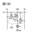
- the pixel circuit 62 shown as an example in FIG. 12A and FIG. 12B includes a transistor 63A, a transistor 63B, a transistor 63C, and a capacitor 64.
- the transistors 63A, 63B, and 63C can be OS transistors.
- Each of the OS transistors 63A, 63B, and 63C preferably includes a backgate electrode.
- the backgate electrode can be configured to receive the same signal as the gate electrode, or the backgate electrode can be configured to receive a signal different from the gate electrode.
- the light-emitting device 91 has a first electrode electrically connected to the first electrode of the transistor 63B, and a second electrode electrically connected to the wiring VCOM.
- the wiring VCOM is a wiring for providing a potential for supplying a current to the light-emitting device 91.
- the intensity of the light emitted by the light-emitting device 91 to be controlled according to the image signal applied to the gate electrode of transistor 63B.
- the reference potential of the wiring V0 applied via transistor 63C can suppress variations in the gate-source voltage of transistor 63B.
- the light-emitting device described in one embodiment of the present invention refers to a self-emitting display element such as an organic EL element (also called an OLED (Organic Light Emitting Diode)).
- the light-emitting device electrically connected to the pixel circuit can be a self-emitting light-emitting device such as an LED (Light Emitting Diode), a micro LED, a QLED (Quantum-dot Light Emitting Diode), a semiconductor laser, etc.
- transistor 63B By simultaneously turning on transistors 63C and 63D, the source and gate of transistor 63B are at the same potential, and transistor 63B can be turned off. This makes it possible to forcibly cut off the current flowing through light-emitting device 91.
- This type of pixel circuit is suitable for use in a display method in which display periods and off periods are alternated.
- the PMU 34 In response to interrupt signals (Interrupts) input from the outside and signals such as the signal SLEEP1 issued by the arithmetic unit 10, the PMU 34 generates a clock signal GCLK1 and various PG (power gating) control signals (PG control signals).
- the clock signal GCLK1 and the PG control signals are input to the arithmetic unit 10.
- the PG control signals control the power switches 15A to 15C and the flip-flop 16.
- Voltage VDDD and VDD1 are drive voltages for CMOS circuits. Voltage VDD1 is lower than voltage VDDD and is the drive voltage in the sleep state. Voltage VDDH is the drive voltage for OS transistors and is higher than voltage VDDD.
- Signal SCE is a scan enable signal and is generated by PMU 34.
- PMU 34 generates signals BK and RC.
- Level shifter 15D shifts the levels of signals BK and RC to generate signals BKH and RCH.
- Signals BK and RC are a backup signal and a recovery signal.
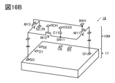
- the backup circuit 10M has nodes SD_IN, SN11, transistors M11 to M13, and a capacitance C11.
- the backup circuit 10M can be stacked on a scan flip-flop 17 that is configured as a silicon CMOS circuit.
- the backup circuit 10M has a much smaller number of elements than the scan flip-flop 17, there is no need to change the circuit configuration and layout of the scan flip-flop 17 in order to stack the backup circuit 10M.
- the backup circuit 10M is a highly versatile backup circuit.
- the backup circuit 10M can be provided within the region in which the scan flip-flop 17 is formed, the area overhead of the flip-flop 16 can be reduced to zero even when the backup circuit 10M is incorporated. Therefore, by providing the backup circuit 10M in the flip-flop 16, power gating of the CPU core 11 becomes possible. Since little energy is required for power gating, the CPU core 11 can be power gated with high efficiency.
- the low power consumption state of the CPU core 11 can be set to, for example, a clock gating state, a power gating state, or a pause state (non-operation).
- the PMU 34 selects the low power consumption mode of the CPU core 11 based on an interrupt signal, the signal SLEEP1, etc. For example, when transitioning from a normal operating state to a clock gating state, the PMU 34 stops generating the clock signal GCLK1.
- the PMU 34 when transitioning from a normal operating state to a hibernation state (non-operating state), the PMU 34 performs voltage and/or frequency scaling. For example, when performing voltage scaling, the PMU 34 turns off the power switch 15A and turns on the power switch 15B to input the voltage VDD1 to the CPU core 11.
- the voltage VDD1 is a voltage that does not cause the data in the scan flip-flop 17 to be lost.
- the PMU 34 reduces the frequency of the clock signal GCLK1.
- the normal operation state (Normal Operation) is established.
- the power switch 15A is on, and the voltage VDDD is input to the CPU core 11.
- the scan flip-flop 17 operates normally.
- the level shifter 15D does not need to operate, so the power switch 15C is off, and the signals SCE, BK, and RC are "L”. Since the node SE is "L”, the scan flip-flop 17 stores the data of the node D1.
- the node SN11 of the backup circuit 10M is "L”.
- the PMU 34 sets signals PSE2 and BK to "L” at time t2, and sets signal PSE0 to "L” at time t3. At time t3, the state of the CPU core 11 transitions to a power gating state. Note that signal PSE0 may be lowered at the same time that signal BK is lowered.
- PMU34 sets signals PSE2, SCE, and RC to "L" and the recovery operation ends.
- the memory device 20 shown in FIG. 18A has a memory cell array 21 and peripheral circuits 22.
- the peripheral circuits 22 include a control circuit 24, a row circuit 25, a column circuit 26, and an input/output circuit 27.
- the memory cell array 21 has memory cells 23, read word lines RWL, write word lines WWL, read bit lines RBL, write bit lines WBL, wiring SL, and wiring BGL. Note that the read word lines RWL and write word lines WWL may be referred to as word lines RWL and word lines WWL, respectively.
- the read bit lines RBL and write bit lines WBL may be referred to as bit lines RBL and bit lines WBL, respectively.
- the control circuit 24 performs overall control of the memory device 20 and writes and reads data.
- the control circuit 24 processes command signals (e.g., chip enable signals, write enable signals, etc.) from the outside and generates control signals for the other circuits in the peripheral circuit 22.
- command signals e.g., chip enable signals, write enable signals, etc.
- the row circuit 25 has a function of selecting a row to be accessed.
- the row circuit 25 has a row decoder and a word line driver.
- the column circuit 26 has a function of precharging the bit lines WBL and RBL, a function of writing data to the bit line WBL, a function of amplifying data on the bit line RBL, a function of reading data from the bit line RBL, etc.
- the input/output circuit 27 has a function of holding write data, a function of holding read data, etc.
- FIG. 18B shows an example of the circuit configuration of memory cell 23.
- memory cell 23 is a two-transistor (2T) gain cell.
- Memory cell 23 has transistors MW1 and MR1, and a capacitance element CS1.
- Transistor MW1 is a write transistor
- transistor MR1 is a read transistor.
- the back gates of transistors MW1 and MR1 are electrically connected to wiring BGL.
- the read transistor is an OS transistor
- the memory cell 23 does not consume power to retain data. Therefore, the memory cell 23 is a low-power memory cell capable of retaining data for a long period of time, and the memory device 20 can be used as a non-volatile storage device.
- the OS transistor and the capacitance can be stacked on the Si transistor. Therefore, the memory cell array 21 can be stacked on the peripheral circuit 22, and the integration density of the memory cell array 21 can be improved.
- Memory cell 23A shown in FIG. 19A is a 3T type gain cell, and has transistors MW2, MR2, MS2, and a capacitance element CS2.
- Transistors MW2, MR2, and MS2 are a write transistor, a read transistor, and a selection transistor, respectively.
- the back gates of transistors MW2, MR2, and MS2 are electrically connected to wiring BGL.
- Memory cell 23A is electrically connected to word lines RWL, WWL, bit lines RBL, WBL, capacitance line CDL, and power line PL2. For example, voltage GND (low-level power supply voltage) is input to capacitance line CDL and power line PL2.
- voltage GND low-level power supply voltage
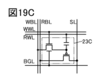
- FIGS. 19B and 19C show other configuration examples of a 2T type gain cell.
- the read transistor is an n-channel type Si transistor.
- the read transistor is a p-channel type Si transistor.
- the transistors in the memory cell may be a combination of OS transistors and Si transistors.
- FIGS. 19D and 19E show other configuration examples of a 3T type gain cell.
- the read transistor and select transistor are composed of n-channel type Si transistors.
- the read transistor and select transistor are composed of p-channel type Si transistors.
- voltage VDDD is input to power supply line PL2.
- bit line RBL and bit line WBL may be provided.
- FIG. 19F shows an example of a 1T1C (capacitor) type memory cell.
- Memory cell 23F shown in FIG. 19F is electrically connected to a word line WL, a bit line BL, a capacitance line CDL, and a wiring BGL.
- Memory cell 23F has a transistor MW3 and a capacitance element CS3. The back gate of transistor MW3 is electrically connected to the wiring BGL.
- the circuit configuration of the memory cell 20M of the memory device 20 can be a circuit configuration composed of only OS transistors, or a circuit configuration in which OS transistors are combined with Si transistors.
- the power consumed when the electronic device 1000 is in a sleep state can be significantly reduced, and convenience can be improved even if the battery capacity is small. As a result, the weight of the electronic device can be reduced.
- Embodiment 2 In this embodiment, a structural example of a transistor that can be used for the element layer 40 of the semiconductor device 100 described in the above embodiment 1 will be described. In particular, in this embodiment, a structural example of a transistor that can be used as an OS transistor will be described.
- FIG. 20A to 20C show an example of a semiconductor device (e.g., a pixel circuit or a driving circuit) including a transistor MTCK.
- FIG. 20A shows a schematic plan view of the transistor MTCK.
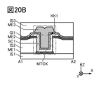
- FIG. 20B is a schematic cross-sectional view corresponding to the portion of the dashed line A1-A2 shown in FIG. 20A, and is also a schematic cross-sectional view of the transistor MTCK.
- FIG. 20C is a schematic cross-sectional view corresponding to the portion of the dashed line A3-A4 shown in FIG. 20A, and is also a schematic cross-sectional view of the transistor MTCK.
- Tantalum nitride, titanium nitride, nitrides containing titanium and aluminum, nitrides containing tantalum and aluminum, ruthenium oxide, ruthenium nitride, oxides containing strontium and ruthenium, and oxides containing lanthanum and nickel are preferred because they are conductive materials that are difficult to oxidize, or materials that maintain their conductivity even when they absorb oxygen.
- the conductor may be, for example, a semiconductor with high electrical conductivity, such as polycrystalline silicon containing an impurity element (e.g., phosphorus or arsenic), or a silicide (e.g., nickel silicide).
- the element M is preferably one or more of aluminum, gallium, yttrium, and tin. Furthermore, it is more preferable that the element M contains one or both of gallium and tin.
- the semiconductor SC1 is a metal oxide that functions as an oxide semiconductor
- the microwave treatment refers to a treatment using a device having a power source that generates high-density plasma using microwaves, for example.
- a composition close thereto includes a range of ⁇ 30% of the desired atomic ratio.
- an insulator GI1 is provided on the semiconductor SC1. Specifically, in a plan view, the insulator GI1 is positioned so as to overlap above the channel formation region included in the semiconductor SC1. The insulator GI1 functions as a gate insulating film in the transistor MTCK.
- the transistor MTCK shown in Figures 20A to 20C the conductor ME1 functioning as either the source or the drain is located below the insulator IS2, which serves as the interlayer film, and the conductor ME2 functioning as the other of the source or the drain is located above the insulator IS2. Therefore, the transistor MTCK is configured such that each channel formation region is provided along the opening of the insulator IS2.
- the formation area of the transistor can be made smaller than when the channel formation region of the transistor is provided along the X-Y plane. Therefore, by forming a circuit using the transistor MTCK, the area of the circuit can be made smaller. As a result, it is possible to reduce the size of a semiconductor device or display device that includes the circuit.
- the width H of conductor ME2_S and conductor ME2_D is smaller than the maximum width D of opening KK1.
- the circumferential direction of opening KK1 corresponds to the channel length direction L of transistor MTCK2.
- semiconductor SC1 since semiconductor SC1 has an annular shape, there are two types of current paths (i.e., channels) from conductor ME2_S to conductor ME2_D. Note that semiconductor SC1 does not necessarily have to have an annular shape, and may be configured to be in contact with both conductor ME2_S and conductor ME2_D.
- the transistor 300d has an element isolation layer 312, a conductor 316, an insulator 315, an insulator 317, a semiconductor region 313 formed of a part of the substrate 310, and a low-resistance region 314a and a low-resistance region 314b that function as a source region or a drain region. Therefore, the transistor 300d is a Si transistor. Note that FIG. 22 shows a configuration in which one of the source and drain of the transistor 300d is electrically connected to the conductor 330, the conductor 356, and the conductor 514 described later via the conductor 328 described later, but the electrical connection configuration of the semiconductor device of one embodiment of the present invention is not limited to this.
- the semiconductor device of one embodiment of the present invention may have a configuration in which, for example, the gate of the transistor 300d is electrically connected to the conductor 514 via the conductor 328.
- a conductor 328 is embedded in the insulator 320 and the insulator 322, and connects to the transistor MTCK and the like that are provided above the insulator 322.
- the conductor 328 functions as a plug or wiring.
- the conductor 328 can be made of a material that can be used for the conductor MPG described above.
- insulators having the function of suppressing the permeation of impurities such as water and hydrogen and oxygen may be, for example, metal oxides such as aluminum oxide, magnesium oxide, gallium oxide, germanium oxide, yttrium oxide, zirconium oxide, lanthanum oxide, neodymium oxide, hafnium oxide, and tantalum oxide.
- insulators having the function of suppressing the permeation of impurities such as water and hydrogen and oxygen may be, for example, oxides containing aluminum and hafnium (hafnium aluminate).
- materials such as silicon oxide, silicon oxynitride, and silicon oxide having vacancies are preferable because they can easily form a region containing oxygen that is desorbed by heating.
- a resin can be used for the insulator 581.
- the material that can be used for the insulator 581 may be an appropriate combination of the above-mentioned materials.
- the materials for each plug and wiring can be one or more conductive materials selected from metal materials, alloy materials, metal nitride materials, and metal oxide materials, either in a single layer or in a laminated form. It is preferable to use a high melting point material such as tungsten or molybdenum that has both heat resistance and conductivity, and tungsten is preferably used. Alternatively, it is preferable to form the wiring from a low resistance conductive material such as aluminum or copper. By using a low resistance conductive material, the wiring resistance can be reduced.
- a conductive material that is light-transmitting and light-reflective for the conductors 129a to 129c which are the upper electrodes (common electrodes)
- a conductive material that is light-reflective for the conductors 112a to 112c and conductors 126a to 126c which are the lower electrodes (pixel electrodes).
- the first layer 113a, the second layer 113b, and the third layer 113c have a clear distinction between the top and side surfaces.
- one side surface of the first layer 113a and one side surface of the second layer 113b are arranged opposite each other. This is the same for any combination of the first layer 113a, the second layer 113b, and the third layer 113c.
- various types of curing adhesives can be used, such as ultraviolet-curing photocuring adhesives, reaction-curing adhesives, heat-curing adhesives, and anaerobic adhesives.
- these adhesives include epoxy resins, acrylic resins, silicone resins, phenolic resins, polyimide resins, imide resins, PVC (polyvinyl chloride) resins, PVB (polyvinyl butyral) resins, and EVA (ethylene vinyl acetate) resins.
- epoxy resins with low moisture permeability are preferred.
- Two-part mixed resins may also be used.
- An adhesive sheet may also be used.
- Electronic devices can have a variety of functions. For example, they can have a function to display various information (still images, videos, text images, etc.) on a display unit, a touch panel function, a function to display a calendar, date or time, etc., a function to execute various software (programs), wireless communication means, a function to read out programs or data recorded on a recording medium, etc.
- the content described in one embodiment can be applied to, combined with, or replaced with another content described in that embodiment (or even a part of the content) and/or the content described in one or more other embodiments (or even a part of the content).
- the channel length refers to, for example, the distance between the source and drain in the region where the semiconductor (or the portion of the semiconductor through which current flows when the transistor is on) and the gate overlap in a top view of the transistor, or in the region where the channel is formed.
Landscapes
- Engineering & Computer Science (AREA)
- Physics & Mathematics (AREA)
- General Physics & Mathematics (AREA)
- Computer Hardware Design (AREA)
- Theoretical Computer Science (AREA)
- Thin Film Transistor (AREA)
- Control Of Indicators Other Than Cathode Ray Tubes (AREA)
Priority Applications (2)
| Application Number | Priority Date | Filing Date | Title |
|---|---|---|---|
| JP2024563763A JPWO2024127199A1 (https=) | 2022-12-16 | 2023-12-11 | |
| US19/134,806 US20260073863A1 (en) | 2022-12-16 | 2023-12-11 | Electronic device |
Applications Claiming Priority (2)
| Application Number | Priority Date | Filing Date | Title |
|---|---|---|---|
| JP2022-200779 | 2022-12-16 | ||
| JP2022200779 | 2022-12-16 |
Publications (1)
| Publication Number | Publication Date |
|---|---|
| WO2024127199A1 true WO2024127199A1 (ja) | 2024-06-20 |
Family
ID=91485102
Family Applications (1)
| Application Number | Title | Priority Date | Filing Date |
|---|---|---|---|
| PCT/IB2023/062447 Ceased WO2024127199A1 (ja) | 2022-12-16 | 2023-12-11 | 電子機器 |
Country Status (3)
| Country | Link |
|---|---|
| US (1) | US20260073863A1 (https=) |
| JP (1) | JPWO2024127199A1 (https=) |
| WO (1) | WO2024127199A1 (https=) |
Citations (5)
| Publication number | Priority date | Publication date | Assignee | Title |
|---|---|---|---|---|
| JP2014194540A (ja) * | 2013-02-28 | 2014-10-09 | Semiconductor Energy Lab Co Ltd | 画像情報の処理および表示方法、プログラム、情報処理装置 |
| JP2018025777A (ja) * | 2016-08-03 | 2018-02-15 | 株式会社半導体エネルギー研究所 | 表示装置および電子機器 |
| JP2018055097A (ja) * | 2016-09-23 | 2018-04-05 | 株式会社半導体エネルギー研究所 | 表示装置および電子機器 |
| CN109493793A (zh) * | 2019-01-14 | 2019-03-19 | 京东方科技集团股份有限公司 | 显示装置的控制方法、可穿戴装置 |
| WO2022118141A1 (ja) * | 2020-12-06 | 2022-06-09 | 株式会社半導体エネルギー研究所 | 表示装置、および表示補正システム |
-
2023
- 2023-12-11 JP JP2024563763A patent/JPWO2024127199A1/ja active Pending
- 2023-12-11 US US19/134,806 patent/US20260073863A1/en active Pending
- 2023-12-11 WO PCT/IB2023/062447 patent/WO2024127199A1/ja not_active Ceased
Patent Citations (5)
| Publication number | Priority date | Publication date | Assignee | Title |
|---|---|---|---|---|
| JP2014194540A (ja) * | 2013-02-28 | 2014-10-09 | Semiconductor Energy Lab Co Ltd | 画像情報の処理および表示方法、プログラム、情報処理装置 |
| JP2018025777A (ja) * | 2016-08-03 | 2018-02-15 | 株式会社半導体エネルギー研究所 | 表示装置および電子機器 |
| JP2018055097A (ja) * | 2016-09-23 | 2018-04-05 | 株式会社半導体エネルギー研究所 | 表示装置および電子機器 |
| CN109493793A (zh) * | 2019-01-14 | 2019-03-19 | 京东方科技集团股份有限公司 | 显示装置的控制方法、可穿戴装置 |
| WO2022118141A1 (ja) * | 2020-12-06 | 2022-06-09 | 株式会社半導体エネルギー研究所 | 表示装置、および表示補正システム |
Also Published As
| Publication number | Publication date |
|---|---|
| US20260073863A1 (en) | 2026-03-12 |
| JPWO2024127199A1 (https=) | 2024-06-20 |
Similar Documents
| Publication | Publication Date | Title |
|---|---|---|
| JP7389207B2 (ja) | 半導体装置 | |
| JP6488124B2 (ja) | 半導体装置 | |
| JP2015195365A (ja) | 半導体装置 | |
| JP2024019141A (ja) | 半導体装置、及び、半導体装置の作製方法 | |
| JP2017017320A (ja) | 半導体装置の作製方法 | |
| JP7577676B2 (ja) | 表示装置 | |
| WO2024141884A1 (ja) | 半導体装置、及び電子機器 | |
| WO2024127199A1 (ja) | 電子機器 | |
| WO2024241187A1 (ja) | 半導体装置 | |
| WO2024201259A1 (ja) | 半導体装置、及び、半導体装置の作製方法 | |
| WO2024189456A1 (ja) | 半導体装置、及び半導体装置の作製方法 | |
| WO2024116045A1 (ja) | 電子機器 | |
| JP7813726B2 (ja) | 発光素子、表示装置、および電子機器 | |
| US20250248216A1 (en) | Semiconductor device | |
| WO2024189455A1 (ja) | 半導体装置 | |
| WO2025196595A1 (ja) | 半導体装置 | |
| WO2025196598A1 (ja) | 半導体装置 | |
| CN117941066A (zh) | 电子装置及显示系统 | |
| JP2025109687A (ja) | 半導体装置 | |
| WO2025149872A1 (ja) | 半導体装置 | |
| WO2024154036A1 (ja) | 半導体装置 | |
| WO2024134442A1 (ja) | 半導体装置 | |
| WO2024236396A1 (ja) | 半導体装置、記憶装置、半導体装置の作製方法 | |
| WO2024224246A1 (ja) | 半導体装置、及び、半導体装置の作製方法 | |
| WO2024246718A1 (ja) | 半導体装置、及び、半導体装置の作製方法 |
Legal Events
| Date | Code | Title | Description |
|---|---|---|---|
| 121 | Ep: the epo has been informed by wipo that ep was designated in this application |
Ref document number: 23902906 Country of ref document: EP Kind code of ref document: A1 |
|
| WWE | Wipo information: entry into national phase |
Ref document number: 2024563763 Country of ref document: JP |
|
| NENP | Non-entry into the national phase |
Ref country code: DE |
|
| 122 | Ep: pct application non-entry in european phase |
Ref document number: 23902906 Country of ref document: EP Kind code of ref document: A1 |