WO2024122607A1 - アンテナ装置、および電子機器 - Google Patents
アンテナ装置、および電子機器 Download PDFInfo
- Publication number
- WO2024122607A1 WO2024122607A1 PCT/JP2023/043793 JP2023043793W WO2024122607A1 WO 2024122607 A1 WO2024122607 A1 WO 2024122607A1 JP 2023043793 W JP2023043793 W JP 2023043793W WO 2024122607 A1 WO2024122607 A1 WO 2024122607A1
- Authority
- WO
- WIPO (PCT)
- Prior art keywords
- coil
- antenna device
- electrode
- antenna
- conductor pattern
- Prior art date
- Legal status (The legal status is an assumption and is not a legal conclusion. Google has not performed a legal analysis and makes no representation as to the accuracy of the status listed.)
- Ceased
Links
Images


Classifications
-
- H—ELECTRICITY
- H01—ELECTRIC ELEMENTS
- H01Q—ANTENNAS, i.e. RADIO AERIALS
- H01Q13/00—Waveguide horns or mouths; Slot antennas; Leaky-waveguide antennas; Equivalent structures causing radiation along the transmission path of a guided wave
- H01Q13/10—Resonant slot antennas
- H01Q13/106—Microstrip slot antennas
-
- H—ELECTRICITY
- H01—ELECTRIC ELEMENTS
- H01Q—ANTENNAS, i.e. RADIO AERIALS
- H01Q13/00—Waveguide horns or mouths; Slot antennas; Leaky-waveguide antennas; Equivalent structures causing radiation along the transmission path of a guided wave
- H01Q13/10—Resonant slot antennas
-
- H—ELECTRICITY
- H01—ELECTRIC ELEMENTS
- H01F—MAGNETS; INDUCTANCES; TRANSFORMERS; SELECTION OF MATERIALS FOR THEIR MAGNETIC PROPERTIES
- H01F17/00—Fixed inductances of the signal type
-
- H—ELECTRICITY
- H01—ELECTRIC ELEMENTS
- H01F—MAGNETS; INDUCTANCES; TRANSFORMERS; SELECTION OF MATERIALS FOR THEIR MAGNETIC PROPERTIES
- H01F27/00—Details of transformers or inductances, in general
-
- H—ELECTRICITY
- H01—ELECTRIC ELEMENTS
- H01F—MAGNETS; INDUCTANCES; TRANSFORMERS; SELECTION OF MATERIALS FOR THEIR MAGNETIC PROPERTIES
- H01F27/00—Details of transformers or inductances, in general
- H01F27/28—Coils; Windings; Conductive connections
- H01F27/29—Terminals; Tapping arrangements for signal inductances
-
- H—ELECTRICITY
- H01—ELECTRIC ELEMENTS
- H01Q—ANTENNAS, i.e. RADIO AERIALS
- H01Q5/00—Arrangements for simultaneous operation of antennas on two or more different wavebands, e.g. dual-band or multi-band arrangements
- H01Q5/30—Arrangements for providing operation on different wavebands
- H01Q5/307—Individual or coupled radiating elements, each element being fed in an unspecified way
- H01Q5/342—Individual or coupled radiating elements, each element being fed in an unspecified way for different propagation modes
- H01Q5/35—Individual or coupled radiating elements, each element being fed in an unspecified way for different propagation modes using two or more simultaneously fed points
-
- H—ELECTRICITY
- H01—ELECTRIC ELEMENTS
- H01Q—ANTENNAS, i.e. RADIO AERIALS
- H01Q7/00—Loop antennas with a substantially uniform current distribution around the loop and having a directional radiation pattern in a plane perpendicular to the plane of the loop
-
- H—ELECTRICITY
- H01—ELECTRIC ELEMENTS
- H01Q—ANTENNAS, i.e. RADIO AERIALS
- H01Q1/00—Details of, or arrangements associated with, antennas
- H01Q1/12—Supports; Mounting means
- H01Q1/22—Supports; Mounting means by structural association with other equipment or articles
Definitions
- This disclosure relates to an antenna device and an electronic device.
- Patent Document 1 JP 09-74312 A
- slot antennas are not suitable as built-in antennas in electronic devices that are required to operate in multiple frequency bands.
- the objective of this disclosure is to provide an antenna device and electronic device that widens the available frequency band.
- An antenna device includes a plate-shaped conductor having an opening, a first excitation electrode and a second excitation electrode arranged at positions corresponding to the opening, a first coil having one end electrically connected to the first excitation electrode and the other end connected to a power supply circuit, and a second coil having one end electrically connected to the second excitation electrode.
- the first coil and the second coil are arranged in positions where they are magnetically coupled.
- An electronic device includes the antenna device described above, a power supply circuit that supplies power to the first excitation electrode, and a housing that houses the antenna device and the power supply circuit.
- a first excitation electrode and a second excitation electrode which are arranged at positions corresponding to the opening, are connected to a first coil and a second coil, which are magnetically coupled, respectively, so that a resonance point can be added to widen the usable frequency band.
- FIG. 1 is a schematic diagram of an electronic device including an antenna device according to a first embodiment. 2 is an enlarged view of a portion of the antenna device according to the first embodiment.
- FIG. 1 is a schematic cross-sectional view of an antenna device according to a first embodiment. 1 is an equivalent circuit diagram of an antenna device according to a first embodiment. 5 is a diagram showing frequency characteristics of the reflection coefficient of the antenna device according to the first embodiment;
- FIG. 2 is a diagram showing a Smith chart of the antenna device according to the first embodiment.
- FIG. 13 is a schematic diagram of a comparative antenna device.
- FIG. 13 is a diagram showing frequency characteristics of the reflection coefficient of a comparative antenna device.
- FIG. 13 is a diagram showing a Smith chart of a comparative antenna device.
- FIG. 2 is a perspective view of an antenna coupling element according to the first embodiment.
- FIG. 2 is a plan view of an antenna coupling element according to the first embodiment.
- FIG. 2 is a first exploded plan view showing the configuration of an antenna coupling element according to the first embodiment.
- 4 is a second exploded plan view showing the configuration of the antenna coupling element according to the first embodiment.
- FIG. FIG. 13 is a schematic diagram of another comparative antenna device.
- FIG. 13 is a diagram showing frequency characteristics of the reflection coefficient of another comparative antenna device.
- FIG. 13 is a diagram showing a Smith chart of another comparative antenna device.
- FIG. 13 is a schematic diagram of yet another comparative antenna device.
- FIG. 13 is a diagram showing frequency characteristics of the reflection coefficient of yet another comparative antenna device.
- FIG. 13 is a diagram showing frequency characteristics of the reflection coefficient of yet another comparative antenna device.
- FIG. 13 is a diagram showing a Smith chart of yet another comparative antenna device.
- 13 is a diagram showing frequency characteristics of the reflection coefficient of an antenna device in which the capacitance value of a capacitive element is changed.
- 13 is a diagram showing a Smith chart of an antenna device in which the capacitance value of a capacitive element is changed.
- FIG. FIG. 11 is a cross-sectional view of an antenna device according to a modified example. 11 is a schematic diagram of an electronic device including an antenna device according to a second embodiment.
- FIG. 13 is a diagram showing frequency characteristics of the reflection coefficient of the antenna device according to the second embodiment.
- FIG. 13 is a diagram showing the antenna efficiency of the antenna device according to the second embodiment.
- FIG. 13 is a schematic diagram of an electronic device including an antenna device according to a first modification of the second embodiment.
- FIG. 13 is a schematic diagram of an electronic device including an antenna device according to a second modification of the second embodiment.
- FIG. 13 is a schematic diagram of an electronic device including an antenna device according to a third modification of the second embodiment.
- Fig. 1 is a schematic diagram of an electronic device including an antenna device 100 according to a first embodiment.
- the electronic device includes the antenna device 100, a power supply circuit 30 that supplies power to an excitation electrode 51 (first excitation electrode), and a housing 300 that houses the antenna device 100 and the power supply circuit 30.
- the electronic device is, for example, a notebook computer, a mobile phone, a smartphone, or a tablet that incorporates the antenna device 100 that is capable of communication in a band including the 2.4 GHz band and the 5 GHz to 7 GHz band.
- an opening 25 long in the X direction is provided in the plate-like conductor 20, and excitation electrodes 51, 52 (also called excitation conductor, feed line, or simply microstrip line) are arranged at a position corresponding to the opening 25.
- the excitation electrodes 51, 52 arranged at a position corresponding to the opening 25 mean a state in which at least a part of the electrodes overlaps with the opening 25 when the opening 25 is viewed in a plan view.
- the antenna device 100 is a slot antenna in which the excitation electrodes 51, 52 operate as capacitive feed elements for the opening 25.
- the length (slot length) of the long side 25a of the opening 25 is approximately half the resonant wavelength ( ⁇ /2). Therefore, when the antenna device 100 is used in the 2 to 3 GHz band, the length of the long side 25a of the opening 25 is approximately 40 mm to 70 mm.
- the length (slot width) of the short side 25b of the opening 25 is approximately 1 to 5 mm, which is shorter than the long side 25a. That is, the opening 25 has a rectangular shape in which a short side 25b (second side) is shorter than a long side 25a (first side).
- the conductor 20 is, for example, a metal plate such as copper foil, a copper plate, or an aluminum plate.
- FIG. 2 is an enlarged view of a portion of the antenna device 100 according to the first embodiment.
- FIG. 3 is a schematic cross-sectional view of the antenna device 100 according to the first embodiment.
- the excitation electrodes 51 and 52 are arranged at positions overlapping the opening 25 when the opening 25 is viewed from above.
- the excitation electrodes 51 and 52 are formed on the substrate 40 arranged on the conductor 20, and therefore are arranged at positions different from the opening 25 in the Z direction.
- excitation electrodes 51 and 52 only need to be arranged at positions corresponding to the opening 25, and may be arranged at positions overlapping the opening 25 when the opening 25 is viewed from above and at positions overlapping the opening 25 in the Z direction. Note that the excitation electrodes 51 and 52 are strip-shaped extending along the long side 25a of the opening 25.
- the excitation electrodes 51 and 52 are electrically connected to the antenna coupling element 10 mounted on the substrate 40.
- the substrate 40 is, for example, a PWB (Printed Wired Board), and the antenna coupling element 10 is connected to it with solder or conductive paste.
- the excitation electrode 51 is connected to the power supply circuit 30 via the antenna coupling element 10, and power is supplied from the power supply circuit 30.
- the excitation electrode 52 (second excitation electrode) is connected to the substrate 40 via the antenna coupling element 10, and is connected to GND (grounded).
- GND ground
- the slot antenna formed by the opening 25 and the excitation electrode 51 functions as a powered antenna
- the slot antenna formed by the opening 25 and the excitation electrode 52 functions as a non-powered antenna.
- the excitation electrode 51 extends from the antenna coupling element 10 in the left direction (first direction) in the figure, while the excitation electrode 52 extends from the antenna coupling element 10 in the right direction (second direction) in the figure.
- the direction in which the excitation electrode 51 extends and the direction in which the excitation electrode 52 extends are opposite along the long side 25a of the opening 25. Note that the direction in which the excitation electrode 51 extends and the direction in which the excitation electrode 52 extends may be the same.
- the antenna coupling element 10 includes a coil L1 (first coil) and a coil L2 (second coil), as described below, and the coils L1 and L2 are magnetically coupled.
- the excitation electrode 51 is electrically connected to the coil L1 by being connected to the first external electrode 11 of the antenna coupling element 10.
- the power supply circuit 30 is electrically connected to the coil L1 by being connected to the second external electrode 12 of the antenna coupling element 10 via a wiring 53.
- the excitation electrode 52 is electrically connected to the coil L2 by being connected to the third external electrode 13 of the antenna coupling element 10. However, the excitation electrode 52 is connected to the third external electrode 13 via a capacitance element 60 in order to adjust the impedance, as described below.
- the fourth external electrode 14 of the antenna coupling element 10 is connected to the substrate 40 via a wiring 54, and the coil L2 is connected to GND.
- the antenna device 100 is configured such that the resonances of the two excitation electrodes 51, 52 in the slot antenna are coupled using an antenna coupling element 10.
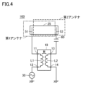
- FIG. 4 is an equivalent circuit diagram of the antenna device 100 according to the first embodiment.
- the antenna device 100 couples the excitation electrode 51 of the slot antenna connected to the power supply circuit 30 and the excitation electrode 52 of the slot antenna that is not fed by the power supply circuit 30 using the antenna coupling element 10.
- the excitation electrode 51 and the opening 25 form a slot antenna (first antenna).
- the excitation electrode 51 is electrically connected to the first external electrode 11 of the antenna coupling element 10
- the power supply circuit 30 is electrically connected to the second external electrode 12 of the antenna coupling element 10.
- the coil L1 of the antenna coupling element 10 is connected in series to the excitation electrode 51 and the power supply circuit 30.
- the excitation electrode 52 and the opening 25 form a slot antenna (second antenna).
- the excitation electrode 52 is electrically connected to the third external electrode 13 of the antenna coupling element 10, and the fourth external electrode 14 of the antenna coupling element 10 is connected (grounded) to GND.
- the antenna coupling element 10 is connected in series to the excitation electrode 52 and GND.
- a capacitance element 60 is provided between the excitation electrode 52 and the third external electrode 13.
- Coil L1 and coil L2 are positioned within antenna coupling element 10 at a position where they are magnetically coupled, generating mutual inductance M.
- antenna coupling element 10 is a chip coil component formed by laminating multiple ceramic green sheets.
- antenna device 100 is not limited to a configuration in which excitation electrodes 51 and 52 are connected to antenna coupling element 10, which is a chip coil component, and may have any configuration as long as coil L1 and coil L2 are positioned at a position where they are magnetically coupled.
- Figure 5 is a diagram showing the frequency characteristics of the reflection coefficient of the antenna device 100 according to the first embodiment.
- the horizontal axis is frequency
- the vertical axis is reflection coefficient (return loss).
- reflection coefficient A is the reflection coefficient when looking at the antenna coupling element 10 side from the power supply circuit 30 in Figure 4 (i.e., of the antenna device 100).
- reflection coefficient A resonance occurs at mark M1 (approximately 2.5 GHz) at the fundamental resonant frequency of antenna device 100. Furthermore, for reflection coefficient A, resonance occurs at mark M2 (approximately 5.4 GHz) and mark M3 (approximately 6.6 GHz) at the harmonic resonant frequencies of antenna device 100.
- antenna device 100 by coupling a slot antenna including excitation electrode 52 to a slot antenna including excitation electrode 51 in antenna coupling element 10, the number of resonant points can be increased, allowing resonance to occur in a wide band including approximately 5.0 GHz to approximately 7.0 GHz.
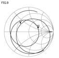
- FIG. 6 is a diagram showing a Smith chart of the antenna device 100 according to the first embodiment.
- the Smith chart shown in FIG. 6 illustrates a case where the impedance of the antenna device 100 is adjusted by providing a capacitive element 60 between the coil L2 and the excitation electrode 52 of the antenna device 100 shown in FIG. 4.
- the antenna device 100 also adjusts the impedance by making the length of the excitation electrode 52 in the X direction shorter than that of the excitation electrode 51, as shown in FIG. 1.
- the target frequency line from 2 GHz to 8 GHz forms large circles near each of the marks M1 (approximately 2.5 GHz), M2 (approximately 5.4 GHz), and M3 (approximately 6.6 GHz). Therefore, from the Smith chart shown in FIG. 6, it can be seen that the antenna device 100 increases the number of resonance points in addition to the fundamental wave resonance frequency (approximately 2.5 GHz), and generates resonance in a wide band including approximately 5.0 GHz to approximately 7.0 GHz.
- FIG 7 is a schematic diagram of the antenna device 200 for comparison. Unlike the antenna device 100, the antenna device 200 does not couple a slot antenna including an excitation electrode 52 to a slot antenna including an excitation electrode 51 using the antenna coupling element 10, but is configured only with a slot antenna including an excitation electrode 51. Note that in the antenna device 200, the same components as those in the antenna device 100 shown in Figure 1 are given the same reference numerals and detailed descriptions will not be repeated.
- an excitation electrode 51 is disposed at a position corresponding to the opening 25.
- the excitation electrode 51 is connected to a power supply circuit 30 (not shown) via wiring on the substrate 40, and is supplied with power from the power supply circuit 30.
- a slot antenna formed by the opening 25 and the excitation electrode 51 functions as a power supply antenna.
- Figure 8 is a diagram showing the frequency characteristics of the reflection coefficient of the antenna device 200 for comparison.
- the horizontal axis is frequency
- the vertical axis is reflection coefficient (return loss).
- reflection coefficient B is the reflection coefficient of the antenna device 200.
- reflection coefficient B resonance occurs at mark M4 (approximately 2.5 GHz) at the fundamental resonant frequency of antenna device 200. Furthermore, for reflection coefficient B, resonance occurs at mark M5 (approximately 5.5 GHz) at the harmonic resonant frequency of antenna device 200. Antenna device 200 only produces resonance near approximately 5.5 GHz, and is unable to produce resonance in a wide band including approximately 5.0 GHz to approximately 7.0 GHz, as does antenna device 100.
- FIG. 9 is a diagram showing the Smith chart of the comparative antenna device 200.
- the target frequency line from 2 GHz to 8 GHz draws a large circle near each of marks M4 (approximately 2.5 GHz) and M5 (approximately 5.5 GHz). Therefore, from the Smith chart shown in FIG. 9, it can be seen that the antenna device 200 generates a resonance at approximately 5.5 GHz in addition to the fundamental resonant frequency (approximately 2.5 GHz).
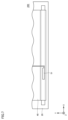
- Fig. 10 is a perspective view of the antenna coupling element 10 according to the first embodiment.
- Fig. 11 is a plan view of the antenna coupling element 10 according to the first embodiment.
- the short side direction of the antenna coupling element 10 is the X direction
- the long side direction is the Y direction
- the height direction is the Z direction.
- the layering direction of the substrate is the Z direction
- the direction of the arrow indicates the upward layer direction.
- the antenna coupling element 10 is a rectangular parallelepiped chip component that couples the resonances of two excitation electrodes 51, 52 in a slot antenna.
- a first external electrode 11, a second external electrode 12, a third external electrode 13, and a fourth external electrode 14 are formed on the outer surface of the antenna coupling element 10 as shown in FIG. 1.
- the antenna coupling element 10 also has a pair of mutually opposing main surfaces, with the lower main surface in FIG. 1 being the mounting surface that faces the circuit board.
- the antenna coupling element 10 contains two coils L1 and L2 to magnetically couple the resonances of the two excitation electrodes 51 and 52 in the slot antenna, and coils L1 and L2 form a transformer that magnetically couples.
- the antenna coupling element 10 is composed of an insulator 1 (ceramic element) made of ceramic layers in which multiple substrates (ceramic green sheets) on which coil wiring is formed are stacked.
- the insulator 1 has a pair of opposing main surfaces and a side surface connecting the main surfaces.
- a plurality of first conductor patterns 21, a second conductor pattern 22, a plurality of third conductor patterns 23, and a fourth conductor pattern 24 are stacked in parallel to the main surface of the insulator 1 to form the antenna coupling element 10 containing the coils L1 and L2.
- the coil L1 has two layers of first conductor patterns 21a, 21b and one layer of second conductor pattern 22 stacked on top of each other, with each conductor pattern electrically connected by via conductors 31. Specifically, the coil L1 connects the two layers of first conductor patterns 21, the first conductor pattern 21a and the first conductor pattern 21b, in parallel by via conductors 31, and connects the second conductor pattern 22 in series to the first conductor pattern 21 of the second layer by via conductors 31. Therefore, the coil L1 can reduce the inductance component compared to when the first conductor pattern 21a and the second conductor pattern 22 are connected in series.
- the first conductor pattern 21 may be a conductor pattern of two or more layers.
- the coil L2 has two layers of third conductor patterns 23a, 23b and one layer of fourth conductor pattern 24 stacked on top of each other, with each conductor pattern being electrically connected by via conductors 32. Specifically, the coil L2 connects the two layers of third conductor patterns 23a and 23a in parallel by via conductors 32, and connects the fourth conductor pattern 24 in series to the third conductor pattern 23 in the second layer by via conductors 32. Therefore, the coil L2 can reduce the inductance component compared to when the third conductor pattern 23a and the fourth conductor pattern 24 are connected in series.
- the third conductor pattern 23 may be a conductor pattern of two or more layers.
- the coil L1 and the coil L2 are arranged in the insulator 1 so that the opening of the coil L1 at least partially overlaps with the opening of the coil L2 when viewed from the stacking direction of the insulator 1.
- the opening of the coil L1 and the opening of the coil L2 are arranged in a direction shifted from the center of the antenna coupling element 10 in the long side direction and approach the second external electrode 12 provided on the short side of the antenna coupling element 10 when viewed from the stacking direction of the insulator 1.
- the arrangement of the coil L1 and the coil L2 shown in FIG. 11 is one example, and other arrangements may be used.
- the coil L1 and the coil L2 are arranged in the insulator 1 so that the second conductor pattern 22 and the fourth conductor pattern 24 face each other.
- the coil L1 and the coil L2 are configured so that the second conductor pattern 22 of one layer and the fourth conductor pattern 24 of one layer face each other with an insulating layer sandwiched between them, so that the capacitance component is smaller than that of a configuration in which the conductor patterns of three layers face each other with an insulating layer sandwiched between them.
- the coupling coefficient between coil L1 and coil L2 can be maintained high compared to when coil L1 and coil L2 are arranged so that the first conductor pattern 21 of the second layer and the third conductor pattern 23 of the second layer face each other. Therefore, by arranging coil L1 and coil L2 so that the second conductor pattern 22 and the fourth conductor pattern 24 face each other, the mutual inductance M between coil L1 and coil L2 does not decrease in the antenna coupling element 10.
- a first external electrode 11 is provided on one short side of the side of the insulator 1
- a second external electrode 12 is provided on the other short side
- a third external electrode 13 is provided on one long side
- a fourth external electrode 14 is provided on the other long side.
- Each of the multiple first conductor patterns 21 is electrically connected to the first external electrode 11. Of the multiple first conductor patterns 21, only the lower first conductor pattern 21b may be electrically connected to the first external electrode 11, and the upper first conductor pattern 21a may be electrically connected to the first conductor pattern 21b through a via conductor.
- the second conductor pattern 22 is electrically connected to the second external electrode 12.
- Each of the multiple third conductor patterns 23 is electrically connected to the third external electrode 13. Of the multiple third conductor patterns 23, only the lower third conductor pattern 23b may be electrically connected to the third external electrode 13, and the upper third conductor pattern 23a may be electrically connected to the third conductor pattern 23b via a via conductor.
- the fourth conductor pattern 24 is electrically connected to the fourth external electrode 14.
- Fig. 12 is a first exploded plan view showing the configuration of the antenna coupling element 10 according to the first embodiment.
- Fig. 13 is a second exploded plan view showing the configuration of the antenna coupling element 10 according to the first embodiment.
- the first conductor pattern 21 to the fourth conductor pattern 24 are each formed by printing a conductive paste (Ni paste) by screen printing on ceramic green sheets 1a to 1o, which are substrates.
- conductor patterns 11a to 14a are formed on ceramic green sheet 1a at positions corresponding to first external electrode 11 to fourth external electrode 14.
- a direction identification mark DDM is provided on ceramic green sheet 1a to indicate that it is the top surface, which is the surface opposite to the mounting surface. This direction identification mark DDM is used to detect the direction of a chip component, for example, when mounting the antenna coupling element 10 on a circuit board using a mounting machine.
- No conductor patterns are formed on ceramic green sheets 1b to 1e, as shown in FIG. 12(b) to 12(e).
- a third conductor pattern 23a is formed on the ceramic green sheet 1f as shown in FIG. 12(f).
- the third conductor pattern 23a is formed clockwise from the center of the upper long side of the ceramic green sheet 1f in the figure, covering approximately 1/2 to 3/4 of the circumference.
- the starting end of the third conductor pattern 23a is formed to the outer periphery of the ceramic green sheet 1f so that it can be electrically connected to the third external electrode 13.
- a connection portion 32a that connects to the via conductor 32 is provided at the end of the third conductor pattern 23a.
- a third conductor pattern 23b is formed on the ceramic green sheet 1g as shown in FIG. 12(g).
- the third conductor pattern 23b is formed clockwise from the center of the upper long side of the ceramic green sheet 1g in the figure, covering approximately 1/2 to 3/4 of the circumference.
- the starting end of the third conductor pattern 23b is formed to the outer periphery of the ceramic green sheet 1g so that it can be electrically connected to the third external electrode 13.
- a connection portion 32b that connects to the via conductor 32 is provided at the end of the third conductor pattern 23b.
- a fourth conductor pattern 24 is formed on the ceramic green sheet 1h as shown in FIG. 12(h).
- the fourth conductor pattern 24 is formed from the center of the lower long side of the ceramic green sheet 1h in the figure, going counterclockwise for about 1/2 to 3/4 of the way around.
- the starting end of the fourth conductor pattern 24 is formed all the way to the outer periphery of the ceramic green sheet 1h so that it can be electrically connected to the fourth external electrode 14. Meanwhile, a connection portion 32c that connects to the via conductor 32 is provided at the end of the fourth conductor pattern 24.
- the antenna coupling element 10 can adjust the degree of coupling between the coil L1 and the coil L2 by adjusting the interlayer distance between the fourth conductor pattern 24 and the second conductor pattern 22.
- the second conductor pattern 22 is formed on the ceramic green sheet 1j as shown in FIG. 13(j).
- the second conductor pattern 22 is formed so as to go counterclockwise around about 1/2 of the way from the center of the short side on the left side of the ceramic green sheet 1j in the figure.
- the starting end of the second conductor pattern 22 is formed to the outer periphery of the ceramic green sheet 1j so as to be electrically connected to the second external electrode 12. Meanwhile, the end of the second conductor pattern 22 is provided with a connection portion 31a that connects to the via conductor 31.
- the first conductor pattern 21a is formed on the ceramic green sheet 1k as shown in FIG. 13(k).
- the first conductor pattern 21a is formed so as to go around about 3/4 to one revolution clockwise from the center of the short side on the right side of the ceramic green sheet 1k in the figure.
- the starting end of the first conductor pattern 21a is formed to the outer periphery of the ceramic green sheet 1k so that it can be electrically connected to the first external electrode 11. Meanwhile, the end of the first conductor pattern 21a is provided with a connection portion 31b that connects to the via conductor 31.
- the ceramic green sheet 1l only has a connection portion 31c that connects to the via conductor 31, and no conductor pattern is formed.
- the interlayer distance between the first conductor pattern 21a and the first conductor pattern 21b is longer than the interlayer distance between the third conductor pattern 23a and the third conductor pattern 23b, or the interlayer distance between the first conductor pattern 21b and the second conductor pattern 22.
- the first conductor pattern 21b is the first conductor pattern that faces the second conductor pattern 22 among the multiple first conductor patterns 21. In this way, the antenna coupling element 10 can adjust the inductance component of the coil L1 by adjusting the interlayer distance between the first conductor pattern 21a and the first conductor pattern 21b.
- the first conductor pattern 21b is formed on the ceramic green sheet 1m as shown in FIG. 13(m).
- the first conductor pattern 21b is formed so as to go around about 3/4 to one revolution clockwise from the center of the short side on the right side of the ceramic green sheet 1m in the figure.
- the starting end of the first conductor pattern 21b is formed to the outer periphery of the ceramic green sheet 1m so as to be electrically connected to the first external electrode 11. Meanwhile, the end of the first conductor pattern 21b is provided with a connection portion 31d that connects to the via conductor 31.
- the substrate constituting the insulator 1 has been described as a ceramic green sheet, it may be a non-magnetic ceramic insulator made of LTCC (Low Temperature Co-fired Ceramics) or a resin insulator made of a resin material such as polyimide or liquid crystal polymer.
- the antenna coupling element 10 functions as an antenna coupling element even in high frequency bands exceeding several hundred MHz by using a non-magnetic material for the substrate constituting the insulator 1 (as it is not magnetic ferrite).
- each conductor pattern and via conductor are made of a conductor material with low resistivity, mainly composed of Ag or Cu.
- the substrate constituting the insulator 1 is ceramic, they are formed, for example, by screen printing and firing a conductive paste mainly composed of Ag or Cu.
- the substrate constituting the insulator 1 is resin, they are formed, for example, by patterning a metal foil such as an Al foil or a Cu foil by etching or the like.
- the antenna coupling element 10 shown in Figs. 10 to 13 is an example, and the antenna coupling element 10 is not limited to this configuration as long as it contains at least two coils L1 and L2 and constitutes a transformer in which the coils L1 and L2 are magnetically coupled.
- the antenna coupling element 10 may include a conductor pattern that is not electrically connected to the first external electrode 11 or the second external electrode 12 among the multiple conductor patterns constituting the coil L1, and may include a conductor pattern that is not electrically connected to the third external electrode 13 or the fourth external electrode 14 among the multiple conductor patterns constituting the coil L2.
- the slot antenna including the excitation electrode 52 in the antenna coupling element 10 is coupled to the slot antenna including the excitation electrode 51. That is, in the antenna device 100, the resonance of the two excitation electrodes 51 and 52 in the slot antenna is magnetically coupled via the coils L1 and L2 constituting a transformer. Specifically, since the power supply circuit 30 is connected to the second external electrode 12 of the antenna coupling element 10 and the excitation electrode 51 is connected to the first external electrode 11, when power is supplied from the power supply circuit 30 to the excitation electrode 51, a current I1 flows through the first conductor patterns 21a and 21b and the second conductor pattern 22.
- the current I1 flows through the second conductor pattern 22 in a direction toward the connection portion 31a as shown by the arrow in FIG. 13(j) and flows through the first conductor patterns 21a and 21b in a direction away from the connection portions 31b and 31d as shown by the arrows in FIG. 13(k) and (m).
- Current I2 flows through coil L2, which generates a magnetic field in the opposite direction so that coil L2, which constitutes a transformer, cancels out the magnetic field generated in coil L1 by current I1.
- current I2 flows through third conductor patterns 23a and 23b in the direction toward connection portions 32a and 32b as shown by the arrows in Figures 12(f) and 12(g), and flows through fourth conductor pattern 24 in the direction away from connection portion 32c as shown by the arrow in Figure 12(h).
- FIG. 14 is a schematic diagram of another comparative antenna device 201.
- Antenna device 201 does not connect excitation electrode 51 and excitation electrode 52 to antenna coupling element 10 as in antenna device 100, but has a configuration in which excitation electrodes 51 and 52 are connected in parallel to substrate 40. Note that in antenna device 201, the same components as those in antenna device 100 shown in FIG. 1 are designated by the same reference numerals and detailed description will not be repeated.
- excitation electrodes 51 and 52 are disposed at a position corresponding to the opening 25.
- the excitation electrode 51 is not connected to the antenna coupling element 10, but is connected to the power supply circuit 30 (not shown) via wiring on the substrate 40, and is supplied with power from the power supply circuit 30.
- the excitation electrode 52 is not connected to the antenna coupling element 10, but is connected to the substrate 40 and is connected to GND (earthed).
- the slot antenna formed by the opening 25 and the excitation electrode 51 functions as a power supply antenna
- the slot antenna formed by the opening 25 and the excitation electrode 52 functions as a non-powered antenna, but the excitation electrodes 51 and 52 are only electric field coupled, and are not magnetic field coupled.
- Figure 15 is a diagram showing the frequency characteristics of the reflection coefficient of another comparative antenna device 201.
- the horizontal axis is frequency
- the vertical axis is reflection coefficient (return loss).
- reflection coefficient C is the reflection coefficient of the antenna device 201.
- reflection coefficient C resonance occurs at mark M6 (approximately 2.6 GHz) at the fundamental resonant frequency of antenna device 201. Furthermore, for reflection coefficient C, resonance occurs at mark M7 (approximately 5.6 GHz) at the harmonic resonant frequency of antenna device 201. Antenna device 201 only causes resonance near approximately 5.6 GHz, does not add any resonant points like antenna device 100, and is unable to cause resonance in a wide band including approximately 5.0 GHz to approximately 7.0 GHz.
- FIG. 16 is a diagram showing the Smith chart of another comparative antenna device 201.
- the target frequency line from 2 GHz to 8 GHz draws a large circle near each of marks M6 (approximately 2.6 GHz) and M7 (approximately 5.6 GHz). Therefore, it can be seen from the Smith chart shown in FIG. 16 that the antenna device 201 only produces resonance at approximately 5.6 GHz in addition to the fundamental resonant frequency (approximately 2.6 GHz).
- FIG. 17 is a schematic diagram of yet another comparative antenna device 202. Unlike antenna device 100, antenna device 202 does not connect excitation electrodes 51 and 52 to antenna coupling element 10, but connects excitation electrodes 51 and 52 to substrate 40 by crossing their connection parts. Note that in antenna device 202, the same components as those in antenna device 100 shown in FIG. 1 are designated by the same reference numerals and detailed descriptions will not be repeated.
- excitation electrodes 51 and 52 are disposed at a position corresponding to the opening 25.
- the excitation electrode 51 is not connected to the antenna coupling element 10, but is connected to the power supply circuit 30 (not shown) via wiring on the substrate 40, and is supplied with power from the power supply circuit 30.
- the excitation electrode 52 is not connected to the antenna coupling element 10, but is connected to the substrate 40 across the connection portion of the excitation electrode 51, and is connected (grounded) to GND.
- the slot antenna formed by the opening 25 and the excitation electrode 51 functions as a powered antenna
- the slot antenna formed by the opening 25 and the excitation electrode 52 functions as a non-powered antenna, but the connection portions of the excitation electrodes 51 and 52 cross, and the excitation electrodes 51 and 52 are only electric field coupled, but are not magnetic field coupled.
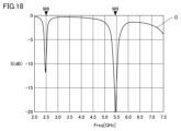
- Figure 18 is a diagram showing the frequency characteristics of the reflection coefficient of yet another comparative antenna device 202.
- the horizontal axis is frequency
- the vertical axis is reflection coefficient (return loss).
- reflection coefficient D is the reflection coefficient of the antenna device 202.
- reflection coefficient D resonance occurs at mark M8 (approximately 2.5 GHz) at the fundamental resonant frequency of antenna device 202. Furthermore, for reflection coefficient D, resonance occurs at mark M9 (approximately 5.5 GHz) at the harmonic resonant frequency of antenna device 202. Antenna device 202 only generates resonance near approximately 5.5 GHz, does not add any resonant points like antenna device 100, and is unable to generate resonance in a wide band including approximately 5.0 GHz to approximately 7.0 GHz.
- FIG. 19 is a diagram showing the Smith chart of yet another comparative antenna device 202.
- the target frequency line from 2 GHz to 8 GHz draws large circles near both mark M8 (approximately 2.5 GHz) and mark M9 (approximately 5.5 GHz). Therefore, from the Smith chart shown in FIG. 19, it can be seen that the antenna device 202 only produces resonance at approximately 5.5 GHz in addition to the fundamental resonant frequency (approximately 2.5 GHz).
- antenna device 100 it is clear that the effect of coupling a slot antenna including excitation electrode 52 to a slot antenna including excitation electrode 51 in antenna coupling element 10 is to increase the number of resonance points and cause resonance over a wide band.
- the antenna device 100 can change the frequency characteristics near the added resonance point and change the width of the band in which resonance occurs by adjusting the impedance of the slot antenna including the excitation electrode 52 coupled to the slot antenna including the excitation electrode 51 by the antenna coupling element 10.
- Possible methods for adjusting the impedance of the slot antenna including the excitation electrode 52 include, for example, changing the length of the excitation electrode 52 in the X direction, or changing the capacitance value of the capacitance element 60 connected between the coil L2 and the excitation electrode 52.
- the length in the X direction of the excitation electrode 52 is approximately half the length in the X direction of the excitation electrode 51, and the capacitance value of the capacitance element 60 is set to 0.3 pF to adjust the impedance.
- This section explains how adjusting the impedance in this way changes the frequency characteristics near the added resonance point. Specifically, this section explains the characteristics of the antenna device 100 in which the impedance is adjusted to a capacitance value of 0 (zero) F.
- Figure 20 is a diagram showing the frequency characteristics of the reflection coefficient of the antenna device 100 in which the capacitance value of the capacitive element is changed.
- the horizontal axis is frequency and the vertical axis is reflection coefficient (return loss).
- the reflection coefficient E is the reflection coefficient of the antenna device 100 in which the capacitance value of the capacitive element 60 is changed to 0 (zero) F.
- reflection coefficient E resonance occurs at mark M11 (approximately 2.5 GHz) at the fundamental resonance frequency of the antenna device 100. Furthermore, for reflection coefficient E, resonance occurs at mark M12 (approximately 5.2 GHz) and mark M13 (approximately 6.5 GHz) at the harmonic resonance frequency of the antenna device 100. Therefore, even in the antenna device 100 in which the capacitance value of the capacitance element 60 is changed to 0 (zero) F, it is possible to increase the number of resonance points.
- reflection coefficient E only causes resonance near mark M12 (approximately 5.2 GHz) and mark M13 (approximately 6.5 GHz), and is unable to cause resonance in a wide band including approximately 5.0 GHz to approximately 7.0 GHz, as with reflection coefficient A shown in FIG. 5.
- FIG. 21 is a diagram showing the Smith chart of the antenna device 100 in which the capacitance value of the capacitance element is changed.
- the target frequency line from 2 GHz to 8 GHz draws circles near each of the marks M11 (about 2.5 GHz), M12 (about 5.2 GHz), and M13 (about 6.5 GHz).
- the circles drawn near each of the marks M12 (about 5.2 GHz) and M13 (about 6.5 GHz) are smaller than the large circles drawn near each of the marks M2 and M3 in the Smith chart shown in FIG. 6. Therefore, from the Smith chart shown in FIG.
- the antenna device 100 in which the capacitance value of the capacitance element 60 is changed to 0 (zero) F is able to increase the number of resonance points, but does not cause resonance in a wide band including about 5.0 GHz to about 7.0 GHz.
- the excitation electrodes 51, 52 are formed on the substrate 40 disposed on the conductor 20, and are therefore disposed at a position different from the opening 25 in the Z direction.
- the excitation electrodes 51, 52 may be disposed at a position overlapping with the opening 25 in the Z direction.
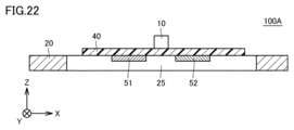
- FIG. 22 is a cross-sectional view of an antenna device 100A according to a modified example.
- the same components as those of the antenna device 100 shown in FIGS. 1 to 3 are denoted by the same reference numerals and detailed description will not be repeated.
- the excitation electrodes 51 and 52 are formed on the surface of the substrate 40 opposite to the surface of the substrate 40 that contacts the conductor 20.
- the excitation electrodes 51 and 52 are formed on the surface of the substrate 40 that contacts the conductor 20.
- the excitation electrodes 51 and 52 are arranged at positions where the opening 25 and the excitation electrodes 51 and 52 overlap in the Z direction.
- the antenna coupling element 10 is arranged at a position where it does not overlap the conductor 20 in the Z direction, but the antenna coupling element 10 may also be arranged at a position where it overlaps in the Z direction with the same opening 25 as the excitation electrodes 51 and 52, or the excitation electrodes 51 and 52 may be arranged on different surfaces of the substrate 40.
- an opening 25 (slot) long in the X direction is provided in the plate-like conductor 20, and excitation electrodes 51, 52 are arranged at positions corresponding to the opening 25.
- the excitation electrodes 51, 52 are provided along the long side 25a of the opening 25, and are excited as an antenna by electric field coupling (capacitive coupling) between the excitation electrodes 51, 52 and the peripheral portion of the opening 25.
- an antenna excited by electric field coupling between the excitation electrode and the peripheral portion of the opening is combined with an antenna excited by passing a current through the peripheral portion of the opening.
- FIG. 23 is a schematic diagram of an electronic device including an antenna device 100B according to embodiment 2.
- the electronic device includes the antenna device 100B, a power supply circuit 30 that supplies power to an excitation electrode 51a (first excitation electrode), and a housing 300 that houses the antenna device 100B and the power supply circuit 30.
- the same components as those in the electronic device including the antenna device 100 shown in FIG. 1 are designated by the same reference numerals and detailed descriptions will not be repeated.
- the antenna device 100B has an opening 25 (slot) that is long in the X direction provided in the plate-shaped conductor 20, and an excitation electrode 51a (also called an excitation conductor, feed line, or simply a microstrip line) is disposed near the opening 25.
- the antenna device 100B is excited as a slot antenna by operating the excitation electrode 51a as a capacitive feeding element for the opening 25, and electric field coupling (capacitive coupling) between the excitation electrode 51a and the periphery of the opening 25.
- the excitation electrode 51a is also electrically connected to one end (first external electrode 11) of the coil L1 of the antenna coupling element 10 mounted on the substrate 40. As shown in FIG. 23, the excitation electrode 51a is connected to the power supply circuit 30 via the antenna coupling element 10, and power is supplied from the power supply circuit 30. In other words, the slot antenna formed by the opening 25 and the excitation electrode 51a functions as a power supply antenna.
- the other end (second external electrode 12) of the coil L1 of the antenna coupling element 10 is electrically connected to the power supply circuit 30.
- the antenna device 100B does not have an excitation electrode 52, and one end (fourth external electrode 14) of the coil L2 of the antenna coupling element 10 is connected to the GND electrode 41 (substrate electrode) of the substrate 40.
- the antenna device 100B is excited by current flowing from the power supply circuit 30 to the periphery of the opening 25 via the coil L1 that is magnetically coupled to the coil L2.
- the antenna device 100B has the resonant frequency of the slot antenna excited by the excitation electrode 51a, as well as the resonant frequency of the antenna excited by the connection between the antenna coupling element 10 and the GND electrode 41, making it possible to widen the usable frequency band.
- the other end of the coil L2 (third external electrode 13) may or may not be connected to the substrate 40, but is not electrically connected to an electrode such as a GND electrode. Connecting the other end of the coil L2 to the substrate 40 improves the mounting strength of the antenna coupling element 10 relative to the substrate 40.
- the GND electrode 41 shown in FIG. 23 is strip-shaped and arranged in the X direction of the substrate 40 parallel to the opening 25, but is not limited to this shape and may have any shape that allows connection of one end of the power supply circuit 30 and one end of the coil L2.
- the GND electrode 41 may also be divided into a portion that electrically connects to one end of the power supply circuit 30 and a portion that electrically connects to one end of the coil L2, and both portions may be electrically connected to the conductor 20 arranged on the housing 300.
- one end of the coil L2 is connected to the GND electrode 41, and the current of the power supply circuit 30 is passed through the magnetically coupled coil L1 to the periphery of the opening 25, exciting the antenna. Therefore, the current flowing through the periphery of the opening 25 changes depending on the relationship between the position where one end of the power supply circuit 30 is electrically connected to the GND electrode 41 and the position where one end of the coil L2 is electrically connected to the GND electrode 41, and the resonant frequency of the antenna excited by that current also changes.
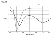
- FIG. 24 is a diagram showing the frequency characteristics of the reflection coefficient of the antenna device 100B according to the second embodiment.
- FIG. 25 is a diagram showing the antenna efficiency of the antenna device 100B according to the second embodiment.
- the horizontal axis is frequency
- the vertical axis is reflection coefficient (return loss).
- the horizontal axis is frequency
- the vertical axis is antenna efficiency.
- Reflection coefficient F shown in FIG. 24 indicates the reflection coefficient of antenna device 100B
- reflection coefficient G indicates the reflection coefficient of a slot antenna without an antenna coupling element.
- resonance coefficient G resonance occurs at approximately 2.3 GHz, the resonant frequency of the slot antenna excited by excitation electrode 51a.
- reflection coefficient F resonance occurs at approximately 3.0 GHz, the resonant frequency of the antenna excited by connecting antenna coupling element 10 to GND electrode 41. Therefore, antenna efficiency H of antenna device 100B shown in FIG. 25 maintains high efficiency from approximately 2.3 GHz to approximately 3.0 GHz.
- the antenna device 100B can increase the number of resonance points and generate resonance in a wide band including approximately 2.3 GHz to approximately 3.0 GHz by adding an antenna excited by the connection between the antenna coupling element 10 and the GND electrode 41 in addition to the slot antenna excited by the excitation electrode 51a. Furthermore, the antenna device 100B can achieve good antenna efficiency in a wide band.
- Modification 1 23 , the position where one end of the power supply circuit 30 is electrically connected to the GND electrode 41 and the position where one end of the coil L2 is electrically connected to the GND electrode 41 are on the same side of the opening 25.
- an antenna device in which the position where one end of the power supply circuit is electrically connected to the GND electrode and the position where one end of the coil L2 is electrically connected to the GND electrode are on different sides of the opening 25 will be described.
- FIG. 26 is a schematic diagram of an electronic device including an antenna device 100C according to Variation 1 of Embodiment 2.
- the electronic device includes the antenna device 100C, a power supply circuit 30 that supplies power to the excitation electrode 51a (excitation electrode), and a housing 300 that houses the antenna device 100C and the power supply circuit 30.
- the same components as those in the electronic device including the antenna device 100 shown in FIG. 1 and the antenna device 100B shown in FIG. 23 are designated by the same reference numerals and detailed descriptions will not be repeated.
- the antenna device 100C has an opening 25 that is long in the X direction provided in the plate-shaped conductor 20, and an excitation electrode 51a is disposed near the opening 25.
- the antenna device 100C is excited as a slot antenna by the excitation electrode 51a acting as a capacitive feeding element for the opening 25 and the excitation electrode 51a and the periphery of the opening 25 being electric field coupled (capacitively coupled).
- the slot antenna formed by the opening 25 and the excitation electrode 51a functions as a feeding antenna.
- one end (fourth external electrode 14) of the coil L2 is connected to the GND electrode 42 (substrate electrode) of the substrate 40.
- the antenna device 10C is excited by current flowing from the power supply circuit 30 to the periphery of the opening 25 via the coil L1, which is magnetically coupled with the coil L2.
- the GND electrode 42 shown in FIG. 26 is L-shaped, including a portion that is provided in the X direction of the substrate 40 parallel to the opening 25, and a portion that is provided in the Y direction of the substrate 40 and overlaps with the opening 25. Since the opening 25 and a portion of the GND electrode 42 overlap when viewed from the Z direction, the opening of the slot antenna is the portion of the opening 25 excluding the portion where the GND electrode 42 overlaps. Note that, although FIG. 26 describes a configuration in which the opening 25 and a portion of the GND electrode 42 overlap when viewed from the Z direction, the GND electrode 42 may be L-shaped so as not to overlap the opening 25 when viewed from the Z direction.
- the position where one end of the power supply circuit 30 is electrically connected to the GND electrode 42 and the position where one end of the coil L2 is electrically connected to the GND electrode 42 are provided on different sides of the opening 25. Specifically, one end of the power supply circuit 30 is provided on the X-direction side of the GND electrode 42, and one end of the coil L2 is provided on the Y-direction side of the GND electrode 42. Therefore, in the antenna device 100C, the position where one end of the coil L2 is electrically connected to the GND electrode 42 is moved away from the position where one end of the power supply circuit 30 is electrically connected to the GND electrode 42, thereby improving the antenna characteristics by preventing the resonances of the two antennas from interfering with each other.
- the GND electrode 42 may be divided into an electrode that is electrically connected to one end of the power supply circuit 30 and an electrode that is electrically connected to one end of the coil L2, and both electrodes may be electrically connected to the conductor 20 and the housing 300 and provided on different sides of the opening 25.
- FIG. 27 is a schematic diagram of an electronic device including an antenna device 100D according to Variation 2 of Embodiment 2.
- the electronic device includes the antenna device 100D, a power supply circuit 30 that supplies power to the excitation electrode 51a (first excitation electrode), and a housing 300 that houses the antenna device 100D and the power supply circuit 30.
- the same components as those in the electronic device including the antenna device 100 shown in FIG. 1 and the antenna device 100B shown in FIG. 23 are designated by the same reference numerals and detailed descriptions will not be repeated.
- the antenna device 100D has an opening 25 that is long in the X direction provided in the plate-shaped conductor 20, and an excitation electrode 51b is disposed at a position corresponding to the opening 25.
- the antenna device 100D is excited as a slot antenna by the excitation electrode 51b acting as a capacitive feeding element for the opening 25 and the excitation electrode 51b and the periphery of the opening 25 being electric field coupled (capacitively coupled).
- the slot antenna formed by the opening 25 and the excitation electrode 51b functions as a feeding antenna.
- Excitation electrode 51b unlike excitation electrode 51a shown in FIG. 23, has a shape that is long in the X direction along opening 25, one end of which is electrically connected to one end of coil L1 (first external electrode 11), and the other end of which is electrically connected to GND electrode 41 of substrate 40.
- one end (fourth external electrode 14) of the coil L2 is electrically connected to the GND electrode 41 of the substrate 40, and the other end (third external electrode 13) of the coil L2 is also electrically connected to the GND electrode 41.
- the antenna device 100D With the coil L2 connected to the GND electrode 41, the antenna device 100D is excited by current flowing from the power supply circuit 30 to the periphery of the opening 25 via the coil L1 that is magnetically coupled to the coil L2.
- the antenna device 100D not only one end of the power supply circuit 30 and one end of the coil L2, but also one end of the coil L1 and the other end of the coil L2 are electrically connected to the GND electrode 41. Therefore, compared to the antenna device 100B shown in FIG. 23, the antenna device 100D has more starting points for flowing current to the GND electrode 41, which increases the number of paths for flowing current from the power supply circuit 30 to the periphery of the opening 25 via the antenna coupling element 10, thereby making it possible to widen the bandwidth.
- the configuration described in the second modification may be combined with the configuration described in the first modification.
- the excitation electrode 51b and the line connecting the excitation electrode 51b and the GND electrode 41 are drawn separately, but in reality the boundary may not be clear.
- [Modification 3] 23 uses the antenna coupling element 10 to configure a slot antenna excited by an excitation electrode 51a fed by a feed circuit 30, and a parasitic slot antenna.
- an antenna device configuring a powered slot antenna and a parasitic slot antenna without using the antenna coupling element 10 will be described.
- FIG. 28 is a schematic diagram of an electronic device including an antenna device 100E according to the third modification of the second embodiment.
- the electronic device includes the antenna device 100E, a power supply circuit 30 that supplies power to the excitation electrode 51a (first excitation electrode), and a housing 300 that houses the antenna device 100E and the power supply circuit 30.
- the same components as those in the electronic device including the antenna device 100 shown in FIG. 1 and the antenna device 100B shown in FIG. 23 are designated by the same reference numerals and detailed descriptions will not be repeated.
- the antenna device 100E has an opening 25 that is long in the X direction provided in the plate-shaped conductor 20, and an excitation electrode 51a is disposed near the opening 25.
- the antenna device 100E is excited as a slot antenna by the excitation electrode 51a acting as a capacitive feeding element for the opening 25 and the excitation electrode 51a and the periphery of the opening 25 being electric field coupled (capacitively coupled).
- the slot antenna formed by the opening 25 and the excitation electrode 51a functions as a feeding antenna.
- an excitation electrode 52a is disposed near the excitation electrode 51a, and one end of the excitation electrode 52a is connected to the GND electrode 41 (substrate electrode) of the substrate 40.
- the excitation electrode 52a is L-shaped including a portion that is arranged parallel to the excitation electrode 51a (Y direction) and a portion that is arranged parallel to the GND electrode 41 (X direction). Since the excitation electrodes 51a and 52a are electromagnetically coupled in the portion where they are arranged in parallel, a current flows in the excitation electrode 52a due to the current flowing from the power supply circuit 30 to the excitation electrode 51a.
- the antenna device 100E is excited by connecting one end of the excitation electrode 52a to the GND electrode 41, and a current from the power supply circuit 30 flows through the periphery of the opening 25 via the portion where the excitation electrodes 51a and 52a are arranged in parallel. This allows the antenna device 100E to be configured with a slot antenna powered by the power supply circuit 30 and an unpowered slot antenna without using an antenna coupling element 10, thereby reducing manufacturing costs.
- the configuration described in Modification 3 may be combined with the configurations described in Modifications 1 and 2.
- a plate-shaped conductor having an opening; a first excitation electrode and a second excitation electrode disposed at positions corresponding to the opening; a first coil, one end of which is electrically connected to the first excitation electrode and the other end of which is connected to a power supply circuit; a second coil, one end of which is electrically connected to the second excitation electrode;
- the antenna device wherein the first coil and the second coil are disposed in a position where they are magnetically coupled.
- the antenna device can add a resonance point to widen the usable frequency band by connecting the first excitation electrode and the second excitation electrode, which are arranged at positions corresponding to the opening, to the first coil and the second coil, which are magnetically coupled, respectively.
- the antenna device (2) The antenna device according to (1), The first excitation electrode and the second excitation electrode are disposed at positions overlapping with the opening when the opening is viewed from above.
- the antenna device according to (2), The device further includes a substrate disposed between the first and second excitation electrodes and the conductor.
- the antenna device is rectangular in shape with a second side shorter than the first side,
- the first excitation electrode and the second excitation electrode are in a band shape extending along the first side.
- a first direction in which the first excitation electrode extends and a second direction in which the second excitation electrode extends are opposite along the first side.
- the antenna device according to any one of (1) to (5), The sensor further includes a capacitive element connected in series between the second coil and the second excitation electrode.
- the antenna coupling element includes a first coil and a second coil, An insulator; a first external electrode, a second external electrode, a third external electrode, and a fourth external electrode formed on a surface of an insulator; a first coil and a second coil each formed of a plurality of conductor patterns within an insulator; The plurality of conductor patterns constituting the first coil are electrically connected to the first external electrode or the second external electrode, the plurality of conductor patterns constituting the second coil are electrically connected to the third external electrode or the fourth external electrode; When viewed from the lamination direction of the insulators, the opening of the first coil at least partially overlaps with the opening of the second coil.
- the antenna device is electrically connected to the first outer electrode of the antenna coupling element; the feeding circuit is electrically connected to the second external electrode of the antenna coupling element; The second excitation electrode is electrically connected to the third outer electrode of the antenna coupling element; The fourth outer electrode of the antenna coupling element is grounded.
- the antenna device is a first conductor pattern having at least two layers, the first conductor pattern being electrically connected to the first external electrode; a second conductor pattern laminated on the first conductor pattern and electrically connected to the second external electrode, The layers of the first conductor pattern are connected in parallel to each other, and the second conductor pattern is connected in series to the first conductor pattern;
- the second coil is a third conductor pattern having at least two layers, the third conductor pattern being electrically connected to the third external electrode; a fourth conductor pattern laminated on the third conductor pattern and electrically connected to the fourth external electrode, the layers of the third conductor pattern are connected in parallel to each other, and the fourth conductor pattern is connected in series to the third conductor pattern;
- the first coil and the second coil are disposed within the insulator such that the second conductor pattern and the fourth conductor pattern face each other in the stacking direction.
- An antenna device according to any one of (1) to (9), a power supply circuit for supplying power to the first excitation electrode;
- An electronic device comprising: a housing that houses an antenna device and a power supply circuit.
- a plate-shaped conductor having an opening; An excitation electrode disposed at a position corresponding to the opening; a first coil, one end of which is electrically connected to the excitation electrode and the other end of which is connected to a power supply circuit; a second coil having one end electrically connected to a substrate electrode electrically connected to the conductor; The first coil and the second coil are disposed in a position where they are magnetically coupled to each other.
- the antenna device can add a resonance point to widen the usable frequency band by magnetically coupling a first coil, one end of which is electrically connected to an excitation electrode and the other end of which is connected to a power supply circuit, and a second coil, one end of which is electrically connected to a board electrode that is electrically connected to a conductor.
- the antenna device according to any one of (11) and (12),
- the substrate electrode is provided along at least two sides of the opening, a power supply circuit is electrically connected to a portion of the substrate electrode provided along the first side of the opening;
- One end of the second coil is electrically connected to a portion of the board electrode that is provided along a second side of the opening that is different from the first side.
- the antenna device includes a first coil and a second coil, An insulator; a first external electrode, a second external electrode, a third external electrode, and a fourth external electrode formed on a surface of an insulator; a first coil and a second coil each formed of a plurality of conductor patterns within an insulator; The plurality of conductor patterns constituting the first coil are electrically connected to the first external electrode or the second external electrode, the plurality of conductor patterns constituting the second coil are electrically connected to the third external electrode or the fourth external electrode; When viewed from the lamination direction of the insulators, the opening of the first coil at least partially overlaps with the opening of the second coil.
- the antenna device according to (14), a power supply circuit for supplying power to the excitation electrodes; and a housing that houses the antenna device and the power supply circuit.
- 10 antenna coupling element 11 first external electrode, 12 second external electrode, 13 third external electrode, 14 fourth external electrode, 20 conductor, 21, 21a, 21b first conductor pattern, 22, 22A second conductor pattern, 23, 23a, 23b third conductor pattern, 24, 24A fourth conductor pattern, 25 opening, 31, 32 via conductor, 30 power supply circuit, 40 substrate, 51, 52 excitation electrode, 60 capacitance element, 100, 100A, 200, 201, 202 antenna device, 300 housing.
Landscapes
- Engineering & Computer Science (AREA)
- Power Engineering (AREA)
- Microelectronics & Electronic Packaging (AREA)
- Details Of Aerials (AREA)
Priority Applications (3)
| Application Number | Priority Date | Filing Date | Title |
|---|---|---|---|
| JP2024562989A JP7732606B2 (ja) | 2022-12-09 | 2023-12-07 | アンテナ装置、および電子機器 |
| CN202380082708.3A CN120303828A (zh) | 2022-12-09 | 2023-12-07 | 天线装置和电子设备 |
| US19/175,238 US20250239780A1 (en) | 2022-12-09 | 2025-04-10 | Antenna device and electronic apparatus |
Applications Claiming Priority (4)
| Application Number | Priority Date | Filing Date | Title |
|---|---|---|---|
| JP2022196958 | 2022-12-09 | ||
| JP2022-196958 | 2022-12-09 | ||
| JP2023-088797 | 2023-05-30 | ||
| JP2023088797 | 2023-05-30 |
Related Child Applications (1)
| Application Number | Title | Priority Date | Filing Date |
|---|---|---|---|
| US19/175,238 Continuation US20250239780A1 (en) | 2022-12-09 | 2025-04-10 | Antenna device and electronic apparatus |
Publications (1)
| Publication Number | Publication Date |
|---|---|
| WO2024122607A1 true WO2024122607A1 (ja) | 2024-06-13 |
Family
ID=91379068
Family Applications (1)
| Application Number | Title | Priority Date | Filing Date |
|---|---|---|---|
| PCT/JP2023/043793 Ceased WO2024122607A1 (ja) | 2022-12-09 | 2023-12-07 | アンテナ装置、および電子機器 |
Country Status (4)
| Country | Link |
|---|---|
| US (1) | US20250239780A1 (https=) |
| JP (1) | JP7732606B2 (https=) |
| CN (1) | CN120303828A (https=) |
| WO (1) | WO2024122607A1 (https=) |
Cited By (1)
| Publication number | Priority date | Publication date | Assignee | Title |
|---|---|---|---|---|
| WO2026033974A1 (ja) * | 2024-08-08 | 2026-02-12 | 株式会社村田製作所 | アンテナ装置、および電子機器 |
Citations (3)
| Publication number | Priority date | Publication date | Assignee | Title |
|---|---|---|---|---|
| JP2018515005A (ja) * | 2015-03-31 | 2018-06-07 | ビーワイディー カンパニー リミテッドByd Company Limited | アンテナ及びそれを有する移動端末 |
| JP2019535188A (ja) * | 2016-09-29 | 2019-12-05 | 華為技術有限公司Huawei Technologies Co.,Ltd. | 端末 |
| WO2022004114A1 (ja) * | 2020-07-03 | 2022-01-06 | 株式会社村田製作所 | アンテナ装置及び電子機器 |
-
2023
- 2023-12-07 JP JP2024562989A patent/JP7732606B2/ja active Active
- 2023-12-07 WO PCT/JP2023/043793 patent/WO2024122607A1/ja not_active Ceased
- 2023-12-07 CN CN202380082708.3A patent/CN120303828A/zh active Pending
-
2025
- 2025-04-10 US US19/175,238 patent/US20250239780A1/en active Pending
Patent Citations (3)
| Publication number | Priority date | Publication date | Assignee | Title |
|---|---|---|---|---|
| JP2018515005A (ja) * | 2015-03-31 | 2018-06-07 | ビーワイディー カンパニー リミテッドByd Company Limited | アンテナ及びそれを有する移動端末 |
| JP2019535188A (ja) * | 2016-09-29 | 2019-12-05 | 華為技術有限公司Huawei Technologies Co.,Ltd. | 端末 |
| WO2022004114A1 (ja) * | 2020-07-03 | 2022-01-06 | 株式会社村田製作所 | アンテナ装置及び電子機器 |
Cited By (1)
| Publication number | Priority date | Publication date | Assignee | Title |
|---|---|---|---|---|
| WO2026033974A1 (ja) * | 2024-08-08 | 2026-02-12 | 株式会社村田製作所 | アンテナ装置、および電子機器 |
Also Published As
| Publication number | Publication date |
|---|---|
| US20250239780A1 (en) | 2025-07-24 |
| CN120303828A (zh) | 2025-07-11 |
| JP7732606B2 (ja) | 2025-09-02 |
| JPWO2024122607A1 (https=) | 2024-06-13 |
Similar Documents
| Publication | Publication Date | Title |
|---|---|---|
| TWI545841B (zh) | Antenna devices and wireless communication devices | |
| US10211541B2 (en) | Antenna device | |
| US9225057B2 (en) | Antenna apparatus and wireless communication device using same | |
| JP2002319811A (ja) | 複共振アンテナ | |
| JP2013070365A (ja) | 無線通信装置 | |
| CN104871367A (zh) | 多频带用天线 | |
| JP2020014232A (ja) | アンテナ装置および通信端末装置 | |
| CN211088515U (zh) | 天线耦合元件、天线装置及电子设备 | |
| JP6760545B2 (ja) | アンテナ結合素子、アンテナ装置及び通信端末装置 | |
| JP2014165683A (ja) | アンテナ及び電子装置 | |
| JPWO2010013610A1 (ja) | 平面アンテナ | |
| US20240235516A1 (en) | Filter device, antenna device, and antenna module | |
| JP7732606B2 (ja) | アンテナ装置、および電子機器 | |
| US12586704B2 (en) | Coil element, antenna device, and electronic device | |
| WO2014104228A1 (ja) | マルチバンドアンテナ及び無線装置 | |
| WO2023032510A1 (ja) | コイル素子、アンテナ装置、および電子機器 | |
| US20180351240A1 (en) | Antenna device and electronic apparatus | |
| WO2023032511A1 (ja) | アンテナ装置、および通信端末装置 | |
| JP5408187B2 (ja) | アンテナ装置及びこれを用いた無線通信機器 | |
| US20260039268A1 (en) | Filter device and antenna device | |
| US20250239760A1 (en) | Antenna substrate and antenna module | |
| JP7430100B2 (ja) | アンテナ装置 | |
| WO2025022716A1 (ja) | アンテナ装置、および電子機器 | |
| JP6825750B2 (ja) | アンテナ装置及び電子機器 | |
| WO2026033974A1 (ja) | アンテナ装置、および電子機器 |
Legal Events
| Date | Code | Title | Description |
|---|---|---|---|
| 121 | Ep: the epo has been informed by wipo that ep was designated in this application |
Ref document number: 23900719 Country of ref document: EP Kind code of ref document: A1 |
|
| WWE | Wipo information: entry into national phase |
Ref document number: 2024562989 Country of ref document: JP |
|
| WWE | Wipo information: entry into national phase |
Ref document number: 202380082708.3 Country of ref document: CN |
|
| NENP | Non-entry into the national phase |
Ref country code: DE |
|
| WWP | Wipo information: published in national office |
Ref document number: 202380082708.3 Country of ref document: CN |
|
| 122 | Ep: pct application non-entry in european phase |
Ref document number: 23900719 Country of ref document: EP Kind code of ref document: A1 |