WO2024117023A1 - 光回路基板、光学部品実装構造体および光回路基板の製造方法 - Google Patents
光回路基板、光学部品実装構造体および光回路基板の製造方法 Download PDFInfo
- Publication number
- WO2024117023A1 WO2024117023A1 PCT/JP2023/042123 JP2023042123W WO2024117023A1 WO 2024117023 A1 WO2024117023 A1 WO 2024117023A1 JP 2023042123 W JP2023042123 W JP 2023042123W WO 2024117023 A1 WO2024117023 A1 WO 2024117023A1
- Authority
- WO
- WIPO (PCT)
- Prior art keywords
- core
- recess
- circuit board
- optical circuit
- optical
- Prior art date
- Legal status (The legal status is an assumption and is not a legal conclusion. Google has not performed a legal analysis and makes no representation as to the accuracy of the status listed.)
- Ceased
Links
Images




Classifications
-
- G—PHYSICS
- G02—OPTICS
- G02B—OPTICAL ELEMENTS, SYSTEMS OR APPARATUS
- G02B6/00—Light guides; Structural details of arrangements comprising light guides and other optical elements, e.g. couplings
- G02B6/10—Light guides; Structural details of arrangements comprising light guides and other optical elements, e.g. couplings of the optical waveguide type
- G02B6/12—Light guides; Structural details of arrangements comprising light guides and other optical elements, e.g. couplings of the optical waveguide type of the integrated circuit kind
- G02B6/122—Basic optical elements, e.g. light-guiding paths
-
- G—PHYSICS
- G02—OPTICS
- G02B—OPTICAL ELEMENTS, SYSTEMS OR APPARATUS
- G02B6/00—Light guides; Structural details of arrangements comprising light guides and other optical elements, e.g. couplings
- G02B6/10—Light guides; Structural details of arrangements comprising light guides and other optical elements, e.g. couplings of the optical waveguide type
- G02B6/12—Light guides; Structural details of arrangements comprising light guides and other optical elements, e.g. couplings of the optical waveguide type of the integrated circuit kind
- G02B6/13—Integrated optical circuits characterised by the manufacturing method
Definitions
- This disclosure relates to an optical circuit board, an optical component mounting structure using an optical circuit board, and a method for manufacturing an optical circuit board.
- optical fibers capable of transmitting large volumes of data at high speeds have come to be used in information communications.
- Optical signals are transmitted and received between these optical fibers and optical components.
- Such optical components are mounted on, for example, optical circuit boards.
- Optical circuit boards are equipped with optical waveguides. Optical signals are transmitted and received via these optical waveguides.
- the core of an optical waveguide is formed by applying a radiation-curable resin composition, which is the core material, pressing a mold mask having a predetermined pattern onto the composition, and then exposing and curing the composition.
- the optical circuit board includes a wiring board and an optical waveguide located on the wiring board.
- the optical waveguide includes a lower clad, a core, and an upper clad from the upper surface side of the wiring board.
- the core extends to the upper surface of the lower clad.
- the upper clad covers the upper surface of the lower clad and the core.
- the lower clad has at least one recess located along the core. A portion of the upper clad is located in the recess.
- the optical component mounting structure according to the present disclosure includes the optical circuit board described above and an optical component mounted on the optical circuit board.
- the method for manufacturing an optical circuit board includes the steps of preparing a wiring board, forming a lower clad having a recess on the upper surface of the wiring board, applying a core resin to the upper surface of the lower clad, preparing a light-transmitting mold having a first surface and a second surface opposite the first surface, a core pattern groove on the first surface, and a light-shielding portion in a portion other than the core pattern groove, placing the mold so that the first surface is in contact with the core resin and so that the core pattern groove is aligned with the recess without overlapping it in a planar perspective view, and forming a core pattern.
- the process includes a step of pressing a mold placed on the core resin so that the core resin is positioned in the groove for the core pattern and the recess; a step of exposing the mold from the second surface side to light, semi-curing the core resin located in the groove for the core pattern and the lower part of the groove for the core pattern; a step of removing the mold, developing and removing the uncured core resin located on the upper surface of the lower clad and in the recess, and then curing the core resin to form a core; and a step of covering the upper surface of the lower clad and the core, and forming an upper clad located in the recess.
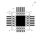
- FIG. 1 is a plan view showing an optical component mounting structure in which optical components and electronic components are mounted on an optical circuit board according to an embodiment of the present disclosure.
- 2 is an enlarged explanatory view for illustrating a cross section of a region X shown in FIG. 1 .
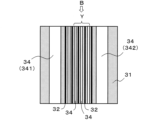
- FIG. 3 is a plan view seen from the direction of the arrow A shown in FIG. 2 (however, the upper cladding is omitted).
- 4 is an explanatory diagram for explaining a cross section of region Y as seen from the direction of arrow B shown in FIG. 3 .
- FIG. 13A to 13C are explanatory views for explaining modified examples and other arrangement examples of the recessed parts.
- 13A and 13B are explanatory diagrams for explaining modified examples regarding the depth of a recessed portion.
- FIG. 4 is an explanatory diagram for explaining another cross section of region Y as seen from the direction of arrow B shown in FIG. 3 .
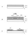
- FIG. 1A to 1C are explanatory views for explaining a process for manufacturing an optical circuit board according to an embodiment of the present disclosure.
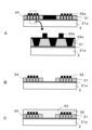
- 1A to 1C are explanatory views for explaining a process for manufacturing an optical circuit board according to an embodiment of the present disclosure.
- 1A to 1C are explanatory views for explaining a process for manufacturing an optical circuit board according to an embodiment of the present disclosure.
- the core of an optical waveguide is formed by applying a radiation-curable resin composition as the core material, pressing a mold mask having a predetermined pattern against it, and then exposing and curing it.
- a radiation-curable resin composition as the core material
- the core material becomes thick in areas where there is no pattern. This results in variations in the thickness of the core, and increases the transmission loss of the optical signal. Therefore, there is a demand for an optical circuit board that has low transmission loss of optical signals and excellent adhesion between the upper clad and the lower clad.
- the optical circuit board according to the present disclosure has a configuration as described in the section on means for solving the above problems, thereby reducing the transmission loss of optical signals and improving the adhesion between the upper clad and the lower clad. Furthermore, the manufacturing method for an optical circuit board according to the present disclosure can reduce the variation in core thickness, and can provide an optical circuit board with low transmission loss of optical signals and excellent adhesion between the upper clad and the lower clad.
- Figure 1 is a plan view showing an optical component mounting structure 10 in which an optical component 4 and an electronic component 6 are mounted on an optical circuit board 1 according to one embodiment of the present disclosure.
- the optical circuit board 1 includes a wiring board 2 and an optical waveguide 3.
- the wiring board 2 included in the optical circuit board 1 includes a wiring board that is generally used for optical circuit boards.
- Such a wiring board 2 includes, for example, a core substrate and build-up layers laminated on both sides of the core substrate, although this is not specifically illustrated.
- the core substrate is not particularly limited as long as it is made of an insulating material. Examples of insulating materials include resins such as epoxy resin, bismaleimide-triazine resin, polyimide resin, and polyphenylene ether resin. Only one type of these resins may be used, or two or more types may be used in combination.
- the core substrate usually has through-hole conductors to electrically connect the top and bottom surfaces of the core substrate.
- the core substrate may contain a reinforcing material.
- reinforcing materials include insulating fabric materials such as glass fiber, glass nonwoven fabric, aramid nonwoven fabric, aramid fiber, and polyester fiber. Only one type of reinforcing material may be used, or two or more types may be used in combination.
- the core substrate may have inorganic fillers such as silica, barium sulfate, talc, clay, glass, calcium carbonate, and titanium oxide dispersed therein. Only one type of inorganic filler may be used, or two or more types may be used in combination.
- the build-up layer has a structure in which insulating layers and conductor layers are alternately laminated.
- a part of the conductor layer located on the outermost surface includes the metal layer 21a in which the optical waveguide 3 is located.
- the conductor layer is formed of a metal such as copper.
- the insulating layer included in the build-up layer is not particularly limited as long as it is made of an insulating material, like the core board. Examples of insulating materials include resins such as epoxy resin, bismaleimide-triazine resin, polyimide resin, and polyphenylene ether resin. Only one type of these resins may be used, or two or more types may be used in combination.
- the insulating layers may be made of the same or different resins.
- the insulating layers and the core substrate included in the build-up layer may be made of the same or different resins.
- the build-up layer usually has via-hole conductors to electrically connect the layers.
- the insulating layer included in the build-up layer may contain a reinforcing material.
- reinforcing materials include insulating cloth materials such as glass fiber, glass nonwoven fabric, aramid nonwoven fabric, aramid fiber, and polyester fiber. Only one type of reinforcing material may be used, or two or more types may be used in combination.
- the insulating layer included in the build-up layer may have inorganic fillers such as silica, barium sulfate, talc, clay, glass, calcium carbonate, and titanium oxide dispersed therein. Only one type of inorganic filler may be used, or two or more types may be used in combination.
- the optical waveguide 3 included in the optical circuit board 1 is located on the surface of the metal layer 21a present on the surface of the wiring board 2.
- FIG. 2 is an enlarged explanatory diagram for explaining the cross section of region X shown in FIG. 1.
- the optical waveguide 3 has a structure in which a lower clad 31, a core 32, and an upper clad 33 are layered in this order from the metal layer 21a side.
- the lower cladding 31 included in the optical waveguide 3 is located on the surface of the wiring board 2, specifically, on the surface of the metal layer 21a present on the surface of the optical waveguide forming region of the wiring board 2.
- the material forming the lower cladding 31 is not limited, and examples include resins such as epoxy resin and silicone resin. Only one type of these resins may be used, or two or more types may be used in combination.
- the upper clad 33 included in the optical waveguide 3 is positioned so as to cover the upper surface of the lower clad 31 and the core 32.
- the upper clad 33 is also formed of a resin such as an epoxy resin or a silicone resin. Only one type of these resins may be used, or two or more types may be used in combination.
- the lower cladding 31 and the upper cladding 33 may be made of the same material or different materials. Furthermore, the lower cladding 31 and the upper cladding 33 may have the same thickness or different thicknesses. The lower cladding 31 and the upper cladding 33 each have a thickness of, for example, 5 ⁇ m or more and 200 ⁇ m or less.
- the core 32 included in the optical waveguide 3 is the portion through which the light that has entered the optical waveguide 3 propagates. Specifically, the side of the optical transmission path 41 included in the optical component 4 mounted in the mounting area of the wiring board 2 and the side of the core 32 of the optical waveguide 3 are positioned to face each other. With this configuration, optical signals are transmitted and received between the core 32 and the optical transmission path 41.
- the material forming the core 32 is not limited, and is appropriately selected, taking into consideration, for example, the light transmittance and the wavelength characteristics of the propagating light.
- Examples of the material include resins such as epoxy resin and silicone resin. Only one type of these resins may be used, or two or more types may be used in combination.
- the core 32 has a thickness of, for example, 1 ⁇ m or more and 60 ⁇ m or less.
- At least one recess 34 is located in the lower cladding 31, as shown in Figure 3.
- Figure 3 is a plan view seen from the direction of arrow A shown in Figure 2 (however, the upper cladding 33 is omitted).
- the recess 34 is located along the core 32.
- Figure 4 a part of the upper cladding 33 is located in the recess 34.
- Figure 4 is an explanatory diagram for explaining the cross section of region Y seen from the direction of arrow B shown in Figure 3.
- a portion of the upper clad 33 is located in the recess 34, increasing the adhesion area between the upper clad 33 and the lower clad 31. As a result, the adhesion between the upper clad 33 and the lower clad 31 is improved.
- the number of recesses 34 is not limited as long as there is at least one recess in the lower cladding 31.
- the recess 34 may have a first recess 341 and a second recess 342 sandwiching the core 32 in a plan view.
- the floating of the upper cladding 33 is reduced. "Floating" means that the upper cladding 33 is partially peeled off from the lower cladding 31, causing the upper cladding to float.
- multiple cores 32 may be positioned adjacent to each other, and multiple recesses 34 may be positioned to sandwich each of the multiple cores 32.
- the bonding area between the upper clad 33 and the lower clad 31 is further increased.
- the adhesion between the upper clad 33 and the lower clad 31 is further improved.
- the cross-sectional shape of the recess 34 is not limited.
- the recess 34 may have approximately the same width from the opening to the bottom of the recess 34, or may have a different width from the opening to the bottom of the recess 34.
- the width W2 of the opening of the recess 34 may be greater than the width W1 of the bottom of the recess 34.
- the width of the recess 34 may be tapered from the bottom to the opening, or may be stepped. When the width of the recess 34 is tapered from the bottom to the opening, the upper cladding 33 is easily formed in the recess 34.
- the width W2 of the opening of the recess 34 is greater than the width W1 of the bottom of the recess 34, the upper clad 33 easily enters the recess 34. This makes it easier for the upper clad 33 and the lower clad 31 to come into close contact with each other, and the adhesion between the upper clad 33 and the lower clad 31 is further improved. Furthermore, as shown in FIG. 4, the recess 34 penetrates from the top surface to the bottom surface of the lower clad 31. In such a case, reducing the width W1 of the bottom of the recess 34 increases the contact area between the lower clad 31 and the wiring board 2 (metal layer 21a). As a result, the lower clad 31 becomes less likely to peel off.
- the width W2 of the opening of the recess 34 is not limited and may be, for example, 50 ⁇ m or more and 200 ⁇ m or less.
- the width W1 of the bottom of the recess 34 is not limited and may be, for example, 40 ⁇ m or more and 190 ⁇ m or less.
- the shapes of the recesses 34 may be the same or different. For example, when viewed from above, all of the recesses 34 do not need to have the same width.
- the arithmetic mean roughness of the inner wall surface of the recess 34 is not limited, and may be, for example, greater than the arithmetic mean roughness of the upper surface of the lower cladding 31.
- the arithmetic mean roughness of the inner wall surface of the recess 34 is large, a stronger anchor effect is exerted between the inner wall surface of the recess 34 and the upper cladding 33. As a result, the adhesion between the upper cladding 33 and the lower cladding 31 is improved.
- the arithmetic mean roughness can be calculated, for example, by measuring any inner wall surface of the recess 34 and any upper surface of the lower cladding 31 with a laser displacement meter or optical interference measuring device after the lower cladding 31 is formed.
- the length of the recess 34 is not limited as long as it is positioned along the core 32.
- the length of the recess 34 may be approximately the same as the length of the core 32, as shown in FIG. 3, for example, or may be shorter than the length of the core 32.
- the recess 34 may be positioned intermittently along the core 32.
- FIG. 5 is an explanatory diagram for explaining other examples of the shape and arrangement of the recess.
- the recesses 34 have a circular shape when viewed from above, but this shape is not limited.
- the recesses 34 may be elliptical or polygonal (triangle, square, pentagon, hexagon, etc.).
- the recesses 34 may each have the same shape, size, and depth, or may have different shapes, sizes, and depths.
- continuous recesses 34 and intermittent recesses 34 may be mixed.
- the depth of the recess 34 is not limited, and may penetrate from the upper surface to the lower surface of the lower clad 31 as shown in FIG. 4, or may not penetrate as shown in FIG. 6.
- FIG. 6 is an explanatory diagram for explaining a modified example regarding the depth of the recess.
- the recess 34 has a depth of at least 20% of the thickness of the lower clad 31.
- the recess 34 penetrates from the upper surface to the lower surface of the lower clad 31.
- the metal layer 21a is exposed at the bottom of the recess 34. Therefore, the upper clad 33 located in the recess 34 comes into contact with the metal layer 21a, and the adhesive force between the upper clad 33 and the metal layer 21a is improved by the anchor effect. As a result, the upper clad 33 becomes less likely to peel off.
- the surface of the metal layer 21a is usually roughened, and has an arithmetic mean roughness of, for example, 100 nm or more and 800 nm or less.
- the upper cladding 33 may have a depression 331 in a region overlapping with the recess 34 when viewed from above, as shown in FIG. 7, for example. That is, the depression 331 of the upper cladding 33 is located in a region overlapping with the recess 34 of the lower cladding 31.
- the depression 331 is located, for example, on the surface of the upper cladding 33 as indicated by arrow C in FIG. 7. The presence of such a depression 331 makes it possible to visually confirm the approximate position of the core 32. This facilitates alignment during inspection, etc.
- the size and depth of the depression 331 are not limited as long as they are a size and depth that can be visually confirmed.
- Figures 8 to 10 are explanatory views for explaining steps for manufacturing an optical circuit-board 1 according to an embodiment of the present disclosure.
- the method for manufacturing an optical circuit-board 1 according to an embodiment includes the following steps (a) to (i). (a) A step of preparing a wiring board.
- Step (a) is a step of preparing the wiring board 2.
- the wiring board 2 is as described above, and a detailed description will be omitted.
- Step (b) is a step of forming a lower clad 31 having a recess 34 on the upper surface of the wiring board 2.
- a resin film 31a which is the material of the lower clad 31, is placed on the upper surface of the wiring board 2 (the upper surface of the metal layer 21a).
- examples of the resin film 31a include films formed from resins such as epoxy resin and silicone resin.
- the resin film 31a has a thickness of, for example, 5 ⁇ m or more and 200 ⁇ m or less, taking into account the thickness of the resulting lower clad 31.
- the metal layer 21a is formed in FIG. 8A, the metal layer 21a is not necessary.
- the resin film 31a is covered with a mold 35.
- the mold 35 is formed with a light-shielding portion 35a that acts as a mask during exposure.
- the light-shielding portion 35a is formed of a metal such as chromium or a resin.
- a recess 34 is formed in the lower clad 31. Specifically, the portion shielded by the light-shielding portion 35a does not harden and is removed by development to form the recess 34.
- Step (c) is a step of applying core resin 32a to the upper surface of lower clad 31.
- core resin 32a is applied so as to cover lower clad 31.
- examples of core resin 32a include films formed of resins such as epoxy resin and silicone resin. Taking into account the thickness of the resulting core 32, core resin 32a has a thickness of, for example, 1 ⁇ m or more and 65 ⁇ m or less.
- Step (d) is a step of preparing a light-transmitting mold 36 having a first surface 361 and a second surface 362 opposite the first surface 361, and having a core pattern groove 363 on the first surface 361 and a light-shielding portion 364 in a portion other than the core pattern groove 363.
- the core pattern groove 363 is formed on the first surface 361 of the mold 36, taking into consideration the width, height and shape of the desired core 32.
- the light-shielding portion 364 is located in a portion other than the core pattern groove 363, and is formed of a metal such as chromium.
- step (e) the mold 36 is placed so that the first surface 361 is in contact with the core resin 32a and so that the core pattern grooves 363 are aligned with but do not overlap the recesses 34 in a plan view. After the mold 36 is placed, the mold 36 is pressed in step (f).
- Step (f) is a step of pressing the mold 36 placed on the core resin 32a so that the core resin 32a is positioned in the core pattern groove 363 and the recess 34.
- pressing the mold 36 causes a portion of the core resin 32a to flow into the recess 34.
- the core resin 32a that has flowed into the recess 34 may have a recess.
- the recesses 34 are positioned so as to sandwich the core 32, when the mold 36 is pressed, the excess core resin 32a disperses and flows into each recess 34. As a result, the variation in thickness of the resulting core 32 can be reduced more efficiently.
- the proportion of the recesses 34 in the lower cladding 31 is not limited.
- the total volume of the recesses 34 may be larger than the total volume of the core 32. If the total volume of the recesses 34 is large, excess core resin 32a tends to flow into the recesses 34. As a result, the variation in thickness of the resulting core 32 can be reduced more efficiently.
- Step (g) is a step of exposing the second surface 362 of the mold 36 to light to semi-cure the core pattern groove 363 and the core resin 32a located below the core pattern groove 363.
- the exposure is performed by, for example, irradiating ultraviolet (UV) light.
- the amount (strength) of ultraviolet light and the exposure time for semi-cure the core resin 32a are appropriately set depending on the type of core resin 32a used.
- the core resin 32a covered by the light-shielding portion 364 is not semi-cure and remains uncured.
- the width of the recess 34 may increase from the bottom toward the opening. If the width of the recess 34 increases from the bottom toward the opening, excess core resin 32a will flow into the recess 34 more easily. As a result, the variation in thickness of the resulting core 32 can be reduced more efficiently.
- step (h) the mold 36 is removed, the uncured core resin 32a located on the upper surface and in the recess 34 of the lower cladding 31 is developed and removed, and then the core resin 32a is cured to form the core 32.
- the uncured core resin 32a in the portion covered by the light shielding portion 364 is developed and removed as shown in FIG. 10B.
- the remaining semi-cured core resin 32a (the portion of the core resin 32a that is not covered by the light-shielding portion 364) is cured.
- the curing is performed, for example, by irradiating it with ultraviolet light. In this way, as shown in FIG. 10B, the cores 32 are formed on the upper surface of the lower cladding 31 with reduced variation in thickness.
- Step (i) is a step of forming the upper clad 33, which covers the upper surface of the lower clad 31 and the core 32 and is located in the recess 34.
- a resin film that will be the material for the upper clad 33 is prepared.
- examples of the resin film include films formed from resins such as epoxy resin and silicone resin. Taking into account the thickness of the resulting upper clad 33, the resin film has a thickness of, for example, 5 ⁇ m or more and 250 ⁇ m or less.
- a resin film that will be the material for the upper clad 33 is placed on the top surface of the lower clad 31 and the top surface of the core 32 shown in FIG. 10B.
- the resin film is then heated and pressurized to cover the top surface of the lower clad 31 and the core 32, and is laminated so that a portion of the resin film is positioned in the recess 34, forming the upper clad 33 as shown in FIG. 10C.
- an optical component mounting structure 10 has a structure in which an optical component 4 and an electronic component 6 are mounted on an optical circuit board 1 according to an embodiment.
- the optical component 4 mounted on the optical component mounting structure 10 according to an embodiment includes an optical transmission path 41.
- optical components 4 including such optical transmission paths 41 include silicon photonics devices.
- electronic components 6 include ASICs (Application Specific Integrated Circuits) and driver ICs.
- the optical component 4 is electrically connected to the wiring board 2. Specifically, the optical component 4 is electrically connected to a pad 21b located in the mounting area (optical component mounting area) of the wiring board 2 via solder 7.
- the pad 21b is part of a conductor layer located on the upper surface of the wiring board 2.
- a silicon photonics device will be described as an example of the optical component 4.
- the silicon photonics device is a type of optical component having an optical transmission path 41 with, for example, silicon (Si) as a core and silicon dioxide (SiO 2 ) as a cladding.
- the silicon photonics device includes a Si waveguide as the optical transmission path 41, and further includes a passivation film, a light source unit, a light detection unit, and the like, although not shown.
- the optical transmission path 41 (Si waveguide 41) is located at one end of the optical waveguide 3 so as to face the core 32 included in the optical waveguide 3.
- an electrical signal from the wiring board 2 is transmitted via the solder 7 to the light source section included in the optical component 4 (silicon photonics device).
- the light source section receives the transmitted electrical signal and emits light.
- the emitted optical signal is transmitted via the optical transmission path 41 (Si waveguide 41) and the core 32 to the optical fiber 5 connected via the optical connector 5a.
- the optical circuit board includes a wiring board and an optical waveguide located on the wiring board.
- the optical waveguide includes a lower cladding, a core, and an upper cladding from the upper surface side of the wiring board.
- the core extends to the upper surface of the lower cladding.
- the upper cladding covers the upper surface of the lower cladding and the core.
- the lower cladding has at least one recess located along the core. A portion of the upper cladding is located in the recess.
- the recess has a first recess and a second recess positioned to sandwich the core therebetween.
- a plurality of cores are positioned adjacent to each other.
- a plurality of cores are positioned adjacent to each other, and a plurality of recesses are positioned so as to sandwich each of the plurality of cores therebetween.
- the recess has a bottom and an opening, and in a cross-sectional view perpendicular to the direction in which the core extends, the width of the opening of the recess is greater than the width of the bottom of the recess.
- the width of the recess increases from the bottom toward the opening.
- the arithmetic mean roughness of the inner wall surface of the recess is greater than the arithmetic mean roughness of the upper surface of the lower cladding.
- the wiring board further includes a metal layer, and the optical waveguide is located on an upper surface of the metal layer.
- the recess is located from the upper surface of the lower clad to the metal layer, and the upper clad is in contact with the metal layer.
- the upper clad has a depression in a region overlapping with the recess in a plan view.
- the optical component mounting structure according to the present disclosure includes an optical circuit board described in any one of (1) to (10) above and an optical component mounted on the optical circuit board.
- a method for manufacturing an optical circuit board includes the steps of preparing a wiring board, forming a lower clad having a recess on the upper surface of the wiring board, applying a core resin to the upper surface of the lower clad, preparing a light-transmitting mold having a first surface and a second surface opposite the first surface, a core pattern groove on the first surface, and a light-shielding portion in a portion other than the core pattern groove, placing the mold so that the first surface is in contact with the core resin and so that the core pattern groove is aligned with the recess without overlapping it in a planar perspective view, and
- the process includes a step of pressing a mold placed on the core resin so that the core resin is positioned in the turn groove and the recess; a step of exposing the mold from the second surface side to semi-cure the core resin located in the core pattern groove and the lower part of the core pattern groove; a step of removing the mold, developing and removing the uncured core resin located
- the wiring substrate further includes a metal layer, and a lower clad is formed on the metal layer.
Landscapes
- Physics & Mathematics (AREA)
- Engineering & Computer Science (AREA)
- Microelectronics & Electronic Packaging (AREA)
- General Physics & Mathematics (AREA)
- Optics & Photonics (AREA)
- Optical Integrated Circuits (AREA)
Priority Applications (1)
| Application Number | Priority Date | Filing Date | Title |
|---|---|---|---|
| JP2024561448A JPWO2024117023A1 (https=) | 2022-11-30 | 2023-11-24 |
Applications Claiming Priority (2)
| Application Number | Priority Date | Filing Date | Title |
|---|---|---|---|
| JP2022-191274 | 2022-11-30 | ||
| JP2022191274 | 2022-11-30 |
Publications (1)
| Publication Number | Publication Date |
|---|---|
| WO2024117023A1 true WO2024117023A1 (ja) | 2024-06-06 |
Family
ID=91323994
Family Applications (1)
| Application Number | Title | Priority Date | Filing Date |
|---|---|---|---|
| PCT/JP2023/042123 Ceased WO2024117023A1 (ja) | 2022-11-30 | 2023-11-24 | 光回路基板、光学部品実装構造体および光回路基板の製造方法 |
Country Status (3)
| Country | Link |
|---|---|
| JP (1) | JPWO2024117023A1 (https=) |
| TW (1) | TW202430946A (https=) |
| WO (1) | WO2024117023A1 (https=) |
Citations (8)
| Publication number | Priority date | Publication date | Assignee | Title |
|---|---|---|---|---|
| JPH01198706A (ja) * | 1987-12-02 | 1989-08-10 | Furukawa Electric Co Ltd:The | 埋め込み型光導波路 |
| JP2004233406A (ja) * | 2003-01-28 | 2004-08-19 | Fuji Xerox Co Ltd | 光導波路基板の製造方法、光導波路基板、及び光反射構造体 |
| JP2004295118A (ja) * | 2003-03-12 | 2004-10-21 | Sanyo Electric Co Ltd | 光導波路 |
| JP2008262003A (ja) * | 2007-04-11 | 2008-10-30 | Sumitomo Electric Ind Ltd | 光導波路および光導波路製造方法 |
| JP2011007886A (ja) * | 2009-06-23 | 2011-01-13 | Nippon Shokubai Co Ltd | 光導波路の製造方法およびそれに用いる型 |
| US20150003778A1 (en) * | 2011-12-08 | 2015-01-01 | Lg Innotek Co., Ltd. | Optical printed circuit board and method of manufacturing the same |
| US20150192735A1 (en) * | 2014-01-09 | 2015-07-09 | International Business Machines Corporation | Shielding structures between optical waveguides |
| JP2019082576A (ja) * | 2017-10-31 | 2019-05-30 | 日本電信電話株式会社 | 光導波路およびその製造方法 |
-
2023
- 2023-11-24 WO PCT/JP2023/042123 patent/WO2024117023A1/ja not_active Ceased
- 2023-11-24 JP JP2024561448A patent/JPWO2024117023A1/ja active Pending
- 2023-11-30 TW TW112146618A patent/TW202430946A/zh unknown
Patent Citations (8)
| Publication number | Priority date | Publication date | Assignee | Title |
|---|---|---|---|---|
| JPH01198706A (ja) * | 1987-12-02 | 1989-08-10 | Furukawa Electric Co Ltd:The | 埋め込み型光導波路 |
| JP2004233406A (ja) * | 2003-01-28 | 2004-08-19 | Fuji Xerox Co Ltd | 光導波路基板の製造方法、光導波路基板、及び光反射構造体 |
| JP2004295118A (ja) * | 2003-03-12 | 2004-10-21 | Sanyo Electric Co Ltd | 光導波路 |
| JP2008262003A (ja) * | 2007-04-11 | 2008-10-30 | Sumitomo Electric Ind Ltd | 光導波路および光導波路製造方法 |
| JP2011007886A (ja) * | 2009-06-23 | 2011-01-13 | Nippon Shokubai Co Ltd | 光導波路の製造方法およびそれに用いる型 |
| US20150003778A1 (en) * | 2011-12-08 | 2015-01-01 | Lg Innotek Co., Ltd. | Optical printed circuit board and method of manufacturing the same |
| US20150192735A1 (en) * | 2014-01-09 | 2015-07-09 | International Business Machines Corporation | Shielding structures between optical waveguides |
| JP2019082576A (ja) * | 2017-10-31 | 2019-05-30 | 日本電信電話株式会社 | 光導波路およびその製造方法 |
Also Published As
| Publication number | Publication date |
|---|---|
| TW202430946A (zh) | 2024-08-01 |
| JPWO2024117023A1 (https=) | 2024-06-06 |
Similar Documents
| Publication | Publication Date | Title |
|---|---|---|
| JP7617248B2 (ja) | 光回路基板およびそれを用いた光学部品実装構造体 | |
| KR20100133767A (ko) | 광도파로용 인쇄회로기판 및 그 제조방법 | |
| US20090065132A1 (en) | Method of forming optical waveguide | |
| JP7744501B2 (ja) | 光回路基板 | |
| JP7515609B2 (ja) | 光回路基板およびそれを用いた電子部品実装構造体 | |
| CN101605428B (zh) | 具有光波导层的线路板及其制造方法 | |
| WO2024117023A1 (ja) | 光回路基板、光学部品実装構造体および光回路基板の製造方法 | |
| JP7818626B2 (ja) | 光回路基板および光学部品実装構造体 | |
| JP7738133B2 (ja) | 光回路基板 | |
| US12481109B2 (en) | Optical circuit board and electronic component mounting structure using the same | |
| JP7710784B2 (ja) | 光回路基板および光学部品実装構造体 | |
| JP7813873B2 (ja) | 光回路基板 | |
| WO2025205531A1 (ja) | 光回路基板および実装構造体 | |
| TWI917915B (zh) | 光迴路基板及安裝構造體 | |
| JP7788203B2 (ja) | 光回路基板およびそれを用いた光学部品実装構造体 | |
| WO2024204111A1 (ja) | 光回路基板および実装構造体 | |
| JP2002022976A (ja) | 光・電子プリント配線板およびその製造方法 | |
| WO2025183093A1 (ja) | 光回路基板および実装構造体 | |
| WO2025182787A1 (ja) | 光回路基板および実装構造体 | |
| WO2024143134A1 (ja) | 光回路基板、光学部品実装構造体および光回路基板の製造方法 | |
| WO2025206001A1 (ja) | 光回路基板および実装構造体 |
Legal Events
| Date | Code | Title | Description |
|---|---|---|---|
| 121 | Ep: the epo has been informed by wipo that ep was designated in this application |
Ref document number: 23897671 Country of ref document: EP Kind code of ref document: A1 |
|
| WWE | Wipo information: entry into national phase |
Ref document number: 2024561448 Country of ref document: JP |
|
| NENP | Non-entry into the national phase |
Ref country code: DE |
|
| 122 | Ep: pct application non-entry in european phase |
Ref document number: 23897671 Country of ref document: EP Kind code of ref document: A1 |