WO2024117023A1 - Optical circuit board, optical component mounting structure, and method for manufacturing optical circuit board - Google Patents
Optical circuit board, optical component mounting structure, and method for manufacturing optical circuit board Download PDFInfo
- Publication number
- WO2024117023A1 WO2024117023A1 PCT/JP2023/042123 JP2023042123W WO2024117023A1 WO 2024117023 A1 WO2024117023 A1 WO 2024117023A1 JP 2023042123 W JP2023042123 W JP 2023042123W WO 2024117023 A1 WO2024117023 A1 WO 2024117023A1
- Authority
- WO
- WIPO (PCT)
- Prior art keywords
- core
- recess
- circuit board
- optical circuit
- optical
- Prior art date
Links
- 230000003287 optical effect Effects 0.000 title claims abstract description 138
- 238000000034 method Methods 0.000 title claims description 15
- 238000004519 manufacturing process Methods 0.000 title claims description 14
- 229920005989 resin Polymers 0.000 claims description 82
- 239000011347 resin Substances 0.000 claims description 82
- 238000005253 cladding Methods 0.000 claims description 51
- 229910052751 metal Inorganic materials 0.000 claims description 30
- 239000002184 metal Substances 0.000 claims description 30
- 239000000758 substrate Substances 0.000 claims description 12
- 238000003825 pressing Methods 0.000 claims description 8
- 239000011162 core material Substances 0.000 description 146
- 230000005540 biological transmission Effects 0.000 description 15
- 239000000463 material Substances 0.000 description 10
- 239000003822 epoxy resin Substances 0.000 description 8
- 229920000647 polyepoxide Polymers 0.000 description 8
- XUIMIQQOPSSXEZ-UHFFFAOYSA-N Silicon Chemical compound [Si] XUIMIQQOPSSXEZ-UHFFFAOYSA-N 0.000 description 7
- 239000004020 conductor Substances 0.000 description 7
- 238000010586 diagram Methods 0.000 description 7
- 229910052710 silicon Inorganic materials 0.000 description 7
- 239000010703 silicon Substances 0.000 description 7
- VYPSYNLAJGMNEJ-UHFFFAOYSA-N Silicium dioxide Chemical compound O=[Si]=O VYPSYNLAJGMNEJ-UHFFFAOYSA-N 0.000 description 6
- 239000012779 reinforcing material Substances 0.000 description 6
- 229920002050 silicone resin Polymers 0.000 description 6
- VTYYLEPIZMXCLO-UHFFFAOYSA-L Calcium carbonate Chemical compound [Ca+2].[O-]C([O-])=O VTYYLEPIZMXCLO-UHFFFAOYSA-L 0.000 description 4
- TZCXTZWJZNENPQ-UHFFFAOYSA-L barium sulfate Chemical compound [Ba+2].[O-]S([O-])(=O)=O TZCXTZWJZNENPQ-UHFFFAOYSA-L 0.000 description 4
- 239000011521 glass Substances 0.000 description 4
- 239000011256 inorganic filler Substances 0.000 description 4
- 229910003475 inorganic filler Inorganic materials 0.000 description 4
- 239000011810 insulating material Substances 0.000 description 4
- 239000004745 nonwoven fabric Substances 0.000 description 4
- 239000013307 optical fiber Substances 0.000 description 4
- 239000000377 silicon dioxide Substances 0.000 description 3
- 229910000679 solder Inorganic materials 0.000 description 3
- VYZAMTAEIAYCRO-UHFFFAOYSA-N Chromium Chemical compound [Cr] VYZAMTAEIAYCRO-UHFFFAOYSA-N 0.000 description 2
- GWEVSGVZZGPLCZ-UHFFFAOYSA-N Titan oxide Chemical compound O=[Ti]=O GWEVSGVZZGPLCZ-UHFFFAOYSA-N 0.000 description 2
- 239000000853 adhesive Substances 0.000 description 2
- 230000001070 adhesive effect Effects 0.000 description 2
- 239000004760 aramid Substances 0.000 description 2
- 229920006231 aramid fiber Polymers 0.000 description 2
- 229920003235 aromatic polyamide Polymers 0.000 description 2
- 229910000019 calcium carbonate Inorganic materials 0.000 description 2
- 229910052804 chromium Inorganic materials 0.000 description 2
- 239000011651 chromium Substances 0.000 description 2
- 239000004927 clay Substances 0.000 description 2
- 229910052570 clay Inorganic materials 0.000 description 2
- 230000000694 effects Effects 0.000 description 2
- 239000004744 fabric Substances 0.000 description 2
- 239000000835 fiber Substances 0.000 description 2
- 239000003365 glass fiber Substances 0.000 description 2
- 230000001678 irradiating effect Effects 0.000 description 2
- 239000000203 mixture Substances 0.000 description 2
- 229920000728 polyester Polymers 0.000 description 2
- 229920001721 polyimide Polymers 0.000 description 2
- 239000009719 polyimide resin Substances 0.000 description 2
- 229920001955 polyphenylene ether Polymers 0.000 description 2
- 239000011342 resin composition Substances 0.000 description 2
- 239000000454 talc Substances 0.000 description 2
- 229910052623 talc Inorganic materials 0.000 description 2
- OGIDPMRJRNCKJF-UHFFFAOYSA-N titanium oxide Inorganic materials [Ti]=O OGIDPMRJRNCKJF-UHFFFAOYSA-N 0.000 description 2
- RYGMFSIKBFXOCR-UHFFFAOYSA-N Copper Chemical compound [Cu] RYGMFSIKBFXOCR-UHFFFAOYSA-N 0.000 description 1
- 229910004298 SiO 2 Inorganic materials 0.000 description 1
- 229910052802 copper Inorganic materials 0.000 description 1
- 239000010949 copper Substances 0.000 description 1
- 238000001514 detection method Methods 0.000 description 1
- 238000006073 displacement reaction Methods 0.000 description 1
- 238000007689 inspection Methods 0.000 description 1
- 239000000155 melt Substances 0.000 description 1
- 238000012986 modification Methods 0.000 description 1
- 230000004048 modification Effects 0.000 description 1
- 238000002161 passivation Methods 0.000 description 1
- 230000001902 propagating effect Effects 0.000 description 1
- 235000012239 silicon dioxide Nutrition 0.000 description 1
- 238000002834 transmittance Methods 0.000 description 1
Images


Classifications
-
- G—PHYSICS
- G02—OPTICS
- G02B—OPTICAL ELEMENTS, SYSTEMS OR APPARATUS
- G02B6/00—Light guides; Structural details of arrangements comprising light guides and other optical elements, e.g. couplings
- G02B6/10—Light guides; Structural details of arrangements comprising light guides and other optical elements, e.g. couplings of the optical waveguide type
- G02B6/12—Light guides; Structural details of arrangements comprising light guides and other optical elements, e.g. couplings of the optical waveguide type of the integrated circuit kind
- G02B6/122—Basic optical elements, e.g. light-guiding paths
-
- G—PHYSICS
- G02—OPTICS
- G02B—OPTICAL ELEMENTS, SYSTEMS OR APPARATUS
- G02B6/00—Light guides; Structural details of arrangements comprising light guides and other optical elements, e.g. couplings
- G02B6/10—Light guides; Structural details of arrangements comprising light guides and other optical elements, e.g. couplings of the optical waveguide type
- G02B6/12—Light guides; Structural details of arrangements comprising light guides and other optical elements, e.g. couplings of the optical waveguide type of the integrated circuit kind
- G02B6/13—Integrated optical circuits characterised by the manufacturing method
Definitions
- This disclosure relates to an optical circuit board, an optical component mounting structure using an optical circuit board, and a method for manufacturing an optical circuit board.
- optical fibers capable of transmitting large volumes of data at high speeds have come to be used in information communications.
- Optical signals are transmitted and received between these optical fibers and optical components.
- Such optical components are mounted on, for example, optical circuit boards.
- Optical circuit boards are equipped with optical waveguides. Optical signals are transmitted and received via these optical waveguides.
- the core of an optical waveguide is formed by applying a radiation-curable resin composition, which is the core material, pressing a mold mask having a predetermined pattern onto the composition, and then exposing and curing the composition.
- the optical circuit board includes a wiring board and an optical waveguide located on the wiring board.
- the optical waveguide includes a lower clad, a core, and an upper clad from the upper surface side of the wiring board.
- the core extends to the upper surface of the lower clad.
- the upper clad covers the upper surface of the lower clad and the core.
- the lower clad has at least one recess located along the core. A portion of the upper clad is located in the recess.
- the optical component mounting structure according to the present disclosure includes the optical circuit board described above and an optical component mounted on the optical circuit board.
- the method for manufacturing an optical circuit board includes the steps of preparing a wiring board, forming a lower clad having a recess on the upper surface of the wiring board, applying a core resin to the upper surface of the lower clad, preparing a light-transmitting mold having a first surface and a second surface opposite the first surface, a core pattern groove on the first surface, and a light-shielding portion in a portion other than the core pattern groove, placing the mold so that the first surface is in contact with the core resin and so that the core pattern groove is aligned with the recess without overlapping it in a planar perspective view, and forming a core pattern.
- the process includes a step of pressing a mold placed on the core resin so that the core resin is positioned in the groove for the core pattern and the recess; a step of exposing the mold from the second surface side to light, semi-curing the core resin located in the groove for the core pattern and the lower part of the groove for the core pattern; a step of removing the mold, developing and removing the uncured core resin located on the upper surface of the lower clad and in the recess, and then curing the core resin to form a core; and a step of covering the upper surface of the lower clad and the core, and forming an upper clad located in the recess.
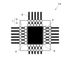
- FIG. 1 is a plan view showing an optical component mounting structure in which optical components and electronic components are mounted on an optical circuit board according to an embodiment of the present disclosure.
- 2 is an enlarged explanatory view for illustrating a cross section of a region X shown in FIG. 1 .
- FIG. 3 is a plan view seen from the direction of the arrow A shown in FIG. 2 (however, the upper cladding is omitted).
- 4 is an explanatory diagram for explaining a cross section of region Y as seen from the direction of arrow B shown in FIG. 3 .
- FIG. 13A to 13C are explanatory views for explaining modified examples and other arrangement examples of the recessed parts.
- 13A and 13B are explanatory diagrams for explaining modified examples regarding the depth of a recessed portion.
- FIG. 4 is an explanatory diagram for explaining another cross section of region Y as seen from the direction of arrow B shown in FIG. 3 .
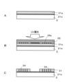
- FIG. 1A to 1C are explanatory views for explaining a process for manufacturing an optical circuit board according to an embodiment of the present disclosure.
- 1A to 1C are explanatory views for explaining a process for manufacturing an optical circuit board according to an embodiment of the present disclosure.
- 1A to 1C are explanatory views for explaining a process for manufacturing an optical circuit board according to an embodiment of the present disclosure.
- the core of an optical waveguide is formed by applying a radiation-curable resin composition as the core material, pressing a mold mask having a predetermined pattern against it, and then exposing and curing it.
- a radiation-curable resin composition as the core material
- the core material becomes thick in areas where there is no pattern. This results in variations in the thickness of the core, and increases the transmission loss of the optical signal. Therefore, there is a demand for an optical circuit board that has low transmission loss of optical signals and excellent adhesion between the upper clad and the lower clad.
- the optical circuit board according to the present disclosure has a configuration as described in the section on means for solving the above problems, thereby reducing the transmission loss of optical signals and improving the adhesion between the upper clad and the lower clad. Furthermore, the manufacturing method for an optical circuit board according to the present disclosure can reduce the variation in core thickness, and can provide an optical circuit board with low transmission loss of optical signals and excellent adhesion between the upper clad and the lower clad.
- Figure 1 is a plan view showing an optical component mounting structure 10 in which an optical component 4 and an electronic component 6 are mounted on an optical circuit board 1 according to one embodiment of the present disclosure.
- the optical circuit board 1 includes a wiring board 2 and an optical waveguide 3.
- the wiring board 2 included in the optical circuit board 1 includes a wiring board that is generally used for optical circuit boards.
- Such a wiring board 2 includes, for example, a core substrate and build-up layers laminated on both sides of the core substrate, although this is not specifically illustrated.
- the core substrate is not particularly limited as long as it is made of an insulating material. Examples of insulating materials include resins such as epoxy resin, bismaleimide-triazine resin, polyimide resin, and polyphenylene ether resin. Only one type of these resins may be used, or two or more types may be used in combination.
- the core substrate usually has through-hole conductors to electrically connect the top and bottom surfaces of the core substrate.
- the core substrate may contain a reinforcing material.
- reinforcing materials include insulating fabric materials such as glass fiber, glass nonwoven fabric, aramid nonwoven fabric, aramid fiber, and polyester fiber. Only one type of reinforcing material may be used, or two or more types may be used in combination.
- the core substrate may have inorganic fillers such as silica, barium sulfate, talc, clay, glass, calcium carbonate, and titanium oxide dispersed therein. Only one type of inorganic filler may be used, or two or more types may be used in combination.
- the build-up layer has a structure in which insulating layers and conductor layers are alternately laminated.
- a part of the conductor layer located on the outermost surface includes the metal layer 21a in which the optical waveguide 3 is located.
- the conductor layer is formed of a metal such as copper.
- the insulating layer included in the build-up layer is not particularly limited as long as it is made of an insulating material, like the core board. Examples of insulating materials include resins such as epoxy resin, bismaleimide-triazine resin, polyimide resin, and polyphenylene ether resin. Only one type of these resins may be used, or two or more types may be used in combination.
- the insulating layers may be made of the same or different resins.
- the insulating layers and the core substrate included in the build-up layer may be made of the same or different resins.
- the build-up layer usually has via-hole conductors to electrically connect the layers.
- the insulating layer included in the build-up layer may contain a reinforcing material.
- reinforcing materials include insulating cloth materials such as glass fiber, glass nonwoven fabric, aramid nonwoven fabric, aramid fiber, and polyester fiber. Only one type of reinforcing material may be used, or two or more types may be used in combination.
- the insulating layer included in the build-up layer may have inorganic fillers such as silica, barium sulfate, talc, clay, glass, calcium carbonate, and titanium oxide dispersed therein. Only one type of inorganic filler may be used, or two or more types may be used in combination.
- the optical waveguide 3 included in the optical circuit board 1 is located on the surface of the metal layer 21a present on the surface of the wiring board 2.
- FIG. 2 is an enlarged explanatory diagram for explaining the cross section of region X shown in FIG. 1.
- the optical waveguide 3 has a structure in which a lower clad 31, a core 32, and an upper clad 33 are layered in this order from the metal layer 21a side.
- the lower cladding 31 included in the optical waveguide 3 is located on the surface of the wiring board 2, specifically, on the surface of the metal layer 21a present on the surface of the optical waveguide forming region of the wiring board 2.
- the material forming the lower cladding 31 is not limited, and examples include resins such as epoxy resin and silicone resin. Only one type of these resins may be used, or two or more types may be used in combination.
- the upper clad 33 included in the optical waveguide 3 is positioned so as to cover the upper surface of the lower clad 31 and the core 32.
- the upper clad 33 is also formed of a resin such as an epoxy resin or a silicone resin. Only one type of these resins may be used, or two or more types may be used in combination.
- the lower cladding 31 and the upper cladding 33 may be made of the same material or different materials. Furthermore, the lower cladding 31 and the upper cladding 33 may have the same thickness or different thicknesses. The lower cladding 31 and the upper cladding 33 each have a thickness of, for example, 5 ⁇ m or more and 200 ⁇ m or less.
- the core 32 included in the optical waveguide 3 is the portion through which the light that has entered the optical waveguide 3 propagates. Specifically, the side of the optical transmission path 41 included in the optical component 4 mounted in the mounting area of the wiring board 2 and the side of the core 32 of the optical waveguide 3 are positioned to face each other. With this configuration, optical signals are transmitted and received between the core 32 and the optical transmission path 41.
- the material forming the core 32 is not limited, and is appropriately selected, taking into consideration, for example, the light transmittance and the wavelength characteristics of the propagating light.
- Examples of the material include resins such as epoxy resin and silicone resin. Only one type of these resins may be used, or two or more types may be used in combination.
- the core 32 has a thickness of, for example, 1 ⁇ m or more and 60 ⁇ m or less.
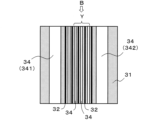
- At least one recess 34 is located in the lower cladding 31, as shown in Figure 3.
- Figure 3 is a plan view seen from the direction of arrow A shown in Figure 2 (however, the upper cladding 33 is omitted).
- the recess 34 is located along the core 32.
- Figure 4 a part of the upper cladding 33 is located in the recess 34.
- Figure 4 is an explanatory diagram for explaining the cross section of region Y seen from the direction of arrow B shown in Figure 3.
- a portion of the upper clad 33 is located in the recess 34, increasing the adhesion area between the upper clad 33 and the lower clad 31. As a result, the adhesion between the upper clad 33 and the lower clad 31 is improved.
- the number of recesses 34 is not limited as long as there is at least one recess in the lower cladding 31.
- the recess 34 may have a first recess 341 and a second recess 342 sandwiching the core 32 in a plan view.
- the floating of the upper cladding 33 is reduced. "Floating" means that the upper cladding 33 is partially peeled off from the lower cladding 31, causing the upper cladding to float.
- multiple cores 32 may be positioned adjacent to each other, and multiple recesses 34 may be positioned to sandwich each of the multiple cores 32.
- the bonding area between the upper clad 33 and the lower clad 31 is further increased.
- the adhesion between the upper clad 33 and the lower clad 31 is further improved.
- the cross-sectional shape of the recess 34 is not limited.
- the recess 34 may have approximately the same width from the opening to the bottom of the recess 34, or may have a different width from the opening to the bottom of the recess 34.
- the width W2 of the opening of the recess 34 may be greater than the width W1 of the bottom of the recess 34.
- the width of the recess 34 may be tapered from the bottom to the opening, or may be stepped. When the width of the recess 34 is tapered from the bottom to the opening, the upper cladding 33 is easily formed in the recess 34.
- the width W2 of the opening of the recess 34 is greater than the width W1 of the bottom of the recess 34, the upper clad 33 easily enters the recess 34. This makes it easier for the upper clad 33 and the lower clad 31 to come into close contact with each other, and the adhesion between the upper clad 33 and the lower clad 31 is further improved. Furthermore, as shown in FIG. 4, the recess 34 penetrates from the top surface to the bottom surface of the lower clad 31. In such a case, reducing the width W1 of the bottom of the recess 34 increases the contact area between the lower clad 31 and the wiring board 2 (metal layer 21a). As a result, the lower clad 31 becomes less likely to peel off.
- the width W2 of the opening of the recess 34 is not limited and may be, for example, 50 ⁇ m or more and 200 ⁇ m or less.
- the width W1 of the bottom of the recess 34 is not limited and may be, for example, 40 ⁇ m or more and 190 ⁇ m or less.
- the shapes of the recesses 34 may be the same or different. For example, when viewed from above, all of the recesses 34 do not need to have the same width.
- the arithmetic mean roughness of the inner wall surface of the recess 34 is not limited, and may be, for example, greater than the arithmetic mean roughness of the upper surface of the lower cladding 31.
- the arithmetic mean roughness of the inner wall surface of the recess 34 is large, a stronger anchor effect is exerted between the inner wall surface of the recess 34 and the upper cladding 33. As a result, the adhesion between the upper cladding 33 and the lower cladding 31 is improved.
- the arithmetic mean roughness can be calculated, for example, by measuring any inner wall surface of the recess 34 and any upper surface of the lower cladding 31 with a laser displacement meter or optical interference measuring device after the lower cladding 31 is formed.
- the length of the recess 34 is not limited as long as it is positioned along the core 32.
- the length of the recess 34 may be approximately the same as the length of the core 32, as shown in FIG. 3, for example, or may be shorter than the length of the core 32.
- the recess 34 may be positioned intermittently along the core 32.
- FIG. 5 is an explanatory diagram for explaining other examples of the shape and arrangement of the recess.
- the recesses 34 have a circular shape when viewed from above, but this shape is not limited.
- the recesses 34 may be elliptical or polygonal (triangle, square, pentagon, hexagon, etc.).
- the recesses 34 may each have the same shape, size, and depth, or may have different shapes, sizes, and depths.
- continuous recesses 34 and intermittent recesses 34 may be mixed.
- the depth of the recess 34 is not limited, and may penetrate from the upper surface to the lower surface of the lower clad 31 as shown in FIG. 4, or may not penetrate as shown in FIG. 6.
- FIG. 6 is an explanatory diagram for explaining a modified example regarding the depth of the recess.
- the recess 34 has a depth of at least 20% of the thickness of the lower clad 31.
- the recess 34 penetrates from the upper surface to the lower surface of the lower clad 31.
- the metal layer 21a is exposed at the bottom of the recess 34. Therefore, the upper clad 33 located in the recess 34 comes into contact with the metal layer 21a, and the adhesive force between the upper clad 33 and the metal layer 21a is improved by the anchor effect. As a result, the upper clad 33 becomes less likely to peel off.
- the surface of the metal layer 21a is usually roughened, and has an arithmetic mean roughness of, for example, 100 nm or more and 800 nm or less.
- the upper cladding 33 may have a depression 331 in a region overlapping with the recess 34 when viewed from above, as shown in FIG. 7, for example. That is, the depression 331 of the upper cladding 33 is located in a region overlapping with the recess 34 of the lower cladding 31.
- the depression 331 is located, for example, on the surface of the upper cladding 33 as indicated by arrow C in FIG. 7. The presence of such a depression 331 makes it possible to visually confirm the approximate position of the core 32. This facilitates alignment during inspection, etc.
- the size and depth of the depression 331 are not limited as long as they are a size and depth that can be visually confirmed.
- Figures 8 to 10 are explanatory views for explaining steps for manufacturing an optical circuit-board 1 according to an embodiment of the present disclosure.
- the method for manufacturing an optical circuit-board 1 according to an embodiment includes the following steps (a) to (i). (a) A step of preparing a wiring board.
- Step (a) is a step of preparing the wiring board 2.
- the wiring board 2 is as described above, and a detailed description will be omitted.
- Step (b) is a step of forming a lower clad 31 having a recess 34 on the upper surface of the wiring board 2.
- a resin film 31a which is the material of the lower clad 31, is placed on the upper surface of the wiring board 2 (the upper surface of the metal layer 21a).
- examples of the resin film 31a include films formed from resins such as epoxy resin and silicone resin.
- the resin film 31a has a thickness of, for example, 5 ⁇ m or more and 200 ⁇ m or less, taking into account the thickness of the resulting lower clad 31.
- the metal layer 21a is formed in FIG. 8A, the metal layer 21a is not necessary.
- the resin film 31a is covered with a mold 35.
- the mold 35 is formed with a light-shielding portion 35a that acts as a mask during exposure.
- the light-shielding portion 35a is formed of a metal such as chromium or a resin.
- a recess 34 is formed in the lower clad 31. Specifically, the portion shielded by the light-shielding portion 35a does not harden and is removed by development to form the recess 34.
- Step (c) is a step of applying core resin 32a to the upper surface of lower clad 31.
- core resin 32a is applied so as to cover lower clad 31.
- examples of core resin 32a include films formed of resins such as epoxy resin and silicone resin. Taking into account the thickness of the resulting core 32, core resin 32a has a thickness of, for example, 1 ⁇ m or more and 65 ⁇ m or less.
- Step (d) is a step of preparing a light-transmitting mold 36 having a first surface 361 and a second surface 362 opposite the first surface 361, and having a core pattern groove 363 on the first surface 361 and a light-shielding portion 364 in a portion other than the core pattern groove 363.
- the core pattern groove 363 is formed on the first surface 361 of the mold 36, taking into consideration the width, height and shape of the desired core 32.
- the light-shielding portion 364 is located in a portion other than the core pattern groove 363, and is formed of a metal such as chromium.
- step (e) the mold 36 is placed so that the first surface 361 is in contact with the core resin 32a and so that the core pattern grooves 363 are aligned with but do not overlap the recesses 34 in a plan view. After the mold 36 is placed, the mold 36 is pressed in step (f).
- Step (f) is a step of pressing the mold 36 placed on the core resin 32a so that the core resin 32a is positioned in the core pattern groove 363 and the recess 34.
- pressing the mold 36 causes a portion of the core resin 32a to flow into the recess 34.
- the core resin 32a that has flowed into the recess 34 may have a recess.
- the recesses 34 are positioned so as to sandwich the core 32, when the mold 36 is pressed, the excess core resin 32a disperses and flows into each recess 34. As a result, the variation in thickness of the resulting core 32 can be reduced more efficiently.
- the proportion of the recesses 34 in the lower cladding 31 is not limited.
- the total volume of the recesses 34 may be larger than the total volume of the core 32. If the total volume of the recesses 34 is large, excess core resin 32a tends to flow into the recesses 34. As a result, the variation in thickness of the resulting core 32 can be reduced more efficiently.
- Step (g) is a step of exposing the second surface 362 of the mold 36 to light to semi-cure the core pattern groove 363 and the core resin 32a located below the core pattern groove 363.
- the exposure is performed by, for example, irradiating ultraviolet (UV) light.
- the amount (strength) of ultraviolet light and the exposure time for semi-cure the core resin 32a are appropriately set depending on the type of core resin 32a used.
- the core resin 32a covered by the light-shielding portion 364 is not semi-cure and remains uncured.
- the width of the recess 34 may increase from the bottom toward the opening. If the width of the recess 34 increases from the bottom toward the opening, excess core resin 32a will flow into the recess 34 more easily. As a result, the variation in thickness of the resulting core 32 can be reduced more efficiently.
- step (h) the mold 36 is removed, the uncured core resin 32a located on the upper surface and in the recess 34 of the lower cladding 31 is developed and removed, and then the core resin 32a is cured to form the core 32.
- the uncured core resin 32a in the portion covered by the light shielding portion 364 is developed and removed as shown in FIG. 10B.
- the remaining semi-cured core resin 32a (the portion of the core resin 32a that is not covered by the light-shielding portion 364) is cured.
- the curing is performed, for example, by irradiating it with ultraviolet light. In this way, as shown in FIG. 10B, the cores 32 are formed on the upper surface of the lower cladding 31 with reduced variation in thickness.
- Step (i) is a step of forming the upper clad 33, which covers the upper surface of the lower clad 31 and the core 32 and is located in the recess 34.
- a resin film that will be the material for the upper clad 33 is prepared.
- examples of the resin film include films formed from resins such as epoxy resin and silicone resin. Taking into account the thickness of the resulting upper clad 33, the resin film has a thickness of, for example, 5 ⁇ m or more and 250 ⁇ m or less.
- a resin film that will be the material for the upper clad 33 is placed on the top surface of the lower clad 31 and the top surface of the core 32 shown in FIG. 10B.
- the resin film is then heated and pressurized to cover the top surface of the lower clad 31 and the core 32, and is laminated so that a portion of the resin film is positioned in the recess 34, forming the upper clad 33 as shown in FIG. 10C.
- an optical component mounting structure 10 has a structure in which an optical component 4 and an electronic component 6 are mounted on an optical circuit board 1 according to an embodiment.
- the optical component 4 mounted on the optical component mounting structure 10 according to an embodiment includes an optical transmission path 41.
- optical components 4 including such optical transmission paths 41 include silicon photonics devices.
- electronic components 6 include ASICs (Application Specific Integrated Circuits) and driver ICs.
- the optical component 4 is electrically connected to the wiring board 2. Specifically, the optical component 4 is electrically connected to a pad 21b located in the mounting area (optical component mounting area) of the wiring board 2 via solder 7.
- the pad 21b is part of a conductor layer located on the upper surface of the wiring board 2.
- a silicon photonics device will be described as an example of the optical component 4.
- the silicon photonics device is a type of optical component having an optical transmission path 41 with, for example, silicon (Si) as a core and silicon dioxide (SiO 2 ) as a cladding.
- the silicon photonics device includes a Si waveguide as the optical transmission path 41, and further includes a passivation film, a light source unit, a light detection unit, and the like, although not shown.
- the optical transmission path 41 (Si waveguide 41) is located at one end of the optical waveguide 3 so as to face the core 32 included in the optical waveguide 3.
- an electrical signal from the wiring board 2 is transmitted via the solder 7 to the light source section included in the optical component 4 (silicon photonics device).
- the light source section receives the transmitted electrical signal and emits light.
- the emitted optical signal is transmitted via the optical transmission path 41 (Si waveguide 41) and the core 32 to the optical fiber 5 connected via the optical connector 5a.
- the optical circuit board includes a wiring board and an optical waveguide located on the wiring board.
- the optical waveguide includes a lower cladding, a core, and an upper cladding from the upper surface side of the wiring board.
- the core extends to the upper surface of the lower cladding.
- the upper cladding covers the upper surface of the lower cladding and the core.
- the lower cladding has at least one recess located along the core. A portion of the upper cladding is located in the recess.
- the recess has a first recess and a second recess positioned to sandwich the core therebetween.
- a plurality of cores are positioned adjacent to each other.
- a plurality of cores are positioned adjacent to each other, and a plurality of recesses are positioned so as to sandwich each of the plurality of cores therebetween.
- the recess has a bottom and an opening, and in a cross-sectional view perpendicular to the direction in which the core extends, the width of the opening of the recess is greater than the width of the bottom of the recess.
- the width of the recess increases from the bottom toward the opening.
- the arithmetic mean roughness of the inner wall surface of the recess is greater than the arithmetic mean roughness of the upper surface of the lower cladding.
- the wiring board further includes a metal layer, and the optical waveguide is located on an upper surface of the metal layer.
- the recess is located from the upper surface of the lower clad to the metal layer, and the upper clad is in contact with the metal layer.
- the upper clad has a depression in a region overlapping with the recess in a plan view.
- the optical component mounting structure according to the present disclosure includes an optical circuit board described in any one of (1) to (10) above and an optical component mounted on the optical circuit board.
- a method for manufacturing an optical circuit board includes the steps of preparing a wiring board, forming a lower clad having a recess on the upper surface of the wiring board, applying a core resin to the upper surface of the lower clad, preparing a light-transmitting mold having a first surface and a second surface opposite the first surface, a core pattern groove on the first surface, and a light-shielding portion in a portion other than the core pattern groove, placing the mold so that the first surface is in contact with the core resin and so that the core pattern groove is aligned with the recess without overlapping it in a planar perspective view, and
- the process includes a step of pressing a mold placed on the core resin so that the core resin is positioned in the turn groove and the recess; a step of exposing the mold from the second surface side to semi-cure the core resin located in the core pattern groove and the lower part of the core pattern groove; a step of removing the mold, developing and removing the uncured core resin located
- the wiring substrate further includes a metal layer, and a lower clad is formed on the metal layer.
Landscapes
- Physics & Mathematics (AREA)
- Engineering & Computer Science (AREA)
- Microelectronics & Electronic Packaging (AREA)
- General Physics & Mathematics (AREA)
- Optics & Photonics (AREA)
- Optical Integrated Circuits (AREA)
Abstract
An optical circuit board (1) according to the present disclosure comprises: a wiring board (2); and an optical waveguide (3) located on the wiring board (2). The optical waveguide (3) includes a lower clad (31), a core (32), and an upper clad (33) in order from the upper surface side of the wiring board (2). The core (32) extends on the upper surface of the lower clad (31). The upper clad (33) covers the upper surface of the lower clad (31) and the core (32). The lower clad (31) has at least one recess (34) located along the core (32). A part of the upper clad (33) is located in the recess (34).
Description
本開示は、光回路基板、光回路基板を用いた光学部品実装構造体、および光回路基板の製造方法に関する。
This disclosure relates to an optical circuit board, an optical component mounting structure using an optical circuit board, and a method for manufacturing an optical circuit board.
近年、大容量のデータを高速で通信可能な光ファイバーが情報通信に使用されている。光信号の送受信は、この光ファイバーと光学部品との間で行われる。このような光学部品は、例えば光回路基板に実装されている。光回路基板には、光導波路が備えられている。光信号は、この光導波路を介して送受信が行われる。
In recent years, optical fibers capable of transmitting large volumes of data at high speeds have come to be used in information communications. Optical signals are transmitted and received between these optical fibers and optical components. Such optical components are mounted on, for example, optical circuit boards. Optical circuit boards are equipped with optical waveguides. Optical signals are transmitted and received via these optical waveguides.
光導波路は、例えば特許文献1に記載のように、コア材料である放射線硬化性樹脂組成物を塗布し、所定のパターンを有するモールドマスクを押圧して、露光および硬化することによって、コアが形成される。
As described in Patent Document 1, for example, the core of an optical waveguide is formed by applying a radiation-curable resin composition, which is the core material, pressing a mold mask having a predetermined pattern onto the composition, and then exposing and curing the composition.
本開示に係る光回路基板は、配線基板と配線基板上に位置する光導波路とを含む。光導波路は、配線基板の上面側から下部クラッド、コアおよび上部クラッドを含む。コアは、下部クラッドの上面に延在している。上部クラッドは、下部クラッドの上面およびコアを被覆している。下部クラッドは、コアに沿って位置する少なくとも1つの凹部を有している。上部クラッドの一部は、凹部に位置している。
The optical circuit board according to the present disclosure includes a wiring board and an optical waveguide located on the wiring board. The optical waveguide includes a lower clad, a core, and an upper clad from the upper surface side of the wiring board. The core extends to the upper surface of the lower clad. The upper clad covers the upper surface of the lower clad and the core. The lower clad has at least one recess located along the core. A portion of the upper clad is located in the recess.
本開示に係る光学部品実装構造体は、上記の光回路基板と光回路基板に実装された光学部品とを含む。
The optical component mounting structure according to the present disclosure includes the optical circuit board described above and an optical component mounted on the optical circuit board.
本開示に係る光回路基板の製造方法は、配線基板を準備する工程と、配線基板の上面に、凹部を有する下部クラッドを形成する工程と、下部クラッドの上面にコア用樹脂を被着する工程と、第1面および第1面と反対側に第2面を有し、第1面にコアパターン用溝と、コアパターン用溝以外の部分に遮光部とを有する光透過性のモールドを準備する工程と、平面透視で、コアパターン用溝が凹部と重ならずに沿うように、コア用樹脂上に第1面が接触するように、モールドを載置する工程と、コアパターン用溝および凹部に、コア用樹脂が位置するように、コア用樹脂上に載置されたモールドを押圧する工程と、モールドの第2面側から露光し、コアパターン用溝およびコアパターン用溝の下部に位置するコア用樹脂を半硬化させる工程と、モールドを除去し、下部クラッドの上面および凹部に位置する未硬化のコア用樹脂を現像し除去した後、コア用樹脂を硬化させることによって、コアを形成する工程と、下部クラッドの上面およびコアを被覆し、凹部に位置する上部クラッドを形成する工程とを含む。
The method for manufacturing an optical circuit board according to the present disclosure includes the steps of preparing a wiring board, forming a lower clad having a recess on the upper surface of the wiring board, applying a core resin to the upper surface of the lower clad, preparing a light-transmitting mold having a first surface and a second surface opposite the first surface, a core pattern groove on the first surface, and a light-shielding portion in a portion other than the core pattern groove, placing the mold so that the first surface is in contact with the core resin and so that the core pattern groove is aligned with the recess without overlapping it in a planar perspective view, and forming a core pattern. The process includes a step of pressing a mold placed on the core resin so that the core resin is positioned in the groove for the core pattern and the recess; a step of exposing the mold from the second surface side to light, semi-curing the core resin located in the groove for the core pattern and the lower part of the groove for the core pattern; a step of removing the mold, developing and removing the uncured core resin located on the upper surface of the lower clad and in the recess, and then curing the core resin to form a core; and a step of covering the upper surface of the lower clad and the core, and forming an upper clad located in the recess.
上記のように、光導波路は、コア材料である放射線硬化性樹脂組成物を塗布し、所定のパターンを有するモールドマスクを押圧して、露光および硬化することによって、コアが形成される。しかし、コア材料の溶融粘度が高いため、パターンが無い部分ではコア材料が厚くなる。その結果、コアの厚みにバラツキが生じ、光信号の伝送損失が大きくなる。したがって、光信号の伝送損失が少なく、かつ上部クラッドと下部クラッドとの密着力に優れた光回路基板が求められている。
As described above, the core of an optical waveguide is formed by applying a radiation-curable resin composition as the core material, pressing a mold mask having a predetermined pattern against it, and then exposing and curing it. However, because the melt viscosity of the core material is high, the core material becomes thick in areas where there is no pattern. This results in variations in the thickness of the core, and increases the transmission loss of the optical signal. Therefore, there is a demand for an optical circuit board that has low transmission loss of optical signals and excellent adhesion between the upper clad and the lower clad.
本開示に係る光回路基板は、上記の課題を解決するための手段の欄に記載のような構成を有することによって、光信号の伝送損失を少なくすることができ、かつ上部クラッドと下部クラッドとの密着力が向上する。さらに、本開示に係る光回路基板の製造方法によれば、コアの厚みのバラツキを小さくすることができ、光信号の伝送損失が少なく、かつ上部クラッドと下部クラッドとの密着力に優れた光回路基板を提供することができる。
The optical circuit board according to the present disclosure has a configuration as described in the section on means for solving the above problems, thereby reducing the transmission loss of optical signals and improving the adhesion between the upper clad and the lower clad. Furthermore, the manufacturing method for an optical circuit board according to the present disclosure can reduce the variation in core thickness, and can provide an optical circuit board with low transmission loss of optical signals and excellent adhesion between the upper clad and the lower clad.
本開示の一実施形態に係る光回路基板を、図1~4に基づいて説明する。図1は、本開示の一実施形態に係る光回路基板1に、光学部品4および電子部品6が実装された光学部品実装構造体10を示す平面図である。
An optical circuit board according to one embodiment of the present disclosure will be described with reference to Figures 1 to 4. Figure 1 is a plan view showing an optical component mounting structure 10 in which an optical component 4 and an electronic component 6 are mounted on an optical circuit board 1 according to one embodiment of the present disclosure.
本開示の一実施形態に係る光回路基板1は、配線基板2と光導波路3とを含む。一実施形態に係る光回路基板1に含まれる配線基板2としては、一般的に光回路基板に使用される配線基板が挙げられる。
The optical circuit board 1 according to one embodiment of the present disclosure includes a wiring board 2 and an optical waveguide 3. The wiring board 2 included in the optical circuit board 1 according to one embodiment includes a wiring board that is generally used for optical circuit boards.
このような配線基板2には、具体的に図示していないが、例えば、コア基板と、コア基板の両面に積層されたビルドアップ層とを含む。コア基板は、絶縁性を有する素材であれば特に限定されない。絶縁性を有する素材としては、例えば、エポキシ樹脂、ビスマレイミド-トリアジン樹脂、ポリイミド樹脂およびポリフェニレンエーテル樹脂などの樹脂が挙げられる。これらの樹脂は1種のみを用いてもよく、2種以上を併用してもよい。コア基板は、通常、コア基板の上下面を電気的に接続するために、スルーホール導体を有している。
Such a wiring board 2 includes, for example, a core substrate and build-up layers laminated on both sides of the core substrate, although this is not specifically illustrated. The core substrate is not particularly limited as long as it is made of an insulating material. Examples of insulating materials include resins such as epoxy resin, bismaleimide-triazine resin, polyimide resin, and polyphenylene ether resin. Only one type of these resins may be used, or two or more types may be used in combination. The core substrate usually has through-hole conductors to electrically connect the top and bottom surfaces of the core substrate.
コア基板は、補強材を含んでいてもよい。補強材としては、例えば、ガラス繊維、ガラス不織布、アラミド不織布、アラミド繊維およびポリエステル繊維などの絶縁性布材が挙げられる。補強材は1種のみを用いてもよく、2種以上を併用してもよい。さらに、コア基板には、シリカ、硫酸バリウム、タルク、クレー、ガラス、炭酸カルシウムおよび酸化チタンなどの無機フィラーが、分散されていてもよい。無機フィラーは1種のみを用いてもよく、2種以上を併用してもよい。
The core substrate may contain a reinforcing material. Examples of reinforcing materials include insulating fabric materials such as glass fiber, glass nonwoven fabric, aramid nonwoven fabric, aramid fiber, and polyester fiber. Only one type of reinforcing material may be used, or two or more types may be used in combination. Furthermore, the core substrate may have inorganic fillers such as silica, barium sulfate, talc, clay, glass, calcium carbonate, and titanium oxide dispersed therein. Only one type of inorganic filler may be used, or two or more types may be used in combination.
ビルドアップ層は、絶縁層と導体層とが交互に積層された構造を有している。最表面に位置する導体層(配線基板2の上面に位置する導体層)の一部は、光導波路3が位置する金属層21aを含んでいる。導体層は、例えば銅などの金属で形成されている。ビルドアップ層に含まれる絶縁層は、コア基板と同様、絶縁性を有する素材であれば特に限定されない。絶縁性を有する素材としては、例えば、エポキシ樹脂、ビスマレイミド-トリアジン樹脂、ポリイミド樹脂およびポリフェニレンエーテル樹脂などの樹脂が挙げられる。これらの樹脂は1種のみを用いてもよく、2種以上を併用してもよい。
The build-up layer has a structure in which insulating layers and conductor layers are alternately laminated. A part of the conductor layer located on the outermost surface (the conductor layer located on the upper surface of the wiring board 2) includes the metal layer 21a in which the optical waveguide 3 is located. The conductor layer is formed of a metal such as copper. The insulating layer included in the build-up layer is not particularly limited as long as it is made of an insulating material, like the core board. Examples of insulating materials include resins such as epoxy resin, bismaleimide-triazine resin, polyimide resin, and polyphenylene ether resin. Only one type of these resins may be used, or two or more types may be used in combination.
ビルドアップ層に絶縁層が2層以上存在する場合、それぞれの絶縁層は、同じ樹脂でもよく、異なる樹脂でもよい。ビルドアップ層に含まれる絶縁層とコア基板とは、同じ樹脂でもよく、異なる樹脂でもよい。ビルドアップ層は、通常、層間を電気的に接続するためのビアホール導体を有している。
If the build-up layer contains two or more insulating layers, the insulating layers may be made of the same or different resins. The insulating layers and the core substrate included in the build-up layer may be made of the same or different resins. The build-up layer usually has via-hole conductors to electrically connect the layers.
ビルドアップ層に含まれる絶縁層は、補強材を含んでいてもよい。補強材としては、例えば、ガラス繊維、ガラス不織布、アラミド不織布、アラミド繊維およびポリエステル繊維などの絶縁性布材が挙げられる。補強材は1種のみを用いてもよく、2種以上を併用してもよい。さらに、ビルドアップ層に含まれる絶縁層には、シリカ、硫酸バリウム、タルク、クレー、ガラス、炭酸カルシウムおよび酸化チタンなどの無機フィラーが、分散されていてもよい。無機フィラーは1種のみを用いてもよく、2種以上を併用してもよい。
The insulating layer included in the build-up layer may contain a reinforcing material. Examples of reinforcing materials include insulating cloth materials such as glass fiber, glass nonwoven fabric, aramid nonwoven fabric, aramid fiber, and polyester fiber. Only one type of reinforcing material may be used, or two or more types may be used in combination. Furthermore, the insulating layer included in the build-up layer may have inorganic fillers such as silica, barium sulfate, talc, clay, glass, calcium carbonate, and titanium oxide dispersed therein. Only one type of inorganic filler may be used, or two or more types may be used in combination.
図2に示すように、一実施形態に係る光回路基板1に含まれる光導波路3は、配線基板2の表面に存在している金属層21aの表面に位置している。図2は、図1に示す領域Xの断面を説明するための拡大説明図である。光導波路3は、金属層21a側から下部クラッド31、コア32および上部クラッド33の順に積層された構造を有している。
As shown in FIG. 2, the optical waveguide 3 included in the optical circuit board 1 according to one embodiment is located on the surface of the metal layer 21a present on the surface of the wiring board 2. FIG. 2 is an enlarged explanatory diagram for explaining the cross section of region X shown in FIG. 1. The optical waveguide 3 has a structure in which a lower clad 31, a core 32, and an upper clad 33 are layered in this order from the metal layer 21a side.
光導波路3に含まれる下部クラッド31は、配線基板2の表面、具体的には配線基板2の光導波路形成領域の表面に存在している金属層21aの表面に位置している。下部クラッド31を形成している材料は限定されず、例えば、エポキシ樹脂およびシリコン樹脂などの樹脂が挙げられる。これらの樹脂は1種のみを用いてもよく、2種以上を併用してもよい。
The lower cladding 31 included in the optical waveguide 3 is located on the surface of the wiring board 2, specifically, on the surface of the metal layer 21a present on the surface of the optical waveguide forming region of the wiring board 2. The material forming the lower cladding 31 is not limited, and examples include resins such as epoxy resin and silicone resin. Only one type of these resins may be used, or two or more types may be used in combination.
光導波路3に含まれる上部クラッド33は、下部クラッド31の上面およびコア32を被覆するように位置している。上部クラッド33についても、下部クラッド31と同様、エポキシ樹脂およびシリコン樹脂などの樹脂で形成されている。これらの樹脂は1種のみを用いてもよく、2種以上を併用してもよい。
The upper clad 33 included in the optical waveguide 3 is positioned so as to cover the upper surface of the lower clad 31 and the core 32. Like the lower clad 31, the upper clad 33 is also formed of a resin such as an epoxy resin or a silicone resin. Only one type of these resins may be used, or two or more types may be used in combination.
下部クラッド31と上部クラッド33とは同じ材料であってもよく、異なる材料であってもよい。さらに、下部クラッド31および上部クラッド33は、同じ厚みを有していてもよく、異なる厚みを有していてもよい。下部クラッド31および上部クラッド33は、例えば、それぞれ5μm以上200μm以下の厚みを有する。
The lower cladding 31 and the upper cladding 33 may be made of the same material or different materials. Furthermore, the lower cladding 31 and the upper cladding 33 may have the same thickness or different thicknesses. The lower cladding 31 and the upper cladding 33 each have a thickness of, for example, 5 μm or more and 200 μm or less.
光導波路3に含まれるコア32は、光導波路3に侵入した光が伝搬する部分である。具体的には、配線基板2の実装領域に実装された光学部品4に含まれる光伝送路41の側面と、光導波路3のコア32の側面とは、対向するように位置している。このような構成を有することによって、コア32と光伝送路41との間で光信号の送受信が行われる。
The core 32 included in the optical waveguide 3 is the portion through which the light that has entered the optical waveguide 3 propagates. Specifically, the side of the optical transmission path 41 included in the optical component 4 mounted in the mounting area of the wiring board 2 and the side of the core 32 of the optical waveguide 3 are positioned to face each other. With this configuration, optical signals are transmitted and received between the core 32 and the optical transmission path 41.
コア32を形成している材料は限定されず、例えば、光の透過性や伝搬する光の波長特性などを考慮して、適宜設定される。材料としては、例えば、エポキシ樹脂およびシリコン樹脂などの樹脂が挙げられる。これらの樹脂は1種のみを用いてもよく、2種以上を併用してもよい。コア32は、例えば、1μm以上60μm以下の厚みを有する。
The material forming the core 32 is not limited, and is appropriately selected, taking into consideration, for example, the light transmittance and the wavelength characteristics of the propagating light. Examples of the material include resins such as epoxy resin and silicone resin. Only one type of these resins may be used, or two or more types may be used in combination. The core 32 has a thickness of, for example, 1 μm or more and 60 μm or less.
下部クラッド31には、図3に示すように、少なくとも1つの凹部34が位置している。図3は、図2に示す矢印A方向から見た平面図である(但し、上部クラッド33は省略)。凹部34は、コア32に沿って位置している。凹部34には、図4に示すように、上部クラッド33の一部が位置している。図4は、図3に示す矢印B方向から見た領域Yの断面を説明するための説明図である。
At least one recess 34 is located in the lower cladding 31, as shown in Figure 3. Figure 3 is a plan view seen from the direction of arrow A shown in Figure 2 (however, the upper cladding 33 is omitted). The recess 34 is located along the core 32. As shown in Figure 4, a part of the upper cladding 33 is located in the recess 34. Figure 4 is an explanatory diagram for explaining the cross section of region Y seen from the direction of arrow B shown in Figure 3.
一実施形態に係る光回路基板1は、上部クラッド33の一部が凹部34に位置していることによって、上部クラッド33と下部クラッド31との接着面積が増加する。その結果、上部クラッド33と下部クラッド31との密着力が向上する。
In the optical circuit board 1 according to one embodiment, a portion of the upper clad 33 is located in the recess 34, increasing the adhesion area between the upper clad 33 and the lower clad 31. As a result, the adhesion between the upper clad 33 and the lower clad 31 is improved.
凹部34は、下部クラッド31に少なくとも1つ位置していれば限定されない。例えば、図3に示すように、凹部34は、平面透視で、コア32を間に挟むように、第1凹部341および第2凹部342を有していてもよい。コア32を間に挟むように、第1凹部341および第2凹部342が位置していると、上部クラッド33に生じる浮きが低減する。「浮き」とは、上部クラッド33が下部クラッド31から部分的に剥離して、上部クラッドが浮き上がることを意味する。コア32は1本のみが位置していてもよく、図3に示すように、複数のコア32が互いに隣接して一群を成しているような形態であってもよい。
The number of recesses 34 is not limited as long as there is at least one recess in the lower cladding 31. For example, as shown in FIG. 3, the recess 34 may have a first recess 341 and a second recess 342 sandwiching the core 32 in a plan view. When the first recess 341 and the second recess 342 are positioned so as to sandwich the core 32, the floating of the upper cladding 33 is reduced. "Floating" means that the upper cladding 33 is partially peeled off from the lower cladding 31, causing the upper cladding to float. There may be only one core 32, or as shown in FIG. 3, multiple cores 32 may be adjacent to each other to form a group.
さらに、図3に示すように、平面透視で、コア32は、互いに隣接して複数位置しており、複数のコア32各々を間に挟むように凹部34が複数位置していてもよい。このような構成を有することによって、上部クラッド33と下部クラッド31との接着面積がより増加する。その結果、上部クラッド33と下部クラッド31との密着力がより向上する。
Furthermore, as shown in FIG. 3, in plan view, multiple cores 32 may be positioned adjacent to each other, and multiple recesses 34 may be positioned to sandwich each of the multiple cores 32. With this configuration, the bonding area between the upper clad 33 and the lower clad 31 is further increased. As a result, the adhesion between the upper clad 33 and the lower clad 31 is further improved.
コア32が延在する方向と垂直な方向の断面視において、凹部34の断面の形状は限定されない。凹部34は、凹部34の開口部から底部までほぼ同じ幅であってもよく、凹部34の開口部から底部まで異なる幅であってもよい。図4に示すように、凹部34は、例えば、凹部34の開口部の幅W2が、凹部34の底部の幅W1よりも大きくてもよい。この場合、凹部34の幅は、例えば、底部から開口部に向かってテーパー状に広くなっていてもよく、階段状に広くなっていてもよい。凹部34の幅が底部から開口部に向かってテーパー状に広くなっている場合には、上部クラッド33が凹部34内に容易に形成される。
In a cross-sectional view perpendicular to the direction in which the core 32 extends, the cross-sectional shape of the recess 34 is not limited. The recess 34 may have approximately the same width from the opening to the bottom of the recess 34, or may have a different width from the opening to the bottom of the recess 34. As shown in FIG. 4, for example, the width W2 of the opening of the recess 34 may be greater than the width W1 of the bottom of the recess 34. In this case, the width of the recess 34 may be tapered from the bottom to the opening, or may be stepped. When the width of the recess 34 is tapered from the bottom to the opening, the upper cladding 33 is easily formed in the recess 34.
凹部34の開口部の幅W2が、凹部34の底部の幅W1よりも大きい場合、凹部34に上部クラッド33が入り込みやすい。そのため、上部クラッド33と下部クラッド31との密着が容易になり、上部クラッド33と下部クラッド31との密着力がより向上する。さらに、図4に示すように、凹部34が下部クラッド31の上面から下面まで貫通している。このような場合、凹部34の底部の幅W1を小さくする方が、下部クラッド31と配線基板2(金属層21a)との接触面積が増加する。その結果、下部クラッド31が剥離しにくくなる。
If the width W2 of the opening of the recess 34 is greater than the width W1 of the bottom of the recess 34, the upper clad 33 easily enters the recess 34. This makes it easier for the upper clad 33 and the lower clad 31 to come into close contact with each other, and the adhesion between the upper clad 33 and the lower clad 31 is further improved. Furthermore, as shown in FIG. 4, the recess 34 penetrates from the top surface to the bottom surface of the lower clad 31. In such a case, reducing the width W1 of the bottom of the recess 34 increases the contact area between the lower clad 31 and the wiring board 2 (metal layer 21a). As a result, the lower clad 31 becomes less likely to peel off.
凹部34の開口部の幅W2は限定されず、例えば50μm以上200μm以下であってもよい。凹部34の底部の幅W1は限定されず、例えば40μm以上190μm以下であってもよい。
The width W2 of the opening of the recess 34 is not limited and may be, for example, 50 μm or more and 200 μm or less. The width W1 of the bottom of the recess 34 is not limited and may be, for example, 40 μm or more and 190 μm or less.
複数の凹部34が存在する場合、凹部34の形状(例えば、開口部の幅W2、底部の幅W1など)は、それぞれ同じであってもよく、異なっていてもよい。例えば、凹部34を上面視した場合に、全ての凹部34が同じ幅を有している必要はない。
If multiple recesses 34 are present, the shapes of the recesses 34 (e.g., width W2 of the opening, width W1 of the bottom, etc.) may be the same or different. For example, when viewed from above, all of the recesses 34 do not need to have the same width.
凹部34の内壁面の算術平均粗さは限定されず、例えば、下部クラッド31の上面の算術平均粗さよりも大きくてもよい。凹部34の内壁面の算術平均粗さが大きい場合、凹部34の内壁面と上部クラッド33との間でよりアンカー効果が発揮される。その結果、上部クラッド33と下部クラッド31との密着力がより向上する。算術平均粗さは、例えば下部クラッド31を形成した後、凹部34の任意の内壁面および下部クラッド31の任意の上面について、レーザー変位計または光干渉測定器などで測定することによって算出できる。
The arithmetic mean roughness of the inner wall surface of the recess 34 is not limited, and may be, for example, greater than the arithmetic mean roughness of the upper surface of the lower cladding 31. When the arithmetic mean roughness of the inner wall surface of the recess 34 is large, a stronger anchor effect is exerted between the inner wall surface of the recess 34 and the upper cladding 33. As a result, the adhesion between the upper cladding 33 and the lower cladding 31 is improved. The arithmetic mean roughness can be calculated, for example, by measuring any inner wall surface of the recess 34 and any upper surface of the lower cladding 31 with a laser displacement meter or optical interference measuring device after the lower cladding 31 is formed.
凹部34は、コア32に沿うように位置していれば、長さは限定されない。凹部34の長さは、例えば図3に示すように、コア32の長さと略同じであってもよく、コア32の長さよりも短くてもよい。あるいは、図5に示すように、コア32に沿うように、凹部34は断続的に位置していてもよい。図5は、凹部の他の形状および配置例を説明するための説明図である。
The length of the recess 34 is not limited as long as it is positioned along the core 32. The length of the recess 34 may be approximately the same as the length of the core 32, as shown in FIG. 3, for example, or may be shorter than the length of the core 32. Alternatively, as shown in FIG. 5, the recess 34 may be positioned intermittently along the core 32. FIG. 5 is an explanatory diagram for explaining other examples of the shape and arrangement of the recess.
図5では、上面視した場合に、凹部34は円形状を有しているものの、この形状は限定されない。上面視した場合に、凹部34は、楕円形状または多角形状(三角形、四角形、五角形、六角形など)であってもよい。凹部34が断続的に位置している場合、凹部34は、それぞれ同じ形状、同じ大きさ、同じ深さであってもよく、異なる形状、異なる大きさ、異なる深さであってもよい。さらに、図5に示すように、連続的な凹部34と断続的な凹部34とが混在していてもよい。
In FIG. 5, the recesses 34 have a circular shape when viewed from above, but this shape is not limited. When viewed from above, the recesses 34 may be elliptical or polygonal (triangle, square, pentagon, hexagon, etc.). When the recesses 34 are positioned intermittently, the recesses 34 may each have the same shape, size, and depth, or may have different shapes, sizes, and depths. Furthermore, as shown in FIG. 5, continuous recesses 34 and intermittent recesses 34 may be mixed.
凹部34の深さは限定されず、図4に示すように下部クラッド31の上面から下面まで貫通していてもよく、図6に示すように貫通していなくてもよい。図6は、凹部の深さに関する変形例を説明するための説明図である。上部クラッド33と下部クラッド31との密着力を効率よく発揮させるためには、凹部34は、少なくとも下部クラッド31の厚みの20%の深さを有しているのがよい。
The depth of the recess 34 is not limited, and may penetrate from the upper surface to the lower surface of the lower clad 31 as shown in FIG. 4, or may not penetrate as shown in FIG. 6. FIG. 6 is an explanatory diagram for explaining a modified example regarding the depth of the recess. In order to efficiently exert the adhesive force between the upper clad 33 and the lower clad 31, it is preferable that the recess 34 has a depth of at least 20% of the thickness of the lower clad 31.
図4に示すように、光導波路3が金属層21aの表面に位置している、すなわち下部クラッド31が金属層21aの表面に位置している場合、凹部34は下部クラッド31の上面から下面まで貫通しているのがよい。このような構成を有すると、凹部34の底部に金属層21aが露出している。そのため、凹部34に位置する上部クラッド33と金属層21aとが接触し、アンカー効果によって、上部クラッド33と金属層21aとの密着力が向上する。その結果、上部クラッド33が剥離しにくくなる。金属層21aの表面は、通常、粗化されており、例えば、100nm以上800nm以下の算術平均粗さを有する。
As shown in FIG. 4, when the optical waveguide 3 is located on the surface of the metal layer 21a, i.e., when the lower clad 31 is located on the surface of the metal layer 21a, it is preferable that the recess 34 penetrates from the upper surface to the lower surface of the lower clad 31. With such a configuration, the metal layer 21a is exposed at the bottom of the recess 34. Therefore, the upper clad 33 located in the recess 34 comes into contact with the metal layer 21a, and the adhesive force between the upper clad 33 and the metal layer 21a is improved by the anchor effect. As a result, the upper clad 33 becomes less likely to peel off. The surface of the metal layer 21a is usually roughened, and has an arithmetic mean roughness of, for example, 100 nm or more and 800 nm or less.
上部クラッド33は、例えば図7に示すように、平面透視した場合に、凹部34と重なる領域に窪み331を有していてもよい。すなわち、上部クラッド33の窪み331は、下部クラッド31の凹部34に重なる領域に位置している。窪み331は、例えば、図7において矢印Cで示す上部クラッド33の表面に位置している。このような窪み331が位置していることによって、コア32のおおよその位置を視認することができる。そのため、検査時などのアライメントが容易になる。窪み331の大きさおよび深さは、視認可能な大きさおよび深さであれば、限定されない。
The upper cladding 33 may have a depression 331 in a region overlapping with the recess 34 when viewed from above, as shown in FIG. 7, for example. That is, the depression 331 of the upper cladding 33 is located in a region overlapping with the recess 34 of the lower cladding 31. The depression 331 is located, for example, on the surface of the upper cladding 33 as indicated by arrow C in FIG. 7. The presence of such a depression 331 makes it possible to visually confirm the approximate position of the core 32. This facilitates alignment during inspection, etc. The size and depth of the depression 331 are not limited as long as they are a size and depth that can be visually confirmed.
次に、本開示に係る光回路基板の製造方法について、図8~10に基づいて説明する。図8~10は、本開示の一実施形態に係る光回路基板1を製造する工程を説明するための説明図である。一実施形態に係る光回路基板1の製造方法は、下記の工程(a)~(i)を含む。
(a)配線基板を準備する工程。
(b)配線基板の上面に、凹部を有する下部クラッドを形成する工程。
(c)下部クラッドの上面にコア用樹脂を被着する工程。
(d)第1面および第1面と反対側に第2面を有し、第1面にコアパターン用溝と、コアパターン用溝以外の部分に遮光部とを有する光透過性のモールドを準備する工程。
(e)平面透視で、コアパターン用溝が凹部と重ならずに沿うように、コア用樹脂上に第1面が接触するように、モールドを載置する工程。
(f)コアパターン用溝および凹部に、コア用樹脂が位置するように、コア用樹脂上に載置されたモールドを押圧する工程。
(g)モールドの第2面側から露光し、コアパターン用溝およびコアパターン用溝の下部に位置するコア用樹脂を半硬化させる工程。
(h)モールドを除去し、下部クラッドの上面および凹部に位置する未硬化のコア用樹脂を現像し除去した後、コア用樹脂を硬化させることによって、コアを形成する工程。
(i)下部クラッドの上面およびコアを被覆し、凹部に位置する上部クラッドを形成する工程。 Next, a method for manufacturing an optical circuit-board according to the present disclosure will be described with reference to Figures 8 to 10. Figures 8 to 10 are explanatory views for explaining steps for manufacturing an optical circuit-board 1 according to an embodiment of the present disclosure. The method for manufacturing an optical circuit-board 1 according to an embodiment includes the following steps (a) to (i).
(a) A step of preparing a wiring board.
(b) forming a lower cladding having a recess on the upper surface of the wiring substrate;
(c) applying a core resin to the upper surface of the lower clad;
(d) A process of preparing a light-transmitting mold having a first surface and a second surface opposite the first surface, a groove for a core pattern on the first surface, and a light-shielding portion other than the groove for the core pattern.
(e) A step of placing the mold so that the first surface is in contact with the core resin and so that the grooves for the core pattern are aligned with but do not overlap the recesses in a plan view.
(f) A step of pressing the mold placed on the core resin so that the core resin is positioned in the core pattern grooves and recesses.
(g) A step of exposing the second surface side of the mold to light to semi-cure the core resin located in the core pattern groove and below the core pattern groove.
(h) A step of removing the mold, developing and removing the uncured core resin located on the upper surface and in the recesses of the lower cladding, and then curing the core resin to form a core.
(i) forming an upper cladding covering the upper surface of the lower cladding and the core and located in the recess;
(a)配線基板を準備する工程。
(b)配線基板の上面に、凹部を有する下部クラッドを形成する工程。
(c)下部クラッドの上面にコア用樹脂を被着する工程。
(d)第1面および第1面と反対側に第2面を有し、第1面にコアパターン用溝と、コアパターン用溝以外の部分に遮光部とを有する光透過性のモールドを準備する工程。
(e)平面透視で、コアパターン用溝が凹部と重ならずに沿うように、コア用樹脂上に第1面が接触するように、モールドを載置する工程。
(f)コアパターン用溝および凹部に、コア用樹脂が位置するように、コア用樹脂上に載置されたモールドを押圧する工程。
(g)モールドの第2面側から露光し、コアパターン用溝およびコアパターン用溝の下部に位置するコア用樹脂を半硬化させる工程。
(h)モールドを除去し、下部クラッドの上面および凹部に位置する未硬化のコア用樹脂を現像し除去した後、コア用樹脂を硬化させることによって、コアを形成する工程。
(i)下部クラッドの上面およびコアを被覆し、凹部に位置する上部クラッドを形成する工程。 Next, a method for manufacturing an optical circuit-board according to the present disclosure will be described with reference to Figures 8 to 10. Figures 8 to 10 are explanatory views for explaining steps for manufacturing an optical circuit-
(a) A step of preparing a wiring board.
(b) forming a lower cladding having a recess on the upper surface of the wiring substrate;
(c) applying a core resin to the upper surface of the lower clad;
(d) A process of preparing a light-transmitting mold having a first surface and a second surface opposite the first surface, a groove for a core pattern on the first surface, and a light-shielding portion other than the groove for the core pattern.
(e) A step of placing the mold so that the first surface is in contact with the core resin and so that the grooves for the core pattern are aligned with but do not overlap the recesses in a plan view.
(f) A step of pressing the mold placed on the core resin so that the core resin is positioned in the core pattern grooves and recesses.
(g) A step of exposing the second surface side of the mold to light to semi-cure the core resin located in the core pattern groove and below the core pattern groove.
(h) A step of removing the mold, developing and removing the uncured core resin located on the upper surface and in the recesses of the lower cladding, and then curing the core resin to form a core.
(i) forming an upper cladding covering the upper surface of the lower cladding and the core and located in the recess;
工程(a)は、配線基板2を準備する工程である。配線基板2については上述の通りであり、詳細な説明については省略する。
Step (a) is a step of preparing the wiring board 2. The wiring board 2 is as described above, and a detailed description will be omitted.
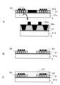
工程(b)は、配線基板2の上面に、凹部34を有する下部クラッド31を形成する工程である。図8Aに示すように、下部クラッド31の材料となる樹脂フィルム31aを、配線基板2の上面(金属層21aの上面)に載置する。樹脂フィルム31aとしては、上記の下部クラッド31で説明したように、例えば、エポキシ樹脂およびシリコン樹脂などの樹脂で形成されたフィルムが挙げられる。樹脂フィルム31aは、得られる下部クラッド31の厚みを考慮して、例えば5μm以上200μm以下の厚みを有する。図8Aでは金属層21aが形成されているものの、金属層21aは無くても差し支えない。
Step (b) is a step of forming a lower clad 31 having a recess 34 on the upper surface of the wiring board 2. As shown in FIG. 8A, a resin film 31a, which is the material of the lower clad 31, is placed on the upper surface of the wiring board 2 (the upper surface of the metal layer 21a). As described above for the lower clad 31, examples of the resin film 31a include films formed from resins such as epoxy resin and silicone resin. The resin film 31a has a thickness of, for example, 5 μm or more and 200 μm or less, taking into account the thickness of the resulting lower clad 31. Although the metal layer 21a is formed in FIG. 8A, the metal layer 21a is not necessary.
次いで、図8Bに示すように、樹脂フィルム31aをモールド35で被覆する。モールド35には、露光時にマスクとして作用する遮光部35aが形成されている。遮光部35aは、例えばクロムなどの金属や樹脂で形成されている。樹脂フィルム31aをモールド35で被覆した後、露光および現像し、図8Cに示すように、下部クラッド31に凹部34が形成される。具体的には、遮光部35aで遮蔽された部分は硬化せず、現像で除去されることで凹部34が形成される。
Then, as shown in FIG. 8B, the resin film 31a is covered with a mold 35. The mold 35 is formed with a light-shielding portion 35a that acts as a mask during exposure. The light-shielding portion 35a is formed of a metal such as chromium or a resin. After the resin film 31a is covered with the mold 35, it is exposed to light and developed, and as shown in FIG. 8C, a recess 34 is formed in the lower clad 31. Specifically, the portion shielded by the light-shielding portion 35a does not harden and is removed by development to form the recess 34.
工程(c)は、下部クラッド31の上面にコア用樹脂32aを被着する工程である。図9Aに示すように、下部クラッド31を被覆するように、コア用樹脂32aを被着する。コア用樹脂32aとしては、上記のコア32で説明したように、例えば、エポキシ樹脂およびシリコン樹脂などの樹脂で形成されたフィルムが挙げられる。コア用樹脂32aは、得られるコア32の厚みを考慮して、例えば1μm以上65μm以下の厚みを有する。
Step (c) is a step of applying core resin 32a to the upper surface of lower clad 31. As shown in FIG. 9A, core resin 32a is applied so as to cover lower clad 31. As described above for core 32, examples of core resin 32a include films formed of resins such as epoxy resin and silicone resin. Taking into account the thickness of the resulting core 32, core resin 32a has a thickness of, for example, 1 μm or more and 65 μm or less.
工程(d)は、第1面361および第1面361と反対側に第2面362を有し、第1面361にコアパターン用溝363およびコアパターン用溝363以外の部分に遮光部364を有する光透過性のモールド36を準備する工程である。図9Bに示すように、コアパターン用溝363は、モールド36の第1面361に、所望のコア32に幅、高さおよび形状を考慮して形成されている。遮光部364は、コアパターン用溝363以外の部分に位置しており、例えばクロムなどの金属で形成されている。
Step (d) is a step of preparing a light-transmitting mold 36 having a first surface 361 and a second surface 362 opposite the first surface 361, and having a core pattern groove 363 on the first surface 361 and a light-shielding portion 364 in a portion other than the core pattern groove 363. As shown in FIG. 9B, the core pattern groove 363 is formed on the first surface 361 of the mold 36, taking into consideration the width, height and shape of the desired core 32. The light-shielding portion 364 is located in a portion other than the core pattern groove 363, and is formed of a metal such as chromium.
工程(e)は、平面透視で、コアパターン用溝363が凹部34と重ならずに沿うように、コア用樹脂32a上に第1面361が接触するように、モールド36を載置する工程である。モールド36を載置した後、工程(f)によってモールド36を押圧する。
In step (e), the mold 36 is placed so that the first surface 361 is in contact with the core resin 32a and so that the core pattern grooves 363 are aligned with but do not overlap the recesses 34 in a plan view. After the mold 36 is placed, the mold 36 is pressed in step (f).
工程(f)は、コアパターン用溝363および凹部34に、コア用樹脂32aが位置するように、コア用樹脂32a上に載置されたモールド36を押圧する工程である。図9Cに示すように、モールド36を押圧することによって、コア用樹脂32aの一部が凹部34に流れ込む。すなわち、余分なコア用樹脂32aが凹部34に流れ込むことによって、得られるコア32の厚みのバラツキを低減することができる。その結果、光信号の伝送損失を低減することができる。凹部34に流れ込んだコア用樹脂32aは凹みを有していてもよい。
Step (f) is a step of pressing the mold 36 placed on the core resin 32a so that the core resin 32a is positioned in the core pattern groove 363 and the recess 34. As shown in FIG. 9C, pressing the mold 36 causes a portion of the core resin 32a to flow into the recess 34. In other words, by having excess core resin 32a flow into the recess 34, it is possible to reduce variation in the thickness of the resulting core 32. As a result, it is possible to reduce the transmission loss of the optical signal. The core resin 32a that has flowed into the recess 34 may have a recess.
さらに、凹部34がコア32を間に挟むように位置していると、モールド36を押圧した際に、余分なコア用樹脂32aが分散して各凹部34に流れ込む。その結果、得られるコア32の厚みのバラツキを、より効率よく低減することができる。
Furthermore, if the recesses 34 are positioned so as to sandwich the core 32, when the mold 36 is pressed, the excess core resin 32a disperses and flows into each recess 34. As a result, the variation in thickness of the resulting core 32 can be reduced more efficiently.
上述のように、下部クラッド31において、凹部34の占める割合は限定されない。例えば、凹部34の総容積は、コア32の総体積よりも大きくてもよい。凹部34の総容積が大きいと、余分なコア用樹脂32aが凹部34に流れ込みやすくなる。その結果、得られるコア32の厚みのバラツキを、より効率よく低減することができる。
As described above, the proportion of the recesses 34 in the lower cladding 31 is not limited. For example, the total volume of the recesses 34 may be larger than the total volume of the core 32. If the total volume of the recesses 34 is large, excess core resin 32a tends to flow into the recesses 34. As a result, the variation in thickness of the resulting core 32 can be reduced more efficiently.
工程(g)は、モールド36の第2面362側から露光し、コアパターン用溝363およびコアパターン用溝363の下部に位置するコア用樹脂32aを半硬化させる工程である。図9Cに示すように、露光は、例えば紫外線(UV)を照射することによって行われる。コア用樹脂32aを半硬化させるための紫外線量(強さ)や露光時間は、使用するコア用樹脂32aの種類によって適宜設定される。遮光部364で被覆されているコア用樹脂32aは半硬化されずに、未硬化のままである。
Step (g) is a step of exposing the second surface 362 of the mold 36 to light to semi-cure the core pattern groove 363 and the core resin 32a located below the core pattern groove 363. As shown in FIG. 9C, the exposure is performed by, for example, irradiating ultraviolet (UV) light. The amount (strength) of ultraviolet light and the exposure time for semi-cure the core resin 32a are appropriately set depending on the type of core resin 32a used. The core resin 32a covered by the light-shielding portion 364 is not semi-cure and remains uncured.
図10Aに示すように、凹部34の幅は、底部から開口部に向かって広くなっていてもよい。凹部34の幅が底部から開口部に向かって広くなっていると、余分なコア用樹脂32aが凹部34に流れ込みやすくなる。その結果、得られるコア32の厚みのバラツキを、より効率よく低減することができる。
As shown in FIG. 10A, the width of the recess 34 may increase from the bottom toward the opening. If the width of the recess 34 increases from the bottom toward the opening, excess core resin 32a will flow into the recess 34 more easily. As a result, the variation in thickness of the resulting core 32 can be reduced more efficiently.
工程(h)は、モールド36を除去し、下部クラッド31の上面および凹部34に位置する未硬化のコア用樹脂32aを現像し除去した後、コア用樹脂32aを硬化させることによって、コア32を形成する工程である。図10Aに示すようにモールド36を除去した後、図10Bに示すように、遮光部364で被覆されていた部分の未硬化のコア用樹脂32aを現像して除去する。
In step (h), the mold 36 is removed, the uncured core resin 32a located on the upper surface and in the recess 34 of the lower cladding 31 is developed and removed, and then the core resin 32a is cured to form the core 32. After removing the mold 36 as shown in FIG. 10A, the uncured core resin 32a in the portion covered by the light shielding portion 364 is developed and removed as shown in FIG. 10B.
遮光部364で被覆されていた部分のコア用樹脂32aを除去した後、残った半硬化状態のコア用樹脂32a(遮光部364で被覆されていない部分のコア用樹脂32a)を、硬化させる。硬化は、例えば紫外線を照射することによって行われる。このようにして、図10Bに示すように、下部クラッド31の上面にコア32が、各々の厚みバラツキが低減された状態で形成される。
After removing the core resin 32a from the portion that was covered by the light-shielding portion 364, the remaining semi-cured core resin 32a (the portion of the core resin 32a that is not covered by the light-shielding portion 364) is cured. The curing is performed, for example, by irradiating it with ultraviolet light. In this way, as shown in FIG. 10B, the cores 32 are formed on the upper surface of the lower cladding 31 with reduced variation in thickness.
工程(i)は、下部クラッド31の上面およびコア32を被覆し、凹部34に位置する上部クラッド33を形成する工程である。上部クラッド33を形成する方法の一例として、まず、上部クラッド33の材料となる樹脂フィルムを準備する。樹脂フィルムとしては、上記の上部クラッド33で説明したように、例えば、エポキシ樹脂およびシリコン樹脂などの樹脂で形成されたフィルムが挙げられる。樹脂フィルムは、得られる上部クラッド33の厚みを考慮して、例えば5μm以上250μm以下の厚みを有する。
Step (i) is a step of forming the upper clad 33, which covers the upper surface of the lower clad 31 and the core 32 and is located in the recess 34. As an example of a method of forming the upper clad 33, first, a resin film that will be the material for the upper clad 33 is prepared. As described above for the upper clad 33, examples of the resin film include films formed from resins such as epoxy resin and silicone resin. Taking into account the thickness of the resulting upper clad 33, the resin film has a thickness of, for example, 5 μm or more and 250 μm or less.
次いで、上部クラッド33の材料となる樹脂フィルムを、図10Bに示す下部クラッド31の上面およびコア32の上面に載置する。その後、樹脂フィルムを加熱および加圧して、下部クラッド31の上面およびコア32を被覆し、樹脂フィルムの一部が凹部34に位置するように積層し、図10Cに示すような上部クラッド33を形成する。
Next, a resin film that will be the material for the upper clad 33 is placed on the top surface of the lower clad 31 and the top surface of the core 32 shown in FIG. 10B. The resin film is then heated and pressurized to cover the top surface of the lower clad 31 and the core 32, and is laminated so that a portion of the resin film is positioned in the recess 34, forming the upper clad 33 as shown in FIG. 10C.
このような工程(a)~(i)によって、コアの厚みのバラツキを小さくすることができ、光信号の伝送損失が少なく、かつ上部クラッドと下部クラッドとの密着力に優れた一実施形態に係る光回路基板1が得られる。
By carrying out steps (a) to (i) in this way, it is possible to obtain an optical circuit board 1 according to one embodiment that has a small variation in the thickness of the core, a small transmission loss of the optical signal, and excellent adhesion between the upper clad and the lower clad.
次に、本開示の光学部品実装構造体について説明する。本開示の一実施形態に係る光学部品実装構造体10は、図1に示すように、一実施形態に係る光回路基板1に光学部品4および電子部品6が実装された構造を有している。一実施形態に係る光学部品実装構造体10に実装される光学部品4には、光伝送路41が含まれる。このような光伝送路41を含む光学部品4としては、例えば、シリコンフォトニクスデバイスなどが挙げられる。電子部品6としては、例えば、ASIC(Application Specific Integrated Circuit)、ドライバICなどが挙げられる。
Next, the optical component mounting structure of the present disclosure will be described. As shown in FIG. 1, an optical component mounting structure 10 according to an embodiment of the present disclosure has a structure in which an optical component 4 and an electronic component 6 are mounted on an optical circuit board 1 according to an embodiment. The optical component 4 mounted on the optical component mounting structure 10 according to an embodiment includes an optical transmission path 41. Examples of optical components 4 including such optical transmission paths 41 include silicon photonics devices. Examples of electronic components 6 include ASICs (Application Specific Integrated Circuits) and driver ICs.
図2に示すように、光学部品4は、配線基板2と電気的に接続されている。具体的には、光学部品4は、配線基板2の実装領域(光学部品の実装領域)に位置するパッド21bとはんだ7を介して電気的に接続されている。パッド21bは、配線基板2の上面に位置する導体層の一部である。
As shown in FIG. 2, the optical component 4 is electrically connected to the wiring board 2. Specifically, the optical component 4 is electrically connected to a pad 21b located in the mounting area (optical component mounting area) of the wiring board 2 via solder 7. The pad 21b is part of a conductor layer located on the upper surface of the wiring board 2.
光学部品4の一例として、シリコンフォトニクスデバイスについて説明する。シリコンフォトニクスデバイスは、例えば、ケイ素(Si)をコアとし、二酸化ケイ素(SiO2)をクラッドとする光伝送路41を有する光学部品の1種である。シリコンフォトニクスデバイスは、光伝送路41としてSi導波路を含み、図示していないが、パッシベーション膜、光源部および光検出部などをさらに含んでいる。上述のように、光伝送路41(Si導波路41)は、光導波路3の一方の端部において、光導波路3に含まれるコア32と対向するように位置している。
A silicon photonics device will be described as an example of the optical component 4. The silicon photonics device is a type of optical component having an optical transmission path 41 with, for example, silicon (Si) as a core and silicon dioxide (SiO 2 ) as a cladding. The silicon photonics device includes a Si waveguide as the optical transmission path 41, and further includes a passivation film, a light source unit, a light detection unit, and the like, although not shown. As described above, the optical transmission path 41 (Si waveguide 41) is located at one end of the optical waveguide 3 so as to face the core 32 included in the optical waveguide 3.
例えば、配線基板2からの電気信号が、はんだ7を介して光学部品4(シリコンフォトニクスデバイス)に含まれる光源部に伝搬される。伝搬された電気信号を受信した光源部は発光する。発光した光信号が光伝送路41(Si導波路41)およびコア32を経由して、光コネクター5aを介して接続されている光ファイバー5に伝播される。
For example, an electrical signal from the wiring board 2 is transmitted via the solder 7 to the light source section included in the optical component 4 (silicon photonics device). The light source section receives the transmitted electrical signal and emits light. The emitted optical signal is transmitted via the optical transmission path 41 (Si waveguide 41) and the core 32 to the optical fiber 5 connected via the optical connector 5a.
さらに、本開示に係る発明は上述の実施形態に限定されるものではなく、下記の(1)、(11)および(12)に示す本開示の範囲内で種々の変更および改良が可能である。
Furthermore, the invention disclosed herein is not limited to the above-described embodiments, and various modifications and improvements are possible within the scope of the present disclosure as shown in (1), (11), and (12) below.
(1)本開示に係る光回路基板は、配線基板と配線基板上に位置する光導波路とを含む。光導波路は、配線基板の上面側から下部クラッド、コアおよび上部クラッドを含む。コアは、下部クラッドの上面に延在している。上部クラッドは、下部クラッドの上面およびコアを被覆している。下部クラッドは、コアに沿って位置する少なくとも1つの凹部を有している。上部クラッドの一部は、凹部に位置している。
(1) The optical circuit board according to the present disclosure includes a wiring board and an optical waveguide located on the wiring board. The optical waveguide includes a lower cladding, a core, and an upper cladding from the upper surface side of the wiring board. The core extends to the upper surface of the lower cladding. The upper cladding covers the upper surface of the lower cladding and the core. The lower cladding has at least one recess located along the core. A portion of the upper cladding is located in the recess.
本開示の実施形態に関し、以下の(2)~(10)に示す実施形態をさらに開示する。
The following embodiments (2) to (10) are further disclosed with respect to the embodiments of the present disclosure.
(2)上記(1)に記載の光回路基板において、凹部は、コアを間に挟むように位置する第1凹部と第2凹部とを有している。
(3)上記(2)に記載の光回路基板において、コアは、互いに隣接して複数位置している。
(4)上記(1)に記載の光回路基板において、コアは、互いに隣接して複数位置しており、複数のコア各々を間に挟むように凹部が複数位置している。
(5)上記(1)~(4)のいずれかに記載の光回路基板において、凹部は、底部と開口部とを有している。コアが延在する方向と垂直な方向の断面視において、凹部の開口部の幅は、凹部の底部の幅よりも大きい。
(6)上記(5)に記載の光回路基板において、凹部の幅は、底部から開口部に向かって広くなっている。
(7)上記(1)~(6)のいずれかに記載の光回路基板において、凹部の内壁面の算術平均粗さは、下部クラッドの上面の算術平均粗さよりも大きい。
(8)上記(1)~(7)のいずれかに記載の光回路基板において、配線基板は金属層をさらに含み、光導波路は金属層の上面に位置している。
(9)上記(8)のいずれかに記載の光回路基板において、凹部は下部クラッドの上面から金属層にわたって位置しており、上部クラッドが金属層に接している。
(10)上記(1)~(9)のいずれかに記載の光回路基板において、上部クラッドは、平面透視で、凹部と重なる領域に窪みを有する。 (2) In the optical circuit board described in (1) above, the recess has a first recess and a second recess positioned to sandwich the core therebetween.
(3) In the optical circuit board described in (2) above, a plurality of cores are positioned adjacent to each other.
(4) In the optical circuit board described in (1) above, a plurality of cores are positioned adjacent to each other, and a plurality of recesses are positioned so as to sandwich each of the plurality of cores therebetween.
(5) In the optical circuit board according to any one of (1) to (4) above, the recess has a bottom and an opening, and in a cross-sectional view perpendicular to the direction in which the core extends, the width of the opening of the recess is greater than the width of the bottom of the recess.
(6) In the optical circuit board according to (5) above, the width of the recess increases from the bottom toward the opening.
(7) In the optical circuit board according to any one of (1) to (6) above, the arithmetic mean roughness of the inner wall surface of the recess is greater than the arithmetic mean roughness of the upper surface of the lower cladding.
(8) In the optical circuit board according to any one of (1) to (7) above, the wiring board further includes a metal layer, and the optical waveguide is located on an upper surface of the metal layer.
(9) In the optical circuit board according to any one of (8) above, the recess is located from the upper surface of the lower clad to the metal layer, and the upper clad is in contact with the metal layer.
(10) In the optical circuit board according to any one of (1) to (9) above, the upper clad has a depression in a region overlapping with the recess in a plan view.
(11)本開示に係る光学部品実装構造体は、上記(1)~(10)のいずれかに記載の光回路基板と光回路基板に実装された光学部品とを含む。
(11) The optical component mounting structure according to the present disclosure includes an optical circuit board described in any one of (1) to (10) above and an optical component mounted on the optical circuit board.
(12)本開示に係る光回路基板の製造方法は、配線基板を準備する工程と、配線基板の上面に、凹部を有する下部クラッドを形成する工程と、下部クラッドの上面にコア用樹脂を被着する工程と、第1面および第1面と反対側に第2面を有し、第1面にコアパターン用溝と、コアパターン用溝以外の部分に遮光部とを有する光透過性のモールドを準備する工程と、平面透視で、コアパターン用溝が凹部と重ならずに沿うように、コア用樹脂上に第1面が接触するように、モールドを載置する工程と、コアパターン用溝および凹部に、コア用樹脂が位置するように、コア用樹脂上に載置されたモールドを押圧する工程と、モールドの第2面側から露光し、コアパターン用溝およびコアパターン用溝の下部に位置するコア用樹脂を半硬化させる工程と、モールドを除去し、下部クラッドの上面および凹部に位置する未硬化のコア用樹脂を現像し除去した後、コア用樹脂を硬化させることによって、コアを形成する工程と、下部クラッドの上面およびコアを被覆し、凹部に位置する上部クラッドを形成する工程とを含む。
(12) A method for manufacturing an optical circuit board according to the present disclosure includes the steps of preparing a wiring board, forming a lower clad having a recess on the upper surface of the wiring board, applying a core resin to the upper surface of the lower clad, preparing a light-transmitting mold having a first surface and a second surface opposite the first surface, a core pattern groove on the first surface, and a light-shielding portion in a portion other than the core pattern groove, placing the mold so that the first surface is in contact with the core resin and so that the core pattern groove is aligned with the recess without overlapping it in a planar perspective view, and The process includes a step of pressing a mold placed on the core resin so that the core resin is positioned in the turn groove and the recess; a step of exposing the mold from the second surface side to semi-cure the core resin located in the core pattern groove and the lower part of the core pattern groove; a step of removing the mold, developing and removing the uncured core resin located on the upper surface of the lower clad and in the recess, and then curing the core resin to form a core; and a step of covering the upper surface of the lower clad and the core to form an upper clad located in the recess.
(13)上記(12)に記載の製造方法において、配線基板は金属層をさらに含み、下部クラッドを金属層上に形成する。
(13) In the manufacturing method described in (12) above, the wiring substrate further includes a metal layer, and a lower clad is formed on the metal layer.
1 光回路基板
2 配線基板
21a 金属層
21b パッド
3 光導波路
31 下部クラッド
32 コア
33 上部クラッド
331 窪み
34 凹部
35 モールド
35a 遮光部
36 モールド
361 第1面
362 第2面
363 コアパターン用溝
364 遮光部
4 光学部品
41 光伝送路(シリコン導波路(Si導波路))
5 光ファイバー
5a 光コネクター
6 電子部品
7 はんだ
10 光学部品実装構造体 REFERENCE SIGNSLIST 1 Optical circuit board 2 Wiring board 21a Metal layer 21b Pad 3 Optical waveguide 31 Lower clad 32 Core 33 Upper clad 331 Recess 34 Concave portion 35 Mold 35a Light shielding portion 36 Mold 361 First surface 362 Second surface 363 Groove for core pattern 364 Light shielding portion 4 Optical component 41 Optical transmission path (silicon waveguide (Si waveguide))
5Optical fiber 5a Optical connector 6 Electronic component 7 Solder 10 Optical component mounting structure
2 配線基板
21a 金属層
21b パッド
3 光導波路
31 下部クラッド
32 コア
33 上部クラッド
331 窪み
34 凹部
35 モールド
35a 遮光部
36 モールド
361 第1面
362 第2面
363 コアパターン用溝
364 遮光部
4 光学部品
41 光伝送路(シリコン導波路(Si導波路))
5 光ファイバー
5a 光コネクター
6 電子部品
7 はんだ
10 光学部品実装構造体 REFERENCE SIGNS
5
Claims (13)
- 配線基板と、
該配線基板上に位置する光導波路と、
を含み、
該光導波路は、前記配線基板の上面側から下部クラッド、コアおよび上部クラッドを含み、
前記コアは、前記下部クラッドの上面に延在しており、
前記上部クラッドは、前記下部クラッドの上面および前記コアを被覆しており、
前記下部クラッドは、前記コアに沿って位置する少なくとも1つの凹部を有し、
前記上部クラッドの一部が、前記凹部に位置している、
光回路基板。 A wiring board;
an optical waveguide located on the wiring substrate;
Including,
the optical waveguide includes, from the upper surface side of the wiring board, a lower clad, a core, and an upper clad;
the core extends over an upper surface of the lower cladding;
the upper clad covers an upper surface of the lower clad and the core,
the lower cladding has at least one recess located along the core;
A portion of the upper cladding is located in the recess.
Optical circuit board. - 前記凹部は、前記コアを間に挟むように位置する第1凹部と第2凹部とを有している、請求項1に記載の光回路基板。 The optical circuit board according to claim 1, wherein the recess has a first recess and a second recess positioned so as to sandwich the core therebetween.
- 前記コアは、互いに隣接して複数位置している、請求項2に記載の光回路基板。 The optical circuit board according to claim 2, wherein the cores are positioned adjacent to each other.
- 前記コアは、互いに隣接して複数位置しており、該複数の前記コア各々を間に挟むように前記凹部が複数位置している、請求項1に記載の光回路基板。 The optical circuit board according to claim 1, wherein the cores are positioned adjacent to each other, and the recesses are positioned so as to sandwich each of the cores.
- 前記凹部は、底部と開口部とを有しており、
前記コアが延在する方向と垂直な方向の断面視において、前記凹部の前記開口部の幅は、前記凹部の前記底部の幅よりも大きい、請求項1~4のいずれかに記載の光回路基板。 The recess has a bottom and an opening,
5. The optical circuit board according to claim 1, wherein, in a cross-sectional view perpendicular to the extending direction of the core, a width of the opening of the recess is larger than a width of the bottom of the recess. - 前記凹部の幅は、前記底部から前記開口部に向かって広くなっている、請求項5に記載の光回路基板。 The optical circuit board according to claim 5, wherein the width of the recess increases from the bottom toward the opening.
- 前記凹部の内壁面の算術平均粗さは、前記下部クラッドの上面の算術平均粗さよりも大きい、請求項1~6のいずれかに記載の光回路基板。 An optical circuit board according to any one of claims 1 to 6, in which the arithmetic mean roughness of the inner wall surface of the recess is greater than the arithmetic mean roughness of the upper surface of the lower cladding.
- 前記配線基板は、金属層をさらに含み、前記光導波路は前記金属層の上面に位置している、請求項1~7のいずれかに記載の光回路基板。 The optical circuit board according to any one of claims 1 to 7, wherein the wiring board further includes a metal layer, and the optical waveguide is located on the upper surface of the metal layer.
- 前記凹部は、前記下部クラッドの上面から前記金属層にわたって位置しており、前記上部クラッドが前記金属層に接している、請求項8に記載の光回路基板。 The optical circuit board according to claim 8, wherein the recess is located from the upper surface of the lower cladding to the metal layer, and the upper cladding is in contact with the metal layer.
- 前記上部クラッドは、平面透視で、前記凹部と重なる領域に窪みを有する、請求項1~9のいずれかに記載の光回路基板。 The optical circuit board according to any one of claims 1 to 9, wherein the upper cladding has a depression in an area that overlaps with the recess in plan view.
- 請求項1~10のいずれかに記載の光回路基板と、
該光回路基板に実装された光学部品と
を含む、光学部品実装構造体。 An optical circuit board according to any one of claims 1 to 10,
and an optical component mounted on the optical circuit board. - 配線基板を準備する工程と、
該配線基板の上面に、凹部を有する下部クラッドを形成する工程と、
該下部クラッドの上面にコア用樹脂を被着する工程と、
第1面および該第1面と反対側に第2面を有し、前記第1面にコアパターン用溝と、該コアパターン用溝以外の部分に遮光部とを有する光透過性のモールドを準備する工程と、
平面透視で、前記コアパターン用溝が前記凹部と重ならずに沿うように、前記コア用樹脂上に前記第1面が接触するように、前記モールドを載置する工程と、
前記コアパターン用溝および前記凹部に、前記コア用樹脂が位置するように、前記コア用樹脂上に載置された前記モールドを押圧する工程と、
前記モールドの前記第2面側から露光し、前記コアパターン用溝および前記コアパターン用溝の下部に位置する前記コア用樹脂を半硬化させる工程と、
前記モールドを除去し、前記下部クラッドの上面および前記凹部に位置する未硬化の前記コア用樹脂を現像し除去した後、前記コア用樹脂を硬化させることによって、コアを形成する工程と、
前記下部クラッドの上面および前記コアを被覆し、前記凹部に位置する上部クラッドを形成する工程と、
を含む、光回路基板の製造方法。 preparing a wiring board;
forming a lower clad having a recess on an upper surface of the wiring substrate;
applying a core resin to an upper surface of the lower clad;
A step of preparing a light-transmitting mold having a first surface and a second surface opposite to the first surface, the mold having a groove for a core pattern on the first surface and a light-shielding portion in a portion other than the groove for the core pattern;
placing the mold so that the first surface is in contact with the core resin such that the core pattern groove is aligned with the recess without overlapping with the recess in a plan view perspective;
pressing the mold placed on the core resin so that the core resin is positioned in the core pattern groove and the recess;
a step of exposing the mold from the second surface side to light to semi-cure the core resin located in the core pattern groove and below the core pattern groove;
removing the mold, developing and removing the uncured core resin located on the upper surface of the lower clad and in the recess, and then curing the core resin to form a core;
forming an upper clad covering an upper surface of the lower clad and the core and located in the recess;
A method for manufacturing an optical circuit board, comprising: - 前記配線基板は、金属層をさらに含み、前記下部クラッドを前記金属層上に形成する、請求項12に記載の光回路基板の製造方法。 The method for manufacturing an optical circuit board according to claim 12, wherein the wiring board further includes a metal layer, and the lower clad is formed on the metal layer.
Applications Claiming Priority (2)
| Application Number | Priority Date | Filing Date | Title |
|---|---|---|---|
| JP2022-191274 | 2022-11-30 | ||
| JP2022191274 | 2022-11-30 |
Publications (1)
| Publication Number | Publication Date |
|---|---|
| WO2024117023A1 true WO2024117023A1 (en) | 2024-06-06 |
Family
ID=91323994
Family Applications (1)
| Application Number | Title | Priority Date | Filing Date |
|---|---|---|---|
| PCT/JP2023/042123 WO2024117023A1 (en) | 2022-11-30 | 2023-11-24 | Optical circuit board, optical component mounting structure, and method for manufacturing optical circuit board |
Country Status (1)
| Country | Link |
|---|---|
| WO (1) | WO2024117023A1 (en) |
Citations (8)
| Publication number | Priority date | Publication date | Assignee | Title |
|---|---|---|---|---|
| JPH01198706A (en) * | 1987-12-02 | 1989-08-10 | Furukawa Electric Co Ltd:The | Embedded type optical waveguide |
| JP2004233406A (en) * | 2003-01-28 | 2004-08-19 | Fuji Xerox Co Ltd | Manufacturing method of optical waveguide substrate, optical waveguide substrate, and light reflecting structure body |
| JP2004295118A (en) * | 2003-03-12 | 2004-10-21 | Sanyo Electric Co Ltd | Optical waveguide |
| JP2008262003A (en) * | 2007-04-11 | 2008-10-30 | Sumitomo Electric Ind Ltd | Optical waveguide and method of manufacturing the same |
| JP2011007886A (en) * | 2009-06-23 | 2011-01-13 | Nippon Shokubai Co Ltd | Method of manufacturing optical waveguide and die used for the same |
| US20150003778A1 (en) * | 2011-12-08 | 2015-01-01 | Lg Innotek Co., Ltd. | Optical printed circuit board and method of manufacturing the same |
| US20150192735A1 (en) * | 2014-01-09 | 2015-07-09 | International Business Machines Corporation | Shielding structures between optical waveguides |
| JP2019082576A (en) * | 2017-10-31 | 2019-05-30 | 日本電信電話株式会社 | Optical waveguide and manufacturing method of the same |
-
2023
- 2023-11-24 WO PCT/JP2023/042123 patent/WO2024117023A1/en unknown
Patent Citations (8)
| Publication number | Priority date | Publication date | Assignee | Title |
|---|---|---|---|---|
| JPH01198706A (en) * | 1987-12-02 | 1989-08-10 | Furukawa Electric Co Ltd:The | Embedded type optical waveguide |
| JP2004233406A (en) * | 2003-01-28 | 2004-08-19 | Fuji Xerox Co Ltd | Manufacturing method of optical waveguide substrate, optical waveguide substrate, and light reflecting structure body |
| JP2004295118A (en) * | 2003-03-12 | 2004-10-21 | Sanyo Electric Co Ltd | Optical waveguide |
| JP2008262003A (en) * | 2007-04-11 | 2008-10-30 | Sumitomo Electric Ind Ltd | Optical waveguide and method of manufacturing the same |
| JP2011007886A (en) * | 2009-06-23 | 2011-01-13 | Nippon Shokubai Co Ltd | Method of manufacturing optical waveguide and die used for the same |
| US20150003778A1 (en) * | 2011-12-08 | 2015-01-01 | Lg Innotek Co., Ltd. | Optical printed circuit board and method of manufacturing the same |
| US20150192735A1 (en) * | 2014-01-09 | 2015-07-09 | International Business Machines Corporation | Shielding structures between optical waveguides |
| JP2019082576A (en) * | 2017-10-31 | 2019-05-30 | 日本電信電話株式会社 | Optical waveguide and manufacturing method of the same |
Similar Documents
| Publication | Publication Date | Title |
|---|---|---|
| US8548285B2 (en) | Manufacturing method of optical sensor module and optical sensor module obtained thereby | |
| US8989529B2 (en) | Printed circuit board for optical waveguides and method of manufacturing same | |
| JP2009175418A (en) | Opto-electronic printed wiring board and manufacturing method of same | |
| JP2005275405A (en) | Optical structure and method for connecting optical circuit board components | |
| JP2008139465A (en) | Method of manufacturing optoelectric hybrid board | |
| KR20100066155A (en) | Printed circuit board for optical waveguides and method of manufacturing the same | |
| US7801399B2 (en) | Method of forming optical waveguide | |
| JP2009103827A (en) | Photoelectric complex substrate, and manufacturing method therefor | |
| WO2024117023A1 (en) | Optical circuit board, optical component mounting structure, and method for manufacturing optical circuit board | |
| JP5230324B2 (en) | OPTICAL TRANSMISSION BOARD, OPTICAL MODULE, AND OPTICAL TRANSMISSION BOARD MANUFACTURING METHOD | |
| WO2022210230A1 (en) | Optical circuit board and optical component mounting structure using same | |
| TW202430946A (en) | Optical circuit substrate, optical component mounted structure, and method of manufacturing optical circuit substrate | |
| WO2023038132A1 (en) | Optical circuit board and optical component mounting structure using same | |
| WO2022163481A1 (en) | Optical circuit board and electronic component mounting structure using same | |
| WO2023145593A1 (en) | Optical circuit board | |
| WO2023190186A1 (en) | Optical circuit board | |
| WO2024143134A1 (en) | Optical circuit board, optical component mounting structure, and method for producing optical circuit board | |
| WO2022091914A1 (en) | Optical circuit board and electronic component mounting structure using same | |
| JP2002022976A (en) | Optical/electronic printed circuit board and method for manufacturing the same | |
| TW202409535A (en) | Optical circuit board and optical component mounting structure | |
| WO2023162964A1 (en) | Optical circuit board | |
| JP7520983B2 (en) | Optical Circuit Board | |
| JP2003014946A (en) | Photoelectron printing circuit board and method for manufacturing the same | |
| WO2023095768A1 (en) | Optical circuit board | |
| WO2024075496A1 (en) | Optical waveguide |
Legal Events
| Date | Code | Title | Description |
|---|---|---|---|
| 121 | Ep: the epo has been informed by wipo that ep was designated in this application |
Ref document number: 23897671 Country of ref document: EP Kind code of ref document: A1 |