WO2024101296A1 - 樹脂組成物、硬化物、積層体、硬化物の製造方法、積層体の製造方法、半導体デバイスの製造方法、及び、半導体デバイス - Google Patents
樹脂組成物、硬化物、積層体、硬化物の製造方法、積層体の製造方法、半導体デバイスの製造方法、及び、半導体デバイス Download PDFInfo
- Publication number
- WO2024101296A1 WO2024101296A1 PCT/JP2023/039836 JP2023039836W WO2024101296A1 WO 2024101296 A1 WO2024101296 A1 WO 2024101296A1 JP 2023039836 W JP2023039836 W JP 2023039836W WO 2024101296 A1 WO2024101296 A1 WO 2024101296A1
- Authority
- WO
- WIPO (PCT)
- Prior art keywords
- filler
- resin composition
- group
- polyimide
- cured product
- Prior art date
- Legal status (The legal status is an assumption and is not a legal conclusion. Google has not performed a legal analysis and makes no representation as to the accuracy of the status listed.)
- Ceased
Links
Classifications
-
- B—PERFORMING OPERATIONS; TRANSPORTING
- B32—LAYERED PRODUCTS
- B32B—LAYERED PRODUCTS, i.e. PRODUCTS BUILT-UP OF STRATA OF FLAT OR NON-FLAT, e.g. CELLULAR OR HONEYCOMB, FORM
- B32B27/00—Layered products comprising a layer of synthetic resin
- B32B27/18—Layered products comprising a layer of synthetic resin characterised by the use of special additives
- B32B27/20—Layered products comprising a layer of synthetic resin characterised by the use of special additives using fillers, pigments, thixotroping agents
-
- B—PERFORMING OPERATIONS; TRANSPORTING
- B32—LAYERED PRODUCTS
- B32B—LAYERED PRODUCTS, i.e. PRODUCTS BUILT-UP OF STRATA OF FLAT OR NON-FLAT, e.g. CELLULAR OR HONEYCOMB, FORM
- B32B27/00—Layered products comprising a layer of synthetic resin
- B32B27/34—Layered products comprising a layer of synthetic resin comprising polyamides
-
- C—CHEMISTRY; METALLURGY
- C08—ORGANIC MACROMOLECULAR COMPOUNDS; THEIR PREPARATION OR CHEMICAL WORKING-UP; COMPOSITIONS BASED THEREON
- C08K—Use of inorganic or non-macromolecular organic substances as compounding ingredients
- C08K3/00—Use of inorganic substances as compounding ingredients
- C08K3/01—Use of inorganic substances as compounding ingredients characterized by their specific function
- C08K3/013—Fillers, pigments or reinforcing additives
-
- C—CHEMISTRY; METALLURGY
- C08—ORGANIC MACROMOLECULAR COMPOUNDS; THEIR PREPARATION OR CHEMICAL WORKING-UP; COMPOSITIONS BASED THEREON
- C08L—COMPOSITIONS OF MACROMOLECULAR COMPOUNDS
- C08L79/00—Compositions of macromolecular compounds obtained by reactions forming in the main chain of the macromolecule a linkage containing nitrogen with or without oxygen or carbon only, not provided for in groups C08L61/00 - C08L77/00
- C08L79/04—Polycondensates having nitrogen-containing heterocyclic rings in the main chain; Polyhydrazides; Polyamide acids or similar polyimide precursors
- C08L79/08—Polyimides; Polyester-imides; Polyamide-imides; Polyamide acids or similar polyimide precursors
-
- H—ELECTRICITY
- H05—ELECTRIC TECHNIQUES NOT OTHERWISE PROVIDED FOR
- H05K—PRINTED CIRCUITS; CASINGS OR CONSTRUCTIONAL DETAILS OF ELECTRIC APPARATUS; MANUFACTURE OF ASSEMBLAGES OF ELECTRICAL COMPONENTS
- H05K1/00—Printed circuits
- H05K1/02—Details
- H05K1/03—Use of materials for the substrate
Definitions
- the present invention relates to a resin composition, a cured product, a laminate, a method for producing a cured product, a method for producing a laminate, a method for producing a semiconductor device, and a semiconductor device.
- resin materials produced from resin compositions containing resins are being used in various fields.
- polyimide is used in various applications due to its excellent heat resistance and insulating properties.
- the applications include, but are not limited to, materials for insulating films and sealing materials, or protective films for semiconductor devices for mounting.
- Polyimide is also used as a base film or coverlay for flexible substrates.
- polyimide is used in the form of a resin composition containing a polyimide precursor.
- a resin composition is applied to a substrate by, for example, coating to form a photosensitive film, and then, if necessary, exposure, development, heating, etc. are performed to form a cured product on the substrate.
- the polyimide precursor is cyclized, for example, by heating, and becomes a polyimide in the cured product. Since the resin composition can be applied by a known coating method, etc., it can be said to have excellent adaptability in manufacturing, for example, high degree of freedom in designing the shape, size, application position, etc. of the resin composition when applied.
- the above-mentioned resin composition is expected to be increasingly applied in industrial applications.
- Patent Document 1 describes a heat-conducting layer that contains at least one type of filler and has a thermal diffusivity of 5.0 ⁇ 10 ⁇ 7 m 2 s ⁇ 1 or more and a volume resistivity of 1.0 ⁇ 10 11 ⁇ cm or more.
- Patent Document 2 describes a polyimide silicone resin composition
- a solvent 0.5 to 20 parts by mass, relative to 100 parts by mass of the component (a), of a spherical filler having an average particle size of 0.1 to 10 ⁇ m and a maximum particle size of 20 ⁇ m or less; and (d) 0.5 to 10 parts by mass, relative to 100 parts by mass of the component (a), of an inorganic ion exchanger having a cation exchange capacity of 0.1 meq/g or more calculated as Na ions and/or an
- Cured products containing polyimide are required to be resistant to deterioration over long periods of time and to exhibit the required performance such as insulation and adhesion (i.e., to be highly reliable).
- the present invention aims to provide a resin composition that produces a cured product with excellent reliability, a cured product obtained by curing the resin composition, a laminate including the cured product, a method for producing the cured product, a method for producing the laminate, a method for producing a semiconductor device including the method for producing the cured product, and a semiconductor device including the cured product.
- a polyimide precursor, and Contains filler The resin composition includes a filler A1 which satisfies at least one of the following conditions 1 and 2, and a filler B which is a filler different from the filler A1.
- Condition 1 A cation exchange capacity calculated as Na ions is 0.1 meq/g or more; and
- Condition 2 An anion exchange capacity calculated as Cl ions is 0.1 meq/g or more.
- ⁇ 3> The resin composition according to ⁇ 1> or ⁇ 2>, wherein the primary particle diameters of the filler A1 and the filler B are both 2 ⁇ m or less.
- ⁇ 4> The resin composition according to any one of ⁇ 1> to ⁇ 3>, wherein the aspect ratio of the filler B is 3 or more and the aspect ratio of the filler A1 is 3 or less.
- ⁇ 5> The resin composition according to any one of ⁇ 1> to ⁇ 4>, wherein the content of the filler A1 is 5 mass% or less based on the total solid content of the resin composition.
- the filler A1 is at least one kind of particle selected from the group consisting of particles made of a Zr-based compound, particles made of an Sb-based compound, particles made of a Bi-based compound, particles made of a binary system of an Sb-based compound and a Bi-based compound, particles made of a binary system of an Mg-based compound and an Al-based compound, particles made of a binary system of a Zr-based compound and a Bi-based compound, and particles made of a ternary system of a Zr-based compound, an Mg-based compound, and an Al-based compound.
- the resin composition includes filler A2, which is at least one type of particle selected from the group consisting of particles made of a Zr-based compound, particles made of an Sb-based compound, particles made of a Bi-based compound, particles made of a binary system of an Sb-based compound and a Bi-based compound, particles made of a binary system of an Mg-based compound and an Al-based compound, particles made of a binary system of a Zr-based compound and a Bi-based compound, and particles made of a ternary system of a Zr-based compound, an Mg-based compound, and an Al-based compound, and filler B which is a filler different from filler A2.
- filler A2 is at least one type of particle selected from the group consisting of particles made of a Zr-based compound, particles made of an Sb-based compound, particles made of a Bi-based compound, particles made of a binary system of an Sb-based compound and a Bi-based compound, particles made of a binary system of an Mg-
- ⁇ 8> The resin composition according to ⁇ 7>, wherein the filler A2 has a cation exchange capacity in terms of Na ions of 0.1 meq/g or more.
- ⁇ 9> The resin composition according to ⁇ 7> or ⁇ 8>, wherein the primary particle diameters of the filler A2 and the filler B are both 2 ⁇ m or less.
- ⁇ 10> The resin composition according to any one of ⁇ 7> to ⁇ 9>, wherein the aspect ratio of the filler B is 3 or more, and the aspect ratio of the filler A2 is 3 or less.
- ⁇ 11> The resin composition according to any one of ⁇ 7> to ⁇ 10>, wherein the content of the filler A2 is 5 mass% or less based on the total solid content of the resin composition.
- ⁇ 12> The resin composition according to any one of ⁇ 1> to ⁇ 11>, wherein the content of the at least one filler is 10 to 70 mass% based on the total solid content of the resin composition.
- ⁇ 13> The resin composition according to any one of ⁇ 1> to ⁇ 12>, wherein a total content of the filler is 30 parts by mass or more based on 100 parts by mass of the polyimide precursor.
- ⁇ 14> The resin composition according to any one of ⁇ 1> to ⁇ 13>, wherein the filler B has a thermal diffusivity of 1.0 ⁇ 10 ⁇ 6 m 2 s ⁇ 1 or more and a volume resistivity of 1.0 ⁇ 10 11 ⁇ cm or more.
- the filler B includes at least one selected from the group consisting of boron nitride, aluminum nitride, silicon nitride, silicon oxide, aluminum oxide, magnesium oxide, zinc oxide, and beryllium oxide.
- ⁇ 16> The resin composition according to any one of ⁇ 1> to ⁇ 15>, wherein the polyimide precursor contains a repeating unit represented by the following formula (2):
- A1 and A2 each independently represent an oxygen atom or -NRz-
- R111 represents a divalent organic group
- R115 represents a tetravalent organic group
- R113 and R114 each independently represent a hydrogen atom or a monovalent organic group
- Rz represents a hydrogen atom or a monovalent organic group.
- A1 and A2 each independently represent an oxygen atom or -NRz-
- R111 represents a divalent organic group
- R115 represents a tetravalent organic group
- R113 and R114 each independently represent a hydrogen atom or a monovalent organic group
- Rz represents a hydrogen atom or a monovalent organic group.
- a laminate comprising two or more layers made of the cured product according to ⁇ 18>, and a metal layer between any two adjacent layers made of the cured product.
- ⁇ 21> A method for producing a laminate, comprising the method for producing a cured product according to ⁇ 20>.
- ⁇ 22> A method for producing a semiconductor device, comprising the method for producing a cured product according to ⁇ 20>.
- ⁇ 23> A semiconductor device comprising the cured product according to ⁇ 18>.
- the present invention provides a resin composition that can produce a cured product with excellent reliability, a cured product obtained by curing the resin composition, a laminate including the cured product, a method for producing the cured product, a method for producing the laminate, a method for producing a semiconductor device including the method for producing the cured product, and a semiconductor device including the cured product.
- FIG. 2 is a schematic cross-sectional view showing an example of a substrate A.
- FIG. 1 is a process explanatory diagram showing, in schematic cross-sectional views, a process for bonding substrates in a method for producing a bonded body in which the polyimide-containing precursor portion-forming composition of the present invention according to one embodiment of the present invention is used.
- FIG. 3 is a process explanatory diagram showing, in schematic cross-sectional views, a process for bonding substrates in a method for producing a bonded body using the polyimide-containing precursor part-forming composition of the present invention according to one embodiment of the present invention (continuation of FIG. 2 ).
- FIG. 1 is a process explanatory diagram showing, in schematic cross-sectional views, a process for bonding substrates in a method for producing a bonded body in which the polyimide-containing precursor portion-forming composition of the present invention according to one embodiment of the present invention is used.
- FIG. 3 is a process explanatory diagram showing, in schematic cross
- FIG. 4 is a process explanatory diagram showing, in schematic cross-sectional views, a process for bonding substrates in a method for producing a bonded body using the polyimide-containing precursor part-forming composition of the present invention according to one embodiment of the present invention (continuation of FIG. 3).
- a numerical range expressed using the symbol "to” means a range that includes the numerical values before and after "to” as the lower limit and upper limit, respectively.
- the term “step” includes not only an independent step, but also a step that cannot be clearly distinguished from another step, so long as the intended effect of the step can be achieved.
- groups (atomic groups) when there is no indication of whether they are substituted or unsubstituted, the term encompasses both unsubstituted groups (atomic groups) and substituted groups (atomic groups).
- an "alkyl group” encompasses not only alkyl groups without a substituent (unsubstituted alkyl groups) but also alkyl groups with a substituent (substituted alkyl groups).
- exposure includes not only exposure using light but also exposure using particle beams such as electron beams and ion beams. Examples of light used for exposure include the bright line spectrum of a mercury lamp, far ultraviolet light represented by an excimer laser, extreme ultraviolet light (EUV light), X-rays, and actinic rays or radiation such as electron beams.
- (meth)acrylate means both or either of “acrylate” and “methacrylate”
- (meth)acrylic means both or either of “acrylic” and “methacrylic”
- (meth)acryloyl means both or either of “acryloyl” and “methacryloyl”.
- Me represents a methyl group
- Et represents an ethyl group
- Bu represents a butyl group
- Ph represents a phenyl group.
- the total solid content refers to the total mass of all components of the composition excluding the solvent
- the solid content concentration refers to the mass percentage of the other components excluding the solvent with respect to the total mass of the composition.
- the weight average molecular weight (Mw) and the number average molecular weight (Mn) are values measured using gel permeation chromatography (GPC) unless otherwise specified, and are defined as polystyrene equivalent values.
- the weight average molecular weight (Mw) and the number average molecular weight (Mn) can be determined, for example, by using HLC-8220GPC (manufactured by Tosoh Corporation) and using guard columns HZ-L, TSKgel Super HZM-M, TSKgel Super HZ4000, TSKgel Super HZ3000, and TSKgel Super HZ2000 (all manufactured by Tosoh Corporation) connected in series as columns.
- these molecular weights are measured using THF (tetrahydrofuran) as the eluent.
- THF tetrahydrofuran
- NMP N-methyl-2-pyrrolidone
- detection in GPC measurement is performed using a UV (ultraviolet) ray (wavelength 254 nm detector).
- a third layer or element may be interposed between the reference layer and the other layer, and the reference layer does not need to be in contact with the other layer.
- the direction in which the layers are stacked on the substrate is referred to as "upper", or, in the case of a resin composition layer, the direction from the substrate to the resin composition layer is referred to as “upper”, and the opposite direction is referred to as "lower”. Note that such a vertical direction is set for the convenience of this specification, and in an actual embodiment, the "upper” direction in this specification may be different from the vertical upward direction.
- the composition may contain, as each component contained in the composition, two or more compounds corresponding to that component.
- the content of each component in the composition means the total content of all compounds corresponding to that component.
- the temperature is 23° C.
- the pressure is 101,325 Pa (1 atm)
- the relative humidity is 50% RH.
- combinations of preferred aspects are more preferred aspects.
- the resin composition according to the first aspect of the present invention contains a polyimide precursor and a filler, and the filler contains a filler A1 which is a filler that satisfies at least one of the following conditions 1 and 2, and a filler B which is a filler different from the filler A1.
- Condition 1 The cation exchange capacity calculated as Na ions is 0.1 meq/g or more.
- Condition 2 The anion exchange capacity calculated as Cl ions is 0.1 meq/g or more.
- a resin composition according to a second aspect of the present invention includes a polyimide precursor and a filler, and the filler includes Filler A2 which is at least one type of particle selected from the group consisting of particles made of a Zr-based compound, particles made of an Sb-based compound, particles made of a Bi-based compound, particles made of a binary system of an Sb-based compound and a Bi-based compound, particles made of a binary system of an Mg-based compound and an Al-based compound, particles made of a binary system of a Zr-based compound and a Bi-based compound, and particles made of a ternary system of a Zr-based compound, an Mg-based compound, and an Al-based compound, and Filler B which is a filler different from Filler A2.
- the first resin composition and the second resin composition will be collectively referred to simply as the "resin composition”.
- the resin composition of the present invention can be used, for example, to form an insulating film for a semiconductor device, an interlayer insulating film for a redistribution layer, a stress buffer film, etc., and is preferably used to form an interlayer insulating film for a redistribution layer.
- the resin composition of the present invention is used for a semiconductor device.
- the composition according to the first aspect of the present invention comprises a polyimide precursor and a filler, and the filler comprises Filler A1 and Filler B.
- the composition according to the second aspect of the present invention comprises a polyimide precursor and a filler, and the filler comprises Filler A2 and Filler B.
- a thermally conductive filler to a resin composition
- a cured product formed from the composition is modified using a filler, for example, to impart thermal conductivity to the cured product.
- the present inventors have found that by further adding Filler A1 or Filler A2 to a composition containing such a filler, migration of metal ions from the metal substrate adjacent to the cured product is suppressed, thereby improving reliability.
- the resin composition of the present invention contains filler A1 or filler A2 and filler B, that is, contains at least two kinds of fillers.
- the present inventors have found that in such a composition containing at least two types of fillers, the fillers tend to aggregate with each other.
- the present inventors have found that by using a polyimide precursor instead of a ring-closed polyimide as the resin in the composition, the dispersibility of the filler is improved, the aggregation of the fillers is suppressed, and the reliability is further improved. It is presumed that this is because the polyimide precursor acts as a dispersant for the filler.
- the use of the polyimide precursor brings the filler into a state of nearly random orientation, thereby eliminating anisotropy in thermal diffusivity, thermal expansion coefficient, and the like.
- Patent Documents 1 and 2 do not describe a resin composition containing a polyimide precursor, filler A1 or filler A2, and filler B.
- the resin composition of the present invention contains a polyimide precursor (hereinafter, also referred to as a "specific resin").
- the specific resin preferably has a polymerizable group, and more preferably contains a radically polymerizable group.
- the resin composition of the present invention preferably contains a radical polymerization initiator, more preferably contains a radical polymerization initiator and a radical crosslinking agent. If necessary, the resin composition may further contain a sensitizer.
- the polyimide precursor used in the present invention is not particularly limited in type, but preferably contains a repeating unit represented by the following formula (2).
- A1 and A2 each independently represent an oxygen atom or -NRz-
- R111 represents a divalent organic group
- R115 represents a tetravalent organic group
- R113 and R114 each independently represent a hydrogen atom or a monovalent organic group
- Rz represents a hydrogen atom or a monovalent organic group.
- a 1 and A 2 each independently represent an oxygen atom or —NR z —, and preferably an oxygen atom.
- Rz represents a hydrogen atom or a monovalent organic group, and is preferably a hydrogen atom.
- R 111 in formula (2) represents a divalent organic group. Examples of the divalent organic group include a linear or branched aliphatic group, a cyclic aliphatic group, and a group containing an aromatic group.
- a linear or branched aliphatic group having 2 to 20 carbon atoms, a cyclic aliphatic group having 3 to 20 carbon atoms, an aromatic group having 3 to 20 carbon atoms, or a group consisting of a combination thereof is preferred, and a group containing an aromatic group having 6 to 20 carbon atoms is more preferred.
- the linear or branched aliphatic group may have a hydrocarbon group in the chain substituted with a group containing a heteroatom, and the cyclic aliphatic group and aromatic group may have a hydrocarbon group in the ring substituted with a group containing a heteroatom.
- R 111 in formula (2) examples include groups represented by -Ar- and -Ar-L-Ar-, and a group represented by -Ar-L-Ar- is preferred.
- each Ar is independently an aromatic group
- L is a single bond, an aliphatic hydrocarbon group having 1 to 10 carbon atoms which may be substituted with a fluorine atom, -O-, -CO-, -S-, -SO 2 - or -NHCO-, or a group consisting of a combination of two or more of the above.
- the preferred ranges of these are as described above.
- R 111 is preferably derived from a diamine.
- the diamine used in the production of the polyimide precursor include linear or branched aliphatic, cyclic aliphatic or aromatic diamines. Only one type of diamine may be used, or two or more types may be used.
- R 111 is preferably a diamine containing a linear or branched aliphatic group having 2 to 20 carbon atoms, a cyclic aliphatic group having 3 to 20 carbon atoms, an aromatic group having 3 to 20 carbon atoms, or a group consisting of a combination thereof, and more preferably a diamine containing an aromatic group having 6 to 20 carbon atoms.
- the linear or branched aliphatic group may have a hydrocarbon group in the chain substituted with a group containing a hetero atom
- the cyclic aliphatic group and aromatic group may have a hydrocarbon group in the ring substituted with a group containing a hetero atom.
- groups containing an aromatic group include the following.
- * represents a bonding site with other structures.
- diamines include 1,2-diaminoethane, 1,2-diaminopropane, 1,3-diaminopropane, 1,4-diaminobutane, and 1,6-diaminohexane; 1,2- or 1,3-diaminocyclopentane, 1,2-, 1,3- or 1,4-diaminocyclohexane, 1,2-, 1,3- or 1,4-bis(aminomethyl)cyclohexane, bis-(4-aminocyclohexyl)methane, bis-(3-aminocyclohexyl)methane, 4,4'-diamino-3,3'-dimethylcyclohexylmethane, and isophoronediamine; m- or p-phenylenediamine, diaminotoluene, 4,4'- or 3,3'-diaminobiphenyl, 4,4'-diaminodiphen
- diamines (DA-1) to (DA-18) described in paragraphs 0030 to 0031 of WO 2017/038598.
- diamines having two or more alkylene glycol units in the main chain are also preferably used.
- diamines having two or more alkylene glycol units in the main chain as described in paragraphs 0032 to 0034 of WO 2017/038598.
- R 111 is preferably represented by -Ar-L-Ar-.
- each Ar is independently an aromatic group
- L is an aliphatic hydrocarbon group having 1 to 10 carbon atoms which may be substituted with a fluorine atom, -O-, -CO-, -S-, -SO 2 - or -NHCO-, or a group consisting of a combination of two or more of the above.
- Ar is preferably a phenylene group
- L is preferably an aliphatic hydrocarbon group having 1 or 2 carbon atoms which may be substituted with a fluorine atom, -O-, -CO-, -S- or -SO 2 -.
- the aliphatic hydrocarbon group here is preferably an alkylene group.
- R 111 is preferably a divalent organic group represented by the following formula (51) or formula (61). In particular, from the viewpoints of i-line transmittance and ease of availability, R 111 is more preferably a divalent organic group represented by formula (61). Equation (51) In formula (51), R 50 to R 57 each independently represent a hydrogen atom, a fluorine atom, or a monovalent organic group, at least one of R 50 to R 57 represents a fluorine atom, a methyl group, or a trifluoromethyl group, and * each independently represents a bonding site with the nitrogen atom in formula (2).
- Examples of the monovalent organic group for R 50 to R 57 include an unsubstituted alkyl group having 1 to 10 carbon atoms (preferably 1 to 6 carbon atoms) and a fluorinated alkyl group having 1 to 10 carbon atoms (preferably 1 to 6 carbon atoms).
- R 58 and R 59 each independently represent a fluorine atom, a methyl group, or a trifluoromethyl group, and * each independently represents a bonding site to the nitrogen atom in formula (2).
- Examples of diamines that give the structure of formula (51) or formula (61) include 2,2'-dimethylbenzidine, 2,2'-bis(trifluoromethyl)-4,4'-diaminobiphenyl, 2,2'-bis(fluoro)-4,4'-diaminobiphenyl, 4,4'-diaminooctafluorobiphenyl, etc. These may be used alone or in combination of two or more.
- R 115 represents a tetravalent organic group.
- a tetravalent organic group containing an aromatic ring is preferable, and a group represented by the following formula (5) or formula (6) is more preferable.
- each * independently represents a bonding site to another structure.
- R 112 is a single bond or a divalent linking group and is preferably a single bond, or a group selected from an aliphatic hydrocarbon group having 1 to 10 carbon atoms which may be substituted with a fluorine atom, -O-, -CO-, -S-, -SO 2 -, -NHCO-, and a combination thereof, more preferably a single bond, or an alkylene group having 1 to 3 carbon atoms which may be substituted with a fluorine atom, -O-, -CO-, -S-, and -SO 2 -, and still more preferably a divalent group selected from the group consisting of -CH 2 -, -C(CF 3 ) 2 -, -C(CH 3 ) 2 -, -O-, -CO-, -S-, and -SO 2 -.
- R 115 include tetracarboxylic acid residues remaining after removal of anhydride groups from tetracarboxylic dianhydride.
- the polyimide precursor may contain only one type of tetracarboxylic dianhydride residue or two or more types of tetracarboxylic dianhydride residues as the structure corresponding to R 115 .
- the tetracarboxylic dianhydride is preferably represented by the following formula (O).
- R 115 represents a tetravalent organic group.
- R 115 has the same meaning as R 115 in formula (2), and the preferred range is also the same.
- tetracarboxylic dianhydrides include pyromellitic dianhydride (PMDA), 3,3',4,4'-biphenyl tetracarboxylic dianhydride, 3,3',4,4'-diphenyl sulfide tetracarboxylic dianhydride, 3,3',4,4'-diphenyl sulfone tetracarboxylic dianhydride, 3,3',4,4'-benzophenone tetracarboxylic dianhydride, 3,3',4,4'-diphenyl methane tetracarboxylic dianhydride, 2 ,2',3,3'-diphenylmethane tetracarboxylic dianhydride, 2,3,3',4'-biphenyl tetracarboxylic dianhydride, 2,3,3',4'-benzophenone tetracarboxylic dianhydride, 4,4'-oxy
- tetracarboxylic dianhydrides (DAA-1) to (DAA-5) described in paragraph 0038 of WO 2017/038598 are also preferred examples.
- R 111 and R 115 may have an OH group. More specifically, R 111 may be a residue of a bisaminophenol derivative.
- R 113 and R 114 in formula (2) each independently represent a hydrogen atom or a monovalent organic group.
- the monovalent organic group preferably contains a linear or branched alkyl group, a cyclic alkyl group, an aromatic group, or a polyalkyleneoxy group.
- the polymerizable group is a group capable of crosslinking by the action of heat, radicals, etc., and is preferably a radical polymerizable group.
- the polymerizable group examples include a group having an ethylenically unsaturated bond, an alkoxymethyl group, a hydroxymethyl group, an acyloxymethyl group, an epoxy group, an oxetanyl group, a benzoxazolyl group, a blocked isocyanate group, and an amino group.
- a group having an ethylenically unsaturated bond is preferable.
- Examples of the group having an ethylenically unsaturated bond include a vinyl group, an allyl group, an isoallyl group, a 2-methylallyl group, a group having an aromatic ring directly bonded to a vinyl group (for example, a vinylphenyl group), a (meth)acrylamide group, a (meth)acryloyloxy group, and a group represented by the following formula (III), and the group represented by the following formula (III) is preferred.
- R 200 represents a hydrogen atom, a methyl group, an ethyl group or a methylol group, and is preferably a hydrogen atom or a methyl group.
- * represents a bonding site with another structure.
- R 201 represents an alkylene group having 2 to 12 carbon atoms, —CH 2 CH(OH)CH 2 —, a cycloalkylene group or a polyalkyleneoxy group.
- R 201 examples include alkylene groups such as ethylene group, propylene group, trimethylene group, tetramethylene group, pentamethylene group, hexamethylene group, octamethylene group, and dodecamethylene group, 1,2-butanediyl group, 1,3-butanediyl group, -CH 2 CH(OH)CH 2 -, and polyalkyleneoxy groups, of which alkylene groups such as ethylene group and propylene group, -CH 2 CH(OH)CH 2 -, cyclohexyl group, and polyalkyleneoxy groups are more preferred, and alkylene groups such as ethylene group and propylene group, or polyalkyleneoxy groups are even more preferred.
- alkylene groups such as ethylene group, propylene group, trimethylene group, tetramethylene group, pentamethylene group, hexamethylene group, octamethylene group, and dodecamethylene group, 1,2-butanediyl group, 1,3-but
- the polyalkyleneoxy group refers to a group in which two or more alkyleneoxy groups are directly bonded.
- the alkylene groups in the multiple alkyleneoxy groups contained in the polyalkyleneoxy group may be the same or different.
- the arrangement of the alkyleneoxy groups in the polyalkyleneoxy group may be a random arrangement, an arrangement having blocks, or an arrangement having a pattern such as alternating.
- the number of carbon atoms in the alkylene group (including the number of carbon atoms of the substituent, when the alkylene group has a substituent) is preferably 2 or more, more preferably 2 to 10, more preferably 2 to 6, even more preferably 2 to 5, still more preferably 2 to 4, still more preferably 2 or 3, and particularly preferably 2.
- the alkylene group may have a substituent, and preferred examples of the substituent include an alkyl group, an aryl group, and a halogen atom.
- the number of alkyleneoxy groups contained in the polyalkyleneoxy group (the number of repeating polyalkyleneoxy groups) is preferably 2-20, more preferably 2-10, and even more preferably 2-6.
- the polyalkyleneoxy group is preferably a polyethyleneoxy group, a polypropyleneoxy group, a polytrimethyleneoxy group, a polytetramethyleneoxy group, or a group in which multiple ethyleneoxy groups and multiple propyleneoxy groups are bonded, more preferably a polyethyleneoxy group or a polypropyleneoxy group, and even more preferably a polyethyleneoxy group.
- the ethyleneoxy groups and the propyleneoxy groups may be arranged randomly, may be arranged in blocks, or may be arranged in a pattern such as alternating. The preferred embodiment of the number of repetitions of the ethyleneoxy group in these groups is as described above.
- the polyimide precursor when R 113 is a hydrogen atom or when R 114 is a hydrogen atom, the polyimide precursor may form a counter salt with a tertiary amine compound having an ethylenically unsaturated bond.
- a tertiary amine compound having an ethylenically unsaturated bond is N,N-dimethylaminopropyl methacrylate.
- R 113 and R 114 may be a polarity conversion group such as an acid-decomposable group.
- the acid-decomposable group is not particularly limited as long as it is decomposed by the action of an acid to generate an alkali-soluble group such as a phenolic hydroxy group or a carboxy group, but an acetal group, a ketal group, a silyl group, a silyl ether group, a tertiary alkyl ester group, etc. are preferred, and from the viewpoint of exposure sensitivity, an acetal group or a ketal group is more preferred.
- the acid-decomposable group examples include a tert-butoxycarbonyl group, an isopropoxycarbonyl group, a tetrahydropyranyl group, a tetrahydrofuranyl group, an ethoxyethyl group, a methoxyethyl group, an ethoxymethyl group, a trimethylsilyl group, a tert-butoxycarbonylmethyl group, a trimethylsilyl ether group, etc.
- An ethoxyethyl group or a tetrahydrofuranyl group is preferred.
- the polyimide precursor has fluorine atoms in its structure.
- the fluorine atom content in the polyimide precursor is preferably 10% by mass or more, and 20% by mass or less.
- the polyimide precursor may be copolymerized with an aliphatic group having a siloxane structure.
- Specific examples include those using bis(3-aminopropyl)tetramethyldisiloxane, bis(p-aminophenyl)octamethylpentasiloxane, etc. as the diamine.
- the repeating unit represented by formula (2) is preferably a repeating unit represented by formula (2-A). That is, at least one of the polyimide precursors used in the present invention is preferably a precursor having a repeating unit represented by formula (2-A). By including the repeating unit represented by formula (2-A) in the polyimide precursor, it becomes possible to further widen the width of the exposure latitude.
- a 1 and A 2 represent an oxygen atom
- R 111 and R 112 each independently represent a divalent organic group
- R 113 and R 114 each independently represent a hydrogen atom or a monovalent organic group
- at least one of R 113 and R 114 is a group containing a polymerizable group, and it is preferable that both are groups containing a polymerizable group.
- a 1 , A 2 , R 111 , R 113 and R 114 each independently have the same meaning as A 1 , A 2 , R 111 , R 113 and R 114 in formula (2), and the preferred range is also the same.
- R 112 has the same meaning as R 112 in formula (5), and the preferred range is also the same.
- the polyimide precursor may contain one type of repeating unit represented by formula (2), or may contain two or more types. It may also contain a structural isomer of the repeating unit represented by formula (2).
- the polyimide precursor may contain other types of repeating units in addition to the repeating unit of formula (2).
- One embodiment of the polyimide precursor of the present invention is one in which the content of the repeating unit represented by formula (2) is 50 mol% or more of all repeating units.
- the total content is more preferably 70 mol% or more, even more preferably 90 mol% or more, and particularly preferably more than 90 mol%.
- all repeating units in the polyimide precursor except for the terminals may be repeating units represented by formula (2).
- the weight average molecular weight (Mw) of the polyimide precursor is preferably 5,000 to 100,000, more preferably 10,000 to 50,000, and even more preferably 15,000 to 40,000.
- the number average molecular weight (Mn) of the polyimide precursor is preferably 2,000 to 40,000, more preferably 3,000 to 30,000, and even more preferably 4,000 to 20,000.
- the polyimide precursor has a molecular weight dispersity of preferably 1.5 or more, more preferably 1.8 or more, and even more preferably 2.0 or more.
- the upper limit of the molecular weight dispersity of the polyimide precursor is not particularly limited, but is, for example, preferably 7.0 or less, more preferably 6.5 or less, and even more preferably 6.0 or less.
- the dispersity of molecular weight is a value calculated by weight average molecular weight/number average molecular weight.
- the weight average molecular weight, number average molecular weight, and dispersity of at least one polyimide precursor are within the above ranges. It is also preferable that the weight average molecular weight, number average molecular weight, and dispersity calculated by treating the multiple polyimide precursors as one resin are each within the above ranges.
- the polyimide precursor can be obtained by, for example, a method of reacting a tetracarboxylic dianhydride with a diamine at low temperature, a method of reacting a tetracarboxylic dianhydride with a diamine at low temperature to obtain a polyamic acid, and then esterifying the polyamic acid using a condensing agent or an alkylating agent, a method of obtaining a diester from a tetracarboxylic dianhydride with an alcohol, and then reacting the diamine in the presence of a condensing agent, a method of obtaining a diester from a tetracarboxylic dianhydride with an alcohol, and then acid-halogenating the remaining dicarboxylic acid using a halogenating agent, and then reacting the diamine, etc.
- the method of obtaining a diester from a tetracarboxylic dianhydride with an alcohol, and then acid-halogenating the remaining dicarboxylic acid using a halogenating agent, and then reacting the diamine is more preferable.
- the condensing agent include dicyclohexylcarbodiimide, diisopropylcarbodiimide, 1-ethoxycarbonyl-2-ethoxy-1,2-dihydroquinoline, 1,1-carbonyldioxy-di-1,2,3-benzotriazole, N,N'-disuccinimidyl carbonate, and trifluoroacetic anhydride.
- alkylating agent examples include N,N-dimethylformamide dimethyl acetal, N,N-dimethylformamide diethyl acetal, N,N-dialkylformamide dialkyl acetal, trimethyl orthoformate, and triethyl orthoformate.
- halogenating agent examples include thionyl chloride, oxalyl chloride, phosphorus oxychloride, and the like.
- the organic solvent may be one type or two or more types.
- the organic solvent can be appropriately selected depending on the raw material, and examples thereof include pyridine, diethylene glycol dimethyl ether (diglyme), N-methylpyrrolidone, N-ethylpyrrolidone, ethyl propionate, dimethylacetamide, dimethylformamide, tetrahydrofuran, and ⁇ -butyrolactone.
- a basic compound may be one type or two or more types.
- the basic compound can be appropriately selected depending on the raw material, and examples thereof include triethylamine, diisopropylethylamine, pyridine, 1,8-diazabicyclo[5.4.0]undec-7-ene, and N,N-dimethyl-4-aminopyridine.
- -End-capping agent- In producing a polyimide precursor, it is preferable to cap the carboxylic acid anhydride, acid anhydride derivative, or amino group remaining at the resin terminal of the polyimide precursor in order to further improve storage stability.
- examples of the terminal capping agent include monoalcohols, phenols, thiols, thiophenols, monoamines, etc., and it is more preferable to use monoalcohols, phenols, or monoamines in terms of reactivity and film stability.
- Preferred examples of monoalcohol compounds include primary alcohols such as methanol, ethanol, propanol, butanol, hexanol, octanol, dodecinol, benzyl alcohol, 2-phenylethanol, 2-methoxyethanol, 2-chloromethanol, and furfuryl alcohol; secondary alcohols such as isopropanol, 2-butanol, cyclohexyl alcohol, cyclopentanol, and 1-methoxy-2-propanol; and tertiary alcohols such as t-butyl alcohol and adamantane alcohol.
- primary alcohols such as methanol, ethanol, propanol, butanol, hexanol, octanol, dodecinol, benzyl alcohol, 2-phenylethanol, 2-methoxyethanol, 2-chloromethanol, and furfuryl alcohol
- secondary alcohols such as isopropanol, 2-butanol, cycl
- Preferred phenolic compounds include phenols such as phenol, methoxyphenol, methylphenol, naphthalene-1-ol, naphthalene-2-ol, and hydroxystyrene.
- Preferred monoamine compounds include aniline, 2-ethynylaniline, 3-ethynylaniline, 4-ethynylaniline, 5-amino-8-hydroxyquinoline, 1-hydroxy-7-aminonaphthalene, 1-hydroxy-6-aminonaphthalene, 1-hydroxy-5-aminonaphthalene, 1-hydroxy-4-aminonaphthalene, 2-hydroxy-7-aminonaphthalene, 2-hydroxy-6-aminonaphthalene, 2-hydroxy-5-aminonaphthalene, 1-carboxy-7-aminonaphthalene, 1-carboxy-6-aminonaphthalene, 1-carboxy-5-aminonaphthalene, Examples of such an acid include 2-carboxy-7-aminonaphthalene, 2-car
- blocking agents for the amino group include carboxylic acid anhydrides, carboxylic acid chlorides, carboxylic acid bromides, sulfonic acid chlorides, sulfonic acid anhydrides, sulfonic acid carboxylic acid anhydrides, and the like, and more preferred are carboxylic acid anhydrides and carboxylic acid chlorides.
- Preferred compounds of carboxylic acid anhydrides include acetic anhydride, propionic anhydride, oxalic anhydride, succinic anhydride, maleic anhydride, phthalic anhydride, benzoic anhydride, 5-norbornene-2,3-dicarboxylic acid anhydride, and the like.
- carboxylic acid chloride examples include acetyl chloride, acrylic acid chloride, propionyl chloride, methacrylic acid chloride, pivaloyl chloride, cyclohexanecarbonyl chloride, 2-ethylhexanoyl chloride, cinnamoyl chloride, 1-adamantanecarbonyl chloride, heptafluorobutyryl chloride, stearic acid chloride, and benzoyl chloride.
- the method for producing a polyimide precursor may include a step of precipitating a solid. Specifically, after filtering off the water-absorbing by-product of the dehydration condensation agent coexisting in the reaction solution as necessary, the obtained polymer component is poured into a poor solvent such as water, aliphatic lower alcohol, or a mixture thereof, and the polymer component is precipitated as a solid, and then dried to obtain a polyimide precursor. In order to improve the degree of purification, the polyimide precursor may be repeatedly subjected to operations such as redissolving, reprecipitating, and drying. Furthermore, the method may include a step of removing ionic impurities using an ion exchange resin.
- the content of the specific resin in the resin composition of the present invention is preferably 20% by mass or more, more preferably 30% by mass or more, even more preferably 40% by mass or more, and even more preferably 50% by mass or more, based on the total solid content of the resin composition excluding the filler.
- the content of the resin in the resin composition of the present invention is preferably 99.5% by mass or less, more preferably 99% by mass or less, even more preferably 98% by mass or less, even more preferably 97% by mass or less, and even more preferably 95% by mass or less, based on the total solid content of the resin composition excluding the filler.
- the resin composition of the present invention may contain only one specific resin, or may contain two or more specific resins. When two or more specific resins are contained, the total amount is preferably within the above range.
- the resin composition of the present invention contains at least two types of resins.
- the resin composition of the present invention may contain a total of two or more types of the specific resin and the other resins described below, or may contain two or more types of specific resins, but it is preferable that the resin composition contains two or more types of specific resins.
- the resin composition of the present invention contains two or more specific resins, it preferably contains, for example, two or more polyimide precursors having different dianhydride-derived structures (R 115 in the above formula (2)).
- the resin composition of the present invention may contain the above-mentioned specific resin and another resin different from the specific resin (hereinafter, simply referred to as "another resin").
- other resins include phenol resins, polyamides, epoxy resins, polysiloxanes, resins containing a siloxane structure, (meth)acrylic resins, (meth)acrylamide resins, urethane resins, butyral resins, styryl resins, polyether resins, and polyester resins.
- phenol resins polyamides
- epoxy resins polysiloxanes
- resins containing a siloxane structure resins containing a siloxane structure
- (meth)acrylic resins eth)acrylamide resins
- urethane resins urethane resins
- butyral resins ethyral resins
- styryl resins polyether resins
- polyester resins polyester resins.
- the coatability of the resin composition and the solvent resistance of the pattern (cured product) can be improved.
- the content of the other resins is preferably 0.01 mass% or more, more preferably 0.05 mass% or more, even more preferably 1 mass% or more, still more preferably 2 mass% or more, even more preferably 5 mass% or more, and even more preferably 10 mass% or more, based on the total solid content of the resin composition excluding the filler.
- the content of other resins in the resin composition of the present invention is preferably 80 mass% or less, more preferably 75 mass% or less, even more preferably 70 mass% or less, still more preferably 60 mass% or less, and even more preferably 50 mass% or less, based on the total solid content of the resin composition excluding the filler.
- the content of the other resin may be low.
- the content of the other resin is preferably 20% by mass or less, more preferably 15% by mass or less, even more preferably 10% by mass or less, even more preferably 5% by mass or less, and even more preferably 1% by mass or less, based on the total solid content of the resin composition excluding the filler.
- the lower limit of the content is not particularly limited, and may be 0% by mass or more.
- the resin composition of the present invention may contain only one type of other resin, or may contain two or more types. When two or more types are contained, the total amount is preferably within the above range.
- Filler A1 is a filler that satisfies at least one of the following conditions 1 and 2.
- Condition 1 The cation exchange capacity calculated as Na ions is 0.1 meq/g or more.
- Condition 2 The anion exchange capacity calculated as Cl ions is 0.1 meq/g or more.
- the filler A1 is preferably an ion exchanger.
- the cation exchange capacity of the filler in terms of Na ions is measured by the following method. 1.0 g of filler is placed in a polyethylene bottle, 50 ml of 0.1 mol/L NaOH aqueous solution is added, the bottle is sealed, and the bottle is shaken at 40° C. for 24 hours. The solution is then filtered through a membrane filter with a pore size of 0.1 ⁇ m to remove the filler, and the Na ion concentration in the filtrate is measured by ion chromatography. The Na ion value is divided by the value of the Na ion concentration measured by the same procedure without the filler, to obtain the cation exchange capacity (meq/g) in terms of Na ions.
- the upper limit of the cation exchange capacity is not particularly limited, but it is preferably 10 meq/g or less.
- the filler A1 when the filler A1 satisfies the condition 1, the filler A1 is preferably a filler capable of capturing Cu 2+ .
- the copper (II) ion distribution coefficient which is accelerated by the following method, is preferably 2.5 ml/g or more, more preferably 3.0 ml/g or more, more preferably 3.5 ml/g or more, and even more preferably 4.0 or more.
- the anion exchange capacity of the filler in terms of Cl ions is measured by the following method. 1.0 g of filler is placed in a polyethylene bottle, 50 ml of a 0.1 mol/L aqueous hydrochloric acid solution is added, the bottle is sealed, and the bottle is shaken at 40° C. for 24 hours. The solution is then filtered through a membrane filter with a pore size of 0.1 ⁇ m to remove the filler, and the chloride ion concentration in the filtrate is measured by ion chromatography. The chloride ion value is divided by the chloride ion concentration measured by the same procedure without the filler, to obtain the anion exchange capacity (meq/g) in terms of Cl ions.
- the upper limit of the anion exchange capacity is not particularly limited, but it is preferably 10 meq/g or less.
- the filler A1 satisfies at least the condition 1. It is presumed that, because Filler A1 satisfies Condition 1, migration of metals such as copper into the cured product is suppressed, resulting in excellent reliability.
- the primary particle size of the filler A1 is preferably 2 ⁇ m or less, more preferably 1 ⁇ m or less, and even more preferably 0.5 ⁇ m or less.
- the lower limit of the primary particle size is not particularly limited, but is preferably 0.01 ⁇ m or more.
- the primary particle diameters of the filler A1 and the filler B are preferably 2 ⁇ m or less, more preferably 1 ⁇ m or less, and even more preferably 0.5 ⁇ m or less.
- the lower limit of the primary particle diameter is not particularly limited, but it is preferable that the primary particle diameters are 0.01 ⁇ m or more. In the present invention, the primary particle size of the filler is measured by the following method.
- the filler in the resin composition is observed with a transmission electron microscope (TEM) to observe the portion (primary particle) where the filler particles are not aggregated.
- TEM transmission electron microscope
- a transmission electron microscope photograph of the primary particles of the filler is taken with a transmission electron microscope, and the photograph is then used to perform image processing with an image processing device to measure the particle size distribution of the filler.
- the number-based arithmetic mean diameter calculated from the particle size distribution is then adopted as the "primary particle diameter" of the filler.
- an electron microscope (H-7000) manufactured by Hitachi, Ltd. is used as the transmission electron microscope
- Luzex AP manufactured by Nireco Corporation is used as the image processing device.
- the aspect ratio of the filler A1 is preferably 3 or less, more preferably 2 or less.
- the lower limit of the aspect ratio is not particularly limited, and may be 1.
- the "aspect ratio" of a filler is the ratio of the minimum length to the maximum length (maximum length/minimum length) among the three-dimensional lengths, and is calculated from a transmission electron microscope photograph taken using a transmission electron microscope, and is the arithmetic average value of the aspect ratios of 200 fillers.
- the aspect ratio of the filler B is 3 or more, and the aspect ratio of the filler A1 is 3 or less.
- a preferred embodiment of the aspect ratio of the filler B is as described later. According to the present invention, even when the aspect ratio of the filler B is large, a cured product having small anisotropy in thermal diffusivity, thermal expansion coefficient, etc. can be obtained.
- Filler A1 may be an organic filler, but is preferably an inorganic filler.
- Filler A1 is preferably at least one type of particle selected from the group consisting of particles made of a Zr-based compound, particles made of an Sb-based compound, particles made of a Bi-based compound, particles made of a binary system of an Sb-based compound and a Bi-based compound, particles made of a binary system of an Mg-based compound and an Al-based compound, particles made of a binary system of a Zr-based compound and a Bi-based compound, and particles made of a ternary system of a Zr-based compound, an Mg-based compound, and an Al-based compound, and more preferably at least one type of particle selected from the group consisting of particles made of a binary system of an Sb-based compound and a Bi-based compound, particles made of a binary system of an Mg-based compound and an Al-based compound, particles made of a binary system of a Zr-based compound and a Bi-
- the content of the filler A1 is preferably 5 mass % or less, more preferably 3 mass % or less, and further preferably 2 mass % or less, based on the total solid content of the resin composition. Moreover, the content is preferably 0.1% by mass or more, more preferably 0.2% by mass or more, and even more preferably 0.5% by mass or more, based on the total solid content of the resin composition.
- the filler A1 may be used alone or in combination of two or more. When two or more fillers A1 are used, the total amount thereof is preferably within the above range.
- Filler A2 is at least one type of particle selected from the group consisting of particles made of a Zr-based compound, particles made of an Sb-based compound, particles made of a Bi-based compound, particles made of a binary system of an Sb-based compound and a Bi-based compound, particles made of a binary system of an Mg-based compound and an Al-based compound, particles made of a binary system of a Zr-based compound and a Bi-based compound, and particles made of a ternary system of a Zr-based compound, an Mg-based compound and an Al-based compound.
- the filler A2 is at least one type of particle selected from the group consisting of particles made of a binary system of an Sb-based compound and a Bi-based compound, particles made of a binary system of an Mg-based compound and an Al-based compound, particles made of a binary system of a Zr-based compound and a Bi-based compound, and particles made of a ternary system of a Zr-based compound, an Mg-based compound and an Al-based compound.
- the filler A2 is preferably an ion exchanger.
- commercially available products can be used, and examples of commercially available products include the IXE series and IXEPLAS series (manufactured by Toagosei Co., Ltd.).
- Filler A2 is preferably a filler that satisfies at least one of condition 1 and condition 2 for filler A1 described above, and more preferably a filler that satisfies at least condition 1. That is, the cation exchange capacity of the filler A2 in terms of Na ions is preferably 0.1 meq/g or more. Furthermore, when filler A2 satisfies condition 1, filler A2 is preferably a filler capable of capturing Cu 2+ . Specifically, the copper (II) ion distribution coefficient accelerated by the above method is preferably 2.5 ml/g or more, more preferably 3.0 ml/g or more, more preferably 3.5 ml/g or more, and even more preferably 4.0 or more.
- the primary particle size of the filler A2 is preferably 2 ⁇ m or less, more preferably 1 ⁇ m or less, and even more preferably 0.5 ⁇ m or less.
- the lower limit of the primary particle size is not particularly limited, but is preferably 0.01 ⁇ m or more.
- the primary particle diameters of Filler A2 and Filler B are preferably 2 ⁇ m or less, more preferably 1 ⁇ m or less, and even more preferably 0.5 ⁇ m or less. There is no particular lower limit to the primary particle diameters, but it is preferable that both are 0.01 ⁇ m or more.
- the aspect ratio of the filler A2 is preferably 3 or less, and more preferably 2 or less.
- the lower limit of the aspect ratio is not particularly limited, and may be 1.
- the aspect ratio of the filler B is 3 or more, and the aspect ratio of the filler A2 is 3 or less.
- a preferred embodiment of the aspect ratio of the filler B is as described later. According to the present invention, even when the aspect ratio of the filler B is large, a cured product having small anisotropy in thermal diffusivity, thermal expansion coefficient, etc. can be obtained.
- the content of the filler A2 is preferably 5% by mass or less, more preferably 3% by mass or less, and further preferably 2% by mass or less, based on the total solid content of the resin composition. Moreover, the content is preferably 0.1% by mass or more, more preferably 0.2% by mass or more, and even more preferably 0.5% by mass or more, based on the total solid content of the resin composition.
- the filler A2 may be used alone or in combination of two or more. When two or more fillers A2 are used, the total amount thereof is preferably within the above range.
- the resin composition of the present invention contains a filler B.
- Filler B in the first resin composition of the present invention is a filler that satisfies neither condition 1 nor condition 2.
- Filler B in the second resin composition of the present invention is a particle that does not fall into any of the following: a particle made of a Zr-based compound, a particle made of an Sb-based compound, a particle made of a Bi-based compound, a particle made of a binary system of an Sb-based compound and a Bi-based compound, a particle made of a binary system of an Mg-based compound and an Al-based compound, a particle made of a binary system of a Zr-based compound and a Bi-based compound, or a particle made of a ternary system of a Zr-based compound, an Mg-based compound and an Al-based compound.
- Preferred embodiments of the filler B in the first resin composition of the present invention and the filler B in the second resin composition of the present invention will be described below
- Filler B is preferably a thermally conductive filler.
- the thermal diffusivity of Filler B is, for example, 1.0 ⁇ 10 ⁇ 6 m 2 s ⁇ 1 or more, preferably 2.0 ⁇ 10 ⁇ 6 m 2 s ⁇ 1 or more, and particularly preferably 5.0 ⁇ 10 ⁇ 6 m 2 s ⁇ 1 or more.
- Filler B may be electrically insulating, semiconducting, or conductive.
- the degree of electrical insulation and conductivity is appropriately selected according to the design and purpose.
- the lower limit of the volume resistivity of the filler is preferably 1.0 ⁇ 10 11 ⁇ cm or more, more preferably 5.0 ⁇ 10 11 ⁇ cm or more, and particularly preferably 1.0 ⁇ 10 12 ⁇ cm or more.
- the upper limit of the volume resistivity is not particularly limited, but is preferably 1.0 ⁇ 10 18 ⁇ cm.
- the lower limit of the volume resistivity of the filler is not particularly limited, but is preferably 1.0 ⁇ 10 ⁇ 7 ⁇ cm or more, and the upper limit of the volume resistivity is preferably less than 1.0 ⁇ 10 11 ⁇ cm.
- the thermal diffusivity of Filler B is 1.0 ⁇ 10 ⁇ 6 m 2 s ⁇ 1 or more and the volume resistivity of Filler B is 1.0 ⁇ 10 11 ⁇ cm or more.
- the density of the filler B is, for example, preferably 4.0 g/cm 3 or less, and more preferably 3.0 g/cm 3 or less.
- the lower limit of the density of the filler is not particularly limited, but is preferably 1.0 g/cm 3 or more.
- the density of the filler B in this specification means the density of the solid content among the components constituting the filler B.
- the material of filler B is preferably an electrically insulating ceramic made of, for example, a nitrogen compound, an oxygen compound, a silicon compound, a boron compound, a carbon compound, or a composite compound thereof.
- the nitrogen compound include boron nitride, aluminum nitride, and silicon nitride.
- oxygen compounds include metal oxides such as aluminum oxide (alumina), magnesium oxide (magnesia), zinc oxide, silicon oxide (silica), beryllium oxide, titanium oxide (titania), copper oxide, and cuprous oxide.
- Silicon and carbon compounds include silicon carbide.
- the boron compound may, for example, be a metal boride such as titanium boride.
- carbon compounds include carbon matrix materials in which ⁇ bonds predominate, such as diamond.
- examples of the above-mentioned composite compounds include mineral ceramics such as magnesite (magnesium carbonate), perovskite (calcium titanate), talc, mica, kaolin, bentonite, and pyroferrite.
- the material of the electrically insulating filler B may also be a metal hydroxide such as magnesium hydroxide or aluminum hydroxide.
- Filler B contains at least one of a ceramic made of a nitrogen compound, a ceramic made of a metal oxide, and a metal hydroxide.
- Filler B preferably contains at least one selected from the group consisting of boron nitride, aluminum nitride, silicon nitride, silicon oxide, aluminum oxide, magnesium oxide, zinc oxide, beryllium oxide, and aluminum hydroxide, and more preferably contains at least one selected from the group consisting of boron nitride, aluminum nitride, silicon nitride, silicon oxide, aluminum oxide, magnesium oxide, zinc oxide, and beryllium oxide.
- the boron nitride may have any structure, such as c-BN (cubic crystal structure), w-BN (wurtzite structure), h-BN (hexagonal crystal structure), r-BN (rhombohedral crystal structure), t-BN (turbostratic structure), etc.
- the shape of boron nitride can be spherical or flaky, and either can be used.
- Examples of the material for the conductive filler B include carbon matrix materials in which ⁇ bonds are predominant, such as graphite, carbon black, graphite, carbon fibers (pitch-based, PAN-based), carbon nanotubes (CNT), and carbon nanofibers (CNF).
- the material of the filler B may be a metal such as silver, copper, iron, nickel, aluminum, or titanium, or an alloy such as stainless steel (SUS).Furthermore, the material of the filler B may be a conductive metal oxide such as zinc oxide doped with a different element, or a conductive ceramic such as ferrite.
- Filler B may be a semiconductor or conductive heat-conductive particle coated or surface-treated with an electrically insulating material such as silica. In this manner, it becomes easier to control the heat conductivity and electrical insulation individually, making it easier to adjust the heat conductivity and electrical insulation.
- electrically insulating material such as silica.
- methods for forming a silica film on the surface include the water glass method and the sol-gel method.
- Filler B can be used alone or in combination of two or more. Filler B can be in a variety of shapes, including, for example, fiber, plate, scale, rod, sphere, tube, curved plate, needle, etc.
- Filler B may be subjected to a surface treatment such as a silane coupling treatment, a titanate coupling treatment, an epoxy treatment, a urethane treatment, or an oxidation treatment.
- a surface treatment agent used for the surface treatment include polyol, aluminum oxide, aluminum hydroxide, silica (silicon oxide), hydrated silica, alkanolamine, stearic acid, organosiloxane, zirconium oxide, hydrogen dimethicone, a silane coupling agent, and a titanate coupling agent.
- a silane coupling agent is preferred.
- the average primary particle diameter of Filler B is preferably 0.01 to 30 ⁇ m.
- the lower limit is more preferably 0.05 ⁇ m or more, more preferably 0.1 ⁇ m or more, and particularly preferably 0.5 ⁇ m or more.
- the upper limit is more preferably 20 ⁇ m or less, more preferably 15 ⁇ m or less, particularly preferably 10 ⁇ m or less, and even more preferably 2 ⁇ m or less.
- the peak particle size ratio (the ratio of particle sizes corresponding to the peak apexes) between at least two peaks is preferably 1.5 to 50.
- the lower limit is preferably 2 or more, more preferably 4 or more.
- the upper limit is preferably 40 or less, more preferably 20 or less. If the peak ratio is within the above range, it becomes easy for small diameter fillers to occupy the spaces between the large diameter fillers while preventing the large diameter fillers from becoming coarse particles.
- the peak intensity ratio of the peak with a large particle size to the peak with a small particle size is preferably 0.2 to 5.0.
- the lower limit is preferably 0.2 or more, and more preferably 0.5 or more.
- the upper limit is preferably 5.0 or less, and more preferably 3.0 or less.
- the aspect ratio of filler B is preferably 2 or more, more preferably 3 or more, even more preferably 4 or more, and particularly preferably 5 or more.
- the upper limit of this aspect ratio is preferably 1000 or less, more preferably 500 or less, and particularly preferably 100 or less.
- the content of filler B in the composition is preferably 1% by volume or more, more preferably 5% by volume or more, particularly preferably 10% by volume or more, and most preferably 20% by volume or more, based on the volume of the total solid content of the resin composition. From the viewpoint of processability by lithography, it is more preferably 85% by volume or less, even more preferably 81% by volume or less, particularly preferably 75% by volume or less, and most preferably 60% by volume or less, based on the volume of the total solid content of the composition.
- the content of filler in the composition is preferably 10% by mass or more, more preferably 30% by mass or more, based on the mass of the total solid content of the composition. The upper limit of this ratio is preferably 90% by mass or less, and particularly preferably 70% by mass or less.
- the content of at least one of the fillers is preferably 10 to 70 mass % relative to the total solid content of the resin composition, more preferably 15 to 70 mass %, and even more preferably 20 to 70 mass %.
- the total content of the filler is preferably 30 parts by mass or more, more preferably 40% by mass or more, and even more preferably 50% by mass or more, based on 100 parts by mass of the polyimide precursor.
- the upper limit of the content is not particularly limited, but is preferably 90 parts by mass or less, and more preferably 80 parts by mass or less.
- the resin composition of the present invention preferably contains a polymerizable compound.
- the resin composition of the present invention contains a photopolymerization initiator and a polymerizable compound described later.
- the resin composition of the present invention contains a photoradical polymerization initiator and a polymerizable compound.
- the polymerizable compound may include a radical crosslinking agent or other crosslinking agents.
- the resin composition of the present invention preferably contains a radical crosslinking agent.
- the radical crosslinking agent is a compound having a radical polymerizable group.
- the radical polymerizable group is preferably a group containing an ethylenically unsaturated bond.
- Examples of the group containing an ethylenically unsaturated bond include a vinyl group, an allyl group, a vinylphenyl group, a (meth)acryloyl group, a maleimide group, and a (meth)acrylamide group.
- a (meth)acryloyl group, a (meth)acrylamide group, and a vinylphenyl group are preferred, and from the viewpoint of reactivity, a (meth)acryloyl group is more preferred.
- the radical crosslinking agent is preferably a compound having one or more ethylenically unsaturated bonds, more preferably a compound having two or more ethylenically unsaturated bonds.
- the radical crosslinking agent may have three or more ethylenically unsaturated bonds.
- a compound having 2 to 15 ethylenically unsaturated bonds is preferable, a compound having 2 to 10 ethylenically unsaturated bonds is more preferable, and a compound having 2 to 6 ethylenically unsaturated bonds is even more preferable.
- the resin composition of the present invention contains a compound having two ethylenically unsaturated bonds and the above-mentioned compound having three or more ethylenically unsaturated bonds.
- the molecular weight of the radical crosslinking agent is preferably 2,000 or less, more preferably 1,500 or less, and even more preferably 900 or less.
- the lower limit of the molecular weight of the radical crosslinking agent is preferably 100 or more.
- radical crosslinking agents include unsaturated carboxylic acids (e.g., acrylic acid, methacrylic acid, itaconic acid, crotonic acid, isocrotonic acid, maleic acid, etc.) and their esters and amides, preferably esters of unsaturated carboxylic acids and polyhydric alcohol compounds, and amides of unsaturated carboxylic acids and polyvalent amine compounds.
- unsaturated carboxylic acids e.g., acrylic acid, methacrylic acid, itaconic acid, crotonic acid, isocrotonic acid, maleic acid, etc.
- esters and amides preferably esters of unsaturated carboxylic acids and polyhydric alcohol compounds
- amides of unsaturated carboxylic acids and polyvalent amine compounds amides of unsaturated carboxylic acids and polyvalent amine compounds.
- addition reaction products of unsaturated carboxylic acid esters or amides having nucleophilic substituents such as hydroxyl groups, amino groups, and sul
- addition reaction products of unsaturated carboxylic acid esters or amides having electrophilic substituents such as isocyanate groups and epoxy groups with monofunctional or polyfunctional alcohols, amines, and thiols, and substitution reaction products of unsaturated carboxylic acid esters or amides having eliminable substituents such as halogeno groups and tosyloxy groups with monofunctional or polyfunctional alcohols, amines, and thiols are also suitable.
- the radical crosslinking agent is preferably a compound having a boiling point of 100°C or higher under normal pressure.
- Examples of compounds having a boiling point of 100°C or higher under normal pressure include the compounds described in paragraph 0203 of WO 2021/112189, the contents of which are incorporated herein by reference.
- radical crosslinking agents other than those mentioned above include the radical polymerizable compounds described in paragraphs 0204 to 0208 of WO 2021/112189, the contents of which are incorporated herein by reference.
- the radical crosslinking agent is preferably dipentaerythritol triacrylate (commercially available products include KAYARAD D-330 (manufactured by Nippon Kayaku Co., Ltd.)), dipentaerythritol tetraacrylate (commercially available products include KAYARAD D-320 (manufactured by Nippon Kayaku Co., Ltd.) and A-TMMT (manufactured by Shin-Nakamura Chemical Co., Ltd.)), dipentaerythritol penta(meth)acrylate (commercially available products include KAYARAD D-310 (manufactured by Nippon Kayaku Co., Ltd.)), dipentaerythritol hexa(meth)acrylate (commercially available products include KAYARAD DPHA (manufactured by Nippon Kayaku Co., Ltd.) and A-DPH (manufactured by Shin-Nakamura Chemical Co., Ltd.)), and structures in
- radical crosslinking agents include, for example, SR-494, a tetrafunctional acrylate with four ethyleneoxy chains, SR-209, 231, and 239, which are difunctional methacrylates with four ethyleneoxy chains (all manufactured by Sartomer Corporation), DPCA-60, a hexafunctional acrylate with six pentyleneoxy chains, TPA-330, a trifunctional acrylate with three isobutyleneoxy chains (all manufactured by Nippon Kayaku Co., Ltd.), and urethane oligomers.
- SR-494 a tetrafunctional acrylate with four ethyleneoxy chains
- SR-209, 231, and 239 which are difunctional methacrylates with four ethyleneoxy chains (all manufactured by Sartomer Corporation)
- DPCA-60 a hexafunctional acrylate with six pentyleneoxy chains
- TPA-330 a trifunctional acrylate with three isobutyleneoxy chains (all manufactured by Nippon Kayaku Co., Ltd.)
- Examples include UAS-10 and UAB-140 (all manufactured by Nippon Paper Industries Co., Ltd.), NK Ester M-40G, NK Ester 4G, NK Ester M-9300, NK Ester A-9300, and UA-7200 (all manufactured by Shin-Nakamura Chemical Co., Ltd.), DPHA-40H (manufactured by Nippon Kayaku Co., Ltd.), UA-306H, UA-306T, UA-306I, AH-600, T-600, and AI-600 (all manufactured by Kyoeisha Chemical Co., Ltd.), and Blenmar PME400 (manufactured by NOF Corp.).
- radical crosslinking agents urethane acrylates such as those described in JP-B-48-041708, JP-A-51-037193, JP-B-02-032293, and JP-B-02-016765, and urethane compounds having an ethylene oxide skeleton described in JP-B-58-049860, JP-B-56-017654, JP-B-62-039417, and JP-B-62-039418 are also suitable.
- radical crosslinking agents compounds having an amino structure or sulfide structure in the molecule, as described in JP-A-63-277653, JP-A-63-260909, and JP-A-01-105238, can also be used.
- the radical crosslinking agent may be a radical crosslinking agent having an acid group such as a carboxy group or a phosphate group.
- the radical crosslinking agent having an acid group is preferably an ester of an aliphatic polyhydroxy compound and an unsaturated carboxylic acid, and more preferably a radical crosslinking agent in which an acid group is provided by reacting an unreacted hydroxy group of an aliphatic polyhydroxy compound with a non-aromatic carboxylic anhydride.
- a radical crosslinking agent in which an acid group is provided by reacting an unreacted hydroxy group of an aliphatic polyhydroxy compound with a non-aromatic carboxylic anhydride, in which the aliphatic polyhydroxy compound is pentaerythritol or dipentaerythritol.
- examples of commercially available products include polybasic acid modified acrylic oligomers manufactured by Toagosei Co., Ltd., such as M-510 and M-520.
- the acid value of the radical crosslinking agent having an acid group is preferably 0.1 to 300 mgKOH/g, more preferably 1 to 100 mgKOH/g. If the acid value of the radical crosslinking agent is within the above range, the agent has excellent handling properties during manufacturing and developability. In addition, the agent has good polymerizability. The acid value is measured in accordance with the description of JIS K 0070:1992.
- a difunctional methacrylate or acrylate for the resin composition.
- the compounds include triethylene glycol diacrylate, triethylene glycol dimethacrylate, tetraethylene glycol dimethacrylate, tetraethylene glycol diacrylate, PEG (polyethylene glycol) 200 diacrylate, PEG 200 dimethacrylate, PEG 600 diacrylate, PEG 600 dimethacrylate, polytetraethylene glycol diacrylate, polytetraethylene glycol dimethacrylate, dipropylene glycol diacrylate, tripropylene glycol diacrylate, neopentyl glycol diacrylate, neopentyl glycol dimethacrylate, 3-methyl-1,5-pentanediol diacrylate, 1,6-hexyl ...
- PEG200 diacrylate refers to polyethylene glycol diacrylate with a formula weight of about 200 for the polyethylene glycol chain.
- a monofunctional radical crosslinking agent can be preferably used as the radical crosslinking agent.
- the monofunctional radical crosslinking agent a compound having a boiling point of 100° C. or more under normal pressure is also preferred in order to suppress volatilization before exposure.
- the difunctional or higher radical crosslinking agent include allyl compounds such as diallyl phthalate and triallyl trimellitate.
- the content of the radical crosslinking agent is preferably more than 0 mass% and not more than 60 mass% based on the total solid content of the resin composition excluding the filler.
- the lower limit is more preferably 5 mass% or more.
- the upper limit is more preferably 50 mass% or less, and even more preferably 30 mass% or less.
- the radical crosslinking agent may be used alone or in combination of two or more. When two or more types are used in combination, it is preferable that the total amount is within the above range.
- the resin composition of the present invention also preferably contains another crosslinking agent different from the above-mentioned radical crosslinking agent.
- the other crosslinking agent refers to a crosslinking agent other than the above-mentioned radical crosslinking agent, and is preferably a compound having, in its molecule, a plurality of groups that promote a reaction to form a covalent bond with another compound in the composition or a reaction product thereof upon exposure to light by the above-mentioned photoacid generator or photobase generator, and is preferably a compound having, in its molecule, a plurality of groups that promote, by the action of an acid or a base, a reaction to form a covalent bond with another compound in the composition or a reaction product thereof.
- the acid or base is preferably an acid or base generated from a photoacid generator or a photobase generator in the exposure step.
- Other cross-linking agents include the compounds described in paragraphs 0179 to 0207 of WO 2022/145355, the disclosures of which are incorporated herein by reference.
- the resin composition of the present invention preferably contains a polymerization initiator.
- the polymerization initiator may be a thermal polymerization initiator or a photopolymerization initiator, but it is particularly preferable that the resin composition contains a thermal polymerization initiator.
- the thermal polymerization initiator is preferably a thermal radical polymerization initiator.
- the thermal radical polymerization initiator is not particularly limited and can be appropriately selected from known thermal radical polymerization initiators. Examples of the photoradical polymerization initiator include the compounds described in paragraphs 0224 to 0259 of WO 2022/145356. Examples of the sensitizer include the compounds described in paragraphs 0260 to 0264 of WO 2022/145356. These descriptions are incorporated herein.
- thermal polymerization initiator examples include a thermal radical polymerization initiator.
- a thermal radical polymerization initiator is a compound that generates radicals by thermal energy and initiates or promotes a polymerization reaction of a polymerizable compound. By adding a thermal radical polymerization initiator, the polymerization reaction of the resin and the polymerizable compound can be promoted, so that the solvent resistance can be further improved.
- a photopolymerization initiator may also have a function of initiating polymerization by heat, and may be added as a thermal polymerization initiator.
- thermal radical polymerization initiators include the compounds described in paragraphs 0074 to 0118 of JP 2008-063554 A, the contents of which are incorporated herein by reference.
- thermal polymerization initiator When a thermal polymerization initiator is included, its content is preferably 0.1 to 30 mass% based on the total solid content excluding the filler of the resin composition, more preferably 0.1 to 20 mass%, and even more preferably 0.5 to 15 mass%. Only one type of thermal polymerization initiator may be included, or two or more types may be included. When two or more types of thermal polymerization initiators are included, it is preferable that the total amount is within the above range.
- the resin composition of the present invention may contain a base generator.
- the base generator is a compound that can generate a base by physical or chemical action.
- Preferred base generators include a thermal base generator and a photobase generator.
- the resin composition when the resin composition contains a precursor of a cyclized resin, the resin composition preferably contains a base generator.
- the thermal base generator in the resin composition, for example, the cyclization reaction of the precursor can be promoted by heating, and the mechanical properties and chemical resistance of the cured product can be improved, and the performance as an interlayer insulating film for a rewiring layer contained in a semiconductor package can be improved.
- the base generator may be an ionic base generator or a nonionic base generator.
- Examples of the base generated from the base generator include secondary amines and tertiary amines.
- the base generator is not particularly limited, and a known base generator can be used.
- Examples of known base generators include carbamoyl oxime compounds, carbamoyl hydroxylamine compounds, carbamic acid compounds, formamide compounds, acetamide compounds, carbamate compounds, benzyl carbamate compounds, nitrobenzyl carbamate compounds, sulfonamide compounds, imidazole derivative compounds, amine imide compounds, pyridine derivative compounds, ⁇ -aminoacetophenone derivative compounds, quaternary ammonium salt derivative compounds, iminium salts, pyridinium salts, ⁇ -lactone ring derivative compounds, amine imide compounds, phthalimide derivative compounds, and acyloxyimino compounds.
- Specific examples of the non-ionic base generator include the compounds described in paragraphs 0249 to 0275 of WO 2022/145355. The above descriptions are incorporated herein by
- Base generators include, but are not limited to, the following compounds:
- the molecular weight of the nonionic base generator is preferably 800 or less, more preferably 600 or less, and even more preferably 500 or less.
- the lower limit is preferably 100 or more, more preferably 200 or more, and even more preferably 300 or more.
- Specific preferred compounds for the ionic base generator include, for example, the compounds described in paragraphs 0148 to 0163 of WO 2018/038002.
- ammonium salts include, but are not limited to, the following compounds:
- iminium salts include, but are not limited to, the following compounds:
- the base generator is preferably an amine in which the amino group is protected by a t-butoxycarbonyl group, from the viewpoints of storage stability and generating a base by deprotection during curing.
- Amine compounds protected by a t-butoxycarbonyl group include, for example, ethanolamine, 3-amino-1-propanol, 1-amino-2-propanol, 2-amino-1-propanol, 4-amino-1-butanol, 2-amino-1-butanol, 1-amino-2-butanol, 3-amino-2,2-dimethyl-1-propanol, 4-amino-2-methyl-1-butanol, valinol, 3-amino-1,2-propanediol, 2-amino-1,3-propanediol, Diol, tyramine, norephedrine, 2-amino-1-phenyl-1,3-propanediol, 2-aminocyclohexanol, 4-aminocyclohexanol, 4-aminocyclohexaneethanol, 4-(2-aminoethyl)cyclohexanol, N-
- the content of the base generator is preferably 0.1 to 50 parts by mass relative to 100 parts by mass of the resin in the resin composition.
- the lower limit is more preferably 0.3 parts by mass or more, and even more preferably 0.5 parts by mass or more.
- the upper limit is more preferably 30 parts by mass or less, even more preferably 20 parts by mass or less, even more preferably 10 parts by mass or less, even more preferably 5 parts by mass or less, and particularly preferably 4 parts by mass or less.
- the base generator may be used alone or in combination of two or more. When two or more types are used, the total amount is preferably within the above range.
- the resin composition of the present invention preferably contains a solvent.
- the solvent may be any known solvent.
- the solvent is preferably an organic solvent.
- Examples of the organic solvent include compounds such as esters, ethers, ketones, cyclic hydrocarbons, sulfoxides, amides, ureas, and alcohols.
- Esters for example, ethyl acetate, n-butyl acetate, isobutyl acetate, hexyl acetate, amyl formate, isoamyl acetate, butyl propionate, isopropyl butyrate, ethyl butyrate, butyl butyrate, methyl lactate, ethyl lactate, ⁇ -butyrolactone, ⁇ -caprolactone, ⁇ -valerolactone, ⁇ -valerolactone, alkyloxyacetates (for example, methyl alkyloxyacetate, ethyl alkyloxyacetate, butyl alkyloxyacetate (for example, methyl methoxyacetate, ethyl methoxyacetate, butyl methoxyacetate, methyl ethoxyacetate, ethyl ethoxyacetate, etc.)), 3-alkyloxypropionic acid alkyl esters (for example,
- alkyloxypropionic acid alkyl esters include alkyl esters (e.g., methyl 2-alkyloxypropionate, ethyl 2-alkyloxypropionate, propyl 2-alkyloxypropionate, etc.
- Suitable examples of ethers include ethylene glycol dimethyl ether, diethylene glycol dimethyl ether, diethylene glycol diethyl ether, diethylene glycol ethyl methyl ether, diethylene glycol butyl methyl ether, triethylene glycol dimethyl ether, tetraethylene glycol dimethyl ether, tetrahydrofuran, ethylene glycol monomethyl ether, ethylene glycol monoethyl ether, methyl cellosolve acetate, ethyl cellosolve acetate, diethylene glycol monomethyl ether, diethylene glycol monoethyl ether, diethylene glycol monobutyl ether, propylene glycol monomethyl ether, propylene glycol dimethyl ether, propylene glycol dimethyl ether, propylene glycol monomethyl ether acetate, propylene glycol monoethyl ether acetate, ethylene glycol monobutyl ether, ethylene glycol monobutyl ether acetate, di
- ketones include methyl ethyl ketone, cyclohexanone, cyclopentanone, 2-heptanone, 3-heptanone, 3-methylcyclohexanone, levoglucosenone, and dihydrolevoglucosenone.
- cyclic hydrocarbons include aromatic hydrocarbons such as toluene, xylene, and anisole, and cyclic terpenes such as limonene.
- dimethyl sulfoxide is preferred.
- amides include N-methyl-2-pyrrolidone, N-ethyl-2-pyrrolidone, N-cyclohexyl-2-pyrrolidone, N,N-dimethylacetamide, N,N-dimethylformamide, N,N-dimethylisobutyramide, 3-methoxy-N,N-dimethylpropionamide, 3-butoxy-N,N-dimethylpropionamide, N-formylmorpholine, and N-acetylmorpholine.
- ureas include N,N,N',N'-tetramethylurea and 1,3-dimethyl-2-imidazolidinone.
- Alcohols include methanol, ethanol, 1-propanol, 2-propanol, 1-butanol, 1-pentanol, 1-hexanol, benzyl alcohol, ethylene glycol monomethyl ether, 1-methoxy-2-propanol, 2-ethoxyethanol, diethylene glycol monoethyl ether, diethylene glycol monohexyl ether, triethylene glycol monomethyl ether, propylene glycol monoethyl ether, propylene glycol monomethyl ether, polyethylene glycol monomethyl ether, polypropylene glycol, tetraethylene glycol, ethylene glycol monobutyl ether, ethylene glycol monobenzyl ether, ethylene glycol monophenyl ether, methylphenyl carbinol, n-amyl alcohol, methylamyl alcohol, and diacetone alcohol.
- An embodiment in which toluene is further added to these combined solvents in an amount of about 1 to 10% by mass based on the total mass of the solvent is also one of the preferred embodiments of the present invention.
- an embodiment containing ⁇ -valerolactone as a solvent is one of the preferred embodiments of the present invention.
- the content of ⁇ -valerolactone relative to the total mass of the solvent is preferably 50% by mass or more, more preferably 60% by mass or more, and even more preferably 70% by mass or more.
- the upper limit of the content is not particularly limited and may be 100% by mass.
- the content may be determined in consideration of the solubility of components such as a specific resin contained in the resin composition, etc.
- the solvent preferably contains 60 to 90% by mass of ⁇ -valerolactone and 10 to 40% by mass of dimethyl sulfoxide, more preferably 70 to 90% by mass of ⁇ -valerolactone and 10 to 30% by mass of dimethyl sulfoxide, and even more preferably 75 to 85% by mass of ⁇ -valerolactone and 15 to 25% by mass of dimethyl sulfoxide, relative to the total mass of the solvent.
- the content of the solvent is preferably an amount that results in a total solids concentration excluding the filler of the resin composition of the present invention of 5 to 80 mass%, more preferably an amount that results in a total solids concentration excluding the filler of the resin composition of the present invention of 5 to 75 mass%, even ...10 to 70 mass%, and even more preferably an amount that results in a total solids concentration excluding the filler of the resin composition of the present invention of 20 to 70 mass%.
- the content of the solvent may be adjusted according to the desired thickness of the coating film and the coating method. When two or more types of solvents are contained, it is preferable that the total amount of the solvents is within the above range.
- the resin composition of the present invention preferably contains a metal adhesion improver from the viewpoint of improving adhesion to metal materials used in electrodes, wiring, etc.
- the metal adhesion improver include a silane coupling agent having an alkoxysilyl group, an aluminum-based adhesion aid, a titanium-based adhesion aid, a compound having a sulfonamide structure, a compound having a thiourea structure, a phosphoric acid derivative compound, a ⁇ -ketoester compound, an amino compound, and the like.
- silane coupling agent examples include the compounds described in paragraph 0316 of International Publication No. 2021/112189 and the compounds described in paragraphs 0067 to 0078 of JP-A-2018-173573, the contents of which are incorporated herein.
- Me represents a methyl group
- Et represents an ethyl group.
- R includes a structure derived from a blocking agent in a blocked isocyanate group.
- the blocking agent may be selected according to the desorption temperature, and examples thereof include alcohol compounds, phenol compounds, pyrazole compounds, triazole compounds, lactam compounds, and active methylene compounds.
- examples thereof include alcohol compounds, phenol compounds, pyrazole compounds, triazole compounds, lactam compounds, and active methylene compounds.
- caprolactam and the like are preferred.
- Commercially available products of such compounds include X-12-1293 (manufactured by Shin-Etsu Chemical Co., Ltd.).
- silane coupling agents include, for example, vinyltrimethoxysilane, vinyltriethoxysilane, 2-(3,4-epoxycyclohexyl)ethyltrimethoxysilane, 3-glycidoxypropylmethyldimethoxysilane, 3-glycidoxypropyltrimethoxysilane, 3-glycidoxypropylmethyldiethoxysilane, 3-glycidoxypropyltriethoxysilane, p-styryltrimethoxysilane, 3-methacryloxypropylmethyldimethoxysilane, 3-methacryloxypropyltrimethoxysilane, 3-methacryloxypropylmethyldiethoxysilane, 3-methacryloxypropyltriethoxysilane, 3-acryloxypropyltrimethoxysilane, N-2- (aminoethyl)-3-aminopropylmethyldimethoxysilane, N-2-(aminoethyl
- an oligomer type compound having a plurality of alkoxysilyl groups can also be used as the silane coupling agent.
- examples of such oligomer-type compounds include compounds containing a repeating unit represented by the following formula (S-1).
- R 1 S1 represents a monovalent organic group
- R 1 S2 represents a hydrogen atom, a hydroxyl group or an alkoxy group
- n represents an integer of 0 to 2.
- R S1 is preferably a structure containing a polymerizable group.
- Examples of the polymerizable group include a group having an ethylenically unsaturated bond, an epoxy group, an oxetanyl group, a benzoxazolyl group, a blocked isocyanate group, and an amino group.
- Examples of the group having an ethylenically unsaturated bond include a vinyl group, an allyl group, an isoallyl group, a 2-methylallyl group, a group having an aromatic ring directly bonded to a vinyl group (e.g., a vinylphenyl group), a (meth)acrylamide group, and a (meth)acryloyloxy group.
- R S2 is preferably an alkoxy group, more preferably a methoxy group or an ethoxy group.
- n represents an integer of 0 to 2, and is preferably 1.
- n is 1 or 2 in at least one, more preferably that n is 1 or 2 in at least two, and further preferably that n is 1 in at least two.
- oligomer type compounds commercially available products can be used, and an example of a commercially available product is KR-513 (manufactured by Shin-Etsu Chemical Co., Ltd.).
- Aluminum-based adhesion promoter examples include aluminum tris(ethylacetoacetate), aluminum tris(acetylacetonate), and ethylacetoacetate aluminum diisopropylate.
- metal adhesion improvers that can be used include the compounds described in paragraphs 0046 to 0049 of JP 2014-186186 A and the sulfide-based compounds described in paragraphs 0032 to 0043 of JP 2013-072935 A, the contents of which are incorporated herein by reference.
- the content of the metal adhesion improver is preferably 0.01 to 30 parts by mass, more preferably 0.1 to 10 parts by mass, and even more preferably 0.5 to 5 parts by mass, per 100 parts by mass of the specific resin. By making the content equal to or greater than the above lower limit, the adhesion between the pattern and the metal layer will be good, and by making the content equal to or less than the above upper limit, the heat resistance and mechanical properties of the pattern will be good. Only one type of metal adhesion improver may be used, or two or more types may be used. When two or more types are used, it is preferable that the total is within the above range.
- the resin composition of the present invention preferably further contains a migration inhibitor.
- a migration inhibitor for example, when the resin composition is applied to a metal layer (or metal wiring) to form a film, migration of metal ions derived from the metal layer (or metal wiring) into the film can be effectively suppressed.
- the migration inhibitor examples include compounds having a heterocycle (pyrrole ring, furan ring, thiophene ring, imidazole ring, oxazole ring, thiazole ring, pyrazole ring, isoxazole ring, isothiazole ring, tetrazole ring, pyridine ring, pyridazine ring, pyrimidine ring, pyrazine ring, piperidine ring, piperazine ring, morpholine ring, 2H-pyran ring and 6H-pyran ring, triazine ring), thioureas and compounds having a sulfanyl group, hindered phenol compounds, salicylic acid derivative compounds, and hydrazide derivative compounds.
- a heterocycle pyrrole ring, furan ring, thiophene ring, imidazole ring, oxazole ring, thiazole ring, pyrazole ring
- triazole compounds such as 1,2,4-triazole, benzotriazole, 3-amino-1,2,4-triazole, and 3,5-diamino-1,2,4-triazole
- tetrazole compounds such as 1H-tetrazole, 5-phenyltetrazole, and 5-amino-1H-tetrazole are preferably used.
- an ion trapping agent that captures anions such as halogen ions can also be used.
- Other migration inhibitors that can be used include the rust inhibitors described in paragraph 0094 of JP 2013-015701 A, the compounds described in paragraphs 0073 to 0076 of JP 2009-283711 A, the compounds described in paragraph 0052 of JP 2011-059656 A, the compounds described in paragraphs 0114, 0116, and 0118 of JP 2012-194520 A, and the compounds described in paragraph 0166 of WO 2015/199219 A, the contents of which are incorporated herein by reference.
- migration inhibitors include the following compounds:
- the content of the migration inhibitor is preferably 0.01 to 5.0 mass %, more preferably 0.05 to 2.0 mass %, and even more preferably 0.1 to 1.0 mass %, based on the total solid content of the resin composition excluding the filler.
- the migration inhibitor may be one type or two or more types. When two or more types of migration inhibitors are used, it is preferable that the total is within the above range.
- the resin composition of the present invention preferably contains a polymerization inhibitor, such as a phenolic compound, a quinone compound, an amino compound, an N-oxyl free radical compound, a nitro compound, a nitroso compound, a heteroaromatic ring compound, or a metal compound.
- a polymerization inhibitor such as a phenolic compound, a quinone compound, an amino compound, an N-oxyl free radical compound, a nitro compound, a nitroso compound, a heteroaromatic ring compound, or a metal compound.
- polymerization inhibitor examples include the compounds described in paragraph 0310 of WO 2021/112189, p-hydroquinone, o-hydroquinone, 4-hydroxy-2,2,6,6-tetramethylpiperidine 1-oxyl free radical, phenoxazine, 1,4,4-trimethyl-2,3-diazabicyclo[3.2.2]non-2-ene-N,N-dioxide, etc.
- the contents of this document are incorporated herein by reference.
- the content of the polymerization inhibitor is preferably 0.01 to 20 mass %, more preferably 0.02 to 15 mass %, and even more preferably 0.05 to 10 mass %, based on the total solid content of the resin composition excluding the filler.
- the polymerization inhibitor may be one type or two or more types. When two or more types of polymerization inhibitors are used, it is preferable that the total is within the above range.
- the resin composition of the present invention may contain various additives, such as surfactants, higher fatty acid derivatives, thermal polymerization initiators, inorganic particles, ultraviolet absorbers, organic titanium compounds, antioxidants, aggregation inhibitors, phenolic compounds, other polymer compounds, plasticizers, and other auxiliaries (e.g., defoamers, flame retardants, etc.), as necessary, within the scope in which the effects of the present invention can be obtained.
- additives such as surfactants, higher fatty acid derivatives, thermal polymerization initiators, inorganic particles, ultraviolet absorbers, organic titanium compounds, antioxidants, aggregation inhibitors, phenolic compounds, other polymer compounds, plasticizers, and other auxiliaries (e.g., defoamers, flame retardants, etc.), as necessary, within the scope in which the effects of the present invention can be obtained.
- auxiliaries e.g., defoamers, flame retardants, etc.
- the viscosity of the resin composition of the present invention can be adjusted by the solid content concentration of the resin composition. From the viewpoint of the coating film thickness, it is preferably 1,000 mm 2 /s to 12,000 mm 2 /s, more preferably 2,000 mm 2 /s to 10,000 mm 2 /s, and even more preferably 2,500 mm 2 /s to 8,000 mm 2 /s. If it is within the above range, it is easy to obtain a coating film with high uniformity.
- the water content of the resin composition of the present invention is preferably less than 2.0% by mass, more preferably less than 1.5% by mass, and even more preferably less than 1.0% by mass. If the water content is less than 2.0%, the storage stability of the resin composition is improved. Methods for maintaining the moisture content include adjusting the humidity during storage and reducing the porosity of the container during storage.
- the metal content of the resin composition of the present invention is preferably less than 5 ppm by mass (parts per million), more preferably less than 1 ppm by mass, and even more preferably less than 0.5 ppm by mass.
- metals include sodium, potassium, magnesium, calcium, iron, copper, chromium, nickel, etc., but metals contained as complexes of organic compounds and metals are excluded. When multiple metals are contained, it is preferable that the total of these metals is within the above range.
- methods for reducing metal impurities unintentionally contained in the resin composition of the present invention include selecting raw materials with a low metal content as the raw materials constituting the resin composition of the present invention, filtering the raw materials constituting the resin composition of the present invention, lining the inside of the apparatus with polytetrafluoroethylene or the like and performing distillation under conditions that suppress contamination as much as possible, etc.
- the content of halogen atoms is preferably less than 500 mass ppm, more preferably less than 300 mass ppm, and even more preferably less than 200 mass ppm from the viewpoint of wiring corrosion.
- those present in the form of halogen ions are preferably less than 5 mass ppm, more preferably less than 1 mass ppm, and even more preferably less than 0.5 mass ppm.
- Halogen atoms include chlorine atoms and bromine atoms.It is preferable that the total of chlorine atoms and bromine atoms, or chlorine ions and bromine ions, is within the above range.
- a preferred method for adjusting the content of halogen atoms is ion exchange treatment.
- a conventionally known container can be used as the container for the resin composition of the present invention.
- the container it is also preferable to use a multi-layer bottle whose inner wall is made of six types of six layers of resin, or a bottle with a seven-layer structure of six types of resin, in order to prevent impurities from being mixed into the raw materials or the resin composition of the present invention.
- An example of such a container is the container described in JP 2015-123351 A.
- a cured product of the resin composition By curing the resin composition of the present invention, a cured product of the resin composition can be obtained.
- the cured product of the present invention is a cured product obtained by curing a resin composition.
- the resin composition is preferably cured by heating, and the heating temperature is more preferably 120°C to 400°C, further preferably 140°C to 380°C, and particularly preferably 170°C to 350°C.
- the form of the cured product of the resin composition is not particularly limited, and can be selected according to the application, such as a film, a rod, a sphere, or a pellet.
- the cured product is preferably a film.
- the shape of the cured product can be selected according to the application, such as forming a protective film on the wall surface, forming a via hole for conduction, adjusting impedance, electrostatic capacitance or internal stress, and imparting a heat dissipation function.
- the film thickness of the cured product (film made of the cured product) is preferably 0.5 ⁇ m or more and 150 ⁇ m or less.
- the shrinkage percentage of the resin composition of the present invention when cured is preferably 50% or less, more preferably 45% or less, and even more preferably 40% or less.
- the imidization rate of the cured product of the resin composition of the present invention is preferably 70% or more, more preferably 80% or more, and even more preferably 90% or more. If it is 70% or more, the cured product may have excellent mechanical properties.
- the imidization rate (cyclization rate) is calculated by the method described below.
- the breaking elongation of the cured product of the resin composition of the present invention is preferably 30% or more, more preferably 40% or more, and even more preferably 50% or more.
- the glass transition temperature (Tg) of the cured product of the resin composition of the present invention is preferably 180° C. or higher, more preferably 210° C. or higher, and even more preferably 230° C. or higher.
- the resin composition of the present invention can be prepared by mixing the above-mentioned components.
- the mixing method is not particularly limited, and can be a conventionally known method. Examples of the mixing method include mixing with a stirring blade, mixing with a ball mill, and mixing by rotating a tank.
- the temperature during mixing is preferably from 10 to 30°C, more preferably from 15 to 25°C.
- the filter pore size is, for example, preferably 5 ⁇ m or less, more preferably 1 ⁇ m or less, even more preferably 0.5 ⁇ m or less, and even more preferably 0.1 ⁇ m or less.
- the material of the filter is preferably polytetrafluoroethylene, polyethylene, or nylon. When the material of the filter is polyethylene, it is more preferable that it is HDPE (high density polyethylene).
- the filter may be used after being washed in advance with an organic solvent. In the filter filtration process, multiple types of filters may be connected in series or parallel.
- filters with different pore sizes or materials may be used in combination.
- a connection mode an HDPE filter with a pore size of 1 ⁇ m as the first stage and an HDPE filter with a pore size of 0.2 ⁇ m as the second stage may be connected in series.
- various materials may be filtered multiple times. When filtration is performed multiple times, circulation filtration may be performed. Filtration may also be performed under pressure.
- the pressure to be applied is, for example, preferably 0.01 MPa or more and 1.0 MPa or less, more preferably 0.03 MPa or more and 0.9 MPa or less, even more preferably 0.05 MPa or more and 0.7 MPa or less, and even more preferably 0.05 MPa or more and 0.5 MPa or less.
- impurity removal treatment using an adsorbent may be performed. Filter filtration and impurity removal treatment using an adsorbent may be combined.
- the adsorbent a known adsorbent may be used.
- inorganic adsorbents such as silica gel and zeolite, and organic adsorbents such as activated carbon may be used.
- the resin composition filled in the bottle may be subjected to a degassing step by placing it under reduced pressure.
- the method for producing a cured product of the present invention preferably includes a film formation step of applying the resin composition onto a substrate to form a film.
- the method for producing a cured product of the present invention preferably includes a film forming step of applying the resin composition onto a substrate to form a film, and a heating step of heating the film at 50 to 450°C.
- the method for producing a cured product may include the above-mentioned film formation step, an exposure step of selectively exposing the film formed by the film formation step, and a development step of developing the film exposed by the exposure step with a developer to form a pattern. Each step will be described in detail below.
- the resin composition of the present invention can be used in a film-forming process in which the resin composition is applied onto a substrate to form a film.
- the method for producing a cured product of the present invention preferably includes a film formation step of applying the resin composition onto a substrate to form a film.
- the type of substrate can be appropriately determined according to the application, and is not particularly limited.
- substrates include semiconductor-prepared substrates such as silicon, silicon nitride, polysilicon, silicon oxide, and amorphous silicon, quartz, glass, optical films, ceramic materials, vapor deposition films, magnetic films, reflective films, metal substrates such as Ni, Cu, Cr, and Fe (for example, substrates formed from metals and substrates in which a metal layer is formed by plating, vapor deposition, etc.), paper, SOG (Spin On Glass), TFT (thin film transistor) array substrates, mold substrates, and electrode plates of plasma display panels (PDPs).
- semiconductor-prepared substrates such as silicon, silicon nitride, polysilicon, silicon oxide, and amorphous silicon, quartz, glass, optical films, ceramic materials, vapor deposition films, magnetic films, reflective films, metal substrates such as Ni, Cu, Cr, and Fe (for example, substrates formed from metals and substrates in which a metal layer is formed by plating, vapor
- the substrate is preferably a semiconductor-prepared substrate, more preferably a silicon substrate, a Cu substrate, or a mold substrate. These substrates may have a layer such as an adhesion layer made of hexamethyldisilazane (HMDS) or an oxide layer provided on the surface.
- HMDS hexamethyldisilazane
- the shape of the substrate is not particularly limited, and may be circular or rectangular.
- the size of the substrate is preferably, for example, a diameter of 100 to 450 mm, more preferably 200 to 450 mm, if it is circular, and preferably, a short side length of 100 to 1000 mm, more preferably 200 to 700 mm, if it is rectangular.
- a plate-shaped substrate preferably a panel-shaped substrate (substrate) is used as the substrate.
- a resin composition When a film is formed by applying a resin composition to the surface of a resin layer (e.g., a layer made of a cured material) or to the surface of a metal layer, the resin layer or metal layer serves as the substrate.
- a resin layer e.g., a layer made of a cured material
- the resin layer or metal layer serves as the substrate.
- the resin composition is preferably applied to a substrate by coating.
- the means to be applied include dip coating, air knife coating, curtain coating, wire bar coating, gravure coating, extrusion coating, spray coating, spin coating, slit coating, and inkjet methods. From the viewpoint of uniformity of the thickness of the film, spin coating, slit coating, spray coating, or inkjet methods are preferred, and from the viewpoint of uniformity of the thickness of the film and productivity, spin coating and slit coating are more preferred.
- a film of a desired thickness can be obtained by adjusting the solid content concentration and coating conditions of the resin composition according to the means to be applied.
- the coating method can be appropriately selected depending on the shape of the substrate, and if the substrate is a circular substrate such as a wafer, spin coating, spray coating, inkjet, etc. are preferred, and if the substrate is a rectangular substrate, slit coating, spray coating, inkjet, etc. are preferred.
- the spin coating method for example, it can be applied for about 10 seconds to 3 minutes at a rotation speed of 500 to 3,500 rpm.
- a coating film formed by applying the coating material to a temporary support in advance using the above-mentioned application method may be transferred onto the substrate.
- the transfer method the production methods described in paragraphs 0023 and 0036 to 0051 of JP-A No.
- 2006-023696 and paragraphs 0096 to 0108 of JP-A No. 2006-047592 can be suitably used.
- a process for removing excess film from the edge of the substrate may be performed, such as edge bead rinse (EBR) and back rinse.
- EBR edge bead rinse
- a pre-wetting step may be employed in which various solvents are applied to the substrate before the resin composition is applied to the substrate to improve the wettability of the substrate, and then the resin composition is applied.
- the above-mentioned film may be subjected to a step of drying the formed film (layer) (drying step) in order to remove the solvent.
- the method for producing a cured product of the present invention may include a drying step of drying the film formed in the film forming step.
- the drying step is preferably carried out after the film-forming step and before the exposure step.
- the drying temperature of the film in the drying step is preferably 50 to 150° C., more preferably 70 to 130° C., and even more preferably 90 to 110° C. Drying may be performed under reduced pressure.
- the drying time is, for example, 30 seconds to 20 minutes, preferably 1 to 10 minutes, and more preferably 2 to 7 minutes.
- the heating step is carried out successively after the drying step, the temperature may be continuously increased from the end temperature of the drying step to the heating temperature in the heating step without cooling between the drying step and the heating step.
- the film may be subjected to an exposure step to selectively expose the film to light.
- the method for producing a cured product may include an exposure step of selectively exposing the film formed in the film formation step to light. Details of the exposure step can be found in accordance with the method described in paragraphs 0392 to 0394 of WO 2022/145356, the contents of which are incorporated herein by reference.
- Post-exposure baking process The film may be subjected to a step of heating after exposure (post-exposure baking step). Details of the post-exposure baking step can be in accordance with the method described in paragraph 0395 of WO 2022/145356, the contents of which are incorporated herein by reference.
- the film may be subjected to a development step in which the film is developed with a developer to form a pattern.
- the method for producing a cured product of the present invention may include a development step in which the film exposed in the exposure step is developed with a developer to form a pattern.
- the method described in paragraphs 0396 to 0412 of WO 2022/145356 can be followed. The contents of the above are incorporated into the present invention.
- the pattern obtained by the development step (if a rinsing step is performed, the pattern after rinsing) may be subjected to a heating step in which the pattern obtained by the development step is heated. That is, the method for producing a cured product of the present invention may include a heating step of heating the pattern obtained in the development step. The method for producing a cured product of the present invention may also include a heating step of heating a pattern obtained by another method without carrying out a development step, or a film obtained in a film formation step. In the heating step, the resin such as the polyimide precursor is cyclized to become a resin such as a polyimide.
- the heating temperature (maximum heating temperature) in the heating step is preferably 50 to 450°C, more preferably 150 to 350°C, further preferably 150 to 250°C, even more preferably 160 to 250°C, and particularly preferably 160 to 230°C.
- the heating step is preferably a step in which the cyclization reaction of the polyimide precursor is promoted within the pattern by the action of the base generated from the base generator through heating.
- the heating step is preferably performed at a temperature rise rate of 1 to 12° C./min from the starting temperature to the maximum heating temperature.
- the temperature rise rate is more preferably 2 to 10° C./min, and even more preferably 3 to 10° C./min.
- the temperature is increased from the starting temperature to the maximum heating temperature at a rate of preferably 1 to 8° C./sec, more preferably 2 to 7° C./sec, and even more preferably 3 to 6° C./sec.
- the temperature at the start of heating is preferably 20°C to 150°C, more preferably 20°C to 130°C, and even more preferably 25°C to 120°C.
- the temperature at the start of heating refers to the temperature at which the process of heating to the maximum heating temperature begins.
- the resin composition of the present invention when applied to a substrate and then dried, it is the temperature of the film (layer) after drying, and it is preferable to raise the temperature from a temperature 30 to 200°C lower than the boiling point of the solvent contained in the resin composition.
- the heating time (heating time at the maximum heating temperature) is preferably 5 to 360 minutes, more preferably 8 to 300 minutes, and even more preferably 10 to 240 minutes.
- the heating temperature is preferably 30° C. or higher, more preferably 80° C. or higher, even more preferably 100° C. or higher, and particularly preferably 120° C. or higher.
- the upper limit of the heating temperature is preferably 350° C. or less, more preferably 250° C. or less, and even more preferably 240° C. or less.
- Heating may be performed stepwise. For example, heating may be performed in two or more stages, with the second stage being heated at a temperature higher than the heating temperature of the first stage.
- a process may be performed in which the temperature is increased from 25° C. to 100° C. at 3° C./min, held at 100° C. for 5 minutes, increased from 100° C. to 200° C. at 2° C./min, and held at 200° C. for 10 minutes.
- a process may be performed in which the temperature is increased from 25° C.
- the heating temperature in the first stage of heating is preferably 80 to 170°C.
- the lower limit of the heating temperature is preferably 90°C or higher, and more preferably 95°C or higher.
- the upper limit of the heating temperature is preferably 160°C or lower, and more preferably 155°C or lower.
- the heating time in the first stage of heating is preferably 1 to 60 minutes.
- the lower limit of the heating time is preferably 2 minutes or higher, and more preferably 3 minutes or higher.
- the upper limit of the heating time is preferably 50 minutes or lower, and more preferably 40 minutes or lower.
- the preferred aspects of the heating temperature, the heating rate, and the heating time in the second heating step are the same as the preferred aspects of the heating temperature, the heating rate, and the heating time in the heating step. It is also preferable to treat the film while irradiating it with ultraviolet light as described in U.S. Pat. No. 9,159,547. Such a pretreatment step can improve the film properties.
- the pretreatment step is preferably carried out for a short time of about 10 seconds to 2 hours, more preferably 15 seconds to 30 minutes.
- the pretreatment step may be performed in two or more steps, for example, a first pretreatment step may be carried out in the range of 100 to 150° C., followed by a second pretreatment step in the range of 150 to 200° C.
- the material may be cooled, and in this case, the cooling rate is preferably 1 to 5° C./min.
- the heating step is preferably performed in an atmosphere with a low oxygen concentration by flowing an inert gas such as nitrogen, helium, or argon, or by performing the heating step under reduced pressure, etc.
- the oxygen concentration is preferably 50 ppm (volume ratio) or less, and more preferably 20 ppm (volume ratio) or less.
- the heating means in the heating step is not particularly limited, but examples thereof include a hot plate, an infrared oven, an electric heating oven, a hot air oven, and an infrared oven.
- the pattern obtained by the development step (if a rinsing step is performed, the pattern after rinsing) may be subjected to a post-development exposure step in which the pattern after the development step is exposed to light instead of or in addition to the heating step. That is, the method for producing a cured product of the present invention may include a post-development exposure step of exposing the pattern obtained by the development step.
- the method for producing a cured product of the present invention may include a heating step and a post-development exposure step, or may include only one of the heating step and the post-development exposure step.
- the post-development exposure step for example, a reaction in which cyclization of a polyimide precursor or the like proceeds due to exposure of a photobase generator to light, or a reaction in which elimination of an acid-decomposable group proceeds due to exposure of a photoacid generator to light, can be promoted.
- the post-development exposure step it is sufficient that at least a part of the pattern obtained in the development step is exposed, but it is preferable that the entire pattern is exposed.
- the exposure dose in the post-development exposure step is preferably 50 to 20,000 mJ/cm 2 , and more preferably 100 to 15,000 mJ/cm 2 , calculated as exposure energy at a wavelength to which the photosensitive compound has sensitivity.
- the post-development exposure step can be carried out, for example, using the light source in the exposure step described above, and it is preferable to use broadband light.
- the pattern obtained by the development step may be subjected to a metal layer forming step in which a metal layer is formed on the pattern. That is, the method for producing a cured product of the present invention preferably includes a metal layer forming step of forming a metal layer on the pattern obtained by the development step (preferably subjected to at least one of a heating step and a post-development exposure step).
- the metal layer can be made of any existing metal type without any particular limitations, and examples include copper, aluminum, nickel, vanadium, titanium, chromium, cobalt, gold, tungsten, tin, silver, and alloys containing these metals, with copper and aluminum being more preferred, and copper being even more preferred.
- the method for forming the metal layer is not particularly limited, and existing methods can be applied.
- the methods described in JP 2007-157879 A, JP 2001-521288 A, JP 2004-214501 A, JP 2004-101850 A, U.S. Patent No. 7,888,181 B2, and U.S. Patent No. 9,177,926 B2 can be used.
- photolithography, PVD (physical vapor deposition), CVD (chemical vapor deposition), lift-off, electrolytic plating, electroless plating, etching, printing, and combinations of these methods are possible.
- a preferred embodiment of plating is electrolytic plating using copper sulfate or copper cyanide plating solution.
- the thickness of the metal layer at its thickest point is preferably 0.01 to 50 ⁇ m, and more preferably 1 to 10 ⁇ m.
- Examples of the field of application of the method for producing the cured product of the present invention or the cured product include insulating films for electronic devices, interlayer insulating films for rewiring layers, stress buffer films, etc.
- Other examples include etching patterns of sealing films, substrate materials (base films and coverlays for flexible printed circuit boards, interlayer insulating films), or insulating films for mounting applications such as those described above.
- the method for producing the cured product of the present invention or the cured product of the present invention can also be used for producing printing plates such as offset printing plates or screen printing plates, for etching molded parts, and for producing protective lacquers and dielectric layers in electronics, especially microelectronics.
- the resin composition of the present invention may be used in a method for producing a bonded body, the method including the steps of: preparing a substrate A having a surface provided with wiring terminals; forming a polyimide-containing precursor portion on the surface of the substrate A having the wiring terminals; preparing a substrate B having a surface provided with wiring terminals; and bonding the surface of the substrate A having the polyimide-containing precursor portion and the surface of the substrate B having the wiring terminals.
- the method for producing a bonded body of the present invention is one embodiment of the method for producing a cured product of the present invention.
- the resin composition of the present invention is used to form the polyimide-containing precursor part.
- the method for producing a bonded body of the present invention includes a step of preparing a substrate A having a surface provided with wiring terminals.
- the substrate A may be manufactured by a known method (for example, plating a substrate such as a silicon substrate) or may be obtained by purchase or other means.
- the substrate A has a surface having wiring terminals.
- the wiring terminal on the substrate A will also be referred to as wiring terminal A.
- the substrate A may be in the form of a wafer or a chip, but in one preferred embodiment of the present invention, the substrate A is in the form of a wafer.
- the wafer refers to a substrate including a semiconductor, and is a concept that includes a panel formed of a plurality of semiconductor elements or the like.
- a chip refers to an individual piece including a semiconductor formed by dicing or the like, and may be a single-sided chip or a double-sided chip.
- the shape of the substrate A is not particularly limited, but examples thereof include a polygonal flat plate, a disk, and a polyhedron.
- the thickness of the substrate A is preferably from 0.1 to 5 mm, and more preferably from 0.2 to 1 mm.
- the wiring terminal A on the substrate A is preferably a pillar electrode.
- the wiring terminal A preferably contains a metal, more preferably contains at least one metal selected from the group consisting of tin (Sn), gold (Au), silver (Ag), copper (Cu), aluminum (Al), tungsten (W), palladium (Pd), platinum (Pt), cobalt (Co), nickel (Ni), zinc (Zn), ruthenium (Ru), iridium (Ir), rhodium (Rh), lead (Pb), bismuth (Bi), and indium (In), and more preferably contains at least one metal selected from the group consisting of copper, tin, and nickel.
- containing metal X the inclusion of at least one of metal X or an alloy containing the metal is collectively referred to simply as "containing metal X".
- the alloy may contain elements other than those exemplified above.
- the copper alloy may contain silicon atoms to form a Corson alloy.
- oxygen that is inevitably dissolved, organic residues of raw material compounds mixed during precipitation, etc. may be present.
- the wiring terminal A may be a wiring terminal including a plurality of different members.
- a substrate may have a portion (hereinafter also referred to as an "electrode") used as an electrode made of a metal such as copper, silver, gold, or an alloy containing any one or more of these, and a portion (hereinafter also referred to as a "conductive path") used as solder made of a metal such as nickel, tin, lead, or an alloy containing any one or more of these is formed on the copper or other electrode, and the electrode and the conductive path exist in series to form one wiring terminal A.
- the wiring terminal A is preferably a wiring terminal A including at least a member including copper and a member including tin.
- An example of a substrate A having a surface including such a wiring terminal A is the substrate shown in Fig. 1.
- a conductive path made of tin is formed on an electrode made of copper.
- 10 denotes a substrate
- 12 denotes a wiring terminal
- the wiring terminal 12 is formed of a pillar (conductive path) 14 made of tin and a pillar (electrode) 16 made of copper.
- the arithmetic mean value of the diameter d of each pillar is the pillar diameter.
- the arithmetic mean value of the spacing p between the pillars is the pitch.
- the arithmetic mean value of the height h1 of the conductive path in each pillar is the tin pillar height.
- the arithmetic mean value of the electrode height h2 in each pillar is the copper pillar height.
- the pillar diameter, pitch, tin pillar height, and copper pillar height may be appropriately set depending on the application, etc.
- the pillar diameter is, for example, 2 to 30 ⁇ m.
- the pitch is, for example, 4 to 100 ⁇ m.
- the height of the tin pillar is, for example, 1 to 10 ⁇ m.
- the height of the copper pillar is, for example, 1 to 20 ⁇ m.
- the material used for the electrodes is not particularly limited, and examples thereof include tin, gold, silver, copper, aluminum, tungsten, palladium, platinum, cobalt, nickel, zinc, ruthenium, iridium, rhodium, and alloys thereof.
- metals containing copper, metals containing aluminum, metals containing tungsten, metals containing nickel, and metals containing gold are preferred for the electrodes, metals containing copper are more preferred, and copper is even more preferred.
- the metal used for the electrodes is preferably a metal that does not melt even in the bonding process.
- the melting point of the metal used for the electrodes is preferably 500° C. or higher, more preferably 700° C. or higher, and even more preferably 800° C.
- the material used for the conductive path is not particularly limited, but may be tin, lead, silver, copper, zinc, bismuth, or indium, or an alloy thereof. Among them, in the present invention, a solder of tin or a tin alloy (metal containing tin) is preferable. Recently, the technology of lead-free solder that does not use lead has also advanced, and it is also preferable to select such a material.
- the metal used for the conductive path is preferably a metal that melts in the joining step. The melting point of the metal used for the conductive path is preferably 400° C. or less, more preferably 300° C.
- the lower limit of the melting point is not particularly limited as long as it is solid at room temperature, but is preferably 150° C. or more, for example. It is also preferable that a plurality of wiring terminals A are formed on the substrate A.
- the material used for the substrate A is not particularly limited, and may be a semiconductor substrate such as silicon, silicon nitride, polysilicon, silicon oxide, or amorphous silicon, quartz, glass, an optical film, a ceramic material, a deposition film, a magnetic film, a reflective film, a metal substrate such as Ni, Cu, Cr, or Fe, paper, a SOG (Spin On Glass), a TFT (thin film transistor) array substrate, or an electrode plate of a plasma display panel (PDP).
- the substrate may have a layer such as an adhesion layer or an oxide layer made of hexamethyldisilazane (HMDS) on the surface.
- HMDS hexamethyldisilazane
- a semiconductor substrate is particularly preferred, and a silicon substrate (silicon wafer) is more preferred.
- the substrate A may have an electronic circuit region including an electronic circuit.
- the electronic circuit may have elements such as semiconductors.
- the electronic circuit is preferably electrically connected to the wiring terminal A.
- the size of the substrate A may be 100 mm or more in diameter (the maximum diameter when the substrate A is not circular).
- the diameter is preferably 200 mm or more, and more preferably 250 mm or more. There is no particular upper limit, but the diameter is preferably 2,000 mm or less.
- the size of the chip is preferably 7 mm or more in diameter (maximum diameter when the substrate A is not circular), more preferably 10 mm or more, and even more preferably 20 mm or more.
- the upper limit is, for example, preferably 50 mm or less, more preferably 40 mm or less, and even more preferably 30 mm or less.
- the method for producing a bonded body of the present invention includes a polyimide-containing precursor portion forming step of forming a polyimide-containing precursor portion on the surface of the substrate A that has the wiring terminal (wiring terminal A).
- the polyimide-containing precursor portion is preferably formed so as to be in contact with the wiring terminals A, and more preferably formed so as to fill the recesses between the wiring terminals A.
- the polyimide-containing precursor portion may be formed on at least a portion of the wiring terminal A, but, for example, an embodiment in which it is formed on the entire wiring terminal A is also one of the preferred embodiments of the present invention.
- the polyimide-containing precursor part forming step preferably includes applying the resin composition of the present invention to the surface of the substrate A having the wiring terminals, and heating the resin composition. Details of the application and heating are as described in the film forming step and heating step. The above-mentioned exposure step and development step may be included between the film forming step and the heating step. It is possible to adjust the cyclization rate of the polyimide in the polyimide-containing precursor portion by adjusting the heating conditions in the heating step, such as the heating temperature and heating time.
- the cyclization rate of the polyimide increases by heating at a higher temperature for a longer period of time, but the difference between the cyclization rate of the polyimide in the polyimide-containing precursor portion before the bonding step and the cyclization rate of the polyimide in the polyimide-containing portion formed at the bonded portion after the bonding step decreases.
- the heating time in the heating step is preferably 1 to 60 minutes, more preferably 2 to 30 minutes, and even more preferably 5 to 20 minutes.
- the difference between the cyclization rate of the polyimide in the polyimide-containing precursor portion before the bonding step and the cyclization rate of the polyimide in the polyimide-containing portion formed at the bonded portion after the bonding step is preferably 5% or more, more preferably 6% or more. In one preferred embodiment of the present invention, the difference in the cyclization rates is 10% or more.
- the cyclization rate of the polyimide in the polyimide-containing precursor part before the bonding step is preferably 40 to 90%, more preferably 50 to 90%, and even more preferably 60 to 90%. In the present invention, the cyclization rate of the polyimide is measured, for example, by the following method.
- the infrared absorption spectrum of the polyimide is measured to determine the peak intensity P1 near 1370 cm ⁇ 1 , which is an absorption peak derived from the imide structure.
- the polyimide is heat-treated at 350° C. for 1 hour, and then the infrared absorption spectrum is measured again to determine the peak intensity P2 near 1370 cm ⁇ 1 .
- the difference between the cyclization rate of the polyimide in the second polyimide-containing precursor portion before the bonding step and the cyclization rate of the polyimide contained in the polyimide-containing portion formed at the bonding portion after the bonding step is preferably 5% or more, more preferably 6% or more.
- the difference in cyclization rate is 10% or more.
- the cyclization rate of the polyimide in the second polyimide-containing precursor portion before the bonding step is preferably 40 to 90%, more preferably 50 to 90%, and even more preferably 60 to 90%.
- the cyclization rate of the polyimide in the polyimide-containing portion formed at the bonded portion after the bonding step is preferably 91 to 100%, more preferably 94 to 100%, and even more preferably 97 to 100%.
- the cyclization rate (imidization rate) can be measured by the method described above.
- the polyimide-containing precursor portion is preferably a member containing a polyimide precursor, and may further contain components other than the polyimide precursor.
- the component other than the polyimide precursor include components other than the polyimide precursor contained in the resin composition of the present invention, and components that are the result of denaturation (decomposition, polymerization, structural change, etc.) of such components by heating.
- the thickness of the polyimide-containing precursor portion is not particularly limited, but from the viewpoint of exerting the effect of its physical properties, the thickness immediately before the bonding process (if the planarization process described below is performed, the thickness immediately before the planarization process is performed) is preferably 100 nm or more, more preferably 300 nm or more, even more preferably 500 nm or more, even more preferably 1 ⁇ m or more, and even more preferably 2 ⁇ m or more. There is no particular upper limit, but it is preferably 1 mm or less, more preferably 500 ⁇ m or less, and even more preferably 200 ⁇ m or less.
- the thickness of the film can be measured using a known film thickness measuring device.
- the polyimide-containing precursor part may have a structure in which a plurality of layers made of a resin composition are laminated, but the interface between these layers may not be clear because a part of the first layer is dissolved in a solvent during the formation of the second layer.
- the polyimide-containing precursor part By configuring the polyimide-containing precursor part to have two or more layers, the flatness of the surface of the polyimide-containing precursor part is improved, which has the advantage of making it easier to carry out the flattening step described below.
- the polyimide-containing precursor part is preferably formed of 2 to 4 layers, more preferably formed of 2 or 3 layers, and even more preferably formed of 2 layers.
- an application step and, if necessary, a drying step
- the above-mentioned exposure step, post-exposure baking step, and development step as necessary, and then the above-mentioned heating step.
- the above-mentioned heating step may be performed to form a first layer, and then the above-mentioned application step, and, if necessary, an exposure step, a post-exposure baking step, and a development step may be performed on the first layer, and then the above-mentioned heating step may be performed to form a second layer or subsequent layers.
- the conditions for the exposure step, heating step, etc., which are carried out as necessary may be adjusted to semi-cure the first layer, and then the application step to heating step for the second layer and thereafter may be carried out.
- the polyimide-containing precursor portion is formed of two or more layers, the components contained in the resin composition used to form each layer and the content ratio of each component may be the same or different.
- the method for producing a bonded body of the present invention includes a step of preparing a substrate B having a surface on which wiring terminals are provided.
- the form of the substrate B may be a wafer or a chip. These may be selected according to the desired design of the bonded body.
- the substrate B has wiring terminals.
- the wiring terminal on the substrate B will also be referred to as wiring terminal B.
- the thickness of the substrate B is preferably 0.1 to 5 mm, and more preferably 0.2 to 1 mm. In the bonded body obtained by the bonding step described below, it is preferable that at least a part of the wiring terminal B is electrically bonded to the wiring terminal A of the substrate A.
- the material used for the substrate B is not particularly limited, and the same materials as those for the substrate A described above are preferably used.
- the preferred embodiment of the wiring terminal B is the same as the preferred embodiment of the wiring terminal A.
- the substrate B may have an electronic circuit region including an electronic circuit.
- the electronic circuit may have an element such as a semiconductor.
- the electronic circuit is preferably electrically connected to the wiring terminal.
- the size of the substrate B may be 100 mm or more in diameter (maximum diameter when the substrate B is not circular).
- the diameter is preferably 200 mm or more, and more preferably 250 mm or more. There is no particular upper limit, but the diameter is preferably 2,000 mm or less.
- the size of the chip is preferably 7 mm or more in diameter (maximum diameter when the substrate B is not circular), more preferably 8 mm or more, and even more preferably 10 mm or more.
- the upper limit is, for example, preferably 50 mm or less, more preferably 30 mm or less, and even more preferably 20 mm or less.
- the substrate B includes an inorganic insulating film between the wiring terminals.
- inorganic insulating films include, but are not limited to, silicon oxide films, silicon nitride films, silicon oxynitride films (the oxygen and nitrogen content ratio is not particularly limited), aluminum oxide films, aluminum nitride films, hafnium oxide films, yttrium oxide films, zirconium oxide films, gallium oxide films, tantalum oxide films, magnesium oxide films, lanthanum oxide films, cerium oxide films, neodymium oxide films, silicon carbon nitride (SiCN) films, and the like.
- a specific example of the substrate B having an inorganic insulating film is a substrate b obtained by the following manufacturing method.
- a 5 ⁇ m thick SiO 2 film is formed on an 8-inch silicon wafer by CVD (chemical vapor deposition), and a hole pattern with a pitch of 45 ⁇ m and a diameter of 20 ⁇ m is formed in a square array by photolithography and dry etching.
- Thin layers of titanium and copper are formed in sequence by CVD on the surface on which the hole pattern is formed, and then copper is filled into the hole pattern by plating.
- the SiO 2 film with the copper filled in the pattern is then polished by CMP together with the copper inside until it reaches a thickness of 3 ⁇ m, to obtain substrate b.
- the inorganic insulating film preferably insulates the multiple electrodes included in the wiring terminal B. Furthermore, when the substrate B has an inorganic insulating film, a second polyimide-containing precursor portion forming step described below may be carried out, but an embodiment in which the second polyimide-containing precursor portion forming step is not carried out is also possible.
- the method for producing a bonded body of the present invention further includes, prior to the bonding step, a second polyimide-containing precursor part formation step of forming a second polyimide-containing precursor part on the surface of the substrate B that has the wiring terminal.
- the second polyimide-containing precursor portion forming step can be carried out, for example, by the same method as the polyimide-containing precursor portion forming step for the substrate A described above.
- the resin composition of the present invention may be used, or other known resin compositions may be used, but it is preferable to use the resin composition of the present invention.
- the composition of the resin composition of the present invention used in the second polyimide-containing precursor part formation step and the composition of the resin composition used in the polyimide-containing precursor part formation step for substrate A may be the same as or different from each other.
- a preferred embodiment of the second polyimide-containing precursor part is the same as the preferred embodiment of the polyimide-containing precursor part formed in the substrate A described above.
- the bonding step described below it is believed that by bonding the second polyimide-containing precursor part and the polyimide-containing precursor part formed on the above-mentioned substrate A so as to be in contact with each other at least in part, the adhesion of the bonded body is improved.
- the method for producing a bonded body of the present invention preferably includes a planarizing step of planarizing the surface of the polyimide-containing precursor portion of the substrate A between the polyimide-containing precursor portion forming step and the bonding step.
- the planarized polyimide-containing precursor portion of the substrate A and the surface of the substrate B (or the surface of the second polyimide-containing precursor portion which may be planarized) are preferably bonded so as to come into contact with each other.
- the wiring terminals A of the substrate A are exposed from the polyimide-containing precursor portion by the planarization. Furthermore, in the substrate A and the polyimide-containing precursor portion after the planarization, the wiring terminal A and the polyimide-containing precursor portion may be at the same height, the wiring terminal A may be recessed relative to the polyimide-containing precursor portion, or the polyimide-containing precursor portion may be recessed relative to the wiring terminal A.
- the difference in height between the wiring terminal A and the polyimide-containing precursor portion is preferably ⁇ 1 ⁇ m or less, and more preferably ⁇ 0.5 ⁇ m or less.
- the planarization may be performed by physical polishing such as cutting, mechanical polishing, grinding, plasma treatment, or laser ablation, or by chemical polishing such as CMP (Chemical Mechanical Polishing).
- the polishing rate of the polyimide-containing precursor portion during the planarization is preferably 200 nm/min or more, more preferably 400 nm/min or more, more preferably 900 nm/min or more, and even more preferably 1800 nm/min or more.
- the upper limit of the polishing rate is not particularly limited, but is preferably less than 3000 nm/min from the viewpoint of controlling the in-plane uniformity of the polishing target.
- the polishing rate of the wiring terminals A on the substrate A during the above-mentioned planarization is preferably equal to or lower than the polishing rate of the polyimide-containing precursor portion, and more preferably equal to or lower than half the polishing rate of the polyimide-containing precursor portion.
- the slurry used in the CMP is not particularly limited, but silica slurry, ceria slurry, alumina slurry, etc. can be used.
- the size of the particles of the slurry is not particularly limited, but from the viewpoint of suppressing scratches, the average particle size is preferably 1000 nm or less, more preferably 500 nm or less, and even more preferably 200 nm or less.
- the lower limit of the particle size of the slurry is not particularly limited, but from the viewpoint of the polishing rate, it is preferably 10 nm or more.
- these methods may be combined, for example, by performing CMP after cutting.
- the surface of the polyimide-containing precursor part may be cut with a diamond bit to expose a new surface of the polyimide-containing precursor part and the wiring terminal A.
- the planarization can be performed, for example, by using a surface planer.
- Examples of surface planers include those with a diamond bit attached to a spindle, such as DFS8910, DFS8960, DAS8920, and DAS8930 (all of which are product names) manufactured by Disco Corporation.
- the polyimide-containing precursor portion is preferably planarized together with the wiring terminal A.
- the total thickness variation (TTV) of the polyimide-containing precursor portion and the wiring terminal A is preferably 10 ⁇ m or less, more preferably 5 ⁇ m or less, and further preferably 3 ⁇ m or less.
- TTV refers to a process in which a region 1 mm or more inward from an edge of a polyimide-containing precursor part is divided into 2 mm square sections (when the area of the polyimide-containing precursor part is so small that it cannot be divided into 2 mm square sections, the entire region 1 mm or more inward from the edge of the polyimide-containing precursor part is regarded as one section), the maximum thickness (T1) between one surface and the other surface and the minimum thickness (T2) between one surface and the other surface are measured for each section, a film thickness difference (T1-T2) is calculated for each section, and the sections are ranked in descending order of film thickness difference (T1-T2), and a number of section groups equivalent to 10% (rounded down if there is a decimal point) of the total number of sections in descending order of film thickness difference from the top section (largest film thickness difference) and a number of section groups equivalent to 10% (rounded down if there is a decimal point) of the total number of sections in ascending
- the TTV of the polyimide-containing precursor part defined here when particularly meant, it may be referred to as the "compartment evaluation TTV.”
- the TTV of the polyimide-containing precursor part By setting the TTV of the polyimide-containing precursor part to the above upper limit value or less, the film thickness becomes roughly uniform, and the adhesion to the substrate B is improved.
- the polyimide-containing precursor part of the present invention preferably has a surface roughness Ra of 10 nm or more and 1.5 ⁇ m or less on the side opposite to the side in contact with the surface of the substrate A.
- the upper limit is preferably 1 ⁇ m or less, more preferably 500 nm or less, even more preferably 300 nm or less, still more preferably 200 nm or less, even more preferably 150 nm or less, and even more preferably 120 nm or less.
- the second planarization step can be carried out in the same manner as the planarization step for the substrate A described above.
- the method for producing a bonded body of the present invention includes a bonding step of bonding a surface of the substrate A having a polyimide-containing precursor portion and a surface of the substrate B having the wiring terminal.
- the bonding step is a step of bonding a surface of the substrate A having the polyimide-containing precursor portion to a surface of the substrate B having the second polyimide-containing precursor portion.
- the wiring terminal A of the substrate A and the wiring terminal B of the substrate B are electrically bonded to each other.
- an electrode included in the surface of the substrate A having the polyimide-containing precursor portion and an electrode on the surface of the substrate B having the wiring terminal are bonded so as to be in direct contact with each other.
- the bonding is preferably carried out by a means including heating, and more preferably by a means including heating and pressure.
- the temperature during bonding (bonding temperature) is preferably 100° C. or higher, more preferably 150° C. or higher, and even more preferably 180° C. or higher.
- the upper limit is preferably 450° C. or lower, more preferably 400° C. or lower, even more preferably 380° C. or lower, particularly preferably 350° C. or lower, even more preferably 300° C. or lower, even more preferably 280° C. or lower, even more preferably 260° C. or lower, and even more preferably 250° C. or lower.
- this temperature is preferably a temperature near the melting point of the conductive path, taking into consideration that the conductive path is melted to enable bonding between the electrodes.
- the heating time in the bonding step is not particularly limited, but is preferably 5 seconds or more, more preferably 1 minute or more, and even more preferably 2 minutes or more.
- a practical upper limit is 30 minutes or less.
- the heating environment is not particularly limited, but it is preferable to perform the heating under a reduced pressure atmosphere while mechanically pressurizing the polyimide-containing precursor part.
- the atmospheric pressure is preferably 1 ⁇ 10 ⁇ 5 mbar or more, more preferably 1 ⁇ 10 ⁇ 4 mbar or more, and even more preferably 5 ⁇ 10 ⁇ 4 mbar or more.
- the upper limit is preferably 0.1 mbar or less, more preferably 1 ⁇ 10 ⁇ 2 mbar or less, and even more preferably 5 ⁇ 10 ⁇ 3 mbar or less.
- the bonding is preferably performed by sandwiching two substrates (substrate A and substrate B), and it is preferable to apply pressure to the substrates at this time.
- the pressure applied to the substrates is preferably 1 kN or more, more preferably 5 kN or more, and even more preferably 10 kN or more.
- a practical upper limit is 100 kN or less. There are no particular limitations on the equipment used in the bonding step, but an equipment used for reflow of electronic components can be suitably used.
- the temperature of the substrate A having the polyimide-containing precursor portion is preheated to 70° C. or higher.
- the substrate B contains the second polyimide-containing precursor portion
- the temperature of the substrate B is preheated to 70° C. or higher.
- the temperature is preferably equal to or higher than 70° C., and more preferably equal to or higher than 90° C.
- the upper limit of the temperature is not particularly limited, but is preferably equal to or lower than 130° C. According to the above aspect, the tact time of the joining process can be reduced. In addition, the flowability of the polyimide-containing precursor portion during bonding may be improved, leading to an increase in the maximum peel resistance.
- the joining step converts the polyimide-containing precursor portion into a polyimide-containing portion.
- the polyimide-containing portion is formed from the polyimide-containing precursor portion and the second polyimide-containing precursor portion.
- the thermal diffusivity of the polyimide-containing portion is preferably 2.0 ⁇ 10 ⁇ 7 m 2 s ⁇ 1 or more, more preferably 3.0 ⁇ 10 ⁇ 7 m 2 s ⁇ 1 or more, and even more preferably 5.0 ⁇ 10 ⁇ 7 m 2 s ⁇ 1 or more.
- the thermal diffusivity of the polyimide-containing portion can be adjusted, for example, in the case where the polyimide-containing portion contains a filler, by designing the type of filler material, the particle size of the filler (a combination of particle sizes in the case where two or more types of fillers are contained), the thermal diffusivity of the filler, the filler content, the polyimide structure, the thermal diffusivity of the polyimide, the polyimide content, and the like.
- the method for producing a bonded body of the present invention does not preclude the inclusion of other steps between the steps specified above.
- the bonding step has been described with a focus on an example in which the substrate A and the substrate B are bonded face to face, a plurality of substrates B may be arranged in parallel to the substrate A and bonded to each other. Alternatively, a substrate A and a substrate B having a suitable thickness may be arranged side by side and bonded to each other.
- FIG. 2 is a process explanatory diagram showing a process (part) when bonding substrates in a manufacturing method of a bonded body according to an embodiment of the present invention in a cross-sectional view.
- a substrate A (base substrate) 1 is prepared in which an electronic circuit region 8 is arranged on a silicon wafer 1x and an electrode 31 (wiring terminal A) is attached thereto (FIG. 2(a)).
- An electronic circuit 81 made of a conductor or semiconductor is already formed inside the electronic circuit region 8 of the substrate A1.
- the method of forming the electronic circuit is not particularly limited, and it can be formed by a conventional method.
- the structure and members of the electronic circuit are not particularly limited, and examples thereof include a transistor and a wiring structure that conducts it to an electrode.
- a resin composition is applied to the surface P0 of the substrate A1 on which the electrodes are arranged (the surface having the electronic circuit region) to form a member (resin composition layer) 4 made of the resin composition (FIG. 2(b)).
- the resin composition layer may be heated and dried (drying step). After drying, the resin composition layer 4 may be patterned by photolithography, ion sputtering, or the like.
- the resin composition layer 4 is heated to promote cyclization, and the polyimide precursor is partially cyclized (cured) to form a polyimide-containing precursor part 41 (FIG. 2(c)).
- a polyimide-containing precursor part-disposed substrate 1y is formed in which the polyimide-containing precursor part 41 is disposed on the substrate A1.
- the polyimide-containing precursor part 41 may shrink due to curing in comparison with the resin composition layer 4.
- the shrinkage rate is not particularly limited, and may be a smaller shrinkage rate, or may not shrink due to curing.
- a conductive path may be formed on the electrode 31.
- the conductive path may be formed in the substrate A from the beginning, or the polyimide-containing precursor portion may be patterned before curing, and the conductive path may be formed in the patterned portion by plating or the like.
- the heights h1 and h2 of the electrodes 31 vary.
- the surface 4a of the polyimide-containing precursor portion is also wavy and not flat.
- planarization by performing planarization, such variation in the height of the electrodes 31 is eliminated, the tip surfaces are exposed, and the surface of the polyimide-containing precursor portion is also planarized. It is believed that such planarization improves the adhesion of the substrate. It is also believed that the bonding strength between the wiring terminals is improved even without forming a conductive path.
- FIG. 3(a) to 3(c) show the polyimide-containing precursor portion-disposed substrate (laminate) 1z after planarization.
- the tip 31a of the electrode 31 is exposed on the surface 4b of the polyimide-containing precursor portion, and the entire surface 4b of the polyimide-containing precursor portion is planarized.
- FIG. 3( a ) shows an example of an embodiment in which the height of the electrode 31 and the height of the surface 4 b of the polyimide-containing precursor are the same height
- FIG. 3( b ) shows an example of an embodiment in which the height of the surface 4 b of the polyimide-containing precursor is lower than the height of the electrode 31
- FIG. 3( c ) shows an example of an embodiment in which the height of the surface 4 b of the polyimide-containing precursor is higher than the height of the electrode 31.
- a substrate B2 is prepared separately from the laminate (substrate having a planarized polyimide-containing precursor portion disposed thereon) 1z (FIG. 4(a)).
- the substrate B2 includes a silicon wafer 2x having a through-hole electrode 2y, a circuit wiring region 8 having a circuit wiring 81 disposed thereon, and an electrode 32 (wiring terminal B) formed within the circuit wiring region 8.
- a second polyimide-containing precursor part 42 is also formed on the surface of substrate B having wiring terminal B, and its surface 2a is planarized similarly to the surface of the polyimide-containing precursor part 41 of substrate A.
- the formation and planarization of the second polyimide-containing precursor part 42 can be performed by the same method as the formation and planarization of the polyimide-containing precursor part 41. In this way, the surfaces of the polyimide-containing precursor part 41 and the electrode 31 of the substrate A, and the surfaces of the second polyimide-containing precursor part 42 and the electrode 32 of the substrate B are all flattened, thereby improving electrical connectivity even in the absence of a conductive path as in the present embodiment. At this time, alignment (positioning) is performed so that the electrode 31 portion of the laminate comes into contact with the electrode 32 provided on the substrate B2.
- a conductive path may be formed on the electrode 32.
- the conductive path may be formed in the substrate B from the beginning, or the second polyimide-containing precursor part may be patterned before being cured, and the conductive path may be formed in the patterned part by plating or the like.
- the aligned substrate B2 and the laminate 1z are bonded to each other by contacting them at the bonding surface P1 via the polyimide-containing precursor portion 41 and the second polyimide-containing precursor portion 42 (FIG. 4(b)).
- the electrodes 31 and 32 are electrically bonded together (bonding step).
- the polyimide-containing precursor part 41 is softened by heating, and the polyimide-containing precursor part surface 4b of the laminate 1z is bonded to the surface 2a of the substrate B (the planarized surface of the second polyimide-containing precursor part 42), thereby forming the bonded body 100.
- a polyimide-containing part 51 is formed from the polyimide-containing precursor part 41 and the second polyimide-containing precursor part 42.
- the polyimide contained in this polyimide-containing part is further cyclized by the heating during the bonding.
- the laminate of the present invention refers to a structure having a plurality of layers each made of the cured product of the present invention.
- the laminate is a laminate including two or more layers made of a cured product, and may be a laminate including three or more layers.
- at least one is a layer made of the cured product of the present invention, and from the viewpoint of suppressing shrinkage of the cured product or deformation of the cured product associated with the shrinkage, it is also preferable that all of the layers made of the cured product contained in the laminate are layers made of the cured product of the present invention.
- the method for producing the laminate of the present invention preferably includes the method for producing the cured product of the present invention, and more preferably includes repeating the method for producing the cured product of the present invention multiple times.
- the laminate of the present invention preferably includes two or more layers made of a cured product, and includes a metal layer between any two of the layers made of the cured product.
- the metal layer is preferably formed by the metal layer forming step. That is, the method for producing a laminate of the present invention preferably further includes a metal layer forming step of forming a metal layer on a layer made of a cured product between the steps for producing a cured product which are performed multiple times.
- a preferred embodiment of the metal layer forming step is as described above.
- a laminate including at least a layer structure in which three layers, a layer made of a first cured product, a metal layer, and a layer made of a second cured product, are laminated in this order can be mentioned as a preferred example.
- the layer made of the first cured product and the layer made of the second cured product are preferably layers made of the cured product of the present invention.
- the resin composition of the present invention used to form the layer made of the first cured product and the resin composition of the present invention used to form the layer made of the second cured product may have the same composition or different compositions.
- the metal layer in the laminate of the present invention is preferably used as metal wiring such as a rewiring layer.
- the method for producing the laminate of the present invention preferably includes a lamination step.
- the lamination process is a series of processes including performing at least one of (a) a film formation process (layer formation process), (b) an exposure process, (c) a development process, and (d) a heating process and a post-development exposure process again on the surface of the pattern (resin layer) or metal layer in this order.
- at least one of (a) the film formation process and (d) the heating process and the post-development exposure process may be repeated.
- a metal layer formation process may be included. It goes without saying that the lamination process may further include the above-mentioned drying process and the like as appropriate.
- a surface activation treatment step may be performed after the exposure step, the heating step, or the metal layer formation step.
- An example of the surface activation treatment is a plasma treatment. Details of the surface activation treatment will be described later.
- the lamination step is preferably carried out 2 to 20 times, and more preferably 2 to 9 times.
- a structure of 2 to 20 resin layers such as resin layer/metal layer/resin layer/metal layer/resin layer/metal layer, is preferred, and a structure of 2 to 9 resin layers is more preferred.
- the layers may be the same or different in composition, shape, film thickness, etc.
- a particularly preferred embodiment is one in which, after providing a metal layer, a cured product (resin layer) of the resin composition of the present invention is further formed so as to cover the metal layer.
- a cured product (resin layer) of the resin composition of the present invention is further formed so as to cover the metal layer.
- the following may be repeated in this order: (a) film formation step, (b) exposure step, (c) development step, (d) at least one of a heating step and a post-development exposure step, and (e) metal layer formation step; or (a) film formation step, (d) at least one of a heating step and a post-development exposure step, and (e) metal layer formation step.
- the method for producing a laminate of the present invention preferably includes a surface activation treatment step of subjecting at least a portion of the metal layer and the resin composition layer to a surface activation treatment.
- the surface activation treatment step is usually carried out after the metal layer formation step, but after the above-mentioned development step (preferably after at least one of the heating step and the post-development exposure step), the resin composition layer may be subjected to a surface activation treatment step before the metal layer formation step is carried out.
- the surface activation treatment may be performed on at least a part of the metal layer, or on at least a part of the resin composition layer after exposure, or on at least a part of both the metal layer and the resin composition layer after exposure.
- the surface activation treatment is preferably performed on at least a part of the metal layer, and it is preferable to perform the surface activation treatment on a part or all of the area of the metal layer on which the resin composition layer is formed on the surface. In this way, by performing the surface activation treatment on the surface of the metal layer, the adhesion with the resin composition layer (film) provided on the surface can be improved. It is preferable to perform the surface activation treatment on a part or the whole of the resin composition layer (resin layer) after exposure. In this way, by performing the surface activation treatment on the surface of the resin composition layer, it is possible to improve the adhesion with the metal layer or the resin layer provided on the surface that has been surface-activated.
- the resin composition layer when performing negative development, etc., when the resin composition layer is cured, it is less likely to be damaged by the surface treatment, and the adhesion is likely to be improved.
- the surface activation treatment can be carried out, for example, by the method described in paragraph 0415 of WO 2021/112189, the contents of which are incorporated herein by reference.
- the present invention also discloses a semiconductor device comprising the cured product or laminate of the present invention.
- the present invention also discloses a method for producing a semiconductor device, which includes the method for producing the cured product or the method for producing the laminate of the present invention.
- semiconductor devices using the resin composition of the present invention for forming an interlayer insulating film for a rewiring layer the descriptions in paragraphs 0213 to 0218 and FIG. 1 of JP-A-2016-027357 can be referred to, and the contents of these are incorporated herein by reference.
- Polymer P-2 is a resin having a repeating unit represented by the following formula (P-2). The structure of the repeating unit was determined from 1 H-NMR spectrum. The subscripts in parentheses represent the molar ratio of each repeating unit.
- polymer P-3 is a resin having a repeating unit represented by the following formula (P-3). The structure of the repeating unit was determined from 1 H-NMR spectrum.
- polymer P-4 is a resin having a repeating unit represented by the following formula (P-4). The structure of the repeating unit was determined from 1 H-NMR spectrum.
- Examples and Comparative Examples> In each of the Examples, the components shown in the following table were mixed to obtain each resin composition. In Comparative Example 1, the components shown in the following table were mixed to obtain a comparative composition. Specifically, the content of each component shown in the table is the amount (parts by mass) shown in the "parts by mass” column of each column in the table.
- the obtained resin composition and comparative composition were filtered under pressure using a polytetrafluoroethylene filter having a pore width of 6 ⁇ m. In the table, "-" indicates that the composition does not contain the corresponding component.
- F-1 Boron nitride / 3M, Platelets 001 (primary particle size: 500 nm)
- F-2 Alumina/Sumitomo Chemical Co., Ltd., Sumicorundum AA-03NF (primary particle size: 250 nm)
- F-3 Silica nanoparticle dispersion (primary particle diameter: 20 nm, dispersion with solid content concentration of 40 mass%, dispersion medium is N-methylpyrrolidone.
- F-3 shown in the table is the amount as solid content in F-3, and the amount of H-3 added was adjusted so that the total amount of NMP brought in from F-3 and NMP added as H-3 was the amount shown in H-3 in the table.
- F-4 Alumina/Sumitomo Chemical Co., Ltd., NXA-150 (primary particle size: 150 nm)
- F-5 Alumina/Sumitomo Chemical Co., Ltd., Sumicorundum AA-3 (primary particle size: 3000 nm)
- F-6 Alumina/Sumitomo Chemical Co., Ltd., NXA-100 (primary particle size: 100 nm)
- F-7 Boron nitride nanotubes (BN Nanobarbs manufactured by BNNano Inc.)
- I-1 IXEPLAS-A1 (manufactured by Toagosei Co., Ltd.) double ion exchange (cation exchange capacity in terms of Na ions: 1 meq/g or more, anion
- F-1 to F-7 are fillers that correspond to the above-mentioned filler B.
- Fillers I-1 to I-4 correspond to the above-mentioned Filler A1 and Filler A2.
- the cation exchange capacity in terms of Na ions of I-1 to I-4 was calculated by the following method. 1.0 g of filler was placed in a polyethylene bottle, and 50 ml of a 0.1 mol/L aqueous NaOH solution was added, sealed, and shaken at 40°C for 24 hours. The solution was then filtered through a membrane filter with a pore size of 0.1 ⁇ m to remove the filler, and the Na ion concentration in the filtrate was measured by ion chromatography.
- the cation exchange capacity (meq/g) in terms of Na ions was calculated by dividing the value of the Na ions by the value of the Na ions measured by performing the same operation without adding the filler.
- the anion exchange capacity in terms of Cl ions of I-1 to I-4 was calculated by the following method. 1.0 g of the filler was placed in a polyethylene bottle, and 50 ml of a 0.1 mol/L aqueous hydrochloric acid solution was added, sealed, and shaken at 40° C. for 24 hours. The solution was then filtered through a membrane filter with a pore size of 0.1 ⁇ m to remove the filler, and the chloride ion concentration in the filtrate was measured by ion chromatography. The chloride ion value was divided by the chloride ion concentration measured by the same procedure without the filler, to obtain the anion exchange capacity (meq/g) in terms of Cl ions.
- B-1 Tetraethylene glycol dimethacrylate (manufactured by Arkema)
- B-2 Dipentaerythritol hexaacrylate (Kyoeisha Chemical)
- C-1 Irgacure OXE-01 (manufactured by BASF)
- C-2 Parkmill D (manufactured by NOF Corp.)
- C-3 Irgacure 784 (manufactured by BASF)
- E-1 5-aminotetrazole
- E-2 to E-5 Compounds having the following structure
- A-1 4MeHQ (4-methoxyphenol)
- A-2 and A-3 Compounds having the following structures
- G-1 1-[4-(2-hydroxyethyl)-1-piperidinyl]-3-(2-hydroxyphenyl)-1-propanone
- G-2 Compound having the following structure
- H-1 GBL ( ⁇ -butyrolactone)
- H-2 DMSO (dimethyl sulfoxide)
- H-3 NMP (N-methylpyrrolidone)
- H-4 ⁇ -valerolactone
- thermal conductivity of the resin composition or the comparative composition was evaluated based on the thermal diffusivity.
- the thermal diffusivity was measured using a thermal diffusivity measuring device FTC-RT (manufactured by Advance Riko) based on the cyclic heating method (compliant with the international standard for plastics, ISO 22007-3). Reference data for a silicon wafer of the same thickness was obtained, and the difference was calculated to measure.
- the thermal diffusivity was measured by contacting the device with the sample, and evaluated based on the following three-level evaluation criteria. The evaluation results are shown in the "thermal diffusivity" column in the table.
- thermal diffusivity was 5.0 ⁇ 10 ⁇ 7 m 2 s ⁇ 1 or more.
- Thermal diffusivity anisotropy The thermal diffusivity in the thickness direction of the film was measured in the same manner as in the thermal conductivity evaluation.
- the resin composition of each example or comparative example was applied in multiple layers on a silicon wafer with SiO 2 , and after application, it was heated at 100°C for 5 minutes, and then further heated at 200°C for 10 minutes to dissolve SiO 2 with a hydrogen fluoride aqueous solution, thereby obtaining a single film with a thickness of 100 ⁇ m or more.
- the single film was cut and the thermal diffusivity in the surface direction was measured.
- the thermal diffusivity was measured using a thermal diffusivity measuring device FTC-RT (manufactured by Advance Riko) based on the cyclic heating method (compliant with the international standard for plastics ISO 22007-3:2008).
- the thermal diffusivity anisotropy was calculated by calculating the thermal diffusivity in the thickness direction relative to the surface direction. -Evaluation criteria- A: Thermal diffusivity anisotropy was less than 1.5. B: Thermal diffusivity anisotropy was 1.5 or more and less than 3.0. C: Thermal diffusivity anisotropy was 3.0 or more.
- Example 101 The resin composition used in Example 4 was applied in a layer form by spin coating on the surface of the copper thin layer of the resin substrate on which the copper thin layer was formed, and dried at 100°C for 4 minutes to form a resin composition layer with a thickness of 20 ⁇ m, and then exposed using a stepper (Nikon Corporation, NSR1505 i6). Exposure was performed at a wavelength of 365 nm through a mask (a binary mask with a 1:1 line and space pattern and a line width of 10 ⁇ m). After exposure, the substrate was heated at 100°C for 4 minutes.
- the substrate was developed with cyclopentanone for 2 minutes and rinsed with PGMEA (propylene glycol monomethyl ether acetate) for 30 seconds to obtain a layer pattern.
- PGMEA propylene glycol monomethyl ether acetate
- the temperature was increased at a rate of 10° C./min in a nitrogen atmosphere, and after reaching 230° C., the temperature was maintained at 230° C. for 3 hours to form an interlayer insulating film for a rewiring layer.
- This interlayer insulating film for a rewiring layer had excellent insulating properties. Furthermore, when semiconductor devices were manufactured using these interlayer insulating films for redistribution layers, it was confirmed that they operated without any problems.
- Example 102 The resin composition used in Example 1 was applied to the surface of a silicon wafer by spin coating, and dried at 100°C for 5 minutes to form a resin composition layer with a thickness of 10 ⁇ m. The wafer was then heated at 200°C for 10 minutes and polished in a CMP (Chemical Mechanical Polishing) device using a CMP slurry containing alumina particles of 1 ⁇ m or less to obtain a resin composition layer with a smooth surface. Next, this silicon wafer was processed with a dicing device to obtain a 5 mm square silicon chip. When this chip was bonded to a silicon wafer having a SiO2 thermal oxide film formed on its surface at 1 MPa and 260°C, it was confirmed that a bonded body (laminate) having sufficient bonding strength was obtained.
- CMP Chemical Mechanical Polishing
- Substrate A base substrate, daughter chip
- Polyimide-containing precursor part Second polyimide-containing precursor part 51
- Polyimide-containing part 8 Electronic circuit region 10
- Conductive path 16 Electrode 81 Electronic circuit d Pillar diameter p Pillar spacing h Pillar height h1 Conductive path height h2
Landscapes
- Chemical & Material Sciences (AREA)
- Health & Medical Sciences (AREA)
- Chemical Kinetics & Catalysis (AREA)
- Medicinal Chemistry (AREA)
- Polymers & Plastics (AREA)
- Organic Chemistry (AREA)
- Engineering & Computer Science (AREA)
- Microelectronics & Electronic Packaging (AREA)
- Macromolecular Compounds Obtained By Forming Nitrogen-Containing Linkages In General (AREA)
- Laminated Bodies (AREA)
Abstract
ポリイミド前駆体、及び、フィラーを含み、前記フィラーが、下記条件1及び条件2の少なくとも一方を満たすフィラーであるフィラーA1、並びに、フィラーA1とは異なるフィラーであるフィラーBを含む樹脂組成物、硬化物、積層体、硬化物の製造方法、積層体の製造方法、半導体デバイスの製造方法、及び、半導体デバイス;条件1:Naイオン換算でカチオン交換容量が0.1meq/g以上である;条件2:Clイオン換算でアニオン交換容量が0.1meq/g以上。
Description
本発明は、樹脂組成物、硬化物、積層体、硬化物の製造方法、積層体の製造方法、半導体デバイスの製造方法、及び、半導体デバイスに関する。
現代では様々な分野において、樹脂を含む樹脂組成物から製造された樹脂材料を活用することが行われている。
例えば、ポリイミドは、耐熱性及び絶縁性等に優れるため、様々な用途に適用されている。上記用途としては、特に限定されないが、実装用の半導体デバイスを例に挙げると、絶縁膜や封止材の材料、又は、保護膜としての利用が挙げられる。また、フレキシブル基板のベースフィルムやカバーレイなどとしても用いられている。
例えば、ポリイミドは、耐熱性及び絶縁性等に優れるため、様々な用途に適用されている。上記用途としては、特に限定されないが、実装用の半導体デバイスを例に挙げると、絶縁膜や封止材の材料、又は、保護膜としての利用が挙げられる。また、フレキシブル基板のベースフィルムやカバーレイなどとしても用いられている。
例えば上述した用途において、ポリイミドは、ポリイミド前駆体を含む樹脂組成物の形態で用いられる。
このような樹脂組成物を、例えば塗布等により基材に適用して感光膜を形成し、その後、必要に応じて露光、現像、加熱等を行うことにより、硬化物を基材上に形成することができる。
ポリイミド前駆体は、例えば加熱により環化され、硬化物中においてポリイミドとなる。
樹脂組成物は、公知の塗布方法等により適用可能であるため、例えば、適用される樹脂組成物の適用時の形状、大きさ、適用位置等の設計の自由度が高いなど、製造上の適応性に優れるといえる。ポリイミドが有する高い性能に加え、このような製造上の適応性に優れる観点から、上述の樹脂組成物の産業上の応用展開がますます期待されている。
このような樹脂組成物を、例えば塗布等により基材に適用して感光膜を形成し、その後、必要に応じて露光、現像、加熱等を行うことにより、硬化物を基材上に形成することができる。
ポリイミド前駆体は、例えば加熱により環化され、硬化物中においてポリイミドとなる。
樹脂組成物は、公知の塗布方法等により適用可能であるため、例えば、適用される樹脂組成物の適用時の形状、大きさ、適用位置等の設計の自由度が高いなど、製造上の適応性に優れるといえる。ポリイミドが有する高い性能に加え、このような製造上の適応性に優れる観点から、上述の樹脂組成物の産業上の応用展開がますます期待されている。
例えば、特許文献1には、少なくとも1種のフィラーを含み、熱拡散率が5.0×10⁻⁷m2s-1以上であり、体積抵抗率が1.0×10¹¹Ω・cm以上である導熱層が記載されている。
特許文献2には、(a)芳香族テトラカルボン酸化合物および脂環式テトラカルボン酸化合物から成る群より選ばれるテトラカルボン酸化合物と芳香族ジアミンとジアミノシロキサンとの反応生成物であるポリアミック酸、および、上記ポリアミック酸の閉環誘導体であるポリイミドシリコーンから成る群より選ばれるポリマー、(b)溶媒、(c)平均粒径が0.1~10μmであり、最大粒径が20μm以下である球状フィラー(a)成分100質量部に対して0.5~20質量部、ならびに(d)Naイオン換算で0.1meq/g以上のカチオン交換能力、および/またはClイオン換算で0.1meq/g以上のアニオン交換能力を有する無機イオン交換体(a)成分100質量部に対して0.5~10質量部を含有してなるポリイミドシリコーン系樹脂組成物が記載されている。
特許文献2には、(a)芳香族テトラカルボン酸化合物および脂環式テトラカルボン酸化合物から成る群より選ばれるテトラカルボン酸化合物と芳香族ジアミンとジアミノシロキサンとの反応生成物であるポリアミック酸、および、上記ポリアミック酸の閉環誘導体であるポリイミドシリコーンから成る群より選ばれるポリマー、(b)溶媒、(c)平均粒径が0.1~10μmであり、最大粒径が20μm以下である球状フィラー(a)成分100質量部に対して0.5~20質量部、ならびに(d)Naイオン換算で0.1meq/g以上のカチオン交換能力、および/またはClイオン換算で0.1meq/g以上のアニオン交換能力を有する無機イオン交換体(a)成分100質量部に対して0.5~10質量部を含有してなるポリイミドシリコーン系樹脂組成物が記載されている。
ポリイミドを含む硬化物について、長期間に渡って劣化しにくく、絶縁性、接着性等の求められる性能を発揮する(すなわち、信頼性に優れる)ことが求められている。
本発明は信頼性に優れた硬化物が得られる樹脂組成物、上記樹脂組成物を硬化してなる硬化物、上記硬化物を含む積層体、上記硬化物の製造方法、上記積層体の製造方法、上記硬化物の製造方法を含む半導体デバイスの製造方法、並びに、上記硬化物を含む半導体デバイスを提供することを目的とする。
本発明の代表的な実施態様の例を以下に示す。
<1> ポリイミド前駆体、及び、
フィラーを含み、
上記フィラーが、下記条件1及び条件2の少なくとも一方を満たすフィラーであるフィラーA1、並びに、フィラーA1とは異なるフィラーであるフィラーBを含む
樹脂組成物。
条件1:Naイオン換算でカチオン交換容量が0.1meq/g以上である
条件2:Clイオン換算でアニオン交換容量が0.1meq/g以上である
<2> 上記フィラーA1が少なくとも条件1を満たす、<1>に記載の樹脂組成物。
<3> 上記フィラーA1及び上記フィラーBの一次粒子径が、いずれも2μm以下である、<1>又は<2>に記載の樹脂組成物。
<4> 上記フィラーBのアスペクト比が3以上であり、上記フィラーA1のアスペクト比が3以下である、<1>~<3>のいずれか1つに記載の樹脂組成物。
<5> 上記フィラーA1の含有量が、樹脂組成物の全固形分に対して5質量%以下である、<1>~<4>のいずれか1つに記載の樹脂組成物。
<6> 上記フィラーA1が、Zr系化合物からなる粒子、Sb系化合物からなる粒子、Bi系化合物からなる粒子、Sb系化合物とBi系化合物の2元系からなる粒子、Mg系化合物とAl系化合物の2元系からなる粒子、Zr系化合物とBi系化合物の2元系からなる粒子、及び、Zr系化合物とMg系化合物とAl系化合物の3元系からなる粒子からなる群より選ばれた少なくとも1種の粒子である、<1>~<5>のいずれか1つに記載の樹脂組成物。
<7> ポリイミド前駆体、及び、
フィラーを含み、
上記フィラーが、Zr系化合物からなる粒子、Sb系化合物からなる粒子、Bi系化合物からなる粒子、Sb系化合物とBi系化合物の2元系からなる粒子、Mg系化合物とAl系化合物の2元系からなる粒子、Zr系化合物とBi系化合物の2元系からなる粒子、及び、Zr系化合物とMg系化合物とAl系化合物の3元系からなる粒子からなる群より選ばれた少なくとも1種の粒子であるフィラーA2、並びに、フィラーA2とは異なるフィラーであるフィラーBを含む
樹脂組成物。
<8> 上記フィラーA2のNaイオン換算でのカチオン交換容量が0.1meq/g以上である、<7>に記載の樹脂組成物。
<9> 上記フィラーA2及び上記フィラーBの一次粒子径が、いずれも2μm以下である、<7>又は<8>に記載の樹脂組成物。
<10> 上記フィラーBのアスペクト比が3以上であり、上記フィラーA2のアスペクト比が3以下である、<7>~<9>のいずれか1つに記載の樹脂組成物。
<11> 上記フィラーA2の含有量が、樹脂組成物の全固形分に対して5質量%以下である、<7>~<10>のいずれか1つに記載の樹脂組成物。
<12> 上記フィラーの少なくとも1種の含有量が、樹脂組成物の全固形分に対して10~70質量%である、<1>~<11>のいずれか1つに記載の樹脂組成物。
<13> 上記フィラーの合計含有量が、ポリイミド前駆体100質量部に対して30質量部以上である、<1>~<12>のいずれか1つに記載の樹脂組成物。
<14> 上記フィラーBの熱拡散率が1.0×10⁻⁶m2s-1以上であり、上記フィラーBの体積抵抗率が1.0×10¹¹Ω・cm以上である、<1>~<13>のいずれか1つに記載の樹脂組成物。
<15> 上記フィラーBが、窒化ホウ素、窒化アルミニウム、窒化ケイ素、酸化ケイ素、酸化アルミニウム、酸化マグネシウム、酸化亜鉛及び酸化ベリリウムからなる群より選ばれた少なくとも1種を含む、<1>~<14>のいずれか1つに記載の樹脂組成物。
<16> 上記ポリイミド前駆体が、下記式(2)で表される繰返し単位を含む、<1>~<15>のいずれか1つに記載の樹脂組成物。
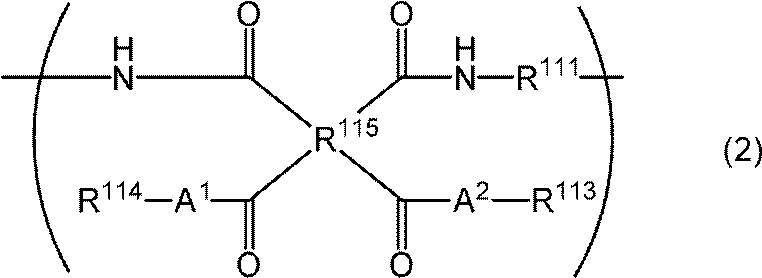
式(2)中、A1及びA2は、それぞれ独立に、酸素原子又は-NRz-を表し、R111は、2価の有機基を表し、R115は、4価の有機基を表し、R113及びR114は、それぞれ独立に、水素原子又は1価の有機基を表し、Rzは水素原子又は1価の有機基を表す。
<17> 半導体デバイスに用いられる、<1>~<16>のいずれか1つに記載の樹脂組成物。
<18> <1>~<17>のいずれか1つに記載の樹脂組成物を硬化してなる硬化物。
<19> <18>に記載の硬化物からなる層を2層以上含み、上記硬化物からなる層同士のいずれかの間に金属層を含む積層体。
<20> <1>~<17>のいずれか1つに記載の樹脂組成物を基材上に適用して膜を形成する膜形成工程、及び、
上記膜を50~450℃で加熱する加熱工程を含む、
硬化物の製造方法。
<21> <20>に記載の硬化物の製造方法を含む、積層体の製造方法。
<22> <20>に記載の硬化物の製造方法を含む、半導体デバイスの製造方法。
<23> <18>に記載の硬化物を含む、半導体デバイス。
<1> ポリイミド前駆体、及び、
フィラーを含み、
上記フィラーが、下記条件1及び条件2の少なくとも一方を満たすフィラーであるフィラーA1、並びに、フィラーA1とは異なるフィラーであるフィラーBを含む
樹脂組成物。
条件1:Naイオン換算でカチオン交換容量が0.1meq/g以上である
条件2:Clイオン換算でアニオン交換容量が0.1meq/g以上である
<2> 上記フィラーA1が少なくとも条件1を満たす、<1>に記載の樹脂組成物。
<3> 上記フィラーA1及び上記フィラーBの一次粒子径が、いずれも2μm以下である、<1>又は<2>に記載の樹脂組成物。
<4> 上記フィラーBのアスペクト比が3以上であり、上記フィラーA1のアスペクト比が3以下である、<1>~<3>のいずれか1つに記載の樹脂組成物。
<5> 上記フィラーA1の含有量が、樹脂組成物の全固形分に対して5質量%以下である、<1>~<4>のいずれか1つに記載の樹脂組成物。
<6> 上記フィラーA1が、Zr系化合物からなる粒子、Sb系化合物からなる粒子、Bi系化合物からなる粒子、Sb系化合物とBi系化合物の2元系からなる粒子、Mg系化合物とAl系化合物の2元系からなる粒子、Zr系化合物とBi系化合物の2元系からなる粒子、及び、Zr系化合物とMg系化合物とAl系化合物の3元系からなる粒子からなる群より選ばれた少なくとも1種の粒子である、<1>~<5>のいずれか1つに記載の樹脂組成物。
<7> ポリイミド前駆体、及び、
フィラーを含み、
上記フィラーが、Zr系化合物からなる粒子、Sb系化合物からなる粒子、Bi系化合物からなる粒子、Sb系化合物とBi系化合物の2元系からなる粒子、Mg系化合物とAl系化合物の2元系からなる粒子、Zr系化合物とBi系化合物の2元系からなる粒子、及び、Zr系化合物とMg系化合物とAl系化合物の3元系からなる粒子からなる群より選ばれた少なくとも1種の粒子であるフィラーA2、並びに、フィラーA2とは異なるフィラーであるフィラーBを含む
樹脂組成物。
<8> 上記フィラーA2のNaイオン換算でのカチオン交換容量が0.1meq/g以上である、<7>に記載の樹脂組成物。
<9> 上記フィラーA2及び上記フィラーBの一次粒子径が、いずれも2μm以下である、<7>又は<8>に記載の樹脂組成物。
<10> 上記フィラーBのアスペクト比が3以上であり、上記フィラーA2のアスペクト比が3以下である、<7>~<9>のいずれか1つに記載の樹脂組成物。
<11> 上記フィラーA2の含有量が、樹脂組成物の全固形分に対して5質量%以下である、<7>~<10>のいずれか1つに記載の樹脂組成物。
<12> 上記フィラーの少なくとも1種の含有量が、樹脂組成物の全固形分に対して10~70質量%である、<1>~<11>のいずれか1つに記載の樹脂組成物。
<13> 上記フィラーの合計含有量が、ポリイミド前駆体100質量部に対して30質量部以上である、<1>~<12>のいずれか1つに記載の樹脂組成物。
<14> 上記フィラーBの熱拡散率が1.0×10⁻⁶m2s-1以上であり、上記フィラーBの体積抵抗率が1.0×10¹¹Ω・cm以上である、<1>~<13>のいずれか1つに記載の樹脂組成物。
<15> 上記フィラーBが、窒化ホウ素、窒化アルミニウム、窒化ケイ素、酸化ケイ素、酸化アルミニウム、酸化マグネシウム、酸化亜鉛及び酸化ベリリウムからなる群より選ばれた少なくとも1種を含む、<1>~<14>のいずれか1つに記載の樹脂組成物。
<16> 上記ポリイミド前駆体が、下記式(2)で表される繰返し単位を含む、<1>~<15>のいずれか1つに記載の樹脂組成物。
式(2)中、A1及びA2は、それぞれ独立に、酸素原子又は-NRz-を表し、R111は、2価の有機基を表し、R115は、4価の有機基を表し、R113及びR114は、それぞれ独立に、水素原子又は1価の有機基を表し、Rzは水素原子又は1価の有機基を表す。
<17> 半導体デバイスに用いられる、<1>~<16>のいずれか1つに記載の樹脂組成物。
<18> <1>~<17>のいずれか1つに記載の樹脂組成物を硬化してなる硬化物。
<19> <18>に記載の硬化物からなる層を2層以上含み、上記硬化物からなる層同士のいずれかの間に金属層を含む積層体。
<20> <1>~<17>のいずれか1つに記載の樹脂組成物を基材上に適用して膜を形成する膜形成工程、及び、
上記膜を50~450℃で加熱する加熱工程を含む、
硬化物の製造方法。
<21> <20>に記載の硬化物の製造方法を含む、積層体の製造方法。
<22> <20>に記載の硬化物の製造方法を含む、半導体デバイスの製造方法。
<23> <18>に記載の硬化物を含む、半導体デバイス。
本発明によれば、信頼性に優れた硬化物が得られる樹脂組成物、上記樹脂組成物を硬化してなる硬化物、上記硬化物を含む積層体、上記硬化物の製造方法、上記積層体の製造方法、上記硬化物の製造方法を含む半導体デバイスの製造方法、並びに、上記硬化物を含む半導体デバイスが提供される。
以下、本発明の主要な実施形態について説明する。しかしながら、本発明は、明示した実施形態に限られるものではない。
本明細書において「~」という記号を用いて表される数値範囲は、「~」の前後に記載される数値をそれぞれ下限値及び上限値として含む範囲を意味する。
本明細書において「工程」との語は、独立した工程だけではなく、その工程の所期の作用が達成できる限りにおいて、他の工程と明確に区別できない工程も含む意味である。
本明細書における基(原子団)の表記において、置換及び無置換を記していない表記は、置換基を有しない基(原子団)と共に置換基を有する基(原子団)をも包含する。例えば、「アルキル基」とは、置換基を有しないアルキル基(無置換アルキル基)のみならず、置換基を有するアルキル基(置換アルキル基)をも包含する。
本明細書において「露光」とは、特に断らない限り、光を用いた露光のみならず、電子線、イオンビーム等の粒子線を用いた露光も含む。また、露光に用いられる光としては、水銀灯の輝線スペクトル、エキシマレーザーに代表される遠紫外線、極紫外線(EUV光)、X線、電子線等の活性光線又は放射線が挙げられる。
本明細書において、「(メタ)アクリレート」は、「アクリレート」及び「メタクリレート」の両方、又は、いずれかを意味し、「(メタ)アクリル」は、「アクリル」及び「メタクリル」の両方、又は、いずれかを意味し、「(メタ)アクリロイル」は、「アクリロイル」及び「メタクリロイル」の両方、又は、いずれかを意味する。
本明細書において、構造式中のMeはメチル基を表し、Etはエチル基を表し、Buはブチル基を表し、Phはフェニル基を表す。
本明細書において、全固形分とは、組成物の全成分から溶剤を除いた成分の総質量をいう。また本明細書において、固形分濃度とは、組成物の総質量に対する、溶剤を除く他の成分の質量百分率である。
本明細書において、重量平均分子量(Mw)及び数平均分子量(Mn)は、特に述べない限り、ゲル浸透クロマトグラフィ(GPC)法を用いて測定した値であり、ポリスチレン換算値として定義される。本明細書において、重量平均分子量(Mw)及び数平均分子量(Mn)は、例えば、HLC-8220GPC(東ソー(株)製)を用い、カラムとしてガードカラムHZ-L、TSKgel Super HZM-M、TSKgel Super HZ4000、TSKgel Super HZ3000、及び、TSKgel Super HZ2000(以上、東ソー(株)製)を直列に連結して用いることによって求めることができる。それらの分子量は特に述べない限り、溶離液としてTHF(テトラヒドロフラン)を用いて測定したものとする。ただし、溶解性が低い場合など、溶離液としてTHFが適していない場合にはNMP(N-メチル-2-ピロリドン)を用いることもできる。また、GPC測定における検出は特に述べない限り、UV線(紫外線)の波長254nm検出器を使用したものとする。
本明細書において、積層体を構成する各層の位置関係について、「上」又は「下」と記載したときには、注目している複数の層のうち基準となる層の上側又は下側に他の層があればよい。すなわち、基準となる層と上記他の層の間に、更に第3の層や要素が介在していてもよく、基準となる層と上記他の層は接している必要はない。特に断らない限り、基材に対し層が積み重なっていく方向を「上」と称し、又は、樹脂組成物層がある場合には、基材から樹脂組成物層へ向かう方向を「上」と称し、その反対方向を「下」と称する。なお、このような上下方向の設定は、本明細書中における便宜のためであり、実際の態様においては、本明細書における「上」方向は、鉛直上向きと異なることもありうる。
本明細書において、特段の記載がない限り、組成物は、組成物に含まれる各成分として、その成分に該当する2種以上の化合物を含んでもよい。また、特段の記載がない限り、組成物における各成分の含有量とは、その成分に該当する全ての化合物の合計含有量を意味する。
本明細書において、特に述べない限り、温度は23℃、気圧は101,325Pa(1気圧)、相対湿度は50%RHである。
本明細書において、好ましい態様の組み合わせは、より好ましい態様である。
本明細書において「~」という記号を用いて表される数値範囲は、「~」の前後に記載される数値をそれぞれ下限値及び上限値として含む範囲を意味する。
本明細書において「工程」との語は、独立した工程だけではなく、その工程の所期の作用が達成できる限りにおいて、他の工程と明確に区別できない工程も含む意味である。
本明細書における基(原子団)の表記において、置換及び無置換を記していない表記は、置換基を有しない基(原子団)と共に置換基を有する基(原子団)をも包含する。例えば、「アルキル基」とは、置換基を有しないアルキル基(無置換アルキル基)のみならず、置換基を有するアルキル基(置換アルキル基)をも包含する。
本明細書において「露光」とは、特に断らない限り、光を用いた露光のみならず、電子線、イオンビーム等の粒子線を用いた露光も含む。また、露光に用いられる光としては、水銀灯の輝線スペクトル、エキシマレーザーに代表される遠紫外線、極紫外線(EUV光)、X線、電子線等の活性光線又は放射線が挙げられる。
本明細書において、「(メタ)アクリレート」は、「アクリレート」及び「メタクリレート」の両方、又は、いずれかを意味し、「(メタ)アクリル」は、「アクリル」及び「メタクリル」の両方、又は、いずれかを意味し、「(メタ)アクリロイル」は、「アクリロイル」及び「メタクリロイル」の両方、又は、いずれかを意味する。
本明細書において、構造式中のMeはメチル基を表し、Etはエチル基を表し、Buはブチル基を表し、Phはフェニル基を表す。
本明細書において、全固形分とは、組成物の全成分から溶剤を除いた成分の総質量をいう。また本明細書において、固形分濃度とは、組成物の総質量に対する、溶剤を除く他の成分の質量百分率である。
本明細書において、重量平均分子量(Mw)及び数平均分子量(Mn)は、特に述べない限り、ゲル浸透クロマトグラフィ(GPC)法を用いて測定した値であり、ポリスチレン換算値として定義される。本明細書において、重量平均分子量(Mw)及び数平均分子量(Mn)は、例えば、HLC-8220GPC(東ソー(株)製)を用い、カラムとしてガードカラムHZ-L、TSKgel Super HZM-M、TSKgel Super HZ4000、TSKgel Super HZ3000、及び、TSKgel Super HZ2000(以上、東ソー(株)製)を直列に連結して用いることによって求めることができる。それらの分子量は特に述べない限り、溶離液としてTHF(テトラヒドロフラン)を用いて測定したものとする。ただし、溶解性が低い場合など、溶離液としてTHFが適していない場合にはNMP(N-メチル-2-ピロリドン)を用いることもできる。また、GPC測定における検出は特に述べない限り、UV線(紫外線)の波長254nm検出器を使用したものとする。
本明細書において、積層体を構成する各層の位置関係について、「上」又は「下」と記載したときには、注目している複数の層のうち基準となる層の上側又は下側に他の層があればよい。すなわち、基準となる層と上記他の層の間に、更に第3の層や要素が介在していてもよく、基準となる層と上記他の層は接している必要はない。特に断らない限り、基材に対し層が積み重なっていく方向を「上」と称し、又は、樹脂組成物層がある場合には、基材から樹脂組成物層へ向かう方向を「上」と称し、その反対方向を「下」と称する。なお、このような上下方向の設定は、本明細書中における便宜のためであり、実際の態様においては、本明細書における「上」方向は、鉛直上向きと異なることもありうる。
本明細書において、特段の記載がない限り、組成物は、組成物に含まれる各成分として、その成分に該当する2種以上の化合物を含んでもよい。また、特段の記載がない限り、組成物における各成分の含有量とは、その成分に該当する全ての化合物の合計含有量を意味する。
本明細書において、特に述べない限り、温度は23℃、気圧は101,325Pa(1気圧)、相対湿度は50%RHである。
本明細書において、好ましい態様の組み合わせは、より好ましい態様である。
(樹脂組成物)
本発明の第一の態様に係る樹脂組成物(以下、単に「第一の樹脂組成物」ともいう。)は、ポリイミド前駆体、及び、フィラーを含み、上記フィラーが、下記条件1及び条件2の少なくとも一方を満たすフィラーであるフィラーA1、並びに、フィラーA1とは異なるフィラーであるフィラーBを含む。
条件1:Naイオン換算でカチオン交換容量が0.1meq/g以上である
条件2:Clイオン換算でアニオン交換容量が0.1meq/g以上である
本発明の第二の態様に係る樹脂組成物(以下、単に「第二の樹脂組成物」ともいう。)は、ポリイミド前駆体、及び、フィラーを含み、上記フィラーが、Zr系化合物からなる粒子、Sb系化合物からなる粒子、Bi系化合物からなる粒子、Sb系化合物とBi系化合物の2元系からなる粒子、Mg系化合物とAl系化合物の2元系からなる粒子、Zr系化合物とBi系化合物の2元系からなる粒子、及び、Zr系化合物とMg系化合物とAl系化合物の3元系からなる粒子からなる群より選ばれた少なくとも1種の粒子であるフィラーA2、並びに、フィラーA2とは異なるフィラーであるフィラーBを含む。
以下、第一の樹脂組成物と第二の樹脂組成物とを合わせて単に「樹脂組成物」ともいう。
本発明の第一の態様に係る樹脂組成物(以下、単に「第一の樹脂組成物」ともいう。)は、ポリイミド前駆体、及び、フィラーを含み、上記フィラーが、下記条件1及び条件2の少なくとも一方を満たすフィラーであるフィラーA1、並びに、フィラーA1とは異なるフィラーであるフィラーBを含む。
条件1:Naイオン換算でカチオン交換容量が0.1meq/g以上である
条件2:Clイオン換算でアニオン交換容量が0.1meq/g以上である
本発明の第二の態様に係る樹脂組成物(以下、単に「第二の樹脂組成物」ともいう。)は、ポリイミド前駆体、及び、フィラーを含み、上記フィラーが、Zr系化合物からなる粒子、Sb系化合物からなる粒子、Bi系化合物からなる粒子、Sb系化合物とBi系化合物の2元系からなる粒子、Mg系化合物とAl系化合物の2元系からなる粒子、Zr系化合物とBi系化合物の2元系からなる粒子、及び、Zr系化合物とMg系化合物とAl系化合物の3元系からなる粒子からなる群より選ばれた少なくとも1種の粒子であるフィラーA2、並びに、フィラーA2とは異なるフィラーであるフィラーBを含む。
以下、第一の樹脂組成物と第二の樹脂組成物とを合わせて単に「樹脂組成物」ともいう。
本発明の樹脂組成物は、例えば、半導体デバイスの絶縁膜、再配線層用層間絶縁膜、ストレスバッファ膜等の形成に用いることができ、再配線層用層間絶縁膜の形成に用いられることが好ましい。
特に、本発明の樹脂組成物が、半導体デバイスに用いられることも、本発明の好ましい態様の1つである。
特に、本発明の樹脂組成物が、半導体デバイスに用いられることも、本発明の好ましい態様の1つである。
本発明の樹脂組成物によれば、信頼性に優れた硬化物が得られる。
上記効果が得られるメカニズムは不明であるが、下記のように推測される。
上記効果が得られるメカニズムは不明であるが、下記のように推測される。
本発明の第一の態様に係る組成物は、ポリイミド前駆体、及び、フィラーを含み、上記フィラーがフィラーA1及びフィラーBを含む。
本発明の第二の態様に係る組成物は、ポリイミド前駆体、及び、フィラーを含み、上記フィラーが、フィラーA2及びフィラーBを含む。
従来から、樹脂組成物に熱伝導性を有するフィラーを含有させることにより、組成物から形成される硬化物に熱伝導性を付与するなど、フィラーを用いた硬化物の改質が行われてきた。
本発明者らは、このようなフィラーを含有させた組成物に、フィラーA1又はフィラーA2を更に含有させることにより、硬化物と隣接する金属基材からの金属イオンのマイグレーションが抑制されるため、信頼性が向上することを見出した。
ここで、本発明の樹脂組成物は、フィラーA1又はフィラーA2、及び、フィラーBとを含む、すなわち、少なくとも2種のフィラーを含む。
本発明者らは、このような少なくとも2種のフィラーを含む組成物において、フィラー同士が凝集してしまうことを見出した。
そこで本発明者らは、組成物における樹脂を閉環したポリイミドではなく、ポリイミド前駆体とすることにより、フィラーの分散性が向上し、このようなフィラー同士の凝集が抑制されて、信頼性が更に向上することを見出した。これは、ポリイミド前駆体がフィラーの分散剤のように働くためであると推定している。
さらに、上記フィラーの形状に異方性がある場合、上記ポリイミド前駆体を用いることにより、フィラーの配向がランダムに近い状態となり、熱拡散率、熱膨張係数などの異方性が解消することを見出した。
本発明の第二の態様に係る組成物は、ポリイミド前駆体、及び、フィラーを含み、上記フィラーが、フィラーA2及びフィラーBを含む。
従来から、樹脂組成物に熱伝導性を有するフィラーを含有させることにより、組成物から形成される硬化物に熱伝導性を付与するなど、フィラーを用いた硬化物の改質が行われてきた。
本発明者らは、このようなフィラーを含有させた組成物に、フィラーA1又はフィラーA2を更に含有させることにより、硬化物と隣接する金属基材からの金属イオンのマイグレーションが抑制されるため、信頼性が向上することを見出した。
ここで、本発明の樹脂組成物は、フィラーA1又はフィラーA2、及び、フィラーBとを含む、すなわち、少なくとも2種のフィラーを含む。
本発明者らは、このような少なくとも2種のフィラーを含む組成物において、フィラー同士が凝集してしまうことを見出した。
そこで本発明者らは、組成物における樹脂を閉環したポリイミドではなく、ポリイミド前駆体とすることにより、フィラーの分散性が向上し、このようなフィラー同士の凝集が抑制されて、信頼性が更に向上することを見出した。これは、ポリイミド前駆体がフィラーの分散剤のように働くためであると推定している。
さらに、上記フィラーの形状に異方性がある場合、上記ポリイミド前駆体を用いることにより、フィラーの配向がランダムに近い状態となり、熱拡散率、熱膨張係数などの異方性が解消することを見出した。
ここで、特許文献1及び2には、ポリイミド前駆体と、フィラーA1又はフィラーA2と、フィラーBとを含有する樹脂組成物については記載されていない。
以下、本発明の樹脂組成物に含まれる成分について詳細に説明する。
<ポリイミド前駆体>
本発明の樹脂組成物は、ポリイミド前駆体(以下、「特定樹脂」ともいう。)を含む。
特定樹脂は重合性基を有することが好ましく、ラジカル重合性基を含むことがより好ましい。
特定樹脂がラジカル重合性基を有する場合、本発明の樹脂組成物は、ラジカル重合開始剤を含むことが好ましく、ラジカル重合開始剤を含み、かつ、ラジカル架橋剤を含むことがより好ましい。さらに必要に応じて、増感剤を含むことができる。
本発明の樹脂組成物は、ポリイミド前駆体(以下、「特定樹脂」ともいう。)を含む。
特定樹脂は重合性基を有することが好ましく、ラジカル重合性基を含むことがより好ましい。
特定樹脂がラジカル重合性基を有する場合、本発明の樹脂組成物は、ラジカル重合開始剤を含むことが好ましく、ラジカル重合開始剤を含み、かつ、ラジカル架橋剤を含むことがより好ましい。さらに必要に応じて、増感剤を含むことができる。
本発明で用いるポリイミド前駆体は、その種類等は特に限定されないが、下記式(2)で表される繰返し単位を含むことが好ましい。
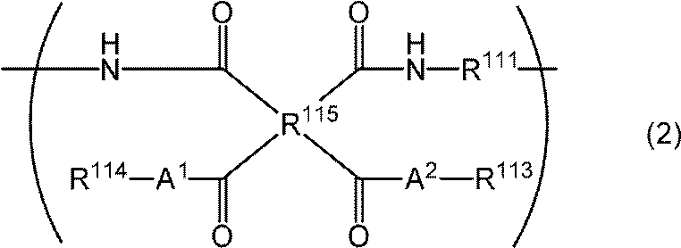
式(2)中、A1及びA2は、それぞれ独立に、酸素原子又は-NRz-を表し、R111は、2価の有機基を表し、R115は、4価の有機基を表し、R113及びR114は、それぞれ独立に、水素原子又は1価の有機基を表し、Rzは水素原子又は1価の有機基を表す。
式(2)中、A1及びA2は、それぞれ独立に、酸素原子又は-NRz-を表し、R111は、2価の有機基を表し、R115は、4価の有機基を表し、R113及びR114は、それぞれ独立に、水素原子又は1価の有機基を表し、Rzは水素原子又は1価の有機基を表す。
式(2)におけるA1及びA2は、それぞれ独立に、酸素原子又は-NRz-を表し、酸素原子が好ましい。
Rzは水素原子又は1価の有機基を表し、水素原子が好ましい。
式(2)におけるR111は、2価の有機基を表す。2価の有機基としては、直鎖又は分岐の脂肪族基、環状の脂肪族基及び芳香族基を含む基が例示され、炭素数2~20の直鎖又は分岐の脂肪族基、炭素数3~20の環状の脂肪族基、炭素数3~20の芳香族基、又は、これらの組み合わせからなる基が好ましく、炭素数6~20の芳香族基を含む基がより好ましい。上記直鎖又は分岐の脂肪族基は鎖中の炭化水素基がヘテロ原子を含む基で置換されていてもよく、上記環状の脂肪族基および芳香族基は環員の炭化水素基がヘテロ原子を含む基で置換されていてもよい。式(2)におけるR111の例としては、-Ar-および-Ar-L-Ar-で表される基が挙げられ、-Ar-L-Ar-で表される基が好ましい。但し、Arは、それぞれ独立に、芳香族基であり、Lは、単結合、又は、フッ素原子で置換されていてもよい炭素数1~10の脂肪族炭化水素基、-O-、-CO-、-S-、-SO2-若しくは-NHCO-、あるいは、上記の2つ以上の組み合わせからなる基である。これらの好ましい範囲は、上述のとおりである。
Rzは水素原子又は1価の有機基を表し、水素原子が好ましい。
式(2)におけるR111は、2価の有機基を表す。2価の有機基としては、直鎖又は分岐の脂肪族基、環状の脂肪族基及び芳香族基を含む基が例示され、炭素数2~20の直鎖又は分岐の脂肪族基、炭素数3~20の環状の脂肪族基、炭素数3~20の芳香族基、又は、これらの組み合わせからなる基が好ましく、炭素数6~20の芳香族基を含む基がより好ましい。上記直鎖又は分岐の脂肪族基は鎖中の炭化水素基がヘテロ原子を含む基で置換されていてもよく、上記環状の脂肪族基および芳香族基は環員の炭化水素基がヘテロ原子を含む基で置換されていてもよい。式(2)におけるR111の例としては、-Ar-および-Ar-L-Ar-で表される基が挙げられ、-Ar-L-Ar-で表される基が好ましい。但し、Arは、それぞれ独立に、芳香族基であり、Lは、単結合、又は、フッ素原子で置換されていてもよい炭素数1~10の脂肪族炭化水素基、-O-、-CO-、-S-、-SO2-若しくは-NHCO-、あるいは、上記の2つ以上の組み合わせからなる基である。これらの好ましい範囲は、上述のとおりである。
R111は、ジアミンから誘導されることが好ましい。ポリイミド前駆体の製造に用いられるジアミンとしては、直鎖又は分岐の脂肪族、環状の脂肪族又は芳香族ジアミンなどが挙げられる。ジアミンは、1種のみ用いてもよいし、2種以上用いてもよい。
具体的には、R111は、炭素数2~20の直鎖又は分岐の脂肪族基、炭素数3~20の環状の脂肪族基、炭素数3~20の芳香族基、又は、これらの組み合わせからなる基を含むジアミンであることが好ましく、炭素数6~20の芳香族基を含むジアミンであることがより好ましい。上記直鎖又は分岐の脂肪族基は鎖中の炭化水素基がヘテロ原子を含む基で置換されていてもよく上記環状の脂肪族基および芳香族基は環員の炭化水素基がヘテロ原子を含む基で置換されていてもよい。芳香族基を含む基の例としては、下記が挙げられる。
具体的には、R111は、炭素数2~20の直鎖又は分岐の脂肪族基、炭素数3~20の環状の脂肪族基、炭素数3~20の芳香族基、又は、これらの組み合わせからなる基を含むジアミンであることが好ましく、炭素数6~20の芳香族基を含むジアミンであることがより好ましい。上記直鎖又は分岐の脂肪族基は鎖中の炭化水素基がヘテロ原子を含む基で置換されていてもよく上記環状の脂肪族基および芳香族基は環員の炭化水素基がヘテロ原子を含む基で置換されていてもよい。芳香族基を含む基の例としては、下記が挙げられる。
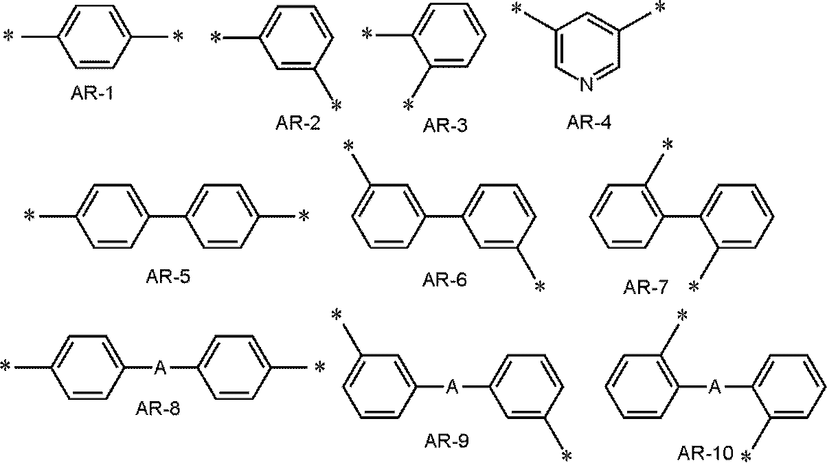
式中、Aは単結合又は2価の連結基を表し、単結合、又は、フッ素原子で置換されていてもよい炭素数1~10の脂肪族炭化水素基、-O-、-C(=O)-、-S-、-SO2-、-NHCO-、又は、これらの組み合わせから選択される基であることが好ましく、単結合、又は、フッ素原子で置換されていてもよい炭素数1~3のアルキレン基、-O-、-C(=O)-、-S-、若しくは、-SO2-から選択される基であることがより好ましく、-CH2-、-O-、-S-、-SO2-、-C(CF3)2-、又は、-C(CH3)2-であることが更に好ましい。
式中、*は他の構造との結合部位を表す。
ジアミンとしては、具体的には、1,2-ジアミノエタン、1,2-ジアミノプロパン、1,3-ジアミノプロパン、1,4-ジアミノブタン又は1,6-ジアミノヘキサン;
1,2-又は1,3-ジアミノシクロペンタン、1,2-、1,3-又は1,4-ジアミノシクロヘキサン、1,2-、1,3-又は1,4-ビス(アミノメチル)シクロヘキサン、ビス-(4-アミノシクロヘキシル)メタン、ビス-(3-アミノシクロヘキシル)メタン、4,4’-ジアミノ-3,3’-ジメチルシクロヘキシルメタン及びイソホロンジアミン;
m-又はp-フェニレンジアミン、ジアミノトルエン、4,4’-又は3,3’-ジアミノビフェニル、4,4’-ジアミノジフェニルエーテル、3,3-ジアミノジフェニルエーテル、4,4’-又は3,3’-ジアミノジフェニルメタン、4,4’-又は3,3’-ジアミノジフェニルスルホン、4,4’-又は3,3’-ジアミノジフェニルスルフィド、4,4’-又は3,3’-ジアミノベンゾフェノン、3,3’-ジメチル-4,4’-ジアミノビフェニル、2,2’-ジメチル-4,4’-ジアミノビフェニル、3,3’-ジメトキシ-4,4’-ジアミノビフェニル、2,2-ビス(4-アミノフェニル)プロパン、2,2-ビス(4-アミノフェニル)ヘキサフルオロプロパン、2,2-ビス(3-ヒドロキシ-4-アミノフェニル)プロパン、2,2-ビス(3-ヒドロキシ-4-アミノフェニル)ヘキサフルオロプロパン、2,2-ビス(3-アミノ-4-ヒドロキシフェニル)プロパン、2,2-ビス(3-アミノ-4-ヒドロキシフェニル)ヘキサフルオロプロパン、ビス(3-アミノ-4-ヒドロキシフェニル)スルホン、ビス(4-アミノ-3-ヒドロキシフェニル)スルホン、4,4’-ジアミノパラテルフェニル、4,4’-ビス(4-アミノフェノキシ)ビフェニル、ビス[4-(4-アミノフェノキシ)フェニル]スルホン、ビス[4-(3-アミノフェノキシ)フェニル]スルホン、ビス[4-(2-アミノフェノキシ)フェニル]スルホン、1,4-ビス(4-アミノフェノキシ)ベンゼン、9,10-ビス(4-アミノフェニル)アントラセン、3,3’-ジメチル-4,4’-ジアミノジフェニルスルホン、1,3-ビス(4-アミノフェノキシ)ベンゼン、1,3-ビス(3-アミノフェノキシ)ベンゼン、1,3-ビス(4-アミノフェニル)ベンゼン、3,3’-ジエチル-4,4’-ジアミノジフェニルメタン、3,3’-ジメチル-4,4’-ジアミノジフェニルメタン、4,4’-ジアミノオクタフルオロビフェニル、2,2-ビス[4-(4-アミノフェノキシ)フェニル]プロパン、2,2-ビス[4-(4-アミノフェノキシ)フェニル]ヘキサフルオロプロパン、9,9-ビス(4-アミノフェニル)-10-ヒドロアントラセン、3,3’,4,4’-テトラアミノビフェニル、3,3’,4,4’-テトラアミノジフェニルエーテル、1,4-ジアミノアントラキノン、1,5-ジアミノアントラキノン、3,3-ジヒドロキシ-4,4’-ジアミノビフェニル、9,9’-ビス(4-アミノフェニル)フルオレン、4,4’-ジメチル-3,3’-ジアミノジフェニルスルホン、3,3’,5,5’-テトラメチル-4,4’-ジアミノジフェニルメタン、2,4-及び2,5-ジアミノクメン、2,5-ジメチル-p-フェニレンジアミン、アセトグアナミン、2,3,5,6-テトラメチル-p-フェニレンジアミン、2,4,6-トリメチル-m-フェニレンジアミン、ビス(3-アミノプロピル)テトラメチルジシロキサン、ビス(p-アミノフェニル)オクタメチルペンタシロキサン、2,7-ジアミノフルオレン、2,5-ジアミノピリジン、1,2-ビス(4-アミノフェニル)エタン、ジアミノベンズアニリド、ジアミノ安息香酸のエステル、1,5-ジアミノナフタレン、ジアミノベンゾトリフルオライド、1,3-ビス(4-アミノフェニル)ヘキサフルオロプロパン、1,4-ビス(4-アミノフェニル)オクタフルオロブタン、1,5-ビス(4-アミノフェニル)デカフルオロペンタン、1,7-ビス(4-アミノフェニル)テトラデカフルオロヘプタン、2,2-ビス[4-(3-アミノフェノキシ)フェニル]ヘキサフルオロプロパン、2,2-ビス[4-(2-アミノフェノキシ)フェニル]ヘキサフルオロプロパン、2,2-ビス[4-(4-アミノフェノキシ)-3,5-ジメチルフェニル]ヘキサフルオロプロパン、2,2-ビス[4-(4-アミノフェノキシ)-3,5-ビス(トリフルオロメチル)フェニル]ヘキサフルオロプロパン、p-ビス(4-アミノ-2-トリフルオロメチルフェノキシ)ベンゼン、4,4’-ビス(4-アミノ-2-トリフルオロメチルフェノキシ)ビフェニル、4,4’-ビス(4-アミノ-3-トリフルオロメチルフェノキシ)ビフェニル、4,4’-ビス(4-アミノ-2-トリフルオロメチルフェノキシ)ジフェニルスルホン、4,4’-ビス(3-アミノ-5-トリフルオロメチルフェノキシ)ジフェニルスルホン、2,2-ビス[4-(4-アミノ-3-トリフルオロメチルフェノキシ)フェニル]ヘキサフルオロプロパン、3,3’,5,5’-テトラメチル-4,4’-ジアミノビフェニル、4,4’-ジアミノ-2,2’-ビス(トリフルオロメチル)ビフェニル、2,2’,5,5’,6,6’-ヘキサフルオロトリジン及び4,4’-ジアミノクアテルフェニルから選ばれる少なくとも1種のジアミンが挙げられる。
1,2-又は1,3-ジアミノシクロペンタン、1,2-、1,3-又は1,4-ジアミノシクロヘキサン、1,2-、1,3-又は1,4-ビス(アミノメチル)シクロヘキサン、ビス-(4-アミノシクロヘキシル)メタン、ビス-(3-アミノシクロヘキシル)メタン、4,4’-ジアミノ-3,3’-ジメチルシクロヘキシルメタン及びイソホロンジアミン;
m-又はp-フェニレンジアミン、ジアミノトルエン、4,4’-又は3,3’-ジアミノビフェニル、4,4’-ジアミノジフェニルエーテル、3,3-ジアミノジフェニルエーテル、4,4’-又は3,3’-ジアミノジフェニルメタン、4,4’-又は3,3’-ジアミノジフェニルスルホン、4,4’-又は3,3’-ジアミノジフェニルスルフィド、4,4’-又は3,3’-ジアミノベンゾフェノン、3,3’-ジメチル-4,4’-ジアミノビフェニル、2,2’-ジメチル-4,4’-ジアミノビフェニル、3,3’-ジメトキシ-4,4’-ジアミノビフェニル、2,2-ビス(4-アミノフェニル)プロパン、2,2-ビス(4-アミノフェニル)ヘキサフルオロプロパン、2,2-ビス(3-ヒドロキシ-4-アミノフェニル)プロパン、2,2-ビス(3-ヒドロキシ-4-アミノフェニル)ヘキサフルオロプロパン、2,2-ビス(3-アミノ-4-ヒドロキシフェニル)プロパン、2,2-ビス(3-アミノ-4-ヒドロキシフェニル)ヘキサフルオロプロパン、ビス(3-アミノ-4-ヒドロキシフェニル)スルホン、ビス(4-アミノ-3-ヒドロキシフェニル)スルホン、4,4’-ジアミノパラテルフェニル、4,4’-ビス(4-アミノフェノキシ)ビフェニル、ビス[4-(4-アミノフェノキシ)フェニル]スルホン、ビス[4-(3-アミノフェノキシ)フェニル]スルホン、ビス[4-(2-アミノフェノキシ)フェニル]スルホン、1,4-ビス(4-アミノフェノキシ)ベンゼン、9,10-ビス(4-アミノフェニル)アントラセン、3,3’-ジメチル-4,4’-ジアミノジフェニルスルホン、1,3-ビス(4-アミノフェノキシ)ベンゼン、1,3-ビス(3-アミノフェノキシ)ベンゼン、1,3-ビス(4-アミノフェニル)ベンゼン、3,3’-ジエチル-4,4’-ジアミノジフェニルメタン、3,3’-ジメチル-4,4’-ジアミノジフェニルメタン、4,4’-ジアミノオクタフルオロビフェニル、2,2-ビス[4-(4-アミノフェノキシ)フェニル]プロパン、2,2-ビス[4-(4-アミノフェノキシ)フェニル]ヘキサフルオロプロパン、9,9-ビス(4-アミノフェニル)-10-ヒドロアントラセン、3,3’,4,4’-テトラアミノビフェニル、3,3’,4,4’-テトラアミノジフェニルエーテル、1,4-ジアミノアントラキノン、1,5-ジアミノアントラキノン、3,3-ジヒドロキシ-4,4’-ジアミノビフェニル、9,9’-ビス(4-アミノフェニル)フルオレン、4,4’-ジメチル-3,3’-ジアミノジフェニルスルホン、3,3’,5,5’-テトラメチル-4,4’-ジアミノジフェニルメタン、2,4-及び2,5-ジアミノクメン、2,5-ジメチル-p-フェニレンジアミン、アセトグアナミン、2,3,5,6-テトラメチル-p-フェニレンジアミン、2,4,6-トリメチル-m-フェニレンジアミン、ビス(3-アミノプロピル)テトラメチルジシロキサン、ビス(p-アミノフェニル)オクタメチルペンタシロキサン、2,7-ジアミノフルオレン、2,5-ジアミノピリジン、1,2-ビス(4-アミノフェニル)エタン、ジアミノベンズアニリド、ジアミノ安息香酸のエステル、1,5-ジアミノナフタレン、ジアミノベンゾトリフルオライド、1,3-ビス(4-アミノフェニル)ヘキサフルオロプロパン、1,4-ビス(4-アミノフェニル)オクタフルオロブタン、1,5-ビス(4-アミノフェニル)デカフルオロペンタン、1,7-ビス(4-アミノフェニル)テトラデカフルオロヘプタン、2,2-ビス[4-(3-アミノフェノキシ)フェニル]ヘキサフルオロプロパン、2,2-ビス[4-(2-アミノフェノキシ)フェニル]ヘキサフルオロプロパン、2,2-ビス[4-(4-アミノフェノキシ)-3,5-ジメチルフェニル]ヘキサフルオロプロパン、2,2-ビス[4-(4-アミノフェノキシ)-3,5-ビス(トリフルオロメチル)フェニル]ヘキサフルオロプロパン、p-ビス(4-アミノ-2-トリフルオロメチルフェノキシ)ベンゼン、4,4’-ビス(4-アミノ-2-トリフルオロメチルフェノキシ)ビフェニル、4,4’-ビス(4-アミノ-3-トリフルオロメチルフェノキシ)ビフェニル、4,4’-ビス(4-アミノ-2-トリフルオロメチルフェノキシ)ジフェニルスルホン、4,4’-ビス(3-アミノ-5-トリフルオロメチルフェノキシ)ジフェニルスルホン、2,2-ビス[4-(4-アミノ-3-トリフルオロメチルフェノキシ)フェニル]ヘキサフルオロプロパン、3,3’,5,5’-テトラメチル-4,4’-ジアミノビフェニル、4,4’-ジアミノ-2,2’-ビス(トリフルオロメチル)ビフェニル、2,2’,5,5’,6,6’-ヘキサフルオロトリジン及び4,4’-ジアミノクアテルフェニルから選ばれる少なくとも1種のジアミンが挙げられる。
また、国際公開第2017/038598号の段落0030~0031に記載のジアミン(DA-1)~(DA-18)も好ましい。
また、国際公開第2017/038598号の段落0032~0034に記載の2つ以上のアルキレングリコール単位を主鎖にもつジアミンも好ましく用いられる。
R111は、得られる有機膜の柔軟性の観点から、-Ar-L-Ar-で表されることが好ましい。但し、Arは、それぞれ独立に、芳香族基であり、Lは、フッ素原子で置換されていてもよい炭素数1~10の脂肪族炭化水素基、-O-、-CO-、-S-、-SO2-又は-NHCO-、あるいは、上記の2つ以上の組み合わせからなる基である。Arは、フェニレン基が好ましく、Lは、フッ素原子で置換されていてもよい炭素数1又は2の脂肪族炭化水素基、-O-、-CO-、-S-又は-SO2-が好ましい。ここでの脂肪族炭化水素基は、アルキレン基が好ましい。
また、R111は、i線透過率の観点から、下記式(51)又は式(61)で表される2価の有機基であることが好ましい。特に、i線透過率、入手のし易さの観点から、式(61)で表される2価の有機基であることがより好ましい。
式(51)
式(51)中、R50~R57は、それぞれ独立に、水素原子、フッ素原子又は1価の有機基であり、R50~R57の少なくとも1つは、フッ素原子、メチル基又はトリフルオロメチル基であり、*はそれぞれ独立に、式(2)中の窒素原子との結合部位を表す。
R50~R57の1価の有機基としては、炭素数1~10(好ましくは炭素数1~6)の無置換のアルキル基、炭素数1~10(好ましくは炭素数1~6)のフッ化アルキル基等が挙げられる。
式(61)中、R58及びR59は、それぞれ独立に、フッ素原子、メチル基、又はトリフルオロメチル基であり、*はそれぞれ独立に、式(2)中の窒素原子との結合部位を表す。
式(51)又は式(61)の構造を与えるジアミンとしては、2,2’-ジメチルベンジジン、2,2’-ビス(トリフルオロメチル)-4,4’-ジアミノビフェニル、2,2’-ビス(フルオロ)-4,4’-ジアミノビフェニル、4,4’-ジアミノオクタフルオロビフェニル等が挙げられる。これらは1種又は2種以上を組み合わせて用いてもよい。
式(51)
式(51)中、R50~R57は、それぞれ独立に、水素原子、フッ素原子又は1価の有機基であり、R50~R57の少なくとも1つは、フッ素原子、メチル基又はトリフルオロメチル基であり、*はそれぞれ独立に、式(2)中の窒素原子との結合部位を表す。
R50~R57の1価の有機基としては、炭素数1~10(好ましくは炭素数1~6)の無置換のアルキル基、炭素数1~10(好ましくは炭素数1~6)のフッ化アルキル基等が挙げられる。
式(61)中、R58及びR59は、それぞれ独立に、フッ素原子、メチル基、又はトリフルオロメチル基であり、*はそれぞれ独立に、式(2)中の窒素原子との結合部位を表す。
式(51)又は式(61)の構造を与えるジアミンとしては、2,2’-ジメチルベンジジン、2,2’-ビス(トリフルオロメチル)-4,4’-ジアミノビフェニル、2,2’-ビス(フルオロ)-4,4’-ジアミノビフェニル、4,4’-ジアミノオクタフルオロビフェニル等が挙げられる。これらは1種又は2種以上を組み合わせて用いてもよい。
式(2)におけるR115は、4価の有機基を表す。4価の有機基としては、芳香環を含む4価の有機基が好ましく、下記式(5)又は式(6)で表される基がより好ましい。
式(5)又は式(6)中、*はそれぞれ独立に、他の構造との結合部位を表す。
式(5)中、R112は単結合又は2価の連結基であり、単結合、又は、フッ素原子で置換されていてもよい炭素数1~10の脂肪族炭化水素基、-O-、-CO-、-S-、-SO2-、及び-NHCO-、ならびに、これらの組み合わせから選択される基であることが好ましく、単結合、または、フッ素原子で置換されていてもよい炭素数1~3のアルキレン基、-O-、-CO-、-S-及び-SO2-から選択される基であることがより好ましく、-CH2-、-C(CF3)2-、-C(CH3)2-、-O-、-CO-、-S-及び-SO2-からなる群より選択される2価の基であることが更に好ましい。
式(5)又は式(6)中、*はそれぞれ独立に、他の構造との結合部位を表す。
式(5)中、R112は単結合又は2価の連結基であり、単結合、又は、フッ素原子で置換されていてもよい炭素数1~10の脂肪族炭化水素基、-O-、-CO-、-S-、-SO2-、及び-NHCO-、ならびに、これらの組み合わせから選択される基であることが好ましく、単結合、または、フッ素原子で置換されていてもよい炭素数1~3のアルキレン基、-O-、-CO-、-S-及び-SO2-から選択される基であることがより好ましく、-CH2-、-C(CF3)2-、-C(CH3)2-、-O-、-CO-、-S-及び-SO2-からなる群より選択される2価の基であることが更に好ましい。
R115は、具体的には、テトラカルボン酸二無水物から無水物基の除去後に残存するテトラカルボン酸残基などが挙げられる。ポリイミド前駆体は、R115に該当する構造として、テトラカルボン酸二無水物残基を、1種のみ含んでもよいし、2種以上含んでもよい。
テトラカルボン酸二無水物は、下記式(O)で表されることが好ましい。
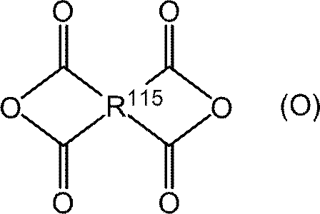
式(O)中、R115は、4価の有機基を表す。R115は式(2)におけるR115と同義であり、好ましい範囲も同様である。
テトラカルボン酸二無水物は、下記式(O)で表されることが好ましい。
式(O)中、R115は、4価の有機基を表す。R115は式(2)におけるR115と同義であり、好ましい範囲も同様である。
テトラカルボン酸二無水物の具体例としては、ピロメリット酸二無水物(PMDA)、3,3’,4,4’-ビフェニルテトラカルボン酸二無水物、3,3’,4,4’-ジフェニルスルフィドテトラカルボン酸二無水物、3,3’,4,4’-ジフェニルスルホンテトラカルボン酸二無水物、3,3’,4,4’-ベンゾフェノンテトラカルボン酸二無水物、3,3’,4,4’-ジフェニルメタンテトラカルボン酸二無水物、2,2’,3,3’-ジフェニルメタンテトラカルボン酸二無水物、2,3,3’,4’-ビフェニルテトラカルボン酸二無水物、2,3,3’,4’-ベンゾフェノンテトラカルボン酸二無水物、4,4’-オキシジフタル酸二無水物、2,3,6,7-ナフタレンテトラカルボン酸二無水物、1,4,5,7-ナフタレンテトラカルボン酸二無水物、2,2-ビス(3,4-ジカルボキシフェニル)プロパン二無水物、2,2-ビス(2,3-ジカルボキシフェニル)プロパン二無水物、2,2-ビス(3,4-ジカルボキシフェニル)ヘキサフルオロプロパン二無水物、1,3-ジフェニルヘキサフルオロプロパン-3,3,4,4-テトラカルボン酸二無水物、1,4,5,6-ナフタレンテトラカルボン酸二無水物、2,2’,3,3’-ジフェニルテトラカルボン酸二無水物、3,4,9,10-ペリレンテトラカルボン酸二無水物、1,2,4,5-ナフタレンテトラカルボン酸二無水物、1,4,5,8-ナフタレンテトラカルボン酸二無水物、1,8,9,10-フェナントレンテトラカルボン酸二無水物、1,1-ビス(2,3-ジカルボキシフェニル)エタン二無水物、1,1-ビス(3,4-ジカルボキシフェニル)エタン二無水物、1,2,3,4-ベンゼンテトラカルボン酸二無水物、ならびに、これらの炭素数1~6のアルキル及び炭素数1~6のアルコキシ誘導体が挙げられる。
また、国際公開第2017/038598号の段落0038に記載のテトラカルボン酸二無水物(DAA-1)~(DAA-5)も好ましい例として挙げられる。
式(2)において、R111とR115の少なくとも一方がOH基を有することも可能である。より具体的には、R111として、ビスアミノフェノール誘導体の残基が挙げられる。
式(2)におけるR113及びR114は、それぞれ独立に、水素原子又は1価の有機基を表す。1価の有機基としては、直鎖又は分岐のアルキル基、環状アルキル基、芳香族基、又はポリアルキレンオキシ基を含むことが好ましい。また、R113及びR114の少なくとも一方が重合性基を含むことが好ましく、両方が重合性基を含むことがより好ましい。R113及びR114の少なくとも一方が2以上の重合性基を含むことも好ましい。重合性基としては、熱、ラジカル等の作用により、架橋反応することが可能な基であって、ラジカル重合性基が好ましい。重合性基の具体例としては、エチレン性不飽和結合を有する基、アルコキシメチル基、ヒドロキシメチル基、アシルオキシメチル基、エポキシ基、オキセタニル基、ベンゾオキサゾリル基、ブロックイソシアネート基、アミノ基が挙げられる。ポリイミド前駆体が有するラジカル重合性基としては、エチレン性不飽和結合を有する基が好ましい。
エチレン性不飽和結合を有する基としては、ビニル基、アリル基、イソアリル基、2-メチルアリル基、ビニル基と直接結合した芳香環を有する基(例えば、ビニルフェニル基など)、(メタ)アクリルアミド基、(メタ)アクリロイルオキシ基、下記式(III)で表される基などが挙げられ、下記式(III)で表される基が好ましい。
エチレン性不飽和結合を有する基としては、ビニル基、アリル基、イソアリル基、2-メチルアリル基、ビニル基と直接結合した芳香環を有する基(例えば、ビニルフェニル基など)、(メタ)アクリルアミド基、(メタ)アクリロイルオキシ基、下記式(III)で表される基などが挙げられ、下記式(III)で表される基が好ましい。
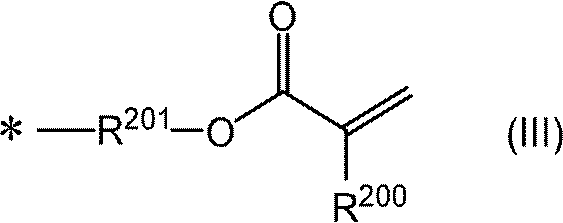
式(III)において、R200は、水素原子、メチル基、エチル基又はメチロール基を表し、水素原子又はメチル基が好ましい。
式(III)において、*は他の構造との結合部位を表す。
式(III)において、R201は、炭素数2~12のアルキレン基、-CH2CH(OH)CH2-、シクロアルキレン基又はポリアルキレンオキシ基を表す。
好適なR201の例は、エチレン基、プロピレン基、トリメチレン基、テトラメチレン基、ペンタメチレン基、ヘキサメチレン基、オクタメチレン基、ドデカメチレン基等のアルキレン基、1,2-ブタンジイル基、1,3-ブタンジイル基、-CH2CH(OH)CH2-、ポリアルキレンオキシ基が挙げられ、エチレン基、プロピレン基等のアルキレン基、-CH2CH(OH)CH2-、シクロヘキシル基、ポリアルキレンオキシ基がより好ましく、エチレン基、プロピレン基等のアルキレン基、又はポリアルキレンオキシ基が更に好ましい。
本発明において、ポリアルキレンオキシ基とは、アルキレンオキシ基が2以上直接結合した基をいう。ポリアルキレンオキシ基に含まれる複数のアルキレンオキシ基におけるアルキレン基は、それぞれ同一であっても異なっていてもよい。
ポリアルキレンオキシ基が、アルキレン基が異なる複数種のアルキレンオキシ基を含む場合、ポリアルキレンオキシ基におけるアルキレンオキシ基の配列は、ランダムな配列であってもよいし、ブロックを有する配列であってもよいし、交互等のパターンを有する配列であってもよい。
上記アルキレン基の炭素数(アルキレン基が置換基を有する場合、置換基の炭素数を含む)は、2以上であることが好ましく、2~10であることがより好ましく、2~6であることがより好ましく、2~5であることが更に好ましく、2~4であることが一層好ましく、2又は3であることがより更に好ましく、2であることが特に好ましい。
また、上記アルキレン基は、置換基を有していてもよい。好ましい置換基としては、アルキル基、アリール基、ハロゲン原子等が挙げられる。
また、ポリアルキレンオキシ基に含まれるアルキレンオキシ基の数(ポリアルキレンオキシ基の繰返し数)は、2~20が好ましく、2~10がより好ましく、2~6が更に好ましい。
ポリアルキレンオキシ基としては、溶剤溶解性及び耐溶剤性の観点からは、ポリエチレンオキシ基、ポリプロピレンオキシ基、ポリトリメチレンオキシ基、ポリテトラメチレンオキシ基、又は、複数のエチレンオキシ基と複数のプロピレンオキシ基とが結合した基が好ましく、ポリエチレンオキシ基又はポリプロピレンオキシ基がより好ましく、ポリエチレンオキシ基が更に好ましい。上記複数のエチレンオキシ基と複数のプロピレンオキシ基とが結合した基において、エチレンオキシ基とプロピレンオキシ基とはランダムに配列していてもよいし、ブロックを形成して配列していてもよいし、交互等のパターン状に配列していてもよい。これらの基におけるエチレンオキシ基等の繰返し数の好ましい態様は上述の通りである。
式(III)において、*は他の構造との結合部位を表す。
式(III)において、R201は、炭素数2~12のアルキレン基、-CH2CH(OH)CH2-、シクロアルキレン基又はポリアルキレンオキシ基を表す。
好適なR201の例は、エチレン基、プロピレン基、トリメチレン基、テトラメチレン基、ペンタメチレン基、ヘキサメチレン基、オクタメチレン基、ドデカメチレン基等のアルキレン基、1,2-ブタンジイル基、1,3-ブタンジイル基、-CH2CH(OH)CH2-、ポリアルキレンオキシ基が挙げられ、エチレン基、プロピレン基等のアルキレン基、-CH2CH(OH)CH2-、シクロヘキシル基、ポリアルキレンオキシ基がより好ましく、エチレン基、プロピレン基等のアルキレン基、又はポリアルキレンオキシ基が更に好ましい。
本発明において、ポリアルキレンオキシ基とは、アルキレンオキシ基が2以上直接結合した基をいう。ポリアルキレンオキシ基に含まれる複数のアルキレンオキシ基におけるアルキレン基は、それぞれ同一であっても異なっていてもよい。
ポリアルキレンオキシ基が、アルキレン基が異なる複数種のアルキレンオキシ基を含む場合、ポリアルキレンオキシ基におけるアルキレンオキシ基の配列は、ランダムな配列であってもよいし、ブロックを有する配列であってもよいし、交互等のパターンを有する配列であってもよい。
上記アルキレン基の炭素数(アルキレン基が置換基を有する場合、置換基の炭素数を含む)は、2以上であることが好ましく、2~10であることがより好ましく、2~6であることがより好ましく、2~5であることが更に好ましく、2~4であることが一層好ましく、2又は3であることがより更に好ましく、2であることが特に好ましい。
また、上記アルキレン基は、置換基を有していてもよい。好ましい置換基としては、アルキル基、アリール基、ハロゲン原子等が挙げられる。
また、ポリアルキレンオキシ基に含まれるアルキレンオキシ基の数(ポリアルキレンオキシ基の繰返し数)は、2~20が好ましく、2~10がより好ましく、2~6が更に好ましい。
ポリアルキレンオキシ基としては、溶剤溶解性及び耐溶剤性の観点からは、ポリエチレンオキシ基、ポリプロピレンオキシ基、ポリトリメチレンオキシ基、ポリテトラメチレンオキシ基、又は、複数のエチレンオキシ基と複数のプロピレンオキシ基とが結合した基が好ましく、ポリエチレンオキシ基又はポリプロピレンオキシ基がより好ましく、ポリエチレンオキシ基が更に好ましい。上記複数のエチレンオキシ基と複数のプロピレンオキシ基とが結合した基において、エチレンオキシ基とプロピレンオキシ基とはランダムに配列していてもよいし、ブロックを形成して配列していてもよいし、交互等のパターン状に配列していてもよい。これらの基におけるエチレンオキシ基等の繰返し数の好ましい態様は上述の通りである。
式(2)において、R113が水素原子である場合、又は、R114が水素原子である場合、ポリイミド前駆体はエチレン性不飽和結合を有する3級アミン化合物と対塩を形成していてもよい。このようなエチレン性不飽和結合を有する3級アミン化合物の例としては、N,N-ジメチルアミノプロピルメタクリレートが挙げられる。
式(2)において、R113及びR114の少なくとも一方が、酸分解性基等の極性変換基であってもよい。酸分解性基としては、酸の作用で分解して、フェノール性ヒドロキシ基、カルボキシ基等のアルカリ可溶性基を生じるものであれば特に限定されないが、アセタール基、ケタール基、シリル基、シリルエーテル基、第三級アルキルエステル基等が好ましく、露光感度の観点からは、アセタール基又はケタール基がより好ましい。
酸分解性基の具体例としては、tert-ブトキシカルボニル基、イソプロポキシカルボニル基、テトラヒドロピラニル基、テトラヒドロフラニル基、エトキシエチル基、メトキシエチル基、エトキシメチル基、トリメチルシリル基、tert-ブトキシカルボニルメチル基、トリメチルシリルエーテル基などが挙げられる。エトキシエチル基、又は、テトラヒドロフラニル基が好ましい。
酸分解性基の具体例としては、tert-ブトキシカルボニル基、イソプロポキシカルボニル基、テトラヒドロピラニル基、テトラヒドロフラニル基、エトキシエチル基、メトキシエチル基、エトキシメチル基、トリメチルシリル基、tert-ブトキシカルボニルメチル基、トリメチルシリルエーテル基などが挙げられる。エトキシエチル基、又は、テトラヒドロフラニル基が好ましい。
ポリイミド前駆体は、構造中にフッ素原子を有することも好ましい。ポリイミド前駆体中のフッ素原子含有量は、10質量%以上が好ましく、また、20質量%以下が好ましい。
また、基板との密着性を向上させる目的で、ポリイミド前駆体は、シロキサン構造を有する脂肪族基と共重合していてもよい。具体的には、ジアミンとして、ビス(3-アミノプロピル)テトラメチルジシロキサン、ビス(p-アミノフェニル)オクタメチルペンタシロキサンなどを用いる態様が挙げられる。
式(2)で表される繰返し単位は、式(2-A)で表される繰返し単位であることが好ましい。すなわち、本発明で用いるポリイミド前駆体の少なくとも1種が、式(2-A)で表される繰返し単位を有する前駆体であることが好ましい。ポリイミド前駆体が式(2-A)で表される繰返し単位を含むことにより、露光ラチチュードの幅をより広げることが可能になる。
式(2-A)

式(2-A)中、A1及びA2は、酸素原子を表し、R111及びR112は、それぞれ独立に、2価の有機基を表し、R113及びR114は、それぞれ独立に、水素原子又は1価の有機基を表し、R113及びR114の少なくとも一方は、重合性基を含む基であり、両方が重合性基を含む基であることが好ましい。
式(2-A)
式(2-A)中、A1及びA2は、酸素原子を表し、R111及びR112は、それぞれ独立に、2価の有機基を表し、R113及びR114は、それぞれ独立に、水素原子又は1価の有機基を表し、R113及びR114の少なくとも一方は、重合性基を含む基であり、両方が重合性基を含む基であることが好ましい。
A1、A2、R111、R113及びR114は、それぞれ独立に、式(2)におけるA1、A2、R111、R113及びR114と同義であり、好ましい範囲も同様である。R112は、式(5)におけるR112と同義であり、好ましい範囲も同様である。
ポリイミド前駆体は、式(2)で表される繰返し単位を1種含んでいてもよいが、2種以上で含んでいてもよい。また、式(2)で表される繰返し単位の構造異性体を含んでいてもよい。ポリイミド前駆体は、上記式(2)の繰返し単位のほかに、他の種類の繰返し単位をも含んでいてもよい。
本発明におけるポリイミド前駆体の一実施形態として、式(2)で表される繰返し単位の含有量が、全繰返し単位の50モル%以上である態様が挙げられる。上記合計含有量は、70モル%以上であることがより好ましく、90モル%以上であることが更に好ましく、90モル%超であることが特に好ましい。上記合計含有量の上限は、特に限定されず、末端を除くポリイミド前駆体における全ての繰返し単位が、式(2)で表される繰返し単位であってもよい。
ポリイミド前駆体の重量平均分子量(Mw)は、5,000~100,000が好ましく、10,000~50,000がより好ましく、15,000~40,000が更に好ましい。ポリイミド前駆体の数平均分子量(Mn)は、2,000~40,000が好ましく、3,000~30,000がより好ましく、4,000~20,000が更に好ましい。
上記ポリイミド前駆体の分子量の分散度は、1.5以上が好ましく、1.8以上がより好ましく、2.0以上であることが更に好ましい。ポリイミド前駆体の分子量の分散度の上限値は特に定めるものではないが、例えば、7.0以下が好ましく、6.5以下がより好ましく、6.0以下が更に好ましい。
本明細書において、分子量の分散度とは、重量平均分子量/数平均分子量により算出される値である。
樹脂組成物が特定樹脂として複数種のポリイミド前駆体を含む場合、少なくとも1種のポリイミド前駆体の重量平均分子量、数平均分子量、及び、分散度が上記範囲であることが好ましい。また、上記複数種のポリイミド前駆体を1つの樹脂として算出した重量平均分子量、数平均分子量、及び、分散度が、それぞれ、上記範囲内であることも好ましい。
上記ポリイミド前駆体の分子量の分散度は、1.5以上が好ましく、1.8以上がより好ましく、2.0以上であることが更に好ましい。ポリイミド前駆体の分子量の分散度の上限値は特に定めるものではないが、例えば、7.0以下が好ましく、6.5以下がより好ましく、6.0以下が更に好ましい。
本明細書において、分子量の分散度とは、重量平均分子量/数平均分子量により算出される値である。
樹脂組成物が特定樹脂として複数種のポリイミド前駆体を含む場合、少なくとも1種のポリイミド前駆体の重量平均分子量、数平均分子量、及び、分散度が上記範囲であることが好ましい。また、上記複数種のポリイミド前駆体を1つの樹脂として算出した重量平均分子量、数平均分子量、及び、分散度が、それぞれ、上記範囲内であることも好ましい。
〔ポリイミド前駆体の製造方法〕
ポリイミド前駆体は、例えば、低温中でテトラカルボン酸二無水物とジアミンを反応させる方法、低温中でテトラカルボン酸二無水物とジアミンを反応させてポリアミック酸を得、縮合剤又はアルキル化剤を用いてエステル化する方法、テトラカルボン酸二無水物とアルコールとによりジエステルを得て、その後ジアミンと縮合剤の存在下で反応させる方法、テトラカルボン酸二無水物とアルコールとによりジエステルを得、その後残りのジカルボン酸をハロゲン化剤を用いて酸ハロゲン化し、ジアミンと反応させる方法、などの方法を利用して得ることができる。上記製造方法のうち、テトラカルボン酸二無水物とアルコールとによりジエステルを得、その後残りのジカルボン酸をハロゲン化剤を用いて酸ハロゲン化し、ジアミンと反応させる方法がより好ましい。
上記縮合剤としては、例えばジシクロヘキシルカルボジイミド、ジイソプロピルカルボジイミド、1-エトキシカルボニル-2-エトキシ-1,2-ジヒドロキノリン、1,1-カルボニルジオキシ-ジ-1,2,3-ベンゾトリアゾール、N,N’-ジスクシンイミジルカーボネート、無水トリフルオロ酢酸等が挙げられる。
上記アルキル化剤としては、N,N-ジメチルホルムアミドジメチルアセタール、N,N-ジメチルホルムアミドジエチルアセタール、N,N-ジアルキルホルムアミドジアルキルアセタール、オルトギ酸トリメチル、オルトギ酸トリエチル等が挙げられる。
上記ハロゲン化剤としては、塩化チオニル、塩化オキサリル、オキシ塩化リン等が挙げられる。
ポリイミド前駆体の製造方法では、反応に際し、有機溶剤を用いることが好ましい。有機溶剤は1種でもよいし、2種以上でもよい。
有機溶剤としては、原料に応じて適宜定めることができるが、ピリジン、ジエチレングリコールジメチルエーテル(ジグリム)、N-メチルピロリドン、N-エチルピロリドン、プロピオン酸エチル、ジメチルアセトアミド、ジメチルホルムアミド、テトラヒドロフラン、γ-ブチロラクトン等が例示される。
ポリイミド前駆体の製造方法では、反応に際し、塩基性化合物を添加することが好ましい。塩基性化合物は1種でもよいし、2種以上でもよい。
塩基性化合物は、原料に応じて適宜定めることができるが、トリエチルアミン、ジイソプロピルエチルアミン、ピリジン、1,8-ジアザビシクロ[5.4.0]ウンデカ-7-エン、N,N-ジメチル-4-アミノピリジン等が例示される。
ポリイミド前駆体は、例えば、低温中でテトラカルボン酸二無水物とジアミンを反応させる方法、低温中でテトラカルボン酸二無水物とジアミンを反応させてポリアミック酸を得、縮合剤又はアルキル化剤を用いてエステル化する方法、テトラカルボン酸二無水物とアルコールとによりジエステルを得て、その後ジアミンと縮合剤の存在下で反応させる方法、テトラカルボン酸二無水物とアルコールとによりジエステルを得、その後残りのジカルボン酸をハロゲン化剤を用いて酸ハロゲン化し、ジアミンと反応させる方法、などの方法を利用して得ることができる。上記製造方法のうち、テトラカルボン酸二無水物とアルコールとによりジエステルを得、その後残りのジカルボン酸をハロゲン化剤を用いて酸ハロゲン化し、ジアミンと反応させる方法がより好ましい。
上記縮合剤としては、例えばジシクロヘキシルカルボジイミド、ジイソプロピルカルボジイミド、1-エトキシカルボニル-2-エトキシ-1,2-ジヒドロキノリン、1,1-カルボニルジオキシ-ジ-1,2,3-ベンゾトリアゾール、N,N’-ジスクシンイミジルカーボネート、無水トリフルオロ酢酸等が挙げられる。
上記アルキル化剤としては、N,N-ジメチルホルムアミドジメチルアセタール、N,N-ジメチルホルムアミドジエチルアセタール、N,N-ジアルキルホルムアミドジアルキルアセタール、オルトギ酸トリメチル、オルトギ酸トリエチル等が挙げられる。
上記ハロゲン化剤としては、塩化チオニル、塩化オキサリル、オキシ塩化リン等が挙げられる。
ポリイミド前駆体の製造方法では、反応に際し、有機溶剤を用いることが好ましい。有機溶剤は1種でもよいし、2種以上でもよい。
有機溶剤としては、原料に応じて適宜定めることができるが、ピリジン、ジエチレングリコールジメチルエーテル(ジグリム)、N-メチルピロリドン、N-エチルピロリドン、プロピオン酸エチル、ジメチルアセトアミド、ジメチルホルムアミド、テトラヒドロフラン、γ-ブチロラクトン等が例示される。
ポリイミド前駆体の製造方法では、反応に際し、塩基性化合物を添加することが好ましい。塩基性化合物は1種でもよいし、2種以上でもよい。
塩基性化合物は、原料に応じて適宜定めることができるが、トリエチルアミン、ジイソプロピルエチルアミン、ピリジン、1,8-ジアザビシクロ[5.4.0]ウンデカ-7-エン、N,N-ジメチル-4-アミノピリジン等が例示される。
-末端封止剤-
ポリイミド前駆体の製造に際し、保存安定性をより向上させるため、ポリイミド前駆体の樹脂末端に残存するカルボン酸無水物、酸無水物誘導体、或いは、アミノ基を封止することが好ましい。樹脂末端に残存するカルボン酸無水物、及び酸無水物誘導体を封止する際、末端封止剤としては、モノアルコール、フェノール、チオール、チオフェノール、モノアミン等が挙げられ、反応性、膜の安定性から、モノアルコール、フェノール類やモノアミンを用いることがより好ましい。モノアルコールの好ましい化合物としては、メタノール、エタノール、プロパノール、ブタノール、ヘキサノール、オクタノール、ドデシノール、ベンジルアルコール、2-フェニルエタノール、2-メトキシエタノール、2-クロロメタノール、フルフリルアルコール等の1級アルコール、イソプロパノール、2-ブタノール、シクロヘキシルアルコール、シクロペンタノール、1-メトキシ-2-プロパノール等の2級アルコール、t-ブチルアルコール、アダマンタンアルコール等の3級アルコールが挙げられる。フェノール類の好ましい化合物としては、フェノール、メトキシフェノール、メチルフェノール、ナフタレン-1-オール、ナフタレン-2-オール、ヒドロキシスチレン等のフェノール類などが挙げられる。また、モノアミンの好ましい化合物としては、アニリン、2-エチニルアニリン、3-エチニルアニリン、4-エチニルアニリン、5-アミノ-8-ヒドロキシキノリン、1-ヒドロキシ-7-アミノナフタレン、1-ヒドロキシ-6-アミノナフタレン、1-ヒドロキシ-5-アミノナフタレン、1-ヒドロキシ-4-アミノナフタレン、2-ヒドロキシ-7-アミノナフタレン、2-ヒドロキシ-6-アミノナフタレン、2-ヒドロキシ-5-アミノナフタレン、1-カルボキシ-7-アミノナフタレン、1-カルボキシ-6-アミノナフタレン、1-カルボキシ-5-アミノナフタレン、2-カルボキシ-7-アミノナフタレン、2-カルボキシ-6-アミノナフタレン、2-カルボキシ-5-アミノナフタレン、2-アミノ安息香酸、3-アミノ安息香酸、4-アミノ安息香酸、4-アミノサリチル酸、5-アミノサリチル酸、6-アミノサリチル酸、2-アミノベンゼンスルホン酸、3-アミノベンゼンスルホン酸、4-アミノベンゼンスルホン酸、3-アミノ-4,6-ジヒドロキシピリミジン、2-アミノフェノール、3-アミノフェノール、4-アミノフェノール、2-アミノチオフェノール、3-アミノチオフェノール、4-アミノチオフェノールなどが挙げられる。これらを2種以上用いてもよく、複数の末端封止剤を反応させることにより、複数の異なる末端基を導入してもよい。
また、樹脂末端のアミノ基を封止する際、アミノ基と反応可能な官能基を有する化合物で封止することが可能である。アミノ基に対する好ましい封止剤は、カルボン酸無水物、カルボン酸クロリド、カルボン酸ブロミド、スルホン酸クロリド、無水スルホン酸、スルホン酸カルボン酸無水物などが好ましく、カルボン酸無水物、カルボン酸クロリドがより好ましい。カルボン酸無水物の好ましい化合物としては、無水酢酸、無水プロピオン酸、無水シュウ酸、無水コハク酸、無水マレイン酸、無水フタル酸、無水安息香酸、5-ノルボルネン-2,3-ジカルボン酸無水物などが挙げられる。また、カルボン酸クロリドの好ましい化合物としては、塩化アセチル、アクリル酸クロリド、プロピオニルクロリド、メタクリル酸クロリド、ピバロイルクロリド、シクロヘキサンカルボニルクロリド、2-エチルヘキサノイルクロリド、シンナモイルクロリド、1-アダマンタンカルボニルクロリド、ヘプタフルオロブチリルクロリド、ステアリン酸クロリド、ベンゾイルクロリド、などが挙げられる。
ポリイミド前駆体の製造に際し、保存安定性をより向上させるため、ポリイミド前駆体の樹脂末端に残存するカルボン酸無水物、酸無水物誘導体、或いは、アミノ基を封止することが好ましい。樹脂末端に残存するカルボン酸無水物、及び酸無水物誘導体を封止する際、末端封止剤としては、モノアルコール、フェノール、チオール、チオフェノール、モノアミン等が挙げられ、反応性、膜の安定性から、モノアルコール、フェノール類やモノアミンを用いることがより好ましい。モノアルコールの好ましい化合物としては、メタノール、エタノール、プロパノール、ブタノール、ヘキサノール、オクタノール、ドデシノール、ベンジルアルコール、2-フェニルエタノール、2-メトキシエタノール、2-クロロメタノール、フルフリルアルコール等の1級アルコール、イソプロパノール、2-ブタノール、シクロヘキシルアルコール、シクロペンタノール、1-メトキシ-2-プロパノール等の2級アルコール、t-ブチルアルコール、アダマンタンアルコール等の3級アルコールが挙げられる。フェノール類の好ましい化合物としては、フェノール、メトキシフェノール、メチルフェノール、ナフタレン-1-オール、ナフタレン-2-オール、ヒドロキシスチレン等のフェノール類などが挙げられる。また、モノアミンの好ましい化合物としては、アニリン、2-エチニルアニリン、3-エチニルアニリン、4-エチニルアニリン、5-アミノ-8-ヒドロキシキノリン、1-ヒドロキシ-7-アミノナフタレン、1-ヒドロキシ-6-アミノナフタレン、1-ヒドロキシ-5-アミノナフタレン、1-ヒドロキシ-4-アミノナフタレン、2-ヒドロキシ-7-アミノナフタレン、2-ヒドロキシ-6-アミノナフタレン、2-ヒドロキシ-5-アミノナフタレン、1-カルボキシ-7-アミノナフタレン、1-カルボキシ-6-アミノナフタレン、1-カルボキシ-5-アミノナフタレン、2-カルボキシ-7-アミノナフタレン、2-カルボキシ-6-アミノナフタレン、2-カルボキシ-5-アミノナフタレン、2-アミノ安息香酸、3-アミノ安息香酸、4-アミノ安息香酸、4-アミノサリチル酸、5-アミノサリチル酸、6-アミノサリチル酸、2-アミノベンゼンスルホン酸、3-アミノベンゼンスルホン酸、4-アミノベンゼンスルホン酸、3-アミノ-4,6-ジヒドロキシピリミジン、2-アミノフェノール、3-アミノフェノール、4-アミノフェノール、2-アミノチオフェノール、3-アミノチオフェノール、4-アミノチオフェノールなどが挙げられる。これらを2種以上用いてもよく、複数の末端封止剤を反応させることにより、複数の異なる末端基を導入してもよい。
また、樹脂末端のアミノ基を封止する際、アミノ基と反応可能な官能基を有する化合物で封止することが可能である。アミノ基に対する好ましい封止剤は、カルボン酸無水物、カルボン酸クロリド、カルボン酸ブロミド、スルホン酸クロリド、無水スルホン酸、スルホン酸カルボン酸無水物などが好ましく、カルボン酸無水物、カルボン酸クロリドがより好ましい。カルボン酸無水物の好ましい化合物としては、無水酢酸、無水プロピオン酸、無水シュウ酸、無水コハク酸、無水マレイン酸、無水フタル酸、無水安息香酸、5-ノルボルネン-2,3-ジカルボン酸無水物などが挙げられる。また、カルボン酸クロリドの好ましい化合物としては、塩化アセチル、アクリル酸クロリド、プロピオニルクロリド、メタクリル酸クロリド、ピバロイルクロリド、シクロヘキサンカルボニルクロリド、2-エチルヘキサノイルクロリド、シンナモイルクロリド、1-アダマンタンカルボニルクロリド、ヘプタフルオロブチリルクロリド、ステアリン酸クロリド、ベンゾイルクロリド、などが挙げられる。
-固体析出-
ポリイミド前駆体の製造方法に際し、固体を析出する工程を含んでいてもよい。具体的には、反応液中に共存している脱水縮合剤の吸水副生物を必要に応じて濾別した後、水、脂肪族低級アルコール、又はその混合液等の貧溶媒に、得られた重合体成分を投入し、重合体成分を析出させることで、固体として析出させ、乾燥させることでポリイミド前駆体を得ることができる。精製度を向上させるために、ポリイミド前駆体を再溶解、再沈析出、乾燥等の操作を繰返してもよい。さらに、イオン交換樹脂を用いてイオン性不純物を除去する工程を含んでいてもよい。
ポリイミド前駆体の製造方法に際し、固体を析出する工程を含んでいてもよい。具体的には、反応液中に共存している脱水縮合剤の吸水副生物を必要に応じて濾別した後、水、脂肪族低級アルコール、又はその混合液等の貧溶媒に、得られた重合体成分を投入し、重合体成分を析出させることで、固体として析出させ、乾燥させることでポリイミド前駆体を得ることができる。精製度を向上させるために、ポリイミド前駆体を再溶解、再沈析出、乾燥等の操作を繰返してもよい。さらに、イオン交換樹脂を用いてイオン性不純物を除去する工程を含んでいてもよい。
〔含有量〕
本発明の樹脂組成物における特定樹脂の含有量は、樹脂組成物のフィラーを除く全固形分に対し20質量%以上であることが好ましく、30質量%以上であることがより好ましく、40質量%以上であることが更に好ましく、50質量%以上であることが一層好ましい。また、本発明の樹脂組成物における樹脂の含有量は、樹脂組成物のフィラーを除く全固形分に対し、99.5質量%以下であることが好ましく、99質量%以下であることがより好ましく、98質量%以下であることが更に好ましく、97質量%以下であることが一層好ましく、95質量%以下であることがより一層好ましい。
本発明の樹脂組成物は、特定樹脂を1種のみ含んでいてもよいし、2種以上含んでいてもよい。2種以上含む場合、合計量が上記範囲となることが好ましい。
本発明の樹脂組成物における特定樹脂の含有量は、樹脂組成物のフィラーを除く全固形分に対し20質量%以上であることが好ましく、30質量%以上であることがより好ましく、40質量%以上であることが更に好ましく、50質量%以上であることが一層好ましい。また、本発明の樹脂組成物における樹脂の含有量は、樹脂組成物のフィラーを除く全固形分に対し、99.5質量%以下であることが好ましく、99質量%以下であることがより好ましく、98質量%以下であることが更に好ましく、97質量%以下であることが一層好ましく、95質量%以下であることがより一層好ましい。
本発明の樹脂組成物は、特定樹脂を1種のみ含んでいてもよいし、2種以上含んでいてもよい。2種以上含む場合、合計量が上記範囲となることが好ましい。
本発明の樹脂組成物は、少なくとも2種の樹脂を含むことも好ましい。
具体的には、本発明の樹脂組成物は、特定樹脂と、後述する他の樹脂とを合計で2種以上含んでもよいし、特定樹脂を2種以上含んでいてもよいが、特定樹脂を2種以上含むことが好ましい。
本発明の樹脂組成物が特定樹脂を2種以上含む場合、例えば、ポリイミド前駆体であって、二無水物由来の構造(上述の式(2)でいうR115)が異なる2種以上のポリイミド前駆体を含むことが好ましい。
具体的には、本発明の樹脂組成物は、特定樹脂と、後述する他の樹脂とを合計で2種以上含んでもよいし、特定樹脂を2種以上含んでいてもよいが、特定樹脂を2種以上含むことが好ましい。
本発明の樹脂組成物が特定樹脂を2種以上含む場合、例えば、ポリイミド前駆体であって、二無水物由来の構造(上述の式(2)でいうR115)が異なる2種以上のポリイミド前駆体を含むことが好ましい。
<他の樹脂>
本発明の樹脂組成物は、上述した特定樹脂と、特定樹脂とは異なる他の樹脂(以下、単に「他の樹脂」ともいう)とを含んでもよい。
他の樹脂としては、フェノール樹脂、ポリアミド、エポキシ樹脂、ポリシロキサン、シロキサン構造を含む樹脂、(メタ)アクリル樹脂、(メタ)アクリルアミド樹脂、ウレタン樹脂、ブチラール樹脂、スチリル樹脂、ポリエーテル樹脂、ポリエステル樹脂等が挙げられる。
例えば、(メタ)アクリル樹脂を更に加えることにより、塗布性に優れた樹脂組成物が得られ、また、耐溶剤性に優れたパターン(硬化物)が得られる。
例えば、後述する重合性化合物に代えて、又は、後述する重合性化合物に加えて、重量平均分子量が20,000以下の重合性基価の高い(例えば、樹脂1gにおける重合性基の含有モル量が1×10⁻³モル/g以上である)(メタ)アクリル樹脂を樹脂組成物に添加することにより、樹脂組成物の塗布性、パターン(硬化物)の耐溶剤性等を向上させることができる。
本発明の樹脂組成物は、上述した特定樹脂と、特定樹脂とは異なる他の樹脂(以下、単に「他の樹脂」ともいう)とを含んでもよい。
他の樹脂としては、フェノール樹脂、ポリアミド、エポキシ樹脂、ポリシロキサン、シロキサン構造を含む樹脂、(メタ)アクリル樹脂、(メタ)アクリルアミド樹脂、ウレタン樹脂、ブチラール樹脂、スチリル樹脂、ポリエーテル樹脂、ポリエステル樹脂等が挙げられる。
例えば、(メタ)アクリル樹脂を更に加えることにより、塗布性に優れた樹脂組成物が得られ、また、耐溶剤性に優れたパターン(硬化物)が得られる。
例えば、後述する重合性化合物に代えて、又は、後述する重合性化合物に加えて、重量平均分子量が20,000以下の重合性基価の高い(例えば、樹脂1gにおける重合性基の含有モル量が1×10⁻³モル/g以上である)(メタ)アクリル樹脂を樹脂組成物に添加することにより、樹脂組成物の塗布性、パターン(硬化物)の耐溶剤性等を向上させることができる。
本発明の樹脂組成物が他の樹脂を含む場合、他の樹脂の含有量は、樹脂組成物のフィラーを除く全固形分に対し、0.01質量%以上であることが好ましく、0.05質量%以上であることがより好ましく、1質量%以上であることが更に好ましく、2質量%以上であることが一層好ましく、5質量%以上であることがより一層好ましく、10質量%以上であることが更に一層好ましい。
本発明の樹脂組成物における、他の樹脂の含有量は、樹脂組成物のフィラーを除く全固形分に対し、80質量%以下であることが好ましく、75質量%以下であることがより好ましく、70質量%以下であることが更に好ましく、60質量%以下であることが一層好ましく、50質量%以下であることがより一層好ましい。
本発明の樹脂組成物の好ましい一態様として、他の樹脂の含有量が低含有量である態様とすることもできる。上記態様において、他の樹脂の含有量は、樹脂組成物のフィラーを除く全固形分に対し、20質量%以下であることが好ましく、15質量%以下であることがより好ましく、10質量%以下であることが更に好ましく、5質量%以下であることが一層好ましく、1質量%以下であることがより一層好ましい。上記含有量の下限は特に限定されず、0質量%以上であればよい。
本発明の樹脂組成物は、他の樹脂を1種のみ含んでいてもよいし、2種以上含んでいてもよい。2種以上含む場合、合計量が上記範囲となることが好ましい。
本発明の樹脂組成物における、他の樹脂の含有量は、樹脂組成物のフィラーを除く全固形分に対し、80質量%以下であることが好ましく、75質量%以下であることがより好ましく、70質量%以下であることが更に好ましく、60質量%以下であることが一層好ましく、50質量%以下であることがより一層好ましい。
本発明の樹脂組成物の好ましい一態様として、他の樹脂の含有量が低含有量である態様とすることもできる。上記態様において、他の樹脂の含有量は、樹脂組成物のフィラーを除く全固形分に対し、20質量%以下であることが好ましく、15質量%以下であることがより好ましく、10質量%以下であることが更に好ましく、5質量%以下であることが一層好ましく、1質量%以下であることがより一層好ましい。上記含有量の下限は特に限定されず、0質量%以上であればよい。
本発明の樹脂組成物は、他の樹脂を1種のみ含んでいてもよいし、2種以上含んでいてもよい。2種以上含む場合、合計量が上記範囲となることが好ましい。
<フィラーA1>
フィラーA1は、下記条件1及び条件2の少なくとも一方を満たすフィラーである。
条件1:Naイオン換算でカチオン交換容量が0.1meq/g以上である
条件2:Clイオン換算でアニオン交換容量が0.1meq/g以上である
また、フィラーA1はイオン交換体であることが好ましい。
フィラーA1は、下記条件1及び条件2の少なくとも一方を満たすフィラーである。
条件1:Naイオン換算でカチオン交換容量が0.1meq/g以上である
条件2:Clイオン換算でアニオン交換容量が0.1meq/g以上である
また、フィラーA1はイオン交換体であることが好ましい。
条件1について、フィラーのNaイオン換算でのカチオン交換容量は以下の方法により測定される。
1.0gのフィラーをポリエチレン製の瓶に入れ、更に50mlの0.1mol/L濃度のNaOH水溶液を投入し、密栓して40℃で24時間振とうする。その後、ポアサイズ0.1μmのメンブレンフィルターでこの溶液を濾過してフィラーを除き、ろ液中のNaイオン濃度をイオンクロマトブラフィーで測定する。このNaイオンの値に対し、フィラーを入れないで同様の操作を行ってNaイオン濃度を測定した値を除したものからNaイオン換算でのカチオン交換容量(meq/g)を求める。
上記カチオン交換容量の上限は特に限定されないが、10meq/g以下であることが好ましい。
また、フィラーA1が条件1を満たす場合、フィラーA1はCu2+を捕捉可能なフィラーであることが好ましい。
具体的には、下記方法により促成された銅(II)イオン分配係数が2.5ml/g以上であることが好ましく、3.0ml/g以上であることが好ましく、3.5ml/g以上であることがより好ましく、4.0以上であることが更に好ましい。
フィラー1g及びCuCl2を1.0x10⁻³mol/L含む2mol/LのHNO3溶液100mlをポリエチレン製容器中で混合し、振蕩器により30℃で5日間振蕩した後、フィラーに吸着された銅イオンの量を炎光光度法により測定し、下記式(A)からフィラーのCu2+に対する分配係数Kd(単位:ml/g)を算出する。
式(A):Kd={(フィラー中のCuのミリ当量)/(フィラー質量)}/{(溶液中のCuのミリ当量)/(溶液体積)}
1.0gのフィラーをポリエチレン製の瓶に入れ、更に50mlの0.1mol/L濃度のNaOH水溶液を投入し、密栓して40℃で24時間振とうする。その後、ポアサイズ0.1μmのメンブレンフィルターでこの溶液を濾過してフィラーを除き、ろ液中のNaイオン濃度をイオンクロマトブラフィーで測定する。このNaイオンの値に対し、フィラーを入れないで同様の操作を行ってNaイオン濃度を測定した値を除したものからNaイオン換算でのカチオン交換容量(meq/g)を求める。
上記カチオン交換容量の上限は特に限定されないが、10meq/g以下であることが好ましい。
また、フィラーA1が条件1を満たす場合、フィラーA1はCu2+を捕捉可能なフィラーであることが好ましい。
具体的には、下記方法により促成された銅(II)イオン分配係数が2.5ml/g以上であることが好ましく、3.0ml/g以上であることが好ましく、3.5ml/g以上であることがより好ましく、4.0以上であることが更に好ましい。
フィラー1g及びCuCl2を1.0x10⁻³mol/L含む2mol/LのHNO3溶液100mlをポリエチレン製容器中で混合し、振蕩器により30℃で5日間振蕩した後、フィラーに吸着された銅イオンの量を炎光光度法により測定し、下記式(A)からフィラーのCu2+に対する分配係数Kd(単位:ml/g)を算出する。
式(A):Kd={(フィラー中のCuのミリ当量)/(フィラー質量)}/{(溶液中のCuのミリ当量)/(溶液体積)}
条件2について、フィラーのClイオン換算でのアニオン交換容量は以下の方法により測定される。
1.0gのフィラーをポリエチレン製の瓶に入れ、更に50mlの0.1mol/L濃度の塩酸水溶液を投入し、密栓して40℃で24時間振とうする。その後、ポアサイズ0.1μmのメンブレンフィルターでこの溶液を濾過してフィラーを除き、ろ液中の塩化物イオン濃度をイオンクロマトブラフィーで測定する。この塩化物イオンの値に対し、フィラーを入れないで同様の操作を行って塩化物イオン濃度を測定した値を除したものからClイオン換算でのアニオン交換容量(meq/g)を求める。
上記アニオン交換容量の上限は特に限定されないが、10meq/g以下であることが好ましい。
1.0gのフィラーをポリエチレン製の瓶に入れ、更に50mlの0.1mol/L濃度の塩酸水溶液を投入し、密栓して40℃で24時間振とうする。その後、ポアサイズ0.1μmのメンブレンフィルターでこの溶液を濾過してフィラーを除き、ろ液中の塩化物イオン濃度をイオンクロマトブラフィーで測定する。この塩化物イオンの値に対し、フィラーを入れないで同様の操作を行って塩化物イオン濃度を測定した値を除したものからClイオン換算でのアニオン交換容量(meq/g)を求める。
上記アニオン交換容量の上限は特に限定されないが、10meq/g以下であることが好ましい。
フィラーA1は少なくとも条件1を満たすことが好ましい。
フィラーA1が条件1を満たすことにより、硬化物への銅等の金属のマイグレーションが抑制され、信頼性に優れると推測される。
フィラーA1が条件1を満たすことにより、硬化物への銅等の金属のマイグレーションが抑制され、信頼性に優れると推測される。
フィラーA1の一次粒子径は、2μm以下であることが好ましく、1μm以下であることがより好ましく、0.5μm以下であることが更に好ましい。上記一次粒子径の下限は特に限定されないが、0.01μm以上であることが好ましい。
また、第一の樹脂組成物において、フィラーA1及びフィラーBの一次粒子径が、いずれも2μm以下であることが好ましく、いずれも1μm以下であることがより好ましく、いずれも0.5μm以下であることが更に好ましい。上記一次粒子径の下限は特に限定されないが、いずれも0.01μm以上であることが好ましい。
本発明において、フィラーの一次粒子径は以下の方法により測定される。
樹脂組成物中のフィラーを透過型電子顕微鏡(TEM)で観察し、フィラーの粒子が凝集していない部分(一次粒子)を観測して求めることができる。具体的には、フィラーの一次粒子を、透過型電子顕微鏡を用いて透過型電子顕微鏡写真を撮影した後、その写真を用いて画像処理装置で画像処理を行ってフィラーの粒度分布を測定する。そして、粒度分布から算出された個数基準の算術平均径が、フィラーの「一次粒子径」として採用される。例えば、透過型電子顕微鏡として(株)日立製作所製電子顕微鏡(H-7000)を用い、画像処理装置として(株)ニレコ製ルーゼックスAPを用いる。
また、第一の樹脂組成物において、フィラーA1及びフィラーBの一次粒子径が、いずれも2μm以下であることが好ましく、いずれも1μm以下であることがより好ましく、いずれも0.5μm以下であることが更に好ましい。上記一次粒子径の下限は特に限定されないが、いずれも0.01μm以上であることが好ましい。
本発明において、フィラーの一次粒子径は以下の方法により測定される。
樹脂組成物中のフィラーを透過型電子顕微鏡(TEM)で観察し、フィラーの粒子が凝集していない部分(一次粒子)を観測して求めることができる。具体的には、フィラーの一次粒子を、透過型電子顕微鏡を用いて透過型電子顕微鏡写真を撮影した後、その写真を用いて画像処理装置で画像処理を行ってフィラーの粒度分布を測定する。そして、粒度分布から算出された個数基準の算術平均径が、フィラーの「一次粒子径」として採用される。例えば、透過型電子顕微鏡として(株)日立製作所製電子顕微鏡(H-7000)を用い、画像処理装置として(株)ニレコ製ルーゼックスAPを用いる。
フィラーA1のアスペクト比は、3以下であることが好ましく、2以下であることがより好ましい。上記アスペクト比の下限は特に限定されず、1であってもよい。本明細書において、フィラーの「アスペクト比」は、三次元長さのうち、最小長さと最大長さの比(最大長さ/最小長さ)であり、透過型電子顕微鏡を用いて撮影された透過型電子顕微鏡写真により算出され、200個のフィラーにおけるアスペクト比の算術平均値である。
また、第一の樹脂組成物において、フィラーBのアスペクト比が3以上であり、フィラーA1のアスペクト比が3以下であることが好ましい。フィラーBのアスペクト比の好ましい態様は後述の通りである。
本発明によれば、フィラーBのアスペクト比が大きい場合であっても、熱拡散率、熱膨張係数などの異方性が小さい硬化物が得られる。
また、第一の樹脂組成物において、フィラーBのアスペクト比が3以上であり、フィラーA1のアスペクト比が3以下であることが好ましい。フィラーBのアスペクト比の好ましい態様は後述の通りである。
本発明によれば、フィラーBのアスペクト比が大きい場合であっても、熱拡散率、熱膨張係数などの異方性が小さい硬化物が得られる。
フィラーA1は有機フィラーであってもよいが、無機フィラーであることが好ましい。
フィラーA1は、Zr系化合物からなる粒子、Sb系化合物からなる粒子、Bi系化合物からなる粒子、Sb系化合物とBi系化合物の2元系からなる粒子、Mg系化合物とAl系化合物の2元系からなる粒子、Zr系化合物とBi系化合物の2元系からなる粒子、及び、Zr系化合物とMg系化合物とAl系化合物の3元系からなる粒子からなる群より選ばれた少なくとも1種の粒子であることが好ましく、Sb系化合物とBi系化合物の2元系からなる粒子、Mg系化合物とAl系化合物の2元系からなる粒子、Zr系化合物とBi系化合物の2元系からなる粒子、及び、Zr系化合物とMg系化合物とAl系化合物の3元系からなる粒子からなる群より選ばれた少なくとも1種の粒子であることがより好ましい。
フィラーA1としては市販品を用いることもでき、市販品としてはIXEシリーズ、IXEPLASシリーズ(東亞合成(株)製)等が挙げられる。
フィラーA1は、Zr系化合物からなる粒子、Sb系化合物からなる粒子、Bi系化合物からなる粒子、Sb系化合物とBi系化合物の2元系からなる粒子、Mg系化合物とAl系化合物の2元系からなる粒子、Zr系化合物とBi系化合物の2元系からなる粒子、及び、Zr系化合物とMg系化合物とAl系化合物の3元系からなる粒子からなる群より選ばれた少なくとも1種の粒子であることが好ましく、Sb系化合物とBi系化合物の2元系からなる粒子、Mg系化合物とAl系化合物の2元系からなる粒子、Zr系化合物とBi系化合物の2元系からなる粒子、及び、Zr系化合物とMg系化合物とAl系化合物の3元系からなる粒子からなる群より選ばれた少なくとも1種の粒子であることがより好ましい。
フィラーA1としては市販品を用いることもでき、市販品としてはIXEシリーズ、IXEPLASシリーズ(東亞合成(株)製)等が挙げられる。
フィラーA1の含有量は、樹脂組成物の全固形分に対して5質量%以下であることが好ましく、3質量%以下であることがより好ましく、2質量%以下であることが更に好ましい。
また、上記含有量は、樹脂組成物の全固形分に対して0.1質量%以上であることが好ましく、0.2質量%以上であることがより好ましく、0.5質量%以上であることが更に好ましい。
フィラーA1は、1種単独で含まれていてもよいし、2種以上を組み合わせて使用してもよい。フィラーA1が2種以上含まれる場合には、それらの合計量が上記範囲となることが好ましい。
また、上記含有量は、樹脂組成物の全固形分に対して0.1質量%以上であることが好ましく、0.2質量%以上であることがより好ましく、0.5質量%以上であることが更に好ましい。
フィラーA1は、1種単独で含まれていてもよいし、2種以上を組み合わせて使用してもよい。フィラーA1が2種以上含まれる場合には、それらの合計量が上記範囲となることが好ましい。
<フィラーA2>
フィラーA2は、Zr系化合物からなる粒子、Sb系化合物からなる粒子、Bi系化合物からなる粒子、Sb系化合物とBi系化合物の2元系からなる粒子、Mg系化合物とAl系化合物の2元系からなる粒子、Zr系化合物とBi系化合物の2元系からなる粒子、及び、Zr系化合物とMg系化合物とAl系化合物の3元系からなる粒子からなる群より選ばれた少なくとも1種の粒子であり、Sb系化合物とBi系化合物の2元系からなる粒子、Mg系化合物とAl系化合物の2元系からなる粒子、Zr系化合物とBi系化合物の2元系からなる粒子、及び、Zr系化合物とMg系化合物とAl系化合物の3元系からなる粒子からなる群より選ばれた少なくとも1種の粒子であることが好ましい。
また、フィラーA2はイオン交換体であることが好ましい。
フィラーA2としては市販品を用いることもでき、市販品としてはIXEシリーズ、IXEPLASシリーズ(東亞合成(株)製)等が挙げられる。
フィラーA2は、Zr系化合物からなる粒子、Sb系化合物からなる粒子、Bi系化合物からなる粒子、Sb系化合物とBi系化合物の2元系からなる粒子、Mg系化合物とAl系化合物の2元系からなる粒子、Zr系化合物とBi系化合物の2元系からなる粒子、及び、Zr系化合物とMg系化合物とAl系化合物の3元系からなる粒子からなる群より選ばれた少なくとも1種の粒子であり、Sb系化合物とBi系化合物の2元系からなる粒子、Mg系化合物とAl系化合物の2元系からなる粒子、Zr系化合物とBi系化合物の2元系からなる粒子、及び、Zr系化合物とMg系化合物とAl系化合物の3元系からなる粒子からなる群より選ばれた少なくとも1種の粒子であることが好ましい。
また、フィラーA2はイオン交換体であることが好ましい。
フィラーA2としては市販品を用いることもでき、市販品としてはIXEシリーズ、IXEPLASシリーズ(東亞合成(株)製)等が挙げられる。
フィラーA2は、上述のフィラーA1における条件1及び条件2の少なくとも一方を満たすフィラーであることが好ましく、少なくとも条件1を満たすフィラーであることがより好ましい。
すなわち、フィラーA2のNaイオン換算でのカチオン交換容量は0.1meq/g以上であることが好ましい。
また、フィラーA2が条件1を満たす場合、フィラーA2はCu2+を補足可能なフィラーであることが好ましい。
具体的には、上記方法により促成された銅(II)イオン分配係数が2.5ml/g以上であることが好ましく、3.0ml/g以上であることが好ましく、3.5ml/g以上であることがより好ましく、4.0以上であることが更に好ましい。
すなわち、フィラーA2のNaイオン換算でのカチオン交換容量は0.1meq/g以上であることが好ましい。
また、フィラーA2が条件1を満たす場合、フィラーA2はCu2+を補足可能なフィラーであることが好ましい。
具体的には、上記方法により促成された銅(II)イオン分配係数が2.5ml/g以上であることが好ましく、3.0ml/g以上であることが好ましく、3.5ml/g以上であることがより好ましく、4.0以上であることが更に好ましい。
フィラーA2の一次粒子径は、2μm以下であることが好ましく、1μm以下であることがより好ましく、0.5μm以下であることが更に好ましい。上記一次粒子径の下限は特に限定されないが、0.01μm以上であることが好ましい。
また、第一の樹脂組成物において、フィラーA2及びフィラーBの一次粒子径が、いずれも2μm以下であることが好ましく、いずれも1μm以下であることがより好ましく、いずれも0.5μm以下であることが更に好ましい。上記一次粒子径の下限は特に限定されないが、いずれも0.01μm以上であることが好ましい。
また、第一の樹脂組成物において、フィラーA2及びフィラーBの一次粒子径が、いずれも2μm以下であることが好ましく、いずれも1μm以下であることがより好ましく、いずれも0.5μm以下であることが更に好ましい。上記一次粒子径の下限は特に限定されないが、いずれも0.01μm以上であることが好ましい。
フィラーA2のアスペクト比は、3以下であることが好ましく、2以下であることがより好ましい。上記アスペクト比の下限は特に限定されず、1であってもよい。
また、第一の樹脂組成物において、フィラーBのアスペクト比が3以上であり、フィラーA2のアスペクト比が3以下であることが好ましい。フィラーBのアスペクト比の好ましい態様は後述の通りである。
本発明によれば、フィラーBのアスペクト比が大きい場合であっても、熱拡散率、熱膨張係数などの異方性が小さい硬化物が得られる。
また、第一の樹脂組成物において、フィラーBのアスペクト比が3以上であり、フィラーA2のアスペクト比が3以下であることが好ましい。フィラーBのアスペクト比の好ましい態様は後述の通りである。
本発明によれば、フィラーBのアスペクト比が大きい場合であっても、熱拡散率、熱膨張係数などの異方性が小さい硬化物が得られる。
フィラーA2の含有量は、樹脂組成物の全固形分に対して5質量%以下であることが好ましく、3質量%以下であることがより好ましく、2質量%以下であることが更に好ましい。
また、上記含有量は、樹脂組成物の全固形分に対して0.1質量%以上であることが好ましく、0.2質量%以上であることがより好ましく、0.5質量%以上であることが更に好ましい。
フィラーA2は、1種単独で含まれていてもよいし、2種以上を組み合わせて使用してもよい。フィラーA2が2種以上含まれる場合には、それらの合計量が上記範囲となることが好ましい。
また、上記含有量は、樹脂組成物の全固形分に対して0.1質量%以上であることが好ましく、0.2質量%以上であることがより好ましく、0.5質量%以上であることが更に好ましい。
フィラーA2は、1種単独で含まれていてもよいし、2種以上を組み合わせて使用してもよい。フィラーA2が2種以上含まれる場合には、それらの合計量が上記範囲となることが好ましい。
<フィラーB>
本発明の樹脂組成物は、フィラーBを含む。
本発明の第一の樹脂組成物におけるフィラーBは、条件1及び条件2をいずれも満たさないフィラーである。
本発明の第二の樹脂組成物におけるフィラーBは、Zr系化合物からなる粒子、Sb系化合物からなる粒子、Bi系化合物からなる粒子、Sb系化合物とBi系化合物の2元系からなる粒子、Mg系化合物とAl系化合物の2元系からなる粒子、Zr系化合物とBi系化合物の2元系からなる粒子、及び、Zr系化合物とMg系化合物とAl系化合物の3元系からなる粒子のいずれにも該当しない粒子である。
本発明の第一の樹脂組成物におけるフィラーB及び本発明の第二の樹脂組成物におけるフィラーBの好ましい態様について、以下に説明する。
本発明の樹脂組成物は、フィラーBを含む。
本発明の第一の樹脂組成物におけるフィラーBは、条件1及び条件2をいずれも満たさないフィラーである。
本発明の第二の樹脂組成物におけるフィラーBは、Zr系化合物からなる粒子、Sb系化合物からなる粒子、Bi系化合物からなる粒子、Sb系化合物とBi系化合物の2元系からなる粒子、Mg系化合物とAl系化合物の2元系からなる粒子、Zr系化合物とBi系化合物の2元系からなる粒子、及び、Zr系化合物とMg系化合物とAl系化合物の3元系からなる粒子のいずれにも該当しない粒子である。
本発明の第一の樹脂組成物におけるフィラーB及び本発明の第二の樹脂組成物におけるフィラーBの好ましい態様について、以下に説明する。
フィラーBは、熱伝導性フィラーであることが好ましい。
フィラーBの熱拡散率は、例えば、1.0×10⁻⁶m2s-1以上であり、2.0×10⁻⁶m2s-1以上であることが好ましく、5.0×10⁻⁶m2s-1以上であることが特に好ましい。また、フィラーBの熱拡散率の上限は特に限定しないが1.0×10⁻⁴m2s-1以下であることが好ましい。
フィラーBの熱拡散率は、例えば、1.0×10⁻⁶m2s-1以上であり、2.0×10⁻⁶m2s-1以上であることが好ましく、5.0×10⁻⁶m2s-1以上であることが特に好ましい。また、フィラーBの熱拡散率の上限は特に限定しないが1.0×10⁻⁴m2s-1以下であることが好ましい。
フィラーBは電気絶縁性であっても、半導体や導電性であってもよい。電気絶縁性および導電性の程度は、設計や目的に応じて、適宜選択される。例えば、電気絶縁性フィラーの場合には、そのフィラーの体積抵抗率の下限は、1.0×10¹¹Ω・cm以上であることが好ましく、5.0×10¹¹Ω・cm以上であることがより好ましく、1.0×10¹²Ω・cm以上であることが特に好ましい。また、体積抵抗率の上限は、特に限定されないが、1.0×10¹⁸Ω・cmであることが好ましい。
一方、半導体や、導電性フィラーの場合には、そのフィラーの体積抵抗率の下限は特に限定されないが、1.0×10⁻⁷Ω・cm以上であることが好ましい。また、体積抵抗率の上限は、1.0×10¹¹Ω・cm未満であることが好ましい。
ここで、フィラーBの熱拡散率が1.0×10⁻⁶m2s-1以上であり、フィラーBの体積抵抗率が1.0×10¹¹Ω・cm以上であることも、本発明の好ましい態様の一つである。
一方、半導体や、導電性フィラーの場合には、そのフィラーの体積抵抗率の下限は特に限定されないが、1.0×10⁻⁷Ω・cm以上であることが好ましい。また、体積抵抗率の上限は、1.0×10¹¹Ω・cm未満であることが好ましい。
ここで、フィラーBの熱拡散率が1.0×10⁻⁶m2s-1以上であり、フィラーBの体積抵抗率が1.0×10¹¹Ω・cm以上であることも、本発明の好ましい態様の一つである。
フィラーBの密度は、例えば、4.0g/cm3以下であることが好ましく、3.0g/cm3以下であることがより好ましい。また、フィラーの密度の下限は、特に限定されないが、1.0g/cm3以上であることが好ましい。
フィラーBが多孔質や中空粒子であるなど空隙部や空洞部を有するものである場合には、本明細書では、フィラーBの密度とは、フィラーBを構成する成分のうち固形分の密度を意味する。
フィラーBが多孔質や中空粒子であるなど空隙部や空洞部を有するものである場合には、本明細書では、フィラーBの密度とは、フィラーBを構成する成分のうち固形分の密度を意味する。
フィラーBが電気絶縁性である場合、フィラーBの材料は、例えば、窒素化合物、酸素化合物、ケイ素化合物、ホウ素化合物、炭素化合物およびこれらの複合的な化合物からなる電気絶縁性のセラミックであることが好ましい。
窒素化合物としては、例えば、窒化ホウ素、窒化アルミニウム、窒化ケイ素などが挙げられる。
酸素化合物としては、酸化アルミニウム(アルミナ)、酸化マグネシウム(マグネシア)、酸化亜鉛、酸化ケイ素(シリカ)、酸化ベリリウム、酸化チタン(チタニア)、酸化銅、亜酸化銅など金属酸化物が挙げられる。
ケイ素化合物および炭素化合物としては、炭化ケイ素が挙げられる。
ホウ素化合物としては、例えば、ホウ化チタンなど金属ホウ化物が挙げられる。
その他の炭素化合物としては、例えば、ダイヤモンドなど、σ結合が支配的な炭素基質材料が挙げられる。
上記の複合的な化合物としては、マグネサイト(炭酸マグネシウム)、ペロブスカイト(チタン酸カルシウム)、タルク、マイカ、カオリン、ベントナイト、パイロフェライトなどの鉱物系のセラミックが挙げられる。
また、電気絶縁性のフィラーBの材料は、水酸化マグネシウム、水酸化アルミニウムなどの金属水酸化物でもよい。
窒素化合物としては、例えば、窒化ホウ素、窒化アルミニウム、窒化ケイ素などが挙げられる。
酸素化合物としては、酸化アルミニウム(アルミナ)、酸化マグネシウム(マグネシア)、酸化亜鉛、酸化ケイ素(シリカ)、酸化ベリリウム、酸化チタン(チタニア)、酸化銅、亜酸化銅など金属酸化物が挙げられる。
ケイ素化合物および炭素化合物としては、炭化ケイ素が挙げられる。
ホウ素化合物としては、例えば、ホウ化チタンなど金属ホウ化物が挙げられる。
その他の炭素化合物としては、例えば、ダイヤモンドなど、σ結合が支配的な炭素基質材料が挙げられる。
上記の複合的な化合物としては、マグネサイト(炭酸マグネシウム)、ペロブスカイト(チタン酸カルシウム)、タルク、マイカ、カオリン、ベントナイト、パイロフェライトなどの鉱物系のセラミックが挙げられる。
また、電気絶縁性のフィラーBの材料は、水酸化マグネシウム、水酸化アルミニウムなどの金属水酸化物でもよい。
これらの中でも、熱伝導性などの観点から、フィラーBは、窒素化合物からなるセラミック、金属酸化物からなるセラミックおよび金属水酸化物のうち少なくとも一種を含むことが好ましい。
フィラーBは、例えば、窒化ホウ素、窒化アルミニウム、窒化ケイ素、酸化ケイ素、酸化アルミニウム、酸化マグネシウム、酸化亜鉛、酸化ベリリウムおよび水酸化アルミニウムからなる群より選ばれた少なくとも一種を含むことが好ましく、窒化ホウ素、窒化アルミニウム、窒化ケイ素、酸化ケイ素、酸化アルミニウム、酸化マグネシウム、酸化亜鉛および酸化ベリリウムからなる群より選ばれた少なくとも1種を含むことがより好ましい。
なお、窒化ホウ素は、c-BN(立方晶構造)、w-BN(ウルツ鉱構造)、h-BN(六方晶構造)、r-BN(菱面体晶構造)、t-BN(乱層構造)などのいずれの構造であってもよい。窒化ホウ素の形状には、球状のものと鱗片状のものがあるが、いずれも用いることができる。
フィラーBは、例えば、窒化ホウ素、窒化アルミニウム、窒化ケイ素、酸化ケイ素、酸化アルミニウム、酸化マグネシウム、酸化亜鉛、酸化ベリリウムおよび水酸化アルミニウムからなる群より選ばれた少なくとも一種を含むことが好ましく、窒化ホウ素、窒化アルミニウム、窒化ケイ素、酸化ケイ素、酸化アルミニウム、酸化マグネシウム、酸化亜鉛および酸化ベリリウムからなる群より選ばれた少なくとも1種を含むことがより好ましい。
なお、窒化ホウ素は、c-BN(立方晶構造)、w-BN(ウルツ鉱構造)、h-BN(六方晶構造)、r-BN(菱面体晶構造)、t-BN(乱層構造)などのいずれの構造であってもよい。窒化ホウ素の形状には、球状のものと鱗片状のものがあるが、いずれも用いることができる。
導電性のフィラーBの材料としては、例えば、黒鉛、カーボンブラック、グラファイト、炭素繊維(ピッチ系、PAN系)、カーボンナノチューブ(CNT)、カーボンナノファイバー(CNF)など、π結合が支配的な炭素基質材料が挙げられる。
また、このようなフィラーBの材料としては、銀、銅、鉄、ニッケル、アルミニウム、チタンなどの金属、および、ステンレス(SUS)などの合金でもよい。さらに、このようなフィラーBの材料としては、異種元素がドープされた酸化亜鉛などの導電性金属酸化物や、フェライトなどの導電性セラミックも使用できる。
また、このようなフィラーBの材料としては、銀、銅、鉄、ニッケル、アルミニウム、チタンなどの金属、および、ステンレス(SUS)などの合金でもよい。さらに、このようなフィラーBの材料としては、異種元素がドープされた酸化亜鉛などの導電性金属酸化物や、フェライトなどの導電性セラミックも使用できる。
フィラーBは、半導体や導電性の熱伝導性粒子をシリカなどの電気絶縁性材料で被覆又は表面処理をした構成でもよい。このような態様によれば、熱伝導性および電気絶縁性を個々に制御しやすくなるため、熱伝導性および電気絶縁性の調整が容易となる。例えば表面にシリカの膜を成膜する方法としては、水ガラス法とゾルゲル法が挙げられる。
フィラーBは、1種又は2種以上を組み合わせて使用できる。また、フィラーBの形状については、種々の形状のものを使用でき、例えば、繊維状、板状、鱗片状、棒状、球状、チューブ状、曲板状、針状などが挙げられる。
フィラーBは、シランカップリング処理、チタネートカップリング処理、エポキシ処理、ウレタン処理、酸化処理などの表面処理が施されていてもよい。表面処理に用いられる表面処理剤は、例えば、ポリオール、酸化アルミニウム、水酸化アルミニウム、シリカ(酸化ケイ素)、含水シリカ、アルカノールアミン、ステアリン酸、オルガノシロキサン、酸化ジルコニウム、ハイドロゲンジメチコン、シランカップリング剤、チタネートカップリング剤などである。中でもシランカップリング剤が好ましい。
フィラーBの平均一次粒子径は、好ましくは0.01~30μmである。下限は、0.05μm以上であることがより好ましく、0.1μm以上であることがより好ましく、0.5μm以上であることが特に好ましい。上限は、20μm以下であることがより好ましく、15μm以下であることがより好ましく、10μm以下であることが特に好ましく、2μm以下であることが更に好ましい。
フィラーBの粒度分布におけるピーク数が複数ある場合には、少なくとも2つのピークの間について、ピーク粒子径比(ピーク頂点に相当する粒子径同士の比)は、1.5~50であることが好ましい。下限は、2以上であることが好ましく、4以上であることがより好ましい。上限は、40以下であることが好ましく、20以下であることがより好ましい。上記ピーク比が上記範囲であれば、大径フィラーが粗大粒子となることを抑制しつつ、大径フィラーの隙間の空間を小径フィラーが占めることが容易になる。
また、少なくとも2つのピークの間について、粒度の小さいピークに対する粒度の大きいピークのピーク強度比は、0.2~5.0であることが好ましい。下限は、0.2以上であることが好ましく、0.5以上であることがより好ましい。上限は、5.0以下であることが好ましく、3.0以下であることがより好ましい。
また、少なくとも2つのピークの間について、粒度の小さいピークに対する粒度の大きいピークのピーク強度比は、0.2~5.0であることが好ましい。下限は、0.2以上であることが好ましく、0.5以上であることがより好ましい。上限は、5.0以下であることが好ましく、3.0以下であることがより好ましい。
フィラーBのアスペクト比は、2以上であることが好ましく、3以上であることがより好ましく、4以上であることが更に好ましく、5以上であることが特に好ましい。また、このアスペクト比の上限は、1000以下であることが好ましく、500以下であることがより好ましく、100以下であることが特に好ましい。
組成物中のフィラーBの含有量は、樹脂組成物の全固形分の体積に対して、1体積%以上であることが好ましく、5体積%以上であることがより好ましく、10体積%以上であることが特に好ましく、20体積%以上であることが最も好ましい。また、リソグラフィーによる加工性の観点から、組成物の全固形分の体積に対して、85体積%以下であることがより好ましく、81体積%以下であることがさらに好ましく、75体積%以下であることが特に好ましく、60体積%以下であることが最も好ましい。また、組成物中のフィラーの含有量は、この組成物の全固形分の質量に対して、10質量%以上が好ましく、30質量%以上がより好ましい。この割合の上限は、90質量%以下であることが好ましく、70質量%以下であることが特に好ましい。
本発明において、フィラーのうち少なくとも1種の含有量が、樹脂組成物の全固形分に対して10~70質量%であることが好ましく、15~70質量%であることがより好ましく、20~70質量%であることが更に好ましい。
本発明において、フィラーの合計含有量は、ポリイミド前駆体100質量部に対して30質量部以上であることが好ましく、40質量%以上であることがより好ましく、50質量%以上であることが更に好ましい。
上記含有量の上限は、特に限定されないが、90質量部以下であることが好ましく、80質量部以下であることがより好ましい。
上記含有量の上限は、特に限定されないが、90質量部以下であることが好ましく、80質量部以下であることがより好ましい。
<重合性化合物>
本発明の樹脂組成物は、重合性化合物を含むことが好ましい。
ここで、本発明の樹脂組成物は、後述する光重合開始剤及び重合性化合物を含むことも好ましい。上記態様において、本発明の樹脂組成物は、光ラジカル重合開始剤及び重合性化合物を含むことが更に好ましい。
重合性化合物としては、ラジカル架橋剤、又は、他の架橋剤が挙げられる。
本発明の樹脂組成物は、重合性化合物を含むことが好ましい。
ここで、本発明の樹脂組成物は、後述する光重合開始剤及び重合性化合物を含むことも好ましい。上記態様において、本発明の樹脂組成物は、光ラジカル重合開始剤及び重合性化合物を含むことが更に好ましい。
重合性化合物としては、ラジカル架橋剤、又は、他の架橋剤が挙げられる。
〔ラジカル架橋剤〕
本発明の樹脂組成物は、ラジカル架橋剤を含むことが好ましい。
ラジカル架橋剤は、ラジカル重合性基を有する化合物である。ラジカル重合性基としては、エチレン性不飽和結合を含む基が好ましい。上記エチレン性不飽和結合を含む基としては、ビニル基、アリル基、ビニルフェニル基、(メタ)アクリロイル基、マレイミド基、(メタ)アクリルアミド基などが挙げられる。
これらの中でも、(メタ)アクリロイル基、(メタ)アクリルアミド基、ビニルフェニル基が好ましく、反応性の観点からは、(メタ)アクリロイル基がより好ましい。
本発明の樹脂組成物は、ラジカル架橋剤を含むことが好ましい。
ラジカル架橋剤は、ラジカル重合性基を有する化合物である。ラジカル重合性基としては、エチレン性不飽和結合を含む基が好ましい。上記エチレン性不飽和結合を含む基としては、ビニル基、アリル基、ビニルフェニル基、(メタ)アクリロイル基、マレイミド基、(メタ)アクリルアミド基などが挙げられる。
これらの中でも、(メタ)アクリロイル基、(メタ)アクリルアミド基、ビニルフェニル基が好ましく、反応性の観点からは、(メタ)アクリロイル基がより好ましい。
ラジカル架橋剤は、エチレン性不飽和結合を1個以上有する化合物であることが好ましいが、2個以上有する化合物であることがより好ましい。ラジカル架橋剤は、エチレン性不飽和結合を3個以上有していてもよい。
上記エチレン性不飽和結合を2個以上有する化合物としては、エチレン性不飽和結合を2~15個有する化合物が好ましく、エチレン性不飽和結合を2~10個有する化合物がより好ましく、2~6個有する化合物が更に好ましい。
得られるパターン(硬化物)の膜強度の観点からは、本発明の樹脂組成物は、エチレン性不飽和結合を2個有する化合物と、上記エチレン性不飽和結合を3個以上有する化合物とを含むことも好ましい。
上記エチレン性不飽和結合を2個以上有する化合物としては、エチレン性不飽和結合を2~15個有する化合物が好ましく、エチレン性不飽和結合を2~10個有する化合物がより好ましく、2~6個有する化合物が更に好ましい。
得られるパターン(硬化物)の膜強度の観点からは、本発明の樹脂組成物は、エチレン性不飽和結合を2個有する化合物と、上記エチレン性不飽和結合を3個以上有する化合物とを含むことも好ましい。
ラジカル架橋剤の分子量は、2,000以下が好ましく、1,500以下がより好ましく、900以下が更に好ましい。ラジカル架橋剤の分子量の下限は、100以上が好ましい。
ラジカル架橋剤の具体例としては、不飽和カルボン酸(例えば、アクリル酸、メタクリル酸、イタコン酸、クロトン酸、イソクロトン酸、マレイン酸など)やそのエステル類、アミド類が挙げられ、好ましくは、不飽和カルボン酸と多価アルコール化合物とのエステル、及び不飽和カルボン酸と多価アミン化合物とのアミド類である。また、ヒドロキシ基やアミノ基、スルファニル基等の求核性置換基を有する不飽和カルボン酸エステル又はアミド類と、単官能若しくは多官能イソシアネート類又はエポキシ類との付加反応物や、単官能若しくは多官能のカルボン酸との脱水縮合反応物等も好適に使用される。また、イソシアネート基やエポキシ基等の親電子性置換基を有する不飽和カルボン酸エステル又はアミド類と、単官能若しくは多官能のアルコール類、アミン類、チオール類との付加反応物、更に、ハロゲノ基やトシルオキシ基等の脱離性置換基を有する不飽和カルボン酸エステル又はアミド類と、単官能若しくは多官能のアルコール類、アミン類、チオール類との置換反応物も好適である。また、別の例として、上記の不飽和カルボン酸の代わりに、不飽和ホスホン酸、スチレン等のビニルベンゼン誘導体、ビニルエーテル、アリルエーテル等に置き換えた化合物群を使用することも可能である。具体例としては、特開2016-027357号公報の段落0113~0122の記載を参酌でき、これらの内容は本明細書に組み込まれる。
ラジカル架橋剤は、常圧下で100℃以上の沸点を持つ化合物も好ましい。常圧下で100℃以上の沸点を持つ化合物としては、国際公開第2021/112189号公報の段落0203に記載の化合物等が挙げられる。この内容は本明細書に組み込まれる。
上述以外の好ましいラジカル架橋剤としては、国際公開第2021/112189号公報の段落0204~0208に記載のラジカル重合性化合物等が挙げられる。この内容は本明細書に組み込まれる。
ラジカル架橋剤としては、ジペンタエリスリトールトリアクリレート(市販品としては KAYARAD D-330(日本化薬(株)製))、ジペンタエリスリトールテトラアクリレート(市販品としては KAYARAD D-320(日本化薬(株)製)、A-TMMT(新中村化学工業(株)製))、ジペンタエリスリトールペンタ(メタ)アクリレート(市販品としては KAYARAD D-310(日本化薬(株)製))、ジペンタエリスリトールヘキサ(メタ)アクリレート(市販品としては KAYARAD DPHA(日本化薬(株)製)、A-DPH(新中村化学工業社製))、及びこれらの(メタ)アクリロイル基がエチレングリコール残基又はプロピレングリコール残基を介して結合している構造が好ましい。これらのオリゴマータイプも使用できる。
ラジカル架橋剤の市販品としては、例えばエチレンオキシ鎖を4個有する4官能アクリレートであるSR-494、エチレンオキシ鎖を4個有する2官能メタクリレートであるSR-209、231、239(以上、サートマー社製)、ペンチレンオキシ鎖を6個有する6官能アクリレートであるDPCA-60、イソブチレンオキシ鎖を3個有する3官能アクリレートであるTPA-330(以上、日本化薬(株)製)、ウレタンオリゴマーであるUAS-10、UAB-140(以上、日本製紙社製)、NKエステルM-40G、NKエステル4G、NKエステルM-9300、NKエステルA-9300、UA-7200(以上、新中村化学工業社製)、DPHA-40H(日本化薬(株)製)、UA-306H、UA-306T、UA-306I、AH-600、T-600、AI-600(以上、共栄社化学社製)、ブレンマーPME400(日油(株)製)などが挙げられる。
ラジカル架橋剤としては、特公昭48-041708号公報、特開昭51-037193号公報、特公平02-032293号公報、特公平02-016765号公報に記載されているようなウレタンアクリレート類や、特公昭58-049860号公報、特公昭56-017654号公報、特公昭62-039417号公報、特公昭62-039418号公報に記載のエチレンオキサイド系骨格を有するウレタン化合物類も好適である。ラジカル架橋剤として、特開昭63-277653号公報、特開昭63-260909号公報、特開平01-105238号公報に記載される、分子内にアミノ構造やスルフィド構造を有する化合物を用いることもできる。
ラジカル架橋剤は、カルボキシ基、リン酸基等の酸基を有するラジカル架橋剤であってもよい。酸基を有するラジカル架橋剤は、脂肪族ポリヒドロキシ化合物と不飽和カルボン酸とのエステルが好ましく、脂肪族ポリヒドロキシ化合物の未反応のヒドロキシ基に非芳香族カルボン酸無水物を反応させて酸基を持たせたラジカル架橋剤がより好ましい。特に好ましくは、脂肪族ポリヒドロキシ化合物の未反応のヒドロキシ基に非芳香族カルボン酸無水物を反応させて酸基を持たせたラジカル架橋剤において、脂肪族ポリヒドロキシ化合物がペンタエリスリトール又はジペンタエリスリトールである化合物である。市販品としては、例えば、東亞合成(株)製の多塩基酸変性アクリルオリゴマーとして、M-510、M-520などが挙げられる。
酸基を有するラジカル架橋剤の酸価は、0.1~300mgKOH/gが好ましく、1~100mgKOH/gがより好ましい。ラジカル架橋剤の酸価が上記範囲であれば、製造上の取扱性に優れ、現像性に優れる。また、重合性が良好である。上記酸価は、JIS K 0070:1992の記載に準拠して測定される。
樹脂組成物は、パターンの解像性と膜の伸縮性の観点から、2官能のメタアクリレート又はアクリレートを用いることが好ましい。
具体的な化合物としては、トリエチレングリコールジアクリレート、トリエチレングリコールジメタクリレート、テトラエチレングリコールジメタクリレート、テトラエチレングリコールジアクリレート、PEG(ポリエチレングリコール)200ジアクリレート、PEG200ジメタクリレート、PEG600ジアクリレート、PEG600ジメタクリレート、ポリテトラエチレングリコールジアクリレート、ポリテトラエチレングリコールジメタクリレート、ジプロピレングリコールジアクリレート、トリプロピレングリコールジアクリレート、ネオペンチルグリコールジアクリレート、ネオペンチルグリコールジメタクリレート、3-メチル-1,5-ペンタンジオールジアクリレート、1,6-ヘキサンジオールジアクリレート、1,6-ヘキサンジオールジメタクリレート、ジメチロール-トリシクロデカンジアクリレート、ジメチロール-トリシクロデカンジメタクリレート、ビスフェノールAのEO(エチレンオキシド)付加物ジアクリレート、ビスフェノールAのEO付加物ジメタクリレート、ビスフェノールAのPO(プロピレンオキシド)付加物ジアクリレート、ビスフェノールAのPO付加物ジメタクリレート、2-ヒドロキシー3-アクリロイロキシプロピルメタクリレート、イソシアヌル酸EO変性ジアクリレート、イソシアヌル酸EO変性ジメタクリレート、その他ウレタン結合を有する2官能アクリレート、ウレタン結合を有する2官能メタクリレートを使用することができる。これらは必要に応じ、2種以上を混合し使用することができる。
なお、例えばPEG200ジアクリレートとは、ポリエチレングリコールジアクリレートであって、ポリエチレングリコール鎖の式量が200程度のものをいう。
本発明の樹脂組成物は、パターン(硬化物)の反り抑制の観点から、ラジカル架橋剤として、単官能ラジカル架橋剤を好ましく用いることができる。単官能ラジカル架橋剤としては、n-ブチル(メタ)アクリレート、2-エチルヘキシル(メタ)アクリレート、2-ヒドロキシエチル(メタ)アクリレート、ブトキシエチル(メタ)アクリレート、カルビトール(メタ)アクリレート、シクロヘキシル(メタ)アクリレート、ベンジル(メタ)アクリレート、フェノキシエチル(メタ)アクリレート、N-メチロール(メタ)アクリルアミド、グリシジル(メタ)アクリレート、ポリエチレングリコールモノ(メタ)アクリレート、ポリプロピレングリコールモノ(メタ)アクリレート等の(メタ)アクリル酸誘導体、N-ビニルピロリドン、N-ビニルカプロラクタム等のN-ビニル化合物類、アリルグリシジルエーテル等が好ましく用いられる。単官能ラジカル架橋剤としては、露光前の揮発を抑制するため、常圧下で100℃以上の沸点を持つ化合物も好ましい。
その他、2官能以上のラジカル架橋剤としては、ジアリルフタレート、トリアリルトリメリテート等のアリル化合物類が挙げられる。
具体的な化合物としては、トリエチレングリコールジアクリレート、トリエチレングリコールジメタクリレート、テトラエチレングリコールジメタクリレート、テトラエチレングリコールジアクリレート、PEG(ポリエチレングリコール)200ジアクリレート、PEG200ジメタクリレート、PEG600ジアクリレート、PEG600ジメタクリレート、ポリテトラエチレングリコールジアクリレート、ポリテトラエチレングリコールジメタクリレート、ジプロピレングリコールジアクリレート、トリプロピレングリコールジアクリレート、ネオペンチルグリコールジアクリレート、ネオペンチルグリコールジメタクリレート、3-メチル-1,5-ペンタンジオールジアクリレート、1,6-ヘキサンジオールジアクリレート、1,6-ヘキサンジオールジメタクリレート、ジメチロール-トリシクロデカンジアクリレート、ジメチロール-トリシクロデカンジメタクリレート、ビスフェノールAのEO(エチレンオキシド)付加物ジアクリレート、ビスフェノールAのEO付加物ジメタクリレート、ビスフェノールAのPO(プロピレンオキシド)付加物ジアクリレート、ビスフェノールAのPO付加物ジメタクリレート、2-ヒドロキシー3-アクリロイロキシプロピルメタクリレート、イソシアヌル酸EO変性ジアクリレート、イソシアヌル酸EO変性ジメタクリレート、その他ウレタン結合を有する2官能アクリレート、ウレタン結合を有する2官能メタクリレートを使用することができる。これらは必要に応じ、2種以上を混合し使用することができる。
なお、例えばPEG200ジアクリレートとは、ポリエチレングリコールジアクリレートであって、ポリエチレングリコール鎖の式量が200程度のものをいう。
本発明の樹脂組成物は、パターン(硬化物)の反り抑制の観点から、ラジカル架橋剤として、単官能ラジカル架橋剤を好ましく用いることができる。単官能ラジカル架橋剤としては、n-ブチル(メタ)アクリレート、2-エチルヘキシル(メタ)アクリレート、2-ヒドロキシエチル(メタ)アクリレート、ブトキシエチル(メタ)アクリレート、カルビトール(メタ)アクリレート、シクロヘキシル(メタ)アクリレート、ベンジル(メタ)アクリレート、フェノキシエチル(メタ)アクリレート、N-メチロール(メタ)アクリルアミド、グリシジル(メタ)アクリレート、ポリエチレングリコールモノ(メタ)アクリレート、ポリプロピレングリコールモノ(メタ)アクリレート等の(メタ)アクリル酸誘導体、N-ビニルピロリドン、N-ビニルカプロラクタム等のN-ビニル化合物類、アリルグリシジルエーテル等が好ましく用いられる。単官能ラジカル架橋剤としては、露光前の揮発を抑制するため、常圧下で100℃以上の沸点を持つ化合物も好ましい。
その他、2官能以上のラジカル架橋剤としては、ジアリルフタレート、トリアリルトリメリテート等のアリル化合物類が挙げられる。
ラジカル架橋剤を含有する場合、ラジカル架橋剤の含有量は、樹脂組成物のフィラーを除く全固形分に対して、0質量%超60質量%以下であることが好ましい。下限は5質量%以上がより好ましい。上限は、50質量%以下であることがより好ましく、30質量%以下であることが更に好ましい。
ラジカル架橋剤は1種を単独で用いてもよいが、2種以上を混合して用いてもよい。2種以上を併用する場合にはその合計量が上記の範囲となることが好ましい。
〔他の架橋剤〕
本発明の樹脂組成物は、上述したラジカル架橋剤とは異なる、他の架橋剤を含むことも好ましい。
他の架橋剤とは、上述したラジカル架橋剤以外の架橋剤をいい、上述の光酸発生剤、又は、光塩基発生剤の感光により、組成物中の他の化合物又はその反応生成物との間で共有結合を形成する反応が促進される基を分子内に複数個有する化合物であることが好ましく、組成物中の他の化合物又はその反応生成物との間で共有結合を形成する反応が酸又は塩基の作用によって促進される基を分子内に複数個有する化合物が好ましい。
上記酸又は塩基は、露光工程において、光酸発生剤又は光塩基発生剤から発生する酸又は塩基であることが好ましい。
他の架橋剤としては、国際公開第2022/145355号の段落0179~0207に記載の化合物が挙げられる。上記記載は本明細書に組み込まれる。
本発明の樹脂組成物は、上述したラジカル架橋剤とは異なる、他の架橋剤を含むことも好ましい。
他の架橋剤とは、上述したラジカル架橋剤以外の架橋剤をいい、上述の光酸発生剤、又は、光塩基発生剤の感光により、組成物中の他の化合物又はその反応生成物との間で共有結合を形成する反応が促進される基を分子内に複数個有する化合物であることが好ましく、組成物中の他の化合物又はその反応生成物との間で共有結合を形成する反応が酸又は塩基の作用によって促進される基を分子内に複数個有する化合物が好ましい。
上記酸又は塩基は、露光工程において、光酸発生剤又は光塩基発生剤から発生する酸又は塩基であることが好ましい。
他の架橋剤としては、国際公開第2022/145355号の段落0179~0207に記載の化合物が挙げられる。上記記載は本明細書に組み込まれる。
〔重合開始剤〕
本発明の樹脂組成物は、重合開始剤を含むことが好ましい。重合開始剤は熱重合開始剤であっても光重合開始剤であってもよいが、特に熱重合開始剤を含むことが好ましい。
熱重合開始剤は、熱ラジカル重合開始剤であることが好ましい。熱ラジカル重合開始剤としては、特に制限はなく、公知の熱ラジカル重合開始剤の中から適宜選択することができる。
光ラジカル重合開始剤としては、国際公開第2022/145356号の段落0224~0259に記載の化合物が挙げられる。また、増感剤としては、国際公開第2022/145356号の段落0260~0264に記載の化合物が挙げられる。これらの記載は本明細書に組み込まれる。
本発明の樹脂組成物は、重合開始剤を含むことが好ましい。重合開始剤は熱重合開始剤であっても光重合開始剤であってもよいが、特に熱重合開始剤を含むことが好ましい。
熱重合開始剤は、熱ラジカル重合開始剤であることが好ましい。熱ラジカル重合開始剤としては、特に制限はなく、公知の熱ラジカル重合開始剤の中から適宜選択することができる。
光ラジカル重合開始剤としては、国際公開第2022/145356号の段落0224~0259に記載の化合物が挙げられる。また、増感剤としては、国際公開第2022/145356号の段落0260~0264に記載の化合物が挙げられる。これらの記載は本明細書に組み込まれる。
〔熱重合開始剤〕
熱重合開始剤としては、例えば、熱ラジカル重合開始剤が挙げられる。熱ラジカル重合開始剤は、熱のエネルギーによってラジカルを発生し、重合性を有する化合物の重合反応を開始又は促進させる化合物である。熱ラジカル重合開始剤を添加することによって樹脂及び重合性化合物の重合反応を進行させることもできるので、より耐溶剤性を向上できる。また、光重合開始剤も熱により重合を開始する機能を有する場合があり、熱重合開始剤として添加することができる場合がある。
熱重合開始剤としては、例えば、熱ラジカル重合開始剤が挙げられる。熱ラジカル重合開始剤は、熱のエネルギーによってラジカルを発生し、重合性を有する化合物の重合反応を開始又は促進させる化合物である。熱ラジカル重合開始剤を添加することによって樹脂及び重合性化合物の重合反応を進行させることもできるので、より耐溶剤性を向上できる。また、光重合開始剤も熱により重合を開始する機能を有する場合があり、熱重合開始剤として添加することができる場合がある。
熱ラジカル重合開始剤として、具体的には、特開2008-063554号公報の段落0074~0118に記載されている化合物が挙げられ、この内容は本明細書に組み込まれる。
熱重合開始剤を含む場合、その含有量は、樹脂組成物のフィラーを除く全固形分に対し0.1~30質量%であることが好ましく、0.1~20質量%であることがより好ましく、0.5~15質量%であることが更に好ましい。熱重合開始剤は1種のみ含有していてもよいし、2種以上含有していてもよい。熱重合開始剤を2種以上含有する場合は、合計量が上記範囲であることが好ましい。
<塩基発生剤>
本発明の樹脂組成物は、塩基発生剤を含んでもよい。ここで、塩基発生剤とは、物理的または化学的な作用によって塩基を発生することができる化合物である。好ましい塩基発生剤としては、熱塩基発生剤および光塩基発生剤が挙げられる。
特に、樹脂組成物が環化樹脂の前駆体を含む場合、樹脂組成物は塩基発生剤を含むことが好ましい。樹脂組成物が熱塩基発生剤を含有することによって、例えば加熱により前駆体の環化反応を促進でき、硬化物の機械特性や耐薬品性が良好なものとなり、例えば半導体パッケージ中に含まれる再配線層用層間絶縁膜としての性能が良好となる。
塩基発生剤としては、イオン型塩基発生剤でもよく、非イオン型塩基発生剤でもよい。塩基発生剤から発生する塩基としては、例えば、2級アミン、3級アミンが挙げられる。
塩基発生剤は特に限定されず、公知の塩基発生剤を用いることができる。公知の塩基発生剤としては、例えば、カルバモイルオキシム化合物、カルバモイルヒドロキシルアミン化合物、カルバミン酸化合物、ホルムアミド化合物、アセトアミド化合物、カルバメート化合物、ベンジルカルバメート化合物、ニトロベンジルカルバメート化合物、スルホンアミド化合物、イミダゾール誘導体化合物、アミンイミド化合物、ピリジン誘導体化合物、α-アミノアセトフェノン誘導体化合物、4級アンモニウム塩誘導体化合物、イミニウム塩、ピリジニウム塩、α-ラクトン環誘導体化合物、アミンイミド化合物、フタルイミド誘導体化合物、アシルオキシイミノ化合物等が挙げられる。
非イオン型塩基発生剤の具体例としては、国際公開第2022/145355号の段落0249~0275に記載の化合物が挙げられる。上記記載は本明細書に組み込まれる。
本発明の樹脂組成物は、塩基発生剤を含んでもよい。ここで、塩基発生剤とは、物理的または化学的な作用によって塩基を発生することができる化合物である。好ましい塩基発生剤としては、熱塩基発生剤および光塩基発生剤が挙げられる。
特に、樹脂組成物が環化樹脂の前駆体を含む場合、樹脂組成物は塩基発生剤を含むことが好ましい。樹脂組成物が熱塩基発生剤を含有することによって、例えば加熱により前駆体の環化反応を促進でき、硬化物の機械特性や耐薬品性が良好なものとなり、例えば半導体パッケージ中に含まれる再配線層用層間絶縁膜としての性能が良好となる。
塩基発生剤としては、イオン型塩基発生剤でもよく、非イオン型塩基発生剤でもよい。塩基発生剤から発生する塩基としては、例えば、2級アミン、3級アミンが挙げられる。
塩基発生剤は特に限定されず、公知の塩基発生剤を用いることができる。公知の塩基発生剤としては、例えば、カルバモイルオキシム化合物、カルバモイルヒドロキシルアミン化合物、カルバミン酸化合物、ホルムアミド化合物、アセトアミド化合物、カルバメート化合物、ベンジルカルバメート化合物、ニトロベンジルカルバメート化合物、スルホンアミド化合物、イミダゾール誘導体化合物、アミンイミド化合物、ピリジン誘導体化合物、α-アミノアセトフェノン誘導体化合物、4級アンモニウム塩誘導体化合物、イミニウム塩、ピリジニウム塩、α-ラクトン環誘導体化合物、アミンイミド化合物、フタルイミド誘導体化合物、アシルオキシイミノ化合物等が挙げられる。
非イオン型塩基発生剤の具体例としては、国際公開第2022/145355号の段落0249~0275に記載の化合物が挙げられる。上記記載は本明細書に組み込まれる。
塩基発生剤としては、下記の化合物が挙げられるが、これらに限定されない。
非イオン型塩基発生剤の分子量は、800以下が好ましく、600以下がより好ましく、500以下が更に好ましい。下限は、100以上が好ましく、200以上がより好ましく、300以上が更に好ましい。
イオン型塩基発生剤の具体的な好ましい化合物としては、例えば、国際公開第2018/038002号の段落番号0148~0163に記載の化合物が挙げられる。
アンモニウム塩の具体例としては、下記の化合物が挙げられるが、これらに限定されない。
イミニウム塩の具体例としては、下記の化合物が挙げられるが、これらに限定されない。
また、塩基発生剤としては、保存安定性およびキュア時に脱保護で塩基を発生させる観点からアミノ基がt-ブトキシカルボニル基によって保護されたアミンであることが好ましい。
t-ブトキシカルボニル基によって保護されたアミン化合物としては、例えば、エタノールアミン、3-アミノ-1-プロパノール、1-アミノ-2-プロパノール、2-アミノ-1-プロパノール、4-アミノ-1-ブタノール、2-アミノ-1-ブタノール、1-アミノ-2-ブタノール、3-アミノ-2,2-ジメチル-1-プロパノール、4-アミノ-2-メチル-1-ブタノール、バリノール、3-アミノ-1,2-プロパンジオール、2-アミノ-1,3-プロパンジオール、チラミン、ノルエフェドリン、2-アミノ-1-フェニル-1,3-プロパンジオール、2-アミノシクロヘキサノール、4-アミノシクロヘキサノール、4-アミノシクロヘキサンエタノール、4-(2-アミノエチル)シクロヘキサノール、N-メチルエタノールアミン、3-(メチルアミノ)-1-プロパノール、3-(イソプロピルアミノ)プロパノール、N-シクロヘキシルエタノールアミン、α-[2-(メチルアミノ)エチル]ベンジルアルコール、ジエタノールアミン、ジイソプロパノールアミン、3-ピロリジノール、2-ピロリジンメタノール、4-ヒドロキシピペリジン、3-ヒドロキシピペリジン、4-ヒドロキシ-4-フェニルピペリジン、4-(3-ヒドロキシフェニル)ピペリジン、4-ピペリジンメタノール、3-ピペリジンメタノール、2-ピペリジンメタノール、4-ピペリジンエタノール、2-ピペリジンエタノール、2-(4-ピペリジル)-2-プロパノール、1,4-ブタノールビス(3-アミノプロピル)エーテル、1,2-ビス(2-アミノエトキシ)エタン、2,2’-オキシビス(エチルアミン)、1,14-ジアミノ-3,6,9,12-テトラオキサテトラデカン、1-アザ-15-クラウン5-エーテル、ジエチレングリコールビス(3-アミノプロピル)エーテル、1,11-ジアミノ-3,6,9-トリオキサウンデカン、又は、アミノ酸及びその誘導体のアミノ基をt-ブトキシカルボニル基によって保護した化合物が挙げられるが、これらに限定されるものではない。
樹脂組成物が塩基発生剤を含む場合、塩基発生剤の含有量は、樹脂組成物中の樹脂100質量部に対し、0.1~50質量部が好ましい。下限は、0.3質量部以上がより好ましく、0.5質量部以上が更に好ましい。上限は、30質量部以下がより好ましく、20質量部以下が更に好ましく、10質量部以下が一層好ましく、5質量部以下がより一層好ましく、4質量部以下が特に好ましい。
塩基発生剤は、1種又は2種以上を用いることができる。2種以上を用いる場合は、合計量が上記範囲であることが好ましい。
塩基発生剤は、1種又は2種以上を用いることができる。2種以上を用いる場合は、合計量が上記範囲であることが好ましい。
<溶剤>
本発明の樹脂組成物は、溶剤を含むことが好ましい。
溶剤は、公知の溶剤を任意に使用できる。溶剤は有機溶剤が好ましい。有機溶剤としては、エステル類、エーテル類、ケトン類、環状炭化水素類、スルホキシド類、アミド類、ウレア類、アルコール類などの化合物が挙げられる。
本発明の樹脂組成物は、溶剤を含むことが好ましい。
溶剤は、公知の溶剤を任意に使用できる。溶剤は有機溶剤が好ましい。有機溶剤としては、エステル類、エーテル類、ケトン類、環状炭化水素類、スルホキシド類、アミド類、ウレア類、アルコール類などの化合物が挙げられる。
エステル類として、例えば、酢酸エチル、酢酸-n-ブチル、酢酸イソブチル、酢酸へキシル、ギ酸アミル、酢酸イソアミル、プロピオン酸ブチル、酪酸イソプロピル、酪酸エチル、酪酸ブチル、乳酸メチル、乳酸エチル、γ-ブチロラクトン、ε-カプロラクトン、δ-バレロラクトン、γ-バレロラクトン、アルキルオキシ酢酸アルキル(例えば、アルキルオキシ酢酸メチル、アルキルオキシ酢酸エチル、アルキルオキシ酢酸ブチル(例えば、メトキシ酢酸メチル、メトキシ酢酸エチル、メトキシ酢酸ブチル、エトキシ酢酸メチル、エトキシ酢酸エチル等))、3-アルキルオキシプロピオン酸アルキルエステル類(例えば、3-アルキルオキシプロピオン酸メチル、3-アルキルオキシプロピオン酸エチル等(例えば、3-メトキシプロピオン酸メチル、3-メトキシプロピオン酸エチル、3-エトキシプロピオン酸メチル、3-エトキシプロピオン酸エチル等))、2-アルキルオキシプロピオン酸アルキルエステル類(例えば、2-アルキルオキシプロピオン酸メチル、2-アルキルオキシプロピオン酸エチル、2-アルキルオキシプロピオン酸プロピル等(例えば、2-メトキシプロピオン酸メチル、2-メトキシプロピオン酸エチル、2-メトキシプロピオン酸プロピル、2-エトキシプロピオン酸メチル、2-エトキシプロピオン酸エチル))、2-アルキルオキシ-2-メチルプロピオン酸メチル及び2-アルキルオキシ-2-メチルプロピオン酸エチル(例えば、2-メトキシ-2-メチルプロピオン酸メチル、2-エトキシ-2-メチルプロピオン酸エチル等)、ピルビン酸メチル、ピルビン酸エチル、ピルビン酸プロピル、アセト酢酸メチル、アセト酢酸エチル、2-オキソブタン酸メチル、2-オキソブタン酸エチル、ヘキサン酸エチル、ヘプタン酸エチル、マロン酸ジメチル、マロン酸ジエチル等が好適なものとして挙げられる。
エーテル類として、例えば、エチレングリコールジメチルエーテル、ジエチレングリコールジメチルエーテル、ジエチレングリコールジエチルエーテル、ジエチレングリコールエチルメチルエーテル、ジエチレングリコールブチルメチルエーテル、トリエチレングリコールジメチルエーテル、テトラエチレングリコールジメチルエーテル、テトラヒドロフラン、エチレングリコールモノメチルエーテル、エチレングリコールモノエチルエーテル、メチルセロソルブアセテート、エチルセロソルブアセテート、ジエチレングリコールモノメチルエーテル、ジエチレングリコールモノエチルエーテル、ジエチレングリコールモノブチルエーテル、プロピレングリコールモノメチルエーテル、プロピレングリコールジメチルエーテル、プロピレングリコールモノメチルエーテルアセテート、プロピレングリコールモノエチルエーテルアセテート、エチレングリコールモノブチルエーテル、エチレングリコールモノブチルエーテルアセテート、ジエチレングリコールエチルメチルエーテル、プロピレングリコールモノプロピルエーテルアセテート、ジプロピレングリコールジメチルエーテル等が好適なものとして挙げられる。
ケトン類として、例えば、メチルエチルケトン、シクロヘキサノン、シクロペンタノン、2-ヘプタノン、3-ヘプタノン、3-メチルシクロヘキサノン、レボグルコセノン、ジヒドロレボグルコセノン等が好適なものとして挙げられる。
環状炭化水素類として、例えば、トルエン、キシレン、アニソール等の芳香族炭化水素類、リモネン等の環式テルペン類が好適なものとして挙げられる。
スルホキシド類として、例えば、ジメチルスルホキシドが好適なものとして挙げられる。
アミド類として、N-メチル-2-ピロリドン、N-エチル-2-ピロリドン、N-シクロヘキシル-2-ピロリドン、N,N-ジメチルアセトアミド、N,N-ジメチルホルムアミド、N,N-ジメチルイソブチルアミド、3-メトキシ-N,N-ジメチルプロピオンアミド、3-ブトキシ-N,N-ジメチルプロピオンアミド、N-ホルミルモルホリン、N-アセチルモルホリン等が好適なものとして挙げられる。
ウレア類として、N,N,N’,N’-テトラメチルウレア、1,3-ジメチル-2-イミダゾリジノン等が好適なものとして挙げられる。
アルコール類として、メタノール、エタノール、1-プロパノール、2-プロパノール、1-ブタノール、1-ペンタノール、1-ヘキサノール、ベンジルアルコール、エチレングリコールモノメチルエーテル、1-メトキシ-2-プロパノール、2-エトキシエタノール、ジエチレングリコールモノエチルエーテル、ジエチレングリコールモノヘキシルエーテル、トリエチレングリコールモノメチルエーテル、プロピレングリコールモノエチルエーテル、プロピレングリコールモノメチルエーテル、ポリエチレングリコールモノメチルエーテル、ポリプロピレングリコール、テトラエチレングリコール、エチレングリコールモノブチルエーテル、エチレングリコールモノベンジルエーテル、エチレングリコールモノフェニルエーテル、メチルフェニルカルビノール、n-アミルアルコール、メチルアミルアルコール、および、ダイアセトンアルコール等が挙げられる。
溶剤は、塗布面性状の改良などの観点から、2種以上を混合する形態も好ましい。
本発明では、3-エトキシプロピオン酸メチル、3-エトキシプロピオン酸エチル、エチルセロソルブアセテート、乳酸エチル、ジエチレングリコールジメチルエーテル、酢酸ブチル、3-メトキシプロピオン酸メチル、2-ヘプタノン、シクロヘキサノン、シクロペンタノン、γ-ブチロラクトン、γ-バレロラクトン、3-メトキシ-N,N-ジメチルプロピオンアミド、トルエン、ジメチルスルホキシド、エチルカルビトールアセテート、ブチルカルビトールアセテート、N-メチル-2-ピロリドン、プロピレングリコールメチルエーテル、及びプロピレングリコールメチルエーテルアセテート、レボグルコセノン、ジヒドロレボグルコセノンから選択される1種の溶剤、又は、2種以上で構成される混合溶剤が好ましい。ジメチルスルホキシドとγ-ブチロラクトンとの併用、ジメチルスルホキシドとγ-バレロラクトンとの併用、3-メトキシ-N,N-ジメチルプロピオンアミドとγ-ブチロラクトンとの併用、3-メトキシ-N,N-ジメチルプロピオンアミドとγ-ブチロラクトンとジメチルスルホキシドとの併用、又は、N-メチル-2-ピロリドンと乳酸エチルとの併用が特に好ましい。これらの併用された溶剤に、更にトルエンを溶剤の全質量に対して1~10質量%程度添加する態様も、本発明の好ましい態様の1つである。
特に、樹脂組成物の保存安定性等の観点からは、溶剤としてγ-バレロラクトンを含む態様も、本発明の好ましい態様の1つである。このような態様において、溶剤の全質量に対するγ-バレロラクトンの含有量は、50質量%以上であることが好ましく、60質量%以上であることがより好ましく、70質量%以上であることが更に好ましい。また、上記含有量の上限は、特に限定されず100質量%であってもよい。上記含有量は、樹脂組成物に含まれる特定樹脂などの成分の溶解度等を考慮して決定すればよい。
また、ジメチルスルホキシドとγ-バレロラクトンとを併用する場合、溶剤の全質量に対して、60~90質量%のγ-バレロラクトンと10~40質量%のジメチルスルホキシドとを含むことが好ましく、70~90質量%のγ-バレロラクトンと10~30質量%のジメチルスルホキシドとを含むことがより好ましく、75~85質量%のγ-バレロラクトンと15~25質量%のジメチルスルホキシドとを含むことが更に好ましい。
特に、樹脂組成物の保存安定性等の観点からは、溶剤としてγ-バレロラクトンを含む態様も、本発明の好ましい態様の1つである。このような態様において、溶剤の全質量に対するγ-バレロラクトンの含有量は、50質量%以上であることが好ましく、60質量%以上であることがより好ましく、70質量%以上であることが更に好ましい。また、上記含有量の上限は、特に限定されず100質量%であってもよい。上記含有量は、樹脂組成物に含まれる特定樹脂などの成分の溶解度等を考慮して決定すればよい。
また、ジメチルスルホキシドとγ-バレロラクトンとを併用する場合、溶剤の全質量に対して、60~90質量%のγ-バレロラクトンと10~40質量%のジメチルスルホキシドとを含むことが好ましく、70~90質量%のγ-バレロラクトンと10~30質量%のジメチルスルホキシドとを含むことがより好ましく、75~85質量%のγ-バレロラクトンと15~25質量%のジメチルスルホキシドとを含むことが更に好ましい。
溶剤の含有量は、塗布性の観点から、本発明の樹脂組成物のフィラーを除く全固形分濃度が5~80質量%になる量とすることが好ましく、5~75質量%となる量にすることがより好ましく、10~70質量%となる量にすることが更に好ましく、20~70質量%となる量にすることが一層好ましい。溶剤含有量は、塗膜の所望の厚さと塗布方法に応じて調節すればよい。溶剤を2種以上含有する場合は、その合計が上記範囲であることが好ましい。
<金属接着性改良剤>
本発明の樹脂組成物は、電極や配線などに用いられる金属材料との接着性を向上させる観点から、金属接着性改良剤を含むことが好ましい。金属接着性改良剤としては、アルコキシシリル基を有するシランカップリング剤、アルミニウム系接着助剤、チタン系接着助剤、スルホンアミド構造を有する化合物及びチオウレア構造を有する化合物、リン酸誘導体化合物、β-ケトエステル化合物、アミノ化合物等が挙げられる。
本発明の樹脂組成物は、電極や配線などに用いられる金属材料との接着性を向上させる観点から、金属接着性改良剤を含むことが好ましい。金属接着性改良剤としては、アルコキシシリル基を有するシランカップリング剤、アルミニウム系接着助剤、チタン系接着助剤、スルホンアミド構造を有する化合物及びチオウレア構造を有する化合物、リン酸誘導体化合物、β-ケトエステル化合物、アミノ化合物等が挙げられる。
〔シランカップリング剤〕
シランカップリング剤としては、例えば、国際公開第2021/112189号の段落0316に記載の化合物、特開2018-173573の段落0067~0078に記載の化合物が挙げられ、これらの内容は本明細書に組み込まれる。また、特開2011-128358号公報の段落0050~0058に記載のように異なる2種以上のシランカップリング剤を用いることも好ましい。シランカップリング剤は、下記化合物を用いることも好ましい。以下の式中、Meはメチル基を、Etはエチル基を表す。また、下記Rはブロックイソシアネート基におけるブロック化剤由来の構造が挙げられる。ブロック化剤としては、脱離温度に応じて選択すればよいが、アルコール化合物、フェノール化合物、ピラゾール化合物、トリアゾール化合物、ラクタム化合物、活性メチレン化合物等が挙げられる。例えば、脱離温度を160~180℃としたい観点からは、カプロラクタムなどが好ましい。このような化合物の市販品としては、X-12-1293(信越化学工業株式会社製)などが挙げられる。
シランカップリング剤としては、例えば、国際公開第2021/112189号の段落0316に記載の化合物、特開2018-173573の段落0067~0078に記載の化合物が挙げられ、これらの内容は本明細書に組み込まれる。また、特開2011-128358号公報の段落0050~0058に記載のように異なる2種以上のシランカップリング剤を用いることも好ましい。シランカップリング剤は、下記化合物を用いることも好ましい。以下の式中、Meはメチル基を、Etはエチル基を表す。また、下記Rはブロックイソシアネート基におけるブロック化剤由来の構造が挙げられる。ブロック化剤としては、脱離温度に応じて選択すればよいが、アルコール化合物、フェノール化合物、ピラゾール化合物、トリアゾール化合物、ラクタム化合物、活性メチレン化合物等が挙げられる。例えば、脱離温度を160~180℃としたい観点からは、カプロラクタムなどが好ましい。このような化合物の市販品としては、X-12-1293(信越化学工業株式会社製)などが挙げられる。
他のシランカップリング剤としては、例えば、ビニルトリメトキシシラン、ビニルトリエトキシシラン、2-(3,4-エポキシシクロヘキシル)エチルトリメトキシシラン、3-グリシドキシプロピルメチルジメトキシシラン、3-グリシドキシプロピルトリメトキシシラン、3-グリシドキシプロピルメチルジエトキシシラン、3-グリシドキシプロピルトリエトキシシラン、p-スチリルトリメトキシシラン、3-メタクリロキシプロピルメチルジメトキシシラン、3-メタクリロキシプロピルトリメトキシシラン、3-メタクリロキシプロピルメチルジエトキシシラン、3-メタクリロキシプロピルトリエトキシシラン、3-アクリロキシプロピルトリメトキシシラン、N-2-(アミノエチル)-3-アミノプロピルメチルジメトキシシラン、N-2-(アミノエチル)-3-アミノプロピルトリメトキシシラン、3-アミノプロピルトリメトキシシラン、3-アミノプロピルトリエトキシシラン、3-トリエトキシシリル-N-(1,3-ジメチル-ブチリデン)プロピルアミン、N-フェニル-3-アミノプロピルトリメトキシシラン、トリス-(トリメトキシシリルプロピル)イソシアヌレート、3-ウレイドプロピルトリアルコキシシラン、3-メルカプトプロピルメチルジメトキシシラン、3-メルカプトプロピルトリメトキシシラン、3-イソシアネートプロピルトリエトキシシラン、3-トリメトキシシリルプロピルコハク酸無水物が挙げられる。これらは1種単独または2種以上を組み合わせて使用することができる。
また、シランカップリング剤として、アルコキシシリル基を複数個有するオリゴマータイプの化合物を用いることもできる。
このようなオリゴマータイプの化合物としては、下記式(S-1)で表される繰返し単位を含む化合物などが挙げられる。
式(S-1)中、RS1は1価の有機基を表し、RS2は水素原子、ヒドロキシ基又はアルコキシ基を表し、nは0~2の整数を表す。
RS1は重合性基を含む構造であることが好ましい。重合性基としては、エチレン性不飽和結合を有する基、エポキシ基、オキセタニル基、ベンゾオキサゾリル基、ブロックイソシアネート基、アミノ基等が挙げられる。エチレン性不飽和結合を有する基としては、ビニル基、アリル基、イソアリル基、2-メチルアリル基、ビニル基と直接結合した芳香環を有する基(例えば、ビニルフェニル基など)、(メタ)アクリルアミド基、(メタ)アクリロイルオキシ基などが挙げられ、ビニルフェニル基、(メタ)アクリルアミド基又は(メタ)アクリロイルオキシ基が好ましく、ビニルフェニル基又は(メタ)アクリロイルオキシ基がより好ましく、(メタ)アクリロイルオキシ基が更に好ましい。
RS2はアルコキシ基であることが好ましく、メトキシ基又はエトキシ基であることがより好ましい。
nは0~2の整数を表し、1であることが好ましい。
ここで、オリゴマータイプの化合物に含まれる複数の式(S-1)で表される繰返し単位の構造は、それぞれ同一であってもよい。
ここで、オリゴマータイプの化合物に含まれる複数の式(S-1)で表される繰返し単位のうち、少なくとも1つにおいてnが1又は2であることが好ましく、少なくとも2つにおいてnが1又は2であることがより好ましく、少なくとも2つにおいてnが1であることが更に好ましい。
このようなオリゴマータイプの化合物としては市販品を用いることができ、市販品としては例えば、KR-513(信越化学工業株式会社製)が挙げられる。
また、シランカップリング剤として、アルコキシシリル基を複数個有するオリゴマータイプの化合物を用いることもできる。
このようなオリゴマータイプの化合物としては、下記式(S-1)で表される繰返し単位を含む化合物などが挙げられる。
式(S-1)中、RS1は1価の有機基を表し、RS2は水素原子、ヒドロキシ基又はアルコキシ基を表し、nは0~2の整数を表す。
RS1は重合性基を含む構造であることが好ましい。重合性基としては、エチレン性不飽和結合を有する基、エポキシ基、オキセタニル基、ベンゾオキサゾリル基、ブロックイソシアネート基、アミノ基等が挙げられる。エチレン性不飽和結合を有する基としては、ビニル基、アリル基、イソアリル基、2-メチルアリル基、ビニル基と直接結合した芳香環を有する基(例えば、ビニルフェニル基など)、(メタ)アクリルアミド基、(メタ)アクリロイルオキシ基などが挙げられ、ビニルフェニル基、(メタ)アクリルアミド基又は(メタ)アクリロイルオキシ基が好ましく、ビニルフェニル基又は(メタ)アクリロイルオキシ基がより好ましく、(メタ)アクリロイルオキシ基が更に好ましい。
RS2はアルコキシ基であることが好ましく、メトキシ基又はエトキシ基であることがより好ましい。
nは0~2の整数を表し、1であることが好ましい。
ここで、オリゴマータイプの化合物に含まれる複数の式(S-1)で表される繰返し単位の構造は、それぞれ同一であってもよい。
ここで、オリゴマータイプの化合物に含まれる複数の式(S-1)で表される繰返し単位のうち、少なくとも1つにおいてnが1又は2であることが好ましく、少なくとも2つにおいてnが1又は2であることがより好ましく、少なくとも2つにおいてnが1であることが更に好ましい。
このようなオリゴマータイプの化合物としては市販品を用いることができ、市販品としては例えば、KR-513(信越化学工業株式会社製)が挙げられる。
〔アルミニウム系接着助剤〕
アルミニウム系接着助剤としては、例えば、アルミニウムトリス(エチルアセトアセテート)、アルミニウムトリス(アセチルアセトネート)、エチルアセトアセテートアルミニウムジイソプロピレート等を挙げることができる。
アルミニウム系接着助剤としては、例えば、アルミニウムトリス(エチルアセトアセテート)、アルミニウムトリス(アセチルアセトネート)、エチルアセトアセテートアルミニウムジイソプロピレート等を挙げることができる。
その他の金属接着性改良剤としては、特開2014-186186号公報の段落0046~0049に記載の化合物、特開2013-072935号公報の段落0032~0043に記載のスルフィド系化合物を用いることもでき、これらの内容は本明細書に組み込まれる。
金属接着性改良剤の含有量は特定樹脂100質量部に対して、0.01~30質量部が好ましく、0.1~10質量部がより好ましく、0.5~5質量部が更に好ましい。上記下限値以上とすることでパターンと金属層との接着性が良好となり、上記上限値以下とすることでパターンの耐熱性、機械特性が良好となる。金属接着性改良剤は1種のみでもよいし、2種以上であってもよい。2種以上用いる場合は、その合計が上記範囲であることが好ましい。
<マイグレーション抑制剤>
本発明の樹脂組成物は、マイグレーション抑制剤を更に含むことが好ましい。マイグレーション抑制剤を含むことにより、例えば、樹脂組成物を金属層(又は金属配線)に適用して膜を形成した際に、金属層(又は金属配線)由来の金属イオンが膜内へ移動することを効果的に抑制することができる。
本発明の樹脂組成物は、マイグレーション抑制剤を更に含むことが好ましい。マイグレーション抑制剤を含むことにより、例えば、樹脂組成物を金属層(又は金属配線)に適用して膜を形成した際に、金属層(又は金属配線)由来の金属イオンが膜内へ移動することを効果的に抑制することができる。
マイグレーション抑制剤としては、特に制限はないが、複素環(ピロール環、フラン環、チオフェン環、イミダゾール環、オキサゾール環、チアゾール環、ピラゾール環、イソオキサゾール環、イソチアゾール環、テトラゾール環、ピリジン環、ピリダジン環、ピリミジン環、ピラジン環、ピペリジン環、ピペラジン環、モルホリン環、2H-ピラン環及び6H-ピラン環、トリアジン環)を有する化合物、チオ尿素類及びスルファニル基を有する化合物、ヒンダードフェノール系化合物、サリチル酸誘導体系化合物、ヒドラジド誘導体系化合物が挙げられる。特に、1,2,4-トリアゾール、ベンゾトリアゾール、3-アミノ-1,2,4-トリアゾール、3,5-ジアミノ-1,2,4-トリアゾール等のトリアゾール系化合物、1H-テトラゾール、5-フェニルテトラゾール、5-アミノ―1H-テトラゾール等のテトラゾール系化合物が好ましく使用できる。
マイグレーション抑制剤としては、ハロゲンイオンなどの陰イオンを捕捉するイオントラップ剤を使用することもできる。
その他のマイグレーション抑制剤としては、特開2013-015701号公報の段落0094に記載の防錆剤、特開2009-283711号公報の段落0073~0076に記載の化合物、特開2011-059656号公報の段落0052に記載の化合物、特開2012-194520号公報の段落0114、0116及び0118に記載の化合物、国際公開第2015/199219号の段落0166に記載の化合物などを使用することができ、この内容は本明細書に組み込まれる。
マイグレーション抑制剤の具体例としては、下記化合物を挙げることができる。
本発明の樹脂組成物がマイグレーション抑制剤を有する場合、マイグレーション抑制剤の含有量は、樹脂組成物のフィラーを除く全固形分に対して、0.01~5.0質量%であることが好ましく、0.05~2.0質量%であることがより好ましく、0.1~1.0質量%であることが更に好ましい。
マイグレーション抑制剤は1種のみでもよいし、2種以上であってもよい。マイグレーション抑制剤が2種以上の場合は、その合計が上記範囲であることが好ましい。
<重合禁止剤>
本発明の樹脂組成物は、重合禁止剤を含むことが好ましい。重合禁止剤としてはフェノール系化合物、キノン系化合物、アミノ系化合物、N-オキシルフリーラジカル化合物系化合物、ニトロ系化合物、ニトロソ系化合物、ヘテロ芳香環系化合物、金属化合物などが挙げられる。
本発明の樹脂組成物は、重合禁止剤を含むことが好ましい。重合禁止剤としてはフェノール系化合物、キノン系化合物、アミノ系化合物、N-オキシルフリーラジカル化合物系化合物、ニトロ系化合物、ニトロソ系化合物、ヘテロ芳香環系化合物、金属化合物などが挙げられる。
重合禁止剤の具体的な化合物としては、国際公開第2021/112189の段落0310に記載の化合物、p-ヒドロキノン、o-ヒドロキノン、4-ヒドロキシ-2,2,6,6-テトラメチルピペリジン1-オキシルフリーラジカル、フェノキサジン、1,4,4-トリメチル-2,3-ジアザビシクロ[3.2.2]ノナ-2-エン-N,N-ジオキシド等が挙げられる。この内容は本明細書に組み込まれる。
本発明の樹脂組成物が重合禁止剤を有する場合、重合禁止剤の含有量は、樹脂組成物のフィラーを除く全固形分に対して、0.01~20質量%であることが好ましく、0.02~15質量%であることがより好ましく、0.05~10質量%であることが更に好ましい。
重合禁止剤は1種のみでもよいし、2種以上であってもよい。重合禁止剤が2種以上の場合は、その合計が上記範囲であることが好ましい。
<その他の添加剤>
本発明の樹脂組成物は、本発明の効果が得られる範囲で、必要に応じて、各種の添加物、例えば、界面活性剤、高級脂肪酸誘導体、熱重合開始剤、無機粒子、紫外線吸収剤、有機チタン化合物、酸化防止剤、凝集防止剤、フェノール系化合物、他の高分子化合物、可塑剤及びその他の助剤類(例えば、消泡剤、難燃剤など)等を含んでいてもよい。これらの成分を適宜含有させることにより、膜物性などの性質を調整することができる。これらの成分は、例えば、特開2012-003225号公報の段落番号0183以降(対応する米国特許出願公開第2013/0034812号明細書の段落番号0237)の記載、特開2008-250074号公報の段落番号0101~0104、0107~0109等の記載を参酌でき、これらの内容は本明細書に組み込まれる。これらの添加剤を配合する場合、その合計含有量は本発明の樹脂組成物の固形分の3質量%以下とすることが好ましい。
これらの他の添加剤としては、国際公開第2022/145355号の段落0316~00358に記載の化合物が挙げられる。上記記載は本明細書に組み込まれる。
本発明の樹脂組成物は、本発明の効果が得られる範囲で、必要に応じて、各種の添加物、例えば、界面活性剤、高級脂肪酸誘導体、熱重合開始剤、無機粒子、紫外線吸収剤、有機チタン化合物、酸化防止剤、凝集防止剤、フェノール系化合物、他の高分子化合物、可塑剤及びその他の助剤類(例えば、消泡剤、難燃剤など)等を含んでいてもよい。これらの成分を適宜含有させることにより、膜物性などの性質を調整することができる。これらの成分は、例えば、特開2012-003225号公報の段落番号0183以降(対応する米国特許出願公開第2013/0034812号明細書の段落番号0237)の記載、特開2008-250074号公報の段落番号0101~0104、0107~0109等の記載を参酌でき、これらの内容は本明細書に組み込まれる。これらの添加剤を配合する場合、その合計含有量は本発明の樹脂組成物の固形分の3質量%以下とすることが好ましい。
これらの他の添加剤としては、国際公開第2022/145355号の段落0316~00358に記載の化合物が挙げられる。上記記載は本明細書に組み込まれる。
<樹脂組成物の特性>
本発明の樹脂組成物の粘度は、樹脂組成物の固形分濃度により調整できる。塗布膜厚の観点から、1,000mm2/s~12,000mm2/sが好ましく、2,000mm2/s~10,000mm2/sがより好ましく、2,500mm2/s~8,000mm2/sが更に好ましい。上記範囲であれば、均一性の高い塗布膜を得ることが容易になる。1,000mm2/s以上であれば、例えば再配線用絶縁膜として必要とされる膜厚で塗布することが容易であり、12,000mm2/s以下であれば、塗布面状に優れた塗膜が得られる。
本発明の樹脂組成物の粘度は、樹脂組成物の固形分濃度により調整できる。塗布膜厚の観点から、1,000mm2/s~12,000mm2/sが好ましく、2,000mm2/s~10,000mm2/sがより好ましく、2,500mm2/s~8,000mm2/sが更に好ましい。上記範囲であれば、均一性の高い塗布膜を得ることが容易になる。1,000mm2/s以上であれば、例えば再配線用絶縁膜として必要とされる膜厚で塗布することが容易であり、12,000mm2/s以下であれば、塗布面状に優れた塗膜が得られる。
<樹脂組成物の含有物質についての制限>
本発明の樹脂組成物の含水率は、2.0質量%未満であることが好ましく、1.5質量%未満であることがより好ましく、1.0質量%未満であることが更に好ましい。2.0%未満であれば、樹脂組成物の保存安定性が向上する。
水分の含有量を維持する方法としては、保管条件における湿度の調整、保管時の収容容器の空隙率低減などが挙げられる。
本発明の樹脂組成物の含水率は、2.0質量%未満であることが好ましく、1.5質量%未満であることがより好ましく、1.0質量%未満であることが更に好ましい。2.0%未満であれば、樹脂組成物の保存安定性が向上する。
水分の含有量を維持する方法としては、保管条件における湿度の調整、保管時の収容容器の空隙率低減などが挙げられる。
本発明の樹脂組成物の金属含有量は、絶縁性の観点から、5質量ppm(parts per million)未満が好ましく、1質量ppm未満がより好ましく、0.5質量ppm未満が更に好ましい。金属としては、ナトリウム、カリウム、マグネシウム、カルシウム、鉄、銅、クロム、ニッケルなどが挙げられるが、有機化合物と金属との錯体として含まれる金属は除く。金属を複数含む場合は、これらの金属の合計が上記範囲であることが好ましい。
また、本発明の樹脂組成物に意図せずに含まれる金属不純物を低減する方法としては、本発明の樹脂組成物を構成する原料として金属含有量が少ない原料を選択する、本発明の樹脂組成物を構成する原料に対してフィルターろ過を行う、装置内をポリテトラフルオロエチレン等でライニングしてコンタミネーションを可能な限り抑制した条件下で蒸留を行う等の方法を挙げることができる。
本発明の樹脂組成物は、半導体材料としての用途を考慮すると、ハロゲン原子の含有量が、配線腐食性の観点から、500質量ppm未満が好ましく、300質量ppm未満がより好ましく、200質量ppm未満が更に好ましい。中でも、ハロゲンイオンの状態で存在するものは、5質量ppm未満が好ましく、1質量ppm未満がより好ましく、0.5質量ppm未満が更に好ましい。ハロゲン原子としては、塩素原子及び臭素原子が挙げられる。塩素原子及び臭素原子、又は塩素イオン及び臭素イオンの合計がそれぞれ上記範囲であることが好ましい。
ハロゲン原子の含有量を調節する方法としては、イオン交換処理などが好ましく挙げられる。
ハロゲン原子の含有量を調節する方法としては、イオン交換処理などが好ましく挙げられる。
本発明の樹脂組成物の収容容器としては従来公知の収容容器を用いることができる。収容容器としては、原材料や本発明の樹脂組成物中への不純物混入を抑制することを目的に、容器内壁を6種6層の樹脂で構成された多層ボトルや、6種の樹脂を7層構造にしたボトルを使用することも好ましい。このような容器としては例えば特開2015-123351号公報に記載の容器が挙げられる。
<樹脂組成物の硬化物>
本発明の樹脂組成物を硬化することにより、樹脂組成物の硬化物を得ることができる。
本発明の硬化物は、樹脂組成物を硬化してなる硬化物である。
樹脂組成物の硬化は加熱によるものであることが好ましく、加熱温度が120℃~400℃がより好ましく、140℃~380℃が更に好ましく、170℃~350℃が特に好ましい。樹脂組成物の硬化物の形態は、特に限定されず、フィルム状、棒状、球状、ペレット状など、用途に合わせて選択することができる。本発明において、硬化物は、フィルム状であることが好ましい。樹脂組成物のパターン加工によって、壁面への保護膜の形成、導通のためのビアホール形成、インピーダンスや静電容量あるいは内部応力の調整、放熱機能付与など、用途にあわせて、硬化物の形状を選択することもできる。硬化物(硬化物からなる膜)の膜厚は、0.5μm以上150μm以下であることが好ましい。
本発明の樹脂組成物を硬化した際の収縮率は、50%以下が好ましく、45%以下がより好ましく、40%以下が更に好ましい。ここで、収縮率は、樹脂組成物の硬化前後の体積変化の百分率を指し、下記の式より算出することができる。
収縮率[%]=100-(硬化後の体積÷硬化前の体積)×100
本発明の樹脂組成物を硬化することにより、樹脂組成物の硬化物を得ることができる。
本発明の硬化物は、樹脂組成物を硬化してなる硬化物である。
樹脂組成物の硬化は加熱によるものであることが好ましく、加熱温度が120℃~400℃がより好ましく、140℃~380℃が更に好ましく、170℃~350℃が特に好ましい。樹脂組成物の硬化物の形態は、特に限定されず、フィルム状、棒状、球状、ペレット状など、用途に合わせて選択することができる。本発明において、硬化物は、フィルム状であることが好ましい。樹脂組成物のパターン加工によって、壁面への保護膜の形成、導通のためのビアホール形成、インピーダンスや静電容量あるいは内部応力の調整、放熱機能付与など、用途にあわせて、硬化物の形状を選択することもできる。硬化物(硬化物からなる膜)の膜厚は、0.5μm以上150μm以下であることが好ましい。
本発明の樹脂組成物を硬化した際の収縮率は、50%以下が好ましく、45%以下がより好ましく、40%以下が更に好ましい。ここで、収縮率は、樹脂組成物の硬化前後の体積変化の百分率を指し、下記の式より算出することができる。
収縮率[%]=100-(硬化後の体積÷硬化前の体積)×100
<樹脂組成物の硬化物の特性>
本発明の樹脂組成物の硬化物のイミド化率は、70%以上が好ましく、80%以上がより好ましく、90%以上が更に好ましい。70%以上であれば、機械特性に優れた硬化物となる場合がある。イミド化率(環化率)は後述の方法により算出される。
本発明の樹脂組成物の硬化物の破断伸びは、30%以上が好ましく、40%以上がより好ましく、50%以上が更に好ましい。
本発明の樹脂組成物の硬化物のガラス転移温度(Tg)は、180℃以上であることが好ましく、210℃以上であることがより好ましく、230℃以上であることがさらに好ましい。
本発明の樹脂組成物の硬化物のイミド化率は、70%以上が好ましく、80%以上がより好ましく、90%以上が更に好ましい。70%以上であれば、機械特性に優れた硬化物となる場合がある。イミド化率(環化率)は後述の方法により算出される。
本発明の樹脂組成物の硬化物の破断伸びは、30%以上が好ましく、40%以上がより好ましく、50%以上が更に好ましい。
本発明の樹脂組成物の硬化物のガラス転移温度(Tg)は、180℃以上であることが好ましく、210℃以上であることがより好ましく、230℃以上であることがさらに好ましい。
<樹脂組成物の調製>
本発明の樹脂組成物は、上記各成分を混合して調製することができる。混合方法は特に限定はなく、従来公知の方法で行うことができる。
混合方法としては、撹拌羽による混合、ボールミルによる混合、タンクを回転させる混合などが挙げられる。
混合中の温度は10~30℃が好ましく、15~25℃がより好ましい。
本発明の樹脂組成物は、上記各成分を混合して調製することができる。混合方法は特に限定はなく、従来公知の方法で行うことができる。
混合方法としては、撹拌羽による混合、ボールミルによる混合、タンクを回転させる混合などが挙げられる。
混合中の温度は10~30℃が好ましく、15~25℃がより好ましい。
本発明の樹脂組成物中のゴミや微粒子等の異物を除去する目的で、フィルターを用いたろ過を行うことが好ましい。フィルター孔径は、例えば5μm以下が好ましく、1μm以下がより好ましく、0.5μm以下が更に好ましく、0.1μm以下が更により好ましい。フィルターの材質は、ポリテトラフルオロエチレン、ポリエチレン又はナイロンが好ましい。フィルターの材質がポリエチレンである場合はHDPE(高密度ポリエチレン)であることがより好ましい。フィルターは、有機溶剤であらかじめ洗浄したものを用いてもよい。フィルターろ過工程では、複数種のフィルターを直列又は並列に接続して用いてもよい。複数種のフィルターを使用する場合は、孔径又は材質が異なるフィルターを組み合わせて使用してもよい。接続態様としては、例えば、1段目として孔径1μmのHDPEフィルターを、2段目として孔径0.2μmのHDPEフィルターを、直列に接続した態様が挙げられる。また、各種材料を複数回ろ過してもよい。複数回ろ過する場合は、循環ろ過であってもよい。また、加圧してろ過を行ってもよい。加圧してろ過を行う場合、加圧する圧力は例えば0.01MPa以上1.0MPa以下が好ましく、0.03MPa以上0.9MPa以下がより好ましく、0.05MPa以上0.7MPa以下が更に好ましく、0.05MPa以上0.5MPa以下が更により好ましい。
フィルターを用いたろ過の他、吸着材を用いた不純物の除去処理を行ってもよい。フィルターろ過と吸着材を用いた不純物除去処理とを組み合わせてもよい。吸着材としては、公知の吸着材を用いることができる。例えば、シリカゲル、ゼオライトなどの無機系吸着材、活性炭などの有機系吸着材が挙げられる。
フィルターを用いたろ過後、ボトルに充填した樹脂組成物を減圧下に置き、脱気する工程を施しても良い。
フィルターを用いたろ過の他、吸着材を用いた不純物の除去処理を行ってもよい。フィルターろ過と吸着材を用いた不純物除去処理とを組み合わせてもよい。吸着材としては、公知の吸着材を用いることができる。例えば、シリカゲル、ゼオライトなどの無機系吸着材、活性炭などの有機系吸着材が挙げられる。
フィルターを用いたろ過後、ボトルに充填した樹脂組成物を減圧下に置き、脱気する工程を施しても良い。
(硬化物の製造方法)
本発明の硬化物の製造方法は、樹脂組成物を基材上に適用して膜を形成する膜形成工程を含むことが好ましい。
本発明の硬化物の製造方法は、樹脂組成物を基材上に適用して膜を形成する膜形成工程、及び、前記膜を50~450℃で加熱する加熱工程を含むことが好ましい。
硬化物の製造方法は、上記膜形成工程、膜形成工程により形成された膜を選択的に露光する露光工程、及び、露光工程により露光された膜を現像液を用いて現像してパターンを形成する現像工程を含んでもよい。
以下、各工程の詳細について説明する。
本発明の硬化物の製造方法は、樹脂組成物を基材上に適用して膜を形成する膜形成工程を含むことが好ましい。
本発明の硬化物の製造方法は、樹脂組成物を基材上に適用して膜を形成する膜形成工程、及び、前記膜を50~450℃で加熱する加熱工程を含むことが好ましい。
硬化物の製造方法は、上記膜形成工程、膜形成工程により形成された膜を選択的に露光する露光工程、及び、露光工程により露光された膜を現像液を用いて現像してパターンを形成する現像工程を含んでもよい。
以下、各工程の詳細について説明する。
<膜形成工程>
本発明の樹脂組成物は、基材上に適用して膜を形成する膜形成工程に用いることができる。
本発明の硬化物の製造方法は、樹脂組成物を基材上に適用して膜を形成する膜形成工程を含むことが好ましい。
本発明の樹脂組成物は、基材上に適用して膜を形成する膜形成工程に用いることができる。
本発明の硬化物の製造方法は、樹脂組成物を基材上に適用して膜を形成する膜形成工程を含むことが好ましい。
〔基材〕
基材の種類は、用途に応じて適宜定めることができ、特に限定されない。基材としては、例えば、シリコン、窒化シリコン、ポリシリコン、酸化シリコン、アモルファスシリコンなどの半導体作製基材、石英、ガラス、光学フィルム、セラミック材料、蒸着膜、磁性膜、反射膜、Ni、Cu、Cr、Feなどの金属基材(例えば、金属から形成された基材、及び、金属層が例えばめっきや蒸着等により形成された基材のいずれであってもよい)、紙、SOG(Spin On Glass)、TFT(薄膜トランジスタ)アレイ基材、モールド基材、プラズマディスプレイパネル(PDP)の電極板などが挙げられる。基材は、特に、半導体作製基材が好ましく、シリコン基材、Cu基材およびモールド基材がより好ましい。
これらの基材にはヘキサメチルジシラザン(HMDS)等による密着層や酸化層などの層が表面に設けられていてもよい。
基材の形状は特に限定されず、円形状であってもよく、矩形状であってもよい。
基材のサイズは、円形状であれば、例えば直径が100~450mmが好ましく、200~450mmがより好ましい。矩形状であれば、例えば短辺の長さが100~1000mmが好ましく、200~700mmがより好ましい。
基材としては、例えば板状、好ましくはパネル状の基材(基板)が用いられる。
基材の種類は、用途に応じて適宜定めることができ、特に限定されない。基材としては、例えば、シリコン、窒化シリコン、ポリシリコン、酸化シリコン、アモルファスシリコンなどの半導体作製基材、石英、ガラス、光学フィルム、セラミック材料、蒸着膜、磁性膜、反射膜、Ni、Cu、Cr、Feなどの金属基材(例えば、金属から形成された基材、及び、金属層が例えばめっきや蒸着等により形成された基材のいずれであってもよい)、紙、SOG(Spin On Glass)、TFT(薄膜トランジスタ)アレイ基材、モールド基材、プラズマディスプレイパネル(PDP)の電極板などが挙げられる。基材は、特に、半導体作製基材が好ましく、シリコン基材、Cu基材およびモールド基材がより好ましい。
これらの基材にはヘキサメチルジシラザン(HMDS)等による密着層や酸化層などの層が表面に設けられていてもよい。
基材の形状は特に限定されず、円形状であってもよく、矩形状であってもよい。
基材のサイズは、円形状であれば、例えば直径が100~450mmが好ましく、200~450mmがより好ましい。矩形状であれば、例えば短辺の長さが100~1000mmが好ましく、200~700mmがより好ましい。
基材としては、例えば板状、好ましくはパネル状の基材(基板)が用いられる。
樹脂層(例えば、硬化物からなる層)の表面や金属層の表面に樹脂組成物を適用して膜を形成する場合は、樹脂層や金属層が基材となる。
樹脂組成物を基材上に適用する手段としては、塗布が好ましい。
適用する手段としては、具体的には、ディップコート法、エアーナイフコート法、カーテンコート法、ワイヤーバーコート法、グラビアコート法、エクストルージョンコート法、スプレーコート法、スピンコート法、スリットコート法、インクジェット法などが挙げられる。膜の厚さの均一性の観点から、スピンコート法、スリットコート法、スプレーコート法、又は、インクジェット法が好ましく、膜の厚さの均一性の観点および生産性の観点からスピンコート法およびスリットコート法がより好ましい。適用する手段に応じて樹脂組成物の固形分濃度や塗布条件を調整することで、所望の厚さの膜を得ることができる。また、基材の形状によっても塗布方法を適宜選択でき、ウエハ等の円形基材であればスピンコート法、スプレーコート法、インクジェット法等が好ましく、矩形基材であればスリットコート法、スプレーコート法、インクジェット法等が好ましい。スピンコート法の場合は、例えば、500~3,500rpmの回転数で、10秒~3分程度適用することができる。
また、あらかじめ仮支持体上に上記付与方法によって付与して形成した塗膜を、基材上に転写する方法を適用することもできる。
転写方法に関しては特開2006-023696号公報の段落0023、0036~0051や、特開2006-047592号公報の段落0096~0108に記載の作製方法を好適に用いることができる。
また、基材の端部において余分な膜の除去を行なう工程を行なってもよい。このような工程の例には、エッジビードリンス(EBR)、バックリンスなどが挙げられる。
樹脂組成物を基材に塗布する前に基材に種々の溶剤を塗布し、基材の濡れ性を向上させた後に樹脂組成物を塗布するプリウェット工程を採用しても良い。
適用する手段としては、具体的には、ディップコート法、エアーナイフコート法、カーテンコート法、ワイヤーバーコート法、グラビアコート法、エクストルージョンコート法、スプレーコート法、スピンコート法、スリットコート法、インクジェット法などが挙げられる。膜の厚さの均一性の観点から、スピンコート法、スリットコート法、スプレーコート法、又は、インクジェット法が好ましく、膜の厚さの均一性の観点および生産性の観点からスピンコート法およびスリットコート法がより好ましい。適用する手段に応じて樹脂組成物の固形分濃度や塗布条件を調整することで、所望の厚さの膜を得ることができる。また、基材の形状によっても塗布方法を適宜選択でき、ウエハ等の円形基材であればスピンコート法、スプレーコート法、インクジェット法等が好ましく、矩形基材であればスリットコート法、スプレーコート法、インクジェット法等が好ましい。スピンコート法の場合は、例えば、500~3,500rpmの回転数で、10秒~3分程度適用することができる。
また、あらかじめ仮支持体上に上記付与方法によって付与して形成した塗膜を、基材上に転写する方法を適用することもできる。
転写方法に関しては特開2006-023696号公報の段落0023、0036~0051や、特開2006-047592号公報の段落0096~0108に記載の作製方法を好適に用いることができる。
また、基材の端部において余分な膜の除去を行なう工程を行なってもよい。このような工程の例には、エッジビードリンス(EBR)、バックリンスなどが挙げられる。
樹脂組成物を基材に塗布する前に基材に種々の溶剤を塗布し、基材の濡れ性を向上させた後に樹脂組成物を塗布するプリウェット工程を採用しても良い。
<乾燥工程>
上記膜は、膜形成工程(層形成工程)の後に、溶剤を除去するため、形成された膜(層)を乾燥する工程(乾燥工程)に供されてもよい。
すなわち、本発明の硬化物の製造方法は、膜形成工程により形成された膜を乾燥する乾燥工程を含んでもよい。
上記乾燥工程は膜形成工程の後、露光工程の前に行われることが好ましい。
乾燥工程における膜の乾燥温度は50~150℃が好ましく、70℃~130℃がより好ましく、90℃~110℃が更に好ましい。また、減圧により乾燥を行っても良い。乾燥時間としては、30秒~20分が例示され、1分~10分が好ましく、2分~7分がより好ましい。
また、上記乾燥工程の後に加熱工程を続けて行う場合、乾燥工程と加熱工程の間で冷却を行わずに、乾燥工程の終了温度から、加熱工程における加熱温度まで連続的に昇温してもよい。
上記膜は、膜形成工程(層形成工程)の後に、溶剤を除去するため、形成された膜(層)を乾燥する工程(乾燥工程)に供されてもよい。
すなわち、本発明の硬化物の製造方法は、膜形成工程により形成された膜を乾燥する乾燥工程を含んでもよい。
上記乾燥工程は膜形成工程の後、露光工程の前に行われることが好ましい。
乾燥工程における膜の乾燥温度は50~150℃が好ましく、70℃~130℃がより好ましく、90℃~110℃が更に好ましい。また、減圧により乾燥を行っても良い。乾燥時間としては、30秒~20分が例示され、1分~10分が好ましく、2分~7分がより好ましい。
また、上記乾燥工程の後に加熱工程を続けて行う場合、乾燥工程と加熱工程の間で冷却を行わずに、乾燥工程の終了温度から、加熱工程における加熱温度まで連続的に昇温してもよい。
<露光工程>
上記膜は、膜を選択的に露光する露光工程に供されてもよい。
硬化物の製造方法は、膜形成工程により形成された膜を選択的に露光する露光工程を含んでもよい。
露光工程の詳細については、国際公開第2022/145356号の段落0392~0394に記載の方法に従うことができる。上記内容は本発明に組み込まれる。
上記膜は、膜を選択的に露光する露光工程に供されてもよい。
硬化物の製造方法は、膜形成工程により形成された膜を選択的に露光する露光工程を含んでもよい。
露光工程の詳細については、国際公開第2022/145356号の段落0392~0394に記載の方法に従うことができる。上記内容は本発明に組み込まれる。
<露光後加熱工程>
上記膜は、露光後に加熱する工程(露光後加熱工程)に供されてもよい。
露光後加熱工程の詳細については、国際公開第2022/145356号の段落0395に記載の方法に従うことができる。上記内容は本発明に組み込まれる。
上記膜は、露光後に加熱する工程(露光後加熱工程)に供されてもよい。
露光後加熱工程の詳細については、国際公開第2022/145356号の段落0395に記載の方法に従うことができる。上記内容は本発明に組み込まれる。
<現像工程>
露光後の上記膜は、現像液を用いて現像してパターンを形成する現像工程に供されてもよい。
すなわち、本発明の硬化物の製造方法は、露光工程により露光された膜を現像液を用いて現像してパターンを形成する現像工程を含んでもよい。
現像工程の詳細については、国際公開第2022/145356号の段落0396~0412に記載の方法に従うことができる。上記内容は本発明に組み込まれる。
露光後の上記膜は、現像液を用いて現像してパターンを形成する現像工程に供されてもよい。
すなわち、本発明の硬化物の製造方法は、露光工程により露光された膜を現像液を用いて現像してパターンを形成する現像工程を含んでもよい。
現像工程の詳細については、国際公開第2022/145356号の段落0396~0412に記載の方法に従うことができる。上記内容は本発明に組み込まれる。
<加熱工程>
現像工程により得られたパターン(リンス工程を行う場合は、リンス後のパターン)は、上記現像により得られたパターンを加熱する加熱工程に供されてもよい。
すなわち、本発明の硬化物の製造方法は、現像工程により得られたパターンを加熱する加熱工程を含んでもよい。
また、本発明の硬化物の製造方法は、現像工程を行わずに他の方法で得られたパターン、又は、膜形成工程により得られた膜を加熱する加熱工程を含んでもよい。
加熱工程において、ポリイミド前駆体等の樹脂は環化してポリイミド等の樹脂となる。
また、特定樹脂、又は特定樹脂以外の架橋剤における未反応の架橋性基の架橋なども進行する。
加熱工程における加熱温度(最高加熱温度)としては、50~450℃が好ましく、150~350℃がより好ましく、150~250℃が更に好ましく、160~250℃が一層好ましく、160~230℃が特に好ましい。
現像工程により得られたパターン(リンス工程を行う場合は、リンス後のパターン)は、上記現像により得られたパターンを加熱する加熱工程に供されてもよい。
すなわち、本発明の硬化物の製造方法は、現像工程により得られたパターンを加熱する加熱工程を含んでもよい。
また、本発明の硬化物の製造方法は、現像工程を行わずに他の方法で得られたパターン、又は、膜形成工程により得られた膜を加熱する加熱工程を含んでもよい。
加熱工程において、ポリイミド前駆体等の樹脂は環化してポリイミド等の樹脂となる。
また、特定樹脂、又は特定樹脂以外の架橋剤における未反応の架橋性基の架橋なども進行する。
加熱工程における加熱温度(最高加熱温度)としては、50~450℃が好ましく、150~350℃がより好ましく、150~250℃が更に好ましく、160~250℃が一層好ましく、160~230℃が特に好ましい。
加熱工程は、加熱により、上記塩基発生剤から発生した塩基等の作用により、上記パターン内で上記ポリイミド前駆体の環化反応を促進する工程であることが好ましい。
加熱工程における加熱は、加熱開始時の温度から最高加熱温度まで1~12℃/分の昇温速度で行うことが好ましい。上記昇温速度は2~10℃/分がより好ましく、3~10℃/分が更に好ましい。昇温速度を1℃/分以上とすることにより、生産性を確保しつつ、酸又は溶剤の過剰な揮発を防止することができ、昇温速度を12℃/分以下とすることにより、硬化物の残存応力を緩和することができる。
加えて、急速加熱可能なオーブンの場合、加熱開始時の温度から最高加熱温度まで1~8℃/秒の昇温速度で行うことが好ましく、2~7℃/秒がより好ましく、3~6℃/秒が更に好ましい。
加えて、急速加熱可能なオーブンの場合、加熱開始時の温度から最高加熱温度まで1~8℃/秒の昇温速度で行うことが好ましく、2~7℃/秒がより好ましく、3~6℃/秒が更に好ましい。
加熱開始時の温度は、20℃~150℃が好ましく、20℃~130℃がより好ましく、25℃~120℃が更に好ましい。加熱開始時の温度は、最高加熱温度まで加熱する工程を開始する際の温度のことをいう。例えば、本発明の樹脂組成物を基材の上に適用した後、乾燥させる場合、この乾燥後の膜(層)の温度であり、例えば、樹脂組成物に含まれる溶剤の沸点よりも、30~200℃低い温度から昇温させることが好ましい。
加熱時間(最高加熱温度での加熱時間)は、5~360分が好ましく、8~300分がより好ましく、10~240分が更に好ましい。
特に多層の積層体を形成する場合、層間の密着性の観点から、加熱温度は30℃以上であることが好ましく、80℃以上がより好ましく、100℃以上が更に好ましく、120℃以上が特に好ましい。
上記加熱温度の上限は、350℃以下が好ましく、250℃以下がより好ましく、240℃以下が更に好ましい。
上記加熱温度の上限は、350℃以下が好ましく、250℃以下がより好ましく、240℃以下が更に好ましい。
加熱は段階的に行ってもよい。例えば、2段階以上の多段階で加熱し、2段階目の加熱を1段階目の加熱温度よりも高い温度で行う態様が挙げられる。上記多段階の加熱においては、各段階における加熱を一連の流れで行うことが好ましい。すなわち、樹脂組成物層を加熱した後、いったん冷却したり、何らかの処理を行った後再度加熱することを行わないことが好ましい。
例えば、25℃から100℃まで3℃/分で昇温し、100℃にて5分保持し、100℃から200℃まで2℃/分で昇温し、200℃にて10分保持する、といった工程を行ってもよい。また、25℃から120℃まで3℃/分で昇温し、120℃にて60分保持し、120℃から180℃まで2℃/分で昇温し、180℃にて120分保持する、といった工程を行ってもよい。
1段階目の加熱における加熱温度は80~170℃であることが好ましい。加熱温度の下限は、90℃以上であることが好ましく、95℃以上であることがより好ましい。加熱温度の上限は160℃以下であることが好ましく、155℃以下であることがより好ましい。また、1段階目の加熱における加熱時間は1~60分であることが好ましい。加熱時間の下限は2分以上であることが好ましく、3分以上であることがより好ましい。加熱時間の上限は50分以下であることが好ましく、40分以下であることがより好ましい。
2段階目の加熱における加熱温度、昇温速度、加熱時間の好ましい態様は、加熱工程における加熱温度、昇温速度、加熱時間の好ましい態様と同様である。
また、米国特許第9159547号明細書に記載のように紫外線を照射しながら処理することも好ましい。このような前処理工程により膜の特性を向上させることが可能である。前処理工程は10秒間~2時間程度の短い時間で行うとよく、15秒~30分間がより好ましい。前処理工程は2段階以上のステップとしてもよく、例えば100~150℃の範囲で1段階目の前処理工程を行い、その後に150~200℃の範囲で2段階目の前処理工程を行ってもよい。
更に、加熱後冷却してもよく、この場合の冷却速度としては、1~5℃/分であることが好ましい。
例えば、25℃から100℃まで3℃/分で昇温し、100℃にて5分保持し、100℃から200℃まで2℃/分で昇温し、200℃にて10分保持する、といった工程を行ってもよい。また、25℃から120℃まで3℃/分で昇温し、120℃にて60分保持し、120℃から180℃まで2℃/分で昇温し、180℃にて120分保持する、といった工程を行ってもよい。
1段階目の加熱における加熱温度は80~170℃であることが好ましい。加熱温度の下限は、90℃以上であることが好ましく、95℃以上であることがより好ましい。加熱温度の上限は160℃以下であることが好ましく、155℃以下であることがより好ましい。また、1段階目の加熱における加熱時間は1~60分であることが好ましい。加熱時間の下限は2分以上であることが好ましく、3分以上であることがより好ましい。加熱時間の上限は50分以下であることが好ましく、40分以下であることがより好ましい。
2段階目の加熱における加熱温度、昇温速度、加熱時間の好ましい態様は、加熱工程における加熱温度、昇温速度、加熱時間の好ましい態様と同様である。
また、米国特許第9159547号明細書に記載のように紫外線を照射しながら処理することも好ましい。このような前処理工程により膜の特性を向上させることが可能である。前処理工程は10秒間~2時間程度の短い時間で行うとよく、15秒~30分間がより好ましい。前処理工程は2段階以上のステップとしてもよく、例えば100~150℃の範囲で1段階目の前処理工程を行い、その後に150~200℃の範囲で2段階目の前処理工程を行ってもよい。
更に、加熱後冷却してもよく、この場合の冷却速度としては、1~5℃/分であることが好ましい。
加熱工程は、窒素、ヘリウム、アルゴンなどの不活性ガスを流す、減圧下で行う等により、低酸素濃度の雰囲気で行うことが特定樹脂の分解を防ぐ観点で好ましい。酸素濃度は、50ppm(体積比)以下が好ましく、20ppm(体積比)以下がより好ましい。
加熱工程における加熱手段としては、特に限定されないが、例えばホットプレート、赤外炉、電熱式オーブン、熱風式オーブン、赤外線オーブンなどが挙げられる。
加熱工程における加熱手段としては、特に限定されないが、例えばホットプレート、赤外炉、電熱式オーブン、熱風式オーブン、赤外線オーブンなどが挙げられる。
<現像後露光工程>
現像工程により得られたパターン(リンス工程を行う場合は、リンス後のパターン)は、上記加熱工程に代えて、又は、上記加熱工程に加えて、現像工程後のパターンを露光する現像後露光工程に供されてもよい。
すなわち、本発明の硬化物の製造方法は、現像工程により得られたパターンを露光する現像後露光工程を含んでもよい。本発明の硬化物の製造方法は、加熱工程及び現像後露光工程を含んでもよいし、加熱工程及び現像後露光工程の一方のみを含んでもよい。
現像後露光工程においては、例えば、光塩基発生剤の感光によってポリイミド前駆体等の環化が進行する反応や、光酸発生剤の感光によって酸分解性基の脱離が進行する反応などを促進することができる。
現像後露光工程においては、現像工程において得られたパターンの少なくとも一部が露光されればよいが、上記パターンの全部が露光されることが好ましい。
現像後露光工程における露光量は、感光性化合物が感度を有する波長における露光エネルギー換算で、50~20,000mJ/cm2が好ましく、100~15,000mJ/cm2がより好ましい。
現像後露光工程は、例えば、上述の露光工程における光源を用いて行うことができ、ブロードバンド光を用いることが好ましい。
現像工程により得られたパターン(リンス工程を行う場合は、リンス後のパターン)は、上記加熱工程に代えて、又は、上記加熱工程に加えて、現像工程後のパターンを露光する現像後露光工程に供されてもよい。
すなわち、本発明の硬化物の製造方法は、現像工程により得られたパターンを露光する現像後露光工程を含んでもよい。本発明の硬化物の製造方法は、加熱工程及び現像後露光工程を含んでもよいし、加熱工程及び現像後露光工程の一方のみを含んでもよい。
現像後露光工程においては、例えば、光塩基発生剤の感光によってポリイミド前駆体等の環化が進行する反応や、光酸発生剤の感光によって酸分解性基の脱離が進行する反応などを促進することができる。
現像後露光工程においては、現像工程において得られたパターンの少なくとも一部が露光されればよいが、上記パターンの全部が露光されることが好ましい。
現像後露光工程における露光量は、感光性化合物が感度を有する波長における露光エネルギー換算で、50~20,000mJ/cm2が好ましく、100~15,000mJ/cm2がより好ましい。
現像後露光工程は、例えば、上述の露光工程における光源を用いて行うことができ、ブロードバンド光を用いることが好ましい。
<金属層形成工程>
現像工程により得られたパターン(加熱工程及び現像後露光工程の少なくとも一方に供されたものが好ましい)は、パターン上に金属層を形成する金属層形成工程に供されてもよい。
すなわち、本発明の硬化物の製造方法は、現像工程により得られたパターン(加熱工程及び現像後露光工程の少なくとも一方に供されたものが好ましい)上に金属層を形成する金属層形成工程を含むことが好ましい。
現像工程により得られたパターン(加熱工程及び現像後露光工程の少なくとも一方に供されたものが好ましい)は、パターン上に金属層を形成する金属層形成工程に供されてもよい。
すなわち、本発明の硬化物の製造方法は、現像工程により得られたパターン(加熱工程及び現像後露光工程の少なくとも一方に供されたものが好ましい)上に金属層を形成する金属層形成工程を含むことが好ましい。
金属層としては、特に限定なく、既存の金属種を使用することができ、銅、アルミニウム、ニッケル、バナジウム、チタン、クロム、コバルト、金、タングステン、錫、銀及びこれらの金属を含む合金が例示され、銅及びアルミニウムがより好ましく、銅が更に好ましい。
金属層の形成方法は、特に限定なく、既存の方法を適用することができる。例えば、特開2007-157879号公報、特表2001-521288号公報、特開2004-214501号公報、特開2004-101850号公報、米国特許第7888181B2、米国特許第9177926B2に記載された方法を使用することができる。例えば、フォトリソグラフィ、PVD(物理蒸着法)、CVD(化学気相成長法)、リフトオフ、電解めっき、無電解めっき、エッチング、印刷、及びこれらを組み合わせた方法などが考えられる。より具体的には、スパッタリング、フォトリソグラフィ及びエッチングを組み合わせたパターニング方法、フォトリソグラフィと電解めっきを組み合わせたパターニング方法が挙げられる。めっきの好ましい態様としては、硫酸銅やシアン化銅めっき液を用いた電解めっきが挙げられる。
金属層の厚さとしては、最も厚肉の部分で、0.01~50μmが好ましく、1~10μmがより好ましい。
<用途>
本発明の硬化物の製造方法、又は、硬化物の適用可能な分野としては、電子デバイスの絶縁膜、再配線層用層間絶縁膜、ストレスバッファ膜などが挙げられる。そのほか、封止フィルム、基板材料(フレキシブルプリント基板のベースフィルムやカバーレイ、層間絶縁膜)、又は上記のような実装用途の絶縁膜をエッチングでパターン形成することなどが挙げられる。これらの用途については、例えば、サイエンス&テクノロジー(株)「ポリイミドの高機能化と応用技術」2008年4月、柿本雅明/監修、CMCテクニカルライブラリー「ポリイミド材料の基礎と開発」2011年11月発行、日本ポリイミド・芳香族系高分子研究会/編「最新ポリイミド 基礎と応用」エヌ・ティー・エス,2010年8月等を参照することができる。
本発明の硬化物の製造方法、又は、硬化物の適用可能な分野としては、電子デバイスの絶縁膜、再配線層用層間絶縁膜、ストレスバッファ膜などが挙げられる。そのほか、封止フィルム、基板材料(フレキシブルプリント基板のベースフィルムやカバーレイ、層間絶縁膜)、又は上記のような実装用途の絶縁膜をエッチングでパターン形成することなどが挙げられる。これらの用途については、例えば、サイエンス&テクノロジー(株)「ポリイミドの高機能化と応用技術」2008年4月、柿本雅明/監修、CMCテクニカルライブラリー「ポリイミド材料の基礎と開発」2011年11月発行、日本ポリイミド・芳香族系高分子研究会/編「最新ポリイミド 基礎と応用」エヌ・ティー・エス,2010年8月等を参照することができる。
本発明の硬化物の製造方法、又は、本発明の硬化物は、オフセット版面又はスクリーン版面などの版面の製造、成形部品のエッチングへの使用、エレクトロニクス、特に、マイクロエレクトロニクスにおける保護ラッカー及び誘電層の製造などにも用いることもできる。
(接合体の製造方法)
また、本発明の樹脂組成物は、配線端子を備える面を有する基板Aを準備する工程、上記基板Aの上記配線端子を備える面上にポリイミド含有前駆体部を形成するポリイミド含有前駆体部形成工程、配線端子を備える面を有する基板Bを準備する工程、及び、上記基板Aのポリイミド含有前駆体部を有する面と、上記基板Bにおける上記配線端子を備える面とを接合する接合工程、を含む接合体の製造方法に供されてもよい。
本発明の接合体の製造方法は、本発明の硬化物の製造方法の一態様である。
ここで、本発明の樹脂組成物は、上記ポリイミド含有前駆体部の形成に用いられる。
また、本発明の樹脂組成物は、配線端子を備える面を有する基板Aを準備する工程、上記基板Aの上記配線端子を備える面上にポリイミド含有前駆体部を形成するポリイミド含有前駆体部形成工程、配線端子を備える面を有する基板Bを準備する工程、及び、上記基板Aのポリイミド含有前駆体部を有する面と、上記基板Bにおける上記配線端子を備える面とを接合する接合工程、を含む接合体の製造方法に供されてもよい。
本発明の接合体の製造方法は、本発明の硬化物の製造方法の一態様である。
ここで、本発明の樹脂組成物は、上記ポリイミド含有前駆体部の形成に用いられる。
<基板Aを準備する工程>
本発明の接合体の製造方法は、配線端子を備える面を有する基板Aを準備する工程を含む。
基板Aを準備する工程においては、基板Aを公知の方法(例えば、シリコン基板等の基板に対するメッキなど)により製造してもよいし、購入等の手段により入手してもよい。
本発明の接合体の製造方法は、配線端子を備える面を有する基板Aを準備する工程を含む。
基板Aを準備する工程においては、基板Aを公知の方法(例えば、シリコン基板等の基板に対するメッキなど)により製造してもよいし、購入等の手段により入手してもよい。
〔基板A〕
基板Aは、配線端子を有する面を有する。
以下、基板Aにおける配線端子を、配線端子Aとも記載する。
基板Aは、配線端子を有する面を有する。
以下、基板Aにおける配線端子を、配線端子Aとも記載する。
基板Aの形態は、ウエハであってもチップであってもよいが、ウエハであることも本発明の好ましい態様の1つである。
本発明において、ウエハとは半導体を含む基板をいい、複数の半導体等の要素により形成されたパネル等を含む概念である。
本発明において、チップとは、ダイシング等により形成される半導体を含む個片をいい、片面チップであってもよいし、両面チップであってもよい。
本発明において、ウエハとは半導体を含む基板をいい、複数の半導体等の要素により形成されたパネル等を含む概念である。
本発明において、チップとは、ダイシング等により形成される半導体を含む個片をいい、片面チップであってもよいし、両面チップであってもよい。
基板Aの形状は特に限定されないが、例えば、多角形平板状、円板状、多面体状などが挙げられる。
基板Aの厚さは、0.1~5mmが好ましく、0.2~1mmがより好ましい。
基板Aにおける配線端子Aは、ピラー電極であることが好ましい。
また、上記配線端子Aは、金属を含むことが好ましく、錫(Sn)、金(Au)、銀(Ag)、銅(Cu)、アルミニウム(Al)、タングステン(W)、パラジウム(Pd)、白金(Pt)、コバルト(Co)、ニッケル(Ni)、亜鉛(Zn)、ルテニウム(Ru)、イリジウム(Ir)、ロジウム(Rh)、鉛(Pb)、ビスマス(Bi)及び、インジウム(In)よりなる群から選ばれた少なくとも1種の金属を含むことがより好ましく、銅、錫及びニッケルよりなる群から選ばれた少なくとも1種の金属を含むことがより好ましい。本明細書では、金属X又はその金属を含む合金の少なくとも一方を含むことを総称して単に「金属Xを含む」と記載する。なお、合金は上記に例示した以外の元素を含んでいてもよい。例えば銅合金はケイ素原子を含んでコルソン合金を形成していてもよい。また、不可避的に溶存する酸素や、析出時に混在する原料化合物の有機残基等が存在していてもよい。
上記配線端子Aは、複数の異なる部材を含んでなる配線端子であってもよい。
例えば、基板上に銅、銀、金、又はこれらのいずれかまたは複数を含む合金等の金属からなる電極として用いられる部分(以下、「電極」ともいう)を有し、銅等の電極上に、ニッケル、錫、鉛、又はこれらのいずれかまたは複数を含む合金等の金属からなるはんだとして用いられる部分(以下、「導通路」ともいう)が形成されており、電極と、導通路とが直列に存在することにより1つの配線端子Aを形成していてもよい。
これらの中でも、上記配線端子Aは、銅を含む部材、及び、錫を含む部材を少なくとも含んでなる配線端子Aであることが好ましい。このような配線端子Aを備える面を有する基板Aの例としては、図1に記載された基板が挙げられる。図1に記載された基板においては、銅からなる電極の上に、錫からなる導通路が形成されている。
具体的には、図1において、10は基板を、12は配線端子を表しており、配線端子12は錫により形成されたピラー(導通路)14、銅により形成されたピラ-(電極)16から形成されている。
図1中、各ピラーにおけるピラーの直径dの算術平均値がピラー径である。
図1中、各ピラーにおけるピラーの間隔pの算術平均値がピッチである。
図1中、各ピラーにおける導通路の高さh1の算術平均値が錫ピラー高である。
図1中、各ピラーにおける電極の高さh2の算術平均値が銅ピラー高である。
上記ピラー径、ピッチ、錫ピラー高、銅ピラー高は、用途等に応じて適宜設定すればよい。
上記ピラー径としては、例えば2~30μmが挙げられる。
上記ピッチとしては、例えば4~100μmが挙げられる。
上記錫ピラー高としては、例えば1~10μmが挙げられる。
上記銅ピラー高としては、例えば1~20μmが挙げられる。
基板Aの厚さは、0.1~5mmが好ましく、0.2~1mmがより好ましい。
基板Aにおける配線端子Aは、ピラー電極であることが好ましい。
また、上記配線端子Aは、金属を含むことが好ましく、錫(Sn)、金(Au)、銀(Ag)、銅(Cu)、アルミニウム(Al)、タングステン(W)、パラジウム(Pd)、白金(Pt)、コバルト(Co)、ニッケル(Ni)、亜鉛(Zn)、ルテニウム(Ru)、イリジウム(Ir)、ロジウム(Rh)、鉛(Pb)、ビスマス(Bi)及び、インジウム(In)よりなる群から選ばれた少なくとも1種の金属を含むことがより好ましく、銅、錫及びニッケルよりなる群から選ばれた少なくとも1種の金属を含むことがより好ましい。本明細書では、金属X又はその金属を含む合金の少なくとも一方を含むことを総称して単に「金属Xを含む」と記載する。なお、合金は上記に例示した以外の元素を含んでいてもよい。例えば銅合金はケイ素原子を含んでコルソン合金を形成していてもよい。また、不可避的に溶存する酸素や、析出時に混在する原料化合物の有機残基等が存在していてもよい。
上記配線端子Aは、複数の異なる部材を含んでなる配線端子であってもよい。
例えば、基板上に銅、銀、金、又はこれらのいずれかまたは複数を含む合金等の金属からなる電極として用いられる部分(以下、「電極」ともいう)を有し、銅等の電極上に、ニッケル、錫、鉛、又はこれらのいずれかまたは複数を含む合金等の金属からなるはんだとして用いられる部分(以下、「導通路」ともいう)が形成されており、電極と、導通路とが直列に存在することにより1つの配線端子Aを形成していてもよい。
これらの中でも、上記配線端子Aは、銅を含む部材、及び、錫を含む部材を少なくとも含んでなる配線端子Aであることが好ましい。このような配線端子Aを備える面を有する基板Aの例としては、図1に記載された基板が挙げられる。図1に記載された基板においては、銅からなる電極の上に、錫からなる導通路が形成されている。
具体的には、図1において、10は基板を、12は配線端子を表しており、配線端子12は錫により形成されたピラー(導通路)14、銅により形成されたピラ-(電極)16から形成されている。
図1中、各ピラーにおけるピラーの直径dの算術平均値がピラー径である。
図1中、各ピラーにおけるピラーの間隔pの算術平均値がピッチである。
図1中、各ピラーにおける導通路の高さh1の算術平均値が錫ピラー高である。
図1中、各ピラーにおける電極の高さh2の算術平均値が銅ピラー高である。
上記ピラー径、ピッチ、錫ピラー高、銅ピラー高は、用途等に応じて適宜設定すればよい。
上記ピラー径としては、例えば2~30μmが挙げられる。
上記ピッチとしては、例えば4~100μmが挙げられる。
上記錫ピラー高としては、例えば1~10μmが挙げられる。
上記銅ピラー高としては、例えば1~20μmが挙げられる。
また、電極に用いられる材料は特に限定されないが、錫、金、銀、銅、アルミニウム、タングステン、パラジウム、白金、コバルト、ニッケル、亜鉛、ルテニウム、イリジウム、ロジウム、又は、これらの合金が挙げられる。なかでも、電極としては銅を含む金属、アルミニウムを含む金属、タングステンを含む金属、ニッケルを含む金属、あるいは金を含む金属が好ましく、銅を含む金属がより好ましく、銅がさらに好ましい。
電極に用いられる金属としては、接合工程でも溶融しない金属を用いることが好ましい。電極に用いられる金属の融点としては、500℃以上であることが好ましく、700℃以上であることがより好ましく、800℃以上であることがさらに好ましい。上限は特にないが、例えば、3000℃以下とすることが好ましい。
導通路に用いられる材料は特に限定されないが、錫、鉛、銀、銅、亜鉛、ビスマス、またはインジウム、あるいはこれらの合金が挙げられる。なかでも、本発明においては錫または錫合金(錫を含む金属)のはんだが好ましい。最近では鉛を使わない無鉛はんだの技術も進歩しており、そのような材料を選定することも好ましい。
導通路に用いられる金属としては、接合工程で溶融する金属が好ましい。導通路に用いられる金属の融点は400℃以下であることが好ましく、300℃以下であることがより好ましく、250℃以下であることがさらに好ましい。上記融点の下限は、室温で固体であれば下限は特に限定されないが、例えば、150℃以上であることが好ましい。
また、配線端子Aは基板A上に複数個形成されていることが好ましい。
電極に用いられる金属としては、接合工程でも溶融しない金属を用いることが好ましい。電極に用いられる金属の融点としては、500℃以上であることが好ましく、700℃以上であることがより好ましく、800℃以上であることがさらに好ましい。上限は特にないが、例えば、3000℃以下とすることが好ましい。
導通路に用いられる材料は特に限定されないが、錫、鉛、銀、銅、亜鉛、ビスマス、またはインジウム、あるいはこれらの合金が挙げられる。なかでも、本発明においては錫または錫合金(錫を含む金属)のはんだが好ましい。最近では鉛を使わない無鉛はんだの技術も進歩しており、そのような材料を選定することも好ましい。
導通路に用いられる金属としては、接合工程で溶融する金属が好ましい。導通路に用いられる金属の融点は400℃以下であることが好ましく、300℃以下であることがより好ましく、250℃以下であることがさらに好ましい。上記融点の下限は、室温で固体であれば下限は特に限定されないが、例えば、150℃以上であることが好ましい。
また、配線端子Aは基板A上に複数個形成されていることが好ましい。
基板Aに用いられる材料は特に限定されず、シリコン、窒化シリコン、ポリシリコン、酸化シリコン、アモルファスシリコンなどの半導体作製基板、石英、ガラス、光学フィルム、セラミック材料、蒸着膜、磁性膜、反射膜、Ni、Cu、Cr、Feなどの金属基板、紙、SOG(Spin On Glass)、TFT(薄膜トランジスタ)アレイ基板、プラズマディスプレイパネル(PDP)の電極板など特に制約されない。基材にはヘキサメチルジシラザン(HMDS)等による密着層や酸化層などの層が表面に設けられていてもよい。本発明では、特に、半導体作製基板が好ましく、シリコン基板(シリコンウエハ)がより好ましい。基板Aは電子回路を含む電子回路領域を有していてもよい。また、上記電子回路は、半導体等の素子を有していてもよい。また、上記電子回路は、上記配線端子Aと電気的に接合されていることが好ましい。
基板Aがウエハである場合のサイズとしては、直径(基板Aが円形でない場合は最大径)を100mm以上とすることができる。また、大型の基板としては、例えば、200mm以上であることが好ましく、250mm以上であることがより好ましい。上限は特にないが、2,000mm以下であることが好ましい。
基板Aがチップである場合のサイズとしては、直径(基板Aが円形でない場合は最大径)を7mm以上とすることが好ましく、10mm以上がより好ましく、20mm以上が更に好ましい。上限としては、例えば、50mm以下であることが好ましく、40mm以下であることがより好ましく、30mm以下であることが更に好ましい。
基板Aがウエハである場合のサイズとしては、直径(基板Aが円形でない場合は最大径)を100mm以上とすることができる。また、大型の基板としては、例えば、200mm以上であることが好ましく、250mm以上であることがより好ましい。上限は特にないが、2,000mm以下であることが好ましい。
基板Aがチップである場合のサイズとしては、直径(基板Aが円形でない場合は最大径)を7mm以上とすることが好ましく、10mm以上がより好ましく、20mm以上が更に好ましい。上限としては、例えば、50mm以下であることが好ましく、40mm以下であることがより好ましく、30mm以下であることが更に好ましい。
<ポリイミド含有前駆体部形成工程>
本発明の接合体の製造方法は、上記基板Aの上記配線端子(配線端子A)を備える面上にポリイミド含有前駆体部を形成するポリイミド含有前駆体部形成工程を含む。
ポリイミド含有前駆体部は、上記配線端子Aと接するように形成されることが好ましく、配線端子Aと配線端子Aの間の凹部を充填するように形成されることがより好ましい。
また、ポリイミド含有前駆体部は、上記配線端子Aの少なくとも一部の上に形成されればよいが、例えば、上記配線端子Aの全ての上に形成される態様も、本発明の好ましい態様の1つである。
上記ポリイミド含有前駆体部形成工程は、基板Aの上記配線端子を備える面上に本発明の樹脂組成物を適用し、加熱することを含むことが好ましい。適用及び加熱の詳細については上述の膜形成工程及び加熱工程に記載した通りである。また、膜形成工程と加熱工程との間に上述の露光工程及び現像工程を含んでもよい。
加熱工程における加熱温度、加熱時間等の加熱条件を調整することにより、ポリイミド含有前駆体部におけるポリイミドの環化率を調整することが可能となる。具体的には、より高温で、より長時間加熱することにより、ポリイミドの環化率が増大するが、接合工程前のポリイミド含有前駆体部におけるポリイミドの環化率と、接合工程後に接合部に形成されるポリイミド含有部におけるポリイミドの環化率との差は減少する。
具体的には、本発明の接合体の製造方法においては、加熱工程における加熱時間(最高加熱温度での加熱時間)を、1~60分とすることが好ましく、2~30分とすることがより好ましく、5~20分とすることが更に好ましい。
本発明の接合体の製造方法は、上記基板Aの上記配線端子(配線端子A)を備える面上にポリイミド含有前駆体部を形成するポリイミド含有前駆体部形成工程を含む。
ポリイミド含有前駆体部は、上記配線端子Aと接するように形成されることが好ましく、配線端子Aと配線端子Aの間の凹部を充填するように形成されることがより好ましい。
また、ポリイミド含有前駆体部は、上記配線端子Aの少なくとも一部の上に形成されればよいが、例えば、上記配線端子Aの全ての上に形成される態様も、本発明の好ましい態様の1つである。
上記ポリイミド含有前駆体部形成工程は、基板Aの上記配線端子を備える面上に本発明の樹脂組成物を適用し、加熱することを含むことが好ましい。適用及び加熱の詳細については上述の膜形成工程及び加熱工程に記載した通りである。また、膜形成工程と加熱工程との間に上述の露光工程及び現像工程を含んでもよい。
加熱工程における加熱温度、加熱時間等の加熱条件を調整することにより、ポリイミド含有前駆体部におけるポリイミドの環化率を調整することが可能となる。具体的には、より高温で、より長時間加熱することにより、ポリイミドの環化率が増大するが、接合工程前のポリイミド含有前駆体部におけるポリイミドの環化率と、接合工程後に接合部に形成されるポリイミド含有部におけるポリイミドの環化率との差は減少する。
具体的には、本発明の接合体の製造方法においては、加熱工程における加熱時間(最高加熱温度での加熱時間)を、1~60分とすることが好ましく、2~30分とすることがより好ましく、5~20分とすることが更に好ましい。
加熱工程後、接合工程前のポリイミド含有前駆体部におけるポリイミドの環化率と、上記接合工程後に接合部に形成されるポリイミド含有部におけるポリイミドの環化率との差は、5%以上であることが好ましく、6%以上であることがより好ましい。また、上記環化率の差が10%以上であることも本発明の好ましい態様の一つである。
接合工程前の上記ポリイミド含有前駆体部におけるポリイミドの環化率は、40~90%であることが好ましく、50~90%であることがより好ましく、60~90%であることが更に好ましい。
本発明において、ポリイミドの環化率は、例えば下記方法により測定される。
ポリイミドの赤外吸収スペクトルを測定し、イミド構造由来の吸収ピークである1370cm-1付近のピーク強度P1を求める。次に、そのポリイミドを350℃で1時間熱処理した後、再度、赤外吸収スペクトルを測定し、1370cm-1付近のピーク強度P2を求める。得られたピーク強度P1、P2を用い、下記式に基づいて、ポリイミドの環化率を求めることができる。
環化率(%)=(ピーク強度P1/ピーク強度P2)×100
接合工程前の上記ポリイミド含有前駆体部におけるポリイミドの環化率は、40~90%であることが好ましく、50~90%であることがより好ましく、60~90%であることが更に好ましい。
本発明において、ポリイミドの環化率は、例えば下記方法により測定される。
ポリイミドの赤外吸収スペクトルを測定し、イミド構造由来の吸収ピークである1370cm-1付近のピーク強度P1を求める。次に、そのポリイミドを350℃で1時間熱処理した後、再度、赤外吸収スペクトルを測定し、1370cm-1付近のピーク強度P2を求める。得られたピーク強度P1、P2を用い、下記式に基づいて、ポリイミドの環化率を求めることができる。
環化率(%)=(ピーク強度P1/ピーク強度P2)×100
基板Bが第2のポリイミド含有前駆体部を備える場合、接合工程前の第2のポリイミド含有前駆体部におけるポリイミドの環化率と、接合工程後の上記接合部に形成されるポリイミド含有部に含まれるポリイミドの環化率との差が5%以上であることが好ましく、6%以上であることがより好ましい。また、上記環化率の差が10%以上であることも本発明の好ましい態様の一つである。
基板Bが第2のポリイミド含有前駆体部を備える場合、接合工程前の第2のポリイミド含有前駆体部におけるポリイミドの環化率は、40~90%であることが好ましく、50~90%であることがより好ましく、60~90%であることが更に好ましい。
上記組成物の用途における接合工程後の上記接合部に形成されるポリイミド含有部におけるポリイミドの環化率は、91~100%であることが好ましく、94~100%であることがより好ましく、97~100%であることが更に好ましい。
環化率(イミド化率)は上述の方法により測定することができる。
基板Bが第2のポリイミド含有前駆体部を備える場合、接合工程前の第2のポリイミド含有前駆体部におけるポリイミドの環化率は、40~90%であることが好ましく、50~90%であることがより好ましく、60~90%であることが更に好ましい。
上記組成物の用途における接合工程後の上記接合部に形成されるポリイミド含有部におけるポリイミドの環化率は、91~100%であることが好ましく、94~100%であることがより好ましく、97~100%であることが更に好ましい。
環化率(イミド化率)は上述の方法により測定することができる。
〔ポリイミド含有前駆体部〕
ポリイミド含有前駆体部は、ポリイミド前駆体を含む部材であることが好ましく、ポリイミド前駆体以外の成分を更に含んでもよい。
ポリイミド前駆体以外の成分としては、本発明の樹脂組成物に含まれるポリイミド前駆体以外の成分、及び、その成分が加熱により変性(分解、重合、構造変化等)した成分等が挙げられる。
ポリイミド含有前駆体部は、ポリイミド前駆体を含む部材であることが好ましく、ポリイミド前駆体以外の成分を更に含んでもよい。
ポリイミド前駆体以外の成分としては、本発明の樹脂組成物に含まれるポリイミド前駆体以外の成分、及び、その成分が加熱により変性(分解、重合、構造変化等)した成分等が挙げられる。
ポリイミド含有前駆体部の厚さは特に限定されないが、その物性の効果を発揮する観点から、接合工程の直前の厚さ(後述する平坦化工程が行われる場合は、平坦化工程が行われる直前の状態の厚さ)で100nm以上であることが好ましく、300nm以上であることがより好ましく、500nm以上であることがさらに好ましく、1μm以上であることが一層好ましく、2μm以上であることがより一層好ましい。上限は特にないが、1mm以下であることが好ましく、500μm以下であることがより好ましく、200μm以下であることがさらに好ましい。膜の厚さは、公知の膜厚測定装置を用いて測定することができる。
<2層以上での形成>
ポリイミド含有前駆体部形成工程において、ポリイミド含有前駆体部を2層以上で形成することも、本発明の好ましい態様の一つである。
すなわち、ポリイミド含有前駆体部は、樹脂組成物からなる層が複数個積層された構造であってもよい。ただし、2層目の形成において1層目の一部が溶剤に溶解するなどにより、これらの層の界面は明確でない場合もある。
ポリイミド含有前駆体部を2層以上の構成とすることにより、ポリイミド含有前駆体部の表面の平坦性が向上し、例えば後述の平坦化工程を行いやすくなるなどの利点がある。
上記態様において、ポリイミド含有前駆体部は、2~4層で形成されることが好ましく、2又は3層で形成されることがより好ましく、2層で形成されることが更に好ましい。
ポリイミド含有前駆体部を2層以上で形成する場合、例えば、適用工程(必要に応じて、更に乾燥工程)を連続して行った後に上述の露光工程、露光後加熱工程、現像工程を必要に応じて行い、上述の加熱工程を行う、という態様としてもよい。
また、上述の適用工程、及び、必要に応じて露光工程、露光後加熱工程、現像工程を行った後に、上述の加熱工程を行って1層目を形成した後に、1層目に対して上述の適用工程、及び、必要に応じて露光工程、露光後加熱工程、現像工程を行った後に、上述の加熱工程を行って2層目以降を形成してもよい。
更に、1層目に対して適用工程~加熱工程を行う際に、必要に応じて行われる露光工程、加熱工程等の条件を調整して半硬化とした状態で、2層目以降の適用工程~加熱工程を更に行ってもよい。
また、ポリイミド含有前駆体部を2層以上で形成する場合、それぞれの層の形成に用いられる樹脂組成物に含まれる成分及び各成分の含有割合は、同一であっても異なっていてもよい。
ポリイミド含有前駆体部形成工程において、ポリイミド含有前駆体部を2層以上で形成することも、本発明の好ましい態様の一つである。
すなわち、ポリイミド含有前駆体部は、樹脂組成物からなる層が複数個積層された構造であってもよい。ただし、2層目の形成において1層目の一部が溶剤に溶解するなどにより、これらの層の界面は明確でない場合もある。
ポリイミド含有前駆体部を2層以上の構成とすることにより、ポリイミド含有前駆体部の表面の平坦性が向上し、例えば後述の平坦化工程を行いやすくなるなどの利点がある。
上記態様において、ポリイミド含有前駆体部は、2~4層で形成されることが好ましく、2又は3層で形成されることがより好ましく、2層で形成されることが更に好ましい。
ポリイミド含有前駆体部を2層以上で形成する場合、例えば、適用工程(必要に応じて、更に乾燥工程)を連続して行った後に上述の露光工程、露光後加熱工程、現像工程を必要に応じて行い、上述の加熱工程を行う、という態様としてもよい。
また、上述の適用工程、及び、必要に応じて露光工程、露光後加熱工程、現像工程を行った後に、上述の加熱工程を行って1層目を形成した後に、1層目に対して上述の適用工程、及び、必要に応じて露光工程、露光後加熱工程、現像工程を行った後に、上述の加熱工程を行って2層目以降を形成してもよい。
更に、1層目に対して適用工程~加熱工程を行う際に、必要に応じて行われる露光工程、加熱工程等の条件を調整して半硬化とした状態で、2層目以降の適用工程~加熱工程を更に行ってもよい。
また、ポリイミド含有前駆体部を2層以上で形成する場合、それぞれの層の形成に用いられる樹脂組成物に含まれる成分及び各成分の含有割合は、同一であっても異なっていてもよい。
<基板Bを準備する工程>
本発明の接合体の製造方法は、配線端子を備える面を有する基板Bを準備する工程を含む。
本発明の接合体の製造方法は、配線端子を備える面を有する基板Bを準備する工程を含む。
基板Bの形態は、ウエハであってもチップであってもよい。これらは、所望する接合体の設計に応じて選択すればよい。
〔基板B〕
基板Bは、配線端子を有する。
以下、基板Bにおける配線端子を、配線端子Bとも記載する。
基板Bは、配線端子を有する。
以下、基板Bにおける配線端子を、配線端子Bとも記載する。
基板Bの厚さは、0.1~5mmが好ましく、0.2~1mmがより好ましい。
後述する接合工程により得られる接合体において、上記配線端子Bの少なくとも一部が上述の基板Aにおける配線端子Aと電気的に接合されることが好ましい。
後述する接合工程により得られる接合体において、上記配線端子Bの少なくとも一部が上述の基板Aにおける配線端子Aと電気的に接合されることが好ましい。
基板Bに用いられる材料は特に限定されず、上述の基板Aと同様の材料が好ましく挙げられる。
また、配線端子Bの好ましい態様も、配線端子Aの好ましい態様と同様である。
基板Bは電子回路を含む電子回路領域を有していてもよい。また、上記電子回路は、半導体等の素子を有していてもよい。また、上記電子回路は、上記配線端子と電気的に接合されていることが好ましい。
基板Bがウエハである場合のサイズとしては、直径(基板Bが円形でない場合は最大径)を100mm以上とすることができる。また、大型の基板としては、例えば、200mm以上であることが好ましく、250mm以上であることがより好ましい。上限は特にないが、2,000mm以下であることが好ましい。
基板Bがチップである場合のサイズとしては、直径(基板Bが円形でない場合は最大径)を7mm以上とすることが好ましく、8mm以上がより好ましく、10mm以上が更に好ましい。上限としては、例えば、50mm以下であることが好ましく、30mm以下であることがより好ましく、20mm以下であることが更に好ましい。
また、配線端子Bの好ましい態様も、配線端子Aの好ましい態様と同様である。
基板Bは電子回路を含む電子回路領域を有していてもよい。また、上記電子回路は、半導体等の素子を有していてもよい。また、上記電子回路は、上記配線端子と電気的に接合されていることが好ましい。
基板Bがウエハである場合のサイズとしては、直径(基板Bが円形でない場合は最大径)を100mm以上とすることができる。また、大型の基板としては、例えば、200mm以上であることが好ましく、250mm以上であることがより好ましい。上限は特にないが、2,000mm以下であることが好ましい。
基板Bがチップである場合のサイズとしては、直径(基板Bが円形でない場合は最大径)を7mm以上とすることが好ましく、8mm以上がより好ましく、10mm以上が更に好ましい。上限としては、例えば、50mm以下であることが好ましく、30mm以下であることがより好ましく、20mm以下であることが更に好ましい。
また、基板Bは、上記配線端子間に無機絶縁膜を備えることも好ましい。
無機絶縁膜としては、特に限定されないが、酸化シリコン膜、窒化シリコン膜、酸化窒化シリコン膜(酸素と窒素の含有比は特に限定されない)、酸化アルミニウム膜、窒化アルミニウム膜、酸化ハフニウム膜、酸化イットリウム膜、酸化ジルコニウム膜、酸化ガリウム膜、酸化タンタル膜、酸化マグネシウム膜、酸化ランタン膜、酸化セリウム膜、酸化ネオジム膜、シリコンカーボンナイトライド(SiCN)膜等が挙げられる。
基板Bが無機絶縁膜を備える場合の具体例としては、下記製造方法により得られた基板b等が挙げられる。
8インチシリコンウエハ上に厚さ5μmのSiO2膜をCVD(chemical vapor deposition)で形成し、フォトリソグラフィおよびドライエッチングによりピッチ45μm、直径20μmのホールパターンを正方配列で形成する。ホールパターンを形成した面に対してチタンおよび銅の薄層をCVDで順に形成した後、めっきによってホールパターン内に銅を充填する。その後、パターン内に銅が充填されたSiO2膜を内部の銅とともに厚さ3μmになるまでCMPによって研磨し、基板bを得る。
上記基板bにおけるピッチ、ホールパターン等は、基板Aと整合するように決定することができる。
無機絶縁膜は配線端子Bに含まれる複数の電極を絶縁することが好ましい。
また、基板Bが無機絶縁膜を備える場合、後述する第2のポリイミド含有前駆体部形成工程を行ってもよいが、第2のポリイミド含有前駆体部形成工程を行わない態様とすることもできる。
無機絶縁膜としては、特に限定されないが、酸化シリコン膜、窒化シリコン膜、酸化窒化シリコン膜(酸素と窒素の含有比は特に限定されない)、酸化アルミニウム膜、窒化アルミニウム膜、酸化ハフニウム膜、酸化イットリウム膜、酸化ジルコニウム膜、酸化ガリウム膜、酸化タンタル膜、酸化マグネシウム膜、酸化ランタン膜、酸化セリウム膜、酸化ネオジム膜、シリコンカーボンナイトライド(SiCN)膜等が挙げられる。
基板Bが無機絶縁膜を備える場合の具体例としては、下記製造方法により得られた基板b等が挙げられる。
8インチシリコンウエハ上に厚さ5μmのSiO2膜をCVD(chemical vapor deposition)で形成し、フォトリソグラフィおよびドライエッチングによりピッチ45μm、直径20μmのホールパターンを正方配列で形成する。ホールパターンを形成した面に対してチタンおよび銅の薄層をCVDで順に形成した後、めっきによってホールパターン内に銅を充填する。その後、パターン内に銅が充填されたSiO2膜を内部の銅とともに厚さ3μmになるまでCMPによって研磨し、基板bを得る。
上記基板bにおけるピッチ、ホールパターン等は、基板Aと整合するように決定することができる。
無機絶縁膜は配線端子Bに含まれる複数の電極を絶縁することが好ましい。
また、基板Bが無機絶縁膜を備える場合、後述する第2のポリイミド含有前駆体部形成工程を行ってもよいが、第2のポリイミド含有前駆体部形成工程を行わない態様とすることもできる。
<第2のポリイミド含有前駆体部形成工程>
本発明の接合体の製造方法は、接合工程の前に、上記基板Bの上記配線端子を備える面上に第2のポリイミド含有前駆体部を形成する第2のポリイミド含有前駆体部形成工程を更に含むことが好ましい。
第2のポリイミド含有前駆体部形成工程は、例えば、上述の基板Aに対するポリイミド含有前駆体部形成工程と同様の方法により行うことができる。
ここで、第2のポリイミド含有前駆体部形成工程においては、本発明の樹脂組成物を用いてもよいし、他の公知の樹脂組成物を用いてもよいが、本発明の樹脂組成物を用いることが好ましい。
ただし、第2のポリイミド含有前駆体部形成工程において本発明の樹脂組成物を用いる場合、第2のポリイミド含有前駆体部形成工程において用いられる本発明の樹脂組成物の組成と、基板Aに対するポリイミド含有前駆体部形成工程において用いられる樹脂組成物の組成とは、同一であってもよいし、異なっていてもよい。
第2のポリイミド含有前駆体部の好ましい態様は、上述の基板Aにおいて形成されるポリイミド含有前駆体部の好ましい態様と同様である。
後述の接合工程において、第2のポリイミド含有前駆体部と、上述の基板Aにおいて形成されるポリイミド含有前駆体部とが少なくとも一部で接するように接合することで、接合体における接着性が向上すると考えられる。
本発明の接合体の製造方法は、接合工程の前に、上記基板Bの上記配線端子を備える面上に第2のポリイミド含有前駆体部を形成する第2のポリイミド含有前駆体部形成工程を更に含むことが好ましい。
第2のポリイミド含有前駆体部形成工程は、例えば、上述の基板Aに対するポリイミド含有前駆体部形成工程と同様の方法により行うことができる。
ここで、第2のポリイミド含有前駆体部形成工程においては、本発明の樹脂組成物を用いてもよいし、他の公知の樹脂組成物を用いてもよいが、本発明の樹脂組成物を用いることが好ましい。
ただし、第2のポリイミド含有前駆体部形成工程において本発明の樹脂組成物を用いる場合、第2のポリイミド含有前駆体部形成工程において用いられる本発明の樹脂組成物の組成と、基板Aに対するポリイミド含有前駆体部形成工程において用いられる樹脂組成物の組成とは、同一であってもよいし、異なっていてもよい。
第2のポリイミド含有前駆体部の好ましい態様は、上述の基板Aにおいて形成されるポリイミド含有前駆体部の好ましい態様と同様である。
後述の接合工程において、第2のポリイミド含有前駆体部と、上述の基板Aにおいて形成されるポリイミド含有前駆体部とが少なくとも一部で接するように接合することで、接合体における接着性が向上すると考えられる。
〔平坦化工程〕
本発明の接合体の製造方法は、上記ポリイミド含有前駆体部形成工程と、接合工程との間に、基板Aのポリイミド含有前駆体部の表面を平坦化する平坦化工程を含むことが好ましい。
後述する接合工程においては、基材Aにおける平坦化されたポリイミド含有前駆体部と、基材Bの表面(又は、平坦化されていてもよい第2のポリイミド含有前駆体部の表面)とが接触するよう接合されることが好ましい。
本発明の接合体の製造方法は、上記ポリイミド含有前駆体部形成工程と、接合工程との間に、基板Aのポリイミド含有前駆体部の表面を平坦化する平坦化工程を含むことが好ましい。
後述する接合工程においては、基材Aにおける平坦化されたポリイミド含有前駆体部と、基材Bの表面(又は、平坦化されていてもよい第2のポリイミド含有前駆体部の表面)とが接触するよう接合されることが好ましい。
上記平坦化により、基板Aにおける配線端子Aは上記ポリイミド含有前駆体部から露出することが好ましい。
また、上記平坦化後の基板A及びポリイミド含有前駆体部において、上記配線端子Aと上記ポリイミド含有前駆体部が同じ高さであっても良いし、上記ポリイミド含有前駆体部に対して上記配線端子Aが凹んでいても良いし、上記配線端子Aに対して上記ポリイミド含有前駆体部が凹んでいてもよい。
ここで、配線端子Aとポリイミド含有前駆体部の高さの差は、±1μm以下であることが好ましく、±0.5μm以下であることがより好ましい。
上記平坦化は、カッティング、機械研磨、研削、プラズマ処理、レーザーアブレーション等の物理研磨によって行われてもよいし、CMP(Chemical Mechanical Polishing)等の化学研磨により行われてもよい。
上記平坦化時の上記ポリイミド含有前駆体部の研磨レートは200nm/min以上であることが好ましく、400nm/min以上であることがさらに好ましく、900nm/min以上であることがさらに好ましく、1800nm/min以上であることがさらに好ましい。研磨レートの上限は特に限定されないが、研磨対象の面内均一性制御の観点から3000nm/min未満が好ましい。
上記平坦化時の基板Aにおける配線端子Aの研磨レートは上記ポリイミド含有前駆体部の研磨レート以下であることが好ましく、上記ポリイミド含有前駆体部の研磨レートの半分以下であることがさらに好ましい。
上記CMPに用いるスラリーは特に限定しないが、シリカスラリー、セリアスラリー、アルミナスラリーなどを用いることができる。スラリーの粒子のサイズは特に限定しないがスクラッチ傷抑制の観点から平均粒径1000nm以下が好ましく、平均粒径500nm以下がさらに好ましく、平均粒径200nm以下がさらに好ましい。スラリーの粒子サイズの下限は特に限定されないが、研磨レートの観点から10nm以上であることが好ましい。
また、カッティング後にCMPを行うなど、これらの方法を組み合わせてもよい。
具体的には、例えば、ポリイミド含有前駆体部の表面をダイヤモンドバイトで切削し、ポリイミド含有前駆体部の新たな表面と、配線端子Aとを露出させる態様が挙げられる。基板Aにおける配線端子Aとポリイミド含有前駆体部とを、配線端子Aが露出するように平坦化処理を行なうことで、配線端子Aとポリイミド含有前駆体部の一括平坦化による配線端子Aの頭出しが可能となる。
平坦化は、例えばサーフェースプレーナ(Surface Planer)で行うことができる。サーフェースプレーナとしては、例えばスピンドルにダイヤモンドバイトが装着されたものが例示され、ディスコ社製のDFS8910、DFS8960、DAS8920、DAS8930(いずれも商品名)が例示される。
また、上記平坦化後の基板A及びポリイミド含有前駆体部において、上記配線端子Aと上記ポリイミド含有前駆体部が同じ高さであっても良いし、上記ポリイミド含有前駆体部に対して上記配線端子Aが凹んでいても良いし、上記配線端子Aに対して上記ポリイミド含有前駆体部が凹んでいてもよい。
ここで、配線端子Aとポリイミド含有前駆体部の高さの差は、±1μm以下であることが好ましく、±0.5μm以下であることがより好ましい。
上記平坦化は、カッティング、機械研磨、研削、プラズマ処理、レーザーアブレーション等の物理研磨によって行われてもよいし、CMP(Chemical Mechanical Polishing)等の化学研磨により行われてもよい。
上記平坦化時の上記ポリイミド含有前駆体部の研磨レートは200nm/min以上であることが好ましく、400nm/min以上であることがさらに好ましく、900nm/min以上であることがさらに好ましく、1800nm/min以上であることがさらに好ましい。研磨レートの上限は特に限定されないが、研磨対象の面内均一性制御の観点から3000nm/min未満が好ましい。
上記平坦化時の基板Aにおける配線端子Aの研磨レートは上記ポリイミド含有前駆体部の研磨レート以下であることが好ましく、上記ポリイミド含有前駆体部の研磨レートの半分以下であることがさらに好ましい。
上記CMPに用いるスラリーは特に限定しないが、シリカスラリー、セリアスラリー、アルミナスラリーなどを用いることができる。スラリーの粒子のサイズは特に限定しないがスクラッチ傷抑制の観点から平均粒径1000nm以下が好ましく、平均粒径500nm以下がさらに好ましく、平均粒径200nm以下がさらに好ましい。スラリーの粒子サイズの下限は特に限定されないが、研磨レートの観点から10nm以上であることが好ましい。
また、カッティング後にCMPを行うなど、これらの方法を組み合わせてもよい。
具体的には、例えば、ポリイミド含有前駆体部の表面をダイヤモンドバイトで切削し、ポリイミド含有前駆体部の新たな表面と、配線端子Aとを露出させる態様が挙げられる。基板Aにおける配線端子Aとポリイミド含有前駆体部とを、配線端子Aが露出するように平坦化処理を行なうことで、配線端子Aとポリイミド含有前駆体部の一括平坦化による配線端子Aの頭出しが可能となる。
平坦化は、例えばサーフェースプレーナ(Surface Planer)で行うことができる。サーフェースプレーナとしては、例えばスピンドルにダイヤモンドバイトが装着されたものが例示され、ディスコ社製のDFS8910、DFS8960、DAS8920、DAS8930(いずれも商品名)が例示される。
-TTV-
平坦化工程において、ポリイミド含有前駆体部は配線端子Aと共に平坦化されることが好ましい。上記平坦化の程度としては、ポリイミド含有前駆体部及び配線端子AのTTV(Total Thickness Variation:トータルシックネスバリエーション)が10μm以下であることが好ましく、5μm以下であることがより好ましく、3μm以下であることが更に好ましい。
本発明において、TTVとは、ポリイミド含有前駆体部のエッジ部から1mm以上内側の領域を2mm四方の区画に分割(ポリイミド含有前駆体部の面積が微小であるなど、2mm四方の区画に分割できない場合はポリイミド含有前駆体部のエッジ部から1mm以上内側における全領域を一区画とする)し、各区画ごとに一方の表面と他方の表面との間の最大厚さ(T1)と、一方の表面と他方の表面との間の最小厚さ(T2)を測定し、各区画ごとに膜厚差(T1-T2)を算出し、膜厚差(T1-T2)が大きい順に各区画に序列を設け、最上位区画(最も膜厚差が大きい)から膜厚差の大きい順に総区画数の10%(小数点以下が存在する場合は切り捨て)に相当する個数の区画群および最下位区画(最も膜厚差が小さい)から膜厚差の小さい順に総区画数の10%(小数点以下が存在する場合は切り捨て)に相当する個数の区画群を除外し、残った区画群の各膜厚差(T1-T2)の算術平均値をいう。
本明細書においては、ここで定義するポリイミド含有前駆体部のTTVを特に意味する場合に、「区画評価TTV」と称することがある。ポリイミド含有前駆体部のTTVを上記上限値以下とすることにより、膜厚が概ね均一になり、基板Bとの接着性が向上する。
平坦化工程において、ポリイミド含有前駆体部は配線端子Aと共に平坦化されることが好ましい。上記平坦化の程度としては、ポリイミド含有前駆体部及び配線端子AのTTV(Total Thickness Variation:トータルシックネスバリエーション)が10μm以下であることが好ましく、5μm以下であることがより好ましく、3μm以下であることが更に好ましい。
本発明において、TTVとは、ポリイミド含有前駆体部のエッジ部から1mm以上内側の領域を2mm四方の区画に分割(ポリイミド含有前駆体部の面積が微小であるなど、2mm四方の区画に分割できない場合はポリイミド含有前駆体部のエッジ部から1mm以上内側における全領域を一区画とする)し、各区画ごとに一方の表面と他方の表面との間の最大厚さ(T1)と、一方の表面と他方の表面との間の最小厚さ(T2)を測定し、各区画ごとに膜厚差(T1-T2)を算出し、膜厚差(T1-T2)が大きい順に各区画に序列を設け、最上位区画(最も膜厚差が大きい)から膜厚差の大きい順に総区画数の10%(小数点以下が存在する場合は切り捨て)に相当する個数の区画群および最下位区画(最も膜厚差が小さい)から膜厚差の小さい順に総区画数の10%(小数点以下が存在する場合は切り捨て)に相当する個数の区画群を除外し、残った区画群の各膜厚差(T1-T2)の算術平均値をいう。
本明細書においては、ここで定義するポリイミド含有前駆体部のTTVを特に意味する場合に、「区画評価TTV」と称することがある。ポリイミド含有前駆体部のTTVを上記上限値以下とすることにより、膜厚が概ね均一になり、基板Bとの接着性が向上する。
-Ra-
本発明のポリイミド含有前駆体部は、基板Aの表面と接する側とは反対側の面の表面粗さであるRaが10nm以上1.5μm以下であることが好ましい。上限としては、1μm以下であることが好ましく、500nm以下であることがより好ましく、300nm以下であることがさらに好ましく、200nm以下であることが一層好ましく、150nm以下であることがより一層好ましく、120nm以下であることがさらに一層好ましい。
ポリイミド含有前駆体部の表面粗さを上記下限値以上とすることにより、アンカー効果が働き基板Bとの接着性を向上させることができる。
また、表面粗さを上記上限値以下とすることにより、基板Bとの接合時に、泡などを含んで接合してしまうことによるボイド等の欠陥発生を効果的に抑制することができる。
本発明のポリイミド含有前駆体部は、基板Aの表面と接する側とは反対側の面の表面粗さであるRaが10nm以上1.5μm以下であることが好ましい。上限としては、1μm以下であることが好ましく、500nm以下であることがより好ましく、300nm以下であることがさらに好ましく、200nm以下であることが一層好ましく、150nm以下であることがより一層好ましく、120nm以下であることがさらに一層好ましい。
ポリイミド含有前駆体部の表面粗さを上記下限値以上とすることにより、アンカー効果が働き基板Bとの接着性を向上させることができる。
また、表面粗さを上記上限値以下とすることにより、基板Bとの接合時に、泡などを含んで接合してしまうことによるボイド等の欠陥発生を効果的に抑制することができる。
基板B上に第2のポリイミド含有前駆体部を形成する場合、上記第2のポリイミド含有前駆体部形成工程と、接合工程との間に、第2のポリイミド含有前駆体部の表面を平坦化する第2の平坦化工程を含むことが好ましい。
第2の平坦化工程は、上述の基板Aにおける平坦化工程と同様の方法により行うことができる。
第2の平坦化工程は、上述の基板Aにおける平坦化工程と同様の方法により行うことができる。
<接合工程>
本発明の接合体の製造方法は、上記基板Aのポリイミド含有前駆体部を有する面と、上記基板Bにおける上記配線端子を備える面とを接合する接合工程を含む。
上記基板Bが第2のポリイミド含有前駆体部を有する場合、接合工程は、上記基板Aのポリイミド含有前駆体部を有する面と、上記基板Bにおける上記第2のポリイミド含有前駆体部を有する面とを接合する工程である。
本発明の接合体の製造方法は、上記基板Aのポリイミド含有前駆体部を有する面と、上記基板Bにおける上記配線端子を備える面とを接合する接合工程を含む。
上記基板Bが第2のポリイミド含有前駆体部を有する場合、接合工程は、上記基板Aのポリイミド含有前駆体部を有する面と、上記基板Bにおける上記第2のポリイミド含有前駆体部を有する面とを接合する工程である。
接合により、基板Aにおける配線端子Aと、基板Bにおける配線端子Bとが電気的に接合される。
上記接合工程において、上記基板Aのポリイミド含有前駆体部を有する面に含まれる電極と、上記基板Bにおける上記配線端子を備える面における電極とが直接接するように接合されることも、本発明の好ましい態様の1つである。
すなわち、配線端子A及び配線端子Bのいずれもが、導通路を有しないことも好ましい。
上記接合工程において、上記基板Aのポリイミド含有前駆体部を有する面に含まれる電極と、上記基板Bにおける上記配線端子を備える面における電極とが直接接するように接合されることも、本発明の好ましい態様の1つである。
すなわち、配線端子A及び配線端子Bのいずれもが、導通路を有しないことも好ましい。
接合は、加熱を含む手段により行われることが好ましく、加熱及び加圧を含む手段により行われることがより好ましい。
接合時の温度(接合温度)は、100℃以上であることが好ましく、150℃以上であることがより好ましく、180℃以上であることがさらに好ましい。上限としては、450℃以下であることが好ましく、400℃以下であることがより好ましく、380℃以下であることが更に好ましく、350℃以下であることが特に好ましく、300℃以下であることが一層好ましく、280℃以下であることがより一層好ましく、260℃以下であることがさらに一層好ましく、250℃以下であることがさらに一層好ましい。この温度は、上述したように、導通路を溶融させ電極間の接合を可能とすることを考慮して、導通路の融点近傍の温度であることが好ましい。
接合工程における加熱時間は特に限定されないが、5秒以上であることが好ましく、1分以上であることがより好ましく、2分以上であることがさらに好ましい。上限としては、30分以下であることが実際的である。
加熱時の環境は特に限定されないが、減圧雰囲気下、機械的にポリイミド含有前駆体部を加圧しながら行なうことが好ましい。雰囲気圧としては、1×10⁻⁵mbar以上であることが好ましく、1×10⁻⁴mbar以上であることがより好ましく、5×10⁻⁴mbar以上であることがさらに好ましい。上限としては、0.1mbar以下であることが好ましく、1×10⁻²mbar以下であることがより好ましく、5×10⁻³mbar以下であることがさらに好ましい。
接合は2つの基板(基板A及び基板B)を挟持して行うことが好ましく、このとき基板に圧力をかけることが好ましい。基板にかける圧力は、1kN以上であることが好ましく、5kN以上であることがより好ましく、10kN以上であることがさらに好ましい。上限としては、100kN以下であることが実際的である。接合工程において用いられる装置は特に限定されないが、電子部品のリフローに用いられる装置を好適に利用することができる。
接合時の温度(接合温度)は、100℃以上であることが好ましく、150℃以上であることがより好ましく、180℃以上であることがさらに好ましい。上限としては、450℃以下であることが好ましく、400℃以下であることがより好ましく、380℃以下であることが更に好ましく、350℃以下であることが特に好ましく、300℃以下であることが一層好ましく、280℃以下であることがより一層好ましく、260℃以下であることがさらに一層好ましく、250℃以下であることがさらに一層好ましい。この温度は、上述したように、導通路を溶融させ電極間の接合を可能とすることを考慮して、導通路の融点近傍の温度であることが好ましい。
接合工程における加熱時間は特に限定されないが、5秒以上であることが好ましく、1分以上であることがより好ましく、2分以上であることがさらに好ましい。上限としては、30分以下であることが実際的である。
加熱時の環境は特に限定されないが、減圧雰囲気下、機械的にポリイミド含有前駆体部を加圧しながら行なうことが好ましい。雰囲気圧としては、1×10⁻⁵mbar以上であることが好ましく、1×10⁻⁴mbar以上であることがより好ましく、5×10⁻⁴mbar以上であることがさらに好ましい。上限としては、0.1mbar以下であることが好ましく、1×10⁻²mbar以下であることがより好ましく、5×10⁻³mbar以下であることがさらに好ましい。
接合は2つの基板(基板A及び基板B)を挟持して行うことが好ましく、このとき基板に圧力をかけることが好ましい。基板にかける圧力は、1kN以上であることが好ましく、5kN以上であることがより好ましく、10kN以上であることがさらに好ましい。上限としては、100kN以下であることが実際的である。接合工程において用いられる装置は特に限定されないが、電子部品のリフローに用いられる装置を好適に利用することができる。
また、接合工程において、ポリイミド含有前駆体部を備えた基板Aの温度が70℃以上に予熱されていることも好ましい。
また、基板Bが第2のポリイミド含有前駆体部を含む場合、基板Bの温度が70℃以上に予熱されていることも好ましい。
上記温度は、70℃以上であることが好ましく、90℃以上であることがより好ましい。また、上記温度の上限は、特に限定されないが、130℃以下であることが好ましい。
上記態様により、接合プロセスのタクトタイムを低減することができる。
また、接合時のポリイミド含有前駆体部の流動性が向上し、最大剥離抗力が向上する場合もある。
また、基板Bが第2のポリイミド含有前駆体部を含む場合、基板Bの温度が70℃以上に予熱されていることも好ましい。
上記温度は、70℃以上であることが好ましく、90℃以上であることがより好ましい。また、上記温度の上限は、特に限定されないが、130℃以下であることが好ましい。
上記態様により、接合プロセスのタクトタイムを低減することができる。
また、接合時のポリイミド含有前駆体部の流動性が向上し、最大剥離抗力が向上する場合もある。
接合工程により、ポリイミド含有前駆体部はポリイミド含有部となる。
ここで、基板Bが第2のポリイミド含有前駆体部を有する場合、ポリイミド含有部はポリイミド含有前駆体部と第2のポリイミド含有前駆体部から形成される。
ここで、基板Bが第2のポリイミド含有前駆体部を有する場合、ポリイミド含有部はポリイミド含有前駆体部と第2のポリイミド含有前駆体部から形成される。
ポリイミド含有部の熱拡散率は、2.0×10⁻⁷m2s-1以上であることが好ましく、3.0×10⁻⁷m2s-1以上であることがより好ましく、5.0×10⁻⁷m2s-1以上であることが更に好ましい。
上記ポリイミド含有部の熱拡散率は、例えば、ポリイミド含有部がフィラーを含む場合はフィラーの材料種、フィラーの粒子径(フィラーを2種以上含む場合はその粒子径の組み合わせ)、フィラーの熱拡散率、フィラーの含有量、ポリイミドの構造、ポリイミドの熱拡散率、ポリイミドの含有量等の設計により調整することができる。
上記ポリイミド含有部の熱拡散率は、例えば、ポリイミド含有部がフィラーを含む場合はフィラーの材料種、フィラーの粒子径(フィラーを2種以上含む場合はその粒子径の組み合わせ)、フィラーの熱拡散率、フィラーの含有量、ポリイミドの構造、ポリイミドの熱拡散率、ポリイミドの含有量等の設計により調整することができる。
〔その他の工程〕
なお、本発明の接合体の製造方法は上記に規定される各工程間にその他の工程を介在させることを妨げるものではない。また、接合工程として基板Aと基板Bとを面と面で対峙させて接合する例を中心に説明したが、基板Aに対して複数の基板Bを並列して配置し接着するような形態としてもよい。あるいは、相応の厚みのある基板Aと基板Bとを併設しその側面同士を接合する形態なども挙げられる。
なお、本発明の接合体の製造方法は上記に規定される各工程間にその他の工程を介在させることを妨げるものではない。また、接合工程として基板Aと基板Bとを面と面で対峙させて接合する例を中心に説明したが、基板Aに対して複数の基板Bを並列して配置し接着するような形態としてもよい。あるいは、相応の厚みのある基板Aと基板Bとを併設しその側面同士を接合する形態なども挙げられる。
<接合体の製造方法の例>
以下、接合体の製造方法の一例について図を使用して説明する。
図2は、本発明の一実施形態に係る接合体の製造方法で基板を接着するときの工程(一部)を模式的に断面図で示した工程説明図である。まず、シリコンウエハ1xに電子回路領域8が配設され、そこに電極31(配線端子A)が付された基板A(下地基板)1を準備する(図2(a))。基板A1の電子回路領域8の内部にはすでに導体もしくは半導体で構成された電子回路81が形成されている。電子回路を形成する方法は特に制限されず、定法により形成することができる。また、電子回路の構造や部材も特に限定されず、例えば、トランジスタおよびそれを電極に導通させる配線構造が挙げられる。
以下、接合体の製造方法の一例について図を使用して説明する。
図2は、本発明の一実施形態に係る接合体の製造方法で基板を接着するときの工程(一部)を模式的に断面図で示した工程説明図である。まず、シリコンウエハ1xに電子回路領域8が配設され、そこに電極31(配線端子A)が付された基板A(下地基板)1を準備する(図2(a))。基板A1の電子回路領域8の内部にはすでに導体もしくは半導体で構成された電子回路81が形成されている。電子回路を形成する方法は特に制限されず、定法により形成することができる。また、電子回路の構造や部材も特に限定されず、例えば、トランジスタおよびそれを電極に導通させる配線構造が挙げられる。
上記基板A1の電極を配した面(電子回路領域を有する面)P0に樹脂組成物を適用して樹脂組成物からなる部材(樹脂組成物層)4を形成する(図2(b))。この状態で、樹脂組成物層を加熱し乾燥させてもよい(乾燥工程)。また、乾燥した後、フォトリソグラフィやイオンスパッタリングなどにより樹脂組成物層4をパターニングしてもよい。
その後、本実施形態では、樹脂組成物層4を加熱して環化を促し、ポリイミド前駆体を部分環化(硬化)させたポリイミド含有前駆体部41とする(図2(c))。これにより、基板A1にポリイミド含有前駆体部41を配設したポリイミド含有前駆体部配設基板1yを形成する。この例のように、ポリイミド含有前駆体部41は硬化により樹脂組成物層4と比較して収縮してもよい。図面では収縮量をやや誇張して示しているが、収縮率は特に限定されず、より小さな収縮率でもよく、あるいは硬化により収縮しなくてもよい。
また、図に記載の基板Aは配線端子Aとして電極31のみを有しているが、電極31上に導通路を形成してもよい。導通路は、基板Aに初めから形成されていてもよいし、ポリイミド含有前駆体部を硬化前にパターニングして、パターニング部にめっきなどで導通路を作製しても良い。
また、図に記載の基板Aは配線端子Aとして電極31のみを有しているが、電極31上に導通路を形成してもよい。導通路は、基板Aに初めから形成されていてもよいし、ポリイミド含有前駆体部を硬化前にパターニングして、パターニング部にめっきなどで導通路を作製しても良い。
本実施形態のポリイミド含有前駆体部配設基板1yにおいては、電極31の高さh1、h2がばらついている。また、ポリイミド含有前駆体部の表面4aも波を打ったようになり平坦な状態ではない。本実施形態においては、平坦化を行うことにより、このような電極31の高さのばらつきを解消し、その先端表面を露出させ、ポリイミド含有前駆体部の表面も平坦化される。
このように平坦化を行うことにより、基板の接着性が向上すると考えられる。
また、導通路を形成しなくとも、配線端子同士の接合性が向上すると考えられる。
このように平坦化を行うことにより、基板の接着性が向上すると考えられる。
また、導通路を形成しなくとも、配線端子同士の接合性が向上すると考えられる。
図3(a)~(c)はそれぞれ、平坦化した後のポリイミド含有前駆体部配設基板(積層体)1zを示している。このポリイミド含有前駆体部の表面4bには電極31の先端31aが露出し、ポリイミド含有前駆体部の表面4bの全体において平坦化されている。
図3(a)は電極31の高さとポリイミド含有前駆体の表面4bの高さが同じ高さである態様の例を、図3(b)は電極31の高さよりもポリイミド含有前駆体の表面4bの高さが低い態様の例を、図3(c)は電極31の高さよりもポリイミド含有前駆体の表面4bの高さが高い態様の例を、それぞれ示している。
図3(a)は電極31の高さとポリイミド含有前駆体の表面4bの高さが同じ高さである態様の例を、図3(b)は電極31の高さよりもポリイミド含有前駆体の表面4bの高さが低い態様の例を、図3(c)は電極31の高さよりもポリイミド含有前駆体の表面4bの高さが高い態様の例を、それぞれ示している。
積層体(平坦化されたポリイミド含有前駆体部配設基板)1zに対し、基板Bを別途準備する(図4(a))。基板B2は、スルーホール電極2yを有するシリコンウエハ2x、そこに配設された回路配線81を有する回路配線領域8、回路配線領域8内に形成された電極32(配線端子B)を具備する。
本実施形態において、基板Bにおける配線端子Bを有する面にも、第2のポリイミド含有前駆体部42が形成されており、その表面2aは基板Aにおけるポリイミド含有前駆体部41の表面と同様に平坦化されている。第2のポリイミド含有前駆体部42の形成及び平坦化は、ポリイミド含有前駆体部41の形成及び平坦化の方法と同様の方法により行うことができる。
このように、基板Aのポリイミド含有前駆体部41及び電極31の表面と、基板Bの第2のポリイミド含有前駆体部42及び電極32の表面とがいずれも平坦化されていることにより、今回の実施形態のように導通路がない場合であっても電気的な接続性が向上する。
このとき、積層体の電極31の部分と基板B2に設けられた電極32とが接触するようにアライメント(位置合わせ)する。
ここで、ポリイミド含有前駆体部41及び第2のポリイミド含有前駆体部42の少なくとも一方がマイグレーション抑制剤を含む場合、このアライメントに位置ズレが発生したとしても、電極31(電極32)からポリイミド含有前駆体部41(第2のポリイミド含有前駆体部42)に金属が移行することを抑制することができ、耐電圧性能を向上させることができる。
配線端子Bにおいても、電極32上に導通路を形成してもよい。導通路は、基板Bに初めから形成されていてもよいし、第2のポリイミド含有前駆体部を硬化前にパターニングして、パターニング部にめっきなどで導通路を作製しても良い。
本実施形態において、基板Bにおける配線端子Bを有する面にも、第2のポリイミド含有前駆体部42が形成されており、その表面2aは基板Aにおけるポリイミド含有前駆体部41の表面と同様に平坦化されている。第2のポリイミド含有前駆体部42の形成及び平坦化は、ポリイミド含有前駆体部41の形成及び平坦化の方法と同様の方法により行うことができる。
このように、基板Aのポリイミド含有前駆体部41及び電極31の表面と、基板Bの第2のポリイミド含有前駆体部42及び電極32の表面とがいずれも平坦化されていることにより、今回の実施形態のように導通路がない場合であっても電気的な接続性が向上する。
このとき、積層体の電極31の部分と基板B2に設けられた電極32とが接触するようにアライメント(位置合わせ)する。
ここで、ポリイミド含有前駆体部41及び第2のポリイミド含有前駆体部42の少なくとも一方がマイグレーション抑制剤を含む場合、このアライメントに位置ズレが発生したとしても、電極31(電極32)からポリイミド含有前駆体部41(第2のポリイミド含有前駆体部42)に金属が移行することを抑制することができ、耐電圧性能を向上させることができる。
配線端子Bにおいても、電極32上に導通路を形成してもよい。導通路は、基板Bに初めから形成されていてもよいし、第2のポリイミド含有前駆体部を硬化前にパターニングして、パターニング部にめっきなどで導通路を作製しても良い。
次いで、本実施形態においては、アライメントされた基板B2と積層体1zをポリイミド含有前駆体部41及び第2のポリイミド含有前駆体部42を介して、接合面P1で当接させて接合する(図4(b))。
これにより、2つの基板が接合された接合体100が形成される。接合体100においては、電極31と電極32とが電気的に接合される(接合工程)。
これと同時に、加熱によりポリイミド含有前駆体部41を軟化させ、積層体1zのポリイミド含有前駆体部表面4bと、基板Bの表面(平坦化された第2のポリイミド含有前駆体部42の表面)2aとを接着させ、接合体100を形成する。接合体100において、ポリイミド含有前駆体部41及び第2のポリイミド含有前駆体部42から、ポリイミド含有部51が形成される。このポリイミド含有部に含まれるポリイミドは、上記接合時の加熱により更に環化が進行している。
これにより、2つの基板が接合された接合体100が形成される。接合体100においては、電極31と電極32とが電気的に接合される(接合工程)。
これと同時に、加熱によりポリイミド含有前駆体部41を軟化させ、積層体1zのポリイミド含有前駆体部表面4bと、基板Bの表面(平坦化された第2のポリイミド含有前駆体部42の表面)2aとを接着させ、接合体100を形成する。接合体100において、ポリイミド含有前駆体部41及び第2のポリイミド含有前駆体部42から、ポリイミド含有部51が形成される。このポリイミド含有部に含まれるポリイミドは、上記接合時の加熱により更に環化が進行している。
(積層体、及び、積層体の製造方法)
本発明の積層体とは、本発明の硬化物からなる層を複数層有する構造体をいう。
積層体は、硬化物からなる層を2層以上含む積層体であり、3層以上積層した積層体としてもよい。
上記積層体に含まれる2層以上の上記硬化物からなる層のうち、少なくとも1つが本発明の硬化物からなる層であり、硬化物の収縮、又は、上記収縮に伴う硬化物の変形等を抑制する観点からは、上記積層体に含まれる全ての硬化物からなる層が本発明の硬化物からなる層であることも好ましい。
本発明の積層体とは、本発明の硬化物からなる層を複数層有する構造体をいう。
積層体は、硬化物からなる層を2層以上含む積層体であり、3層以上積層した積層体としてもよい。
上記積層体に含まれる2層以上の上記硬化物からなる層のうち、少なくとも1つが本発明の硬化物からなる層であり、硬化物の収縮、又は、上記収縮に伴う硬化物の変形等を抑制する観点からは、上記積層体に含まれる全ての硬化物からなる層が本発明の硬化物からなる層であることも好ましい。
すなわち、本発明の積層体の製造方法は、本発明の硬化物の製造方法を含むことが好ましく、本発明の硬化物の製造方法を複数回繰り返すことを含むことがより好ましい。
本発明の積層体は、硬化物からなる層を2層以上含み、上記硬化物からなる層同士のいずれかの間に金属層を含む態様が好ましい。上記金属層は、上記金属層形成工程により形成されることが好ましい。
すなわち、本発明の積層体の製造方法は、複数回行われる硬化物の製造方法の間に、硬化物からなる層上に金属層を形成する金属層形成工程を更に含むことが好ましい。金属層形成工程の好ましい態様は上述の通りである。
上記積層体としては、例えば、第一の硬化物からなる層、金属層、第二の硬化物からなる層の3つの層がこの順に積層された層構造を少なくとも含む積層体が好ましいものとして挙げられる。
上記第一の硬化物からなる層及び上記第二の硬化物からなる層は、いずれも本発明の硬化物からなる層であることが好ましい。上記第一の硬化物からなる層の形成に用いられる本発明の樹脂組成物と、上記第二の硬化物からなる層の形成に用いられる本発明の樹脂組成物とは、組成が同一の組成物であってもよいし、組成が異なる組成物であってもよい。本発明の積層体における金属層は、再配線層などの金属配線として好ましく用いられる。
すなわち、本発明の積層体の製造方法は、複数回行われる硬化物の製造方法の間に、硬化物からなる層上に金属層を形成する金属層形成工程を更に含むことが好ましい。金属層形成工程の好ましい態様は上述の通りである。
上記積層体としては、例えば、第一の硬化物からなる層、金属層、第二の硬化物からなる層の3つの層がこの順に積層された層構造を少なくとも含む積層体が好ましいものとして挙げられる。
上記第一の硬化物からなる層及び上記第二の硬化物からなる層は、いずれも本発明の硬化物からなる層であることが好ましい。上記第一の硬化物からなる層の形成に用いられる本発明の樹脂組成物と、上記第二の硬化物からなる層の形成に用いられる本発明の樹脂組成物とは、組成が同一の組成物であってもよいし、組成が異なる組成物であってもよい。本発明の積層体における金属層は、再配線層などの金属配線として好ましく用いられる。
<積層工程>
本発明の積層体の製造方法は、積層工程を含むことが好ましい。
積層工程とは、パターン(樹脂層)又は金属層の表面に、再度、(a)膜形成工程(層形成工程)、(b)露光工程、(c)現像工程、(d)加熱工程及び現像後露光工程の少なくとも一方を、この順に行うことを含む一連の工程である。ただし、(a)膜形成工程および(d)加熱工程及び現像後露光工程の少なくとも一方を繰り返す態様であってもよい。また、(d)加熱工程及び現像後露光工程の少なくとも一方の後には(e)金属層形成工程を含んでもよい。積層工程には、更に、上記乾燥工程等を適宜含んでいてもよいことは言うまでもない。
本発明の積層体の製造方法は、積層工程を含むことが好ましい。
積層工程とは、パターン(樹脂層)又は金属層の表面に、再度、(a)膜形成工程(層形成工程)、(b)露光工程、(c)現像工程、(d)加熱工程及び現像後露光工程の少なくとも一方を、この順に行うことを含む一連の工程である。ただし、(a)膜形成工程および(d)加熱工程及び現像後露光工程の少なくとも一方を繰り返す態様であってもよい。また、(d)加熱工程及び現像後露光工程の少なくとも一方の後には(e)金属層形成工程を含んでもよい。積層工程には、更に、上記乾燥工程等を適宜含んでいてもよいことは言うまでもない。
積層工程後、更に積層工程を行う場合には、上記露光工程後、上記加熱工程の後、又は、上記金属層形成工程後に、更に、表面活性化処理工程を行ってもよい。表面活性化処理としては、プラズマ処理が例示される。表面活性化処理の詳細については後述する。
上記積層工程は、2~20回行うことが好ましく、2~9回行うことがより好ましい。
例えば、樹脂層/金属層/樹脂層/金属層/樹脂層/金属層のように、樹脂層を2層以上20層以下とする構成が好ましく、2層以上9層以下とする構成が更に好ましい。
上記各層はそれぞれ、組成、形状、膜厚等が同一であってもよいし、異なっていてもよい。
例えば、樹脂層/金属層/樹脂層/金属層/樹脂層/金属層のように、樹脂層を2層以上20層以下とする構成が好ましく、2層以上9層以下とする構成が更に好ましい。
上記各層はそれぞれ、組成、形状、膜厚等が同一であってもよいし、異なっていてもよい。
本発明では特に、金属層を設けた後、更に、上記金属層を覆うように、上記本発明の樹脂組成物の硬化物(樹脂層)を形成する態様が好ましい。具体的には、(a)膜形成工程、(b)露光工程、(c)現像工程、(d)加熱工程及び現像後露光工程の少なくとも一方、(e)金属層形成工程、の順序で繰り返す態様、又は、(a)膜形成工程、(d)加熱工程及び現像後露光工程の少なくとも一方、(e)金属層形成工程の順序で繰り返す態様が挙げられる。本発明の樹脂組成物層(樹脂層)を積層する積層工程と、金属層形成工程を交互に行うことにより、本発明の樹脂組成物層(樹脂層)と金属層を交互に積層することができる。
(表面活性化処理工程)
本発明の積層体の製造方法は、上記金属層および樹脂組成物層の少なくとも一部を表面活性化処理する、表面活性化処理工程を含むことが好ましい。
表面活性化処理工程は、通常、金属層形成工程の後に行うが、上記現像工程の後(好ましくは、加熱工程及び現像後露光工程の少なくとも一方の後)、樹脂組成物層に表面活性化処理工程を行ってから、金属層形成工程を行ってもよい。
表面活性化処理は、金属層の少なくとも一部のみに行ってもよいし、露光後の樹脂組成物層の少なくとも一部のみに行ってもよいし、金属層および露光後の樹脂組成物層の両方について、それぞれ、少なくとも一部に行ってもよい。表面活性化処理は、金属層の少なくとも一部について行うことが好ましく、金属層のうち、表面に樹脂組成物層を形成する領域の一部または全部に表面活性化処理を行うことが好ましい。このように、金属層の表面に表面活性化処理を行うことにより、その表面に設けられる樹脂組成物層(膜)との密着性を向上させることができる。
表面活性化処理は、露光後の樹脂組成物層(樹脂層)の一部または全部についても行うことが好ましい。このように、樹脂組成物層の表面に表面活性化処理を行うことにより、表面活性化処理した表面に設けられる金属層や樹脂層との密着性を向上させることができる。特にネガ型現像を行う場合など、樹脂組成物層が硬化されている場合には、表面処理によるダメージを受けにくく、密着性が向上しやすい。
表面活性化処理は、例えば、国際公開第2021/112189号の段落0415に記載の方法により実施することができる。この内容は本明細書に組み込まれる。
本発明の積層体の製造方法は、上記金属層および樹脂組成物層の少なくとも一部を表面活性化処理する、表面活性化処理工程を含むことが好ましい。
表面活性化処理工程は、通常、金属層形成工程の後に行うが、上記現像工程の後(好ましくは、加熱工程及び現像後露光工程の少なくとも一方の後)、樹脂組成物層に表面活性化処理工程を行ってから、金属層形成工程を行ってもよい。
表面活性化処理は、金属層の少なくとも一部のみに行ってもよいし、露光後の樹脂組成物層の少なくとも一部のみに行ってもよいし、金属層および露光後の樹脂組成物層の両方について、それぞれ、少なくとも一部に行ってもよい。表面活性化処理は、金属層の少なくとも一部について行うことが好ましく、金属層のうち、表面に樹脂組成物層を形成する領域の一部または全部に表面活性化処理を行うことが好ましい。このように、金属層の表面に表面活性化処理を行うことにより、その表面に設けられる樹脂組成物層(膜)との密着性を向上させることができる。
表面活性化処理は、露光後の樹脂組成物層(樹脂層)の一部または全部についても行うことが好ましい。このように、樹脂組成物層の表面に表面活性化処理を行うことにより、表面活性化処理した表面に設けられる金属層や樹脂層との密着性を向上させることができる。特にネガ型現像を行う場合など、樹脂組成物層が硬化されている場合には、表面処理によるダメージを受けにくく、密着性が向上しやすい。
表面活性化処理は、例えば、国際公開第2021/112189号の段落0415に記載の方法により実施することができる。この内容は本明細書に組み込まれる。
(半導体デバイス及びその製造方法)
本発明は、本発明の硬化物、又は、積層体を含む半導体デバイスも開示する。
また、本発明は、本発明の硬化物の製造方法、又は、積層体の製造方法を含む半導体デバイスの製造方法も開示する。
本発明の樹脂組成物を再配線層用層間絶縁膜の形成に用いた半導体デバイスの具体例としては、特開2016-027357号公報の段落0213~0218の記載及び図1の記載を参酌でき、これらの内容は本明細書に組み込まれる。
本発明は、本発明の硬化物、又は、積層体を含む半導体デバイスも開示する。
また、本発明は、本発明の硬化物の製造方法、又は、積層体の製造方法を含む半導体デバイスの製造方法も開示する。
本発明の樹脂組成物を再配線層用層間絶縁膜の形成に用いた半導体デバイスの具体例としては、特開2016-027357号公報の段落0213~0218の記載及び図1の記載を参酌でき、これらの内容は本明細書に組み込まれる。
以下に実施例を挙げて本発明を更に具体的に説明する。以下の実施例に示す材料、使用量、割合、処理内容、処理手順等は、本発明の趣旨を逸脱しない限り、適宜、変更することができる。従って、本発明の範囲は以下に示す具体例に限定されるものではない。「部」、「%」は特に述べない限り、質量基準である。
<ポリイミド前駆体の合成>
〔合成例P-2;ポリマーP-2の合成〕
4,4’-オキシジフタル酸二無水物(ODPA)7.76g(25ミリモル)および3,3’,4,4’-ビフェニルテトラカルボン酸二無水物6.23g(25ミリモル)を反応容器に入れ、2-ヒドロキシエチルメタクリレート(HEMA)13.4g及びγ-ブチロラクトン100mlを加えた。室温下で撹拌しながら、ピリジン7.91gを加えることにより、反応混合物を得た。反応による発熱の終了後、室温まで放冷し、更に16時間静置した。
次に、氷冷下において、反応混合物に、ジシクロヘキシルカルボジイミド(DCC)20.6g(99.9ミリモル)をγ-ブチロラクトン30mlに溶解した溶液を、撹拌しながら40分かけて加えた。続いて、4,4’-ジアミノジフェニルエーテル(DADPE)9.3g(46ミリモル)をγ-ブチロラクトン350mlに懸濁した懸濁液を、撹拌しながら60分かけて加えた。
更に室温で2時間撹拌した後、エチルアルコール3mlを加えて1時間撹拌した。その後、γ-ブチロラクトン100mlを加えた。反応混合物に生じた沈殿物を、ろ過により取り除き、反応液を得た。
得られた反応液を3リットルのエチルアルコールに加えて、粗ポリマーからなる沈殿物を生成した。生成した粗ポリマーを濾取し、テトラヒドロフラン200mlに溶解して粗ポリマー溶液を得た。得られた粗ポリマー溶液を3リットルの水に滴下してポリマーを沈殿させ、得られた沈殿物を濾取した後に真空乾燥することにより、粉末状のポリマーP-2を得た。ポリマーP-2は、下記式(P-2)で表される繰返し単位を有する樹脂である。繰返し単位の構造は、1H-NMRスペクトルから決定した。括弧の添え字は、各繰返し単位のモル比を表す。
〔合成例P-2;ポリマーP-2の合成〕
4,4’-オキシジフタル酸二無水物(ODPA)7.76g(25ミリモル)および3,3’,4,4’-ビフェニルテトラカルボン酸二無水物6.23g(25ミリモル)を反応容器に入れ、2-ヒドロキシエチルメタクリレート(HEMA)13.4g及びγ-ブチロラクトン100mlを加えた。室温下で撹拌しながら、ピリジン7.91gを加えることにより、反応混合物を得た。反応による発熱の終了後、室温まで放冷し、更に16時間静置した。
次に、氷冷下において、反応混合物に、ジシクロヘキシルカルボジイミド(DCC)20.6g(99.9ミリモル)をγ-ブチロラクトン30mlに溶解した溶液を、撹拌しながら40分かけて加えた。続いて、4,4’-ジアミノジフェニルエーテル(DADPE)9.3g(46ミリモル)をγ-ブチロラクトン350mlに懸濁した懸濁液を、撹拌しながら60分かけて加えた。
更に室温で2時間撹拌した後、エチルアルコール3mlを加えて1時間撹拌した。その後、γ-ブチロラクトン100mlを加えた。反応混合物に生じた沈殿物を、ろ過により取り除き、反応液を得た。
得られた反応液を3リットルのエチルアルコールに加えて、粗ポリマーからなる沈殿物を生成した。生成した粗ポリマーを濾取し、テトラヒドロフラン200mlに溶解して粗ポリマー溶液を得た。得られた粗ポリマー溶液を3リットルの水に滴下してポリマーを沈殿させ、得られた沈殿物を濾取した後に真空乾燥することにより、粉末状のポリマーP-2を得た。ポリマーP-2は、下記式(P-2)で表される繰返し単位を有する樹脂である。繰返し単位の構造は、1H-NMRスペクトルから決定した。括弧の添え字は、各繰返し単位のモル比を表す。
〔合成例P-3;ポリマーP-3の合成〕
20.0g(64.5ミリモル)の4,4’-オキシジフタル酸無水物(140℃で12時間乾燥した)と、16.8g(129ミリモル)の2-ヒドロキシエチルメタクリレートと、0.05gのハイドロキノンと、20.4g(258ミリモル)のピリジンと、100gのダイグライムとを混合し、60℃の温度で18時間撹拌して、4,4’-オキシジフタル酸と2-ヒドロキシエチルメタクリレートのジエステルを製造した。次いで、反応混合物を冷却し、16.12g(135.5ミリモル)のSOCl2を2時間かけて加えた。次いで、100mLのN-メチルピロリドンに12.74g(60.0ミリモル)の2,2’-ジメチルビフェニル-4,4’-ジアミンを溶解させた溶液を、-5~0℃の温度範囲に調整しつつ、2時間かけて反応混合物に滴下した。反応混合物を0℃で1時間反応させたのち、エタノールを70g加えて、室温で1時間撹拌した。次いで、5リットルの水の中でポリイミド前駆体を沈殿させ、水-ポリイミド前駆体混合物を5,000rpmの速度で15分間撹拌した。ポリイミド前駆体をろ過して除き、4リットルの水の中で再度30分間撹拌し再びろ過した。次いで、得られたポリイミド前駆体を減圧下で、2日間乾燥した。このポリイミド前駆体(ポリマーP-3)の重量平均分子量は、29,000であった。ポリマーP-3は、下記式(P-3)で表される繰返し単位を有する樹脂である。繰返し単位の構造は、1H-NMRスペクトルから決定した。
20.0g(64.5ミリモル)の4,4’-オキシジフタル酸無水物(140℃で12時間乾燥した)と、16.8g(129ミリモル)の2-ヒドロキシエチルメタクリレートと、0.05gのハイドロキノンと、20.4g(258ミリモル)のピリジンと、100gのダイグライムとを混合し、60℃の温度で18時間撹拌して、4,4’-オキシジフタル酸と2-ヒドロキシエチルメタクリレートのジエステルを製造した。次いで、反応混合物を冷却し、16.12g(135.5ミリモル)のSOCl2を2時間かけて加えた。次いで、100mLのN-メチルピロリドンに12.74g(60.0ミリモル)の2,2’-ジメチルビフェニル-4,4’-ジアミンを溶解させた溶液を、-5~0℃の温度範囲に調整しつつ、2時間かけて反応混合物に滴下した。反応混合物を0℃で1時間反応させたのち、エタノールを70g加えて、室温で1時間撹拌した。次いで、5リットルの水の中でポリイミド前駆体を沈殿させ、水-ポリイミド前駆体混合物を5,000rpmの速度で15分間撹拌した。ポリイミド前駆体をろ過して除き、4リットルの水の中で再度30分間撹拌し再びろ過した。次いで、得られたポリイミド前駆体を減圧下で、2日間乾燥した。このポリイミド前駆体(ポリマーP-3)の重量平均分子量は、29,000であった。ポリマーP-3は、下記式(P-3)で表される繰返し単位を有する樹脂である。繰返し単位の構造は、1H-NMRスペクトルから決定した。
〔合成例P-4;ポリマーP-4の合成〕
20.0g(64.5ミリモル)の4,4’-オキシジフタル酸無水物(140℃で12時間乾燥した)と、16.8g(129ミリモル)の2-ヒドロキシエチルメタクリレートと、0.05gのハイドロキノンと、20.4g(258ミリモル)のピリジンと、100gのダイグライムとを混合し、60℃の温度で18時間撹拌して、4,4’-オキシジフタル酸と2-ヒドロキシエチルメタクリレートのジエステルを製造した。次いで、得られたジエステルをSOCl2により塩素化した後、合成例3と同様にN-メチルピロリドンに4,4’-ジアミノジフェニルエーテルを溶解させた溶液を、反応混合物に滴下し、その後得た反応混合物を精製、乾燥した。このポリイミド前駆体(ポリマーP-4)の重量平均分子量は、18,000であった。ポリマーP-4は、下記式(P-4)で表される繰返し単位を有する樹脂である。繰返し単位の構造は、1H-NMRスペクトルから決定した。
20.0g(64.5ミリモル)の4,4’-オキシジフタル酸無水物(140℃で12時間乾燥した)と、16.8g(129ミリモル)の2-ヒドロキシエチルメタクリレートと、0.05gのハイドロキノンと、20.4g(258ミリモル)のピリジンと、100gのダイグライムとを混合し、60℃の温度で18時間撹拌して、4,4’-オキシジフタル酸と2-ヒドロキシエチルメタクリレートのジエステルを製造した。次いで、得られたジエステルをSOCl2により塩素化した後、合成例3と同様にN-メチルピロリドンに4,4’-ジアミノジフェニルエーテルを溶解させた溶液を、反応混合物に滴下し、その後得た反応混合物を精製、乾燥した。このポリイミド前駆体(ポリマーP-4)の重量平均分子量は、18,000であった。ポリマーP-4は、下記式(P-4)で表される繰返し単位を有する樹脂である。繰返し単位の構造は、1H-NMRスペクトルから決定した。
<実施例及び比較例>
各実施例において、それぞれ、下記表に記載の成分を混合し、各樹脂組成物を得た。また、比較例1において、下記表に記載の成分を混合し、比較用組成物を得た。
具体的には、表に記載の各成分の含有量は、表の各欄の「質量部」の欄に記載の量(質量部)とした。
得られた樹脂組成物及び比較用組成物を、細孔の幅が6μmのポリテトラフルオロエチレン製フィルターを用いて加圧ろ過した。
また、表中、「-」の記載は該当する成分を組成物が含有していないことを示している。
各実施例において、それぞれ、下記表に記載の成分を混合し、各樹脂組成物を得た。また、比較例1において、下記表に記載の成分を混合し、比較用組成物を得た。
具体的には、表に記載の各成分の含有量は、表の各欄の「質量部」の欄に記載の量(質量部)とした。
得られた樹脂組成物及び比較用組成物を、細孔の幅が6μmのポリテトラフルオロエチレン製フィルターを用いて加圧ろ過した。
また、表中、「-」の記載は該当する成分を組成物が含有していないことを示している。
表に記載した各成分の詳細は下記の通りである。
〔フィラー〕
・F-1:窒化ホウ素/3M社製、Platelets001(一次粒子径:500nm)
・F-2:アルミナ/住友化学(株)製、スミコランダムAA-03NF(一次粒子径:250nm)
・F-3:シリカナノ粒子分散液(一次粒子径:20nm、固形分濃度が40質量%の分散液であり、分散媒はN-メチルピロリドンである。ただし、表中に記載したF-3の含有量はF-3中の固形分としての量であり、F-3から持ち込まれるNMPの量と、H-3として添加するNMPの合計量が表中のH-3に記載の量となるように、添加するH-3の量を調整した。)
・F-4:アルミナ/住友化学(株)製、NXA-150(一次粒子径:150nm)
・F-5:アルミナ/住友化学(株)製、スミコランダムAA-3(一次粒子径:3000nm)
・F-6:アルミナ/住友化学(株)製、NXA-100(一次粒子径:100nm)
・F-7:窒化ホウ素ナノチューブ(BNNano Inc社製BN Nanobarbs)
・I-1:IXEPLAS-A1(東亞合成(株)製)両イオン交換(Naイオン換算でのカチオン交換容量:1meq/g以上、Clイオン換算でのアニオン交換容量:1meq/g以上)、一次粒子径:0.5μm
・I-2:IXEPLAS-A2(東亞合成(株)製)両イオン交換(Naイオン換算でのカチオン交換容量:1meq/g以上、Clイオン換算でのアニオン交換容量:1meq/g以上)、一次粒子径:0.2μm
・I-3:IXE500(東亞合成(株)製)陰イオン交換(Clイオン換算でのアニオン交換容量:3.9meq/g)、一次粒子径:1.5μm
・I-4:IXE6136(東亞合成(株)製)両イオン交換(Naイオン換算でのカチオン交換容量:2.2meq/g、Clイオン換算でのアニオン交換容量:2.2meq/g)、一次粒子径:2.1μm
・F-1:窒化ホウ素/3M社製、Platelets001(一次粒子径:500nm)
・F-2:アルミナ/住友化学(株)製、スミコランダムAA-03NF(一次粒子径:250nm)
・F-3:シリカナノ粒子分散液(一次粒子径:20nm、固形分濃度が40質量%の分散液であり、分散媒はN-メチルピロリドンである。ただし、表中に記載したF-3の含有量はF-3中の固形分としての量であり、F-3から持ち込まれるNMPの量と、H-3として添加するNMPの合計量が表中のH-3に記載の量となるように、添加するH-3の量を調整した。)
・F-4:アルミナ/住友化学(株)製、NXA-150(一次粒子径:150nm)
・F-5:アルミナ/住友化学(株)製、スミコランダムAA-3(一次粒子径:3000nm)
・F-6:アルミナ/住友化学(株)製、NXA-100(一次粒子径:100nm)
・F-7:窒化ホウ素ナノチューブ(BNNano Inc社製BN Nanobarbs)
・I-1:IXEPLAS-A1(東亞合成(株)製)両イオン交換(Naイオン換算でのカチオン交換容量:1meq/g以上、Clイオン換算でのアニオン交換容量:1meq/g以上)、一次粒子径:0.5μm
・I-2:IXEPLAS-A2(東亞合成(株)製)両イオン交換(Naイオン換算でのカチオン交換容量:1meq/g以上、Clイオン換算でのアニオン交換容量:1meq/g以上)、一次粒子径:0.2μm
・I-3:IXE500(東亞合成(株)製)陰イオン交換(Clイオン換算でのアニオン交換容量:3.9meq/g)、一次粒子径:1.5μm
・I-4:IXE6136(東亞合成(株)製)両イオン交換(Naイオン換算でのカチオン交換容量:2.2meq/g、Clイオン換算でのアニオン交換容量:2.2meq/g)、一次粒子径:2.1μm
F-1~F-7は、上述のフィラーBに該当するフィラーである。
I-1~I-4は、上述のフィラーA1及びフィラーA2に該当するフィラーである。
I-1~I-4のNaイオン換算でのカチオン交換容量は以下の方法により算出した。1.0gのフィラーをポリエチレン製の瓶に入れ、更に50mlの0.1mol/L濃度のNaOH水溶液を投入し、密栓して40℃で24時間振とうした。その後、ポアサイズ0.1μmのメンブレンフィルターでこの溶液を濾過してフィラーを除き、ろ液中のNaイオン濃度をイオンクロマトブラフィーで測定した。このNaイオンの値に対し、フィラーを入れないで同様の操作を行ってNaイオン濃度を測定した値を除したものからNaイオン換算でのカチオン交換容量(meq/g)を求めた。
I-1~I-4のClイオン換算でのアニオン交換容量は以下の方法により算出した。
1.0gのフィラーをポリエチレン製の瓶に入れ、更に50mlの0.1mol/L濃度の塩酸水溶液を投入し、密栓して40℃で24時間振とうした。その後、ポアサイズ0.1μmのメンブレンフィルターでこの溶液を濾過してフィラーを除き、ろ液中の塩化物イオン濃度をイオンクロマトブラフィーで測定した。この塩化物イオンの値に対し、フィラーを入れないで同様の操作を行って塩化物イオン濃度を測定した値を除したものからClイオン換算でのアニオン交換容量(meq/g)を求めた。
I-1~I-4は、上述のフィラーA1及びフィラーA2に該当するフィラーである。
I-1~I-4のNaイオン換算でのカチオン交換容量は以下の方法により算出した。1.0gのフィラーをポリエチレン製の瓶に入れ、更に50mlの0.1mol/L濃度のNaOH水溶液を投入し、密栓して40℃で24時間振とうした。その後、ポアサイズ0.1μmのメンブレンフィルターでこの溶液を濾過してフィラーを除き、ろ液中のNaイオン濃度をイオンクロマトブラフィーで測定した。このNaイオンの値に対し、フィラーを入れないで同様の操作を行ってNaイオン濃度を測定した値を除したものからNaイオン換算でのカチオン交換容量(meq/g)を求めた。
I-1~I-4のClイオン換算でのアニオン交換容量は以下の方法により算出した。
1.0gのフィラーをポリエチレン製の瓶に入れ、更に50mlの0.1mol/L濃度の塩酸水溶液を投入し、密栓して40℃で24時間振とうした。その後、ポアサイズ0.1μmのメンブレンフィルターでこの溶液を濾過してフィラーを除き、ろ液中の塩化物イオン濃度をイオンクロマトブラフィーで測定した。この塩化物イオンの値に対し、フィラーを入れないで同様の操作を行って塩化物イオン濃度を測定した値を除したものからClイオン換算でのアニオン交換容量(meq/g)を求めた。
〔樹脂〕
・P-2~P-4:上記で合成したP-2~P-4
・P-2~P-4:上記で合成したP-2~P-4
〔重合性化合物〕
・B-1:テトラエチレングリコールジメタクリレート(Arkema社製)
・B-2:ジペンタエリスリトールヘキサアクリレート(共栄社化学製)
・B-1:テトラエチレングリコールジメタクリレート(Arkema社製)
・B-2:ジペンタエリスリトールヘキサアクリレート(共栄社化学製)
〔重合開始剤〕
・C-1:Irgacure OXE-01(BASF社製)
・C-2:パークミルD(日油社製)
・C-3:Irgacure 784(BASF社製)
・C-1:Irgacure OXE-01(BASF社製)
・C-2:パークミルD(日油社製)
・C-3:Irgacure 784(BASF社製)
〔金属接着性改良剤〕
・D-1:N-[3-(トリエトキシシリル)プロピル]マレインアミド酸
・D-2:X-12-1293(信越化学工業(株)製)
・D-3:KR-513(信越化学工業(株)製)
・D-1:N-[3-(トリエトキシシリル)プロピル]マレインアミド酸
・D-2:X-12-1293(信越化学工業(株)製)
・D-3:KR-513(信越化学工業(株)製)
〔マイグレーション抑制剤〕
・E-1:5-アミノテトラゾール
・E-2~E-5:下記構造の化合物
・E-1:5-アミノテトラゾール
・E-2~E-5:下記構造の化合物
〔重合禁止剤〕
・A-1:4MeHQ(4-メトキシフェノール)
・A-2、A-3:下記構造の化合物
・A-1:4MeHQ(4-メトキシフェノール)
・A-2、A-3:下記構造の化合物
〔塩基発生剤〕
・G-1:1-[4-(2-ヒドロキシエチル)-1-ピペリジニル]-3-(2-ヒドロキシフェニル)-1-プロパノン
・G-2:下記構造の化合物
・G-1:1-[4-(2-ヒドロキシエチル)-1-ピペリジニル]-3-(2-ヒドロキシフェニル)-1-プロパノン
・G-2:下記構造の化合物
〔溶剤〕
・H-1:GBL(γ-ブチロラクトン)
・H-2:DMSO(ジメチルスルホキシド)
・H-3:NMP(N-メチルピロリドン)
・H-4:γ-バレロラクトン
・H-5:3-メトキシ-N,N-ジメチルプロパンアミド
・H-1:GBL(γ-ブチロラクトン)
・H-2:DMSO(ジメチルスルホキシド)
・H-3:NMP(N-メチルピロリドン)
・H-4:γ-バレロラクトン
・H-5:3-メトキシ-N,N-ジメチルプロパンアミド
<評価>
〔熱伝導性〕
各実施例又は比較例において、樹脂組成物又は比較用組成物の熱伝導性は熱拡散率に基づいて評価した。熱拡散率は、周期加熱法(プラスチックの国際基準 ISO 22007-3準拠)に基づいて、熱拡散率測定装置FTC-RT(アドバンス理工製)で測定した。同じ厚さのシリコンウエハのリファレンスデータを取得して、その差分を算出することで測定した。熱拡散率は、サンプルに装置を接触して測定し、下記の3段階の評価基準に基づいて評価した。評価結果は表の「熱拡散率」の欄に記載した。熱拡散率が大きいほど、熱伝導性に優れるといえる。
-評価基準-
A:熱拡散率が5.0×10⁻⁷m2s-1以上であった。
B:熱拡散率が2.0×10⁻⁷m2s-1以上5.0×10⁻⁷m2s-1未満であった。
C:熱拡散率が2.0×10⁻⁷m2s-1未満であった。
〔熱伝導性〕
各実施例又は比較例において、樹脂組成物又は比較用組成物の熱伝導性は熱拡散率に基づいて評価した。熱拡散率は、周期加熱法(プラスチックの国際基準 ISO 22007-3準拠)に基づいて、熱拡散率測定装置FTC-RT(アドバンス理工製)で測定した。同じ厚さのシリコンウエハのリファレンスデータを取得して、その差分を算出することで測定した。熱拡散率は、サンプルに装置を接触して測定し、下記の3段階の評価基準に基づいて評価した。評価結果は表の「熱拡散率」の欄に記載した。熱拡散率が大きいほど、熱伝導性に優れるといえる。
-評価基準-
A:熱拡散率が5.0×10⁻⁷m2s-1以上であった。
B:熱拡散率が2.0×10⁻⁷m2s-1以上5.0×10⁻⁷m2s-1未満であった。
C:熱拡散率が2.0×10⁻⁷m2s-1未満であった。
〔熱拡散率異方性〕
熱伝導性評価と同様の方法で膜の厚み方向の熱拡散率を測定した。SiO2付きのシリコンウエハ上に各実施例または比較例の樹脂組成物を多層塗布し、塗布後、100℃、5分間で加熱した後に続けて200℃、10分間でさらに加熱して、フッ化水素水溶液でSiO2を溶解することで厚みが100μm以上の単独膜を得た。単独膜をカットして面方向の熱拡散率を測定した。熱拡散率は、周期加熱法(プラスチックの国際基準 ISO 22007-3:2008準拠)に基づいて、熱拡散率測定装置FTC-RT(アドバンス理工製)で測定した。
熱拡散率異方性は面方向に対する厚み方向の熱拡散率を計算することで算出した。
-評価基準-
A:熱拡散率異方性が1.5未満であった。
B:熱拡散率異方性が1.5以上3.0未満であった。
C:熱拡散率異方性が3.0以上であった。
熱伝導性評価と同様の方法で膜の厚み方向の熱拡散率を測定した。SiO2付きのシリコンウエハ上に各実施例または比較例の樹脂組成物を多層塗布し、塗布後、100℃、5分間で加熱した後に続けて200℃、10分間でさらに加熱して、フッ化水素水溶液でSiO2を溶解することで厚みが100μm以上の単独膜を得た。単独膜をカットして面方向の熱拡散率を測定した。熱拡散率は、周期加熱法(プラスチックの国際基準 ISO 22007-3:2008準拠)に基づいて、熱拡散率測定装置FTC-RT(アドバンス理工製)で測定した。
熱拡散率異方性は面方向に対する厚み方向の熱拡散率を計算することで算出した。
-評価基準-
A:熱拡散率異方性が1.5未満であった。
B:熱拡散率異方性が1.5以上3.0未満であった。
C:熱拡散率異方性が3.0以上であった。
〔信頼性(バイアスHAST試験)〕
10μmLS(ラインアンドスペース)の串歯のCu電極パターンが形成されたTEG(Test Element Group)に各実施例または比較例の樹脂組成物を塗布し、塗布後、100℃、5分間で加熱した後に室温に戻してから、200℃、10分間でさらに加熱して、両端の電極にDC15Vを印加した状態でCu電極がショートするまでの時間を評価した。測定は1秒/回で行い、導通基準は1MΩ以下を50回以上示すこととした。なお、この試験は130℃, 85%RHのHAST(Highly Accelerated Stress Test)環境下で実施した。
-評価基準-
A:Cu電極がショートするまでの時間が75時間以上であった。
B:Cu電極がショートするまでの時間が20時間以上75時間未満であった。
C:Cu電極がショートするまでの時間が20時間未満であった。
10μmLS(ラインアンドスペース)の串歯のCu電極パターンが形成されたTEG(Test Element Group)に各実施例または比較例の樹脂組成物を塗布し、塗布後、100℃、5分間で加熱した後に室温に戻してから、200℃、10分間でさらに加熱して、両端の電極にDC15Vを印加した状態でCu電極がショートするまでの時間を評価した。測定は1秒/回で行い、導通基準は1MΩ以下を50回以上示すこととした。なお、この試験は130℃, 85%RHのHAST(Highly Accelerated Stress Test)環境下で実施した。
-評価基準-
A:Cu電極がショートするまでの時間が75時間以上であった。
B:Cu電極がショートするまでの時間が20時間以上75時間未満であった。
C:Cu電極がショートするまでの時間が20時間未満であった。
<実施例101>
実施例4において使用した樹脂組成物を、表面に銅薄層が形成された樹脂基材の銅薄層の表面にスピンコート法により層状に適用して、100℃で4分間乾燥し、膜厚20μmの樹脂組成物層を形成した後、ステッパー((株)ニコン製、NSR1505 i6)を用いて露光した。露光はマスク(パターンが1:1ラインアンドスペースであり、線幅が10μmであるバイナリマスク)を介して、波長365nmで行った。露光後、100℃で4分間加熱した。上記加熱後、シクロペンタノンで2分間現像し、PGMEA(プロピレングリコールモノメチルエーテルアセテート)で30秒間リンスし、層のパターンを得た。
次いで、窒素雰囲気下で、10℃/分の昇温速度で昇温し、230℃に達した後、230℃で3時間維持して、再配線層用層間絶縁膜を形成した。この再配線層用層間絶縁膜は、絶縁性に優れていた。
また、これらの再配線層用層間絶縁膜を使用して半導体デバイスを製造したところ、問題なく動作することを確認した。
実施例4において使用した樹脂組成物を、表面に銅薄層が形成された樹脂基材の銅薄層の表面にスピンコート法により層状に適用して、100℃で4分間乾燥し、膜厚20μmの樹脂組成物層を形成した後、ステッパー((株)ニコン製、NSR1505 i6)を用いて露光した。露光はマスク(パターンが1:1ラインアンドスペースであり、線幅が10μmであるバイナリマスク)を介して、波長365nmで行った。露光後、100℃で4分間加熱した。上記加熱後、シクロペンタノンで2分間現像し、PGMEA(プロピレングリコールモノメチルエーテルアセテート)で30秒間リンスし、層のパターンを得た。
次いで、窒素雰囲気下で、10℃/分の昇温速度で昇温し、230℃に達した後、230℃で3時間維持して、再配線層用層間絶縁膜を形成した。この再配線層用層間絶縁膜は、絶縁性に優れていた。
また、これらの再配線層用層間絶縁膜を使用して半導体デバイスを製造したところ、問題なく動作することを確認した。
<実施例102>
実施例1において使用した樹脂組成物を、シリコンウエハ表面にスピンコート法により塗布して、100℃で5分間乾燥し、膜厚10μmの樹脂組成物層を形成した後、200℃で10分間加熱し、CMP(Chemical Mechanical Polishing)装置で1μm以下のアルミナ粒子含有CMPスラリーを用いて研磨を行い、表面が平滑な樹脂組成物層を得た。
次いで、このシリコンウエハをダイシング装置で加工して5mm角のシリコンチップを得た。SiO2熱酸化膜が表面に形成されたシリコンウエハに対してこのチップを1MPa、260℃で接合したところ、十分な接合強度を有する接合体(積層体)が得られたことを確認した。
実施例1において使用した樹脂組成物を、シリコンウエハ表面にスピンコート法により塗布して、100℃で5分間乾燥し、膜厚10μmの樹脂組成物層を形成した後、200℃で10分間加熱し、CMP(Chemical Mechanical Polishing)装置で1μm以下のアルミナ粒子含有CMPスラリーを用いて研磨を行い、表面が平滑な樹脂組成物層を得た。
次いで、このシリコンウエハをダイシング装置で加工して5mm角のシリコンチップを得た。SiO2熱酸化膜が表面に形成されたシリコンウエハに対してこのチップを1MPa、260℃で接合したところ、十分な接合強度を有する接合体(積層体)が得られたことを確認した。
1 基板A(下地基板、ドーターチップ)
1x シリコンウエハ
1y ポリイミド含有前駆体部配設基板
1z 積層体
2 基板B(マザーチップ)
2a 基板Bにおける第2のポリイミド含有前駆体部の表面
2x シリコンウエハ
2y スルーホール電極
31 電極(金属部)
31a 電極の先端
32 電極(金属部)
4 樹脂組成物層
4a ポリイミド含有前駆体部の表面(平坦化前)
4b ポリイミド含有前駆体部の表面(平坦化後)
41 ポリイミド含有前駆体部
42 第2のポリイミド含有前駆体部
51 ポリイミド含有部
8 電子回路領域
10 基板
12 配線端子A
14 導通路
16 電極
81 電子回路
d ピラーの直径
p ピラーの間隔
h ピラーの高さ
h1 導通路の高さ
h2 電極の高さ
P0 基板A1の電極を配した面
W1 チップの幅
W2 チップの幅
1x シリコンウエハ
1y ポリイミド含有前駆体部配設基板
1z 積層体
2 基板B(マザーチップ)
2a 基板Bにおける第2のポリイミド含有前駆体部の表面
2x シリコンウエハ
2y スルーホール電極
31 電極(金属部)
31a 電極の先端
32 電極(金属部)
4 樹脂組成物層
4a ポリイミド含有前駆体部の表面(平坦化前)
4b ポリイミド含有前駆体部の表面(平坦化後)
41 ポリイミド含有前駆体部
42 第2のポリイミド含有前駆体部
51 ポリイミド含有部
8 電子回路領域
10 基板
12 配線端子A
14 導通路
16 電極
81 電子回路
d ピラーの直径
p ピラーの間隔
h ピラーの高さ
h1 導通路の高さ
h2 電極の高さ
P0 基板A1の電極を配した面
W1 チップの幅
W2 チップの幅
Claims (23)
- ポリイミド前駆体、及び、
フィラーを含み、
前記フィラーが、下記条件1及び条件2の少なくとも一方を満たすフィラーであるフィラーA1、並びに、フィラーA1とは異なるフィラーであるフィラーBを含む
樹脂組成物。
条件1:Naイオン換算でカチオン交換容量が0.1meq/g以上である
条件2:Clイオン換算でアニオン交換容量が0.1meq/g以上である - 前記フィラーA1が少なくとも条件1を満たす、請求項1に記載の樹脂組成物。
- 前記フィラーA1及び前記フィラーBの一次粒子径が、いずれも2μm以下である、請求項1又は2に記載の樹脂組成物。
- 前記フィラーBのアスペクト比が3以上であり、前記フィラーA1のアスペクト比が3以下である、請求項1又は2に記載の樹脂組成物。
- 前記フィラーA1の含有量が、樹脂組成物の全固形分に対して5質量%以下である、請求項1又は2に記載の樹脂組成物。
- 前記フィラーA1が、Zr系化合物からなる粒子、Sb系化合物からなる粒子、Bi系化合物からなる粒子、Sb系化合物とBi系化合物の2元系からなる粒子、Mg系化合物とAl系化合物の2元系からなる粒子、Zr系化合物とBi系化合物の2元系からなる粒子、及び、Zr系化合物とMg系化合物とAl系化合物の3元系からなる粒子からなる群より選ばれた少なくとも1種の粒子である、請求項1又は2に記載の樹脂組成物。
- ポリイミド前駆体、及び、
フィラーを含み、
前記フィラーが、Zr系化合物からなる粒子、Sb系化合物からなる粒子、Bi系化合物からなる粒子、Sb系化合物とBi系化合物の2元系からなる粒子、Mg系化合物とAl系化合物の2元系からなる粒子、Zr系化合物とBi系化合物の2元系からなる粒子、及び、Zr系化合物とMg系化合物とAl系化合物の3元系からなる粒子からなる群より選ばれた少なくとも1種の粒子であるフィラーA2、並びに、フィラーA2とは異なるフィラーであるフィラーBを含む
樹脂組成物。 - 前記フィラーA2のNaイオン換算でのカチオン交換容量が0.1meq/g以上である、請求項7に記載の樹脂組成物。
- 前記フィラーA2及び前記フィラーBの一次粒子径が、いずれも2μm以下である、請求項7又は8に記載の樹脂組成物。
- 前記フィラーBのアスペクト比が3以上であり、前記フィラーA2のアスペクト比が3以下である、請求項7又は8に記載の樹脂組成物。
- 前記フィラーA2の含有量が、樹脂組成物の全固形分に対して5質量%以下である、請求項7又は8に記載の樹脂組成物。
- 前記フィラーの少なくとも1種の含有量が、樹脂組成物の全固形分に対して10~70質量%である、請求項1、2、7及び8のいずれか1項に記載の樹脂組成物。
- 前記フィラーの合計含有量が、ポリイミド前駆体100質量部に対して30質量部以上である、請求項1、2、7及び8のいずれか1項に記載の樹脂組成物。
- 前記フィラーBの熱拡散率が1.0×10⁻⁶m2s-1以上であり、前記フィラーBの体積抵抗率が1.0×10¹¹Ω・cm以上である、請求項1、2、7及び8のいずれか1項に記載の樹脂組成物。
- 前記フィラーBが、窒化ホウ素、窒化アルミニウム、窒化ケイ素、酸化ケイ素、酸化アルミニウム、酸化マグネシウム、酸化亜鉛及び酸化ベリリウムからなる群より選ばれた少なくとも1種を含む、請求項1、2、7及び8のいずれか1項に記載の樹脂組成物。
- 前記ポリイミド前駆体が、下記式(2)で表される繰返し単位を含む、請求項1、2、7及び8のいずれか1項に記載の樹脂組成物。

式(2)中、A1及びA2は、それぞれ独立に、酸素原子又は-NRz-を表し、R111は、2価の有機基を表し、R115は、4価の有機基を表し、R113及びR114は、それぞれ独立に、水素原子又は1価の有機基を表し、Rzは水素原子又は1価の有機基を表す。 - 半導体デバイスに用いられる、請求項1、2、7及び8のいずれか1項に記載の樹脂組成物。
- 請求項1、2、7及び8のいずれか1項に記載の樹脂組成物を硬化してなる硬化物。
- 請求項18に記載の硬化物からなる層を2層以上含み、前記硬化物からなる層同士のいずれかの間に金属層を含む積層体。
- 請求項1、2、7及び8のいずれか1項に記載の樹脂組成物を基材上に適用して膜を形成する膜形成工程、及び、
前記膜を50~450℃で加熱する加熱工程を含む、
硬化物の製造方法。 - 請求項20に記載の硬化物の製造方法を含む、積層体の製造方法。
- 請求項20に記載の硬化物の製造方法を含む、半導体デバイスの製造方法。
- 請求項18に記載の硬化物を含む、半導体デバイス。
Priority Applications (1)
| Application Number | Priority Date | Filing Date | Title |
|---|---|---|---|
| JP2024557388A JPWO2024101296A1 (ja) | 2022-11-08 | 2023-11-06 |
Applications Claiming Priority (2)
| Application Number | Priority Date | Filing Date | Title |
|---|---|---|---|
| JP2022178887 | 2022-11-08 | ||
| JP2022-178887 | 2022-11-08 |
Publications (1)
| Publication Number | Publication Date |
|---|---|
| WO2024101296A1 true WO2024101296A1 (ja) | 2024-05-16 |
Family
ID=91032337
Family Applications (1)
| Application Number | Title | Priority Date | Filing Date |
|---|---|---|---|
| PCT/JP2023/039836 Ceased WO2024101296A1 (ja) | 2022-11-08 | 2023-11-06 | 樹脂組成物、硬化物、積層体、硬化物の製造方法、積層体の製造方法、半導体デバイスの製造方法、及び、半導体デバイス |
Country Status (3)
| Country | Link |
|---|---|
| JP (1) | JPWO2024101296A1 (ja) |
| TW (1) | TW202432672A (ja) |
| WO (1) | WO2024101296A1 (ja) |
Cited By (1)
| Publication number | Priority date | Publication date | Assignee | Title |
|---|---|---|---|---|
| WO2025249394A1 (ja) * | 2024-05-30 | 2025-12-04 | 日産化学株式会社 | 液晶配向剤、液晶配向膜及び液晶表示素子 |
Citations (6)
| Publication number | Priority date | Publication date | Assignee | Title |
|---|---|---|---|---|
| JP2006199782A (ja) * | 2005-01-19 | 2006-08-03 | Shin Etsu Chem Co Ltd | ポリイミドシリコーン系樹脂組成物 |
| JP2009275114A (ja) * | 2008-05-14 | 2009-11-26 | Hitachi Chem Co Ltd | 樹脂組成物及びそれを含む被膜形成材料 |
| WO2011062137A1 (ja) * | 2009-11-19 | 2011-05-26 | 東洋紡績株式会社 | ウレタン変性ポリイミド系難燃樹脂組成物 |
| WO2013021895A1 (ja) * | 2011-08-05 | 2013-02-14 | 積水化学工業株式会社 | 導電材料及び接続構造体 |
| JP2014133783A (ja) * | 2013-01-08 | 2014-07-24 | Nippon Zeon Co Ltd | 樹脂組成物、絶縁膜、積層体、および積層体の製造方法 |
| JP2022018374A (ja) * | 2020-07-15 | 2022-01-27 | 東洋紡株式会社 | ポリイミドフィルム、ポリイミドフィルムと無機基板の積層体、フレキシブル電子デバイス |
-
2023
- 2023-11-06 TW TW112142645A patent/TW202432672A/zh unknown
- 2023-11-06 WO PCT/JP2023/039836 patent/WO2024101296A1/ja not_active Ceased
- 2023-11-06 JP JP2024557388A patent/JPWO2024101296A1/ja active Pending
Patent Citations (6)
| Publication number | Priority date | Publication date | Assignee | Title |
|---|---|---|---|---|
| JP2006199782A (ja) * | 2005-01-19 | 2006-08-03 | Shin Etsu Chem Co Ltd | ポリイミドシリコーン系樹脂組成物 |
| JP2009275114A (ja) * | 2008-05-14 | 2009-11-26 | Hitachi Chem Co Ltd | 樹脂組成物及びそれを含む被膜形成材料 |
| WO2011062137A1 (ja) * | 2009-11-19 | 2011-05-26 | 東洋紡績株式会社 | ウレタン変性ポリイミド系難燃樹脂組成物 |
| WO2013021895A1 (ja) * | 2011-08-05 | 2013-02-14 | 積水化学工業株式会社 | 導電材料及び接続構造体 |
| JP2014133783A (ja) * | 2013-01-08 | 2014-07-24 | Nippon Zeon Co Ltd | 樹脂組成物、絶縁膜、積層体、および積層体の製造方法 |
| JP2022018374A (ja) * | 2020-07-15 | 2022-01-27 | 東洋紡株式会社 | ポリイミドフィルム、ポリイミドフィルムと無機基板の積層体、フレキシブル電子デバイス |
Cited By (1)
| Publication number | Priority date | Publication date | Assignee | Title |
|---|---|---|---|---|
| WO2025249394A1 (ja) * | 2024-05-30 | 2025-12-04 | 日産化学株式会社 | 液晶配向剤、液晶配向膜及び液晶表示素子 |
Also Published As
| Publication number | Publication date |
|---|---|
| JPWO2024101296A1 (ja) | 2024-05-16 |
| TW202432672A (zh) | 2024-08-16 |
Similar Documents
| Publication | Publication Date | Title |
|---|---|---|
| KR102949337B1 (ko) | 접합체의 제조 방법, 접합체, 적층체의 제조 방법, 적층체, 디바이스의 제조 방법, 및, 디바이스, 및, 폴리이미드 함유 전구체부 형성용 조성물 | |
| WO2024143183A1 (ja) | 樹脂組成物、及び、硬化物 | |
| CN111630454A (zh) | 感光性树脂组合物、树脂、固化膜、层叠体、固化膜的制造方法及半导体器件 | |
| KR20250047350A (ko) | 수지 조성물, 경화물, 적층체, 경화물의 제조 방법, 적층체의 제조 방법, 반도체 디바이스의 제조 방법, 및, 반도체 디바이스 | |
| WO2022244717A1 (ja) | ポリイミド含有部形成用組成物、接合体の製造方法、接合体、デバイスの製造方法、及び、デバイス。 | |
| WO2024190733A1 (ja) | 感光性樹脂組成物、硬化物、積層体、硬化物の製造方法、積層体の製造方法、半導体デバイスの製造方法、及び、半導体デバイス | |
| WO2024101296A1 (ja) | 樹脂組成物、硬化物、積層体、硬化物の製造方法、積層体の製造方法、半導体デバイスの製造方法、及び、半導体デバイス | |
| WO2025170032A1 (ja) | 樹脂組成物、硬化物、積層体、硬化物の製造方法、積層体の製造方法、半導体デバイスの製造方法、及び、半導体デバイス、並びに、縮合体の製造方法。 | |
| WO2024195608A1 (ja) | 感光性樹脂組成物、硬化物、積層体、硬化物の製造方法、積層体の製造方法、半導体デバイスの製造方法、及び、半導体デバイス | |
| WO2024070713A1 (ja) | 樹脂組成物、絶縁膜、及び再配線層用層間絶縁膜の製造方法 | |
| WO2022230899A1 (ja) | 接合体の製造方法、半導体デバイスの製造方法、及び、樹脂組成物。 | |
| WO2026048733A1 (ja) | 接合体の製造方法、感光性樹脂組成物、及び、半導体部材の製造方法 | |
| WO2026048730A1 (ja) | 接合体、接合体の製造方法、感光性樹脂組成物、及び、半導体デバイス | |
| WO2026048734A1 (ja) | 接合体の製造方法、半導体部材の製造方法、感光性樹脂組成物、積層体、半導体部材、及び、樹脂組成物 | |
| WO2025013517A1 (ja) | 樹脂組成物、硬化物、積層体及び硬化物の製造方法 | |
| WO2026048731A1 (ja) | 接合体、接合体の製造方法、感光性樹脂組成物、及び、半導体デバイス | |
| WO2026070803A1 (ja) | 接合体の製造方法、接合体、デバイスの製造方法、及び、樹脂組成物 | |
| WO2025170014A1 (ja) | 樹脂組成物、硬化物、積層体、硬化物の製造方法、積層体の製造方法、半導体デバイスの製造方法、及び、半導体デバイス | |
| CN118435349A (zh) | 接合体的制造方法、接合体、层叠体的制造方法、层叠体、器件的制造方法及器件以及含聚酰亚胺的前体部分形成用组合物 | |
| WO2025205548A1 (ja) | 樹脂組成物、硬化物、積層体、硬化物の製造方法、積層体の製造方法、半導体デバイスの製造方法、及び、半導体デバイス | |
| WO2024128111A1 (ja) | 樹脂組成物、硬化物、積層体、硬化物の製造方法、積層体の製造方法、半導体デバイスの製造方法、及び、半導体デバイス | |
| WO2026070545A1 (ja) | 樹脂組成物、硬化物、積層体、硬化物の製造方法、積層体の製造方法、半導体デバイスの製造方法、及び、半導体デバイス | |
| JP2026058821A (ja) | 樹脂組成物、硬化物、積層体、硬化物の製造方法、積層体の製造方法、半導体デバイスの製造方法、及び、半導体デバイス | |
| WO2025173663A1 (ja) | 樹脂組成物、硬化物、積層体、及び硬化物の製造方法 | |
| WO2025100200A1 (ja) | 感光性樹脂組成物、及び硬化物の製造方法 |
Legal Events
| Date | Code | Title | Description |
|---|---|---|---|
| 121 | Ep: the epo has been informed by wipo that ep was designated in this application |
Ref document number: 23888644 Country of ref document: EP Kind code of ref document: A1 |
|
| WWE | Wipo information: entry into national phase |
Ref document number: 2024557388 Country of ref document: JP |
|
| NENP | Non-entry into the national phase |
Ref country code: DE |
|
| 122 | Ep: pct application non-entry in european phase |
Ref document number: 23888644 Country of ref document: EP Kind code of ref document: A1 |