WO2024101190A1 - Semiconductor device - Google Patents
Semiconductor device Download PDFInfo
- Publication number
- WO2024101190A1 WO2024101190A1 PCT/JP2023/038914 JP2023038914W WO2024101190A1 WO 2024101190 A1 WO2024101190 A1 WO 2024101190A1 JP 2023038914 W JP2023038914 W JP 2023038914W WO 2024101190 A1 WO2024101190 A1 WO 2024101190A1
- Authority
- WO
- WIPO (PCT)
- Prior art keywords
- leads
- resin side
- resin
- length
- semiconductor device
- Prior art date
Links
- 239000004065 semiconductor Substances 0.000 title claims abstract description 183
- 229920005989 resin Polymers 0.000 claims abstract description 353
- 239000011347 resin Substances 0.000 claims abstract description 353
- 238000007789 sealing Methods 0.000 claims description 42
- 239000000463 material Substances 0.000 description 30
- 230000035882 stress Effects 0.000 description 20
- 230000004048 modification Effects 0.000 description 8
- 238000012986 modification Methods 0.000 description 8
- ATJFFYVFTNAWJD-UHFFFAOYSA-N Tin Chemical compound [Sn] ATJFFYVFTNAWJD-UHFFFAOYSA-N 0.000 description 4
- 238000007747 plating Methods 0.000 description 4
- 230000000694 effects Effects 0.000 description 3
- XEEYBQQBJWHFJM-UHFFFAOYSA-N iron Substances [Fe] XEEYBQQBJWHFJM-UHFFFAOYSA-N 0.000 description 3
- PXHVJJICTQNCMI-UHFFFAOYSA-N nickel Substances [Ni] PXHVJJICTQNCMI-UHFFFAOYSA-N 0.000 description 3
- 230000008646 thermal stress Effects 0.000 description 3
- 239000000470 constituent Substances 0.000 description 2
- 239000010949 copper Substances 0.000 description 2
- 229910000679 solder Inorganic materials 0.000 description 2
- RYGMFSIKBFXOCR-UHFFFAOYSA-N Copper Chemical compound [Cu] RYGMFSIKBFXOCR-UHFFFAOYSA-N 0.000 description 1
- 229910045601 alloy Inorganic materials 0.000 description 1
- 239000000956 alloy Substances 0.000 description 1
- 229910052802 copper Inorganic materials 0.000 description 1
- 239000003822 epoxy resin Substances 0.000 description 1
- -1 for example Substances 0.000 description 1
- 230000010354 integration Effects 0.000 description 1
- 229910052742 iron Inorganic materials 0.000 description 1
- 229910052759 nickel Inorganic materials 0.000 description 1
- 229920000647 polyepoxide Polymers 0.000 description 1
Images


Classifications
-
- H—ELECTRICITY
- H01—ELECTRIC ELEMENTS
- H01L—SEMICONDUCTOR DEVICES NOT COVERED BY CLASS H10
- H01L23/00—Details of semiconductor or other solid state devices
- H01L23/48—Arrangements for conducting electric current to or from the solid state body in operation, e.g. leads, terminal arrangements ; Selection of materials therefor
- H01L23/50—Arrangements for conducting electric current to or from the solid state body in operation, e.g. leads, terminal arrangements ; Selection of materials therefor for integrated circuit devices, e.g. power bus, number of leads
Definitions
- This disclosure relates to a semiconductor device.
- Patent Document 1 discloses an example of a conventional semiconductor device.
- the semiconductor device disclosed in this document comprises a semiconductor element, multiple leads, and sealing resin.
- the multiple leads have mounting surfaces exposed from the back surface of the sealing resin. These mounting surfaces are arranged along the side surface of the sealing resin.
- the mounting surfaces of the multiple leads are joined to a circuit board or the like by a conductive bonding material such as solder. If excessive stress is applied to any of these conductive bonding materials, it can cause the conductive bonding material to crack or peel off.
- a conductive bonding material such as solder
- An object of the present disclosure is to provide a semiconductor device that is an improvement over conventional semiconductor devices.
- an object of the present disclosure is to provide a semiconductor device that can prevent excessive stress from being generated in the conductive bonding material used for mounting.
- the semiconductor device provided by the first aspect of the present disclosure includes a semiconductor element, a plurality of leads, and a sealing resin covering the semiconductor element and at least a portion of each of the plurality of leads.
- the sealing resin has a resin back surface facing the thickness direction of the semiconductor element, a first resin side surface along a first direction intersecting the thickness direction, and a second resin side surface and a third resin side surface along a second direction intersecting the thickness direction and the first direction.
- the plurality of leads include a plurality of first leads arranged in the first direction, and each of the plurality of first leads has a first mounting surface exposed from the resin back surface. The first mounting surface reaches the first resin side surface and is separated from the second resin side surface and the third resin side surface.
- the first length which is the length in the second direction of the first mounting surfaces of the plurality of first leads, is longer than the first length of any of the remaining first leads.
- a semiconductor device provided by a second aspect of the present disclosure includes a semiconductor element, a plurality of leads, and a sealing resin covering the semiconductor element and at least a portion of each of the plurality of leads.
- the sealing resin has a resin back surface facing the thickness direction of the semiconductor element, a first resin side surface and a fourth resin side surface along a first direction intersecting the thickness direction, and a second resin side surface and a third resin side surface along a second direction intersecting the thickness direction and the first direction.
- the plurality of leads include a plurality of first leads, a plurality of fourth leads, and a corner lead.
- the plurality of first leads are arranged in the first direction along the first resin side surface
- the plurality of fourth leads are arranged in the first direction along the fourth resin side surface.
- Each of the plurality of first leads has a first mounting surface exposed from the resin back surface.
- Each of the plurality of fourth leads has a fourth mounting surface exposed from the resin back surface.
- the corner lead has a corner mounting surface exposed from the resin back surface on the outside of the first direction relative to the first mounting surfaces of the plurality of first leads or the fourth mounting surfaces of the plurality of fourth leads.
- the corner mounting surface has a first portion that reaches the first resin side surface or the fourth resin side surface and is separated from the second resin side surface and the third resin side surface, and a second portion that reaches the second resin side surface or the third resin side surface and is separated from the first resin side surface and the fourth resin side surface. The first portion and the second portion are connected.
- the above configuration makes it possible to prevent excessive stress from being generated in the conductive bonding material used in mounting the semiconductor device.
- FIG. 1 is a perspective view showing a semiconductor device according to a first embodiment of the present disclosure.
- FIG. 2 is a perspective view showing the semiconductor device according to the first embodiment of the present disclosure.
- FIG. 3 is a partial perspective view showing the semiconductor device according to the first embodiment of the present disclosure.
- FIG. 4 is a plan view showing the semiconductor device according to the first embodiment of the present disclosure.
- FIG. 5 is a bottom view showing the semiconductor device according to the first embodiment of the present disclosure.
- FIG. 6 is a front view showing the semiconductor device according to the first embodiment of the present disclosure.
- FIG. 7 is a rear view showing the semiconductor device according to the first embodiment of the present disclosure.
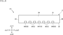
- FIG. 8 is a right side view showing the semiconductor device according to the first embodiment of the present disclosure.
- FIG. 1 is a perspective view showing a semiconductor device according to a first embodiment of the present disclosure.
- FIG. 2 is a perspective view showing the semiconductor device according to the first embodiment of the present disclosure.
- FIG. 3 is a partial perspective
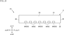
- FIG. 9 is a left side view showing the semiconductor device according to the first embodiment of the present disclosure.
- FIG. 10 is a cross-sectional view taken along line XX in FIG.
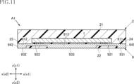
- FIG. 11 is a cross-sectional view taken along line XI-XI in FIG.
- FIG. 12 is a cross-sectional view taken along line XII-XII in FIG.
- FIG. 13 is a partial enlarged plan view showing the semiconductor device according to the first embodiment of the present disclosure.
- FIG. 14 is a partial enlarged plan view showing the semiconductor device according to the first embodiment of the present disclosure.
- FIG. 15 is a partial enlarged plan view showing the semiconductor device according to the first embodiment of the present disclosure.
- FIG. 16 is a partial enlarged plan view showing the semiconductor device according to the first embodiment of the present disclosure.
- FIG. 17 is a bottom view showing a first modified example of the semiconductor device according to the first embodiment of the present disclosure.
- FIG. 18 is a bottom view showing the semiconductor device according to the second embodiment of the present disclosure.
- FIG. 19 is a bottom view showing a semiconductor device according to a third embodiment of the present disclosure.
- FIG. 20 is a bottom view showing the semiconductor device according to the fourth embodiment of the present disclosure.
- FIG. 21 is a partial enlarged plan view showing a second modified example of the semiconductor device according to the first embodiment of the present disclosure.
- FIG. 22 is a partial enlarged plan view showing a third modified example of the semiconductor device according to the first embodiment of the present disclosure.
- FIG. 23 is a plan view showing a semiconductor device according to a fifth embodiment of the present disclosure.
- an object A is formed on an object B" and “an object A is formed on an object B” include “an object A is formed directly on an object B” and “an object A is formed on an object B with another object interposed between the object A and the object B” unless otherwise specified.
- an object A is disposed on an object B” and “an object A is disposed on an object B” include “an object A is disposed directly on an object B” and “an object A is disposed on an object B with another object interposed between the object A and the object B" unless otherwise specified.
- an object A is located on an object B includes “an object A is located on an object B in contact with an object B” and “an object A is located on an object B with another object interposed between the object A and the object B” unless otherwise specified.
- an object A overlaps an object B when viewed in a certain direction includes “an object A overlaps the entire object B” and “an object A overlaps a part of an object B.”
- a surface A faces (one side or the other side of) direction B” is not limited to the case where the angle of surface A with respect to direction B is 90 degrees, but also includes the case where surface A is tilted with respect to direction B.
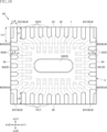
- First embodiment: 1 to 16 show a semiconductor device according to a first embodiment of the present disclosure.
- the semiconductor device A1 of this embodiment includes a semiconductor element 1, a sealing resin 2, and a plurality of leads 4 to 9.
- the semiconductor device A1 is a so-called QFN (Quad Flat No leaded package) type semiconductor device, but the basic configuration of the semiconductor device according to the present disclosure is not limited thereto.
- FIG. 1 is a perspective view showing the semiconductor device A1.
- FIG. 2 is a perspective view showing the semiconductor device A1.
- FIG. 3 is a partial perspective view showing the semiconductor device A1.
- FIG. 4 is a plan view showing the semiconductor device A1.
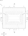
- FIG. 5 is a bottom view showing the semiconductor device A1.
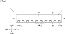
- FIG. 6 is a front view showing the semiconductor device A1.
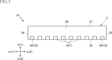
- FIG. 7 is a rear view showing the semiconductor device A1.
- FIG. 8 is a right side view showing the semiconductor device A1.
- FIG. 9 is a left side view showing the semiconductor device A1.
- FIG. 10 is a cross-sectional view taken along line X-X in FIG. 4.
- FIG. 11 is a cross-sectional view taken along line XI-XI in FIG. 4.
- FIG. 10 is a cross-sectional view taken along line X-X in FIG. 4.
- FIG. 12 is a cross-sectional view taken along line XII-XII in FIG. 4.
- FIG. 13 is a partial enlarged plan view showing the semiconductor device A1.
- FIG. 14 is a partial enlarged plan view showing the semiconductor device A1.
- FIG. 15 is a partial enlarged plan view showing the semiconductor device A1.
- FIG. 16 is a partial enlarged plan view showing the semiconductor device A1.
- thickness direction z an example of a thickness direction in this disclosure is indicated as thickness direction z.
- a direction perpendicular to thickness direction z is designated as first direction x.
- a direction perpendicular to thickness direction z and first direction x is designated as second direction y.
- the semiconductor element 1 performs the main electrical function of the semiconductor device A1 when the semiconductor device A1 is mounted on a circuit board or the like to form part of an electrical circuit.
- the specific configuration of the semiconductor element 1 is not limited in any way, and includes an LSI (Large Scale Integration), an IC (Integrated Circuit), and the like.
- the semiconductor element 1 of this embodiment is rectangular in shape with two sides along the first direction x and two sides along the second direction y when viewed in the z direction.
- the sealing resin 2 covers the semiconductor element 1 and a portion of each of the leads 4 to 9.
- the specific configuration of the sealing resin 2 is not limited, and the constituent material thereof includes, for example, epoxy resin.
- the sealing resin 2 of this embodiment has a resin main surface 21, a resin back surface 22, a first resin side surface 23, a second resin side surface 24, a third resin side surface 25, and a fourth resin side surface 26.
- the resin main surface 21 faces the z1 side in the z direction, and in the illustrated example, is a flat rectangular surface.
- the resin back surface 22 faces the z2 side in the z direction, and in the illustrated example, is a flat rectangular surface.
- the first resin side surface 23 is a surface along the first direction x and z directions, and faces the y1 side in the second direction y.
- the second resin side surface 24 is a surface along the second direction y and z directions, and faces the x1 side in the first direction x.
- the third resin side surface 25 is a surface along the second direction y and z directions, and faces the x2 side in the first direction x.
- the fourth resin side surface 26 is a surface along the first direction x and z directions, and faces the y2 side in the second direction y.
- the length in the first direction x of the first resin side surface 23 and the fourth resin side surface 26 is longer than the length in the second direction y of the second resin side surface 24 and the third resin side surface 25.
- the multiple leads 4-9 perform functions such as supporting the semiconductor element 1 and forming a conductive path to the semiconductor element 1.
- the specific configuration of the multiple leads 4-9 is not limited in any way.
- the multiple leads 4-9 may include, as constituent materials, for example, Cu (copper), Ni (nickel), Fe (iron), and alloys thereof.
- the multiple leads 4-9 will be distinguished and explained as multiple first leads 4, multiple second leads 5, multiple third leads 6, multiple fourth leads 7, multiple corner leads 8, and center lead 9.
- the multiple first leads 4 are arranged in a first direction x as shown in Figures 1 to 6 and 12 to 14.
- the first lead 4 has a first thick portion 41, a second thin portion 42, a first mounting surface 43, and a first end surface 44.
- the first thick portion 41 is a portion of the first lead 4 that is relatively thicker in the thickness direction z (compared to the second thin portion 42).
- the first thick portion 41 has a first mounting surface 43 and a first end surface 44.
- the second thin portion 42 is a portion of the first lead 4 that is relatively thinner in the thickness direction z (compared to the first thick portion 41), and is spaced from the resin back surface 22 on the z1 side in the thickness direction z.
- the semiconductor element 1 is mounted on the second thin portion 42.
- the shape of the second thin portion 42 as viewed in the thickness direction z is set appropriately depending on, for example, the position at which the semiconductor element 1 is mounted.
- the first mounting surface 43 faces the z2 side in the thickness direction z, and is exposed from the resin back surface 22 of the sealing resin 2.
- the first mounting surface 43 has a shape that extends along the second direction y.
- the first mounting surface 43 is flush with the resin back surface 22.
- the first mounting surface 43 reaches the first resin side surface 23, and is separated from the second resin side surface 24, the third resin side surface 25, and the fourth resin side surface 26.
- the first end surface 44 faces the y1 side in the second direction y, and is exposed from the first resin side surface 23 of the sealing resin 2.
- the first mounting surface 43 and the first end surface 44 are connected.
- a concave surface or the like may be interposed between the first mounting surface 43 and the first end surface 44.
- a plating layer (not illustrated) containing, for example, Sn (tin) or the like may be appropriately provided on the first mounting surface 43 and the first end surface 44.
- the first end surface 44 is flush with the first resin side surface 23.
- the arrangement pitch P1 of the first mounting surfaces 43 of the multiple first leads 4 is not particularly limited. In the illustrated example, the arrangement pitch P1 of the multiple first mounting surfaces 43 is constant. Furthermore, the width W1, which is the size of the first mounting surfaces 43 in the first direction x, is not particularly limited. In the illustrated example, the width W1 of the multiple first mounting surfaces 43 is constant.
- the first length L1 which is the length of the multiple first leads 4 in the second direction y, of the multiple first leads 4, the first length L1 of the first leads 4 located at both ends in the first direction x is longer than the first length L1 of any of the remaining first leads 4.
- the first length L1 of the first lead 4 sandwiched between two first leads 4 located at both ends in the first direction x is shorter than the first length L1 of the first leads 4 at both ends in the first direction x.
- the first length L1 of the multiple first leads 4 is such that the first length L1 of the first leads 4 located on the outside of the first direction x is longer than the first length L1 of the first leads 4 located toward the center in the first direction x.
- the first length L1 of the first leads 4 located on the outside of the first direction x is longer than the first length L1 of the first leads 4 located on the inside of the first direction x.
- 2nd Lead 5 The multiple second leads 5 are arranged in the first direction x, as shown in Figures 2 to 5, 8, 10, 13, and 15.
- the second lead 5 has a second thick portion 51, a second thin portion 52, a second mounting surface 53, and a second end surface 54.
- the second thick portion 51 is a portion of the second lead 5 that is relatively thicker in the thickness direction z (compared to the second thin portion 52).
- the second thick portion 51 has a second mounting surface 53 and a second end surface 54.
- the second thin portion 52 is a portion of the second lead 5 that is relatively thinner in the thickness direction z (compared to the second thick portion 51), and is spaced from the resin back surface 22 on the z1 side in the thickness direction z.
- the semiconductor element 1 is mounted on the second thin portion 52.
- the shape of the second thin portion 52 as viewed in the thickness direction z is set appropriately depending on, for example, the position at which the semiconductor element 1 is mounted.
- the second mounting surface 53 faces the z2 side in the thickness direction z, and is exposed from the resin back surface 22 of the sealing resin 2.
- the second mounting surface 53 has a shape that extends along the first direction x.
- the second mounting surface 53 is flush with the resin back surface 22.
- the second mounting surface 53 reaches the second resin side surface 24, and is separated from the first resin side surface 23, the fourth resin side surface 26, and the third resin side surface 25.
- the second end surface 54 faces the x1 side of the first direction x and is exposed from the second resin side surface 24 of the sealing resin 2.
- the second mounting surface 53 and the second end surface 54 are connected.
- a concave surface or the like may be interposed between the second mounting surface 53 and the second end surface 54.
- a plating layer (not illustrated) containing, for example, Sn (tin) or the like may be appropriately provided on the second mounting surface 53 and the second end surface 54.
- the second end surface 54 is flush with the second resin side surface 24.
- the arrangement pitch P2 of the second mounting surfaces 53 of the multiple second leads 5 is not particularly limited.
- two second leads 5 are arranged in the second direction y, with the center lead 9 sandwiched between them.
- the arrangement pitch P2 of the two second mounting surfaces 53 on the y1 side of the second direction y is the same as the arrangement pitch P2 of the two second mounting surfaces 53 on the y2 side of the second direction y.
- the width W2, which is the size of the second mounting surfaces 53 in the second direction y is not particularly limited. In the illustrated example, the width W2 of the multiple second mounting surfaces 53 is constant.
- the second length L2 which is the length of the multiple second leads 5 in the second direction y, is not limited in any way and is, for example, constant in this embodiment. Also, in the illustrated example, the second length L2 of the multiple second leads 5 is shorter than the first length L1 of any of the first leads 4.
- the multiple third leads 6 are arranged in the first direction x, as shown in Figures 2 to 5, 8, 10, 13, and 15.
- the third lead 6 has a third thick portion 61, a third thin portion 62, a third mounting surface 63, and a third end surface 64.
- the third thick portion 61 is a portion of the third lead 6 that is relatively thicker in the thickness direction z (compared to the third thin portion 62).
- the third thick portion 61 has a third mounting surface 63 and a third end surface 64.
- the third thin portion 62 is a portion of the third lead 6 that is relatively thinner in the thickness direction z (compared to the third thick portion 61), and is spaced from the resin back surface 22 on the z1 side in the thickness direction z.
- the semiconductor element 1 is mounted on the third thin portion 62.
- the shape of the third thin portion 62 as viewed in the thickness direction z is set appropriately depending on, for example, the position at which the semiconductor element 1 is mounted.
- the third mounting surface 63 faces the z2 side in the thickness direction z, and is exposed from the resin back surface 22 of the sealing resin 2.
- the third mounting surface 63 has a shape extending along the first direction x.
- the third mounting surface 63 is flush with the resin back surface 22.
- the third mounting surface 63 reaches the third resin side surface 25, and is separated from the first resin side surface 23, the fourth resin side surface 26, and the second resin side surface 24.
- the third end surface 64 faces the x2 side of the first direction x and is exposed from the third resin side surface 25 of the sealing resin 2.
- the third mounting surface 63 and the third end surface 64 are connected.
- a concave surface or the like may be interposed between the third mounting surface 63 and the third end surface 64.
- a plating layer (not illustrated) containing, for example, Sn (tin) or the like may be appropriately provided on the third mounting surface 63 and the third end surface 64.
- the third end surface 64 is flush with the third resin side surface 25.
- the arrangement pitch P3 of the third mounting surfaces 63 of the multiple third leads 6 is not particularly limited.
- two third leads 6 are arranged in the second direction y, with the center lead 9 sandwiched between them.
- the arrangement pitch P3 of the two third mounting surfaces 63 on the y1 side of the second direction y is the same as the arrangement pitch P3 of the two third mounting surfaces 63 on the y2 side of the second direction y.
- the width W3, which is the size of the third mounting surfaces 63 in the second direction y is not particularly limited. In the illustrated example, the width W3 of the multiple third mounting surfaces 63 is constant.
- the third length L3, which is the length of the multiple third leads 6 in the second direction y, is not limited in any way and is, for example, constant in this embodiment. In the illustrated example, the third length L3 of the multiple third leads 6 is shorter than the first length L1 of any of the first leads 4.
- the multiple fourth leads 7 are arranged in the first direction x, as shown in Figures 2 to 5, 7, 12, 15, and 16.
- the fourth lead 7 has a fourth thick portion 71, a fourth thin portion 72, a fourth mounting surface 73, and a fourth end surface 74.
- the fourth thick portion 71 is a portion of the fourth lead 7 that is relatively thicker in the thickness direction z (compared to the fourth thin portion 72).
- the fourth thick portion 71 has a fourth mounting surface 73 and a fourth end surface 74.
- the fourth thin portion 72 is a portion of the fourth lead 7 that is relatively thinner in the thickness direction z (compared to the fourth thick portion 71), and is spaced from the resin back surface 22 on the z1 side in the thickness direction z.
- the semiconductor element 1 is mounted on the fourth thin portion 72.
- the shape of the fourth thin portion 72 as viewed in the thickness direction z is set appropriately depending on, for example, the position at which the semiconductor element 1 is mounted.
- the fourth mounting surface 73 faces the z2 side in the thickness direction z, and is exposed from the resin back surface 22 of the sealing resin 2.
- the fourth mounting surface 73 has a shape that extends along the second direction y.
- the fourth mounting surface 73 is flush with the resin back surface 22.
- the fourth mounting surface 73 reaches the fourth resin side surface 26, and is separated from the second resin side surface 24, the third resin side surface 25, and the first resin side surface 23.
- the fourth end surface 74 faces the y2 side in the second direction y and is exposed from the fourth resin side surface 26 of the sealing resin 2.
- the fourth mounting surface 73 and the fourth end surface 74 are connected.
- a concave surface or the like may be interposed between the fourth mounting surface 73 and the fourth end surface 74.
- a plating layer (not illustrated) containing, for example, Sn (tin) or the like may be appropriately provided on the fourth mounting surface 73 and the fourth end surface 74.
- the fourth end surface 74 is flush with the fourth resin side surface 26.
- the arrangement pitch P4 of the fourth mounting surfaces 73 of the multiple fourth leads 7 is not particularly limited. In the illustrated example, the arrangement pitch P4 of the multiple fourth mounting surfaces 73 is constant. Furthermore, the width W4, which is the size of the fourth mounting surfaces 73 in the first direction x, is not particularly limited. In the illustrated example, the width W4 of the multiple fourth mounting surfaces 73 is constant.
- the fourth length L4 which is the length of the multiple fourth leads 7 in the second direction y, of the multiple fourth leads 7 located at both ends in the first direction x is longer than the fourth length L4 of any of the remaining fourth leads 7.
- the fourth length L4 of the fourth lead 7 sandwiched between two fourth leads 7 located at both ends in the first direction x is shorter than the fourth length L4 of the fourth leads 7 at both ends in the first direction x.
- the fourth length L4 of the multiple fourth leads 7 is such that the fourth length L4 of the fourth leads 7 located on the outer side of the first direction x is longer than the fourth length L4 of the fourth leads 7 located toward the center in the first direction x.
- the fourth length L4 of the fourth leads 7 located on the outer side of the first direction x is longer than the fourth length L4 of the fourth leads 7 located on the inner side of the first direction x.
- the first length L1 and the fourth length L4 of the multiple first leads 4 and multiple fourth leads 7 that are located at the same positions in the first direction x are equal to each other.
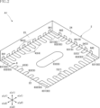
- Corner lead 8 1 to 9 and 13 to 16, the multiple corner leads 8 are arranged in positions close to the four corners as viewed in the thickness direction z of the sealing resin 2. Two corner leads 8 are arranged on both sides in the first direction x of the multiple first leads 4. The other two corner leads 8 are arranged on both sides in the first direction x of the multiple fourth leads 7.
- the corner lead 8 has a thick corner portion 81, a thin corner portion 82, a corner mounting surface 83, a first corner end face 841, and a second corner end face 842.
- the corner thick portion 81 is a portion of the corner lead 8 that is relatively thicker in the thickness direction z (compared to the corner thin portion 82).
- the corner thick portion 81 has a corner mounting surface 83, a first corner end face 841, and a second corner end face 842.
- the corner thin portion 82 is a portion of the corner lead 8 that is relatively thinner in the thickness direction z (compared to the corner thick portion 81), and is spaced from the resin back surface 22 on the z1 side in the thickness direction z.
- the semiconductor element 1 is mounted in the corner thin portion 82.
- the shape of the corner thin portion 82 as viewed in the thickness direction z is set appropriately depending on, for example, the position at which the semiconductor element 1 is mounted.
- the corner mounting surface 83 faces the z2 side in the thickness direction z and is exposed from the resin back surface 22 of the sealing resin 2.
- the corner mounting surface 83 has a first portion 831 and a second portion 832.
- the first portion 831 reaches the first resin side surface 23 or the fourth resin side surface 26 and is separated from the second resin side surface 24 and the third resin side surface 25.
- the second portion 832 reaches the second resin side surface 24 or the third resin side surface 25 and is separated from the first resin side surface 23 and the fourth resin side surface 26.
- the first portion 831 and the second portion 832 are connected at their ends.
- the corner mounting surface 83 is L-shaped when viewed in the thickness direction z.
- the length Lc1 which is the length of the corner mounting surface 83 in the second direction y, is longer than the length Lc2, which is the length in the first direction x.
- the shape and size of the corner mounting surface 83 are not limited in any way.
- the first corner end face 841 faces in the second direction y and is exposed from the first resin side face 23 or the fourth resin side face 26. In the illustrated example, the first corner end face 841 is flush with the first resin side face 23 or the fourth resin side face 26.
- the second corner end face 842 faces in the first direction x and is exposed from the second resin side face 24 or the third resin side face 25. In the illustrated example, the second corner end face 842 is flush with the second resin side face 24 or the third resin side face 25.
- the length Lc1 of the corner mounting surface 83 in the second direction y is greater than the first length L1 of the multiple first leads 4. Also, the length Lc2 of the corner mounting surface 83 in the first direction x is equal to the second length L2 of the multiple second leads 5.
- the arrangement pitch Pc1 between the first mounting surface 43 and the first portion 831 of the first lead 4 located closest to the x1 side in the first direction x is equal to the arrangement pitch Pc1 of the first mounting surfaces 43 of the multiple first leads 4.
- the arrangement pitch Pc2 between the second mounting surface 53 and the second portion 832 of the second lead 5 located closest to the y1 side in the second direction y is equal to the arrangement pitch P2 of the second mounting surfaces 53 of the multiple second leads 5.
- the length Lc1 of the corner mounting surface 83 in the second direction y is greater than the first length L1 of the multiple first leads 4. Also, the length Lc2 of the corner mounting surface 83 in the first direction x is equal to the third length L3 of the multiple third leads 6.
- the arrangement pitch Pc1 between the first mounting surface 43 and the first portion 831 of the first lead 4 located closest to the x2 side in the first direction x is equal to the arrangement pitch Pc1 of the first mounting surfaces 43 of the multiple first leads 4.
- the arrangement pitch Pc3 between the third mounting surface 63 and the second portion 832 of the third lead 6 located closest to the y1 side in the second direction y is equal to the arrangement pitch P2 of the third mounting surfaces 63 of the multiple third leads 6.
- the length Lc1 of the corner mounting surface 83 in the second direction y is greater than the fourth length L4 of the multiple fourth leads 7.
- the length Lc2 of the corner mounting surface 83 in the first direction x is equal to the second length L2 of the multiple second leads 5.
- the arrangement pitch Pc4 between the fourth mounting surface 73 and the first portion 831 of the fourth lead 7 located closest to the x1 side in the first direction x is equal to the arrangement pitch P4 of the fourth mounting surfaces 73 of the multiple fourth leads 7.
- the arrangement pitch Pc3 between the third mounting surface 63 and the second portion 832 of the third lead 6 located closest to the y2 side in the second direction y is equal to the arrangement pitch P3 of the third mounting surfaces 63 of the multiple third leads 6.
- the length Lc1 of the corner mounting surface 83 in the second direction y is greater than the fourth length L4 of the multiple fourth leads 7. Also, the length Lc2 of the corner mounting surface 83 in the first direction x is equal to the third length L3 of the multiple third leads 6.
- the arrangement pitch Pc4 between the fourth mounting surface 73 and the first portion 831 of the fourth lead 7 located furthest on the x2 side in the first direction x is equal to the arrangement pitch P4 of the fourth mounting surfaces 73 of the multiple fourth leads 7.
- the arrangement pitch Pc2 between the second mounting surface 53 and the second portion 832 of the second lead 5 located furthest on the y2 side in the second direction y is equal to the arrangement pitch P2 of the second mounting surfaces 53 of the multiple second leads 5.
- Center lead 9 The center lead 9 is disposed between the second leads 5 or between the third leads 6 in the second direction y, as shown in Figures 1 to 5, 8, 9, 11 and 12. In the illustrated example, the center lead 9 overlaps with the center of the semiconductor device A1 (sealing resin 2) in the second direction y. In the illustrated example, the center lead 9 has a center thick portion 911, a center thick portion 912, a center thick portion 913, a center thin portion 921, a center thin portion 922, a center mounting surface 931, a center mounting surface 932, a center mounting surface 933, a center end surface 941 and a center end surface 942.
- the center mounting surface 931, center mounting surface 932, and center mounting surface 933 are portions of the center lead 9 that are relatively thick in the thickness direction z (compared to the center thin portion 921 and center thin portion 922).
- the center thick portion 911 has a center mounting surface 931 and a center end surface 941
- the center thick portion 912 has a center mounting surface 932 and a center end surface 942
- the center thick portion 913 has a center mounting surface 933.
- the center thick portion 911 is disposed on the x1 side of the first direction x
- the center thick portion 912 is disposed on the x2 side of the first direction x
- the center thick portion 913 is disposed in the center of the first direction x.
- the center thin portion 921 and the center thin portion 922 are portions of the center lead 9 that are relatively thin in the thickness direction z (compared to the center thick portion 911, the center thick portion 912, and the center thick portion 913), and are spaced apart from the resin back surface 22 on the z1 side in the thickness direction z.
- the semiconductor element 1 is mounted on the center thin portion 921 and the center thin portion 922.
- the length in the first direction x of the center mounting surface 931 is equal to the second length L2 of the second mounting surface 53 of the second lead 5. Furthermore, the length in the first direction x of the center mounting surface 932 is equal to the third length L3 of the third mounting surface 63 of the third lead 6.
- the arrangement pitch between the center mounting surface 931 and the second mounting surface 53 adjacent thereto in the second direction y is equal to the arrangement pitch P2 of the multiple second mounting surfaces 53. Furthermore, the arrangement pitch between the center mounting surface 932 and the third mounting surface 63 adjacent thereto in the second direction y is equal to the arrangement pitch P3 of the multiple third mounting surfaces 63.
- the first mounting surfaces 43 of the leads 4 are conductively joined to the circuit board or the like by a conductive bonding material such as solder.
- each mounting surface of the leads 5 to 9 is conductively joined to the circuit board or the like by a conductive bonding material.
- thermal stress or the like may occur in these conductive bonding materials.
- the first length L1 which is the length of the multiple first leads 4 in the second direction y, of the multiple first leads 4 located at both ends in the first direction x is longer than the first length L1 of any of the remaining first leads 4.
- the first length L1 of the first lead 4 sandwiched between two first leads 4 located at both ends in the first direction x is shorter than the first length L1 of the first leads 4 at both ends in the first direction x.
- the first length L1 of the multiple first leads 4 is longer for the first lead 4 located on the outside of the first direction x than for the first lead 4 located toward the center in the first direction x.
- the first length L1 of the first lead 4 located on the outside of the first direction x is longer than the first length L1 of the first lead 4 located on the inside of the first direction x.
- the fourth length L4 which is the length in the second direction y of the multiple fourth leads 7, of the multiple fourth leads 7 located at both ends in the first direction x is longer than the fourth length L4 of any of the remaining fourth leads 7.
- the fourth length L4 of the fourth lead 7 sandwiched between two fourth leads 7 located at both ends in the first direction x is shorter than the fourth length L4 of the fourth leads 7 at both ends in the first direction x.
- the fourth length L4 of the multiple fourth leads 7 is such that the fourth length L4 of the fourth lead 7 located on the outer side of the first direction x is longer than the fourth length L4 of the fourth lead 7 located toward the center in the first direction x.
- the fourth length L4 of the fourth lead 7 located on the outer side of the first direction x is longer than the fourth length L4 of the fourth lead 7 located on the inner side of the first direction x.
- the corner mounting surface 83 has a first portion 831 and a second portion 832.
- the first portion 831 reaches the first resin side surface 23 or the fourth resin side surface 26 and is separated from the second resin side surface 24 and the third resin side surface 25.
- the second portion 832 reaches the second resin side surface 24 or the third resin side surface 25 and is separated from the first resin side surface 23 and the fourth resin side surface 26.
- the first portion 831 and the second portion 832 are connected to each other at their ends. Therefore, the corner mounting surface 83 is configured to be separated from the corner where the first resin side surface 23, the second resin side surface 24, the third resin side surface 25, and the fourth resin side surface 26 are connected to each other. This makes it possible to suppress excessive stress from occurring in the conductive bonding material bonded to the corner mounting surface 83.
- the arrangement pitch Pc1 between the first mounting surface 43 and the first portion 831 of the first lead 4 located furthest to the x1 side in the first direction x is equal to the arrangement pitch P1 of the multiple first mounting surfaces 43.
- This effect is also achieved by the relationship between the arrangement pitch Pc1 and the arrangement pitch P1 in FIG. 14, the relationship between the arrangement pitch Pc4 and the arrangement pitch P4 in FIG. 15, and the relationship between the arrangement pitch Pc4 and the arrangement pitch P4 in FIG. 16.
- the arrangement pitch Pc2 between the second mounting surface 53 of the second lead 5 located furthest to the y1 side in the second direction y and the second portion 832 is equal to the arrangement pitch P2 between the second mounting surfaces 53 of the multiple second leads 5. This makes it possible to prevent excessive stress from being generated in any of the conductive bonding materials bonded to the multiple second mounting surfaces 53 and the second portions 832. This effect is also achieved by the relationship between the arrangement pitch Pc3 and the arrangement pitch P3 in FIG. 14, the relationship between the arrangement pitch Pc2 and the arrangement pitch P2 in FIG. 15, and the relationship between the arrangement pitch Pc3 and the arrangement pitch P3 in FIG. 16.
- the width Wc1 of the first portion 831 is equal to the width W1 of the first mounting surface 43 or the width W4 of the fourth mounting surface 73. Furthermore, the width Wc2 of the second portion 832 is equal to the width W2 of the second mounting surface 53 or the width W3 of the third mounting surface 63. This makes it possible to make the stress generated in the conductive bonding material bonded to these mounting surfaces more uniform.
- FIGS. 17 to 20 show modified examples and other embodiments of the present disclosure.
- elements that are the same as or similar to those in the above-described embodiment are given the same reference numerals as in the above-described embodiment.
- the configurations of the various parts in each modified example and each embodiment can be combined with each other as appropriate to the extent that no technical contradictions arise.
- First Modification of First Embodiment 17 shows a first modified example of the semiconductor device A1.
- the semiconductor device A11 of this modified example differs from the above-described example in the configuration of the plurality of first leads 4 and the plurality of fourth leads 7.
- the first lengths L1 of the multiple first leads 4 are equal except for the first leads 4 located on both sides of the first direction x.
- the first lengths L1 of the multiple first leads 4 located on both sides of the first direction x are longer than the first lengths L1 of the remaining first leads 4.
- the fourth lengths L4 of the multiple fourth leads 7 are equal to each other except for the fourth leads 7 located on both sides of the first direction x.
- the fourth lengths L4 of the multiple fourth leads 7 located on both sides of the first direction x are longer than the fourth lengths L4 of the remaining fourth leads 7.
- This modified example also makes it possible to prevent excessive stress from being generated in the conductive bonding material used for mounting. Furthermore, as can be understood from this modified example, the configuration in which the first length L1 of the first leads 4 located on both sides of the first direction x among the multiple first leads 4 is longer than the first length L1 of the remaining first leads 4 can be modified in various ways. Furthermore, the configuration in which the fourth length L4 of the fourth leads 7 located on both sides of the first direction x among the multiple fourth leads 7 is longer than the fourth length L4 of the remaining fourth leads 7 can be modified in various ways.
- Second embodiment: 18 shows a semiconductor device according to a second embodiment of the present disclosure.
- a semiconductor device A2 of this embodiment differs from the above-described embodiment in the configurations of the multiple second leads 5 and the multiple third leads 6.
- the second length L2 of the second leads 5 located on both sides of the multiple second leads 5 when viewed in the y direction is longer than the second length L2 of the remaining second leads 5.
- the second length L2 of the second lead 5 sandwiched between two second leads 5 located at both ends in the second direction y is shorter than the second length L2 of the second leads 5 at both ends in the second direction y.
- the second length L2 of the multiple second leads 5 is such that the second length L2 of the second leads 5 located on the outer side in the second direction y is longer than the second length L2 of the second leads 5 located toward the center in the second direction y.
- the second length L2 of the second leads 5 located on the outer side in the second direction y is longer than the second length L2 of the second leads 5 located on the inner side in the first direction x.
- This embodiment also makes it possible to prevent excessive stress from being generated in the conductive bonding material used for mounting. Furthermore, in this embodiment, by configuring the second length L2 of the multiple second leads 5 and the third length L3 of the multiple third leads 6 as described above, it is possible to more effectively prevent excessive stress from being generated in the conductive bonding material.
- Third embodiment: 19 shows a semiconductor device according to a third embodiment of the present disclosure.
- the length in the first direction x of the first resin side surface 23 and the fourth resin side surface 26 is shorter than the length in the second direction y of the second resin side surface 24 and the third resin side surface 25.
- the center lead 9 is disposed between the multiple first leads 4 and the multiple fourth leads 7 in the first direction x.
- the semiconductor device A3 can be said to have a configuration similar to that of the semiconductor device A1, rotated 90 degrees in the thickness direction z, with the names and symbols redefined.
- This embodiment also makes it possible to prevent excessive stress from being generated in the conductive bonding material used for mounting. Furthermore, as can be seen from this embodiment, when the sealing resin 2 is rectangular when viewed in the thickness direction z, a configuration can be appropriately adopted in which the length of the leads at both ends is increased on either or both of the short and long sides.
- Fourth embodiment 20 shows a semiconductor device according to a fourth embodiment of the present disclosure.
- a semiconductor device A4 of this embodiment differs from the above-described embodiments in the configuration of the corner leads 8.
- the corner mounting surface 83 of the corner lead 8 is pentagonal with one corner of the rectangle chamfered.
- the size of the corner mounting surface 83 in the second direction y is smaller than the first length L1 and the fourth length L4, and the size of the corner mounting surface 83 in the first direction x is smaller than the second length L2 and the third length L3.
- the second mounting surface 53 and the third mounting surface 63 located closest to the y1 side in the second direction y overlap with the first mounting surface 43 located on both sides in the first direction x when viewed in the first direction x.
- the second mounting surface 53 and the third mounting surface 63 located closest to the y2 side in the second direction y overlap with the fourth mounting surface 73 located on both sides in the first direction x when viewed in the first direction x.
- This embodiment also makes it possible to prevent excessive stress from being generated in the conductive bonding material used for mounting. Furthermore, as can be understood from this embodiment, the configuration of the corner leads 8 is not limited in any way and can be set appropriately. Furthermore, the semiconductor device disclosed herein may be configured without including corner leads 8.
- the semiconductor device of the present disclosure is not limited to the above-mentioned embodiments 1 to 4 and the above-mentioned modified examples.
- Figures 21 to 23 show other modified examples and embodiments of the present disclosure.
- elements that are the same as or similar to those in the modified examples and embodiments are given the same reference numerals as those in the modified examples and embodiments.
- the configurations of the parts in each modified example and each embodiment can be combined with each other as appropriate to the extent that no technical contradiction occurs.
- Second Modification of First Embodiment 21 shows a second modification of the semiconductor device A1.
- the configuration of the corner leads 8 is different from that of the example described above (see FIG. 14).
- the length Lc1 and the length Lc2 of the corner mounting surface 83 are equal to each other.
- the sealing resin 2 may be, for example, square-shaped when viewed in the thickness direction z.
- This modified example also makes it possible to prevent excessive stress from being generated in the conductive bonding material used for mounting. Furthermore, as can be seen from this modified example, there are no limitations on the specific shape, etc., of the corner mounting surface 83.
- Third Modification of First Embodiment 22 shows a third modification of the semiconductor device A1.
- the semiconductor device A13 of this modification has a different configuration of the corner leads 8 from the above-mentioned examples.
- the corner mounting surface 83 has a first portion 831, a second portion 832, and a third portion 833.
- the third portion 833 is located between the second portion 832 and the first resin side surface 23 or the fourth resin side surface 26 in the second direction y, and reaches the first portion 831 and the second resin side surface 24 or the third resin side surface 25.
- the corner mounting surface 83 has the first portion 831, the second portion 832, and the third portion 833, and is therefore F-shaped when viewed in the thickness direction z.
- the third portion 833 is located between the second portion 832 and the first resin side surface 23 in the second direction y, and reaches the first portion 831 and the third resin side surface 25.
- the arrangement pitch between the second portions 832 may be the same as the arrangement pitch P2 or the arrangement pitch P3 in the above-mentioned example.
- the width in the second direction y of the second portion 832 and the third portion 833 may be the same as the width W2 or the width W3 in the above-mentioned example.
- This modified example also prevents excessive stress from being generated in the conductive bonding material used for mounting.
- the specific shape of the corner mounting surface 83 is not limited in any way as long as it is spaced apart from the four corners of the sealing resin 2.
- Fifth embodiment: 23 shows a semiconductor device according to a fifth embodiment of the present disclosure.
- a semiconductor device A5 of this embodiment differs from the above-described embodiments in the configurations of the multiple first leads 4 and the multiple fourth leads 7.
- the first lengths L1 of the multiple first leads 4 are all equal. Furthermore, the length Lc1 of the corner lead 8 is longer than the first length L1 of the multiple first leads 4. Similarly, the fourth lengths L4 of the multiple fourth leads 7 are all equal. Furthermore, the length Lc1 of the corner lead 8 is longer than the fourth length L4 of the multiple fourth leads 7.
- first length L1 of the first leads 4, the fourth length L4 of the fourth leads 7, the second length L2 of the second leads 5, and the third length L3 of the third leads 6 may have any length relationship.
- the semiconductor device according to the present disclosure is not limited to the above-mentioned embodiment and modifications.
- the specific configuration of each part of the semiconductor device according to the present disclosure can be freely designed in various ways.
- the present disclosure includes the embodiments described in the following appendix.
- Appendix 1A A semiconductor element; Multiple leads and a sealing resin that covers the semiconductor element and at least a portion of each of the plurality of leads, the sealing resin has a resin back surface facing a thickness direction of the semiconductor element, a first resin side surface along a first direction intersecting the thickness direction, and a second resin side surface and a third resin side surface along a second direction intersecting the thickness direction and the first direction; the plurality of leads includes a plurality of first leads arranged in the first direction; Each of the first leads has a first mounting surface exposed from the resin back surface, the first mounting surface reaches the first resin side surface and is spaced apart from the second resin side surface and the third resin side surface, A semiconductor device, wherein a first length, which is the length in the second direction of the first mounting surface of the plurality of first leads, of the plurality of first leads located at both ends in the first direction is longer than the first length of any of the remaining first leads.
- Appendix 2A The semiconductor device of Appendix 1A, wherein the first length of the plurality of first leads is longer for those located on the outer side in the first direction than for those located on the central side in the first direction.
- Appendix 3A The semiconductor device according to claim 1A or 2A, wherein the sealing resin has a rectangular shape when viewed in the thickness direction.
- Appendix 4A The semiconductor device according to any one of claims 1A to 3A, wherein the plurality of first leads have first end faces exposed from a side surface of the first resin.
- Appendix 5A The semiconductor device according to any one of claims 1A to 4A, wherein the first mounting surface has a shape extending along the second direction.
- Appendix 6A The semiconductor device of Appendix 1A, wherein the first length of the plurality of first leads is longer for those located on the outer side in the first direction than for those located on the central side in the first direction.
- Appendix 3A The semiconductor device according to claim 1A or 2A, wherein the sealing resin has
- the sealing resin further has a fourth resin side surface facing an opposite side to the first resin side surface in the second direction
- the multiple leads further include a multiple second leads arranged in the second direction along the second resin side surface, a multiple third leads arranged in the second direction along the third resin side surface, and a multiple fourth leads arranged in the first direction along the fourth resin side surface.
- Appendix 11A Appendix 11A.
- Each of the second leads has a second mounting surface exposed from the resin back surface, the second mounting surface reaches the second resin side surface and is spaced apart from the first resin side surface and the fourth resin side surface, each of the third leads has a third mounting surface exposed from the resin back surface; the third mounting surface reaches the third resin side surface and is spaced apart from the first resin side surface and the fourth resin side surface, each of the plurality of fourth leads has a fourth mounting surface exposed from the resin back surface;
- the semiconductor device according to claim 10A wherein the fourth mounting surface reaches the fourth resin side surface and is spaced apart from the second resin side surface and the third resin side surface. Appendix 12A.
- Appendix 15A
- a second length which is a length in the first direction of the second mounting surfaces of the plurality of second leads, the second lengths of the second leads located at both ends in the second direction among the plurality of second leads are longer than the second lengths of any of the remaining second leads;
- Appendix 16A Appendix 16A.
- the plurality of leads further include a corner lead having a corner mounting surface exposed from the resin back surface on an outer side in the first direction with respect to the first mounting surfaces of the plurality of first leads, the corner mounting surface has a first portion that reaches the first resin side surface and is separated from the second resin side surface and the third resin side surface, and a second portion that reaches the second resin side surface or the third resin side surface and is separated from the first resin side surface and the fourth resin side surface,
- the semiconductor device according to any one of appendices 11A to 15A, wherein the first portion and the second portion are connected to each other.
- Appendix 17A The semiconductor device according to claim 16A, wherein a length in the second direction of the corner mounting surface is longer than the first lengths of the first leads located at both ends in the first direction among the plurality of first leads.
- Appendix 1B A semiconductor element; Multiple leads and a sealing resin that covers the semiconductor element and at least a portion of each of the plurality of leads, the sealing resin has a resin back surface facing a thickness direction of the semiconductor element, a first resin side surface and a fourth resin side surface along a first direction intersecting the thickness direction, and a second resin side surface and a third resin side surface along a second direction intersecting the thickness direction and the first direction, the plurality of leads includes a plurality of first leads, a plurality of fourth leads and a corner lead; the first leads are arranged in the first direction along the first resin side surface, the fourth leads are arranged in the first direction along the fourth resin side surface, Each of the first leads has a first mounting surface exposed from the resin back surface, each of the plurality of fourth leads has a fourth mounting surface exposed from the resin back surface; the corner lead has a corner mounting surface exposed from the resin back surface on an outer side in the first direction with respect to the first mounting surfaces
- Appendix 2B The semiconductor device according to claim 1B, wherein the sealing resin has a rectangular shape when viewed in the thickness direction.
- Appendix 3B The semiconductor device according to claim 1B or 2B, wherein an arrangement pitch of the first mounting surfaces of the plurality of first leads is equal to an arrangement pitch between the first mounting surface and the first portion of the first lead that is located at the outermost side in the first direction among the plurality of first leads.
- Appendix 4B The semiconductor device according to any one of appendices 1B to 3B, wherein a width in the first direction of the first mounting surface of the plurality of first leads is equal to a width in the first direction of the first portion.
- Appendix 5B The semiconductor device according to any one of appendices 1B to 3B, wherein a width in the first direction of the first mounting surface of the plurality of first leads is equal to a width in the first direction of the first portion.
- Appendix 15B A semiconductor device described in any one of Appendix 1B to 13B, wherein the plurality of leads further include a plurality of second leads arranged in the second direction along the second resin side surface, a plurality of third leads arranged in the second direction along the third resin side surface, and a plurality of fourth leads arranged in the first direction along the fourth resin side surface.
- Each of the second leads has a second mounting surface exposed from the resin back surface, the second mounting surface reaches the second resin side surface and is spaced apart from the first resin side surface and the fourth resin side surface, each of the third leads has a third mounting surface exposed from the resin back surface; the third mounting surface reaches the third resin side surface and is spaced apart from the first resin side surface and the fourth resin side surface,
- Appendix 15B wherein an arrangement pitch of the second mounting surfaces of the plurality of second leads and an arrangement pitch between the second mounting surface and the second portion of the second lead that is located outermost in the second direction among the plurality of second leads are equal.
- Appendix 17B The semiconductor device according to claim 15B or 16B, wherein a width of the second mounting surface of the second leads in the second direction is equal to a width of the second portion in the second direction.
Landscapes
- Physics & Mathematics (AREA)
- Condensed Matter Physics & Semiconductors (AREA)
- General Physics & Mathematics (AREA)
- Engineering & Computer Science (AREA)
- Computer Hardware Design (AREA)
- Microelectronics & Electronic Packaging (AREA)
- Power Engineering (AREA)
- Structures Or Materials For Encapsulating Or Coating Semiconductor Devices Or Solid State Devices (AREA)
Abstract
In the present invention, a semiconductor device comprises a semiconductor element, a plurality of leads, and an encapsulating resin that covers the semiconductor element and the plurality of leads. The encapsulating resin has a resin rear surface and first to third resin side surfaces. The plurality of leads include a plurality of first leads that are arranged in a first direction. Each first lead has a first mounting surface that is exposed from the resin rear surface. The first mounting surface reaches the first resin side surface, and is set apart from the second resin side surface and the third resin side surface. The first mounting surface has a first length that follows along a second direction. The first lengths of the first leads among the plurality of first leads that are positioned at both ends in the first direction are longer than the first lengths of the other first leads.
Description
本開示は、半導体装置に関する。
This disclosure relates to a semiconductor device.
特許文献1には、従来の半導体装置の一例が開示されている。同文献に開示された半導体装置は、半導体素子、複数のリードおよび封止樹脂を備える。複数のリードは、封止樹脂の裏面から露出する実装面を有する。これらの実装面は、封止樹脂の側面に沿って配列されている。
Patent Document 1 discloses an example of a conventional semiconductor device. The semiconductor device disclosed in this document comprises a semiconductor element, multiple leads, and sealing resin. The multiple leads have mounting surfaces exposed from the back surface of the sealing resin. These mounting surfaces are arranged along the side surface of the sealing resin.
複数のリードの実装面は、はんだ等の導電性接合材によって回路基板等に接合される。これらの導電性接合材のいずれかに過大な応力が生じると、導電性接合材の亀裂や剥離の原因となる。
The mounting surfaces of the multiple leads are joined to a circuit board or the like by a conductive bonding material such as solder. If excessive stress is applied to any of these conductive bonding materials, it can cause the conductive bonding material to crack or peel off.
本開示は、従来より改良が施された半導体装置を提供することを一の課題とする。特に本開示は、上記した事情に鑑み、実装に用いられる導電性接合材に過大な応力が生じることを抑制可能な半導体装置を提供することを一の課題とする。
An object of the present disclosure is to provide a semiconductor device that is an improvement over conventional semiconductor devices. In particular, in view of the above-mentioned circumstances, an object of the present disclosure is to provide a semiconductor device that can prevent excessive stress from being generated in the conductive bonding material used for mounting.
本開示の第1の側面によって提供される半導体装置は、半導体素子と、複数のリードと、前記半導体素子と前記複数のリードの少なくとも一部ずつとを覆う封止樹脂と、を備える。前記封止樹脂は、前記半導体素子の厚さ方向を向く樹脂裏面と、前記厚さ方向と交差する第1方向に沿う第1樹脂側面と、前記厚さ方向および前記第1方向に交差する第2方向に沿う第2樹脂側面および第3樹脂側面と、を有する。前記複数のリードは、前記第1方向に配列された複数の第1リードを含み、前記複数の第1リードの各々は、前記樹脂裏面から露出する第1実装面を有する。前記第1実装面は、前記第1樹脂側面に到達し、且つ前記第2樹脂側面および前記第3樹脂側面から離隔している。前記複数の第1リードの前記第1実装面の前記第2方向の長さである第1長さは、前記複数の第1リードのうち前記第1方向の両端に位置するものの前記第1長さが、その余のいずれの前記第1リードの前記第1長さよりも長い。
The semiconductor device provided by the first aspect of the present disclosure includes a semiconductor element, a plurality of leads, and a sealing resin covering the semiconductor element and at least a portion of each of the plurality of leads. The sealing resin has a resin back surface facing the thickness direction of the semiconductor element, a first resin side surface along a first direction intersecting the thickness direction, and a second resin side surface and a third resin side surface along a second direction intersecting the thickness direction and the first direction. The plurality of leads include a plurality of first leads arranged in the first direction, and each of the plurality of first leads has a first mounting surface exposed from the resin back surface. The first mounting surface reaches the first resin side surface and is separated from the second resin side surface and the third resin side surface. The first length, which is the length in the second direction of the first mounting surfaces of the plurality of first leads, is longer than the first length of any of the remaining first leads.
本開示の第2の側面によって提供される半導体装置は、半導体素子と、複数のリードと、前記半導体素子と前記複数のリードの少なくとも一部ずつとを覆う封止樹脂と、を備える。前記封止樹脂は、前記半導体素子の厚さ方向を向く樹脂裏面と、前記厚さ方向と交差する第1方向に沿う第1樹脂側面および第4樹脂側面と、前記厚さ方向および前記第1方向に交差する第2方向に沿う第2樹脂側面および第3樹脂側面と、を有する。前記複数のリードは、複数の第1リード、複数の第4リードおよびコーナーリードを含む。前記複数の第1リードは、前記第1樹脂側面に沿って前記第1方向に配列されており、前記複数の第4リードは、前記第4樹脂側面に沿って前記第1方向に配列されている。前記複数の第1リードの各々は、前記樹脂裏面から露出する第1実装面を有する。前記複数の第4リードの各々は、前記樹脂裏面から露出する第4実装面を有する。前記コーナーリードは、前記複数の第1リードの前記第1実装面または前記複数の第4リードの前記第4実装面に対して前記第1方向の外側において前記樹脂裏面から露出するコーナー実装面を有する。前記コーナー実装面は、前記第1樹脂側面または前記第4樹脂側面に到達し且つ前記第2樹脂側面および前記第3樹脂側面から離隔した第1部と、前記第2樹脂側面または前記第3樹脂側面に到達し且つ前記第1樹脂側面および前記第4樹脂側面から離隔した第2部と、を有する。前記第1部と前記第2部とが繋がっている。
A semiconductor device provided by a second aspect of the present disclosure includes a semiconductor element, a plurality of leads, and a sealing resin covering the semiconductor element and at least a portion of each of the plurality of leads. The sealing resin has a resin back surface facing the thickness direction of the semiconductor element, a first resin side surface and a fourth resin side surface along a first direction intersecting the thickness direction, and a second resin side surface and a third resin side surface along a second direction intersecting the thickness direction and the first direction. The plurality of leads include a plurality of first leads, a plurality of fourth leads, and a corner lead. The plurality of first leads are arranged in the first direction along the first resin side surface, and the plurality of fourth leads are arranged in the first direction along the fourth resin side surface. Each of the plurality of first leads has a first mounting surface exposed from the resin back surface. Each of the plurality of fourth leads has a fourth mounting surface exposed from the resin back surface. The corner lead has a corner mounting surface exposed from the resin back surface on the outside of the first direction relative to the first mounting surfaces of the plurality of first leads or the fourth mounting surfaces of the plurality of fourth leads. The corner mounting surface has a first portion that reaches the first resin side surface or the fourth resin side surface and is separated from the second resin side surface and the third resin side surface, and a second portion that reaches the second resin side surface or the third resin side surface and is separated from the first resin side surface and the fourth resin side surface. The first portion and the second portion are connected.
上記構成によれば、半導体装置において、実装に用いられる導電性接合材に過大な応力が生じることを抑制することができる。
The above configuration makes it possible to prevent excessive stress from being generated in the conductive bonding material used in mounting the semiconductor device.
本開示のその他の特徴および利点は、添付図面を参照して以下に行う詳細な説明によって、より明らかとなろう。
Other features and advantages of the present disclosure will become more apparent from the following detailed description taken in conjunction with the accompanying drawings.
以下、本開示の好ましい実施の形態につき、図面を参照して具体的に説明する。
Below, a preferred embodiment of this disclosure will be described in detail with reference to the drawings.
本開示における「第1」、「第2」、「第3」等の用語は、単に識別のために用いたものであり、それらの対象物に順列を付することを意図していない。
Terms such as "first," "second," and "third" in this disclosure are used merely for identification purposes and are not intended to assign any rank to their objects.
本開示において、「ある物Aがある物Bに形成されている」および「ある物Aがある物B上に形成されている」とは、特段の断りのない限り、「ある物Aがある物Bに直接形成されていること」、および、「ある物Aとある物Bとの間に他の物を介在させつつ、ある物Aがある物Bに形成されていること」を含む。同様に、「ある物Aがある物Bに配置されている」および「ある物Aがある物B上に配置されている」とは、特段の断りのない限り、「ある物Aがある物Bに直接配置されていること」、および、「ある物Aとある物Bとの間に他の物を介在させつつ、ある物Aがある物Bに配置されていること」を含む。同様に、「ある物Aがある物B上に位置している」とは、特段の断りのない限り、「ある物Aがある物Bに接して、ある物Aがある物B上に位置していること」、および、「ある物Aとある物Bとの間に他の物が介在しつつ、ある物Aがある物B上に位置していること」を含む。また、「ある物Aがある物Bにある方向に見て重なる」とは、特段の断りのない限り、「ある物Aがある物Bのすべてに重なること」、および、「ある物Aがある物Bの一部に重なること」を含む。また、本開示において「ある面Aが方向B(の一方側または他方側)を向く」とは、面Aの方向Bに対する角度が90°である場合に限定されず、面Aが方向Bに対して傾いている場合を含む。
In this disclosure, "an object A is formed on an object B" and "an object A is formed on an object B" include "an object A is formed directly on an object B" and "an object A is formed on an object B with another object interposed between the object A and the object B" unless otherwise specified. Similarly, "an object A is disposed on an object B" and "an object A is disposed on an object B" include "an object A is disposed directly on an object B" and "an object A is disposed on an object B with another object interposed between the object A and the object B" unless otherwise specified. Similarly, "an object A is located on an object B" includes "an object A is located on an object B in contact with an object B" and "an object A is located on an object B with another object interposed between the object A and the object B" unless otherwise specified. Additionally, unless otherwise specified, "an object A overlaps an object B when viewed in a certain direction" includes "an object A overlaps the entire object B" and "an object A overlaps a part of an object B." Additionally, in this disclosure, "a surface A faces (one side or the other side of) direction B" is not limited to the case where the angle of surface A with respect to direction B is 90 degrees, but also includes the case where surface A is tilted with respect to direction B.
第1実施形態:
図1~図16は、本開示の第1実施形態に係る半導体装置を示している。本実施形態の半導体装置A1は、半導体素子1、封止樹脂2および複数のリード4~9を備える。半導体装置A1は、いわゆるQFN(Quad Flat No leaded package)タイプの半導体装置であるが、本開示の半導体装置の基本構成は、何ら限定されない。 First embodiment:
1 to 16 show a semiconductor device according to a first embodiment of the present disclosure. The semiconductor device A1 of this embodiment includes asemiconductor element 1, a sealing resin 2, and a plurality of leads 4 to 9. The semiconductor device A1 is a so-called QFN (Quad Flat No leaded package) type semiconductor device, but the basic configuration of the semiconductor device according to the present disclosure is not limited thereto.
図1~図16は、本開示の第1実施形態に係る半導体装置を示している。本実施形態の半導体装置A1は、半導体素子1、封止樹脂2および複数のリード4~9を備える。半導体装置A1は、いわゆるQFN(Quad Flat No leaded package)タイプの半導体装置であるが、本開示の半導体装置の基本構成は、何ら限定されない。 First embodiment:
1 to 16 show a semiconductor device according to a first embodiment of the present disclosure. The semiconductor device A1 of this embodiment includes a
図1は、半導体装置A1を示す斜視図である。図2は、半導体装置A1を示す斜視図である。図3は、半導体装置A1を示す部分斜視図である。図4は、半導体装置A1を示す平面図である。図5は、半導体装置A1を示す底面図である。図6は、半導体装置A1を示す正面図である。図7は、半導体装置A1を示す背面図である。図8は、半導体装置A1を示す右側面図である。図9は、半導体装置A1を示す左側面図である。図10は、図4のX-X線に沿う断面図である。図11は、図4のXI-XI線に沿う断面図である。図12は、図4のXII-XII線に沿う断面図である。図13は、半導体装置A1を示す部分拡大平面図である。図14は、半導体装置A1を示す部分拡大平面図である。図15は、半導体装置A1を示す部分拡大平面図である。図16は、半導体装置A1を示す部分拡大平面図である。
FIG. 1 is a perspective view showing the semiconductor device A1. FIG. 2 is a perspective view showing the semiconductor device A1. FIG. 3 is a partial perspective view showing the semiconductor device A1. FIG. 4 is a plan view showing the semiconductor device A1. FIG. 5 is a bottom view showing the semiconductor device A1. FIG. 6 is a front view showing the semiconductor device A1. FIG. 7 is a rear view showing the semiconductor device A1. FIG. 8 is a right side view showing the semiconductor device A1. FIG. 9 is a left side view showing the semiconductor device A1. FIG. 10 is a cross-sectional view taken along line X-X in FIG. 4. FIG. 11 is a cross-sectional view taken along line XI-XI in FIG. 4. FIG. 12 is a cross-sectional view taken along line XII-XII in FIG. 4. FIG. 13 is a partial enlarged plan view showing the semiconductor device A1. FIG. 14 is a partial enlarged plan view showing the semiconductor device A1. FIG. 15 is a partial enlarged plan view showing the semiconductor device A1. FIG. 16 is a partial enlarged plan view showing the semiconductor device A1.
これらの図において、本開示の厚さ方向の一例を厚さ方向zと表記している。厚さ方向zと直交する一方向を第1方向xとする。厚さ方向zおよび第1方向xと直交する方向を第2方向yとする。
In these figures, an example of a thickness direction in this disclosure is indicated as thickness direction z. A direction perpendicular to thickness direction z is designated as first direction x. A direction perpendicular to thickness direction z and first direction x is designated as second direction y.
半導体素子1:
半導体素子1は、半導体装置A1が回路基板等に実装されることにより、電気回路の一部をなす場合に、半導体装置A1としての主な電気的機能を果たすものである。半導体素子1の具体的構成は何ら限定されず、LSI(Large Scale Integration:大規模集積回路)、IC(Integrated Circuit:集積回路)等が含まれる。本実施形態の半導体素子1は、z方向に視て、第1方向xに沿う2辺および第2方向yに沿う2辺を有する矩形状である。 Semiconductor element 1:
Thesemiconductor element 1 performs the main electrical function of the semiconductor device A1 when the semiconductor device A1 is mounted on a circuit board or the like to form part of an electrical circuit. The specific configuration of the semiconductor element 1 is not limited in any way, and includes an LSI (Large Scale Integration), an IC (Integrated Circuit), and the like. The semiconductor element 1 of this embodiment is rectangular in shape with two sides along the first direction x and two sides along the second direction y when viewed in the z direction.
半導体素子1は、半導体装置A1が回路基板等に実装されることにより、電気回路の一部をなす場合に、半導体装置A1としての主な電気的機能を果たすものである。半導体素子1の具体的構成は何ら限定されず、LSI(Large Scale Integration:大規模集積回路)、IC(Integrated Circuit:集積回路)等が含まれる。本実施形態の半導体素子1は、z方向に視て、第1方向xに沿う2辺および第2方向yに沿う2辺を有する矩形状である。 Semiconductor element 1:
The
封止樹脂2:
封止樹脂2は、半導体素子1と複数のリード4~9の一部ずつとを覆っている。封止樹脂2の具体的な構成は何ら限定されず、構成材料にたとえばエポキシ樹脂が含まれる。本実施形態の封止樹脂2は、図1、図2および図4~図16に示すように、樹脂主面21、樹脂裏面22、第1樹脂側面23、第2樹脂側面24、第3樹脂側面25および第4樹脂側面26を有している。 Sealing resin 2:
The sealingresin 2 covers the semiconductor element 1 and a portion of each of the leads 4 to 9. The specific configuration of the sealing resin 2 is not limited, and the constituent material thereof includes, for example, epoxy resin. As shown in Figures 1, 2, and 4 to 16, the sealing resin 2 of this embodiment has a resin main surface 21, a resin back surface 22, a first resin side surface 23, a second resin side surface 24, a third resin side surface 25, and a fourth resin side surface 26.
封止樹脂2は、半導体素子1と複数のリード4~9の一部ずつとを覆っている。封止樹脂2の具体的な構成は何ら限定されず、構成材料にたとえばエポキシ樹脂が含まれる。本実施形態の封止樹脂2は、図1、図2および図4~図16に示すように、樹脂主面21、樹脂裏面22、第1樹脂側面23、第2樹脂側面24、第3樹脂側面25および第4樹脂側面26を有している。 Sealing resin 2:
The sealing
樹脂主面21は、z方向のz1側を向く面であり、図示された例においては、平坦な矩形状の面である。樹脂裏面22は、z方向のz2側を向く面であり、図示された例においては、平坦な矩形状の面である。第1樹脂側面23は、第1方向xおよびz方向に沿った面であり、第2方向yのy1側を向いている。第2樹脂側面24は、第2方向yおよびz方向に沿った面であり、第1方向xのx1側を向いている。第3樹脂側面25は、第2方向yおよびz方向に沿った面であり、第1方向xのx2側を向いている。第4樹脂側面26は、第1方向xおよびz方向に沿った面であり、第2方向yのy2側を向いている。
The resin main surface 21 faces the z1 side in the z direction, and in the illustrated example, is a flat rectangular surface. The resin back surface 22 faces the z2 side in the z direction, and in the illustrated example, is a flat rectangular surface. The first resin side surface 23 is a surface along the first direction x and z directions, and faces the y1 side in the second direction y. The second resin side surface 24 is a surface along the second direction y and z directions, and faces the x1 side in the first direction x. The third resin side surface 25 is a surface along the second direction y and z directions, and faces the x2 side in the first direction x. The fourth resin side surface 26 is a surface along the first direction x and z directions, and faces the y2 side in the second direction y.
本実施形態においては、第1樹脂側面23および第4樹脂側面26の第1方向xの長さは、第2樹脂側面24および第3樹脂側面25の第2方向yの長さよりも長い。
In this embodiment, the length in the first direction x of the first resin side surface 23 and the fourth resin side surface 26 is longer than the length in the second direction y of the second resin side surface 24 and the third resin side surface 25.
複数のリード4~9は、半導体素子1を支持する機能、半導体素子1への導通経路を構成する機能、等を果たす。複数のリード4~9の具体的な構成は何ら限定されない。複数のリード4~9は、構成材料として、たとえばCu(銅)、Ni(ニッケル)、Fe(鉄)、およびこれらの合金等を含む。以降の説明においては、複数のリード4~9を、複数の第1リード4、複数の第2リード5、複数の第3リード6、複数の第4リード7、複数のコーナーリード8およびセンターリード9として区別して説明する。
The multiple leads 4-9 perform functions such as supporting the semiconductor element 1 and forming a conductive path to the semiconductor element 1. The specific configuration of the multiple leads 4-9 is not limited in any way. The multiple leads 4-9 may include, as constituent materials, for example, Cu (copper), Ni (nickel), Fe (iron), and alloys thereof. In the following explanation, the multiple leads 4-9 will be distinguished and explained as multiple first leads 4, multiple second leads 5, multiple third leads 6, multiple fourth leads 7, multiple corner leads 8, and center lead 9.
第1リード4:
複数の第1リード4は、図1~図6、および図12~図14に示すように、第1方向xに配列されている。第1リード4は、第1厚肉部41、第2薄肉部42、第1実装面43および第1端面44を有する。 1st lead 4:
The multiplefirst leads 4 are arranged in a first direction x as shown in Figures 1 to 6 and 12 to 14. The first lead 4 has a first thick portion 41, a second thin portion 42, a first mounting surface 43, and a first end surface 44.
複数の第1リード4は、図1~図6、および図12~図14に示すように、第1方向xに配列されている。第1リード4は、第1厚肉部41、第2薄肉部42、第1実装面43および第1端面44を有する。 1st lead 4:
The multiple
第1厚肉部41は、第1リード4において相対的に(第2薄肉部42と比べて)、厚さ方向zの厚さが厚い部位である。第1厚肉部41は、第1実装面43および第1端面44を有する。第2薄肉部42は、第1リード4において相対的に(第1厚肉部41と比べて)厚さ方向zの厚さが薄い部位であり、樹脂裏面22から厚さ方向zのz1側に離隔している。本実施形態においては、第2薄肉部42に半導体素子1が実装されている。第2薄肉部42の厚さ方向zに視た形状は、たとえば半導体素子1を実装する位置等に応じて適宜設定される。
The first thick portion 41 is a portion of the first lead 4 that is relatively thicker in the thickness direction z (compared to the second thin portion 42). The first thick portion 41 has a first mounting surface 43 and a first end surface 44. The second thin portion 42 is a portion of the first lead 4 that is relatively thinner in the thickness direction z (compared to the first thick portion 41), and is spaced from the resin back surface 22 on the z1 side in the thickness direction z. In this embodiment, the semiconductor element 1 is mounted on the second thin portion 42. The shape of the second thin portion 42 as viewed in the thickness direction z is set appropriately depending on, for example, the position at which the semiconductor element 1 is mounted.
第1実装面43は、厚さ方向zのz2側を向いており、封止樹脂2の樹脂裏面22から露出している。図示された例においては、第1実装面43は、第2方向yに沿って延びた形状である。図示された例においては、第1実装面43は、樹脂裏面22と面一である。第1実装面43は、第1樹脂側面23に到達しており、第2樹脂側面24、第3樹脂側面25および第4樹脂側面26から離隔している。
The first mounting surface 43 faces the z2 side in the thickness direction z, and is exposed from the resin back surface 22 of the sealing resin 2. In the illustrated example, the first mounting surface 43 has a shape that extends along the second direction y. In the illustrated example, the first mounting surface 43 is flush with the resin back surface 22. The first mounting surface 43 reaches the first resin side surface 23, and is separated from the second resin side surface 24, the third resin side surface 25, and the fourth resin side surface 26.
第1端面44は、第2方向yのy1側を向いており、封止樹脂2の第1樹脂側面23から露出している。図示された例においては、第1実装面43と第1端面44とは繋がっている。ただし、第1実装面43と第1端面44との間に、凹面等が介在する構成であってもよい。第1実装面43および第1端面44には、たとえばSn(錫)等を含むめっき層(図示略)が適宜設けられていてもよい。図示された例においては、第1端面44は、第1樹脂側面23と面一である。
The first end surface 44 faces the y1 side in the second direction y, and is exposed from the first resin side surface 23 of the sealing resin 2. In the illustrated example, the first mounting surface 43 and the first end surface 44 are connected. However, a concave surface or the like may be interposed between the first mounting surface 43 and the first end surface 44. A plating layer (not illustrated) containing, for example, Sn (tin) or the like may be appropriately provided on the first mounting surface 43 and the first end surface 44. In the illustrated example, the first end surface 44 is flush with the first resin side surface 23.
複数の第1リード4の第1実装面43の配列ピッチP1は、特に限定されない。図示された例においては、複数の第1実装面43の配列ピッチP1は、一定である。また、第1実装面43の第1方向xの大きさである幅W1は、特に限定されない。図示された例においては、複数の第1実装面43の幅W1は、一定である。
The arrangement pitch P1 of the first mounting surfaces 43 of the multiple first leads 4 is not particularly limited. In the illustrated example, the arrangement pitch P1 of the multiple first mounting surfaces 43 is constant. Furthermore, the width W1, which is the size of the first mounting surfaces 43 in the first direction x, is not particularly limited. In the illustrated example, the width W1 of the multiple first mounting surfaces 43 is constant.
複数の第1リード4の第2方向yの長さである第1長さL1は、複数の第1リード4のうち第1方向xの両端に位置する第1リード4の第1長さL1が、その余のいずれの第1リード4の第1長さL1よりも長い。すなわち、第1方向xの両端に位置する2つの第1リード4に挟まれた第1リード4の第1長さL1は、第1方向xの両端の第1リード4の第1長さL1よりも短い。
The first length L1, which is the length of the multiple first leads 4 in the second direction y, of the multiple first leads 4, the first length L1 of the first leads 4 located at both ends in the first direction x is longer than the first length L1 of any of the remaining first leads 4. In other words, the first length L1 of the first lead 4 sandwiched between two first leads 4 located at both ends in the first direction x is shorter than the first length L1 of the first leads 4 at both ends in the first direction x.
また、図示された例においては、複数の第1リード4の第1長さL1は、第1方向xにおける中心側に位置する第1リード4の第1長さL1よりも、第1方向xの外側に位置する第1リード4の第1長さL1の方が長い。すなわち、互いに隣り合う第1リード4の第1長さL1を比べると、第1方向xの内側に位置する第1リード4の第1長さL1よりも、第1方向xの外側に位置する第1長さL1の方が長い。
In addition, in the illustrated example, the first length L1 of the multiple first leads 4 is such that the first length L1 of the first leads 4 located on the outside of the first direction x is longer than the first length L1 of the first leads 4 located toward the center in the first direction x. In other words, when comparing the first lengths L1 of the first leads 4 adjacent to each other, the first length L1 of the first leads 4 located on the outside of the first direction x is longer than the first length L1 of the first leads 4 located on the inside of the first direction x.
第2リード5:
複数の第2リード5は、図2~図5、図8、図10、図13および図15に示すように、第1方向xに配列されている。第2リード5は、第2厚肉部51、第2薄肉部52、第2実装面53および第2端面54を有する。 2nd Lead 5:
The multiplesecond leads 5 are arranged in the first direction x, as shown in Figures 2 to 5, 8, 10, 13, and 15. The second lead 5 has a second thick portion 51, a second thin portion 52, a second mounting surface 53, and a second end surface 54.
複数の第2リード5は、図2~図5、図8、図10、図13および図15に示すように、第1方向xに配列されている。第2リード5は、第2厚肉部51、第2薄肉部52、第2実装面53および第2端面54を有する。 2nd Lead 5:
The multiple
第2厚肉部51は、第2リード5において相対的に(第2薄肉部52と比べて)、厚さ方向zの厚さが厚い部位である。第2厚肉部51は、第2実装面53および第2端面54を有する。第2薄肉部52は、第2リード5において相対的に(第2厚肉部51と比べて)厚さ方向zの厚さが薄い部位であり、樹脂裏面22から厚さ方向zのz1側に離隔している。本実施形態においては、第2薄肉部52に半導体素子1が実装されている。第2薄肉部52の厚さ方向zに視た形状は、たとえば半導体素子1を実装する位置等に応じて適宜設定される。
The second thick portion 51 is a portion of the second lead 5 that is relatively thicker in the thickness direction z (compared to the second thin portion 52). The second thick portion 51 has a second mounting surface 53 and a second end surface 54. The second thin portion 52 is a portion of the second lead 5 that is relatively thinner in the thickness direction z (compared to the second thick portion 51), and is spaced from the resin back surface 22 on the z1 side in the thickness direction z. In this embodiment, the semiconductor element 1 is mounted on the second thin portion 52. The shape of the second thin portion 52 as viewed in the thickness direction z is set appropriately depending on, for example, the position at which the semiconductor element 1 is mounted.
第2実装面53は、厚さ方向zのz2側を向いており、封止樹脂2の樹脂裏面22から露出している。図示された例においては、第2実装面53は、第1方向xに沿って延びた形状である。図示された例においては、第2実装面53は、樹脂裏面22と面一である。第2実装面53は、第2樹脂側面24に到達しており、第1樹脂側面23、第4樹脂側面26および第3樹脂側面25から離隔している。
The second mounting surface 53 faces the z2 side in the thickness direction z, and is exposed from the resin back surface 22 of the sealing resin 2. In the illustrated example, the second mounting surface 53 has a shape that extends along the first direction x. In the illustrated example, the second mounting surface 53 is flush with the resin back surface 22. The second mounting surface 53 reaches the second resin side surface 24, and is separated from the first resin side surface 23, the fourth resin side surface 26, and the third resin side surface 25.
第2端面54は、第1方向xのx1側を向いており、封止樹脂2の第2樹脂側面24から露出している。図示された例においては、第2実装面53と第2端面54とは繋がっている。ただし、第2実装面53と第2端面54との間に、凹面等が介在する構成であってもよい。第2実装面53および第2端面54には、たとえばSn(錫)等を含むめっき層(図示略)が適宜設けられていてもよい。図示された例においては、第2端面54は、第2樹脂側面24と面一である。
The second end surface 54 faces the x1 side of the first direction x and is exposed from the second resin side surface 24 of the sealing resin 2. In the illustrated example, the second mounting surface 53 and the second end surface 54 are connected. However, a concave surface or the like may be interposed between the second mounting surface 53 and the second end surface 54. A plating layer (not illustrated) containing, for example, Sn (tin) or the like may be appropriately provided on the second mounting surface 53 and the second end surface 54. In the illustrated example, the second end surface 54 is flush with the second resin side surface 24.
複数の第2リード5の第2実装面53の配列ピッチP2は、特に限定されない。図示された例においては、第2方向yにおいて、センターリード9を挟んで2つずつの第2リード5が配置されている。第2方向yのy1側の2つの第2実装面53の配列ピッチP2と、第2方向yのy2側の2つの第2実装面53の配列ピッチP2とは、同じである。また、第2実装面53の第2方向yの大きさである幅W2は、特に限定されない。図示された例においては、複数の第2実装面53の幅W2は、一定である。
The arrangement pitch P2 of the second mounting surfaces 53 of the multiple second leads 5 is not particularly limited. In the illustrated example, two second leads 5 are arranged in the second direction y, with the center lead 9 sandwiched between them. The arrangement pitch P2 of the two second mounting surfaces 53 on the y1 side of the second direction y is the same as the arrangement pitch P2 of the two second mounting surfaces 53 on the y2 side of the second direction y. In addition, the width W2, which is the size of the second mounting surfaces 53 in the second direction y, is not particularly limited. In the illustrated example, the width W2 of the multiple second mounting surfaces 53 is constant.
複数の第2リード5の第2方向yの長さである第2長さL2は、何ら限定されず、本実施形態においては、たとえば一定である。また、図示された例においては、複数の第2リード5の第2長さL2は、いずれの第1リード4の第1長さL1よりも短い。
The second length L2, which is the length of the multiple second leads 5 in the second direction y, is not limited in any way and is, for example, constant in this embodiment. Also, in the illustrated example, the second length L2 of the multiple second leads 5 is shorter than the first length L1 of any of the first leads 4.
第3リード6:
複数の第3リード6は、図2~図5、図8、図10、図13および図15に示すように、第1方向xに配列されている。第3リード6は、第3厚肉部61、第3薄肉部62、第3実装面63および第3端面64を有する。 3rd Lead 6:
The multiplethird leads 6 are arranged in the first direction x, as shown in Figures 2 to 5, 8, 10, 13, and 15. The third lead 6 has a third thick portion 61, a third thin portion 62, a third mounting surface 63, and a third end surface 64.
複数の第3リード6は、図2~図5、図8、図10、図13および図15に示すように、第1方向xに配列されている。第3リード6は、第3厚肉部61、第3薄肉部62、第3実装面63および第3端面64を有する。 3rd Lead 6:
The multiple
第3厚肉部61は、第3リード6において相対的に(第3薄肉部62と比べて)、厚さ方向zの厚さが厚い部位である。第3厚肉部61は、第3実装面63および第3端面64を有する。第3薄肉部62は、第3リード6において相対的に(第3厚肉部61と比べて)厚さ方向zの厚さが薄い部位であり、樹脂裏面22から厚さ方向zのz1側に離隔している。本実施形態においては、第3薄肉部62に半導体素子1が実装されている。第3薄肉部62の厚さ方向zに視た形状は、たとえば半導体素子1を実装する位置等に応じて適宜設定される。
The third thick portion 61 is a portion of the third lead 6 that is relatively thicker in the thickness direction z (compared to the third thin portion 62). The third thick portion 61 has a third mounting surface 63 and a third end surface 64. The third thin portion 62 is a portion of the third lead 6 that is relatively thinner in the thickness direction z (compared to the third thick portion 61), and is spaced from the resin back surface 22 on the z1 side in the thickness direction z. In this embodiment, the semiconductor element 1 is mounted on the third thin portion 62. The shape of the third thin portion 62 as viewed in the thickness direction z is set appropriately depending on, for example, the position at which the semiconductor element 1 is mounted.
第3実装面63は、厚さ方向zのz2側を向いており、封止樹脂2の樹脂裏面22から露出している。図示された例においては、第3実装面63は、第1方向xに沿って延びた形状である。図示された例においては、第3実装面63は、樹脂裏面22と面一である。第3実装面63は、第3樹脂側面25に到達しており、第1樹脂側面23、第4樹脂側面26および第2樹脂側面24から離隔している。
The third mounting surface 63 faces the z2 side in the thickness direction z, and is exposed from the resin back surface 22 of the sealing resin 2. In the illustrated example, the third mounting surface 63 has a shape extending along the first direction x. In the illustrated example, the third mounting surface 63 is flush with the resin back surface 22. The third mounting surface 63 reaches the third resin side surface 25, and is separated from the first resin side surface 23, the fourth resin side surface 26, and the second resin side surface 24.
第3端面64は、第1方向xのx2側を向いており、封止樹脂2の第3樹脂側面25から露出している。図示された例においては、第3実装面63と第3端面64とは繋がっている。ただし、第3実装面63と第3端面64との間に、凹面等が介在する構成であってもよい。第3実装面63および第3端面64には、たとえばSn(錫)等を含むめっき層(図示略)が適宜設けられていてもよい。図示された例においては、第3端面64は、第3樹脂側面25と面一である。
The third end surface 64 faces the x2 side of the first direction x and is exposed from the third resin side surface 25 of the sealing resin 2. In the illustrated example, the third mounting surface 63 and the third end surface 64 are connected. However, a concave surface or the like may be interposed between the third mounting surface 63 and the third end surface 64. A plating layer (not illustrated) containing, for example, Sn (tin) or the like may be appropriately provided on the third mounting surface 63 and the third end surface 64. In the illustrated example, the third end surface 64 is flush with the third resin side surface 25.
複数の第3リード6の第3実装面63の配列ピッチP3は、特に限定されない。図示された例においては、第2方向yにおいて、センターリード9を挟んで2つずつの第3リード6が配置されている。第2方向yのy1側の2つの第3実装面63の配列ピッチP3と、第2方向yのy2側の2つの第3実装面63の配列ピッチP3とは、同じである。また、第3実装面63の第2方向yの大きさである幅W3は、特に限定されない。図示された例においては、複数の第3実装面63の幅W3は、一定である。
The arrangement pitch P3 of the third mounting surfaces 63 of the multiple third leads 6 is not particularly limited. In the illustrated example, two third leads 6 are arranged in the second direction y, with the center lead 9 sandwiched between them. The arrangement pitch P3 of the two third mounting surfaces 63 on the y1 side of the second direction y is the same as the arrangement pitch P3 of the two third mounting surfaces 63 on the y2 side of the second direction y. In addition, the width W3, which is the size of the third mounting surfaces 63 in the second direction y, is not particularly limited. In the illustrated example, the width W3 of the multiple third mounting surfaces 63 is constant.
複数の第3リード6の第2方向yの長さである第3長さL3は、何ら限定されず、本実施形態においては、たとえば一定である。また、図示された例においては、複数の第3リード6の第3長さL3は、いずれの第1リード4の第1長さL1よりも短い。
The third length L3, which is the length of the multiple third leads 6 in the second direction y, is not limited in any way and is, for example, constant in this embodiment. In the illustrated example, the third length L3 of the multiple third leads 6 is shorter than the first length L1 of any of the first leads 4.
第4リード7:
複数の第4リード7は、図2~図5、図7、図12、図15および図16に示すように、第1方向xに配列されている。第4リード7は、第4厚肉部71、第4薄肉部72、第4実装面73および第4端面74を有する。 4th lead 7:
The multiplefourth leads 7 are arranged in the first direction x, as shown in Figures 2 to 5, 7, 12, 15, and 16. The fourth lead 7 has a fourth thick portion 71, a fourth thin portion 72, a fourth mounting surface 73, and a fourth end surface 74.
複数の第4リード7は、図2~図5、図7、図12、図15および図16に示すように、第1方向xに配列されている。第4リード7は、第4厚肉部71、第4薄肉部72、第4実装面73および第4端面74を有する。 4th lead 7:
The multiple
第4厚肉部71は、第4リード7において相対的に(第4薄肉部72と比べて)、厚さ方向zの厚さが厚い部位である。第4厚肉部71は、第4実装面73および第4端面74を有する。第4薄肉部72は、第4リード7において相対的に(第4厚肉部71と比べて)厚さ方向zの厚さが薄い部位であり、樹脂裏面22から厚さ方向zのz1側に離隔している。本実施形態においては、第4薄肉部72に半導体素子1が実装されている。第4薄肉部72の厚さ方向zに視た形状は、たとえば半導体素子1を実装する位置等に応じて適宜設定される。
The fourth thick portion 71 is a portion of the fourth lead 7 that is relatively thicker in the thickness direction z (compared to the fourth thin portion 72). The fourth thick portion 71 has a fourth mounting surface 73 and a fourth end surface 74. The fourth thin portion 72 is a portion of the fourth lead 7 that is relatively thinner in the thickness direction z (compared to the fourth thick portion 71), and is spaced from the resin back surface 22 on the z1 side in the thickness direction z. In this embodiment, the semiconductor element 1 is mounted on the fourth thin portion 72. The shape of the fourth thin portion 72 as viewed in the thickness direction z is set appropriately depending on, for example, the position at which the semiconductor element 1 is mounted.
第4実装面73は、厚さ方向zのz2側を向いており、封止樹脂2の樹脂裏面22から露出している。図示された例においては、第4実装面73は、第2方向yに沿って延びた形状である。図示された例においては、第4実装面73は、樹脂裏面22と面一である。第4実装面73は、第4樹脂側面26に到達しており、第2樹脂側面24、第3樹脂側面25および第1樹脂側面23から離隔している。
The fourth mounting surface 73 faces the z2 side in the thickness direction z, and is exposed from the resin back surface 22 of the sealing resin 2. In the illustrated example, the fourth mounting surface 73 has a shape that extends along the second direction y. In the illustrated example, the fourth mounting surface 73 is flush with the resin back surface 22. The fourth mounting surface 73 reaches the fourth resin side surface 26, and is separated from the second resin side surface 24, the third resin side surface 25, and the first resin side surface 23.
第4端面74は、第2方向yのy2側を向いており、封止樹脂2の第4樹脂側面26から露出している。図示された例においては、第4実装面73と第4端面74とは繋がっている。ただし、第4実装面73と第4端面74との間に、凹面等が介在する構成であってもよい。第4実装面73および第4端面74には、たとえばSn(錫)等を含むめっき層(図示略)が適宜設けられていてもよい。図示された例においては、第4端面74は、第4樹脂側面26と面一である。
The fourth end surface 74 faces the y2 side in the second direction y and is exposed from the fourth resin side surface 26 of the sealing resin 2. In the illustrated example, the fourth mounting surface 73 and the fourth end surface 74 are connected. However, a concave surface or the like may be interposed between the fourth mounting surface 73 and the fourth end surface 74. A plating layer (not illustrated) containing, for example, Sn (tin) or the like may be appropriately provided on the fourth mounting surface 73 and the fourth end surface 74. In the illustrated example, the fourth end surface 74 is flush with the fourth resin side surface 26.
複数の第4リード7の第4実装面73の配列ピッチP4は、特に限定されない。図示された例においては、複数の第4実装面73の配列ピッチP4は、一定である。また、第4実装面73の第1方向xの大きさである幅W4は、特に限定されない。図示された例においては、複数の第4実装面73の幅W4は、一定である。
The arrangement pitch P4 of the fourth mounting surfaces 73 of the multiple fourth leads 7 is not particularly limited. In the illustrated example, the arrangement pitch P4 of the multiple fourth mounting surfaces 73 is constant. Furthermore, the width W4, which is the size of the fourth mounting surfaces 73 in the first direction x, is not particularly limited. In the illustrated example, the width W4 of the multiple fourth mounting surfaces 73 is constant.
複数の第4リード7の第2方向yの長さである第4長さL4は、複数の第4リード7のうち第1方向xの両端に位置する第4リード7の第4長さL4が、その余のいずれの第4リード7の第4長さL4よりも長い。すなわち、第1方向xの両端に位置する2つの第4リード7に挟まれた第4リード7の第4長さL4は、第1方向xの両端の第4リード7の第4長さL4よりも短い。
The fourth length L4, which is the length of the multiple fourth leads 7 in the second direction y, of the multiple fourth leads 7 located at both ends in the first direction x is longer than the fourth length L4 of any of the remaining fourth leads 7. In other words, the fourth length L4 of the fourth lead 7 sandwiched between two fourth leads 7 located at both ends in the first direction x is shorter than the fourth length L4 of the fourth leads 7 at both ends in the first direction x.
また、図示された例においては、複数の第4リード7の第4長さL4は、第1方向xにおける中心側に位置する第4リード7の第4長さL4よりも、第1方向xの外側に位置する第4リード7の第4長さL4の方が長い。すなわち、互いに隣り合う第4リード7の第4長さL4を比べると、第1方向xの内側に位置する第4リード7の第4長さL4よりも、第1方向xの外側に位置する第4長さL4の方が長い。
In addition, in the illustrated example, the fourth length L4 of the multiple fourth leads 7 is such that the fourth length L4 of the fourth leads 7 located on the outer side of the first direction x is longer than the fourth length L4 of the fourth leads 7 located toward the center in the first direction x. In other words, when comparing the fourth lengths L4 of adjacent fourth leads 7, the fourth length L4 of the fourth leads 7 located on the outer side of the first direction x is longer than the fourth length L4 of the fourth leads 7 located on the inner side of the first direction x.
また、図示された例においては、複数の第1リード4および複数の第4リード7のうち、第1方向xにおける位置が互いに等しいものの第1長さL1と第4長さL4とは、互いに等しい。
In the illustrated example, the first length L1 and the fourth length L4 of the multiple first leads 4 and multiple fourth leads 7 that are located at the same positions in the first direction x are equal to each other.
コーナーリード8:
複数のコーナーリード8は、図1~図9および図13~図16に示すように、封止樹脂2の厚さ方向zに視た四隅に近接した位置に配置されている。2つのコーナーリード8は、複数の第1リード4の第1方向xの両側に配置されている。他の2つのコーナーリード8は、複数の第4リード7の第1方向xの両側に配置されている。 Corner lead 8:
1 to 9 and 13 to 16, the multiple corner leads 8 are arranged in positions close to the four corners as viewed in the thickness direction z of the sealingresin 2. Two corner leads 8 are arranged on both sides in the first direction x of the multiple first leads 4. The other two corner leads 8 are arranged on both sides in the first direction x of the multiple fourth leads 7.
複数のコーナーリード8は、図1~図9および図13~図16に示すように、封止樹脂2の厚さ方向zに視た四隅に近接した位置に配置されている。2つのコーナーリード8は、複数の第1リード4の第1方向xの両側に配置されている。他の2つのコーナーリード8は、複数の第4リード7の第1方向xの両側に配置されている。 Corner lead 8:
1 to 9 and 13 to 16, the multiple corner leads 8 are arranged in positions close to the four corners as viewed in the thickness direction z of the sealing
コーナーリード8は、コーナー厚肉部81、コーナー薄肉部82、コーナー実装面83、第1コーナー端面841および第2コーナー端面842を有する。
The corner lead 8 has a thick corner portion 81, a thin corner portion 82, a corner mounting surface 83, a first corner end face 841, and a second corner end face 842.
コーナー厚肉部81は、コーナーリード8において相対的に(コーナー薄肉部82と比べて)、厚さ方向zの厚さが厚い部位である。コーナー厚肉部81は、コーナー実装面83、第1コーナー端面841および第2コーナー端面842を有する。コーナー薄肉部82は、コーナーリード8において相対的に(コーナー厚肉部81と比べて)厚さ方向zの厚さが薄い部位であり、樹脂裏面22から厚さ方向zのz1側に離隔している。本実施形態においては、コーナー薄肉部82に半導体素子1が実装されている。コーナー薄肉部82の厚さ方向zに視た形状は、たとえば半導体素子1を実装する位置等に応じて適宜設定される。
The corner thick portion 81 is a portion of the corner lead 8 that is relatively thicker in the thickness direction z (compared to the corner thin portion 82). The corner thick portion 81 has a corner mounting surface 83, a first corner end face 841, and a second corner end face 842. The corner thin portion 82 is a portion of the corner lead 8 that is relatively thinner in the thickness direction z (compared to the corner thick portion 81), and is spaced from the resin back surface 22 on the z1 side in the thickness direction z. In this embodiment, the semiconductor element 1 is mounted in the corner thin portion 82. The shape of the corner thin portion 82 as viewed in the thickness direction z is set appropriately depending on, for example, the position at which the semiconductor element 1 is mounted.
コーナー実装面83は、厚さ方向zのz2側を向いており、封止樹脂2の樹脂裏面22から露出している。本実施形態においては、コーナー実装面83は、第1部831および第2部832を有する。第1部831は、第1樹脂側面23または第4樹脂側面26に到達し且つ第2樹脂側面24および第3樹脂側面25から離隔している。第2部832は、第2樹脂側面24または第3樹脂側面25に到達し且つ第1樹脂側面23および第4樹脂側面26から離隔している。第1部831と第2部832とは、互いの端部同士が繋がっている。図示された例においては、コーナー実装面83は、厚さ方向zに視て、L字状である。また、図示された例においては、コーナー実装面83の第2方向yの長さである長さLc1は、第1方向xの長さであるLc2よりも長い。ただし、コーナー実装面83の形状および大きさは、何ら限定されない。
The corner mounting surface 83 faces the z2 side in the thickness direction z and is exposed from the resin back surface 22 of the sealing resin 2. In this embodiment, the corner mounting surface 83 has a first portion 831 and a second portion 832. The first portion 831 reaches the first resin side surface 23 or the fourth resin side surface 26 and is separated from the second resin side surface 24 and the third resin side surface 25. The second portion 832 reaches the second resin side surface 24 or the third resin side surface 25 and is separated from the first resin side surface 23 and the fourth resin side surface 26. The first portion 831 and the second portion 832 are connected at their ends. In the illustrated example, the corner mounting surface 83 is L-shaped when viewed in the thickness direction z. In the illustrated example, the length Lc1, which is the length of the corner mounting surface 83 in the second direction y, is longer than the length Lc2, which is the length in the first direction x. However, the shape and size of the corner mounting surface 83 are not limited in any way.
第1コーナー端面841は、第2方向yを向いており、第1樹脂側面23または第4樹脂側面26から露出している。図示された例においては、第1コーナー端面841は、第1樹脂側面23または第4樹脂側面26と面一である。第2コーナー端面842は、第1方向xを向いており、第2樹脂側面24または第3樹脂側面25から露出している。図示された例においては、第2コーナー端面842は、第2樹脂側面24または第3樹脂側面25と面一である。
The first corner end face 841 faces in the second direction y and is exposed from the first resin side face 23 or the fourth resin side face 26. In the illustrated example, the first corner end face 841 is flush with the first resin side face 23 or the fourth resin side face 26. The second corner end face 842 faces in the first direction x and is exposed from the second resin side face 24 or the third resin side face 25. In the illustrated example, the second corner end face 842 is flush with the second resin side face 24 or the third resin side face 25.
図13に示すコーナーリード8においては、コーナー実装面83の第2方向yの長さLc1は、複数の第1リード4の第1長さL1よりも大きい。また、コーナー実装面83の第1方向xの長さLc2は、複数の第2リード5の第2長さL2と等しい。
In the corner lead 8 shown in FIG. 13, the length Lc1 of the corner mounting surface 83 in the second direction y is greater than the first length L1 of the multiple first leads 4. Also, the length Lc2 of the corner mounting surface 83 in the first direction x is equal to the second length L2 of the multiple second leads 5.
図13に示すコーナーリード8においては、第1方向xにおいて最もx1側に位置する第1リード4の第1実装面43と第1部831との配列ピッチPc1は、複数の第1リード4の第1実装面43の配列ピッチP1と等しい。また、第2方向yにおいて最もy1側に位置する第2リード5の第2実装面53と第2部832との配列ピッチPc2は、複数の第2リード5の第2実装面53の配列ピッチP2と等しい。
In the corner lead 8 shown in FIG. 13, the arrangement pitch Pc1 between the first mounting surface 43 and the first portion 831 of the first lead 4 located closest to the x1 side in the first direction x is equal to the arrangement pitch Pc1 of the first mounting surfaces 43 of the multiple first leads 4. Also, the arrangement pitch Pc2 between the second mounting surface 53 and the second portion 832 of the second lead 5 located closest to the y1 side in the second direction y is equal to the arrangement pitch P2 of the second mounting surfaces 53 of the multiple second leads 5.
図14に示すコーナーリード8においては、コーナー実装面83の第2方向yの長さLc1は、複数の第1リード4の第1長さL1よりも大きい。また、コーナー実装面83の第1方向xの長さLc2は、複数の第3リード6の第3長さL3と等しい。
In the corner lead 8 shown in FIG. 14, the length Lc1 of the corner mounting surface 83 in the second direction y is greater than the first length L1 of the multiple first leads 4. Also, the length Lc2 of the corner mounting surface 83 in the first direction x is equal to the third length L3 of the multiple third leads 6.
図14に示すコーナーリード8においては、第1方向xにおいて最もx2側に位置する第1リード4の第1実装面43と第1部831との配列ピッチPc1は、複数の第1リード4の第1実装面43の配列ピッチP1と等しい。また、第2方向yにおいて最もy1側に位置する第3リード6の第3実装面63と第2部832との配列ピッチPc3は、複数の第3リード6の第3実装面63の配列ピッチP2と等しい。
In the corner lead 8 shown in FIG. 14, the arrangement pitch Pc1 between the first mounting surface 43 and the first portion 831 of the first lead 4 located closest to the x2 side in the first direction x is equal to the arrangement pitch Pc1 of the first mounting surfaces 43 of the multiple first leads 4. Also, the arrangement pitch Pc3 between the third mounting surface 63 and the second portion 832 of the third lead 6 located closest to the y1 side in the second direction y is equal to the arrangement pitch P2 of the third mounting surfaces 63 of the multiple third leads 6.
図15に示すコーナーリード8においては、コーナー実装面83の第2方向yの長さLc1は、複数の第4リード7の第4長さL4よりも大きい。また、コーナー実装面83の第1方向xの長さLc2は、複数の第2リード5の第2長さL2と等しい。
In the corner lead 8 shown in FIG. 15, the length Lc1 of the corner mounting surface 83 in the second direction y is greater than the fourth length L4 of the multiple fourth leads 7. In addition, the length Lc2 of the corner mounting surface 83 in the first direction x is equal to the second length L2 of the multiple second leads 5.
図15に示すコーナーリード8においては、第1方向xにおいて最もx1側に位置する第4リード7の第4実装面73と第1部831との配列ピッチPc4は、複数の第4リード7の第4実装面73の配列ピッチP4と等しい。また、第2方向yにおいて最もy2側に位置する第3リード6の第3実装面63と第2部832との配列ピッチPc3は、複数の第3リード6の第3実装面63の配列ピッチP3と等しい。
In the corner lead 8 shown in FIG. 15, the arrangement pitch Pc4 between the fourth mounting surface 73 and the first portion 831 of the fourth lead 7 located closest to the x1 side in the first direction x is equal to the arrangement pitch P4 of the fourth mounting surfaces 73 of the multiple fourth leads 7. Also, the arrangement pitch Pc3 between the third mounting surface 63 and the second portion 832 of the third lead 6 located closest to the y2 side in the second direction y is equal to the arrangement pitch P3 of the third mounting surfaces 63 of the multiple third leads 6.
図16に示すコーナーリード8においては、コーナー実装面83の第2方向yの長さLc1は、複数の第4リード7の第4長さL4よりも大きい。また、コーナー実装面83の第1方向xの長さLc2は、複数の第3リード6の第3長さL3と等しい。
In the corner lead 8 shown in FIG. 16, the length Lc1 of the corner mounting surface 83 in the second direction y is greater than the fourth length L4 of the multiple fourth leads 7. Also, the length Lc2 of the corner mounting surface 83 in the first direction x is equal to the third length L3 of the multiple third leads 6.
図16に示すコーナーリード8においては、第1方向xにおいて最もx2側に位置する第4リード7の第4実装面73と第1部831との配列ピッチPc4は、複数の第4リード7の第4実装面73の配列ピッチP4と等しい。また、第2方向yにおいて最もy2側に位置する第2リード5の第2実装面53と第2部832との配列ピッチPc2は、複数の第2リード5の第2実装面53の配列ピッチP2と等しい。
In the corner lead 8 shown in FIG. 16, the arrangement pitch Pc4 between the fourth mounting surface 73 and the first portion 831 of the fourth lead 7 located furthest on the x2 side in the first direction x is equal to the arrangement pitch P4 of the fourth mounting surfaces 73 of the multiple fourth leads 7. Also, the arrangement pitch Pc2 between the second mounting surface 53 and the second portion 832 of the second lead 5 located furthest on the y2 side in the second direction y is equal to the arrangement pitch P2 of the second mounting surfaces 53 of the multiple second leads 5.
センターリード9:
センターリード9は、図1~図5、図8、図9、図11および図12に示すように、第2方向yにおいて、複数の第2リード5の間または複数の第3リード6の間に配置されている。図示された例においては、センターリード9は、半導体装置A1(封止樹脂2)の第2方向yの中心に重なっている。図示された例においては、センターリード9は、センター厚肉部911、センター厚肉部912、センター厚肉部913、センター薄肉部921、センター薄肉部922、センター実装面931、センター実装面932、センター実装面933、センター端面941およびセンター端面942を有する。 Center lead 9:
Thecenter lead 9 is disposed between the second leads 5 or between the third leads 6 in the second direction y, as shown in Figures 1 to 5, 8, 9, 11 and 12. In the illustrated example, the center lead 9 overlaps with the center of the semiconductor device A1 (sealing resin 2) in the second direction y. In the illustrated example, the center lead 9 has a center thick portion 911, a center thick portion 912, a center thick portion 913, a center thin portion 921, a center thin portion 922, a center mounting surface 931, a center mounting surface 932, a center mounting surface 933, a center end surface 941 and a center end surface 942.
センターリード9は、図1~図5、図8、図9、図11および図12に示すように、第2方向yにおいて、複数の第2リード5の間または複数の第3リード6の間に配置されている。図示された例においては、センターリード9は、半導体装置A1(封止樹脂2)の第2方向yの中心に重なっている。図示された例においては、センターリード9は、センター厚肉部911、センター厚肉部912、センター厚肉部913、センター薄肉部921、センター薄肉部922、センター実装面931、センター実装面932、センター実装面933、センター端面941およびセンター端面942を有する。 Center lead 9:
The
センター実装面931、センター実装面932およびセンター実装面933は、センターリード9において相対的に(センター薄肉部921およびセンター薄肉部922と比べて)、厚さ方向zの厚さが厚い部位である。センター厚肉部911は、センター実装面931およびセンター端面941を有し、センター厚肉部912は、センター実装面932およびセンター端面942を有し、センター厚肉部913は、センター実装面933を有する。センター厚肉部911は、第1方向xのx1側に配置されており、センター厚肉部912は、第1方向xのx2側に配置されており、センター厚肉部913は、第1方向xの中央に配置されている。
The center mounting surface 931, center mounting surface 932, and center mounting surface 933 are portions of the center lead 9 that are relatively thick in the thickness direction z (compared to the center thin portion 921 and center thin portion 922). The center thick portion 911 has a center mounting surface 931 and a center end surface 941, the center thick portion 912 has a center mounting surface 932 and a center end surface 942, and the center thick portion 913 has a center mounting surface 933. The center thick portion 911 is disposed on the x1 side of the first direction x, the center thick portion 912 is disposed on the x2 side of the first direction x, and the center thick portion 913 is disposed in the center of the first direction x.
センター薄肉部921およびセンター薄肉部922は、センターリード9において相対的に(センター厚肉部911、センター厚肉部912およびセンター厚肉部913と比べて)厚さ方向zの厚さが薄い部位であり、樹脂裏面22から厚さ方向zのz1側に離隔している。本実施形態においては、センター薄肉部921およびセンター薄肉部922に半導体素子1が実装されている。
The center thin portion 921 and the center thin portion 922 are portions of the center lead 9 that are relatively thin in the thickness direction z (compared to the center thick portion 911, the center thick portion 912, and the center thick portion 913), and are spaced apart from the resin back surface 22 on the z1 side in the thickness direction z. In this embodiment, the semiconductor element 1 is mounted on the center thin portion 921 and the center thin portion 922.
図示された例においては、センター実装面931の第1方向xの長さは、第2リード5の第2実装面53の第2長さL2と等しい。また、センター実装面932の第1方向xの長さは、第3リード6の第3実装面63の第3長さL3と等しい。センター実装面931と第2方向yに隣り合う第2実装面53との配列ピッチは、複数の第2実装面53の配列ピッチP2と等しい。また、センター実装面932と第2方向yに隣り合う第3実装面63との配列ピッチは、複数の第3実装面63の配列ピッチP3と等しい。
In the illustrated example, the length in the first direction x of the center mounting surface 931 is equal to the second length L2 of the second mounting surface 53 of the second lead 5. Furthermore, the length in the first direction x of the center mounting surface 932 is equal to the third length L3 of the third mounting surface 63 of the third lead 6. The arrangement pitch between the center mounting surface 931 and the second mounting surface 53 adjacent thereto in the second direction y is equal to the arrangement pitch P2 of the multiple second mounting surfaces 53. Furthermore, the arrangement pitch between the center mounting surface 932 and the third mounting surface 63 adjacent thereto in the second direction y is equal to the arrangement pitch P3 of the multiple third mounting surfaces 63.
次に、半導体装置A1の作用について説明する。
Next, the function of semiconductor device A1 will be explained.
半導体装置A1が回路基板等に実装される際には、複数のリード4の第1実装面43がはんだ等の導電性接合材によって回路基板等に導通接合される。同様に、複数のリード5~9の各実装面も導電性接合材によって回路基板等に導通接合される。半導体装置A1が使用される際には、これらの導電性接合材に熱応力等が生じることがある。発明者の試験により、複数の第1リード4の第1実装面43に接合された導電性接合材においては、第1方向xの両側に位置する第1実装面43に接合された導電性接合材に、最も大きな熱応力が生じやすい傾向があるとの知見が得られた。また、封止樹脂2の厚さ方向zに視た四隅の角部付近に位置する導電性接合材に、大きな熱応力が生じやすい傾向があるとの知見が得られた。
When the semiconductor device A1 is mounted on a circuit board or the like, the first mounting surfaces 43 of the leads 4 are conductively joined to the circuit board or the like by a conductive bonding material such as solder. Similarly, each mounting surface of the leads 5 to 9 is conductively joined to the circuit board or the like by a conductive bonding material. When the semiconductor device A1 is used, thermal stress or the like may occur in these conductive bonding materials. Through the inventor's testing, it was found that, in the conductive bonding materials bonded to the first mounting surfaces 43 of the first leads 4, the conductive bonding materials bonded to the first mounting surfaces 43 located on both sides in the first direction x tend to be most susceptible to thermal stress. It was also found that the conductive bonding materials located near the four corners as viewed in the thickness direction z of the sealing resin 2 tend to be most susceptible to thermal stress.
本実施形態によれば、図5に示すように、複数の第1リード4の第2方向yの長さである第1長さL1は、複数の第1リード4のうち第1方向xの両端に位置する第1リード4の第1長さL1が、その余のいずれの第1リード4の第1長さL1よりも長い。すなわち、第1方向xの両端に位置する2つの第1リード4に挟まれた第1リード4の第1長さL1は、第1方向xの両端の第1リード4の第1長さL1よりも短い。このような構成により、第1方向xの両側に位置する第1実装面43に接合された導電性接合材に過大な応力が生じることを抑制することができる。
According to this embodiment, as shown in FIG. 5, the first length L1, which is the length of the multiple first leads 4 in the second direction y, of the multiple first leads 4 located at both ends in the first direction x is longer than the first length L1 of any of the remaining first leads 4. In other words, the first length L1 of the first lead 4 sandwiched between two first leads 4 located at both ends in the first direction x is shorter than the first length L1 of the first leads 4 at both ends in the first direction x. With this configuration, it is possible to prevent excessive stress from being generated in the conductive bonding material bonded to the first mounting surfaces 43 located on both sides in the first direction x.
また、図示された例においては、複数の第1リード4の第1長さL1は、第1方向xにおける中心側に位置する第1リード4の第1長さL1よりも、第1方向xの外側に位置する第1リード4の第1長さL1の方が長い。すなわち、互いに隣り合う第1リード4の第1長さL1を比べると、第1方向xの内側に位置する第1リード4の第1長さL1よりも、第1方向xの外側に位置する第1長さL1の方が長い。このような構成により、複数の第1実装面43に接合された導電性接合材に生じる応力を、バランスよく低減させることができる。
In addition, in the illustrated example, the first length L1 of the multiple first leads 4 is longer for the first lead 4 located on the outside of the first direction x than for the first lead 4 located toward the center in the first direction x. In other words, when comparing the first lengths L1 of adjacent first leads 4, the first length L1 of the first lead 4 located on the outside of the first direction x is longer than the first length L1 of the first lead 4 located on the inside of the first direction x. With this configuration, the stress generated in the conductive bonding material bonded to the multiple first mounting surfaces 43 can be reduced in a balanced manner.
また、本実施形態によれば、図5に示すように、複数の第4リード7の第2方向yの長さである第4長さL4は、複数の第4リード7のうち第1方向xの両端に位置する第4リード7の第4長さL4が、その余のいずれの第4リード7の第4長さL4よりも長い。すなわち、第1方向xの両端に位置する2つの第4リード7に挟まれた第4リード7の第4長さL4は、第1方向xの両端の第4リード7の第4長さL4よりも短い。このような構成により、第1方向xの両側に位置する第4実装面73に接合された導電性接合材に過大な応力が生じることを抑制することができる。
Furthermore, according to this embodiment, as shown in FIG. 5, the fourth length L4, which is the length in the second direction y of the multiple fourth leads 7, of the multiple fourth leads 7 located at both ends in the first direction x is longer than the fourth length L4 of any of the remaining fourth leads 7. In other words, the fourth length L4 of the fourth lead 7 sandwiched between two fourth leads 7 located at both ends in the first direction x is shorter than the fourth length L4 of the fourth leads 7 at both ends in the first direction x. With this configuration, it is possible to suppress the generation of excessive stress in the conductive bonding material bonded to the fourth mounting surfaces 73 located on both sides in the first direction x.
また、図示された例においては、複数の第4リード7の第4長さL4は、第1方向xにおける中心側に位置する第4リード7の第4長さL4よりも、第1方向xの外側に位置する第4リード7の第4長さL4の方が長い。すなわち、互いに隣り合う第4リード7の第4長さL4を比べると、第1方向xの内側に位置する第4リード7の第4長さL4よりも、第1方向xの外側に位置する第4長さL4の方が長い。このような構成により、複数の第4実装面73に接合された導電性接合材に生じる応力を、バランスよく低減させることができる。
In addition, in the illustrated example, the fourth length L4 of the multiple fourth leads 7 is such that the fourth length L4 of the fourth lead 7 located on the outer side of the first direction x is longer than the fourth length L4 of the fourth lead 7 located toward the center in the first direction x. In other words, when comparing the fourth lengths L4 of adjacent fourth leads 7, the fourth length L4 of the fourth lead 7 located on the outer side of the first direction x is longer than the fourth length L4 of the fourth lead 7 located on the inner side of the first direction x. With this configuration, it is possible to reduce the stress generated in the conductive bonding material bonded to the multiple fourth mounting surfaces 73 in a well-balanced manner.
また、コーナー実装面83は、第1部831および第2部832を有する。第1部831は、第1樹脂側面23または第4樹脂側面26に到達し且つ第2樹脂側面24および第3樹脂側面25から離隔している。第2部832は、第2樹脂側面24または第3樹脂側面25に到達し且つ第1樹脂側面23および第4樹脂側面26から離隔している。第1部831と第2部832とは、互いの端部同士が繋がっている。このため、コーナー実装面83は、第1樹脂側面23、第2樹脂側面24、第3樹脂側面25および第4樹脂側面26が相互に繋がる角部から離隔した構成となっている。これにより、コーナー実装面83に接合される導電性接合材に過大な応力が生じることを抑制することができる。
The corner mounting surface 83 has a first portion 831 and a second portion 832. The first portion 831 reaches the first resin side surface 23 or the fourth resin side surface 26 and is separated from the second resin side surface 24 and the third resin side surface 25. The second portion 832 reaches the second resin side surface 24 or the third resin side surface 25 and is separated from the first resin side surface 23 and the fourth resin side surface 26. The first portion 831 and the second portion 832 are connected to each other at their ends. Therefore, the corner mounting surface 83 is configured to be separated from the corner where the first resin side surface 23, the second resin side surface 24, the third resin side surface 25, and the fourth resin side surface 26 are connected to each other. This makes it possible to suppress excessive stress from occurring in the conductive bonding material bonded to the corner mounting surface 83.
図13に示すように、コーナーリード8においては、第1方向xにおいて最もx1側に位置する第1リード4の第1実装面43と第1部831との配列ピッチPc1は、複数の第1実装面43の配列ピッチP1と等しい。これにより、複数の第1実装面43および第1部831に接合された導電性接合材のいずれかに、過大な応力が生じることを抑制することができる。この作用効果は、図14の配列ピッチPc1と配列ピッチP1との関係、図15の配列ピッチPc4と配列ピッチP4との関係、図16の配列ピッチPc4と配列ピッチP4との関係によっても、奏するものである。
As shown in FIG. 13, in the corner lead 8, the arrangement pitch Pc1 between the first mounting surface 43 and the first portion 831 of the first lead 4 located furthest to the x1 side in the first direction x is equal to the arrangement pitch P1 of the multiple first mounting surfaces 43. This makes it possible to prevent excessive stress from being generated in either the multiple first mounting surfaces 43 or the conductive bonding material bonded to the first portion 831. This effect is also achieved by the relationship between the arrangement pitch Pc1 and the arrangement pitch P1 in FIG. 14, the relationship between the arrangement pitch Pc4 and the arrangement pitch P4 in FIG. 15, and the relationship between the arrangement pitch Pc4 and the arrangement pitch P4 in FIG. 16.
図13に示すように、コーナーリード8においては、第1方向xにおいて最もx1側に位置する第1リード4の第1実装面43と第1部831との配列ピッチPc1は、複数の第1実装面43の配列ピッチP1と等しい。これにより、複数の第1実装面43および第1部831に接合された導電性接合材のいずれかに、過大な応力が生じることを抑制することができる。この作用効果は、図14の配列ピッチPc1と配列ピッチP1との関係、図15の配列ピッチPc4と配列ピッチP4との関係、図16の配列ピッチPc4と配列ピッチP4との関係によっても、奏されるものである。
As shown in FIG. 13, in the corner lead 8, the arrangement pitch Pc1 between the first mounting surface 43 and the first portion 831 of the first lead 4 located furthest to the x1 side in the first direction x is equal to the arrangement pitch P1 of the multiple first mounting surfaces 43. This makes it possible to prevent excessive stress from being generated in either the multiple first mounting surfaces 43 or the conductive bonding material bonded to the first portion 831. This effect is also achieved by the relationship between the arrangement pitch Pc1 and the arrangement pitch P1 in FIG. 14, the relationship between the arrangement pitch Pc4 and the arrangement pitch P4 in FIG. 15, and the relationship between the arrangement pitch Pc4 and the arrangement pitch P4 in FIG. 16.
また、図13に示すように、第2方向yにおいて最もy1側に位置する第2リード5の第2実装面53と第2部832との配列ピッチPc2は、複数の第2リード5の第2実装面53の配列ピッチP2と等しい。これにより、複数の第2実装面53および第2部832に接合された導電性接合材のいずれかに、過大な応力が生じることを抑制することができる。この作用効果は、図14の配列ピッチPc3と配列ピッチP3との関係、図15の配列ピッチPc2と配列ピッチP2との関係、図16の配列ピッチPc3と配列ピッチP3との関係によっても、奏されるものである。
Also, as shown in FIG. 13, the arrangement pitch Pc2 between the second mounting surface 53 of the second lead 5 located furthest to the y1 side in the second direction y and the second portion 832 is equal to the arrangement pitch P2 between the second mounting surfaces 53 of the multiple second leads 5. This makes it possible to prevent excessive stress from being generated in any of the conductive bonding materials bonded to the multiple second mounting surfaces 53 and the second portions 832. This effect is also achieved by the relationship between the arrangement pitch Pc3 and the arrangement pitch P3 in FIG. 14, the relationship between the arrangement pitch Pc2 and the arrangement pitch P2 in FIG. 15, and the relationship between the arrangement pitch Pc3 and the arrangement pitch P3 in FIG. 16.
図13~図16に示すように、第1部831の幅Wc1は、第1実装面43の幅W1または第4実装面73の幅W4と等しい。また、第2部832の幅Wc2は、第2実装面53の幅W2または第3実装面63の幅W3と等しい。これにより、これらの実装面に接合された導電性接合材に生じる応力をより均一化することができる。
As shown in Figures 13 to 16, the width Wc1 of the first portion 831 is equal to the width W1 of the first mounting surface 43 or the width W4 of the fourth mounting surface 73. Furthermore, the width Wc2 of the second portion 832 is equal to the width W2 of the second mounting surface 53 or the width W3 of the third mounting surface 63. This makes it possible to make the stress generated in the conductive bonding material bonded to these mounting surfaces more uniform.
図17~図20は、本開示の変形例および他の実施形態を示している。なお、これらの図において、上記実施形態と同一または類似の要素には、上記実施形態と同一の符号を付している。また、各変形例および各実施形態における各部の構成は、技術的な矛盾を生じない範囲において相互に適宜組み合わせ可能である。
FIGS. 17 to 20 show modified examples and other embodiments of the present disclosure. In these figures, elements that are the same as or similar to those in the above-described embodiment are given the same reference numerals as in the above-described embodiment. Furthermore, the configurations of the various parts in each modified example and each embodiment can be combined with each other as appropriate to the extent that no technical contradictions arise.
第1実施形態 第1変形例:
図17は、半導体装置A1の第1変形例を示している。本変形例の半導体装置A11は、複数の第1リード4および複数の第4リード7の構成が、上述した例と異なっている。 First Modification of First Embodiment:
17 shows a first modified example of the semiconductor device A1. The semiconductor device A11 of this modified example differs from the above-described example in the configuration of the plurality offirst leads 4 and the plurality of fourth leads 7.
図17は、半導体装置A1の第1変形例を示している。本変形例の半導体装置A11は、複数の第1リード4および複数の第4リード7の構成が、上述した例と異なっている。 First Modification of First Embodiment:
17 shows a first modified example of the semiconductor device A1. The semiconductor device A11 of this modified example differs from the above-described example in the configuration of the plurality of
本変形例においては、複数の第1リード4のうち第1方向xの両側に位置する第1リード4以外の第1長さL1が等しい構成となっている。複数の第1リード4のうち第1方向xの両側に位置する第1リード4の第1長さL1は、その余の第1リード4の第1長さL1よりも長い。
In this modified example, the first lengths L1 of the multiple first leads 4 are equal except for the first leads 4 located on both sides of the first direction x. The first lengths L1 of the multiple first leads 4 located on both sides of the first direction x are longer than the first lengths L1 of the remaining first leads 4.
また、本変形例においては、複数の第4リード7のうち第1方向xの両側に位置する第4リード7以外の第4長さL4が等しい構成となっている。複数の第4リード7のうち第1方向xの両側に位置する第4リード7の第4長さL4は、その余の第4リード7の第4長さL4よりも長い。
In addition, in this modified example, the fourth lengths L4 of the multiple fourth leads 7 are equal to each other except for the fourth leads 7 located on both sides of the first direction x. The fourth lengths L4 of the multiple fourth leads 7 located on both sides of the first direction x are longer than the fourth lengths L4 of the remaining fourth leads 7.
本変形例によっても、実装に用いられる導電性接合材に過大な応力が生じることを抑制することができる。また、本変形例から理解されるように、複数の第1リード4のうち第1方向xの両側に位置する第1リード4の第1長さL1が、その余の第1リード4の第1長さL1よりも長い構成は、種々に変形可能である。また、複数の第4リード7のうち第1方向xの両側に位置する第4リード7の第4長さL4が、その余の第4リード7の第4長さL4よりも長い構成は、種々に変形可能である。
This modified example also makes it possible to prevent excessive stress from being generated in the conductive bonding material used for mounting. Furthermore, as can be understood from this modified example, the configuration in which the first length L1 of the first leads 4 located on both sides of the first direction x among the multiple first leads 4 is longer than the first length L1 of the remaining first leads 4 can be modified in various ways. Furthermore, the configuration in which the fourth length L4 of the fourth leads 7 located on both sides of the first direction x among the multiple fourth leads 7 is longer than the fourth length L4 of the remaining fourth leads 7 can be modified in various ways.
第2実施形態:
図18は、本開示の第2実施形態に係る半導体装置を示している。本実施形態の半導体装置A2は、複数の第2リード5および複数の第3リード6の構成が、上述した実施形態と異なっている。 Second embodiment:
18 shows a semiconductor device according to a second embodiment of the present disclosure. A semiconductor device A2 of this embodiment differs from the above-described embodiment in the configurations of the multiplesecond leads 5 and the multiple third leads 6.
図18は、本開示の第2実施形態に係る半導体装置を示している。本実施形態の半導体装置A2は、複数の第2リード5および複数の第3リード6の構成が、上述した実施形態と異なっている。 Second embodiment:
18 shows a semiconductor device according to a second embodiment of the present disclosure. A semiconductor device A2 of this embodiment differs from the above-described embodiment in the configurations of the multiple
本実施形態においては、複数の第2リード5のうちy方向に視ての両側に位置する第2リード5の第2長さL2は、その余の第2リード5の第2長さL2よりも長い。すなわち第2方向yの両端に位置する2つの第2リード5に挟まれた第2リード5の第2長さL2は、第2方向yの両端の第2リード5の第2長さL2よりも短い。
In this embodiment, the second length L2 of the second leads 5 located on both sides of the multiple second leads 5 when viewed in the y direction is longer than the second length L2 of the remaining second leads 5. In other words, the second length L2 of the second lead 5 sandwiched between two second leads 5 located at both ends in the second direction y is shorter than the second length L2 of the second leads 5 at both ends in the second direction y.
また、図示された例においては、複数の第2リード5の第2長さL2は、第2方向yにおける中心側に位置する第2リード5の第2長さL2よりも、第2方向yの外側に位置する第2リード5の第2長さL2の方が長い。すなわち、互いに隣り合う第2リード5の第2長さL2を比べると、第1方向xの内側に位置する第2リード5の第2長さL2よりも、第2方向yの外側に位置する第2長さL2の方が長い。
In addition, in the illustrated example, the second length L2 of the multiple second leads 5 is such that the second length L2 of the second leads 5 located on the outer side in the second direction y is longer than the second length L2 of the second leads 5 located toward the center in the second direction y. In other words, when comparing the second lengths L2 of adjacent second leads 5, the second length L2 of the second leads 5 located on the outer side in the second direction y is longer than the second length L2 of the second leads 5 located on the inner side in the first direction x.
本実施形態によっても、実装に用いられる導電性接合材に過大な応力が生じることを抑制することができる。また、本実施形態においては、複数の第2リード5の第2長さL2および複数の第3リード6の第3長さL3を上述の構成とすることにより、導電性接合材に過大な応力が生じることをより効果的に抑制することができる。
This embodiment also makes it possible to prevent excessive stress from being generated in the conductive bonding material used for mounting. Furthermore, in this embodiment, by configuring the second length L2 of the multiple second leads 5 and the third length L3 of the multiple third leads 6 as described above, it is possible to more effectively prevent excessive stress from being generated in the conductive bonding material.
第3実施形態:
図19は、本開示の第3実施形態に係る半導体装置を示している。本実施形態の半導体装置A3は、第1樹脂側面23および第4樹脂側面26の第1方向xの長さが、第2樹脂側面24および第3樹脂側面25の第2方向yの長さよりも短い。また、センターリード9は、第1方向xにおいて複数の第1リード4および複数の第4リード7の間に配置されている。 Third embodiment:
19 shows a semiconductor device according to a third embodiment of the present disclosure. In the semiconductor device A3 of this embodiment, the length in the first direction x of the firstresin side surface 23 and the fourth resin side surface 26 is shorter than the length in the second direction y of the second resin side surface 24 and the third resin side surface 25. In addition, the center lead 9 is disposed between the multiple first leads 4 and the multiple fourth leads 7 in the first direction x.
図19は、本開示の第3実施形態に係る半導体装置を示している。本実施形態の半導体装置A3は、第1樹脂側面23および第4樹脂側面26の第1方向xの長さが、第2樹脂側面24および第3樹脂側面25の第2方向yの長さよりも短い。また、センターリード9は、第1方向xにおいて複数の第1リード4および複数の第4リード7の間に配置されている。 Third embodiment:
19 shows a semiconductor device according to a third embodiment of the present disclosure. In the semiconductor device A3 of this embodiment, the length in the first direction x of the first
第1方向xの両側に位置する第1リード4の第1長さL1が、その余の第1リード4の第1長さL1よりも長く、第1方向xの両側に位置する第4リード7の第4長さL4が、その余の第4リード7の第4長さL4よりも長い点は、上述の実施形態と同様である。すなわち、半導体装置A3は、半導体装置A1と類似の構成を厚さ方向zに視て90度回転させた状態で、名称や符号等を再定義した構成であると言える。
As in the above-described embodiment, the first length L1 of the first leads 4 located on both sides in the first direction x is longer than the first length L1 of the remaining first leads 4, and the fourth length L4 of the fourth leads 7 located on both sides in the first direction x is longer than the fourth length L4 of the remaining fourth leads 7. In other words, the semiconductor device A3 can be said to have a configuration similar to that of the semiconductor device A1, rotated 90 degrees in the thickness direction z, with the names and symbols redefined.
本実施形態によっても、実装に用いられる導電性接合材に過大な応力が生じることを抑制することができる。また、本実施形態から理解されるように、封止樹脂2が厚さ方向zに視て長方形である場合に、短辺側、長辺側のいずれか、または双方について、両端のリードの長さを長くする構成を適宜採用することができる。
This embodiment also makes it possible to prevent excessive stress from being generated in the conductive bonding material used for mounting. Furthermore, as can be seen from this embodiment, when the sealing resin 2 is rectangular when viewed in the thickness direction z, a configuration can be appropriately adopted in which the length of the leads at both ends is increased on either or both of the short and long sides.
第4実施形態:
図20は、本開示の第4実施形態に係る半導体装置を示している。本実施形態の半導体装置A4は、コーナーリード8の構成が上述した実施形態と異なっている。 Fourth embodiment:
20 shows a semiconductor device according to a fourth embodiment of the present disclosure. A semiconductor device A4 of this embodiment differs from the above-described embodiments in the configuration of the corner leads 8.
本実施形態においては、コーナーリード8のコーナー実装面83は、矩形状の1つの角部が面取りされた、五角形状とされている。コーナー実装面83の第2方向yの大きさは、第1長さL1および第4長さL4よりも小さく、コーナー実装面83の第1方向xの大きさは、第2長さL2および第3長さL3よりも小さい。
In this embodiment, the corner mounting surface 83 of the corner lead 8 is pentagonal with one corner of the rectangle chamfered. The size of the corner mounting surface 83 in the second direction y is smaller than the first length L1 and the fourth length L4, and the size of the corner mounting surface 83 in the first direction x is smaller than the second length L2 and the third length L3.
また、本実施形態においては、第2方向yにおいて最もy1側に位置する第2実装面53および第3実装面63が、第1方向xの両側に位置する第1実装面43と、第1方向x視て重なる。また、第2方向yにおいて最もy2側に位置する第2実装面53および第3実装面63が、第1方向xの両側に位置する第4実装面73と、第1方向x視て重なる。
In addition, in this embodiment, the second mounting surface 53 and the third mounting surface 63 located closest to the y1 side in the second direction y overlap with the first mounting surface 43 located on both sides in the first direction x when viewed in the first direction x. Also, the second mounting surface 53 and the third mounting surface 63 located closest to the y2 side in the second direction y overlap with the fourth mounting surface 73 located on both sides in the first direction x when viewed in the first direction x.
本実施形態によっても、実装に用いられる導電性接合材に過大な応力が生じることを抑制することができる。また、本実施形態から理解されるように、コーナーリード8の構成は、何ら限定されず、適宜設定可能である。また、本開示の半導体装置は、コーナーリード8を備えない構成であってもよい。
This embodiment also makes it possible to prevent excessive stress from being generated in the conductive bonding material used for mounting. Furthermore, as can be understood from this embodiment, the configuration of the corner leads 8 is not limited in any way and can be set appropriately. Furthermore, the semiconductor device disclosed herein may be configured without including corner leads 8.
本開示の半導体装置は、上述した実施形態1~4および上述した変形例に限定されない。図21~図23は、本開示の他の変形例および実施形態を示している。なお、これらの図において、上記変形例および実施形態と同一または類似の要素には、上記変形例および実施形態と同一の符号を付している。また、各変形例および各実施形態における各部の構成は、技術的な矛盾を生じない範囲において相互に適宜組み合わせ可能である。
The semiconductor device of the present disclosure is not limited to the above-mentioned embodiments 1 to 4 and the above-mentioned modified examples. Figures 21 to 23 show other modified examples and embodiments of the present disclosure. In these figures, elements that are the same as or similar to those in the modified examples and embodiments are given the same reference numerals as those in the modified examples and embodiments. Furthermore, the configurations of the parts in each modified example and each embodiment can be combined with each other as appropriate to the extent that no technical contradiction occurs.
第1実施形態 第2変形例:
図21は、半導体装置A1の第2変形例を示している。本変形例の半導体装置A12においては、コーナーリード8の構成が上述した例(図14参照)と異なっている。 Second Modification of First Embodiment:
21 shows a second modification of the semiconductor device A1. In the semiconductor device A12 of this modification, the configuration of the corner leads 8 is different from that of the example described above (see FIG. 14).
本変形例においては、コーナー実装面83の長さLc1と長さLc2とが互いに等しい。この場合、封止樹脂2は、たとえば厚さ方向zに視て正方形状であってもよい。
In this modified example, the length Lc1 and the length Lc2 of the corner mounting surface 83 are equal to each other. In this case, the sealing resin 2 may be, for example, square-shaped when viewed in the thickness direction z.
本変形例によっても、実装に用いられる導電性接合材に過大な応力が生じることを抑制することができる。また、本変形例から理解されるように、コーナー実装面83の具体的な形状等は、何ら限定されない。
This modified example also makes it possible to prevent excessive stress from being generated in the conductive bonding material used for mounting. Furthermore, as can be seen from this modified example, there are no limitations on the specific shape, etc., of the corner mounting surface 83.
第1実施形態 第3変形例:
図22は、半導体装置A1の第3変形例を示している。本変形例の半導体装置A13は、コーナーリード8の構成が上述した各例と異なっている。 Third Modification of First Embodiment:
22 shows a third modification of the semiconductor device A1. The semiconductor device A13 of this modification has a different configuration of the corner leads 8 from the above-mentioned examples.
本変形例においては、コーナー実装面83は、第1部831、第2部832および第3部833を有する。第3部833は、第2方向yにおいて第2部832と第1樹脂側面23または第4樹脂側面26との間に位置しており、第1部831と第2樹脂側面24または第3樹脂側面25とに到達している。コーナー実装面83は、第1部831、第2部832および第3部833を有することにより、厚さ方向zに視て、F字状である。
In this modified example, the corner mounting surface 83 has a first portion 831, a second portion 832, and a third portion 833. The third portion 833 is located between the second portion 832 and the first resin side surface 23 or the fourth resin side surface 26 in the second direction y, and reaches the first portion 831 and the second resin side surface 24 or the third resin side surface 25. The corner mounting surface 83 has the first portion 831, the second portion 832, and the third portion 833, and is therefore F-shaped when viewed in the thickness direction z.
図示された例においては、第3部833は、第2方向yにおいて第2部832と第1樹脂側面23との間に位置しており、第1部831と第3樹脂側面25とに到達している。また、第2部832と第2部832との配列ピッチは、上述した例の配列ピッチP2または配列ピッチP3と同じであってもよい。また、第2部832および第3部833の第2方向yの幅は、上述した例の幅W2または幅W3と同じであってもよい。
In the illustrated example, the third portion 833 is located between the second portion 832 and the first resin side surface 23 in the second direction y, and reaches the first portion 831 and the third resin side surface 25. The arrangement pitch between the second portions 832 may be the same as the arrangement pitch P2 or the arrangement pitch P3 in the above-mentioned example. The width in the second direction y of the second portion 832 and the third portion 833 may be the same as the width W2 or the width W3 in the above-mentioned example.
本変形例によっても、実装に用いられる導電性接合材に過大な応力が生じることを抑制することができる。また、本変形例から理解されるように、コーナー実装面83の具体的な形状等は、封止樹脂2の四隅の角部から離隔した形状であれば、何ら限定されない。
This modified example also prevents excessive stress from being generated in the conductive bonding material used for mounting. As can be seen from this modified example, the specific shape of the corner mounting surface 83 is not limited in any way as long as it is spaced apart from the four corners of the sealing resin 2.
第5実施形態:
図23は、本開示の第5実施形態に係る半導体装置を示している。本実施形態の半導体装置A5は、複数の第1リード4および複数の第4リード7の構成が、上述した実施形態と異なっている。 Fifth embodiment:
23 shows a semiconductor device according to a fifth embodiment of the present disclosure. A semiconductor device A5 of this embodiment differs from the above-described embodiments in the configurations of the multiplefirst leads 4 and the multiple fourth leads 7.
図23は、本開示の第5実施形態に係る半導体装置を示している。本実施形態の半導体装置A5は、複数の第1リード4および複数の第4リード7の構成が、上述した実施形態と異なっている。 Fifth embodiment:
23 shows a semiconductor device according to a fifth embodiment of the present disclosure. A semiconductor device A5 of this embodiment differs from the above-described embodiments in the configurations of the multiple
本実施形態においては、複数の第1リード4の第1長さL1は、すべて等しい。また、コーナーリード8の長さLc1は、複数の第1リード4の第1長さL1よりも長い。同様に、複数の第4リード7の第4長さL4は、すべて等しい。また、コーナーリード8の長さLc1は、複数の第4リード7の第4長さL4よりも長い。
In this embodiment, the first lengths L1 of the multiple first leads 4 are all equal. Furthermore, the length Lc1 of the corner lead 8 is longer than the first length L1 of the multiple first leads 4. Similarly, the fourth lengths L4 of the multiple fourth leads 7 are all equal. Furthermore, the length Lc1 of the corner lead 8 is longer than the fourth length L4 of the multiple fourth leads 7.
本実施形態によっても、実装に用いられる導電性接合材に過大な応力が生じることを抑制することができる。また、本実施形態から理解されるように、複数の第1リード4の第1長さL1、複数の第4リード7の第4長さL4、複数の第2リード5の第2長さL2および複数の第3リード6の第3長さL3は、どのような長さ関係であってもよい。
This embodiment also makes it possible to prevent excessive stress from being generated in the conductive bonding material used for mounting. As can be understood from this embodiment, the first length L1 of the first leads 4, the fourth length L4 of the fourth leads 7, the second length L2 of the second leads 5, and the third length L3 of the third leads 6 may have any length relationship.
This embodiment also makes it possible to prevent excessive stress from being generated in the conductive bonding material used for mounting. As can be understood from this embodiment, the first length L1 of the first leads 4, the fourth length L4 of the fourth leads 7, the second length L2 of the second leads 5, and the third length L3 of the third leads 6 may have any length relationship.
本開示に係る半導体装置は、上述した実施形態および変形例に限定されるものではない。本開示に係る半導体装置の各部の具体的な構成は、種々に設計変更自在である。本開示は、以下の付記に記載された実施形態を含む。
The semiconductor device according to the present disclosure is not limited to the above-mentioned embodiment and modifications. The specific configuration of each part of the semiconductor device according to the present disclosure can be freely designed in various ways. The present disclosure includes the embodiments described in the following appendix.
付記1A.
半導体素子と、
複数のリードと、
前記半導体素子と前記複数のリードの少なくとも一部ずつとを覆う封止樹脂と、を備え、
前記封止樹脂は、前記半導体素子の厚さ方向を向く樹脂裏面と、前記厚さ方向と交差する第1方向に沿う第1樹脂側面と、前記厚さ方向および前記第1方向に交差する第2方向に沿う第2樹脂側面および第3樹脂側面と、を有し、
前記複数のリードは、前記第1方向に配列された複数の第1リードを含み、
前記複数の第1リードの各々は、前記樹脂裏面から露出する第1実装面を有し、
前記第1実装面は、前記第1樹脂側面に到達し、且つ前記第2樹脂側面および前記第3樹脂側面から離隔しており、
前記複数の第1リードの前記第1実装面の前記第2方向の長さである第1長さは、前記複数の第1リードのうち前記第1方向の両端に位置するものの前記第1長さが、その余のいずれの前記第1リードの前記第1長さよりも長い、半導体装置。
付記2A.
前記複数の第1リードの前記第1長さは、前記第1方向における中心側に位置するものの前記第1長さよりも、前記第1方向の外側に位置するものの前記第1長さの方が長い、付記1Aに記載の半導体装置。
付記3A.
前記封止樹脂は、前記厚さ方向に視て矩形状である、付記1Aまたは2Aに記載の半導体装置。
付記4A.
前記複数の第1リードは、前記第1樹脂側面から露出する第1端面を有する、付記1Aないし3Aのいずれかに記載の半導体装置。
付記5A.
前記第1実装面は、前記第2方向に沿って延びた形状である、付記1Aないし4Aのいずれかに記載の半導体装置。
付記6A.
前記第1樹脂側面の前記第1方向の長さは、前記第2樹脂側面および前記第3樹脂側面の前記第2方向の長さよりも長い、付記1Aないし5Aのいずれかに記載の半導体装置。
付記7A.
前記第1樹脂側面の前記第1方向の長さは、前記第2樹脂側面および前記第3樹脂側面の前記第2方向の長さよりも短い、付記1Aないし5Aのいずれかに記載の半導体装置。
付記8A.
前記第1樹脂側面の前記第1方向の長さは、前記第2樹脂側面および前記第3樹脂側面の前記第2方向の長さと等しい、付記1Aないし5Aのいずれかに記載の半導体装置。
付記9A.
前記第1リードは、前記第1実装面を有する第1厚肉部と、前記厚さ方向において前記樹脂裏面から離隔した第1薄肉部と、を含む、付記1Aないし8Aのいずれかに記載の半導体装置。
付記10A.
前記封止樹脂は、前記第2方向において前記第1樹脂側面とは反対側を向く第4樹脂側面をさらに有し、
前記複数のリードは、前記第2樹脂側面に沿って前記第2方向に配列された複数の第2リードと、前記第3樹脂側面に沿って前記第2方向に配列された複数の第3リードと、前記第4樹脂側面に沿って前記第1方向に配列された複数の第4リードと、をさらに含む、付記1Aないし9Aのいずれかに記載の半導体装置。
付記11A.
前記複数の第2リードの各々は、前記樹脂裏面から露出する第2実装面を有し、
前記第2実装面は、前記第2樹脂側面に到達し、且つ前記第1樹脂側面および前記第4樹脂側面から離隔しており、
前記複数の第3リードの各々は、前記樹脂裏面から露出する第3実装面を有し、
前記第3実装面は、前記第3樹脂側面に到達し、且つ前記第1樹脂側面および前記第4樹脂側面から離隔しており、
前記複数の第4リードの各々は、前記樹脂裏面から露出する第4実装面を有し、
前記第4実装面は、前記第4樹脂側面に到達し、且つ前記第2樹脂側面および前記第3樹脂側面から離隔している、付記10Aに記載の半導体装置。
付記12A.
前記複数の第4リードの前記第4実装面の前記第2方向の長さである第4長さは、前記複数の第4リードのうち前記第1方向の両端に位置するものの第4長さが、その余のいずれの前記第4リードの前記第4長さよりも長い、付記11Aに記載の半導体装置。
付記13A.
前記複数の第4リードの前記第4長さは、前記第1方向における中心に位置するものの前記第4長さよりも、前記第1方向の外側に位置するものの前記第4長さの方が長い、付記12Aに記載の半導体装置。
付記14A.
前記複数の第2リードの前記第2実装面の前記第1方向の長さである第2長さ、および前記複数の第3リードの前記第2実装面の前記第1方向の長さである第3長さは、前記複数の第1リードのうち前記第1方向の両端に位置するものの前記第1長さよりも短い、付記11Aないし13Aのいずれかに記載の半導体装置。
付記15A.
前記複数の第2リードの前記第2実装面の前記第1方向の長さである第2長さは、前記複数の第2リードのうち前記第2方向の両端に位置するものの前記第2長さが、その余のいずれの前記第2リードの前記第2長さよりも長く、
前記複数の第3リードの前記第3実装面の前記第1方向の長さである第3長さは、前記複数の第3リードのうち前記第2方向の両端に位置するものの前記第3長さが、その余のいずれの前記第3リードの前記第3長さよりも長い、付記11Aないし13Aのいずれかに記載の半導体装置。
付記16A.
前記複数のリードは、前記複数の第1リードの前記第1実装面に対して前記第1方向の外側において前記樹脂裏面から露出するコーナー実装面を有するコーナーリードをさらに含み、
前記コーナー実装面は、前記第1樹脂側面に到達し且つ前記第2樹脂側面および前記第3樹脂側面から離隔した第1部と、前記第2樹脂側面または前記第3樹脂側面に到達し且つ前記第1樹脂側面および前記第4樹脂側面から離隔した第2部と、を有し、
前記第1部と前記第2部とが繋がっている、付記11Aないし15Aのいずれかに記載の半導体装置。
付記17A.
前記コーナー実装面の前記第2方向の長さは、前記複数の第1リードのうち前記第1方向の両端に位置するものの前記第1長さよりも長い、付記16Aに記載の半導体装置。 Appendix 1A.
A semiconductor element;
Multiple leads and
a sealing resin that covers the semiconductor element and at least a portion of each of the plurality of leads,
the sealing resin has a resin back surface facing a thickness direction of the semiconductor element, a first resin side surface along a first direction intersecting the thickness direction, and a second resin side surface and a third resin side surface along a second direction intersecting the thickness direction and the first direction;
the plurality of leads includes a plurality of first leads arranged in the first direction;
Each of the first leads has a first mounting surface exposed from the resin back surface,
the first mounting surface reaches the first resin side surface and is spaced apart from the second resin side surface and the third resin side surface,
A semiconductor device, wherein a first length, which is the length in the second direction of the first mounting surface of the plurality of first leads, of the plurality of first leads located at both ends in the first direction is longer than the first length of any of the remaining first leads.
Appendix 2A.
The semiconductor device of Appendix 1A, wherein the first length of the plurality of first leads is longer for those located on the outer side in the first direction than for those located on the central side in the first direction.
Appendix 3A.
The semiconductor device according to claim 1A or 2A, wherein the sealing resin has a rectangular shape when viewed in the thickness direction.
Appendix 4A.
The semiconductor device according to any one of claims 1A to 3A, wherein the plurality of first leads have first end faces exposed from a side surface of the first resin.
Appendix 5A.
The semiconductor device according to any one of claims 1A to 4A, wherein the first mounting surface has a shape extending along the second direction.
Appendix 6A.
The semiconductor device according to any one of appendices 1A to 5A, wherein a length of the first resin side surface in the first direction is longer than lengths of the second resin side surface and the third resin side surface in the second direction.
Appendix 7A.
The semiconductor device according to any one of appendices 1A to 5A, wherein a length of the first resin side surface in the first direction is shorter than lengths of the second resin side surface and the third resin side surface in the second direction.
Appendix 8A.
The semiconductor device according to any one of appendices 1A to 5A, wherein a length of the first resin side surface in the first direction is equal to lengths of the second resin side surface and the third resin side surface in the second direction.
Appendix 9A.
A semiconductor device described in any one of Appendix 1A to 8A, wherein the first lead includes a first thick portion having the first mounting surface and a first thin portion separated from the resin back surface in the thickness direction.
Appendix 10A.
the sealing resin further has a fourth resin side surface facing an opposite side to the first resin side surface in the second direction,
A semiconductor device described in any of Appendix 1A to 9A, wherein the multiple leads further include a multiple second leads arranged in the second direction along the second resin side surface, a multiple third leads arranged in the second direction along the third resin side surface, and a multiple fourth leads arranged in the first direction along the fourth resin side surface.
Appendix 11A.
Each of the second leads has a second mounting surface exposed from the resin back surface,
the second mounting surface reaches the second resin side surface and is spaced apart from the first resin side surface and the fourth resin side surface,
each of the third leads has a third mounting surface exposed from the resin back surface;
the third mounting surface reaches the third resin side surface and is spaced apart from the first resin side surface and the fourth resin side surface,
each of the plurality of fourth leads has a fourth mounting surface exposed from the resin back surface;
The semiconductor device according to claim 10A, wherein the fourth mounting surface reaches the fourth resin side surface and is spaced apart from the second resin side surface and the third resin side surface.
Appendix 12A.
A semiconductor device as described in Appendix 11A, wherein a fourth length, which is the length in the second direction of the fourth mounting surface of the multiple fourth leads, of those of the multiple fourth leads located at both ends in the first direction is longer than the fourth length of any of the remaining fourth leads.
Appendix 13A.
The semiconductor device of Appendix 12A, wherein the fourth length of the multiple fourth leads is longer for those located on the outside in the first direction than for those located at the center in the first direction.
Appendix 14A.
A semiconductor device described in any one of Appendices 11A to 13A, wherein a second length, which is the length in the first direction of the second mounting surface of the multiple second leads, and a third length, which is the length in the first direction of the second mounting surface of the multiple third leads, are shorter than the first lengths of the multiple first leads that are located at both ends in the first direction.
Appendix 15A.
Regarding a second length, which is a length in the first direction of the second mounting surfaces of the plurality of second leads, the second lengths of the second leads located at both ends in the second direction among the plurality of second leads are longer than the second lengths of any of the remaining second leads;
A semiconductor device described in any one of Appendices 11A to 13A, wherein a third length, which is the length in the first direction of the third mounting surface of the multiple third leads, of those of the multiple third leads located at both ends in the second direction is longer than the third length of any of the remaining third leads.
Appendix 16A.
the plurality of leads further include a corner lead having a corner mounting surface exposed from the resin back surface on an outer side in the first direction with respect to the first mounting surfaces of the plurality of first leads,
the corner mounting surface has a first portion that reaches the first resin side surface and is separated from the second resin side surface and the third resin side surface, and a second portion that reaches the second resin side surface or the third resin side surface and is separated from the first resin side surface and the fourth resin side surface,
The semiconductor device according to any one of appendices 11A to 15A, wherein the first portion and the second portion are connected to each other.
Appendix 17A.
The semiconductor device according to claim 16A, wherein a length in the second direction of the corner mounting surface is longer than the first lengths of the first leads located at both ends in the first direction among the plurality of first leads.
さらに本開示は、以下の付記に記載された実施形態を含む。
付記1B.
半導体素子と、
複数のリードと、
前記半導体素子と前記複数のリードの少なくとも一部ずつとを覆う封止樹脂と、を備え、
前記封止樹脂は、前記半導体素子の厚さ方向を向く樹脂裏面と、前記厚さ方向と交差する第1方向に沿う第1樹脂側面および第4樹脂側面と、前記厚さ方向および前記第1方向に交差する第2方向に沿う第2樹脂側面および第3樹脂側面と、を有し、
前記複数のリードは、複数の第1リード、複数の第4リードおよびコーナーリードを含み、
前記複数の第1リードは、前記第1樹脂側面に沿って前記第1方向に配列されており、
前記複数の第4リードは、前記第4樹脂側面に沿って前記第1方向に配列されており、
前記複数の第1リードの各々は、前記樹脂裏面から露出する第1実装面を有し、
前記複数の第4リードの各々は、前記樹脂裏面から露出する第4実装面を有し、
前記コーナーリードは、前記複数の第1リードの前記第1実装面または前記複数の第4リードの前記第4実装面に対して前記第1方向の外側において前記樹脂裏面から露出するコーナー実装面を有し、
前記コーナー実装面は、前記第1樹脂側面または前記第4樹脂側面に到達し且つ前記第2樹脂側面および前記第3樹脂側面から離隔した第1部と、前記第2樹脂側面または前記第3樹脂側面に到達し且つ前記第1樹脂側面および前記第4樹脂側面から離隔した第2部と、を有し、
前記第1部と前記第2部とが繋がっている、半導体装置。
付記2B.
前記封止樹脂は、前記厚さ方向に視て矩形状である、付記1Bに記載の半導体装置。
付記3B.
前記複数の第1リードの前記第1実装面の配列ピッチと、前記複数の第1リードのうち前記第1方向の最も外側に位置するものの前記第1実装面と前記第1部との配列ピッチは、等しい、付記1Bまたは2Bに記載の半導体装置。
付記4B.
前記複数の第1リードの前記第1実装面の前記第1方向の幅と、前記第1部の前記第1方向の幅とは、等しい、付記1Bないし3Bのいずれかに記載の半導体装置。
付記5B.
前記コーナー実装面の前記第2方向の長さは、前記複数の第1リードの前記第1実装面の前記第2方向の長さよりも長い、付記1Bないし4Bのいずれかに記載の半導体装置。
付記6B.
前記第1部の前記第2方向の長さは、前記第2部の前記第1方向の長さよりも長い、付記1Bないし5Bのいずれかに記載の半導体装置。
付記7B.
前記第1部の前記第2方向の長さは、前記第2部の前記第1方向の長さよりも短い、付記1Bないし5Bのいずれかに記載の半導体装置。
付記8B.
前記第1部の前記第2方向の長さは、前記第2部の前記第1方向の長さと等しい、付記1Bないし5Bのいずれかに記載の半導体装置。
付記9B.
前記コーナーリードは、前記第1樹脂側面から露出する第1コーナー端面および前記第2樹脂側面または前記第3樹脂側面から露出する第2コーナー端面を有する、付記1Bないし8Bのいずれかに記載の半導体装置。
付記10B.
前記第1樹脂側面の前記第1方向の長さは、前記第2樹脂側面および前記第3樹脂側面の前記第2方向の長さよりも長い、付記1Bないし9Bのいずれかに記載の半導体装置。
付記11B.
前記第1樹脂側面の前記第1方向の長さは、前記第2樹脂側面および前記第3樹脂側面の前記第2方向の長さよりも短い、付記1Bないし9Bのいずれかに記載の半導体装置。
付記12B.
前記第1樹脂側面の前記第1方向の長さは、前記第2樹脂側面および前記第3樹脂側面の前記第2方向の長さと等しい、付記1Bないし9Bのいずれかに記載の半導体装置。
付記13B.
前記コーナーリードは、前記コーナー実装面を有するコーナー厚肉部と、前記厚さ方向において前記樹脂裏面から離隔したコーナー薄肉部と、を含む、付記1Bないし12Bのいずれかに記載の半導体装置。
付記14B.
前記複数のリードは、前記第2樹脂側面に沿って前記第2方向に配列された複数の第2リードと、前記第3樹脂側面に沿って前記第2方向に配列された複数の第3リードと、前記第4樹脂側面に沿って前記第1方向に配列された複数の第4リードと、をさらに含む、付記1Bないし13Bのいずれかに記載の半導体装置。
付記15B.
前記複数の第2リードの各々は、前記樹脂裏面から露出する第2実装面を有し、
前記第2実装面は、前記第2樹脂側面に到達し、且つ前記第1樹脂側面および前記第4樹脂側面から離隔しており、
前記複数の第3リードの各々は、前記樹脂裏面から露出する第3実装面を有し、
前記第3実装面は、前記第3樹脂側面に到達し、且つ前記第1樹脂側面および前記第4樹脂側面から離隔しており、
前記第4実装面は、前記第4樹脂側面に到達し、且つ前記第2樹脂側面および前記第3樹脂側面から離隔している、付記14Bに記載の半導体装置。
付記16B.
前記複数の第2リードの前記第2実装面の配列ピッチと、前記複数の第2リードのうち前記第2方向の最も外側に位置するものの前記第2実装面と前記第2部との配列ピッチは、等しい、付記15Bに記載の半導体装置。
付記17B.
前記複数の第2リードの前記第2実装面の前記第2方向における幅と、前記第2部の前記第2方向における幅とは、等しい、付記15Bまたは16Bに記載の半導体装置。 The present disclosure further includes the embodiments described in the appendix below.
Appendix 1B.
A semiconductor element;
Multiple leads and
a sealing resin that covers the semiconductor element and at least a portion of each of the plurality of leads,
the sealing resin has a resin back surface facing a thickness direction of the semiconductor element, a first resin side surface and a fourth resin side surface along a first direction intersecting the thickness direction, and a second resin side surface and a third resin side surface along a second direction intersecting the thickness direction and the first direction,
the plurality of leads includes a plurality of first leads, a plurality of fourth leads and a corner lead;
the first leads are arranged in the first direction along the first resin side surface,
the fourth leads are arranged in the first direction along the fourth resin side surface,
Each of the first leads has a first mounting surface exposed from the resin back surface,
each of the plurality of fourth leads has a fourth mounting surface exposed from the resin back surface;
the corner lead has a corner mounting surface exposed from the resin back surface on an outer side in the first direction with respect to the first mounting surfaces of the first leads or the fourth mounting surfaces of the fourth leads,
the corner mounting surface has a first portion that reaches the first resin side surface or the fourth resin side surface and is separated from the second resin side surface and the third resin side surface, and a second portion that reaches the second resin side surface or the third resin side surface and is separated from the first resin side surface and the fourth resin side surface,
The first portion and the second portion are connected to each other.
Appendix 2B.
The semiconductor device according to claim 1B, wherein the sealing resin has a rectangular shape when viewed in the thickness direction.
Appendix 3B.
The semiconductor device according to claim 1B or 2B, wherein an arrangement pitch of the first mounting surfaces of the plurality of first leads is equal to an arrangement pitch between the first mounting surface and the first portion of the first lead that is located at the outermost side in the first direction among the plurality of first leads.
Appendix 4B.
The semiconductor device according to any one of appendices 1B to 3B, wherein a width in the first direction of the first mounting surface of the plurality of first leads is equal to a width in the first direction of the first portion.
Appendix 5B.
The semiconductor device according to any one of appendices 1B to 4B, wherein a length in the second direction of the corner mounting surface is longer than a length in the second direction of the first mounting surfaces of the plurality of first leads.
Appendix 6B.
The semiconductor device according to any one of claims 1B to 5B, wherein a length of the first portion in the second direction is longer than a length of the second portion in the first direction.
Appendix 7B.
The semiconductor device according to any one of claims 1B to 5B, wherein a length of the first portion in the second direction is shorter than a length of the second portion in the first direction.
Appendix 8B.
The semiconductor device according to any one of claims 1B to 5B, wherein a length of the first portion in the second direction is equal to a length of the second portion in the first direction.
Appendix 9B.
The semiconductor device according to any one of appendices 1B to 8B, wherein the corner lead has a first corner end face exposed from the first resin side surface and a second corner end face exposed from the second resin side surface or the third resin side surface.
Appendix 10B.
The semiconductor device according to any one of claims 1B to 9B, wherein a length of the first resin side surface in the first direction is longer than lengths of the second resin side surface and the third resin side surface in the second direction.
Appendix 11B.
The semiconductor device according to any one of claims 1B to 9B, wherein a length of the first resin side surface in the first direction is shorter than lengths of the second resin side surface and the third resin side surface in the second direction.
Appendix 12B.
The semiconductor device according to any one of appendices 1B to 9B, wherein a length of the first resin side surface in the first direction is equal to lengths of the second resin side surface and the third resin side surface in the second direction.
Appendix 13B.
13. The semiconductor device according to claim 12, wherein the corner lead includes a thick corner portion having the corner mounting surface, and a thin corner portion spaced apart from the resin back surface in the thickness direction.
Appendix 14B.
A semiconductor device described in any one of Appendix 1B to 13B, wherein the plurality of leads further include a plurality of second leads arranged in the second direction along the second resin side surface, a plurality of third leads arranged in the second direction along the third resin side surface, and a plurality of fourth leads arranged in the first direction along the fourth resin side surface.
Appendix 15B.
Each of the second leads has a second mounting surface exposed from the resin back surface,
the second mounting surface reaches the second resin side surface and is spaced apart from the first resin side surface and the fourth resin side surface,
each of the third leads has a third mounting surface exposed from the resin back surface;
the third mounting surface reaches the third resin side surface and is spaced apart from the first resin side surface and the fourth resin side surface,
The semiconductor device according to claim 14B, wherein the fourth mounting surface reaches the fourth resin side surface and is spaced apart from the second resin side surface and the third resin side surface.
Appendix 16B.
The semiconductor device described in Appendix 15B, wherein an arrangement pitch of the second mounting surfaces of the plurality of second leads and an arrangement pitch between the second mounting surface and the second portion of the second lead that is located outermost in the second direction among the plurality of second leads are equal.
Appendix 17B.
The semiconductor device according to claim 15B or 16B, wherein a width of the second mounting surface of the second leads in the second direction is equal to a width of the second portion in the second direction.
A1,A11,A12,A13,A2,A3,A4,A5:半導体装置
1:半導体素子 2:封止樹脂
4:第1リード 5:第2リード
6:第3リード 7:第4リード
8:コーナーリード 9:センターリード
21:樹脂主面 22:樹脂裏面
23:第1樹脂側面 24:第2樹脂側面
25:第3樹脂側面 26:第4樹脂側面
41:第1厚肉部 42:第2薄肉部
43:第1実装面 44:第1端面
51:第2厚肉部 52:第2薄肉部
53:第2実装面 54:第2端面
61:第3厚肉部 62:第3薄肉部
63:第3実装面 64:第3端面
71:第4厚肉部 72:第4薄肉部
73:第4実装面 74:第4端面
81:コーナー厚肉部 82:コーナー薄肉部
83:コーナー実装面 831:第1部
832:第2部 833:第3部
841:第1コーナー端面 842:第2コーナー端面
911,912,913:センター厚肉部
921,922:センター薄肉部
931,932,933:センター実装面
941,942:センター端面
P1,P2,P3,P4,Pc1,Pc2,Pc3,Pc4:配列ピッチ
x:第1方向 y:第2方向 z:厚さ方向 A1, A11, A12, A13, A2, A3, A4, A5: semiconductor device 1: semiconductor element 2: sealing resin 4: first lead 5: second lead 6: third lead 7: fourth lead 8: corner lead 9: center lead 21: resin main surface 22: resin back surface 23: first resin side surface 24: second resin side surface 25: third resin side surface 26: fourth resin side surface 41: first thick portion 42: second thin portion 43: first mounting surface 44: first end surface 51: second thick portion 52: second thin portion 53: second mounting surface 54: second end surface 61: third thick portion 62: third thin portion 63: third mounting surface 64: third end surface 71: fourth thick portion 72: fourth thin portion 73: fourth mounting surface 74: fourth end surface 81: corner thick portion 82: Corner thin portion 83: Corner mounting surface 831: First portion 832: Second portion 833: Third portion 841: First corner end face 842: Second corner end face 911, 912, 913: Center thick portion 921, 922: Center thin portion 931, 932, 933: Center mounting surface 941, 942: Center end face P1, P2, P3, P4, Pc1, Pc2, Pc3, Pc4: Array pitch x: First direction y: Second direction z: Thickness direction
Claims (34)
- 半導体素子と、
複数のリードと、
前記半導体素子と前記複数のリードの少なくとも一部ずつとを覆う封止樹脂と、を備え、
前記封止樹脂は、前記半導体素子の厚さ方向を向く樹脂裏面と、前記厚さ方向と交差する第1方向に沿う第1樹脂側面と、前記厚さ方向および前記第1方向に交差する第2方向に沿う第2樹脂側面および第3樹脂側面と、を有し、
前記複数のリードは、前記第1方向に配列された複数の第1リードを含み、
前記複数の第1リードの各々は、前記樹脂裏面から露出する第1実装面を有し、
前記第1実装面は、前記第1樹脂側面に到達し、且つ前記第2樹脂側面および前記第3樹脂側面から離隔しており、
前記複数の第1リードの前記第1実装面の前記第2方向の長さである第1長さは、前記複数の第1リードのうち前記第1方向の両端に位置するものの前記第1長さが、その余のいずれの前記第1リードの前記第1長さよりも長い、半導体装置。 A semiconductor element;
Multiple leads and
a sealing resin that covers the semiconductor element and at least a portion of each of the plurality of leads,
the sealing resin has a resin back surface facing a thickness direction of the semiconductor element, a first resin side surface along a first direction intersecting the thickness direction, and a second resin side surface and a third resin side surface along a second direction intersecting the thickness direction and the first direction;
the plurality of leads includes a plurality of first leads arranged in the first direction;
Each of the first leads has a first mounting surface exposed from the resin back surface,
the first mounting surface reaches the first resin side surface and is spaced apart from the second resin side surface and the third resin side surface,
A semiconductor device, wherein a first length, which is the length in the second direction of the first mounting surface of the plurality of first leads, of the plurality of first leads located at both ends in the first direction is longer than the first length of any of the remaining first leads. - 前記複数の第1リードの前記第1長さは、前記第1方向における中心側に位置するものの前記第1長さよりも、前記第1方向の外側に位置するものの前記第1長さの方が長い、請求項1に記載の半導体装置。 The semiconductor device according to claim 1, wherein the first length of the first leads located on the outer side in the first direction is longer than the first length of the first leads located on the center side in the first direction.
- 前記封止樹脂は、前記厚さ方向に視て矩形状である、請求項1または2に記載の半導体装置。 The semiconductor device according to claim 1 or 2, wherein the sealing resin is rectangular when viewed in the thickness direction.
- 前記複数の第1リードは、前記第1樹脂側面から露出する第1端面を有する、請求項1ないし3のいずれかに記載の半導体装置。 The semiconductor device according to any one of claims 1 to 3, wherein the first leads have first end faces exposed from the first resin side surface.
- 前記第1実装面は、前記第2方向に沿って延びた形状である、請求項1ないし4のいずれかに記載の半導体装置。 The semiconductor device according to any one of claims 1 to 4, wherein the first mounting surface has a shape extending along the second direction.
- 前記第1樹脂側面の前記第1方向の長さは、前記第2樹脂側面および前記第3樹脂側面の前記第2方向の長さよりも長い、請求項1ないし5のいずれかに記載の半導体装置。 The semiconductor device according to any one of claims 1 to 5, wherein the length of the first resin side in the first direction is longer than the lengths of the second resin side and the third resin side in the second direction.
- 前記第1樹脂側面の前記第1方向の長さは、前記第2樹脂側面および前記第3樹脂側面の前記第2方向の長さよりも短い、請求項1ないし5のいずれかに記載の半導体装置。 The semiconductor device according to any one of claims 1 to 5, wherein the length of the first resin side in the first direction is shorter than the lengths of the second resin side and the third resin side in the second direction.
- 前記第1樹脂側面の前記第1方向の長さは、前記第2樹脂側面および前記第3樹脂側面の前記第2方向の長さと等しい、請求項1ないし5のいずれかに記載の半導体装置。 The semiconductor device according to any one of claims 1 to 5, wherein the length of the first resin side in the first direction is equal to the length of the second resin side and the third resin side in the second direction.
- 前記第1リードは、前記第1実装面を有する第1厚肉部と、前記厚さ方向において前記樹脂裏面から離隔した第1薄肉部と、を含む、請求項1ないし8のいずれかに記載の半導体装置。 The semiconductor device according to any one of claims 1 to 8, wherein the first lead includes a first thick portion having the first mounting surface and a first thin portion spaced apart from the resin back surface in the thickness direction.
- 前記封止樹脂は、前記第2方向において前記第1樹脂側面とは反対側を向く第4樹脂側面をさらに有し、
前記複数のリードは、前記第2樹脂側面に沿って前記第2方向に配列された複数の第2リードと、前記第3樹脂側面に沿って前記第2方向に配列された複数の第3リードと、前記第4樹脂側面に沿って前記第1方向に配列された複数の第4リードと、をさらに含む、請求項1ないし9のいずれかに記載の半導体装置。 the sealing resin further has a fourth resin side surface facing an opposite side to the first resin side surface in the second direction,
10. The semiconductor device of claim 1, wherein the plurality of leads further includes a plurality of second leads arranged in the second direction along the second resin side surface, a plurality of third leads arranged in the second direction along the third resin side surface, and a plurality of fourth leads arranged in the first direction along the fourth resin side surface. - 前記複数の第2リードの各々は、前記樹脂裏面から露出する第2実装面を有し、
前記第2実装面は、前記第2樹脂側面に到達し、且つ前記第1樹脂側面および前記第4樹脂側面から離隔しており、
前記複数の第3リードの各々は、前記樹脂裏面から露出する第3実装面を有し、
前記第3実装面は、前記第3樹脂側面に到達し、且つ前記第1樹脂側面および前記第4樹脂側面から離隔しており、
前記複数の第4リードの各々は、前記樹脂裏面から露出する第4実装面を有し、
前記第4実装面は、前記第4樹脂側面に到達し、且つ前記第2樹脂側面および前記第3樹脂側面から離隔している、請求項10に記載の半導体装置。 Each of the second leads has a second mounting surface exposed from the resin back surface,
the second mounting surface reaches the second resin side surface and is spaced apart from the first resin side surface and the fourth resin side surface,
each of the third leads has a third mounting surface exposed from the resin back surface;
the third mounting surface reaches the third resin side surface and is spaced apart from the first resin side surface and the fourth resin side surface,
each of the plurality of fourth leads has a fourth mounting surface exposed from the resin back surface;
The semiconductor device according to claim 10 , wherein the fourth mounting surface reaches the fourth resin side surface and is spaced apart from the second resin side surface and the third resin side surface. - 前記複数の第4リードの前記第4実装面の前記第2方向の長さである第4長さは、前記複数の第4リードのうち前記第1方向の両端に位置するものの第4長さが、その余のいずれの前記第4リードの前記第4長さよりも長い、請求項11に記載の半導体装置。 The semiconductor device according to claim 11, wherein the fourth length, which is the length in the second direction of the fourth mounting surface of the plurality of fourth leads, of the plurality of fourth leads located at both ends in the first direction is longer than the fourth length of any of the remaining fourth leads.
- 前記複数の第4リードの前記第4長さは、前記第1方向における中心に位置するものの前記第4長さよりも、前記第1方向の外側に位置するものの前記第4長さの方が長い、請求項12に記載の半導体装置。 The semiconductor device according to claim 12, wherein the fourth length of the plurality of fourth leads located at the outside in the first direction is longer than the fourth length of the leads located at the center in the first direction.
- 前記複数の第2リードの前記第2実装面の前記第1方向の長さである第2長さ、および前記複数の第3リードの前記第2実装面の前記第1方向の長さである第3長さは、前記複数の第1リードのうち前記第1方向の両端に位置するものの前記第1長さよりも短い、請求項11ないし13のいずれかに記載の半導体装置。 The semiconductor device according to any one of claims 11 to 13, wherein a second length, which is the length in the first direction of the second mounting surface of the second leads, and a third length, which is the length in the first direction of the second mounting surface of the third leads, are shorter than the first lengths of the first leads located at both ends in the first direction among the first leads.
- 前記複数の第2リードの前記第2実装面の前記第1方向の長さである第2長さは、前記複数の第2リードのうち前記第2方向の両端に位置するものの前記第2長さが、その余のいずれの前記第2リードの前記第2長さよりも長く、
前記複数の第3リードの前記第3実装面の前記第1方向の長さである第3長さは、前記複数の第3リードのうち前記第2方向の両端に位置するものの前記第3長さが、その余のいずれの前記第3リードの前記第3長さよりも長い、請求項11ないし13のいずれかに記載の半導体装置。 Regarding a second length, which is a length in the first direction of the second mounting surfaces of the plurality of second leads, the second lengths of the second leads located at both ends in the second direction among the plurality of second leads are longer than the second lengths of any of the remaining second leads;
A semiconductor device as described in any one of claims 11 to 13, wherein a third length, which is the length in the first direction of the third mounting surface of the multiple third leads, of those of the multiple third leads located at both ends in the second direction is longer than the third length of any of the remaining third leads. - 前記複数のリードは、前記複数の第1リードの前記第1実装面に対して前記第1方向の外側において前記樹脂裏面から露出するコーナー実装面を有するコーナーリードをさらに含み、
前記コーナー実装面は、前記第1樹脂側面に到達し且つ前記第2樹脂側面および前記第3樹脂側面から離隔した第1部と、前記第2樹脂側面または前記第3樹脂側面に到達し且つ前記第1樹脂側面および前記第4樹脂側面から離隔した第2部と、を有し、
前記第1部と前記第2部とが繋がっている、請求項11ないし15のいずれかに記載の半導体装置。 the plurality of leads further include a corner lead having a corner mounting surface exposed from the resin back surface on an outer side in the first direction with respect to the first mounting surfaces of the plurality of first leads,
the corner mounting surface has a first portion that reaches the first resin side surface and is separated from the second resin side surface and the third resin side surface, and a second portion that reaches the second resin side surface or the third resin side surface and is separated from the first resin side surface and the fourth resin side surface,
16. The semiconductor device according to claim 11, wherein the first portion and the second portion are connected to each other. - 前記コーナー実装面の前記第2方向の長さは、前記複数の第1リードのうち前記第1方向の両端に位置するものの前記第1長さよりも長い、請求項16に記載の半導体装置。 The semiconductor device of claim 16, wherein the length of the corner mounting surface in the second direction is longer than the first length of the first leads located at both ends in the first direction among the plurality of first leads.
- 半導体素子と、
複数のリードと、
前記半導体素子と前記複数のリードの少なくとも一部ずつとを覆う封止樹脂と、を備え、
前記封止樹脂は、前記半導体素子の厚さ方向を向く樹脂裏面と、前記厚さ方向と交差する第1方向に沿う第1樹脂側面および第4樹脂側面と、前記厚さ方向および前記第1方向に交差する第2方向に沿う第2樹脂側面および第3樹脂側面と、を有し、
前記複数のリードは、複数の第1リード、複数の第4リードおよびコーナーリードを含み、
前記複数の第1リードは、前記第1樹脂側面に沿って前記第1方向に配列されており、
前記複数の第4リードは、前記第4樹脂側面に沿って前記第1方向に配列されており、
前記複数の第1リードの各々は、前記樹脂裏面から露出する第1実装面を有し、
前記複数の第4リードの各々は、前記樹脂裏面から露出する第4実装面を有し、
前記コーナーリードは、前記複数の第1リードの前記第1実装面または前記複数の第4リードの前記第4実装面に対して前記第1方向の外側において前記樹脂裏面から露出するコーナー実装面を有し、
前記コーナー実装面は、前記第1樹脂側面または前記第4樹脂側面に到達し且つ前記第2樹脂側面および前記第3樹脂側面から離隔した第1部と、前記第2樹脂側面または前記第3樹脂側面に到達し且つ前記第1樹脂側面および前記第4樹脂側面から離隔した第2部と、を有し、
前記第1部と前記第2部とが繋がっている、半導体装置。 A semiconductor element;
Multiple leads and
a sealing resin that covers the semiconductor element and at least a portion of each of the plurality of leads,
the sealing resin has a resin back surface facing a thickness direction of the semiconductor element, a first resin side surface and a fourth resin side surface along a first direction intersecting the thickness direction, and a second resin side surface and a third resin side surface along a second direction intersecting the thickness direction and the first direction,
the plurality of leads includes a plurality of first leads, a plurality of fourth leads and a corner lead;
the first leads are arranged in the first direction along the first resin side surface,
the fourth leads are arranged in the first direction along the fourth resin side surface,
Each of the first leads has a first mounting surface exposed from the resin back surface,
each of the plurality of fourth leads has a fourth mounting surface exposed from the resin back surface;
the corner lead has a corner mounting surface exposed from the resin back surface on an outer side in the first direction with respect to the first mounting surfaces of the first leads or the fourth mounting surfaces of the fourth leads,
the corner mounting surface has a first portion that reaches the first resin side surface or the fourth resin side surface and is separated from the second resin side surface and the third resin side surface, and a second portion that reaches the second resin side surface or the third resin side surface and is separated from the first resin side surface and the fourth resin side surface,
The first portion and the second portion are connected to each other. - 前記封止樹脂は、前記厚さ方向に視て矩形状である、請求項18に記載の半導体装置。 The semiconductor device according to claim 18, wherein the sealing resin is rectangular when viewed in the thickness direction.
- 前記複数の第1リードの前記第1実装面の配列ピッチと、前記複数の第1リードのうち前記第1方向の最も外側に位置するものの前記第1実装面と前記第1部との配列ピッチは、等しい、請求項18または19に記載の半導体装置。 The semiconductor device according to claim 18 or 19, wherein the arrangement pitch of the first mounting surfaces of the first leads is equal to the arrangement pitch of the first mounting surfaces and the first portions of the first leads located on the outermost sides of the first leads in the first direction.
- 前記複数の第1リードの前記第1実装面の前記第1方向の幅と、前記第1部の前記第1方向の幅とは、等しい、請求項18ないし20のいずれかに記載の半導体装置。 The semiconductor device according to any one of claims 18 to 20, wherein the width in the first direction of the first mounting surface of the first leads is equal to the width in the first direction of the first portion.
- 前記コーナー実装面の前記第2方向の長さは、前記複数の第1リードの前記第1実装面の前記第2方向の長さよりも長い、請求項18ないし21のいずれかに記載の半導体装置。 The semiconductor device according to any one of claims 18 to 21, wherein the length of the corner mounting surface in the second direction is longer than the length of the first mounting surfaces of the first leads in the second direction.
- 前記第1部の前記第2方向の長さは、前記第2部の前記第1方向の長さよりも長い、請求項18ないし22のいずれかに記載の半導体装置。 The semiconductor device according to any one of claims 18 to 22, wherein the length of the first portion in the second direction is longer than the length of the second portion in the first direction.
- 前記第1部の前記第2方向の長さは、前記第2部の前記第1方向の長さよりも短い、請求項18ないし22のいずれかに記載の半導体装置。 The semiconductor device according to any one of claims 18 to 22, wherein the length of the first portion in the second direction is shorter than the length of the second portion in the first direction.
- 前記第1部の前記第2方向の長さは、前記第2部の前記第1方向の長さと等しい、請求項18ないし22のいずれかに記載の半導体装置。 The semiconductor device according to any one of claims 18 to 22, wherein the length of the first portion in the second direction is equal to the length of the second portion in the first direction.
- 前記コーナーリードは、前記第1樹脂側面から露出する第1コーナー端面および前記第2樹脂側面または前記第3樹脂側面から露出する第2コーナー端面を有する、請求項18ないし25のいずれかに記載の半導体装置。 The semiconductor device according to any one of claims 18 to 25, wherein the corner lead has a first corner end face exposed from the first resin side surface and a second corner end face exposed from the second resin side surface or the third resin side surface.
- 前記第1樹脂側面の前記第1方向の長さは、前記第2樹脂側面および前記第3樹脂側面の前記第2方向の長さよりも長い、請求項18ないし26のいずれかに記載の半導体装置。 The semiconductor device according to any one of claims 18 to 26, wherein the length of the first resin side in the first direction is longer than the lengths of the second resin side and the third resin side in the second direction.
- 前記第1樹脂側面の前記第1方向の長さは、前記第2樹脂側面および前記第3樹脂側面の前記第2方向の長さよりも短い、請求項18ないし26のいずれかに記載の半導体装置。 The semiconductor device according to any one of claims 18 to 26, wherein the length of the first resin side in the first direction is shorter than the lengths of the second resin side and the third resin side in the second direction.
- 前記第1樹脂側面の前記第1方向の長さは、前記第2樹脂側面および前記第3樹脂側面の前記第2方向の長さと等しい、請求項18ないし26のいずれかに記載の半導体装置。 The semiconductor device according to any one of claims 18 to 26, wherein the length of the first resin side in the first direction is equal to the length of the second resin side and the third resin side in the second direction.
- 前記コーナーリードは、前記コーナー実装面を有するコーナー厚肉部と、前記厚さ方向において前記樹脂裏面から離隔したコーナー薄肉部と、を含む、請求項18ないし29のいずれかに記載の半導体装置。 The semiconductor device according to any one of claims 18 to 29, wherein the corner lead includes a thick corner portion having the corner mounting surface and a thin corner portion spaced apart from the resin back surface in the thickness direction.
- 前記複数のリードは、前記第2樹脂側面に沿って前記第2方向に配列された複数の第2リードと、前記第3樹脂側面に沿って前記第2方向に配列された複数の第3リードと、前記第4樹脂側面に沿って前記第1方向に配列された複数の第4リードと、をさらに含む、請求項18ないし30のいずれかに記載の半導体装置。 The semiconductor device according to any one of claims 18 to 30, wherein the plurality of leads further includes a plurality of second leads arranged in the second direction along the second resin side surface, a plurality of third leads arranged in the second direction along the third resin side surface, and a plurality of fourth leads arranged in the first direction along the fourth resin side surface.
- 前記複数の第2リードの各々は、前記樹脂裏面から露出する第2実装面を有し、
前記第2実装面は、前記第2樹脂側面に到達し、且つ前記第1樹脂側面および前記第4樹脂側面から離隔しており、
前記複数の第3リードの各々は、前記樹脂裏面から露出する第3実装面を有し、
前記第3実装面は、前記第3樹脂側面に到達し、且つ前記第1樹脂側面および前記第4樹脂側面から離隔しており、
前記第4実装面は、前記第4樹脂側面に到達し、且つ前記第2樹脂側面および前記第3樹脂側面から離隔している、請求項31に記載の半導体装置。 Each of the second leads has a second mounting surface exposed from the resin back surface,
the second mounting surface reaches the second resin side surface and is spaced apart from the first resin side surface and the fourth resin side surface,
each of the third leads has a third mounting surface exposed from the resin back surface;
the third mounting surface reaches the third resin side surface and is spaced apart from the first resin side surface and the fourth resin side surface,
32. The semiconductor device according to claim 31, wherein the fourth mounting surface reaches the fourth resin side surface and is spaced apart from the second resin side surface and the third resin side surface. - 前記複数の第2リードの前記第2実装面の配列ピッチと、前記複数の第2リードのうち前記第2方向の最も外側に位置するものの前記第2実装面と前記第2部との配列ピッチは、等しい、請求項32に記載の半導体装置。 The semiconductor device of claim 32, wherein the arrangement pitch of the second mounting surfaces of the second leads is equal to the arrangement pitch of the second mounting surfaces and the second portions of the second leads that are located on the outermost sides of the second leads in the second direction.
- 前記複数の第2リードの前記第2実装面の前記第2方向における幅と、前記第2部の前記第2方向における幅とは、等しい、請求項32または33に記載の半導体装置。 The semiconductor device according to claim 32 or 33, wherein the width of the second mounting surface of the second leads in the second direction is equal to the width of the second portion in the second direction.
Applications Claiming Priority (4)
| Application Number | Priority Date | Filing Date | Title |
|---|---|---|---|
| JP2022178744 | 2022-11-08 | ||
| JP2022178745 | 2022-11-08 | ||
| JP2022-178744 | 2022-11-08 | ||
| JP2022-178745 | 2022-11-08 |
Publications (1)
| Publication Number | Publication Date |
|---|---|
| WO2024101190A1 true WO2024101190A1 (en) | 2024-05-16 |
Family
ID=91032884
Family Applications (1)
| Application Number | Title | Priority Date | Filing Date |
|---|---|---|---|
| PCT/JP2023/038914 WO2024101190A1 (en) | 2022-11-08 | 2023-10-27 | Semiconductor device |
Country Status (1)
| Country | Link |
|---|---|
| WO (1) | WO2024101190A1 (en) |
Citations (8)
| Publication number | Priority date | Publication date | Assignee | Title |
|---|---|---|---|---|
| JPH1012790A (en) * | 1996-06-24 | 1998-01-16 | Mitsubishi Electric Corp | Semiconductor integrated circuit device |
| JPH11214606A (en) * | 1998-01-29 | 1999-08-06 | Matsushita Electron Corp | Resin molded semiconductor device and lead frame |
| JP2003204027A (en) * | 2002-01-09 | 2003-07-18 | Matsushita Electric Ind Co Ltd | Lead frame and its manufacturing method, resin sealed semiconductor device and its manufacturing method |
| JP2008288304A (en) * | 2007-05-16 | 2008-11-27 | Denso Corp | Mold package |
| JP2017183417A (en) * | 2016-03-29 | 2017-10-05 | ローム株式会社 | Semiconductor device |
| CN109801890A (en) * | 2017-11-16 | 2019-05-24 | 南昌欧菲生物识别技术有限公司 | QFN encapsulating structure |
| JP2020077723A (en) * | 2018-11-07 | 2020-05-21 | ローム株式会社 | Semiconductor device |
| WO2020262533A1 (en) * | 2019-06-28 | 2020-12-30 | ローム株式会社 | Electronic device and electronic device mounting structure |
-
2023
- 2023-10-27 WO PCT/JP2023/038914 patent/WO2024101190A1/en unknown
Patent Citations (8)
| Publication number | Priority date | Publication date | Assignee | Title |
|---|---|---|---|---|
| JPH1012790A (en) * | 1996-06-24 | 1998-01-16 | Mitsubishi Electric Corp | Semiconductor integrated circuit device |
| JPH11214606A (en) * | 1998-01-29 | 1999-08-06 | Matsushita Electron Corp | Resin molded semiconductor device and lead frame |
| JP2003204027A (en) * | 2002-01-09 | 2003-07-18 | Matsushita Electric Ind Co Ltd | Lead frame and its manufacturing method, resin sealed semiconductor device and its manufacturing method |
| JP2008288304A (en) * | 2007-05-16 | 2008-11-27 | Denso Corp | Mold package |
| JP2017183417A (en) * | 2016-03-29 | 2017-10-05 | ローム株式会社 | Semiconductor device |
| CN109801890A (en) * | 2017-11-16 | 2019-05-24 | 南昌欧菲生物识别技术有限公司 | QFN encapsulating structure |
| JP2020077723A (en) * | 2018-11-07 | 2020-05-21 | ローム株式会社 | Semiconductor device |
| WO2020262533A1 (en) * | 2019-06-28 | 2020-12-30 | ローム株式会社 | Electronic device and electronic device mounting structure |
Similar Documents
| Publication | Publication Date | Title |
|---|---|---|
| US10978379B2 (en) | Semiconductor device with island and associated leads | |
| JP7441287B2 (en) | semiconductor equipment | |
| KR101647863B1 (en) | Semiconductor device | |
| JP2020038914A (en) | Semiconductor device | |
| JP4319229B2 (en) | Semiconductor device | |
| WO2020262533A1 (en) | Electronic device and electronic device mounting structure | |
| WO2024101190A1 (en) | Semiconductor device | |
| US9526172B2 (en) | Wiring substrate | |
| WO2020196752A1 (en) | Module | |
| TW421860B (en) | Semiconductor device | |
| JP3867796B2 (en) | Semiconductor device and manufacturing method thereof, circuit board, and electronic apparatus | |
| WO2023100754A1 (en) | Semiconductor device | |
| WO2024157758A1 (en) | Semiconductor device | |
| WO2024009722A1 (en) | Semiconductor device | |
| WO2023171343A1 (en) | Semiconductor device | |
| US12087675B2 (en) | Semiconductor device and mounting structure thereof | |
| WO2023189650A1 (en) | Semiconductor device | |
| WO2023100759A1 (en) | Semiconductor device | |
| JP2021190526A (en) | Substrate, electronic component, and electronic device | |
| US9293399B2 (en) | Semiconductor device and electronic unit provided with the same | |
| JP2018042091A (en) | Package and piezoelectric device |
Legal Events
| Date | Code | Title | Description |
|---|---|---|---|
| 121 | Ep: the epo has been informed by wipo that ep was designated in this application |
Ref document number: 23888538 Country of ref document: EP Kind code of ref document: A1 |