WO2024101024A1 - プラズマ処理装置 - Google Patents
プラズマ処理装置 Download PDFInfo
- Publication number
- WO2024101024A1 WO2024101024A1 PCT/JP2023/035207 JP2023035207W WO2024101024A1 WO 2024101024 A1 WO2024101024 A1 WO 2024101024A1 JP 2023035207 W JP2023035207 W JP 2023035207W WO 2024101024 A1 WO2024101024 A1 WO 2024101024A1
- Authority
- WO
- WIPO (PCT)
- Prior art keywords
- antenna
- slit plate
- plasma processing
- processing apparatus
- vacuum vessel
- Prior art date
- Legal status (The legal status is an assumption and is not a legal conclusion. Google has not performed a legal analysis and makes no representation as to the accuracy of the status listed.)
- Ceased
Links
Images





Classifications
-
- H—ELECTRICITY
- H01—ELECTRIC ELEMENTS
- H01J—ELECTRIC DISCHARGE TUBES OR DISCHARGE LAMPS
- H01J37/00—Discharge tubes with provision for introducing objects or material to be exposed to the discharge, e.g. for the purpose of examination or processing thereof
- H01J37/32—Gas-filled discharge tubes
- H01J37/32009—Arrangements for generation of plasma specially adapted for examination or treatment of objects, e.g. plasma sources
- H01J37/32082—Radio frequency generated discharge
- H01J37/321—Radio frequency generated discharge the radio frequency energy being inductively coupled to the plasma
- H01J37/32119—Windows
-
- C—CHEMISTRY; METALLURGY
- C23—COATING METALLIC MATERIAL; COATING MATERIAL WITH METALLIC MATERIAL; CHEMICAL SURFACE TREATMENT; DIFFUSION TREATMENT OF METALLIC MATERIAL; COATING BY VACUUM EVAPORATION, BY SPUTTERING, BY ION IMPLANTATION OR BY CHEMICAL VAPOUR DEPOSITION, IN GENERAL; INHIBITING CORROSION OF METALLIC MATERIAL OR INCRUSTATION IN GENERAL
- C23C—COATING METALLIC MATERIAL; COATING MATERIAL WITH METALLIC MATERIAL; SURFACE TREATMENT OF METALLIC MATERIAL BY DIFFUSION INTO THE SURFACE, BY CHEMICAL CONVERSION OR SUBSTITUTION; COATING BY VACUUM EVAPORATION, BY SPUTTERING, BY ION IMPLANTATION OR BY CHEMICAL VAPOUR DEPOSITION, IN GENERAL
- C23C14/00—Coating by vacuum evaporation, by sputtering or by ion implantation of the coating forming material
- C23C14/22—Coating by vacuum evaporation, by sputtering or by ion implantation of the coating forming material characterised by the process of coating
- C23C14/34—Sputtering
- C23C14/3471—Introduction of auxiliary energy into the plasma
-
- C—CHEMISTRY; METALLURGY
- C23—COATING METALLIC MATERIAL; COATING MATERIAL WITH METALLIC MATERIAL; CHEMICAL SURFACE TREATMENT; DIFFUSION TREATMENT OF METALLIC MATERIAL; COATING BY VACUUM EVAPORATION, BY SPUTTERING, BY ION IMPLANTATION OR BY CHEMICAL VAPOUR DEPOSITION, IN GENERAL; INHIBITING CORROSION OF METALLIC MATERIAL OR INCRUSTATION IN GENERAL
- C23C—COATING METALLIC MATERIAL; COATING MATERIAL WITH METALLIC MATERIAL; SURFACE TREATMENT OF METALLIC MATERIAL BY DIFFUSION INTO THE SURFACE, BY CHEMICAL CONVERSION OR SUBSTITUTION; COATING BY VACUUM EVAPORATION, BY SPUTTERING, BY ION IMPLANTATION OR BY CHEMICAL VAPOUR DEPOSITION, IN GENERAL
- C23C16/00—Chemical coating by decomposition of gaseous compounds, without leaving reaction products of surface material in the coating, i.e. chemical vapour deposition [CVD] processes
- C23C16/44—Chemical coating by decomposition of gaseous compounds, without leaving reaction products of surface material in the coating, i.e. chemical vapour deposition [CVD] processes characterised by the method of coating
- C23C16/50—Chemical coating by decomposition of gaseous compounds, without leaving reaction products of surface material in the coating, i.e. chemical vapour deposition [CVD] processes characterised by the method of coating using electric discharges
- C23C16/505—Chemical coating by decomposition of gaseous compounds, without leaving reaction products of surface material in the coating, i.e. chemical vapour deposition [CVD] processes characterised by the method of coating using electric discharges using radio frequency discharges
-
- H—ELECTRICITY
- H01—ELECTRIC ELEMENTS
- H01J—ELECTRIC DISCHARGE TUBES OR DISCHARGE LAMPS
- H01J37/00—Discharge tubes with provision for introducing objects or material to be exposed to the discharge, e.g. for the purpose of examination or processing thereof
- H01J37/32—Gas-filled discharge tubes
- H01J37/32009—Arrangements for generation of plasma specially adapted for examination or treatment of objects, e.g. plasma sources
- H01J37/32082—Radio frequency generated discharge
- H01J37/321—Radio frequency generated discharge the radio frequency energy being inductively coupled to the plasma
- H01J37/3211—Antennas, e.g. particular shapes of coils
-
- H—ELECTRICITY
- H01—ELECTRIC ELEMENTS
- H01J—ELECTRIC DISCHARGE TUBES OR DISCHARGE LAMPS
- H01J37/00—Discharge tubes with provision for introducing objects or material to be exposed to the discharge, e.g. for the purpose of examination or processing thereof
- H01J37/32—Gas-filled discharge tubes
- H01J37/32431—Constructional details of the reactor
- H01J37/32623—Mechanical discharge control means
- H01J37/32651—Shields, e.g. dark space shields, Faraday shields
-
- H—ELECTRICITY
- H05—ELECTRIC TECHNIQUES NOT OTHERWISE PROVIDED FOR
- H05H—PLASMA TECHNIQUE; PRODUCTION OF ACCELERATED ELECTRICALLY-CHARGED PARTICLES OR OF NEUTRONS; PRODUCTION OR ACCELERATION OF NEUTRAL MOLECULAR OR ATOMIC BEAMS
- H05H1/00—Generating plasma; Handling plasma
- H05H1/24—Generating plasma
- H05H1/46—Generating plasma using applied electromagnetic fields, e.g. high frequency or microwave energy
-
- H—ELECTRICITY
- H10—SEMICONDUCTOR DEVICES; ELECTRIC SOLID-STATE DEVICES NOT OTHERWISE PROVIDED FOR
- H10P—GENERIC PROCESSES OR APPARATUS FOR THE MANUFACTURE OR TREATMENT OF DEVICES COVERED BY CLASS H10
- H10P14/00—Formation of materials, e.g. in the shape of layers or pillars
- H10P14/20—Formation of materials, e.g. in the shape of layers or pillars of semiconductor materials
- H10P14/29—Formation of materials, e.g. in the shape of layers or pillars of semiconductor materials characterised by the substrates
-
- H—ELECTRICITY
- H10—SEMICONDUCTOR DEVICES; ELECTRIC SOLID-STATE DEVICES NOT OTHERWISE PROVIDED FOR
- H10P—GENERIC PROCESSES OR APPARATUS FOR THE MANUFACTURE OR TREATMENT OF DEVICES COVERED BY CLASS H10
- H10P14/00—Formation of materials, e.g. in the shape of layers or pillars
- H10P14/60—Formation of materials, e.g. in the shape of layers or pillars of insulating materials
-
- H—ELECTRICITY
- H10—SEMICONDUCTOR DEVICES; ELECTRIC SOLID-STATE DEVICES NOT OTHERWISE PROVIDED FOR
- H10P—GENERIC PROCESSES OR APPARATUS FOR THE MANUFACTURE OR TREATMENT OF DEVICES COVERED BY CLASS H10
- H10P50/00—Etching of wafers, substrates or parts of devices
- H10P50/20—Dry etching; Plasma etching; Reactive-ion etching
- H10P50/24—Dry etching; Plasma etching; Reactive-ion etching of semiconductor materials
- H10P50/242—Dry etching; Plasma etching; Reactive-ion etching of semiconductor materials of Group IV materials
Definitions
- the present invention relates to a plasma processing device that uses plasma to process a workpiece.
- Patent Document 1 discloses such a plasma processing apparatus in which an antenna is placed outside a vacuum vessel, and a high-frequency magnetic field generated from the antenna is transmitted into the vacuum vessel through a magnetic field transmission window that is provided to cover an opening in the side wall of the vacuum vessel, thereby generating plasma within the vacuum vessel.
- the plasma processing apparatus of Patent Document 1 includes a metal slit plate that covers the opening of the vacuum vessel, and a dielectric plate that covers the slits formed in the slit plate from the outside of the vacuum vessel.
- the metal slit plate and the dielectric plate superimposed on the slit plate function as a magnetic field transmission window, so the thickness of the magnetic field transmission window can be made smaller than when only the dielectric plate functions as the magnetic field transmission window. This makes it possible to shorten the distance from the antenna to the inside of the vacuum vessel, and to efficiently supply the high-frequency magnetic field generated by the antenna into the vacuum vessel.
- the present invention was made to solve these problems, and its main objective is to improve the maintainability of the slit plate in a plasma processing device in which an antenna is placed outside the vacuum vessel and a magnetic field transmission window is formed by overlapping a dielectric plate and a slit plate.
- the plasma processing apparatus generates plasma within a processing chamber by passing a high-frequency current through an antenna provided outside a vacuum vessel that forms the processing chamber, and is characterized in that it comprises a slit plate provided to cover an opening formed in the vacuum vessel at a position facing the antenna, and a dielectric plate that covers the slits formed in the slit plate from the outside of the vacuum vessel, and that the slit plate comprises an annular frame body and a plurality of beam-shaped members aligned and spanned across the frame body, and the slits are formed by the gaps between the plurality of beam-shaped members.
- the present invention configured in this way, can improve the maintainability of the slit plate in a plasma processing device in which an antenna is placed outside the vacuum vessel and a magnetic field transmission window is formed by overlapping a dielectric plate and a slit plate.
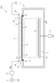
- FIG. 1 is a vertical cross-sectional view illustrating a configuration of a plasma processing apparatus according to an embodiment
- FIG. 2 is a cross-sectional view illustrating a schematic configuration of the plasma processing apparatus according to the embodiment.
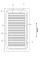
- FIG. 2 is a plan view showing a schematic configuration of a slit plate according to the embodiment, as viewed from the antenna side.
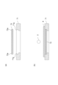
- 4A and 4B are longitudinal cross-sectional views showing a schematic configuration of the slit plate of the embodiment, in which FIG. 4A shows a state in which the beam-shaped member is removed, and FIG. 4B shows a state in which the beam-shaped member, the dielectric plate, and the antenna are installed.
- FIG. 4A shows a state in which the beam-shaped member is removed
- FIG. 4B shows a state in which the beam-shaped member, the dielectric plate, and the antenna are installed.
- FIG. 4A shows a state in which the beam-shaped member is removed
- FIG. 4B shows a state in which the beam-shaped member, the
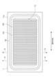
- FIG. 13 is a plan view showing a schematic configuration of a slit plate according to another embodiment, as viewed from the antenna side.
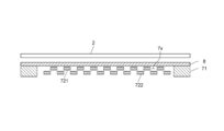
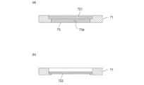
- 6A and 6B are longitudinal cross-sectional views showing the configuration of a slit plate of another embodiment, where (a) is a longitudinal cross-sectional view showing the A-A' line cross-section in FIG. 5, and (b) is a longitudinal cross-sectional view showing the B-B' line cross-section in FIG. 5.
- FIG. 11 is a cross-sectional view showing a schematic configuration of a slit plate according to another embodiment.
- FIG. 11 is a cross-sectional view showing a schematic configuration of a slit plate according to another embodiment.
- FIG. 10A and 10B are longitudinal sectional views each showing a schematic configuration of a slit plate according to another embodiment, in which FIG. 10A is a longitudinal sectional view showing a configuration in the vicinity of a first beam-like member, and FIG. 10B is a longitudinal sectional view showing a configuration in the vicinity of a second beam-like member.
- FIG. 11 is a cross-sectional view showing a schematic configuration of the slit plate and its vicinity in another embodiment.
- FIG. 11 is a vertical cross-sectional view showing a schematic configuration of the vicinity of a slit plate according to another embodiment.
- FIG. 11 is a vertical cross-sectional view showing a schematic configuration of the vicinity of a slit plate according to another embodiment.
- the plasma processing apparatus 100 of this embodiment processes a substrate O by using an inductively coupled plasma P.
- the substrate O is, for example, a substrate for a flat panel display (FPD) such as a liquid crystal display or an organic electroluminescence display, a flexible substrate for a flexible display, etc.
- the processing performed on the substrate O is, for example, film formation by a plasma CVD method, etching, ashing, sputtering, etc.
- the plasma processing apparatus 100 is also called a plasma CVD apparatus when film formation is performed by plasma CVD, a plasma etching apparatus when etching is performed, a plasma ashing apparatus when ashing is performed, and a plasma sputtering apparatus when sputtering is performed.
- the plasma processing apparatus 100 comprises a vacuum vessel 1 which forms a processing chamber which is evacuated and into which gas is introduced, an antenna 2 provided outside the vacuum vessel 1, and a high frequency power supply 3 which applies a high frequency to the antenna 2.
- a high frequency current IR flows through the antenna 2
- an induced electric field is generated within the vacuum vessel 1, and an inductively coupled plasma P is generated.
- the vacuum vessel 1 is, for example, a metal vessel, and an opening 1x is formed in its wall (here, the upper wall 1a) that penetrates in the thickness direction.
- the vacuum vessel 1 is electrically grounded here, and the processing chamber inside is evacuated by a vacuum exhaust device 4.
- Gas is introduced into the vacuum vessel 1 through, for example, a flow rate regulator (not shown) or one or more gas inlets 11 provided in the vacuum vessel 1.
- the gas may be selected according to the processing contents to be performed on the substrate O.
- the gas is a raw material gas or a gas obtained by diluting the raw material gas with a dilution gas (for example, H 2 ).
- a Si film can be formed on the substrate, when the raw material gas is SiH 4 +NH 3 , a SiN film can be formed, when the raw material gas is SiH 4 +O 2 , a SiO 2 film can be formed, and when the raw material gas is SiF 4 +N 2 , a SiN:F film (fluorinated silicon nitride film) can be formed.
- a bias voltage may be applied to the substrate holder 5 from a bias power supply 6.
- the bias voltage may be, for example, a negative DC voltage, a negative bias voltage, etc., but is not limited to these.
- a heater 51 for heating the substrate O may be provided inside the substrate holder 5.
- the antenna 2 is arranged to face the opening 1x formed in the vacuum vessel 1. Note that the number of antennas 2 is not limited to one, and multiple antennas 2 may be provided.
- one end of the antenna 2, the power supply end 2a, is connected to the high-frequency power source 3 via a matching circuit 31, and the other end, the termination end 2b, is directly grounded.
- the termination end 2b may also be grounded via a capacitor or a coil, etc.
- the high-frequency power supply 3 can pass a high-frequency current IR through the antenna 2 via a matching circuit 31.
- the frequency of the high-frequency current is, for example, a typical 13.56 MHz, but is not limited to this and may be changed as appropriate.
- This plasma processing apparatus 100 further includes a slit plate 7 that blocks the opening 1x formed in the wall (upper wall 1a) of the vacuum vessel 1 from outside the vacuum vessel 1, and a dielectric plate 8 that blocks the slit 7x formed in the slit plate 7 from outside the vacuum vessel 1.
- the slit plate 7 allows the high-frequency magnetic field generated by the antenna 2 to pass through the vacuum vessel 1, and prevents the electric field from entering the vacuum vessel 1 from the outside.
- the slit plate 7 is a flat rectangular plate with multiple slits 7x that penetrate in the thickness direction and are arranged at equal intervals along the longitudinal direction of the antenna 2.
- the slit plate 7 preferably has a higher mechanical strength than the dielectric plate 8 described below, and preferably has a larger thickness dimension than the dielectric plate 8.
- the multiple slits 7x are formed parallel to each other when viewed from the thickness direction and so as to intersect (specifically so as to intersect at right angles) with the antenna 2. All of the multiple slits 7x have the same shape (specifically, a rectangular shape when viewed from above), and the length (width) along the longitudinal direction of the antenna 2 is, for example, 5 mm to 30 mm, but is not limited to this.
- the slit plate 7 is larger than the opening 1x of the vacuum vessel 1 in a plan view, and is supported by the upper wall 1a to close the opening 1x.
- a sealing member S1 (see Figures 1 and 2), such as an O-ring or a gasket, is interposed between the slit plate 7 and the upper wall 1a, creating a vacuum seal between them.
- the dielectric plate 8 is provided on the outward surface 7a of the slit plate 7 that faces the outside of the vacuum vessel 1 (the back side of the inward surface 7b that faces the inside of the vacuum vessel 1) and covers the slits 7x of the slit plate 7.
- the dielectric plate 8 is a flat plate made entirely of a dielectric material, and is made of, for example, ceramics such as alumina, silicon carbide, silicon nitride, etc., inorganic materials such as quartz glass and non-alkali glass, and resin materials such as fluororesin (e.g. Teflon). From the viewpoint of reducing dielectric loss, the material making up the dielectric plate 8 preferably has a dielectric tangent of 0.01 or less, and more preferably 0.005 or less.
- the thickness of the dielectric plate 8 is made smaller than that of the slit plate 7, but this is not limiting, and it is sufficient that the plate has the strength to withstand the pressure difference between the inside and outside of the vacuum vessel 1 received through the slits 7x when the vacuum vessel 1 is evacuated, and may be set appropriately according to the specifications such as the number and length of the slits 7x. However, from the viewpoint of shortening the distance between the antenna 2 and the vacuum vessel 1, a thinner plate is preferable.
- a sealing member S2 such as an O-ring or gasket is interposed between the dielectric plate 8 and the slit plate 7, and a vacuum seal is formed between them.
- the slit plate 7 and the dielectric plate 8 function as a magnetic field transmission window W that allows the magnetic field generated from the antenna 2 to pass through.
- the high frequency magnetic field generated from the antenna 2 passes through the magnetic field transmission window W consisting of the slit plate 7 and the dielectric plate 8 and is formed (supplied) inside the vacuum vessel 1.
- an induced electric field is generated in the space inside the vacuum vessel 1, and an inductively coupled plasma P is generated.
- the slit plate 7 comprises an annular frame 71 and a number of beam members 72 aligned and spanned across the frame 71, with the slits 7X being formed by the gaps between the beam members 72.
- the frame 71 and the beam members 72 that constitute the slit plate 7 are both electrically connected to the vacuum vessel 1 and are at ground potential.
- the frame 71 is a plate-shaped metal material such as one metal selected from the group including Cu, Al, Zn, Ni, Sn, Si, Ti, Fe, Cr, Nb, C, Mo, W, or Co, or an alloy thereof (e.g., stainless steel alloy, aluminum alloy, etc.).
- the frame 71 is shaped to border a rectangular opening 71a in a plan view from the antenna 2 side, and both the outer peripheral edge 71o and the inner peripheral edge 71i are rectangular.
- the inner peripheral edge 71i of the frame 71 has a plurality of grooves 71g formed in pairs on either side of the opening 71a.
- the plurality of pairs of grooves 71g are formed by cutting out a pair of opposing parallel sides along the longitudinal direction of the antenna 2, and are formed at equal intervals along the longitudinal direction of the antenna 2.
- the plurality of grooves 71g all have the same cross-sectional shape (here, rectangular) and are all formed to have approximately the same depth.
- the beam member 72 is elongated and extends in a direction perpendicular to the antenna 2, and in this embodiment, has a substantially uniform cross-sectional shape along the longitudinal direction. Both ends 72a of the beam member 72 along the longitudinal direction have a substantially uniform cross-sectional shape as the groove 71g of the frame body 71, and the multiple beam members 72 are bridged across the frame body 71 at the same height by fitting the both ends 72a into the groove 71g of the frame body 71.
- the multiple beam members 72 are all of the same shape with the same length and width, and are detachably attached to the frame body 71 at substantially equal intervals along the longitudinal direction of the antenna 2. As shown in FIG. 4, the height dimension of the beam member 72 is substantially the same as or smaller than the depth dimension of the groove 71g of the frame body 71.
- the beam member 72 is made of a metal material such as one metal selected from the group including Cu, Al, Zn, Ni, Sn, Si, Ti, Fe, Cr, Nb, C, Mo, W, or Co, or an alloy thereof (e.g., stainless steel alloy, aluminum alloy, etc.).
- a metal material such as one metal selected from the group including Cu, Al, Zn, Ni, Sn, Si, Ti, Fe, Cr, Nb, C, Mo, W, or Co, or an alloy thereof (e.g., stainless steel alloy, aluminum alloy, etc.).
- it is made of a material such as SUS that has a higher Young's modulus than the frame body 71.
- the slit plate 7 is composed of a frame 71 and a plurality of beam members 72 that are spanned across the frame 71, and the gaps between the beam members 72 form the slits 7x. Therefore, when cleaning, the beam members 72 that are dirty due to deposits or the like can be removed from the frame 71 and replaced, eliminating the need to clean the plurality of slits 7x one by one, and making maintenance easier. Furthermore, by configuring the slit plate 7 as two types of members, the frame 71 and the beam members 72, the processing of each member can be simplified compared to when the slit plate 7 is formed by processing one metal plate.
- the slit plate 7 can be made thinner. This makes it possible to further shorten the distance from the antenna 2 to the vacuum vessel 1, and to more efficiently supply the high-frequency magnetic field generated by the antenna 2 into the vacuum vessel 1.
- the multiple beam members 72 are all attached to the frame body 71 so that they are the same height, but this is not limited to this.
- the slit plate 7 has multiple first beam members 721 and second beam members 722 that are spanned across the frame body 71 at different heights, as shown in Figures 5, 6, and 7, and the first beam members 721 and second beam members 722 may be arranged alternately along the longitudinal direction of the antenna 2.
- first grooves 711g and second grooves 712g having different depths are formed alternately in the frame body 71 along the longitudinal direction of the antenna 2, and the first beam members 721 and second beam members 722 may be spanned across the first grooves 711g and second grooves 712g, respectively.
- the first beam member 721 is configured to be located closer to the antenna 2 than the second beam member 722 (i.e., the second groove 712g is deeper than the first groove 711g).
- the first beam member 721 and the second beam member 722 are attached to the frame 71 so that they do not come into contact with each other.
- the top surface (the surface facing the antenna 2) of the second beam member 722 fitted into the second groove 712g is configured to be lower than the position of the bottom surface of the first groove 711g
- the bottom surface (the surface facing the processing chamber) of the first beam member 721 is configured to be higher than the top surface of the second beam member 722.
- the first beam member 721 and the second beam member 722 are arranged without gaps and without overlapping each other in a plan view from the antenna 2 side.
- the gap dimension between the first beam member 721 and the width dimension of the second beam member 722 are equal, and the gap dimension between the second beam member 722 and the width dimension of the first beam member 721 are equal.
- the slit plate 7 may have a shielding wall 73 for shielding charged particles moving along the longitudinal direction of the antenna 2 between the first beam member 721 and the second beam member 722.
- This shielding wall 73 may have a wall surface 73a formed so as to intersect (specifically, perpendicular to) the longitudinal direction of the antenna 2.
- This wall surface 73a is elongated and extends in a direction intersecting the antenna 2, and is preferably approximately the same length as the length of the opening 71a of the frame 71.
- this shielding wall 73 may be formed by a protrusion protruding from one of the first beam member 721 and the second beam member 722 toward the gap between the other beam member.
- the slit plate 7 may have a plurality of shielding walls 73 along the longitudinal direction of the antenna 2.
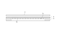
- the cross-sectional shape of the groove 71g is rectangular, but this is not limited to this. In other embodiments, as shown in FIG. 10, the cross-sectional shape of the groove 71g may be V-shaped or partially circular. Also, the cross-sectional shape of the beam member 72 may be triangular or circular to match the cross-sectional shape of the groove 71g.
- the beam member 72 may have a film-adhesion suppression protrusion 74 that protrudes toward the processing chamber in an area other than both ends 72a that are hung in the groove 71g.
- This film-adhesion suppression protrusion 74 is intended to prevent deposits from adhering to the groove 71g in which the beam member 72 is hung, and faces the inner peripheral surface 71s of the frame body 71 when viewed from the longitudinal direction of the antenna 2, and has a covering surface 74a that covers the inner peripheral surface 71s.
- the film-adhesion suppression protrusion may be provided only near both ends 72a of the beam member 72 as shown in FIG. 11, or may be formed over the entire opening 71a as shown in FIG. 12.
- the disclosure of this specification may further include the following aspects 1-7.
- a plasma processing apparatus that generates plasma within a processing chamber by passing a high-frequency current through an antenna provided outside a vacuum vessel that forms the processing chamber, the plasma processing apparatus comprising: a slit plate provided to cover an opening formed in a position facing the antenna of the vacuum vessel; and a dielectric plate that covers the slits formed in the slit plate from the outside of the vacuum vessel, the slit plate comprising a ring-shaped frame body and a plurality of beam-shaped members aligned and spanned across the frame body, and the slits are formed by the gaps between the plurality of beam-shaped members.
- the slit plate is composed of a frame body and a plurality of beam-like members spanned over the frame body, and the slits are formed by the gaps between the beam-like members. Therefore, when cleaning, it is sufficient to remove the beam-like members that are dirty due to deposits from the frame body and replace them, so that the labor of cleaning the plurality of slits one by one can be eliminated, and maintenance can be easily performed. Furthermore, by configuring the slit plate as two types of members, the frame body and the beam-like members, it is possible to simplify the processing of each member compared to the case where a slit plate is formed by processing a single metal plate.
- the beam member can be attached to the frame by hanging it in the groove, so that displacement of the beam member can be prevented and the beam member can be easily attached and removed.
- a plasma processing apparatus according to aspect 2 or 3, wherein the beam member has a protrusion protruding toward the processing chamber in an area other than both ends that are bridged over the groove.
- the protrusion protruding toward the processing chamber functions as a cover that prevents deposits from adhering to the inner peripheral surface of the frame, thereby reducing the amount of deposits that adhere to the frame and further improving maintainability.
- the first beam members and the second beam members are alternately arranged along the longitudinal direction of the antenna in a plan view, so that the dielectric plate is hidden when viewed from inside the vacuum vessel, and therefore it is possible to prevent conductive flying objects and the like from adhering to and contaminating the dielectric plate.
- the second beam-shaped member is positioned between the first beam-shaped members, the dielectric plate exposed from the slits between the first beam-shaped members is not directly exposed to the plasma or the workpiece, thereby suppressing the temperature rise of the dielectric plate due to radiation, etc., and preventing damage. Furthermore, since the first beam member and the second beam member are different in height, the induced current generated in the slit plate along the antenna can be reduced, and the decrease in the transmittance of the high-frequency magnetic field can be efficiently suppressed.
- the present invention improves the maintainability of the slit plate in a plasma processing apparatus in which an antenna is placed outside a vacuum vessel and a magnetic field transmission window is formed by overlapping a dielectric plate and a slit plate.
- Plasma processing apparatus P Inductively coupled plasma 1: Vacuum vessel 2: Antenna 3: High frequency power supply 7: Slit plate 71: Frame 71i: Inner periphery 72: Beam-shaped member 7x: Slit 8: Dielectric plate
Landscapes
- Chemical & Material Sciences (AREA)
- Engineering & Computer Science (AREA)
- Physics & Mathematics (AREA)
- Plasma & Fusion (AREA)
- Analytical Chemistry (AREA)
- Organic Chemistry (AREA)
- Mechanical Engineering (AREA)
- Metallurgy (AREA)
- Materials Engineering (AREA)
- Chemical Kinetics & Catalysis (AREA)
- General Chemical & Material Sciences (AREA)
- Power Engineering (AREA)
- Electromagnetism (AREA)
- Spectroscopy & Molecular Physics (AREA)
- Plasma Technology (AREA)
- Drying Of Semiconductors (AREA)
- Chemical Vapour Deposition (AREA)
Abstract
Description
本実施形態のプラズマ処理装置100は、誘導結合型のプラズマPを用いて基板Oに処理を施すものである。ここで、基板Oは、例えば、液晶ディスプレイや有機ELディスプレイ等のフラットパネルディスプレイ(FPD)用の基板、フレキシブルディスプレイ用のフレキシブル基板等である。また、基板Oに施す処理は、例えば、プラズマCVD法による膜形成、エッチング、アッシング、スパッタリング等である。
このように構成した本実施形態のプラズマ処理装置100によれば、スリット板7が、枠体71と、枠体71に架け渡された複数の梁状部材72とにより構成され、梁状部材72間の隙間によりスリット7xを形成するようにしているので、清掃時には、堆積物の付着等のより汚れた梁状部材72を枠体71から取り外して交換すればよいので、複数のスリット7xを1つ1つ清掃する手間が省くことができ、メンテナンスを簡単に行うことができるようになる。さらに、スリット板7を、枠体71と梁状部材72の2種類の部材に分けて構成することで、1枚の金属板を加工してスリット板7を形成する場合に比べて、個々の部材の加工を簡単にすることができる。そのため、切削が容易なアルミニウムのような材料を用いる必要がなく、より強度が高いSUS等の金属材料を用いることができ、スリット板7の薄型化を図ることができる。これにより、アンテナ2から真空容器1までの距離を一層短くでき、アンテナ2から生じた高周波磁場をより効率良く真空容器1内に供給することができる。
なお、本発明は前記実施形態に限られるものではない。
このような構成であれば、スリット板が、枠体と、枠体に架け渡された複数の梁状部材とにより構成され、梁状部材間の隙間によりスリットを形成するようにしているので、清掃時には、堆積物の付着等のより汚れた梁状部材を枠体から取り外して交換すればよいので、複数のスリットを1つ1つ清掃する手間が省くことができ、メンテナンスを簡単に行うことができるようになる。さらに、スリット板を、枠体と梁状部材の2種類の部材に分けて構成することで、1枚の金属板を加工してスリット板を形成する場合に比べて、個々の部材の加工を簡単にすることができる。そのため、切削が容易なアルミニウムのような材料を用いる必要がなく、より強度が高いSUS等の金属材料を用いることができ、スリット板の薄型化を図ることができる。これにより、アンテナから真空容器までの距離を短くすることができ、アンテナから生じた高周波磁場を効率良く真空容器内に供給することができる。
このような構成であれば、溝に梁状部材をかけることにより梁状部材を枠体に取り付けられるので、梁状部材の位置ずれを防止することができ、また梁状部材の取り付け及び取り外しが容易である。
溝の断面が矩形状である場合にはザグリに起因して溝内で梁状部材の位置ずれが生じる可能性があるが、溝の断面形状をV字形状や部分円形状とすることで、このような位置ズレの問題を解消することができる。
このような構成であれば、処理室側に突出する突起部が、枠体の内側周面への堆積物の付着を抑制するカバーとして機能し、枠体に付着する堆積物を低減することができ、メンテナンス性をより向上することができる。
このような構成であれば、平面視において、アンテナの長手方向に沿って第1の梁状部材と第2の梁状部材とが交互に並ぶようにすることで、真空容器の内側から視て誘電体板が隠れるようにしているので、導電性の飛来物等が誘電体板に付着して汚染するのを防止できる。これにより、誘電体板の表面が導電化されるのを防ぎ、高周波磁場の透過率の低下を抑制できるとともに、誘電体板の表面に誘導電流が流れることによる発熱も防止することができる。
また、第1の梁状部材間に第2の梁状部材が位置するようにしているので、第1の梁状部材間のスリットから露出する誘電体板がプラズマや被処理物に直接晒されないので、輻射等による誘電体板の温度上昇を抑えて破損を防止できる。
しかも、第1の梁状部材と第2の梁状部材とを高さ違いにしているので、アンテナに沿ってスリット板に生じる誘導電流を小さくでき、高周波磁場の透過率の低下を効率よく抑制できる。
このようにすれば、真空容器の内側から視て誘電体板がしっかり隠れるようになるので、導電性の飛来物等が誘電体板に付着して汚染するのをより防止できる。
このようにすれば、第1の梁状部材と第2の梁状部材との間の間隙内におけるアンテナの長手方向に沿った荷電粒子の運動を遮蔽壁により抑制でき、間隙内での放電発生を防止できる。
P ・・・誘導結合プラズマ
1 ・・・真空容器
2 ・・・アンテナ
3 ・・・高周波電源
7 ・・・スリット板
71 ・・・枠体
71i・・・内周縁
72 ・・・梁状部材
7x ・・・スリット
8 ・・・誘電体板
Claims (7)
- 処理室を形成する真空容器の外部に設けられたアンテナに高周波電流を流して前記処理室内にプラズマを発生させるプラズマ処理装置であって、
前記真空容器の前記アンテナに臨む位置に形成された開口を塞ぐように設けられたスリット板と、
前記スリット板に形成されたスリットを前記真空容器の外側から塞ぐ誘電体板とを備え、
前記スリット板が、環状の枠体と、当該枠体に並べて架け渡された複数の梁状部材とを具備し、当該複数の梁状部材間の隙間により前記スリットを形成するものであるプラズマ処理装置。 - 前記枠体の内周縁部にはその開口を挟んで対をなす複数の溝が形成されており、
当該対をなす各溝に前記梁状部材の両端部が掛けられている請求項1に記載のプラズマ処理装置。 - 前記溝の断面形状がV字形状又は部分円形状である請求項2に記載のプラズマ処理装置。
- 前記梁状部材が、前記溝に架けられる両端部以外の領域に、前記処理室側に向かって突出する突起部を有している請求項2に記載のプラズマ処理装置。
- 前記スリット板が、板厚方向において高さ違いで前記枠体に架け渡された第1の前記梁状部材と第2の前記梁状部材とを具備し、
前記第1の梁状部材と前記第2の梁状部材とが前記アンテナの長手方向に沿って交互に並んで配置されている請求項1に記載のプラズマ処理装置。 - 前記アンテナの長手方向において、前記第1の梁状部材間の隙間寸法と前記第2の梁状部材の幅寸法とが略同一である請求項5に記載のプラズマ処理装置。
- 前記スリット板が、前記第1の梁状部材と前記第2の梁状部材との間において、前記アンテナの長手方向に沿って運動する荷電粒子を遮蔽するための遮蔽壁を有する請求項6に記載のプラズマ処理装置。
Priority Applications (2)
| Application Number | Priority Date | Filing Date | Title |
|---|---|---|---|
| CN202380071391.3A CN119999337A (zh) | 2022-11-07 | 2023-09-27 | 等离子体处理装置 |
| KR1020257009682A KR20250056967A (ko) | 2022-11-07 | 2023-09-27 | 플라스마 처리 장치 |
Applications Claiming Priority (2)
| Application Number | Priority Date | Filing Date | Title |
|---|---|---|---|
| JP2022-177963 | 2022-11-07 | ||
| JP2022177963A JP7891641B2 (ja) | 2022-11-07 | 2022-11-07 | プラズマ処理装置 |
Publications (1)
| Publication Number | Publication Date |
|---|---|
| WO2024101024A1 true WO2024101024A1 (ja) | 2024-05-16 |
Family
ID=91032273
Family Applications (1)
| Application Number | Title | Priority Date | Filing Date |
|---|---|---|---|
| PCT/JP2023/035207 Ceased WO2024101024A1 (ja) | 2022-11-07 | 2023-09-27 | プラズマ処理装置 |
Country Status (5)
| Country | Link |
|---|---|
| JP (1) | JP7891641B2 (ja) |
| KR (1) | KR20250056967A (ja) |
| CN (1) | CN119999337A (ja) |
| TW (1) | TWI893477B (ja) |
| WO (1) | WO2024101024A1 (ja) |
Cited By (1)
| Publication number | Priority date | Publication date | Assignee | Title |
|---|---|---|---|---|
| CN121709505A (zh) * | 2026-02-13 | 2026-03-20 | 上海邦芯半导体科技有限公司 | 一种反应腔室及晶圆处理设备 |
Citations (8)
| Publication number | Priority date | Publication date | Assignee | Title |
|---|---|---|---|---|
| JP2001254188A (ja) * | 2000-03-10 | 2001-09-18 | Samco International Inc | 誘導結合形プラズマ処理装置 |
| JP2014026773A (ja) * | 2012-07-25 | 2014-02-06 | Tokyo Electron Ltd | プラズマ処理装置 |
| US20140097752A1 (en) * | 2012-10-09 | 2014-04-10 | Varian Semiconductor Equipment Associates, Inc. | Inductively Coupled Plasma ION Source Chamber with Dopant Material Shield |
| US20140342568A1 (en) * | 2013-05-16 | 2014-11-20 | Lam Research Corporation | Controlling temperature of a faraday shield |
| WO2020188809A1 (ja) * | 2019-03-20 | 2020-09-24 | 日新電機株式会社 | プラズマ処理装置 |
| JP2020198282A (ja) * | 2019-06-05 | 2020-12-10 | 日新電機株式会社 | プラズマ処理装置 |
| WO2021210583A1 (ja) * | 2020-04-13 | 2021-10-21 | 日新電機株式会社 | プラズマ源及びプラズマ処理装置 |
| WO2023136008A1 (ja) * | 2022-01-17 | 2023-07-20 | 日新電機株式会社 | プラズマ処理装置 |
Family Cites Families (4)
| Publication number | Priority date | Publication date | Assignee | Title |
|---|---|---|---|---|
| US6946054B2 (en) * | 2002-02-22 | 2005-09-20 | Tokyo Electron Limited | Modified transfer function deposition baffles and high density plasma ignition therewith in semiconductor processing |
| JP3714924B2 (ja) * | 2002-07-11 | 2005-11-09 | 東京エレクトロン株式会社 | プラズマ処理装置 |
| WO2020246523A1 (ja) * | 2019-06-05 | 2020-12-10 | 日新電機株式会社 | プラズマ処理装置 |
| JP7568915B2 (ja) * | 2020-11-27 | 2024-10-17 | 日新電機株式会社 | プラズマ処理装置 |
-
2022
- 2022-11-07 JP JP2022177963A patent/JP7891641B2/ja active Active
-
2023
- 2023-09-27 WO PCT/JP2023/035207 patent/WO2024101024A1/ja not_active Ceased
- 2023-09-27 KR KR1020257009682A patent/KR20250056967A/ko active Pending
- 2023-09-27 CN CN202380071391.3A patent/CN119999337A/zh active Pending
- 2023-10-11 TW TW112138782A patent/TWI893477B/zh active
Patent Citations (8)
| Publication number | Priority date | Publication date | Assignee | Title |
|---|---|---|---|---|
| JP2001254188A (ja) * | 2000-03-10 | 2001-09-18 | Samco International Inc | 誘導結合形プラズマ処理装置 |
| JP2014026773A (ja) * | 2012-07-25 | 2014-02-06 | Tokyo Electron Ltd | プラズマ処理装置 |
| US20140097752A1 (en) * | 2012-10-09 | 2014-04-10 | Varian Semiconductor Equipment Associates, Inc. | Inductively Coupled Plasma ION Source Chamber with Dopant Material Shield |
| US20140342568A1 (en) * | 2013-05-16 | 2014-11-20 | Lam Research Corporation | Controlling temperature of a faraday shield |
| WO2020188809A1 (ja) * | 2019-03-20 | 2020-09-24 | 日新電機株式会社 | プラズマ処理装置 |
| JP2020198282A (ja) * | 2019-06-05 | 2020-12-10 | 日新電機株式会社 | プラズマ処理装置 |
| WO2021210583A1 (ja) * | 2020-04-13 | 2021-10-21 | 日新電機株式会社 | プラズマ源及びプラズマ処理装置 |
| WO2023136008A1 (ja) * | 2022-01-17 | 2023-07-20 | 日新電機株式会社 | プラズマ処理装置 |
Cited By (1)
| Publication number | Priority date | Publication date | Assignee | Title |
|---|---|---|---|---|
| CN121709505A (zh) * | 2026-02-13 | 2026-03-20 | 上海邦芯半导体科技有限公司 | 一种反应腔室及晶圆处理设备 |
Also Published As
| Publication number | Publication date |
|---|---|
| JP7891641B2 (ja) | 2026-07-17 |
| TWI893477B (zh) | 2025-08-11 |
| TW202420895A (zh) | 2024-05-16 |
| KR20250056967A (ko) | 2025-04-28 |
| CN119999337A (zh) | 2025-05-13 |
| JP2024067696A (ja) | 2024-05-17 |
Similar Documents
| Publication | Publication Date | Title |
|---|---|---|
| TWI839420B (zh) | 電漿沉積腔室及用以在基板上沉積多層膜之方法 | |
| JP4217299B2 (ja) | 処理装置 | |
| CN101647090B (zh) | 射频遮板及沉积方法 | |
| TWI588290B (zh) | 處理設備與清潔方法 | |
| JP7232410B2 (ja) | プラズマ処理装置 | |
| TWI756670B (zh) | 電漿處理裝置 | |
| CN108807124B (zh) | 基板处理装置 | |
| JP7238613B2 (ja) | プラズマ処理装置 | |
| KR20170092135A (ko) | 플라즈마 처리 용기 및 플라즈마 처리 장치 | |
| KR20240107361A (ko) | 고밀도 플라즈마 강화 프로세스 챔버 | |
| CN110546733A (zh) | 在处理腔室中防止工件上的材料沉积 | |
| JP7469625B2 (ja) | プラズマ源及びプラズマ処理装置 | |
| JP2024067696A (ja) | プラズマ処理装置 | |
| TWI847456B (zh) | 電漿處理裝置 | |
| JP7440746B2 (ja) | プラズマ源及びプラズマ処理装置 | |
| JP7403052B2 (ja) | プラズマ源及びプラズマ処理装置 | |
| KR101246859B1 (ko) | 플라즈마 처리장치 | |
| JP7610122B2 (ja) | プラズマ源及びプラズマ処理装置 | |
| JP7688258B2 (ja) | プラズマ処理装置 | |
| TWI905616B (zh) | 電漿處理裝置 | |
| JP2023067033A (ja) | 基板処理装置及び基板処理方法 | |
| US20090261066A1 (en) | Apparatus and method for dry etching |
Legal Events
| Date | Code | Title | Description |
|---|---|---|---|
| 121 | Ep: the epo has been informed by wipo that ep was designated in this application |
Ref document number: 23888377 Country of ref document: EP Kind code of ref document: A1 |
|
| ENP | Entry into the national phase |
Ref document number: 20257009682 Country of ref document: KR Kind code of ref document: A |
|
| WWE | Wipo information: entry into national phase |
Ref document number: 1020257009682 Country of ref document: KR |
|
| WWE | Wipo information: entry into national phase |
Ref document number: 202380071391.3 Country of ref document: CN |
|
| WWP | Wipo information: published in national office |
Ref document number: 1020257009682 Country of ref document: KR |
|
| WWP | Wipo information: published in national office |
Ref document number: 202380071391.3 Country of ref document: CN |
|
| NENP | Non-entry into the national phase |
Ref country code: DE |
|
| 122 | Ep: pct application non-entry in european phase |
Ref document number: 23888377 Country of ref document: EP Kind code of ref document: A1 |