WO2024100949A1 - インダクタ部品 - Google Patents
インダクタ部品 Download PDFInfo
- Publication number
- WO2024100949A1 WO2024100949A1 PCT/JP2023/029300 JP2023029300W WO2024100949A1 WO 2024100949 A1 WO2024100949 A1 WO 2024100949A1 JP 2023029300 W JP2023029300 W JP 2023029300W WO 2024100949 A1 WO2024100949 A1 WO 2024100949A1
- Authority
- WO
- WIPO (PCT)
- Prior art keywords
- inductor
- wiring
- inductor wiring
- magnetic layer
- insulating layer
- Prior art date
- Legal status (The legal status is an assumption and is not a legal conclusion. Google has not performed a legal analysis and makes no representation as to the accuracy of the status listed.)
- Ceased
Links
Images


Classifications
-
- H—ELECTRICITY
- H01—ELECTRIC ELEMENTS
- H01F—MAGNETS; INDUCTANCES; TRANSFORMERS; SELECTION OF MATERIALS FOR THEIR MAGNETIC PROPERTIES
- H01F27/00—Details of transformers or inductances, in general
- H01F27/28—Coils; Windings; Conductive connections
- H01F27/32—Insulating of coils, windings, or parts thereof
- H01F27/324—Insulation between coil and core, between different winding sections, around the coil; Other insulation structures
-
- H—ELECTRICITY
- H01—ELECTRIC ELEMENTS
- H01F—MAGNETS; INDUCTANCES; TRANSFORMERS; SELECTION OF MATERIALS FOR THEIR MAGNETIC PROPERTIES
- H01F17/00—Fixed inductances of the signal type
-
- H—ELECTRICITY
- H01—ELECTRIC ELEMENTS
- H01F—MAGNETS; INDUCTANCES; TRANSFORMERS; SELECTION OF MATERIALS FOR THEIR MAGNETIC PROPERTIES
- H01F17/00—Fixed inductances of the signal type
- H01F17/0006—Printed inductances
-
- H—ELECTRICITY
- H01—ELECTRIC ELEMENTS
- H01F—MAGNETS; INDUCTANCES; TRANSFORMERS; SELECTION OF MATERIALS FOR THEIR MAGNETIC PROPERTIES
- H01F17/00—Fixed inductances of the signal type
- H01F17/04—Fixed inductances of the signal type with magnetic core
-
- H—ELECTRICITY
- H01—ELECTRIC ELEMENTS
- H01F—MAGNETS; INDUCTANCES; TRANSFORMERS; SELECTION OF MATERIALS FOR THEIR MAGNETIC PROPERTIES
- H01F27/00—Details of transformers or inductances, in general
- H01F27/28—Coils; Windings; Conductive connections
- H01F27/29—Terminals; Tapping arrangements for signal inductances
- H01F27/292—Surface mounted devices
-
- H—ELECTRICITY
- H01—ELECTRIC ELEMENTS
- H01F—MAGNETS; INDUCTANCES; TRANSFORMERS; SELECTION OF MATERIALS FOR THEIR MAGNETIC PROPERTIES
- H01F27/00—Details of transformers or inductances, in general
- H01F27/28—Coils; Windings; Conductive connections
- H01F27/32—Insulating of coils, windings, or parts thereof
-
- H—ELECTRICITY
- H01—ELECTRIC ELEMENTS
- H01F—MAGNETS; INDUCTANCES; TRANSFORMERS; SELECTION OF MATERIALS FOR THEIR MAGNETIC PROPERTIES
- H01F17/00—Fixed inductances of the signal type
- H01F17/0006—Printed inductances
- H01F2017/004—Printed inductances with the coil helically wound around an axis without a core
-
- H—ELECTRICITY
- H01—ELECTRIC ELEMENTS
- H01F—MAGNETS; INDUCTANCES; TRANSFORMERS; SELECTION OF MATERIALS FOR THEIR MAGNETIC PROPERTIES
- H01F17/00—Fixed inductances of the signal type
- H01F17/04—Fixed inductances of the signal type with magnetic core
- H01F2017/048—Fixed inductances of the signal type with magnetic core with encapsulating core, e.g. made of resin and magnetic powder
Definitions
- This disclosure relates to inductor components.
- the inductor component comprises an element body including a magnetic layer, and a coil disposed within the element body and having an axis. The entire outer surface of the coil is covered with an insulating material.
- the entire outer surface of the coil is covered with an insulating material, which means that the volume of the magnetic layer cannot be secured, and the desired inductance value cannot always be obtained.
- the objective of this disclosure is to provide an inductor component that can improve the inductance value.
- an inductor component comprises: An element including a magnetic layer; a coil disposed within the element body and having an axis; an insulating layer covering a portion of an outer surface of the coil; The coil has an inductor wiring wound along a plane perpendicular to the axis, the inductor wiring has a first surface and a second surface opposed to each other in the axial direction; At least a portion of the first surface of the inductor wiring is in contact with the magnetic layer.
- the inductance value of the inductor component can be improved.
- the inductor component according to one aspect of the present disclosure can improve the inductance value.
- FIG. 1 is a schematic plan view showing a first embodiment of an inductor component; This is a cross-sectional view of FIG. 1 taken along line II-II.
- FIG. 3 is an enlarged view of part A in FIG. 2 .
- 11 is a schematic cross-sectional view showing a modified example of the inductor component.
- FIG. 1A to 1C are explanatory diagrams illustrating a method for manufacturing an inductor component.
- 1A to 1C are explanatory diagrams illustrating a method for manufacturing an inductor component.
- 1A to 1C are explanatory diagrams illustrating a method for manufacturing an inductor component.
- 1A to 1C are explanatory diagrams illustrating a method for manufacturing an inductor component.
- 1A to 1C are explanatory diagrams illustrating a method for manufacturing an inductor component.
- 1A to 1C are explanatory diagrams illustrating a method for manufacturing an inductor component.
- 1A to 1C are explanatory diagrams illustrating a method for manufacturing an inductor component.
- 1A to 1C are explanatory diagrams illustrating a method for manufacturing an inductor component.
- 1A to 1C are explanatory diagrams illustrating a method for manufacturing an inductor component.
- FIG. 4 is a schematic cross-sectional view showing a second embodiment of the inductor component.
- FIG. 11 is a schematic cross-sectional view showing a third embodiment of the inductor component.
- FIG. 13 is a schematic plan view showing a fourth embodiment of an inductor component.
- FIG. 1 is a schematic plan view showing a first embodiment of an inductor component.
- Fig. 2 is a cross-sectional view taken along line II-II of Fig. 1.
- Fig. 1 has oblique lines drawn at positions where the top surface of the covering insulating layer is present.
- Fig. 2 omits the seed layer.
- Fig. 2 corresponds to an example of a "cross section perpendicular to the extending direction of the inductor wiring" as set forth in the claims.
- the inductor component 1 is mounted in, for example, electronic devices such as personal computers, DVD players, digital cameras, TVs, mobile phones, and car electronics, and is, for example, a component having an overall rectangular parallelepiped shape.
- the shape of the inductor component 1 is not particularly limited, and may be a cylindrical shape, a polygonal columnar shape, a truncated cone shape, or a polygonal truncated cone shape.
- the inductor component 1 comprises an element body 10, a coil 15 disposed within the element body 10 and having an axis AX, a coating insulating layer 30 and an underlying insulating layer 70 covering a portion of the outer surface of the coil 15, a first external terminal 51 and a second external terminal 52 exposed on the first main surface 10a of the element body 10, and a coating film 60 provided on the first main surface 10a of the element body 10.
- the coating insulating layer 30 and the underlying insulating layer 70 correspond to an example of an "insulating layer" as defined in the claims.
- the shape of the element body 10 is not particularly limited, but in this embodiment it is a rectangular parallelepiped.
- the outer surface of the element body 10 has a first main surface 10a and a second main surface 10b, and a first side surface 10c, a second side surface 10d, a third side surface 10e, and a fourth side surface 10f that are located between the first main surface 10a and the second main surface 10b and connect the first main surface 10a and the second main surface 10b.
- the first main surface 10a and the second main surface 10b face each other.
- the first side surface 10c and the second side surface 10d face each other.
- the third side surface 10e and the fourth side surface 10f face each other.
- the thickness direction of the element body 10 is the Z direction
- the direction from the second main surface 10b to the first main surface 10a is the forward Z direction
- the reverse direction of the forward Z direction is the reverse Z direction.
- the main surface side of the first main surface 10a and the second main surface 10b on which the external terminals 51 and 52 are provided is the upper side.
- the forward Z direction is the upper side.
- the length direction of the element body 10 in which the first external terminal 51 and the second external terminal 52 are arranged is the X direction
- the width direction of the element body 10 perpendicular to the length direction is the Y direction.
- the X direction from the first side surface 10c to the second side surface 10d is the forward X direction
- the reverse direction of the forward X direction is the reverse X direction
- the direction from the third side surface 10e to the fourth side surface 10f is the forward Y direction
- the reverse direction of the forward Y direction is the reverse Y direction.
- the forward Z direction corresponds to an example of the "first direction” described in the claims.
- the reverse Z direction corresponds to an example of the "second direction" described in the claims.
- the base body 10 includes a first magnetic layer 11 and a second magnetic layer 12 arranged in sequence along the forward Z direction. This "sequentially” refers simply to the positional relationship between the first magnetic layer 11 and the second magnetic layer 12, and has nothing to do with the order in which the first magnetic layer 11 and the second magnetic layer 12 are formed.
- the first magnetic layer 11 and the second magnetic layer 12 correspond to an example of a "magnetic layer" as described in the claims.
- the first magnetic layer 11 and the second magnetic layer 12 each contain a magnetic powder and a resin containing the magnetic powder.
- the resin is, for example, an organic insulating material such as epoxy, a mixture of epoxy and acrylic, or a mixture of epoxy, acrylic, and other materials.
- the magnetic powder is, for example, an FeSi-based alloy such as FeSiCr, an FeCo-based alloy, an Fe-based alloy such as NiFe, or an amorphous alloy thereof.
- the magnetic powder may be ferrite.
- the average particle size of the magnetic powder is preferably 5 ⁇ m or less.
- the first magnetic layer 11 and the second magnetic layer 12 may not contain an organic resin, such as a sintered body of ferrite or magnetic powder.
- the coil 15 has an inductor wiring 150 and a first lead-out wiring 21 and a second lead-out wiring 22 provided in the element body 10 so that their end faces are exposed from the first main surface 10a of the element body 10.
- the inductor wiring refers to a wiring wound in a spiral shape on a plane including the inner peripheral end 151 and the outer peripheral end 152.
- the coil is a member including not only the inductor wiring but also wiring (in this embodiment, the first and second lead-out wirings 21 and 22) that extracts the signal of the inductor wiring to the outside of the element body 10.
- the inductor wiring 150 is wound between the first magnetic layer 11 and the second magnetic layer 12 along a plane (XY plane) perpendicular to the axis AX of the coil 15. Specifically, the first magnetic layer 11 is located in the reverse Z direction from the inductor wiring 150, and the second magnetic layer 12 is located in the forward Z direction from the inductor wiring 150 and in a direction perpendicular to the forward Z direction.
- the inductor wiring 150 When viewed from the Z direction, the inductor wiring 150 is wound in a spiral shape in the clockwise direction from the outer peripheral end 152 to the inner peripheral end 151.
- the number of turns of the inductor wiring 150 is preferably one or more turns. This allows the inductance value to be improved.
- One or more turns refers to a state in which, in a cross section perpendicular to the axis of the inductor wiring, the inductor wiring has parts that are adjacent in the radial direction when viewed from the axial direction and run parallel in the winding direction, and "less than one turn” refers to a state in which, in a cross section perpendicular to the axis, the inductor wiring does not have parts that are adjacent in the radial direction when viewed from the axial direction and run parallel in the winding direction.
- the number of turns of the inductor wiring 150 is 2.5 turns.
- the inductor wiring 150 has a top surface 150a and a bottom surface 150b that face the axis AX direction of the coil 15. Specifically, the inductor wiring 150 has a top surface 150a that faces the forward Z direction (i.e., upward) and a bottom surface 150b that faces the reverse Z direction. In this specification, the top surface 150a of the inductor wiring 150 does not include the connection portion with the first and second lead wirings 21 and 22.
- the top surface 150a corresponds to an example of the "first surface” described in the claims.
- the bottom surface 150b corresponds to an example of the "second surface” described in the claims.
- the inductor wiring 150 has both side surfaces 150c and 150d that connect the top surface 150a and the bottom surface 150b. Specifically, the inductor wiring 150 has a first side surface 150c that faces radially outward and a second side surface 150d that faces radially inward.
- the outer peripheral end 152 of the inductor wiring 150 is connected to the first external terminal 51 via the first outgoing wiring 21 that contacts the top surface of the outer peripheral end 152.
- the inner peripheral end 151 of the inductor wiring 150 is connected to the second external terminal 52 via the second outgoing wiring 22 that contacts the top surface of the inner peripheral end 151. With the above configuration, the inductor wiring 150 is electrically connected to the first external terminal 51 and the second external terminal 52.
- the inductor wiring 150 is preferably made of Au, Pt, Pd, Ag, Cu, Al, Co, Cr, Zn, Ni, Ti, W, Fe, Sn, In, or a compound thereof.
- the inductor wiring 150 is formed, for example, by electrolytic plating.
- the inductor wiring 150 may also be formed by electroless plating, sputtering, vapor deposition, coating, or the like.
- the first outgoing wiring 21 extends in the forward Z direction from the top surface of the outer peripheral end 152 of the inductor wiring 150 and penetrates the inside of the covering insulating layer 30 and the second magnetic layer 12.
- the first outgoing wiring 21 is preferably made of Cu, Ag, Au, Fe, or a compound thereof.
- the first outgoing wiring 21 includes a first via wiring 212 provided on the top surface of the outer peripheral end 152 of the inductor wiring 150 and penetrating the inside of the covering insulating layer 30, and a first columnar wiring 211 extending in the forward Z direction from the top surface of the first via wiring 212, penetrating the inside of the second magnetic layer 12, and having an end surface exposed to the first main surface 10a of the element body 10.
- the via wiring is a conductor having a smaller line width (diameter, cross-sectional area) than the columnar wiring.
- the second outgoing wiring 22 extends in the forward Z direction from the top surface of the inner peripheral end 151 of the inductor wiring 150 and penetrates the inside of the covering insulating layer 30 and the second magnetic layer 12.
- the second outgoing wiring 22 is preferably made of Cu, Ag, Au, Fe, or a compound thereof.
- the second outgoing wiring 22 includes a second via wiring 222 provided on the top surface of the inner peripheral end 151 of the inductor wiring 150 and penetrating the inside of the covering insulating layer 30, and a second columnar wiring 221 extending in the forward Z direction from the top surface of the second via wiring 222, penetrating the inside of the second magnetic layer 12, and having an end surface exposed to the first main surface 10a of the element body 10.
- the first and second outgoing wirings 21 and 22 are preferably made of the same material as the inductor wiring 150.
- the first and second external terminals 51, 52 are provided on the first main surface 10a of the element body 10.
- the first and second external terminals 41, 42 are made of a conductive material, and have a three-layer structure in which, for example, Cu, which has low electrical resistance and excellent stress resistance, Ni, which has excellent corrosion resistance, and Au, which has excellent solder wettability and reliability, are arranged in this order from the inside to the outside.
- the first external terminal 51 contacts the end face of the first outgoing wiring 21 exposed from the first main surface 10a of the element body 10, and is electrically connected to the first outgoing wiring 21. As a result, the first external terminal 51 is electrically connected to the outer peripheral end 152 of the inductor wiring 150.
- the second external terminal 52 contacts the end face of the second outgoing wiring 22 exposed from the first main surface 10a of the element body 10, and is electrically connected to the second outgoing wiring 22. As a result, the second external terminal 52 is electrically connected to the inner peripheral end 151 of the inductor wiring 150. Note that in FIG. 1, the first and second external terminals 51 and 52 are shown by two-dot chain lines for convenience.
- the covering insulating layer 30 and the base insulating layer 70 are made of an insulating material that does not contain magnetic material.
- the insulating material is preferably made of, for example, epoxy, acrylic, phenol, polyimide, or a mixture of these.
- FIG. 3 is an enlarged view of part A in FIG. 2. As shown in FIG. 3, at least a portion of the top surface 150a of the inductor wiring 150 is in contact with at least one of the first magnetic layer 11 and the second magnetic layer 12. In this embodiment, only a portion of the top surface 150a of the inductor wiring 150 is in contact with the second magnetic layer 12.
- the base insulating layer 70 is laminated on the first magnetic layer 11 so as to cover the entire upper surface of the first magnetic layer 11.
- the inductor wiring 150 is laminated on the base insulating layer 70.
- the entire bottom surface 150b of the inductor wiring 150 is in contact with the upper surface of the base insulating layer 70.
- the covering insulation layer 30 is provided on the base insulation layer 70 and covers a portion of the outer surface of the inductor wiring 150.
- the covering insulation layer 30 has a top surface portion 31 and a wall portion 32.
- the wall portion 32 is provided on at least one of the first side surface 150c and the second side surface 150d of the inductor wiring 150.
- the wall portion 32 is provided on both the first side surface 150c and the second side surface 150d.
- the wall portion 32 extends in the Z direction in a cross section perpendicular to the extension direction of the inductor wiring 150 (i.e., the cross section shown in FIG. 2).
- the wall portion 32 is in contact with the entire surface of the first side surface 150c and the entire surface of the second side surface 150d.
- the lower surface of the wall portion 32 is in contact with the upper surface of the base insulating layer 70.
- the wall portion 32 is provided on the innermost inner surface 150d1 of the inductor wiring 150, the outermost outer surface 150c1 of the inductor wiring 150, and between the turns of the inductor wiring 150.
- the innermost circumference of the inductor wiring refers to the radially inner circumference of the inductor wiring if the inductor wiring is less than one turn, and refers to the radially inner circumference of the part of the inductor wiring that constitutes one turn including the inner circumference end if the inductor wiring is one turn or more.
- the outermost circumference of the inductor wiring refers to the radially outer circumference of the inductor wiring if the inductor wiring is less than one turn, and refers to the radially outer circumference of the part of the inductor wiring that constitutes one turn including the outer circumference end if the inductor wiring is one turn or more.
- the top surface portion 31 is provided on a part of the top surface 150a of the inductor wiring 150. Specifically, the top surface portion 31 is provided in a predetermined range of the top surface 150a of the inductor wiring 150 around the first outgoing wiring 21 when viewed from the Z direction.
- the predetermined range is a range in which insulation between the top surface 150a of the inductor wiring and the first outgoing wiring 21 can be ensured.
- the shape of the predetermined range is a shape that follows the outer shape (rectangle) of the first outgoing wiring 21 when viewed from the Z direction. This makes it easy to ensure insulation between the top surface 150a of the inductor wiring and the first outgoing wiring 21.
- the top surface portion 31 is provided in a predetermined range of the top surface 150a of the inductor wiring 150 around the second outgoing wiring 22 when viewed from the Z direction.
- the predetermined range is a range in which insulation between the top surface 150a of the inductor wiring and the second outgoing wiring 22 can be ensured.
- the shape of the predetermined range is a shape that follows the outer shape (circular) of the second outgoing wiring 22 when viewed from the Z direction. This makes it easy to ensure insulation between the top surface 150a of the inductor wiring and the second outgoing wiring 22.
- the portion of the top surface 150a of the inductor wiring 150 where the top surface portion 31 of the covering insulating layer 30 is not provided is in contact with the second magnetic layer 12.
- the inductor component 1 At least a portion of the top surface 150a of the inductor wiring 150 is in contact with either the first magnetic layer 11 or the second magnetic layer 12, so the volumes of the first magnetic layer 11 and the second magnetic layer 12 can be increased compared to when the entire outer surface of the inductor wiring 150 is covered with an insulating material. As a result, the inductance value of the inductor component 1 can be improved.
- the above-mentioned effect of increasing the volume of the first magnetic layer 11 and the second magnetic layer 12 is greater than when only the inner surface 150d1 of the outer surface of the inductor wiring 150 is in contact with the second magnetic layer 12.
- the inductor wiring 150 has both side surfaces 150c, 150d connecting the top surface 150a and the bottom surface 150b, and the covering insulating layer 30 has a wall portion 32 provided on at least one of the both side surfaces 150c, 150d.
- the covering insulating layer 30 has a first wall portion 321 provided on the first side surface 150c and a second wall portion 322 provided on the second side surface 150d.
- the end surface of the wall portion 32 in the first direction D1 is located closer to the first direction D1 than the position of the top surface 150a of the inductor wiring 150.
- the first end surface 321a in the first direction D1 of the first wall portion 321 is located closer to the first direction D1 than the position of the top surface 150a of the inductor wiring 150.
- the second end surface 322a in the first direction D1 of the second wall portion 322 is located closer to the first direction D1 than the position of the top surface 150a of the inductor wiring 150.
- the distance in the first direction D1 between the top surface 150a of the inductor wiring 150 and the end surface in the first direction D1 of the wall portion 32 is 5 ⁇ m or more and 20 ⁇ m or less.
- the distance h1 in the first direction D1 between the top surface 150a of the inductor wiring 150 and the first end surface 321a of the first wall portion 321 is 5 ⁇ m or more and 20 ⁇ m or less.
- the distance h2 in the first direction D1 between the top surface 150a of the inductor wiring 150 and the second end surface 322a of the second wall portion 322 is 5 ⁇ m or more and 20 ⁇ m or less.
- the distance h1 and the distance h2 are 5 ⁇ m or more, it is possible to prevent the inner surface 150d1 of the innermost circumference of the inductor wiring 150 from shorting through the second magnetic layer 12. Also, as in this embodiment, when the inductor wiring 150 has one turn or more, it is possible to prevent shorting between adjacent turns. Since the distance h1 and the distance h2 are 20 ⁇ m or less, the inductor wiring 150 can be formed in a desired shape. As a result, a desired inductor value can be obtained.
- the wall portion 32 may be inclined in the forward X direction or the reverse X direction, and the inductor wiring 150 may not be formed in a desired shape. Also, since the distance h1 and the distance h2 are 20 ⁇ m or less, the volume of the second magnetic layer 12 can be further increased.
- the above distance is 5 ⁇ m or more and 20 ⁇ m or less in all of the wall portions 32.
- the covering insulating layer 30 is provided on at least a portion of the top surface 150a of the inductor wiring 150.
- the volume of the second magnetic layer 12 can be increased while ensuring insulation between the top surface 150a and other conductive members.
- the inductor wiring 150 when the direction from the bottom surface 150b of the inductor wiring 150 toward the top surface 150a in the direction of the axis AX is defined as the first direction D1, the inductor wiring 150 further includes first and second lead-out wirings 21, 22 that are connected to the top surface 150a at the ends in the extension direction of the inductor wiring 150 (i.e., the inner peripheral end 151 and the outer peripheral end 152) and extend in the first direction D1 and are exposed from the outer surface of the element body 10, and the covering insulating layer 30 (i.e., the top surface portion 31) provided on a part of the top surface 150a of the inductor wiring 150 is provided over a range of 80 ⁇ m or more from the periphery of the first and second lead-out wirings 21, 22 on the top surface 150a.
- first and second lead-out wirings 21, 22 are connected to the top surface 150a at the ends in the extension direction of the inductor wiring 150 (i.e., the inner peripheral end 151 and the outer peripheral end 15
- the above configuration can suppress the occurrence of a short circuit between the portion of the top surface 150a of the inductor wiring 150 that is in contact with the second magnetic layer 12 and the first and second outgoing wirings 21, 22.
- a short circuit may occur via the magnetic powder of the second magnetic layer 12.
- a short circuit is likely to occur between the first and second outgoing wirings 21, 22 and the inductor wiring 150 that exists around the first and second outgoing wirings 21, 22 because the distance between them is relatively short.
- the inventors have found that even if a portion of the top surface 150a of the inductor wiring 150 is not covered with the insulating coating layer 30 and is in contact with the second magnetic layer 12, the risk of short circuiting can be reduced to the same extent as when the entire top surface 150a of the inductor wiring 150 is covered with the insulating coating layer 30 by providing the top surface portion 31 of the insulating coating layer 30 over a range of 80 ⁇ m or more from the periphery of the first and second lead-out wirings 21 and 22.
- Modification 4 is a schematic cross-sectional view showing an inductor component 1A according to a modified example, and corresponds to FIG.
- the inductor wiring 150 has both side surfaces 150c, 150d connecting the top surface 150a and the bottom surface 150b, and both side surfaces 150c, 150d of the inductor wiring located at the innermost circumference include the innermost inner surface 150d1 and the outer peripheral surface 150c2 facing the inner peripheral surface 150d1, and the coating insulating layer 30 has at least a first wall portion 321 and a second wall portion 322 provided on each of the inner peripheral surface 150d1 and the outer peripheral surface 150c2, and the end surface 322a in the first direction D1 of the second wall portion 322 provided on the inner peripheral surface 150d1 is located on the second direction D2 side opposite to the first direction D1, relative to the end surface 321a in the first direction D1 of the first wall portion 321 provided on the outer peripheral surface 150c2.
- both side surfaces of the inductor wiring located at the innermost circumference refers to both side surfaces of the inductor wiring 150 in a cross section perpendicular to the extension direction of the inductor wiring 150. If the number of turns of the inductor wiring 150 is one turn or more, the above "both side surfaces of the inductor wiring located at the innermost circumference” refers to both side surfaces of the cross section of the inductor wiring including the innermost circumference among the cross sections of multiple inductor wirings that appear in a cross section perpendicular to the extension direction of the inductor wiring 150.
- the above configuration prevents the magnetic flux from being blocked by the second wall portion 322 of the coating insulation layer 30 in the area where the magnetic flux turns around.
- the end surface 322a in the first direction D1 of the second wall portion 322 provided on the inner circumferential surface 150d1 is preferably located on the same plane as the top surface 150a of the inductor wiring 150.
- the above configuration further prevents the magnetic flux from being blocked by the second wall portion 322 of the covering insulation layer 30 in the area where the magnetic flux turns around.
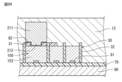
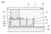
- Figures 5A to 5J correspond to the cross section taken along line II-II in Figure 1 ( Figure 2).
- the second escape wiring side is omitted from Figures 5A to 5J.
- a base insulating layer 70 that does not contain a magnetic material is formed on a substrate 90.
- the substrate 90 is made of, for example, sintered ferrite and has a flat plate shape.
- the base insulating layer 70 is made of, for example, a polyimide resin that does not contain a magnetic material.
- the base insulating layer 70 is formed by coating the polyimide resin on the substrate 90 by printing, painting, or the like. After coating, the base insulating layer 70 may be patterned using a photolithography method to leave only the polyimide resin in the area where the inductor wiring 150 is to be formed. Note that, before forming the base insulating layer 70, an insulating material that will become a grinding protection layer may be formed on the substrate 90.
- a seed layer 81 is formed on the underlying insulating layer 70.
- the material of the seed layer 81 e.g., a titanium/copper alloy
- the material of the seed layer 81 is deposited on the upper surface of the underlying insulating layer 70 by sputtering, and then patterned by photolithography to form the seed layer 81.
- a wall portion 32 that will become part of the covering insulating layer is formed on the base insulating layer 70.
- the wall portion 32 is formed, for example, from a photosensitive permanent photoresist.
- a photosensitive permanent photoresist is a photoresist that is not removed after processing. Specifically, the photosensitive permanent photoresist is laminated on the base insulating layer 70, exposed to light, and developed. This removes the material in the unexposed areas to form the wall portion 32.
- electrolytic plating is performed while power is supplied to the seed layer 81.
- the top surface portion 31 of the covering insulating layer 30 is formed on a portion of the top surface 150a of the inductor wiring 150.
- a dry film resist (DFR) is laminated on the top surface 150a of the inductor wiring 150, exposed to light, and developed. This removes the material from the portion that is not exposed to light, forming the top surface portion 31.
- the dry film resist located at the portion where the top surface 150a of the inductor wiring 150 and the second magnetic layer 12 contact each other is removed. This allows a portion of the top surface 150a of the inductor wiring 150 to come into contact with the second magnetic layer when the second magnetic layer 12 is pressure-bonded in a later process.
- a seed layer 82 is formed by sputtering so as to cover the exposed portion of the top surface 150a of the inductor wiring 150 and the top surface 31 and wall portion 32 of the covering insulating layer 30.
- the distance between the end face of the wall portion 32 of the covering insulating layer 30 and the top surface 150a of the inductor wiring 150 is 20 ⁇ m or less, the sputtered film can be adhered well even to the step portion between the upper end face of the wall portion 32 and the top surface 150a, and the seed layer 82 can be formed well.
- the first via wiring 212 and the first columnar wiring 211 are formed on the outer peripheral end 152 of the inductor wiring 150.
- a resist film 320 is formed on the seed layer 82, and an opening is provided in the resist film 320 at a position corresponding to the first via wiring 212.
- the distance between the end face of the wall portion 32 of the coating insulating layer 30 and the top surface 150a of the inductor wiring 150 is 20 ⁇ m or less, so that the resist film 320 can be formed into a desired shape.
- the first via wiring 212 and the first columnar wiring 211 can also be formed into a desired shape.
- electrolytic plating is performed while supplying power to the seed layer 82, and a plating layer is formed in the above-mentioned opening.
- the first via wiring 212 and the first columnar wiring 211 are formed in the opening.
- the resist film 320 is peeled off, the exposed seed layer 82 is removed, and the second magnetic layer 12 is pressed against the inductor wiring 150 from above the substrate 90. This causes the inductor wiring 150, the base insulating layer 70, the covering insulating layer 30, and the first columnar wiring 211 to be covered with the second magnetic layer 12.
- the top surface of the second magnetic layer 12 is ground to expose the top surface of the first columnar wiring 211.
- a coating film 60 is formed on the upper surface of the second magnetic layer 12.
- the coating film 60 is formed of, for example, solder resist.
- the substrate 90 is then ground to expose the lower surface of the base insulating layer 70.
- the first magnetic layer 11 is then pressed against the inductor wiring 150 from below the base insulating layer 70. This causes the lower surface of the base insulating layer 70 to be covered with the first magnetic layer 11.
- the lower surface of the first magnetic layer 11 is then ground to adjust the thickness of the first magnetic layer 11.
- the first external terminal 51 is then formed so as to cover the upper surface of the first columnar wiring 211.
- the first external terminal 51 has a three-layer structure of Cu/Ni/Au formed by, for example, electroless plating.
- the inductor component 1 is then manufactured by dividing the substrate 90 into individual pieces using a dicer or the like.
- Second Embodiment Fig. 6 is a schematic cross-sectional view showing a second embodiment of the inductor component.
- Fig. 6 corresponds to the cross-sectional view taken along line II-II in Fig. 1.
- the second escape wiring side is omitted in Fig. 6.
- the second embodiment differs from the first embodiment in that the top surface of the covering insulating layer and the underlying insulating layer are not provided. This different configuration will be described below.
- the other configurations are the same as those of the first embodiment, and the same reference numerals as those of the first embodiment will be used and the description thereof will be omitted.
- the covering insulating layer 30B has only a wall portion 32 and does not have a top surface portion. As a result, the entire top surface 150a of the inductor wiring 150 is in contact with the second magnetic layer 12.
- the first outgoing wiring 21B does not have a via wiring, and the first columnar wiring 211 is directly connected to the inductor wiring 150.
- the volume of the second magnetic layer 12 can be further increased, and the inductance value of the inductor component 1B can be further improved.
- inductor component 1B no underlying insulating layer is provided, and the upper surface of first magnetic layer 11 and the lower surface of second magnetic layer 12 are in contact. As a result, the entire surface of bottom surface 150b of inductor wiring 150 is in contact with first magnetic layer 11. With this configuration, the thickness of first magnetic layer 11 in the Z direction can be increased compared to when an underlying insulating layer is provided, and therefore the volume of first magnetic layer 11 can be further increased, thereby further improving the inductance value of inductor component 1B.
- the inductor component 1B can be manufactured, for example, by not providing the top surface portion 31 in the process shown in FIG. 5E, and by removing the base insulating layer 70 after grinding the substrate 90 in the process shown in FIG. 5J.
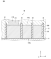
- Fig. 7 is a schematic cross-sectional view showing a third embodiment of an inductor component.
- Fig. 7 corresponds to Fig. 3.
- the third embodiment differs from the first embodiment in that a wall portion of the covering insulating layer is not provided on the inner peripheral surface of the innermost periphery of the inductor wiring.
- This different configuration will be described below.
- the other configurations are the same as those of the first embodiment, and the same reference numerals as those of the first embodiment will be used and the description thereof will be omitted.
- the innermost inner surface 150d1 of the inductor wiring 150 is in contact with the second magnetic layer 12.
- the entire innermost inner surface 150d1 of the inductor wiring 150 is in contact with the second magnetic layer 12.
- the inductor component 1C can be manufactured, for example, by not providing a wall portion 32 that corresponds to the position of the inner surface of the innermost circumference of the inductor wiring in the process shown in FIG. 5C.
- FIG. 8 is a schematic plan view showing a fourth embodiment of the inductor component.
- Fig. 8 corresponds to Fig. 1.
- the fourth embodiment differs from the first embodiment mainly in the position where the top surface of the covering insulating layer is provided. This different configuration will be described below.
- the other configurations are the same as those of the first embodiment, and the same reference numerals as those of the first embodiment are used and the description thereof will be omitted. Note that in Fig. 8, for convenience, the position where the top surface of the covering insulating layer is provided is shaded.
- the inductor wiring 150 when the direction from the bottom surface of the inductor wiring 150 toward the top surface along the axis AX is defined as a first direction, the inductor wiring 150 is connected to the top surface at the ends in the extension direction (i.e., the inner peripheral end 151 and the outer peripheral end 152), and further includes first and second outgoing wirings 21, 22 that extend in the first direction and are exposed from the outer surface of the element body 10, and the covering insulating layer 30 (i.e., the top surface portion 31) provided on a portion of the top surface of the inductor wiring 150 is separated from the first and second outgoing wirings 21, 22.
- the extension direction i.e., the inner peripheral end 151 and the outer peripheral end 152
- the covering insulating layer 30 i.e., the top surface portion 31
- the top surface 31 of the covering insulating layer 30 is provided on the entire top surface of the inductor wiring 150, excluding the areas around the first and second outgoing wirings 21 and 22.
- the top surface 31 of the covering insulating layer 30 may be provided on a part of the top surface excluding the areas around the first and second outgoing wirings 21 and 22, as long as it is separated from the first and second outgoing wirings 21 and 22.
- the first and second outgoing wirings 21 and 22 do not have the first and second via wirings 212 and 222.
- the bottom surfaces of the first and second columnar wirings 211 and 221 of the first and second outgoing wirings 21 and 22 are in direct contact with the top surface of the inductor wiring 150.
- the above configuration allows the top surface portion 31 to be provided at a desired location between the inductor wirings 150 where a short circuit is likely to occur, and since the first and second outgoing wirings 21, 22 do not have the first and second via wirings 212, 222 as shown in FIG. 1, the contact area between the first and second outgoing wirings 21, 22 (i.e., the first and second columnar wirings 211, 221) and the inductor wiring 150 can be increased, increasing the adhesion strength between the first and second outgoing wirings 21, 22 and the inductor wiring 150, and suppressing defects such as breakage due to external stress.
- first and second lead-out wiring, first and second external terminals, and a coating film are provided, but these components are not essential and may not be provided or may be replaced with other components.
- the inductor wiring is one layer, but it may be two or more layers.
- the “top surface of the inductor wiring” refers to the top surface of the inductor wiring in the topmost layer.
- the “bottom surface of the inductor wiring” refers to the bottom surface of the inductor wiring in the bottommost layer.
- the top surface of the inductor wiring is in contact with the second magnetic layer, but the entire top surface of the inductor wiring may be covered with a covering insulating layer, and at least a portion of the bottom surface of the inductor wiring may be in contact with the first magnetic layer.
- the top surface of the inductor wiring corresponds to an example of the "second surface” described in the claims
- the bottom surface of the inductor wiring corresponds to an example of the "first surface” described in the claims.
- the wall portion of the insulating coating layer is present in the entire area between adjacent turns of the inductor wiring, but the second magnetic layer may be present between adjacent turns.
- the wall portion of the insulating coating layer is provided on at least one of both side surfaces of the inductor wiring, and the second magnetic layer may be present between adjacent turns.
- Chips were fabricated in which the distance h between the top surface of the inductor wiring and the end surface in the first direction of the wall portion of the coating insulating layer was changed to 3 ⁇ m, 4 ⁇ m, 5 ⁇ m, 6 ⁇ m, 7 ⁇ m, and 10 ⁇ m, and a humidity load test was performed on each chip.
- a humidity load test a current was passed through the chip in a high-temperature and high-humidity environment, and the insulation resistance of the inductor wiring was measured after a predetermined time.
- the conditions for the humidity load test were 85° C., 85% RH, 1 A, and 500 hr. Of the 15 chips, the number of chips with normal insulation resistance (the number of good chips) was investigated. The test results are shown in Table 1.
- Chips were fabricated in which the distance h between the top surface of the inductor wiring and the end surface in the first direction of the wall of the insulating coating layer was changed to 10 ⁇ m, 15 ⁇ m, 20 ⁇ m, 25 ⁇ m, and 30 ⁇ m, and the occurrence of defects in the manufacturing process was investigated. Specifically, for samples in which a seed layer was formed by sputtering after the wall of the insulating coating layer was formed, the deposition state of the seed layer was observed using an optical microscope. In addition, for samples in which a resist film was formed after the seed layer was formed, the deposition state of the resist film was observed using an optical microscope. Then, of the 15 chips, the number of chips in which the deposition state of the seed layer and resist film was normal (number of good chips) was investigated. The investigation results are shown in Table 2.
- An element including a magnetic layer; a coil disposed within the element body and having an axis; an insulating layer covering a portion of an outer surface of the coil;
- the coil has an inductor wiring wound along a plane perpendicular to the axis, the inductor wiring has a first surface and a second surface opposed to each other in the axial direction; At least a portion of the first surface of the inductor wiring is in contact with the magnetic layer.
- the inductor wiring has two side surfaces connecting the first surface and the second surface;
- ⁇ 5> An inductor component as described in ⁇ 4>, wherein when the axial direction is a direction from the second surface of the inductor wiring toward the first surface of the inductor wiring, the end face of the wall portion in the first direction is located on the first direction side relative to the position of the first surface of the inductor wiring.
- ⁇ 6> The inductor component according to ⁇ 5>, wherein a distance in the first direction between the first surface of the inductor wiring and the end face in the first direction of the wall portion is 5 ⁇ m or more and 20 ⁇ m or less.
- the inductor wiring has two side surfaces connecting the first surface and the second surface; the two side surfaces of the inductor wiring located at the innermost periphery include an inner periphery surface of the innermost periphery and an outer periphery surface opposite to the inner periphery surface, the insulating layer has at least a wall portion provided on each of the inner circumferential surface and the outer circumferential surface,
- ⁇ 9> The inductor component according to ⁇ 8>, wherein an end face in the first direction of the wall portion provided on the inner circumferential surface is positioned on the same plane as the first surface of the inductor wiring.
- ⁇ 10> The inductor component according to any one of ⁇ 1> to ⁇ 9>, wherein the insulating layer is provided on at least a portion of the first surface of the inductor wiring.
- a first direction is a direction from the second surface to the first surface of the inductor wiring along the axial direction, the first surface being connected to an end of the inductor wiring in an extending direction thereof, the first surface being connected to an end of the inductor wiring along the axial ...
- a first direction is a direction from the second surface to the first surface of the inductor wiring along the axial direction, the first surface being connected to an end of the inductor wiring in an extending direction thereof, the first surface being connected to an end of the inductor wiring along the axial ...
Landscapes
- Engineering & Computer Science (AREA)
- Power Engineering (AREA)
- Microelectronics & Electronic Packaging (AREA)
- Coils Or Transformers For Communication (AREA)
Priority Applications (3)
| Application Number | Priority Date | Filing Date | Title |
|---|---|---|---|
| CN202380072522.XA CN120035870A (zh) | 2022-11-08 | 2023-08-10 | 电感器部件 |
| JP2024557031A JPWO2024100949A1 (https=) | 2022-11-08 | 2023-08-10 | |
| US19/195,848 US20250259785A1 (en) | 2022-11-08 | 2025-05-01 | Inductor component |
Applications Claiming Priority (2)
| Application Number | Priority Date | Filing Date | Title |
|---|---|---|---|
| JP2022-178846 | 2022-11-08 | ||
| JP2022178846 | 2022-11-08 |
Related Child Applications (1)
| Application Number | Title | Priority Date | Filing Date |
|---|---|---|---|
| US19/195,848 Continuation US20250259785A1 (en) | 2022-11-08 | 2025-05-01 | Inductor component |
Publications (1)
| Publication Number | Publication Date |
|---|---|
| WO2024100949A1 true WO2024100949A1 (ja) | 2024-05-16 |
Family
ID=91032120
Family Applications (1)
| Application Number | Title | Priority Date | Filing Date |
|---|---|---|---|
| PCT/JP2023/029300 Ceased WO2024100949A1 (ja) | 2022-11-08 | 2023-08-10 | インダクタ部品 |
Country Status (4)
| Country | Link |
|---|---|
| US (1) | US20250259785A1 (https=) |
| JP (1) | JPWO2024100949A1 (https=) |
| CN (1) | CN120035870A (https=) |
| WO (1) | WO2024100949A1 (https=) |
Citations (1)
| Publication number | Priority date | Publication date | Assignee | Title |
|---|---|---|---|---|
| JP2021136310A (ja) * | 2020-02-26 | 2021-09-13 | 株式会社村田製作所 | インダクタ部品 |
Family Cites Families (3)
| Publication number | Priority date | Publication date | Assignee | Title |
|---|---|---|---|---|
| JP6312997B2 (ja) * | 2013-07-31 | 2018-04-18 | 新光電気工業株式会社 | コイル基板及びその製造方法、インダクタ |
| JP6429609B2 (ja) * | 2014-11-28 | 2018-11-28 | Tdk株式会社 | コイル部品およびその製造方法 |
| JP7534945B2 (ja) * | 2020-12-11 | 2024-08-15 | Tdk株式会社 | コイル部品 |
-
2023
- 2023-08-10 WO PCT/JP2023/029300 patent/WO2024100949A1/ja not_active Ceased
- 2023-08-10 JP JP2024557031A patent/JPWO2024100949A1/ja active Pending
- 2023-08-10 CN CN202380072522.XA patent/CN120035870A/zh active Pending
-
2025
- 2025-05-01 US US19/195,848 patent/US20250259785A1/en active Pending
Patent Citations (1)
| Publication number | Priority date | Publication date | Assignee | Title |
|---|---|---|---|---|
| JP2021136310A (ja) * | 2020-02-26 | 2021-09-13 | 株式会社村田製作所 | インダクタ部品 |
Also Published As
| Publication number | Publication date |
|---|---|
| JPWO2024100949A1 (https=) | 2024-05-16 |
| US20250259785A1 (en) | 2025-08-14 |
| CN120035870A (zh) | 2025-05-23 |
Similar Documents
| Publication | Publication Date | Title |
|---|---|---|
| CN110136921B (zh) | 电感器部件以及其制造方法 | |
| US12033789B2 (en) | Inductor component and inductor component embedded substrate | |
| US12278039B2 (en) | Coil electronic component and method of manufacturing same | |
| US12347600B2 (en) | Inductor component and method of manufacturing inductor component | |
| US11688544B2 (en) | Inductor component | |
| US11948726B2 (en) | Inductor component | |
| US10832855B2 (en) | Electronic component and manufacturing method thereof | |
| JP2023025167A (ja) | インダクタ部品 | |
| WO2024100949A1 (ja) | インダクタ部品 | |
| CN115705948B (zh) | 电感器部件 | |
| CN112447359A (zh) | 电子部件及其制造方法 | |
| JP2021040043A (ja) | 電子部品およびその製造方法 | |
| JP7402627B2 (ja) | 基体 | |
| JP2023062559A (ja) | インダクタ部品 | |
| CN116072401B (zh) | 电感器部件以及安装部件 | |
| US20240153693A1 (en) | Inductor component | |
| JP7411590B2 (ja) | インダクタ部品およびその製造方法 | |
| JP2024068413A (ja) | インダクタ部品 | |
| JP2024058406A (ja) | インダクタ部品 | |
| JP2024108315A (ja) | コイル部品および回路基板 | |
| CN117377199A (zh) | 电子部件 |
Legal Events
| Date | Code | Title | Description |
|---|---|---|---|
| 121 | Ep: the epo has been informed by wipo that ep was designated in this application |
Ref document number: 23888304 Country of ref document: EP Kind code of ref document: A1 |
|
| WWE | Wipo information: entry into national phase |
Ref document number: 2024557031 Country of ref document: JP |
|
| WWE | Wipo information: entry into national phase |
Ref document number: 202380072522.X Country of ref document: CN |
|
| WWP | Wipo information: published in national office |
Ref document number: 202380072522.X Country of ref document: CN |
|
| NENP | Non-entry into the national phase |
Ref country code: DE |
|
| 122 | Ep: pct application non-entry in european phase |
Ref document number: 23888304 Country of ref document: EP Kind code of ref document: A1 |