WO2024095109A1 - 半導体装置および半導体装置の動作方法 - Google Patents
半導体装置および半導体装置の動作方法 Download PDFInfo
- Publication number
- WO2024095109A1 WO2024095109A1 PCT/IB2023/060832 IB2023060832W WO2024095109A1 WO 2024095109 A1 WO2024095109 A1 WO 2024095109A1 IB 2023060832 W IB2023060832 W IB 2023060832W WO 2024095109 A1 WO2024095109 A1 WO 2024095109A1
- Authority
- WO
- WIPO (PCT)
- Prior art keywords
- transistor
- signal
- layer
- wiring
- region
- Prior art date
- Legal status (The legal status is an assumption and is not a legal conclusion. Google has not performed a legal analysis and makes no representation as to the accuracy of the status listed.)
- Ceased
Links
Images



















Classifications
-
- H—ELECTRICITY
- H10—SEMICONDUCTOR DEVICES; ELECTRIC SOLID-STATE DEVICES NOT OTHERWISE PROVIDED FOR
- H10B—ELECTRONIC MEMORY DEVICES
- H10B12/00—Dynamic random access memory [DRAM] devices
-
- H—ELECTRICITY
- H10—SEMICONDUCTOR DEVICES; ELECTRIC SOLID-STATE DEVICES NOT OTHERWISE PROVIDED FOR
- H10D—INORGANIC ELECTRIC SEMICONDUCTOR DEVICES
- H10D30/00—Field-effect transistors [FET]
- H10D30/60—Insulated-gate field-effect transistors [IGFET]
- H10D30/67—Thin-film transistors [TFT]
-
- H—ELECTRICITY
- H10—SEMICONDUCTOR DEVICES; ELECTRIC SOLID-STATE DEVICES NOT OTHERWISE PROVIDED FOR
- H10D—INORGANIC ELECTRIC SEMICONDUCTOR DEVICES
- H10D84/00—Integrated devices formed in or on semiconductor substrates that comprise only semiconducting layers, e.g. on Si wafers or on GaAs-on-Si wafers
-
- H—ELECTRICITY
- H10—SEMICONDUCTOR DEVICES; ELECTRIC SOLID-STATE DEVICES NOT OTHERWISE PROVIDED FOR
- H10D—INORGANIC ELECTRIC SEMICONDUCTOR DEVICES
- H10D84/00—Integrated devices formed in or on semiconductor substrates that comprise only semiconducting layers, e.g. on Si wafers or on GaAs-on-Si wafers
- H10D84/01—Manufacture or treatment
-
- H—ELECTRICITY
- H10—SEMICONDUCTOR DEVICES; ELECTRIC SOLID-STATE DEVICES NOT OTHERWISE PROVIDED FOR
- H10D—INORGANIC ELECTRIC SEMICONDUCTOR DEVICES
- H10D84/00—Integrated devices formed in or on semiconductor substrates that comprise only semiconducting layers, e.g. on Si wafers or on GaAs-on-Si wafers
- H10D84/01—Manufacture or treatment
- H10D84/0123—Integrating together multiple components covered by H10D12/00 or H10D30/00, e.g. integrating multiple IGBTs
- H10D84/0126—Integrating together multiple components covered by H10D12/00 or H10D30/00, e.g. integrating multiple IGBTs the components including insulated gates, e.g. IGFETs
-
- H—ELECTRICITY
- H10—SEMICONDUCTOR DEVICES; ELECTRIC SOLID-STATE DEVICES NOT OTHERWISE PROVIDED FOR
- H10D—INORGANIC ELECTRIC SEMICONDUCTOR DEVICES
- H10D84/00—Integrated devices formed in or on semiconductor substrates that comprise only semiconducting layers, e.g. on Si wafers or on GaAs-on-Si wafers
- H10D84/01—Manufacture or treatment
- H10D84/02—Manufacture or treatment characterised by using material-based technologies
- H10D84/03—Manufacture or treatment characterised by using material-based technologies using Group IV technology, e.g. silicon technology or silicon-carbide [SiC] technology
- H10D84/038—Manufacture or treatment characterised by using material-based technologies using Group IV technology, e.g. silicon technology or silicon-carbide [SiC] technology using silicon technology, e.g. SiGe
-
- H—ELECTRICITY
- H10—SEMICONDUCTOR DEVICES; ELECTRIC SOLID-STATE DEVICES NOT OTHERWISE PROVIDED FOR
- H10D—INORGANIC ELECTRIC SEMICONDUCTOR DEVICES
- H10D84/00—Integrated devices formed in or on semiconductor substrates that comprise only semiconducting layers, e.g. on Si wafers or on GaAs-on-Si wafers
- H10D84/80—Integrated devices formed in or on semiconductor substrates that comprise only semiconducting layers, e.g. on Si wafers or on GaAs-on-Si wafers characterised by the integration of at least one component covered by groups H10D12/00 or H10D30/00, e.g. integration of IGFETs
- H10D84/82—Integrated devices formed in or on semiconductor substrates that comprise only semiconducting layers, e.g. on Si wafers or on GaAs-on-Si wafers characterised by the integration of at least one component covered by groups H10D12/00 or H10D30/00, e.g. integration of IGFETs of only field-effect components
- H10D84/83—Integrated devices formed in or on semiconductor substrates that comprise only semiconducting layers, e.g. on Si wafers or on GaAs-on-Si wafers characterised by the integration of at least one component covered by groups H10D12/00 or H10D30/00, e.g. integration of IGFETs of only field-effect components of only insulated-gate FETs [IGFET]
Definitions
- One aspect of the present invention relates to a semiconductor device, etc.
- one aspect of the present invention is not limited to the above technical field.
- the technical field of the invention disclosed in this specification relates to an object, a method, or a manufacturing method.
- one aspect of the present invention relates to a process, a machine, a manufacture, or a composition of matter. Therefore, more specifically, examples of the technical field of one aspect of the present invention disclosed in this specification include semiconductor devices, display devices, light-emitting devices, power storage devices, memory devices (memory devices), and their operating methods, driving methods, or manufacturing methods.
- a semiconductor device is a device that utilizes semiconductor characteristics, and refers to a circuit including a semiconductor element (transistor, diode, photodiode, etc.), a device having such a circuit, etc. Also, it refers to any device that can function by utilizing semiconductor characteristics. For example, an integrated circuit, a chip including an integrated circuit, and an electronic component that houses a chip in a package are examples of semiconductor devices. Also, memory devices, display devices, light-emitting devices, lighting devices, electronic devices, etc. may themselves be semiconductor devices and each may have a semiconductor device.
- Patent Document 1 shows an example of a CPU (Central Processing Unit) that uses power gating to reduce power consumption.
- Patent Documents 2 to 4 propose semiconductor devices that use standard cells that include Si transistors and OS transistors.
- An object of one embodiment of the present invention is to provide a novel semiconductor device or the like.
- an object of the present invention is to provide a semiconductor device or the like with reduced power consumption.
- an object of the present invention is to provide a semiconductor device or the like with high reliability.
- an object of the present invention is to provide a semiconductor device or the like that can suppress an increase in the circuit layout area.
- an object of the present invention is to provide a semiconductor device or the like with reduced power consumption.
- an object of the present invention is to provide a semiconductor device or the like with excellent computing performance.
- Another object of one embodiment of the present invention is to provide a method for operating a new semiconductor device, a semiconductor device with reduced power consumption, a highly reliable semiconductor device, a semiconductor device that can suppress an increase in the circuit layout area, a power-saving semiconductor device, or a semiconductor device with excellent computing performance.
- Another object of one aspect of the present invention is to provide a new memory device.
- Another object of one embodiment of the present invention is to provide a novel method for operating a memory device.
- problems of one embodiment of the present invention are not limited to the problems listed above.
- the problems listed above do not preclude the existence of other problems.
- the other problems are problems not mentioned in this section, which will be described below. Problems not mentioned in this section can be derived by a person skilled in the art from the description in the specification or drawings, etc., and can be appropriately extracted from these descriptions. Note that one embodiment of the present invention solves at least one of the problems listed above and/or other problems.
- One aspect of the present invention is a semiconductor device having a level shifter, a signal adjustment unit, a first register group having a plurality of first registers, and a second register group having a plurality of second registers, in which the signal adjustment unit has a first buffer circuit and a second buffer circuit, each of the plurality of first registers has a first scan flip-flop and a first memory circuit, each of the plurality of second registers has a second scan flip-flop and a second memory circuit, an output terminal of the level shifter is electrically connected to an input terminal of the first buffer circuit, an output terminal of the first buffer circuit is electrically connected to an input terminal of the second buffer circuit and the first register group, and an output terminal of the second buffer circuit is electrically connected to the input terminal of the second buffer circuit and the first register group,
- the semiconductor device is electrically connected to the group of registers, the level shifter has a function of boosting a first signal to generate a second signal and a function of outputting the second signal, the first buffer circuit has a
- the first memory circuit in each of the multiple first registers, has a first transistor including an oxide semiconductor in a semiconductor layer, and in each of the multiple second registers, the second memory circuit has a second transistor including an oxide semiconductor in a semiconductor layer, and the output terminal of the first buffer circuit is electrically connected to the gate of the first transistor in each of the multiple first registers, and the output terminal of the second buffer circuit is preferably electrically connected to the gate of the second transistor in each of the multiple second registers.
- one aspect of the present invention is a method for operating a semiconductor device having a power management unit, a signal adjustment unit, and a register group having a plurality of registers, the signal adjustment unit having a buffer circuit, a first transistor, and a second transistor, each of the plurality of registers having a scan flip-flop and a memory circuit, the method for operating a semiconductor device having a first step of starting to supply power to the buffer circuit by turning on the first transistor, a second step of the power management unit outputting a first signal to the register group via the buffer circuit and saving data held in the scan flip-flop in each of the plurality of registers to the memory circuit, a third step of providing a second signal at a low potential level to the memory circuit in each of the plurality of registers in the register group by turning on the second transistor, and a fourth step of cutting off the supply of power to the buffer circuit by turning off the first transistor.
- the memory circuit in each of the multiple registers, has a third transistor including an oxide semiconductor in a semiconductor layer, and in the third step, the second signal is preferably applied to the gate of the third transistor in the memory circuit in each of the multiple registers.
- one of the source and drain of the second transistor is electrically connected to the output terminal of the buffer circuit, and a potential that is a low potential level is applied to the other of the source and drain of the second transistor in the first step to the fourth step.
- one aspect of the present invention is a method for operating a semiconductor device having a power management unit, a signal conditioning unit, and a register group having a plurality of registers, the signal conditioning unit having a buffer circuit, a first transistor, and a second transistor, each of the plurality of registers having a scan flip-flop and a memory circuit, the method including a first step of starting to supply power to the buffer circuit by turning on the first transistor, a second step of the power management unit outputting a first signal to the register group via the buffer circuit, and in each of the plurality of registers in the register group, saving data held in the scan flip-flop to the memory circuit, and a second step of saving data to the plurality of registers in the register group by turning on the second transistor.
- a method of operating a semiconductor device includes a third step of providing a second signal at a low potential level to the memory circuit in each of the transistors, a fourth step of cutting off the supply of power to the buffer circuit by turning off the first transistor, a fifth step of starting the supply of power to the buffer circuit by turning on the first transistor, a sixth step of turning off the second transistor, a seventh step of outputting a third signal to the register group via the buffer circuit by the power management unit, and reading the data saved in the memory circuit to a scan flip-flop in each of the multiple registers in the register group, and an eighth step of cutting off the supply of power to the buffer circuit by turning off the first transistor.
- the memory circuit in each of the multiple registers included in the register group, has a third transistor including an oxide semiconductor in its semiconductor layer, a fourth transistor including an oxide semiconductor in its semiconductor layer, and a capacitor, one electrode of the capacitor is electrically connected to one of the source and drain of the third transistor and one of the source and drain of the fourth transistor, respectively, and in the third step, the first signal is provided to the gate of the third transistor included in the memory circuit in each of the multiple registers, and in the seventh step, the third signal is preferably provided to the gate of the fourth transistor included in the memory circuit in each of the multiple registers included in the register group.
- one of the source and drain of the second transistor is electrically connected to the output terminal of the buffer circuit, and a potential that is a low potential level is applied to the other of the source and drain of the second transistor in the first step to the eighth step.
- one embodiment of the present invention has a first layer and a second layer stacked on the first layer, the first layer having a functional circuit including a first region, a first wiring having a region extending in a first direction, and a second wiring having a region extending in the first direction, the functional circuit has a first transistor including silicon in a semiconductor layer, a second transistor including silicon in the semiconductor layer, and a third wiring, the first region is arranged between the first wiring and the second wiring in a top view, the first transistor has a first channel formation region and a first low resistance region functioning as one of a source and a drain, the second transistor has a second channel formation region, the first low resistance region overlaps with the third wiring, one or more of the first channel formation region and the second channel formation region are provided in the first region, the second layer has a memory circuit, and the memory circuit is arranged in the semiconductor layer.
- the semiconductor device has a third transistor including an oxide semiconductor, and the first layer or the second layer has a fourth transistor, the gate of the first transistor is electrically connected to the gate of the second transistor, one of the source and drain of the first transistor is electrically connected to the third wiring, one of the source and drain of the second transistor is electrically connected to the second wiring, the other of the source and drain of the first transistor, the other of the source and drain of the second transistor, and the gate of the third transistor are electrically connected to each other, one of the source and drain of the fourth transistor is electrically connected to the third wiring, a first high power supply potential is supplied to the first wiring, a low power supply potential is supplied to the second wiring, and a second high power supply potential higher than the first high power supply potential is supplied to the other of the source and drain of the fourth transistor.
- a first insulating layer is provided on the first low-resistance region
- a third wiring is provided on the first insulating layer
- the first low-resistance region is preferably electrically connected to the third wiring via a first plug provided in a first opening of the first insulating layer in a region overlapping with the third wiring.
- the first layer has a second functional circuit
- the second functional circuit has a second region disposed between the first wiring and the second wiring in a top view, the first region and the second region being adjacent to each other in a top view
- the second functional circuit has an element region
- the element region is electrically connected to the first wiring.
- One aspect of the present invention can provide a novel semiconductor device, etc. Or a semiconductor device, etc. with reduced power consumption can be provided. Or a highly reliable semiconductor device, etc. can be provided. Or a semiconductor device, etc. with reduced circuit layout area can be provided. Or a power-saving semiconductor device, etc. can be provided. Or a semiconductor device, etc. with excellent computing performance can be provided.
- one aspect of the present invention can provide a method for operating a novel semiconductor device, a semiconductor device with reduced power consumption, a highly reliable semiconductor device, a semiconductor device that can suppress an increase in the circuit layout area, a power-saving semiconductor device, or a semiconductor device with excellent computing performance.
- one aspect of the present invention can provide a novel storage device.
- one aspect of the present invention can provide a novel method for operating a storage device.
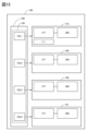
- Fig. 1A is a diagram illustrating an example of the configuration of a semiconductor device
- Fig. 1B is a diagram illustrating an example of the configuration of a register
- 2A and 2B are diagrams illustrating an example of a configuration of a semiconductor device.
- FIG. 3 is a diagram illustrating an example of a configuration of a semiconductor device.
- FIG. 4 is a diagram illustrating an example of the configuration of a register group.
- FIG. 5 is a diagram illustrating an example of a configuration of a semiconductor device.
- FIG. 6 is a diagram illustrating an example of a configuration of a semiconductor device.
- FIG. 7 is a diagram illustrating an example of a configuration of a semiconductor device.
- FIG. 8A is a diagram illustrating an example of the configuration of a register
- Fig. 8B and Fig. 8C are diagrams illustrating an example of the configuration of a CPU core.
- 9A and 9B are diagrams illustrating an example of the operation of the semiconductor device.
- Fig. 10A is a diagram illustrating an example of a configuration of a semiconductor device
- Fig. 10B and Fig. 10C are diagrams illustrating an example of a circuit.
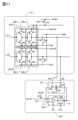
- FIG. 11 is a diagram illustrating an example of the configuration of a semiconductor device.
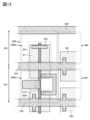
- FIG. 12 is a diagram for explaining an example of a circuit layout.
- FIG. 13 is a diagram for explaining an example of a circuit layout.
- FIG. 14 is a diagram for explaining an example of a circuit layout.
- FIG. 10A is a diagram illustrating an example of a configuration of a semiconductor device
- Fig. 10B and Fig. 10C are diagrams illustrating an example of a circuit.
- FIG. 11 is a
- FIG. 15 is a diagram illustrating a configuration example of a semiconductor device.
- FIG. 16 is a diagram illustrating an example of a configuration of a semiconductor device.
- FIG. 17 is a diagram for explaining an example of the operation of the semiconductor device.
- 18A to 18C are diagrams showing configuration examples of a semiconductor device.
- 19A to 19E are diagrams illustrating configuration examples of a semiconductor device.
- FIG. 20 is a diagram illustrating a configuration example of a semiconductor device.
- 21A and 21B are diagrams showing a configuration example of a semiconductor device.
- FIG. 22 is a diagram illustrating a configuration example of a semiconductor device.
- Fig. 23A is a diagram for explaining an example of a circuit layout
- Fig. 23B is a cross-sectional view for explaining an example of a circuit configuration.
- FIG. 24 is a cross-sectional view for explaining an example of the circuit configuration.
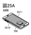
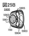
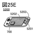
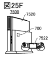
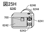
- 25A to 25J are diagrams illustrating an example of an electronic device.
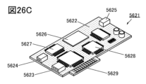
- 26A to 26C are diagrams illustrating an example of an electronic device.
- FIG. 27 is a diagram showing an example of space equipment.
- plan views also called “top views”
- oblique views some components may be omitted to make the invention easier to understand.
- Some hidden lines may also be omitted.
- the transistors shown in this specification are enhancement type (normally off type) field effect transistors.
- the threshold voltage (also referred to as "Vth") of the transistor is greater than 0V unless otherwise specified.
- the threshold voltage (also referred to as "Vth) of the transistor is less than or equal to 0V unless otherwise specified.
- the Vth of multiple transistors of the same conductivity type are all equal.
- on-current refers to the drain current (also referred to as "Id") when a transistor is in an on state (also referred to as a "conducting state”).
- the on state refers to a state in which the voltage between the gate and source (also referred to as “Vg” or “Vgs”) is Vth or higher for an n-channel transistor, and a state in which Vg is the threshold voltage or lower for a p-channel transistor.
- the on-current of an n-channel transistor may refer to the drain current when Vg is Vth or higher.
- off-state current refers to Id when a transistor is in an off state (also called a non-conducting state or a cut-off state).
- the off state refers to a state in which Vg is lower than Vth for an n-channel transistor (higher than Vth for a p-channel transistor).
- the term leakage current may be used to mean the same thing as off-state current.
- metal oxide is a metal oxide in a broad sense. Metal oxides are classified into oxide insulators, oxide conductors (including transparent oxide conductors), oxide semiconductors (also referred to as oxide semiconductors or simply OS), and the like. For example, when a metal oxide is used in the active layer of a transistor, the metal oxide may be referred to as an oxide semiconductor. In other words, when an OS transistor is described, it can be rephrased as a transistor having a metal oxide or an oxide semiconductor.
- ordinal numbers such as “first” and “second” are used to avoid confusion between components, and do not indicate any order or ranking, such as the order of processes or stacking. Even if a term does not have an ordinal number in this specification, ordinal numbers may be added in the claims to avoid confusion between components. The ordinal numbers added in this specification may differ from those added in the claims. Even if a term has an ordinal number in this specification, ordinal numbers may be omitted in the claims.
- electrode in this specification and the like do not functionally limit these components.
- electrode may be used as a part of “wiring”, and vice versa.
- the terms “electrode” and “wiring” include cases where multiple “electrodes” and “wiring” are integrated together.
- terminal may be used as a part of “wiring” or “electrode”, and vice versa.
- terminal includes cases where multiple “electrodes”, “wiring”, “terminals”, etc. are integrated together.
- an “electrode” can be a part of a “wiring” or “terminal”, and for example, a “terminal” can be a part of a “wiring” or “electrode”.
- terms such as “electrode”, “wiring”, and “terminal” may be replaced with terms such as "region” in some cases.
- supplying a signal means supplying a predetermined potential to wiring or the like. Therefore, it may be possible to read "signal” as a term such as “potential”. It may also be possible to read terms such as “potential” as a term such as “signal”. It may also be possible for a term such as “potential” to be a term such as “signal”. It may also be a variable potential or a fixed potential. For example, it may be a power supply potential.
- film and “layer” can be interchanged depending on the circumstances.
- conductive layer can be changed to the term “conductive film.”
- insulating film can be changed to the term “insulating layer.”
- the term “capacitive element” may be, for example, a circuit element having a capacitance value higher than 0F, a region of a wiring having a capacitance value higher than 0F, a parasitic capacitance, or a gate capacitance of a transistor.
- the terms “capacitive element”, “parasitic capacitance”, or “gate capacitance” may be rephrased as the term “capacitance”.
- the term “capacitance” may be rephrased as the term “capacitive element”, “parasitic capacitance”, or “gate capacitance”.
- a “capacitance” (including a “capacitance” having three or more terminals) is configured to include an insulator and a pair of conductors sandwiching the insulator. Therefore, the term “pair of conductors" in “capacitance” may be rephrased as a “pair of electrodes", a “pair of conductive regions", a “pair of regions", or a “pair of terminals”.
- the term “one of the pair of terminals” may be referred to as “one terminal” or “first terminal”.
- the term “the other of the pair of terminals” may be referred to as “the other terminal” or “second terminal”.
- the value of the electrostatic capacitance may be, for example, 0.05 fF or more and 10 pF or less. It may also be, for example, between 1 pF and 10 ⁇ F.
- source and drain of a transistor may be interchanged when transistors of different polarity are used, or when the direction of current changes during circuit operation. For this reason, in this specification, the terms “source” and “drain” can be used interchangeably.
- gate refers to a gate electrode and a part or all of a gate wiring.
- a gate wiring refers to a wiring that electrically connects the gate electrode of at least one transistor to another electrode or another wiring.
- source refers to a source region, a source electrode, and part or all of a source wiring.
- a source region refers to a region of a semiconductor layer whose resistivity is equal to or lower than a certain value.
- a source electrode refers to a conductive layer that includes a portion connected to a source region.
- a source wiring refers to wiring that electrically connects the source electrode of at least one transistor to another electrode or another wiring.
- drain refers to the drain region, drain electrode, and part or all of the drain wiring.
- the drain region refers to the region of the semiconductor layer whose resistivity is equal to or lower than a certain value.
- the drain electrode refers to the conductive layer that is connected to the drain region.
- the drain wiring refers to wiring that electrically connects the drain electrode of at least one transistor to another electrode or another wiring.
- electrode B on insulating layer A does not require that electrode B be formed in direct contact with insulating layer A, and does not exclude the inclusion of other components between insulating layer A and electrode B.
- overlap does not limit the state of the stacking order of components.
- electrode B overlapping insulating layer A does not limit the state in which electrode B is formed on insulating layer A, but does not exclude the state in which electrode B is formed under insulating layer A or the state in which electrode B is formed on the right (or left) side of insulating layer A.
- electrode B adjacent to insulating layer A does not require that insulating layer A and electrode B are formed in direct contact, and does not exclude the inclusion of other components between insulating layer A and electrode B.
- parallel refers to a state in which two straight lines are arranged at an angle of -10° or more and 10° or less. Therefore, it also includes cases in which the angle is -5° or more and 5° or less.
- substantially parallel or “roughly parallel” refers to a state in which two straight lines are arranged at an angle of -30° or more and 30° or less.
- perpendicular refers to a state in which two straight lines are arranged at an angle of 80° or more and 100° or less. Therefore, it also includes cases in which the angle is 85° or more and 95° or less.
- substantially perpendicular or “approximately perpendicular” refers to a state in which two straight lines are arranged at an angle of 60° or more and 120° or less.
- arrows indicating the X direction, Y direction, and Z direction may be attached.
- the "X direction” is the direction along the X axis, and the forward direction and the reverse direction may not be distinguished unless explicitly stated.
- the X direction, Y direction, and Z direction are directions that intersect with each other.
- the X direction, Y direction, and Z direction are directions that are perpendicular to each other.
- one of the X direction, Y direction, and Z direction may be called the "first direction” or "first direction”.
- the other one may be called the “second direction” or “second direction”.
- the remaining one may be called the "third direction” or "third direction”.
- FIG 1A is a block diagram illustrating a configuration example of a semiconductor device 100.
- the semiconductor device 100 shown in FIG. 1A has a CPU core 110, an input/output IF 140, a cache memory 150, and a state control unit 160.
- the CPU core 110 has an arithmetic unit 111, a register group 200, and a signal adjustment unit 271.
- the state control unit 160 has a PMU (Power Management Unit) 130.
- the semiconductor device 100 may also have a bus.
- the bus has a function of controlling data exchange between, for example, the CPU core 110, the PMU 130, the input/output IF 140, the cache memory 150, and the state control circuit 160.
- components of the semiconductor device 100 are not limited to those shown in FIG. 1A, and may include other components. Also, some of the components shown in FIG. 1A may be excluded. Also, one component may have the function of another component.
- the input/output IF 140 has a function of controlling the transfer of data between an external device such as a main memory (not shown) and the semiconductor device 100. Data output from the external device is input to the semiconductor device 100 via the input/output IF 140. Data output from the semiconductor device 100 is also input to the external device via the input/output IF 140.
- the cache memory 150 stores frequently used instructions and data, and has the function of reducing the frequency of access to the main memory and increasing the operating speed of the semiconductor device 100.
- the register group 200 has a function of temporarily storing data used by the CPU core 110.
- the CPU core 110 also has a function of performing arithmetic processing in the arithmetic unit 111 according to the data held in the register group 200.
- the arithmetic unit 111 has a function of performing various arithmetic processing such as arithmetic operations and logical operations.
- the arithmetic unit 111 is also called an ALU (Arithmetic Logic Unit).
- the CPU core 110 is sometimes called a processor core.
- the CPU core 110 may be configured to be provided in one semiconductor device 100 (single core), or to be provided in two or more (multi-core such as dual core or many-core).
- the register group 200 includes multiple registers 201 (register 201[1] to register 201[n], where n is an integer of 2 or more). Each register 201 may be represented as register 201[k] (k is an integer of 1 to n). Note that the register 201 is a type of memory device and also a type of semiconductor device.
- Register 201[1] functions as, for example, a program counter.
- the program counter has a function of storing a memory address indicating the next instruction to be executed.
- Register 201[2] functions as, for example, an instruction register.
- the instruction register has a function of storing an instruction read from memory.
- Register 201[3] functions as, for example, a base register.
- the base register has a function of storing the top address of the program and data stored in memory.
- Register 201[4] functions as, for example, an index register.
- the index register has a function of storing the size of data.
- Register 201[5] functions as, for example, an accumulator.
- the accumulator has a function of temporarily storing the result of the calculation performed by the calculation unit 111.
- Register 201[6] functions as, for example, a general-purpose register.
- the general-purpose register is not limited to a specific purpose and is used for various purposes.
- register 201[6] may be used as an accumulator.
- registers 201 included in the register group 200 do not have to include all of these, and may include other registers 201. Also, the register group 200 may include multiple of some or all of these registers 201. For example, the register group 200 may include multiple registers 201[6] that function as general-purpose registers.
- the signal conditioning unit 271 has a function of performing one or more of amplification, modulation, and change in potential level on the signal input to the CPU core 110.
- the signal conditioning unit 271 may also have a function of outputting the result of a calculation using the signal input to the CPU core 110.
- FIG. 1B is a block diagram showing an example of the configuration of the register 201.
- the register 201 includes a transistor 232, a scan flip-flop 220 (a volatile register), and a memory circuit 231.
- the scan flip-flop 220 has a selector 221, a flip-flop 222, a terminal D, a terminal Q, and a terminal SD.
- the terminals D and SD are each electrically connected to the selector 221, and signals input to the terminals D and SD are provided to the selector 221.
- the terminal Q is electrically connected to the flip-flop 222, and a signal output from the flip-flop 222 is provided to the terminal Q.
- the memory circuit 231 has a transistor 233, a transistor 234, and a capacitor 235.
- the state control unit 160 has a PMU 130.
- the PMU 130 is a circuit that outputs a control signal for switching between interrupt processing (also called “exception processing") and power gating in response to an interrupt signal input from the outside and a sleep signal generated by the CPU core 110.
- the state control unit 160 generates, for example, a clock signal CLK and various signals (signals BK, RE, and SE), or signals that are the basis of these various signals (for example, signals REa and BKa, which will be described later).
- the clock signal CLK and various signals are input to the CPU core 110, the input/output IF 140, the cache memory 150, and the like.
- the various signals (signals BK, RE, and SE), or signals that are the basis of these various signals are generated, for example, in the PMU 130.
- the clock signal CLK may also be generated, for example, in an area other than the state control unit 160.
- Signal BK is a signal that controls the saving of data held in flip-flop 222 in scan flip-flop 220 to memory circuit 231.
- signal BK can also be expressed as a signal that controls the saving, storing, or backing up of data held in flip-flop 222 to memory circuit 231.
- Signal RE is a signal that controls the return of data held in memory circuit 231 to flip-flop 222.
- signal RE can also be expressed as a signal that controls the loading, restoring, or recovery of data held in memory circuit 231 to flip-flop 222.
- Signal SE is a switching signal for selector 221.
- Clock signal CLK is a signal that determines the operation timing of flip-flop 222.
- Register 201 has the function of holding data input from terminal D or data input from terminal SD in scan flip-flop 220 and outputting it from terminal Q in response to clock signal CLK.
- the data of scan flip-flop 220 output from terminal Q is saved in memory circuit 231 in response to signal BK.
- the data of memory circuit 231 is loaded into scan flip-flop 220 from terminal SD of scan flip-flop 220 in response to signal RE.
- the selector 221 has a function of transmitting one of the signals input to the terminal D or the terminal SD to the flip-flop 222 in response to the signal SE.
- Data supplied from outside the register 201 is input to the terminal D.
- Data input from the memory circuit 231 or data for a scan test supplied via the terminal SD_IN is input to the terminal SD.
- the transistor 232 is provided between the terminal SD_IN and the terminal SD.
- the data for a scan test supplied via the terminal SD_IN is input to the terminal SD via the transistor 232.
- the conductive or non-conductive state of the transistor 232 is controlled by the signal BK[0].
- the flip-flop 222 is illustrated as a D flip-flop, but is not limited thereto.
- a flip-flop prepared in a standard circuit library can be applied as the flip-flop 222.
- the transistor of the flip-flop 222 is a Si transistor capable of configuring a CMOS circuit, and by having a circuit such as an inverter loop, it is possible to hold one piece of data.
- the flip-flop 222 holds data at an input terminal D F in response to a clock signal CLK, and outputs the held data from an output terminal Q F to a terminal Q.
- the memory circuit 231 is connected to a terminal Q and a terminal SD.
- a terminal electrically connected to the terminal Q is called an input terminal
- a terminal electrically connected to the terminal SD is called an output terminal.
- the output terminal QF of the flip-flop 222 is electrically connected to the input terminal of the memory circuit 231
- the input terminal DF of the flip-flop 222 is electrically connected to the output terminal of the memory circuit 231 via the terminal SD and the selector 221.
- the transistor 233 is provided between one electrode of the capacitor 235 and the terminal Q.
- the transistor 234 is provided between one electrode of the capacitor 235 and the terminal SD.
- the other electrode of the capacitor 235 is connected to the wiring CL.
- a low power supply potential, a ground potential, or the like is applied to the wiring CL.
- one electrode of the capacitor 235 is illustrated as a node SN.
- the memory circuit 231 can be said to be a nonvolatile memory.
- the memory circuit 231 rewrites data by charging and discharging the capacitor 235, so in principle there is no limit to the number of rewrites.
- data can be written and read at high speed and with low energy.
- a memory circuit configured using OS transistors is also called an "OS memory.” Therefore, the memory circuit 231 is an OS memory.
- transistors having back gates may be used for transistors 233 and 234.
- the Vth of the transistors can be controlled by supplying a constant voltage to the back gates.
- the transistor functions as a switch.
- a signal provided to the gate can be set to a high level (hereinafter also referred to as "H") to bring the source and drain into a conductive state (on state), and a signal provided to the gate can be set to a low level (hereinafter also referred to as "L") to bring the source and drain into a non-conductive state (off state).
- the selector 221 selects the signal of terminal SD by setting the signal SE to one of H and L, and selects the signal of terminal D by setting it to the other level. For example, the selector 221 selects the signal of terminal SD by setting the signal SE to a high level, and selects the signal of terminal D by setting the signal SE to a low level.
- the data held by the flip-flop 222 can be written to the node SN of the memory circuit 231. Also, by setting RE to H and SE to H, the data at the node SN of the memory circuit 231 can be written back to the flip-flop 222.
- OS transistors are a type of thin film transistor, and can be formed by stacking using existing thin film formation technology.
- the memory circuit 231 can be stacked on the scan flip-flop 220, which is configured as a CMOS circuit using Si transistors.
- an OS transistor can be preferably used as the transistor 232.
- an OS transistor By using an OS transistor, leakage current can be reduced. If the leakage current of the transistor 232 becomes large, the accuracy of the data stored in the memory circuit 231 may be reduced when the data is restored to the flip-flop 222.
- a transistor having a back gate may be used as the transistor 232. The Vth of the transistor can be controlled by supplying a constant voltage to the back gate.
- ⁇ Configuration Example 1> 2A shows an example of a configuration including the PMU 130 and the CPU core 110.
- the configuration shown in Fig. 2A also includes a level shifter LS.
- the level shifter LS is included in the state control unit 160, for example.
- the PMU 130 has the function of outputting a signal that becomes the signal RE, a signal that becomes the signal BK, and a signal that becomes the signal SE, and providing them to the CPU core 110. Note that these signals are supplied, for example, via the signal adjustment unit 271.
- signals REa and BKa are respectively provided from the PMU 130 to the level shifter LS, and are supplied to the CPU core 110 via the level shifter LS as signals REb and BKb.
- the level shifter LS has a function of, for example, boosting the H-level potential of the signal to generate a signal of the desired potential.
- FIG. 2A shows an example in which the H-level potential of the signal is boosted by the level shifter LS and input to the buffer circuit Buf
- the L-level potential of the signal may be lowered by the level shifter LS and input to the buffer circuit Buf.
- the H-level potential of the signal may be both boosted and the L-level potential may be lowered before being input to the buffer circuit Buf.
- a negative potential may be used as the L-level potential of the signal stepped down by the level shifter LS.
- the signals RE and BK are given to the gates of the transistors 234 and 233, respectively.
- the off-current can be further reduced compared to, for example, a potential of zero, and the retention characteristics of the scan flip-flop 220 can be further improved.
- the off-current can be extremely reduced by setting the gate to a negative potential.
- Signals REa and BKa are respectively supplied to the CPU core 110 as signals REb and BKb via a level shifter LS.
- Signals REb and BKb are signals in which the potential levels of signals REa and BKa are respectively changed, and here, for example, it is preferable that they are signals with an increased voltage.
- signal SE is supplied from PMU 130 to the CPU core 110.
- the OS transistor has an extremely small off-state current, and the memory circuit 231 can function as a nonvolatile memory by using the OS transistor.
- the threshold voltage of the OS transistor is preferably higher than 0 V, and thus the characteristic of the OS transistor having a small off-state current can be suitably utilized for the memory circuit 231.
- the signal REb and the signal BKb are set to signals with increased voltages, for example, the signal BK and the signal RE provided to the gates of the OS transistors 233 and 234 are set to a voltage sufficiently higher than the sum of the voltage of a high potential level (H level) signal output from the output terminal Q of the flip-flop 222 and the threshold voltage of the OS transistor, it is possible to suppress a voltage drop of the H level signal output from the output terminal Q due to the OS transistor. Therefore, the voltage of the H level signal from the output terminal Q of the flip-flop 222 can be written to the node SN without being lowered. Therefore, an improvement in the operating speed of the semiconductor device of one embodiment of the present invention is expected. Furthermore, in a semiconductor device according to one embodiment of the present invention, improved data retention characteristics and stable circuit operation are expected.
- the CPU core 110 has a number of registers 201. Signals RE, BK, SE, and a clock signal CLK are supplied to each register 201. Input data is provided to terminal D of the register 201 in each register group 200, and scan test data is provided to terminal SD via terminal SD_IN.
- the signal adjustment unit 271 is provided with a buffer circuit Buf for each of the multiple registers 201 in the CPU core 110.
- the signal REb is input to the buffer circuit Buf, output from the buffer circuit Buf as the signal RE, and supplied to the register 201.
- the signal BKb is input to the buffer circuit Buf, output from the buffer circuit Buf as the signal BK, and supplied to the register 201.
- the CPU core 110 may have a plurality of register groups 200 each consisting of a plurality of registers 201, and a buffer circuit Buf may be provided for each of the plurality of register groups 200.
- FIG. 2B shows a configuration in which the register 201 in FIG. 2A is replaced with the register group 200. The detailed configuration of the register group 200 will be described later.
- the signal REb is input to the buffer circuit Buf, output from the buffer circuit Buf as the signal RE, and supplied to the register group 200.
- the signal BKb is input to the buffer circuit Buf, output from the buffer circuit Buf as the signal BK, and supplied to the register 201.
- the buffer circuit Buf has, for example, a function to amplify and output an input signal.
- the buffer circuit Buf also has, for example, a function to divide the load capacitance.
- the signals RE and BK given to the register 201 are each given to the gate of a transistor. Therefore, an input capacitance occurs during input.
- the input capacitance of the signal RE or signal BK of the register group 200 is the product of the number of registers 201 included in the register group 200 and the input capacitance of the signal RE or signal BK of one register 201.
- the load capacitance of the output from the level shifter LS will be the sum of the input capacitances of all the registers 201 to which the wiring connected to the output terminal is electrically connected, resulting in a large load capacitance.
- the load capacitance of the output from the level shifter LS can be the input capacitance of the buffer circuit Buf, making it possible to reduce the load capacitance.
- the load capacitance of the output of the buffer circuit Buf can be the sum of the input capacitance to the register 201 to which the output terminal is connected and the input capacitance of the buffer circuit Buf in the next stage. Note that in actual operation of the circuit, parasitic capacitance of the circuit is generated in addition to the above.
- the buffer circuit Buf also has a function of shaping and outputting an input signal, for example. Specifically, for example, it can shorten the time it takes for a signal to transition from an H level to a low potential level (L level) and from an L level to an H level, thereby eliminating signal dullness. Also, by shortening the transition time, it is possible to suppress signal delay.
- L level low potential level
- the signal REb given to the CPU core 110 is propagated through wiring etc. and given to each of the register groups 200. If the distance that the signal propagates through the wiring from the input terminal of the CPU core 110 becomes long, attenuation of the potential level of the signal, rounding of the rising and falling edges of the signal, etc. may occur.
- a signal is given to multiple registers 201 (multiple register groups 200) as shown in Figures 2A and 2B, for example, the further back the register 201 (register group 200) is located, the longer the distance that the signal propagates through the wiring from the input terminal.
- the buffer circuit Buf has the function of shaping the input signal. In addition, by feeding the signal through the buffer circuit Buf, it is possible to suppress attenuation of the potential level of the signal. In addition, it is possible to make the rising and falling edges of the signal steeper.
- the CPU core 110 may supply the signal BK or signal RE to multiple register groups 200 at the same time.
- a large current flows instantaneously, causing a drop in the power supply voltage and an increase in the ground potential, which may lead to circuit malfunction.
- the timing of the signal input to the register 201 (register group 200) can be controlled.
- the signal REb is provided to the first register 201 (first register group 200) via one buffer circuit Buf.
- the signal REb is provided to the second register 201 (second register group 200) which is downstream of the first register 201 (first register group 200) via two buffer circuits Buf. Therefore, if the buffer circuit Buf has the function of delaying and outputting an input signal, for example, the signal RE provided to the downstream register 201 (register group 200) can be a signal delayed from the previous stage.
- the buffer circuit may include, for example, a circuit that has a function of outputting an inverted logic level.
- an inverter may be a type of buffer circuit.
- the inverter is, for example, a logic inversion element.
- An inverter chain consisting of multiple inverters connected in series can be used as the buffer circuit Buf.
- signals are supplied at the same time means that, for example, in an ideal state where there is no signal delay, the signals are supplied at the same time. In actual circuit operation, there may be a timing discrepancy in the time when the signals are supplied.
- the delay time between when a signal is input and when it is output can be adjusted by adjusting the number of inverter stages that are connected.
- a signal output from one level shifter LS is supplied to the multiple register groups 200.
- the number of level shifters LS in the semiconductor device 100 can be reduced, making it possible to reduce power consumption.
- the configuration shown in Fig. 3 includes transistors 242, 243, and 244. Furthermore, signals SWL and SW are supplied from the PMU 130 to the CPU core 110. Furthermore, as shown in parentheses in Fig. 3, a configuration in which a register group 200 is used instead of the register 201 can also be used.
- the transistor 242 either an n-channel transistor or a p-channel transistor may be used. As described later, a high power supply potential is applied to the transistor 242, so a p-channel transistor can be preferably used here. By using a p-channel transistor as the transistor 242, the absolute value of the potential difference between the gate and the source can be increased when the transistor operates, and the transistor can operate preferably as a switch. As the transistor 242, a Si transistor or an OS transistor may be used. When the transistor 242 is a p-channel transistor, for example, a Si transistor is used.
- n-channel transistors or p-channel transistors may be used as the transistors 243 and 244.
- n-channel transistors are used as an example.
- Si transistors or OS transistors may be used as the transistors 243 and 244.
- n-channel transistors By using n-channel transistors as the transistors 243 and 244, the absolute value of the potential difference between the gate and source can be increased when the transistors operate, and the transistors can operate suitably as switches.
- the power supply to the level shifter LS and the buffer circuit Buf of the signal adjustment unit 271 can be cut off. This makes it possible to further reduce power consumption compared to the configuration in FIG. 2A.
- a high power supply potential VDD a low power supply potential VSS (ground potential can also be used as the low power supply potential), a second high power supply potential VDDH, and the like can be used.
- the second high power supply potential VDDH is a power supply potential that is higher than the high power supply potential VDD.
- the high power supply potential VDD and the second high power supply potential VDDH can each be used as an H-level potential of a signal.
- the low power supply potential VSS can be used as an L-level potential of a signal.
- the gate of the transistor 242 is electrically connected to at least one of the wiring and terminal to which the signal SW is supplied.
- the signal SW functions as a signal for switching the transistor 242 on and off.
- One of the source and drain of the transistor 242 is electrically connected to at least one of the wiring and terminal to which the second high power supply potential VDDH is supplied.
- the other of the source and drain of the transistor 242 is electrically connected to the level shifter LS and the buffer circuit Buf of the signal adjustment unit 271.
- the power supply potential VDDHS is a power supply potential supplied to the level shifter LS and the buffer circuit Buf of the signal adjustment unit 271.
- a potential corresponding to the second high power supply potential VDDH is supplied as the power supply potential VDDHS, and the power supply of the level shifter LS and the buffer circuit Buf of the signal adjustment unit 271 is turned on.
- the power supply to the level shifter LS and the buffer circuit Buf of the signal adjustment unit 271 is cut off.
- Each of the transistors 243 and 244 is provided corresponding to one register 201 (or one register group 200).
- the signal SWL is supplied to the gates of the transistors 243 and 244.
- One of the source and drain of transistor 243 is electrically connected to the output terminal of the buffer circuit Buf from which the signal RE is output, and the other is electrically connected to at least one of the wiring and terminal to which the low power supply potential VSS is supplied.
- One of the source and drain of transistor 244 is electrically connected to the output terminal of the buffer circuit Buf from which the signal BK is output, and the other is electrically connected to a wiring to which the low power supply potential VSS is supplied.
- the potential of the output terminal of the buffer circuit Buf is no longer controlled, and the potential of the output terminal may become unstable.
- the signal RE supplied to the register 201 (or the register group 200) can be set to the L level.
- the signal BK supplied to the register group 200 can be set to L.
- Figure 4 shows an example of a circuit diagram of the register group 200.
- Figure 5 shows a block diagram in which the register 201 shown in Figure 3 is replaced with the register group 200 shown in Figure 4.
- the first register group 200 and the second register group 200 are shown as register group 200[1] and register group 200[2], respectively.
- the signals RE and BK supplied to the register group 200[1] are indicated as signals RE[1] and BK[1], respectively, and the signals RE and BK supplied to the register group 200[2] are indicated as signals RE[2] and BK[2], respectively.
- the operations of signals RE[1] and RE[2] are both synchronized with the operation of signal REb supplied to the CPU core 110.
- the operations of signals BK[1] and BK[2] are both synchronized with the operation of signal BKb supplied to the CPU core 110.
- the level shifter LS that outputs the signal REb to the CPU core 110 is represented as level shifter LS[1]. Also, the level shifter LS that outputs the signal BKb to the CPU core 110 is represented as level shifter LS[2].
- the buffer circuit Buf to which the signal REb is input from the input terminal is represented as the buffer circuit Buf[1,1].
- the buffer circuit Buf to which the signal BKb is input from the input terminal is represented as the buffer circuit Buf[2,1].
- the buffer circuit Buf to which the output from the output terminal of the buffer circuit Buf[1,1] is given is represented as the buffer circuit Buf[1,2]
- the buffer circuit Buf to which the output from the output terminal of the buffer circuit Buf[2,1] is given is represented as the buffer circuit Buf[2,2].
- the output terminal of the level shifter LS[1] is electrically connected to the input terminal of the buffer circuit Buf[1,1].
- the output terminal of the level shifter LS[2] is electrically connected to the input terminal of the buffer circuit Buf[2,1].
- the output terminal of the buffer circuit Buf[1,1] is electrically connected to the register group 200[1], and the signal RE[1] is provided from the output terminal to the register group 200[1].
- the output terminal of the buffer circuit Buf[1,1] is also electrically connected to the input terminal of the buffer circuit Buf[1,2].
- the output terminal of the buffer circuit Buf[2,1] is electrically connected to the register group 200[1], and the signal BK[1] is provided from the output terminal to the register group 200[1].
- the output terminal of the buffer circuit Buf[2,1] is also electrically connected to the input terminal of the buffer circuit Buf[2,2].
- the output terminal of the buffer circuit Buf[1,2] is electrically connected to the register group 200[2], and the signal RE[2] is provided from the output terminal to the register group 200[2].
- the output terminal of the buffer circuit Buf[2,2] is electrically connected to the register group 200[2], and the signal BK[2] is provided from the output terminal to the register group 200[2].
- transistor 243 one of whose source and drain is connected to the output terminal of buffer circuit Buf[1,1] is represented as transistor 243[1]
- transistor 244, one of whose source and drain is connected to the output terminal of buffer circuit Buf[2,1] is represented as transistor 244[1]
- transistor 243, one of whose source and drain is connected to the output terminal of buffer circuit Buf[1,2] is represented as transistor 243[2]
- transistor 244, one of whose source and drain is connected to the output terminal of buffer circuit Buf[2,2] is represented as transistor 244[2].
- a level shifter LS may be provided for each of a plurality of registers 201 included in the CPU core 110. Also, as shown in parentheses in FIG. 6, a configuration may be adopted in which a register group 200 is used instead of the register 201. That is, the CPU core 110 may have a plurality of register groups 200, and a level shifter LS may be provided for each of the register groups 200.
- the configuration shown in FIG. 6 differs from that shown in FIG. 3 in the configuration of the signal adjustment unit 271. Also, in the configuration shown in FIG. 6, a level shifter LS is not provided between the PMU 130 and the CPU core 110, and the signals REc and BKc output from the PMU 130 are supplied to the CPU core 110 without passing through the level shifter LS.
- a level shifter LS and a buffer circuit Buf are provided for each of the multiple registers 201 included in the CPU core 110.
- the signal REc is input to the buffer circuit Buf, supplied from the buffer circuit Buf to the level shifter LS, and supplied as the signal RE to the register 201 via the level shifter LS.
- the signal BKc is input to the buffer circuit Buf, supplied from the buffer circuit Buf to the level shifter LS, and supplied as the signal BK to the register 201 via the level shifter LS.
- FIG. 6 shows an example in which a power supply potential VDDS, the supply of which is controlled on and off by a transistor 245, is provided as the power supply for the buffer circuit Buf.
- the gate of the transistor 245 is electrically connected to at least one of the wiring and terminals to which a signal SW2 is supplied, one of the source and drain is electrically connected to at least one of the wiring and terminals to which a high power supply potential VDD is supplied, and the other of the source and drain has a function of supplying power to the buffer circuit Buf and is electrically connected to each of the multiple buffer circuits.
- Transistor 245 can be referred to as transistor 242.
- one of the source and drain of transistor 243 is electrically connected to the output terminal of the level shifter LS to which the signal RE is output, and the other is electrically connected to at least one of the wiring and terminals to which the low power supply potential VSS is supplied.
- one of the source and drain of transistor 244 is electrically connected to the output terminal of the level shifter LS to which the signal BK is output, and the other is electrically connected to at least one of the wiring and terminals to which the low power supply potential VSS is supplied.
- the number of level shifters LS increases. Therefore, power consumption may increase compared to the configuration shown in FIG. 3.
- the power supply to the level shifter LS can be cut off by turning off the transistor 242 using the signal SW, thereby reducing power consumption.
- each level shifter LS when a level shifter LS is provided for each register 201, the circuit size of each level shifter LS may be reduced in some cases compared to the configuration shown in FIG. 3.
- FIG. 7 shows a configuration in which the register 201 in FIG. 6 is replaced with the register group 200 shown in FIG. 4. Note that some components, such as transistor 242 and transistor 245, are omitted in FIG. 7.
- the buffer circuit Buf to which the signal REc is input from the input terminal is represented as the buffer circuit Buf_b[1,1]. Also, the buffer circuit Buf to which the signal BKc is input from the input terminal is represented as the buffer circuit Buf_b[2,1].
- the level shifter LS to which the output from the output terminal of the buffer circuit Buf_b[1,1] is given is represented as level shifter LSb[1,1]
- the buffer circuit Buf to which the output from the output terminal of the level shifter LSb[1,1] is given is represented as buffer circuit Buf[1,2]
- the level shifter LS to which the output from the buffer circuit Buf[1,2] is given is represented as level shifter LSb[1,2].
- the level shifter LS to which the output from the output terminal of the buffer circuit Buf_b[2,1] is given is represented as level shifter LSb[2,1]
- the buffer circuit Buf to which the output from the output terminal of the level shifter LSb[2,1] is given is represented as buffer circuit Buf[2,2]
- the level shifter LS to which the output from the buffer circuit Buf[2,2] is given is represented as level shifter LSb[2,2].
- the output terminal of the level shifter LSb[1,1] is electrically connected to the register group 200[1], and the signal RE[1] is provided from the output terminal to the register group 200[1].
- the output terminal of the level shifter LSb[2,1] is electrically connected to the register group 200[1], and the signal BK[1] is provided from the output terminal to the register group 200[1].
- the output terminal of the level shifter LSb[1,2] is electrically connected to the register group 200[2], and the signal RE[2] is provided from the output terminal to the register group 200[2].
- the output terminal of the level shifter LSb[2,2] is electrically connected to the register group 200[2], and the signal BK[2] is provided from the output terminal to the register group 200[2].
- transistor 243 one of whose source and drain is connected to the output terminal of level shifter LSb[1,1] is represented as transistor 243b[1]
- transistor 243, one of whose source and drain is connected to the output terminal of level shifter LSb[1,2] is represented as transistor 243b[2]
- transistor 244b[2 one of whose source and drain is connected to the output terminal of level shifter LSb[2,2] is represented as transistor 244b[2].
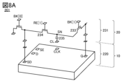
- a layer 20 including a circuit including an OS transistor can be stacked over a layer 10 including a circuit including a Si transistor.
- Figure 8A shows a configuration example of a register 201 included in a semiconductor device of one embodiment of the present invention.
- a memory circuit 231 can be stacked on a scan flip-flop 220 that is configured as a CMOS circuit using Si transistors.
- This configuration allows multiple memory circuits 231 to be provided within the area in which the scan flip-flops 220 are formed, so even if multiple memory circuits 231 are incorporated, the area overhead of the register 201 can be made essentially zero.
- Figure 8B shows an example of a configuration in which the CPU core 110 is provided in layer 10 and layer 20.
- the components of the register group 200 are provided in each of layer 10 and layer 20.
- the register group 200 has, for example, multiple registers 201 provided in layer 10 and layer 20 as shown in Figure 8A.
- the components of the calculation unit 111 may be provided in layer 10, may be provided in each of layer 10 and layer 20, or may be provided in layer 20.
- FIG. 8B shows an example in which the signal adjustment unit 271 is provided in the layer 10.
- the signal adjustment unit 271 can be configured using, for example, a Si transistor. Note that the region in the layer 10 in which the signal adjustment unit 271 is provided may overlap the region in the layer 20 in which the register 201 is provided.
- components of the signal adjustment unit 271 may be provided in each of the layers 10 and 20.
- OS transistors provided in the layer 20 may be used as the transistors 243 and 244.
- the transistor 242 is a p-channel transistor, for example, a Si transistor provided in the layer 10 may be used as the transistor 242.
- the buffer circuit Buf may be provided in the layer 10 or in the layer 20. Alternatively, the buffer circuit Buf may be configured using semiconductor elements provided in each of the layers 10 and 20.
- a level shifter LS having a function of changing the voltage levels of signals REa and BKa, etc., output from PMU 130 may be provided in layer 10 or layer 20. Alternatively, it may be configured using semiconductor elements that each of layer 10 and layer 20 has.
- Fig. 9A is a timing chart showing an example of the operation of a semiconductor device of one embodiment of the present invention, in which the horizontal axis indicates the passage of time. Also, 110 (core) corresponds to the operation of the CPU core 110.
- the transistor 242 is turned on to start supplying power to the level shifter LS and the buffer circuit Buf.
- the signal SW provided to the gate of the transistor 242 is set to a potential that turns the transistor 242 on, causing the power supply potential VDDHS to rise from the L level to the H level.
- the H level of the power supply potential VDDHS is, for example, the second high power supply potential VDDH.
- a signal to execute power gating is supplied from PMU 130 to CPU core 110. Specifically, signals REa and SE remain at L level, BKa is set to H level, and then at time Tc, signal BKa is set to L level.
- the data held in scan flip-flops 220 in each of the multiple registers 201 of register group 200 is saved to memory circuit 231.
- a signal BKa is provided to multiple register groups 200 at time Tb.
- a large current flows instantaneously, which can cause a drop in the power supply voltage, an increase in the ground potential, and other problems that can lead to circuit malfunction.
- a signal is provided to the register group 200 via a buffer circuit Buf, which can suppress signal delays, changes in the signal waveform, and the like.
- the power supply can be stopped for the entire CPU core 110 or for part of it.
- Time Tc is, for example, one clock after time Tb.
- Data can be evacuated in one clock operation, allowing for quick data evacuation.
- signal SWL is set to a potential at which transistors 243 and 244 are turned on.
- signal SWL is set to H level.
- transistors 243 and 244 of signal adjustment unit 271 are turned on, and signals RE and BK supplied to each of multiple register groups 200 are turned to L level.
- signals RE and BK can be held at L level even after power supply to buffer circuit Buf is cut off.
- the power supply to the CPU core 110 is cut off. Specifically, for example, the power supply to the register group 200, the arithmetic unit 111, etc. is cut off.
- the signal SW provided to the gate of the transistor 242 is set to a potential that turns off the transistor 242, and the power supply potential VDDHS drops from the H level to the L level. This cuts off the power supply to the level shifter LS and the buffer circuit Buf.
- the signal SW given to the gate of the transistor 242 is first set to a potential that turns on the transistor 242, and the power supply potential VDDHS rises from the L level to the H level. This supplies power to the level shifter LS and the buffer circuit Buf.
- signal SWL is set to a potential at which transistors 243 and 244 are turned off.
- signal SWL is set to the L level.
- signal BKa remains at L level, and signals REa and SE are set to H level, and then at time Tk, signals REa and SE are set to L level, whereby in the multiple register groups 200 of the CPU core 110, the data held in the memory circuit 231 in each of the multiple registers 201 of the register group 200 is loaded into the scan flip-flop 220.
- the signal SW provided to the gate of the transistor 242 is set to a potential that turns the transistor 242 off, and the power supply potential VDDHS drops from H level to L level. This cuts off the power supply to the level shifter LS and the buffer circuit Buf, and during the period when no data is held in the memory circuit 231 in the register 201, the power consumption of the signal adjustment unit 271 can be reduced.
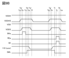
- FIG 9B illustrates an example of the operation of the configuration illustrated in FIG 7.
- FIG 9B is a timing chart illustrating an example of the operation of the semiconductor device of one embodiment of the present invention, in which the horizontal axis indicates the passage of time.
- 110 core
- 110 corresponds to the operation of the CPU core 110.
- FIG. 9B the operation of the high power supply potential VDD and the power supply potential VDDS is shown. Also, the operation of the second high power supply potential VDDH, the power supply potential VDDHS, the signal BKa, the signal REa, the signal SE, the CPU core 110, and the signal SWL shown in FIG. 9B can be seen in FIG. 9A.
- Time Ta' is, for example, one clock after time Ta.
- Time Te' is, for example, one clock before time Tf.
- Time Tg' after time Tg, the signal SW2 provided to the gate of transistor 245 is set to a potential that turns on transistor 245, causing the power supply potential VDDHS to rise from the L level to the H level.
- Time Tg' is, for example, one clock after time Tg.
- time Tk the signal SW2 provided to the gate of transistor 245 is set to a potential that turns off transistor 245, and the power supply potential VDDS drops from H level to L level. This cuts off the power supply to the buffer circuit Buf.
- time Tk is, for example, one clock before time Tm.
- Figure 10A shows the configuration example of the CPU core 110 shown in Figure 8C again, and also shows an enlarged view of a portion of layer 10 (hereinafter, area 510).
- the layer 10 shown in FIG. 8A to FIG. 8C can be provided with a functional circuit of one embodiment of the present invention.
- a functional circuit is provided in a region of the layer 10 of the signal adjustment portion 271
- FIG. 10A shows an example in which a region 510 is provided as a circuit region including a functional circuit 500 in the region of the layer 10 in the signal adjustment portion 271 shown in FIG. 8C, but a circuit region including a functional circuit 500 may be provided in the signal adjustment portion 271 of the layer 10 shown in FIG. 8B.
- the circuit region including the functional circuit 500 is not limited to these examples, and a circuit region including a functional circuit 500 can be provided as appropriate in a circuit or the like included in a semiconductor device of one embodiment of the present invention.
- VDD wiring 523 and VSS wiring 524 are arranged alternately in region 510.
- a functional circuit 500 can be provided in region 510.
- VDDHS wiring 525 is provided in the functional circuit 500.
- the VDD wiring 523 is, for example, a wiring including a region extending in one direction
- the VSS wiring 524 is, for example, a wiring including a region extending in the same direction as the VDD wiring 523.
- the functional circuit 500 has a region 500a sandwiched between the VDD wiring 523 and the VSS wiring 524.
- the functional circuit 500 has a region 500a sandwiched between the VDD wiring 523 and the VSS wiring 524 located below the VDD wiring 523 in a top view.
- the VDD wiring 523 and the VSS wiring 524 are arranged in parallel.
- the VSS wiring 524 located below the VDD wiring 523 is provided in a position facing the VDD wiring 523 across the region 500a.
- the VDD wiring 523 is arranged between two VSS wirings 524 (the first VSS wiring 524 and the second VSS wiring 524).
- the functional circuit 500 has a region 500a sandwiched between the VDD wiring and the first VSS wiring 524, and a region 500b sandwiched between the VDD wiring and the second VSS wiring 524.
- the functional circuit 500 has a region 500b sandwiched between the VDD wiring 523 and the VSS wiring 524 located above the VDD wiring 523 in a top view.
- the VSS wiring 524 located above the VDD wiring 523 is provided in a position facing the VDD wiring 523 across the region 500b.
- the VDD wiring 523 is a wiring to which a high power supply potential VDD is supplied.
- the VSS wiring 524 is a wiring to which a low power supply potential VSS is supplied.
- the VDDHS wiring 525 is a wiring to which a power supply potential VDDHS based on a second high power supply potential VDDH is supplied.
- Standard cells can be suitably arranged in the region where VDD wiring 523 and VSS wiring 524 are alternately arranged as shown in FIG. 10A.
- the standard cells can be configured, for example, by combining an element region provided in a semiconductor layer with a conductive layer that functions as wiring, a plug, a terminal, an electrode, etc.
- the semiconductor layer can be electrically connected to an upper conductive layer via a plug or the like.
- the element region provided in the semiconductor layer has elements such as transistors, capacitance elements, diodes, etc.
- the element region has, for example, a semiconductor region, a low resistance region, etc. For the semiconductor region and the low resistance region, for example, refer to FIG. 22 described below.
- a standard cell is a functional circuit with a specific pre-designed function.
- a semi-custom IC is a circuit created using a library of standard cells. By using standard cells, semiconductor devices can be easily designed by placing multiple standard cells in the circuit design of the semiconductor device and connecting each standard cell with wiring, etc.
- the functional circuit 500 shown in FIG. 10A can be used as a standard cell.
- the functional circuit 500 shown in FIG. 10A has an element region 511 and an element region 512.
- FIG. 10A shows an example in which functional circuits 901, 902, etc. are placed adjacent to the functional circuit 500.
- the functional circuits 901 and 902 are standard cells.
- the functional circuits 901 and 902 are functional circuits having element regions 561, 562, etc. Note that in FIG. 10A and other figures, for ease of viewing, a gap is shown between adjacent functional circuits, but when standard cells are used as each functional circuit, for example, it is preferable that the standard cells are placed without gaps.
- an element isolation region is provided at the boundary between the standard cells, so that adjacent standard cells can be placed without gaps.
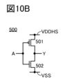
- Figure 10B is a circuit diagram of the functional circuit 500.
- the functional circuit 500 can function as an inverter.
- the functional circuit 500 has an input terminal A and an output terminal Y.
- FIG. 12 is a top view showing a layout of a circuit of one embodiment of the present invention, which is a further specific example of FIG. 10(A).
- the top view shown in FIG. 12 includes wirings such as a wiring 522, a wiring 528, and a wiring 527 in addition to the configuration shown in FIG. 10(A).
- the functional circuit 500 shown in FIG. 12 can be used as a standard cell.
- the wiring 527 functions as, for example, an input terminal A in the circuit diagram shown in FIG. 10(B).
- the wiring 527 is electrically connected to a conductive layer that functions as an input terminal A in the circuit diagram shown in FIG. 10(B).
- the wiring 528 functions as an output terminal Y in the circuit diagram shown in FIG. 10(B).
- the wiring 528 is electrically connected to a conductive layer that functions as an output terminal Y in the circuit diagram shown in FIG. 10(B).
- the functional circuit 500 shown in Figs. 10A and 12 can be applied to, for example, the buffer circuit Buf shown in the previous embodiment. It is preferable to use a configuration in which a plurality of functional circuits 500 shown in Figs. 10B and 12 are connected in series as the buffer circuit Buf shown in the previous embodiment. By connecting an even number of functional circuits 500, it is possible to output a non-inverted signal input to the buffer circuit.
- a circuit diagram of a buffer circuit Buf in which two functional circuits 500 are connected is shown in Fig. 10C.
- Figure 11 shows a configuration in which the buffer circuit Buf shown in Figure 10C is applied to the CPU core 110 shown in Figure 3. Note that some components are omitted in Figure 11.
- FIG. 11 shows a buffer circuit Buf (shown as buffer circuit Buf[1] in FIG. 11) that provides a signal RE to the register 201, and a buffer circuit Buf (shown as buffer circuit Buf[2] in FIG. 11) that provides a signal BK.
- the buffer circuit Buf[1] and the buffer circuit Buf[2] each have a first-stage functional circuit 500 (shown as functional circuit 500_1 in FIG. 11) and a second-stage functional circuit 500 (shown as functional circuit 500_2 in FIG. 11).
- One of the source and drain of transistor 242 is electrically connected to at least one of the wiring and terminal to which the second high power supply potential VDDH is supplied.
- each functional circuit 500 (functional circuit 500_1, functional circuit 500_2) shown in FIG. 11, one of the source and drain of transistor 501 is electrically connected to the other of the source and drain of transistor 242, and one of the source and drain of transistor 502 is electrically connected to at least one of the wiring and terminal to which the low power supply potential VSS is supplied.
- the output from the functional circuit 500_2 in the buffer circuit Buf[1] is provided as a signal RE to the transistor 234 in the register 201.
- the other of the source and drain of the transistor 501 and the other of the source and drain of the transistor 502 are electrically connected to the gate of the transistor 234 in the register 201.
- the output from the functional circuit 500_2 in the buffer circuit Buf[2] is provided as a signal BK to the transistor 233 in the register 201.
- the other of the source and drain of the transistor 501 and the other of the source and drain of the transistor 502 are electrically connected to the gate of the transistor 233 in the register 201.
- the functional circuit 500 shown in FIG. 12 has a gate wiring 522, a VDD wiring 523, a VSS wiring 524, a VDDHS wiring 525, wiring 527, and wiring 528.
- FIG. 12 also shows an element region 511 and an element region 512 in which a channel formation region of a transistor, a low resistance region, etc. are provided.
- the element region 511 is a region in which, for example, a p-channel transistor is provided, and includes, for example, a p-type low resistance region formed by adding impurities to a semiconductor layer.
- the element region 512 is a region in which, for example, an n-channel transistor is provided, and includes, for example, an n-type low resistance region formed by adding impurities to a semiconductor layer.
- the functional circuit 500 shown in FIG. 12 has a transistor 501 and a transistor 502 arranged between a VDD wiring 523 and a VSS wiring 524.
- the channel formation region, low resistance region, etc. of the transistor 501 can be provided in the element region 511.
- the channel formation region, low resistance region, etc. of the transistor 502 can be provided in the element region 512.
- the gate wiring 522 functions as a gate electrode for transistors 501 and 502.
- the opening 542 is an opening provided in the insulator between the VDDHS wiring 525 and the element region 511, and a plug or the like can be provided in the opening.
- One of the source and drain of the transistor 501 can be electrically connected to the VDDHS wiring 525 via the plug.
- the VDDHS wiring 525 is preferably electrically connected to the transistor 242 described in the previous embodiment.
- the VDDHS wiring 525 is, for example, electrically connected to one of the source and drain of the transistor 242.
- the VDDHS wiring 525 is electrically connected to a conductive layer such as an electrode or wiring provided above the VDDHS wiring 525 via a plug or the like, and is electrically connected to one of the source and drain of the transistor 242 via the conductive layer.
- the opening 548 is an opening provided in the insulator between the VSS wiring 524 and the element region 512, and a plug or the like can be provided in the opening.
- One of the source and drain of the transistor 502 can be electrically connected to the VSS wiring 524 via the plug.
- Opening 543 is an opening provided in the insulator between wiring 528 and element region 511, and a plug or the like can be provided in the opening.
- Opening 546 is an opening provided in the insulator between wiring 528 and element region 512, and a plug or the like can be provided in the opening.
- the other of the source and drain of transistor 501 can be electrically connected to the other of the source and drain of transistor 502 via the plug provided in opening 543, the plug provided in opening 546, and wiring 528.
- the opening 544 is an opening provided in the insulator between the gate wiring 522 and the wiring 527, and a plug or the like can be provided in the opening.
- the wiring 527 and the gate wiring 522 can be electrically connected via the plug.
- the functional circuit 500 is arranged across two regions, a region 551 and a region 552 located adjacent to the region 551 in the top view.
- the region 551 is between the VSS wiring 524 and the VDD wiring 523 located adjacent to the VSS wiring 524 in the top view
- the region 552 is between the VDD wiring 523 and the VSS wiring 524 located adjacent to the VDD wiring 523 in the top view.
- the region provided in the region 551 is referred to as region 500a
- region 500b shown in FIG. 13 described below.
- FIG. 13 shows a layout diagram including a functional circuit 500 and an area adjacent to the functional circuit.
- functional circuits 901 and 902 are arranged in an area adjacent to the functional circuit 500.
- the functional circuit 901 has an element region 561 and an element region 562.
- the functional circuit 902 has an element region 561.
- the element region 561 has an area included in the functional circuit 901 and an area included in the functional circuit 902, with a wiring 523 sandwiched between them.
- the element region 561 and the element region 562 are provided in a semiconductor layer.
- the element region 561 has a low resistance region electrically connected to, for example, the VDD wiring 523.
- the element region 562 has a low resistance region electrically connected to the VSS wiring 524.
- a transistor can be provided in each of the element region 561 and the element region 562.
- a gate wiring can be provided overlapping the element region 561.
- element region 511, element region 512, element region 561, and element region 562 are provided in a layer containing silicon, for example.
- the functional circuit 500 can be used as a buffer circuit included in a semiconductor device of one embodiment of the present invention.
- a configuration in which multiple stages of the functional circuits 500 are connected in series can be used as a buffer circuit included in a semiconductor device of one embodiment of the present invention.
- the functional circuit 500 can be constructed by adding a VDDHS wiring 525 in addition to the VDD wiring 523 and the VSS wiring 524, and can be provided between the VDD wiring 523 and the VSS wiring 524 as shown in the top views of Figures 12 and 13. This has the advantage that it can be easily arranged alongside other standard cells provided between the VDD wiring 523 and the VSS wiring 524, and it can be easily incorporated into a circuit area configured using standard cells, which increases the degree of freedom in arrangement when designing a circuit.
- FIG. 14 also shows a layout of the functional circuit 500 different from that shown in FIG. 12.
- the functional circuit 500 shown in FIG. 14 is provided in an area 551. Since the functional circuit 500 shown in FIG. 14 can be placed only in the area 551, other functional circuits can be placed in the area 552, for example.
- Another functional circuit 500 may be placed in the area 552, and two functional circuits 500 may be placed side by side in the vertical direction in FIG. 14.
- two functional circuits 500 may be placed in the areas 551 and 552 with the VDD wiring 523 between them.
- the VDD wiring 523 and the VSS wiring 524 extend in the horizontal direction. Therefore, the vertical direction in FIG. 14 is a direction perpendicular to the direction in which the VDD wiring 523 and the VSS wiring 524 extend.
- the semiconductor device 100 preferably has a function of individually power gating each block (a semiconductor device such as a CPU or a peripheral circuit).
- Each block preferably has the register group 200 and signal adjustment unit 271 described above.
- FIG. 15 shows an example in which PMU 130 has multiple blocks (four blocks: PMU block 130_1, PMU block 130_2, PMU block 130_3, and PMU block 130_4) corresponding to the respective blocks.
- PMU 130_1 provides a signal to CPU core 110
- PMU 130_2 and PMU 130_3 provide signals to I/O IF 140 (first I/O IF 140 and second I/O IF 140), respectively
- PMU 130_4 provides a signal to memory 151.
- memory 151 may be, for example, an external main memory or a memory included in semiconductor device 100.
- the input/output IF 140 (first input/output IF 140 and second input/output IF 140) and memory 151 each have a signal adjustment unit and a register group.
- the configuration, function, etc. of the signal adjustment unit and register group of the input/output IF 140 (first input/output IF 140 and second input/output IF 140) and memory 151 can be referred to the signal adjustment unit 271 and register group 200 of the CPU core 110, respectively, and in FIG. 15, the same reference numerals are used as the signal adjustment unit 271 and register group 200 of the CPU core 110.
- Figure 16 shows an excerpt of the configuration shown in Figure 15, including the CPU core 110, the input/output IF 140 (first input/output IF 140), and the PMU block 130_1 and PMU block 130_2 connected to each of them.
- Figure 3 and other figures can be referenced for the configuration of the signal adjustment unit 271.
- Figure 4 and other figures can be referenced for the register group 200.
- Signals SW, SWL, and SE are supplied from the PMU block 130_1 to the CPU core 110.
- signals REa and BKa are each supplied from the PMU block 130_1 to the CPU core 110 via a level shifter LS.
- the signals SW_2, SWL_2, and SE_2 are supplied from the PMU block 130_2 to the input/output IF 140 (first input/output IF 140).
- the signals REa_2 and BKa_2 are each supplied from the PMU block 130_2 to the input/output IF 140 (first input/output IF 140) via the level shifter LS.
- the signal adjustment unit 271 of the input/output IF 140 (first input/output IF 140) has a transistor 242, a transistor 243 (not shown), a transistor 244 (not shown), a plurality of buffer circuits Buf (not shown), and the like.
- the gate of the transistor 242 is electrically connected to at least one of the wiring and terminal to which the signal SW_2 is supplied.
- One of the source and drain of the transistor 242 is electrically connected to at least one of the wiring and terminal to which the second high power supply potential VDDH is supplied.
- a potential corresponding to the second high power supply potential VDDH is supplied as the power supply potential VDDHS_2, and by turning it off, the supply of power to the level shifter LS and the buffer circuit Buf of the signal adjustment unit 271 is cut off.
- Fig. 17 is a timing chart showing an operation example of a semiconductor device of one embodiment of the present invention, in which the horizontal axis indicates the passage of time (Time). Also, 110 (core) corresponds to the operation of the CPU core 110, and 140 (IF) corresponds to the operation of the input/output IF 140 (first input/output IF 140).
- the signal SW_2 provided to the gate of the transistor 242 of the signal adjustment unit 271 of the input/output IF 140 (first input/output IF 140) is set to a potential that turns the transistor 242 on, thereby causing the power supply potential VDDHS_2 to rise from the L level to the H level.
- signals REa_2 and SE_2 remain at L level, and signal BKa_2 is set to H level. Thereafter, at time T9, signal BKa_2 is set to L level.
- the data held in the scan flip-flop 220 in each of the multiple registers 201 of the register group 200 is saved to the memory circuit 231.
- Time T9 is, for example, one clock after time T8.
- signal SWL_2 is set to a potential that turns on transistors 243 and 244 (not shown) of signal adjustment unit 271 of input/output IF 140 (first input/output IF 140).
- signal SWL_2 is set to H level. This allows signals RE and BK to be held at L level even after the power supply to buffer circuit Buf is cut off.
- the power supply to the input/output IF 140 (first input/output IF 140) is cut off. Specifically, for example, the power supply to the register group 200, the calculation unit 111, etc. is cut off.
- the signal SW provided to the gate of the transistor 242 in the signal adjustment unit 271 of the input/output IF 140 is set to a potential that turns the transistor 242 off, and the power supply potential VDDHS drops from the H level to the L level. This cuts off the power supply to the level shifter LS and the buffer circuit Buf.
- Figure 18A is a plan view of a configuration including a memory circuit 231, which is a type of semiconductor device, as viewed from the Z direction.
- Figure 18B is a cross-sectional view of the portion indicated by the dashed line A1-A2 in Figure 18A as viewed from the Y direction.
- Figure 18C is a cross-sectional view of the portion indicated by the dashed line A3-A4 in Figure 18A as viewed from the X direction. Note that in the plan view of Figure 18A, some elements have been omitted for clarity. Note that in this embodiment and other cases, the stacking direction of the layers that make up the semiconductor device is the Z direction.
- the memory circuit 231 includes a transistor 233, a transistor 234, and a capacitor 235.
- the conductive layer 361 and the conductive layer 355 function as one and the other of the source or drain electrodes of the transistor 234.
- the transistor 233 has a similar structure to the transistor 234 and is formed at the same time as the transistor 234.
- the conductive layer 355 and the conductive layer 351 function as one and the other electrodes of the capacitor 235, respectively, and the insulating layer 354 functions as a dielectric of the capacitor 235.
- the configuration shown in Figures 18A to 18C has an insulating layer 353, and conductive layers 351 and 352 formed to be embedded in the insulating layer 353.
- the conductive layers 351 and 352 can be formed simultaneously in the same manufacturing process using the same material. It is also preferable to use a chemical mechanical polishing (CMP) method or the like to make the positions (positions in the Z direction) of the upper surfaces of the insulating layer 353, the conductive layer 351, and the conductive layer 352 coincide or approximately coincide.
- CMP chemical mechanical polishing
- an insulating layer 354 is provided on the insulating layer 353, the conductive layer 351, and the conductive layer 352, and a conductive layer 355 is provided on the insulating layer 354.
- the conductive layer 351 and the conductive layer 355 have an overlapping region with the insulating layer 354 interposed therebetween.
- It also includes a conductive layer 351, a conductive layer 355, and an insulating layer 354.
- a material with a high relative dielectric constant (also referred to as a "high-k material”) may be used for the insulating layer 354, which functions as a dielectric of the capacitor 235.
- a high-k material As the insulating layer 354, the electrostatic capacitance required for the capacitor 235 can be secured and the insulating layer 354 can be made thicker.
- the dielectric strength between the conductive layer 351 and the conductive layer 355 is increased, and electrostatic breakdown is suppressed. This improves the reliability of the capacitor 235. This improves the reliability of a semiconductor device using the capacitor 235.
- a ferroelectric may be used for the insulating layer 354 that functions as the dielectric of the capacitive element 235.
- a ferroelectric has the property that polarization occurs inside when an electric field is applied from the outside, and the polarization remains even when the electric field is made zero. For this reason, a non-volatile memory element can be realized by using a capacitive element that uses this material as a dielectric (also called a "ferroelectric capacitor").
- 18A to 18C has an insulating layer 357 on the insulating layer 354 and the conductive layer 355, an insulating layer 358 on the insulating layer 357, and an insulating layer 359 on the insulating layer 358.
- the insulating layer 357, the insulating layer 358, and the insulating layer 359 may be collectively referred to as an insulating layer 356 or a spacer layer.
- the memory circuit 231 has a conductive layer 361 on the insulating layer 359.
- an opening 362 is provided in the conductive layer 361, the insulating layer 359, the insulating layer 358, and the insulating layer 357 in a region overlapping with a part of the conductive layer 355.
- the memory circuit 231 shown in FIG. 18A to FIG. 18C has a semiconductor layer 363 that covers the opening 362.
- the semiconductor layer 363 has a region that overlaps with the bottom of the opening 362 and a region that overlaps with the side of the opening 362. That is, the semiconductor layer 363 has a region in contact with the insulating layer 356.
- the semiconductor layer 363 has a region in contact with the side of the insulating layer 357, a region in contact with the side of the insulating layer 358, and a region in contact with the side of the insulating layer 359.
- the semiconductor layer 363 also has a region in contact with the conductive layer 355 and a region in contact with the conductive layer 361. That is, a part of the semiconductor layer 363 is electrically connected to the conductive layer 355, and another part of the semiconductor layer 363 is electrically connected to the conductive layer 361.
- the semiconductor layer 363 may also have a region that extends beyond the end of the conductive layer 361 (see Figures 18A and 18C).
- an insulating layer 364 is provided on the insulating layer 359, the conductive layer 361, and the semiconductor layer 363.
- a conductive layer 365 is provided on the insulating layer 364. In FIG. 18A, the conductive layer 365 extends in the Y direction.
- the insulating layer 364 and the conductive layer 365 each have an area that overlaps with the opening 362.
- the insulating layer 364 has an area that overlaps with the side of the conductive layer 361 via the semiconductor layer 363, and an area that overlaps with the side of the insulating layer 356 (insulating layer 359, insulating layer 358, and insulating layer 357).
- the conductive layer 365 has an area that overlaps with the side of the opening 362 (the side of the insulating layer 356) via the insulating layer 364 and the semiconductor layer 363.
- the thickness of the semiconductor layer 363 is preferably 1 nm or more, 3 nm or more, or 5 nm or more, and 20 nm or less, 15 nm or less, 12 nm or less, or 10 nm or less.
- the thickness of the insulating layer 364 is preferably 0.5 nm or more and 15 nm or less, more preferably 0.5 nm or more and 12 nm or less, and even more preferably 0.5 nm or more and 10 nm or less. It is sufficient that at least a portion of the insulating layer 364 has a region with the above-mentioned thickness.
- an insulating layer 366 is provided on the insulating layer 364 (see FIG. 18B). It is preferable that the positions (positions in the Z direction) of the upper surfaces of the conductive layer 365 and the insulating layer 366 are made to coincide or approximately coincident. For example, it is preferable that the positions of the upper surfaces of the conductive layer 365 and the insulating layer 366 are made to coincide or approximately coincident by performing a CMP process or the like. By making the positions of the upper surfaces of the conductive layer 365 and the insulating layer 366 coincide or approximately coincident, the coverage of the insulating layer and the conductive layer formed later can be improved.
- an insulating layer 367 is provided on the conductive layer 365 and the insulating layer 366.
- a conductive layer 368 is provided so as to be embedded in a portion of the insulating layer 367, the insulating layer 366, the insulating layer 364, the conductive layer 361, the insulating layer 359, the insulating layer 358, the insulating layer 357, and the insulating layer 354.
- the conductive layer 368 is electrically connected to the conductive layer 361 and the conductive layer 352.
- the conductive layer 368 and the conductive layer 352 function as contact plugs.
- the conductive layer 361 functions as one of the source electrode and the drain electrode of the transistor 234.
- the conductive layer 355 functions as the other of the source electrode and the drain electrode of the transistor 234.
- the conductive layer 355 functions as the source electrode of the transistor 234.
- the transistor 234 is formed in a region overlapping with the conductive layer 355.
- the semiconductor layer 363 functions as a semiconductor layer (a semiconductor layer including a channel formation region) in which the channel of the transistor 234 is formed, the insulating layer 364 functions as a gate insulating layer, and the conductive layer 365 functions as a gate electrode. Therefore, it can be said that the transistor 234 is provided in a region including the opening 362.
- the transistor 233 is formed in a region that does not overlap with the transistor 234 and overlaps with the conductive layer 355.
- the transistor 233 has a similar structure to the transistor 234 and is formed at the same time as the transistor 234. Therefore, the description of the transistor 233 can be substituted by replacing the description of the transistor 234 with the description of the transistor 233.
- the source electrode and drain electrode of transistor 234 are arranged in the Z direction. That is, the source and drain of transistor 234 are arranged at different heights. In other words, the source and drain of transistor 234 are arranged at different positions in the Z direction.
- Such a transistor is also called a “vertical channel transistor,” “vertical channel transistor,” “vertical transistor,” or “VFET (Vertical Field Effect Transistor).”
- the source electrode and drain electrode are arranged in the Z direction. That is, the channel formation region, source region, and drain region are arranged in the Z direction.
- a vertical transistor can reduce the area occupied by the transistor compared to conventional transistors in which the channel formation region, source region, and drain region are provided separately on the XY plane.
- the area occupied by the semiconductor device can be reduced.
- the semiconductor device can be highly integrated.
- the memory capacity per unit area of a memory device using the semiconductor device can be increased.
- the channel length is limited by the exposure limit of photolithography, and it is difficult to further miniaturize the channel length beyond the channel length determined by the exposure limit.
- the channel length corresponds to the film thickness of the insulating layer 356 or the insulating layer 358. Therefore, the channel length of the transistor 234 can be made into a very fine structure (e.g., 60 nm or less, 50 nm or less, 40 nm or less, 30 nm or less, 20 nm or less, or 10 nm or less, and 1 nm or more, or 5 nm or more) that is equal to or less than the exposure limit of photolithography. This increases the on-current of the transistor 234, and improves the frequency characteristics. By using a vertical channel transistor, a semiconductor device with high operating speed can be provided.
- the substrate may be determined in consideration of the presence or absence of light transmission and heat resistance to a degree that can withstand heat treatment, depending on the purpose.
- an insulating substrate, a semiconductor substrate, or a conductive substrate may be used.
- a glass substrate such as barium borosilicate glass and aluminoborosilicate glass
- a ceramic substrate such as barium borosilicate glass and aluminoborosilicate glass
- a ceramic substrate such as barium borosilicate glass and aluminoborosilicate glass
- a ceramic substrate such as barium borosilicate glass and aluminoborosilicate glass
- a ceramic substrate such as barium borosilicate glass and aluminoborosilicate glass
- a ceramic substrate such as barium borosilicate glass and aluminoborosilicate glass
- a ceramic substrate such as barium borosilicate glass and aluminoborosilicate glass
- a ceramic substrate such as
- Semiconductor substrates include, for example, semiconductor substrates made of silicon or germanium, or compound semiconductor substrates made of silicon carbide, silicon germanium, gallium arsenide, indium phosphide, zinc oxide, or gallium oxide. There are also semiconductor substrates having an insulating region inside the aforementioned semiconductor substrate, such as SOI (Silicon On Insulator) substrates.
- SOI Silicon On Insulator
- the semiconductor substrate may be a single crystal semiconductor or a polycrystalline semiconductor.
- Conductive substrates include graphite substrates, metal substrates, alloy substrates, conductive resin substrates, etc. Alternatively, there are substrates having metal nitrides, substrates having metal oxides, etc. Furthermore, there are substrates in which a conductor or semiconductor is provided on an insulator substrate, substrates in which a conductor or insulator is provided on a semiconductor substrate, and substrates in which a semiconductor or insulator is provided on a conductive substrate.
- polyesters such as polyethylene terephthalate (PET) and polyethylene naphthalate (PEN), polyacrylonitrile, acrylic resins, polyimide, polymethyl methacrylate, polycarbonate (PC), polyethersulfone (PES), polyamides (nylon, aramid, etc.), polysiloxane, cycloolefin resins, polystyrene, polyamideimide, polyurethane, polyvinyl chloride, polyvinylidene chloride, polypropylene, polytetrafluoroethylene (PTFE), ABS resins, and cellulose nanofibers.
- PET polyethylene terephthalate
- PEN polyethylene naphthalate
- PES polyethersulfone
- polyamides nylon, aramid, etc.
- polysiloxane polystyrene
- polyamideimide polyurethane
- polyvinyl chloride polyvinylidene chloride
- PTFE polytetrafluoroethylene
- a lightweight semiconductor device including the transistor 234 can be provided.
- a semiconductor device that is resistant to shocks can be provided.
- a semiconductor device that is less likely to break can be provided.
- elements may be provided on these substrates.
- the elements that may be provided on the substrate include capacitance elements, resistance elements, switching elements, light-emitting elements, memory elements, etc.
- an oxide, a nitride, an oxynitride, a nitride oxide, a metal oxide, a metal oxynitride, a metal nitride oxide, or the like having insulating properties can be used.
- a material selected from aluminum nitride, aluminum oxide, aluminum nitride oxide, aluminum oxynitride, magnesium oxide, silicon nitride, silicon oxide, silicon nitride oxide, silicon oxynitride, gallium oxide, germanium oxide, yttrium oxide, zirconium oxide, lanthanum oxide, neodymium oxide, hafnium oxide, tantalum oxide, aluminum silicate, or the like is used in a single layer or a stacked layer.
- a plurality of oxides, nitrides, oxynitrides, and nitride oxides may be used.
- an oxynitride refers to a material that contains more nitrogen than oxygen.
- An oxynitride refers to a material that contains more oxygen than nitrogen.
- the content of each element can be measured, for example, using Rutherford backscattering spectrometry (RBS).
- the parasitic capacitance generated between wirings can be reduced. Therefore, it is advisable to select a material according to the function required for the insulating layer.
- materials with a high relative dielectric constant include gallium oxide, hafnium oxide, zirconium oxide, oxides having aluminum and hafnium, oxynitrides having aluminum and hafnium, oxides having silicon and hafnium, oxynitrides having silicon and hafnium, and nitrides having silicon and hafnium.
- Materials with a low dielectric constant include silicon oxide, silicon oxynitride, silicon nitride oxide, silicon nitride, silicon oxide with added fluorine, silicon oxide with added carbon, silicon oxide with added carbon and nitrogen, silicon oxide with voids, and resin.
- the method for forming the insulating material is not particularly limited, and various methods such as vapor deposition, atomic layer deposition (ALD), chemical vapor deposition (CVD), sputtering, and spin coating can be used.
- the insulating layer 353 and the insulating layer 367 are preferably formed using an insulating material that is difficult for impurities to permeate.
- an insulating material containing boron, carbon, nitrogen, oxygen, fluorine, magnesium, aluminum, silicon, phosphorus, chlorine, argon, gallium, germanium, yttrium, zirconium, lanthanum, neodymium, hafnium, or tantalum may be used in a single layer or a stacked layer.
- Examples of insulating materials that are difficult for impurities to permeate include aluminum oxide, aluminum nitride, aluminum oxynitride, aluminum nitride oxide, gallium oxide, germanium oxide, yttrium oxide, zirconium oxide, lanthanum oxide, neodymium oxide, hafnium oxide, tantalum oxide, and silicon nitride.
- an insulating layer that can function as a planarizing layer may be used as the insulating layer.
- materials that function as a planarizing layer include acrylic resin, polyimide, epoxy resin, polyamide, polyimide amide, siloxane resin, benzocyclobutene resin, phenolic resin, and precursors thereof.
- low-k materials low dielectric constant materials; materials with a small relative dielectric constant
- siloxane resin PSG (phosphorus glass), BPSG (borophosphorus glass), and the like can be used. Note that multiple insulating layers made of these materials may be stacked.
- the siloxane resin corresponds to a resin containing Si-O-Si bonds formed using a siloxane-based material as a starting material.
- the siloxane resin may use an organic group (e.g., an alkyl group or an aryl group) or a fluoro group as a substituent.
- the organic group may also have a fluoro group.
- a three-layer insulating layer (also called "ZAZ") in which aluminum oxide is sandwiched between two layers of zirconium oxide may be used as the insulating layer 354 that functions as the dielectric of the capacitance element 235.
- ZAZ is a material with a high relative dielectric constant, and by using ZAZ as the dielectric of the capacitance element 235, the area occupied by the capacitance element 235 can be reduced.
- a material that can have ferroelectric properties may be used as the insulating layer 354 to allow the capacitance element 235 to function as a ferroelectric capacitor.
- hafnium oxide As a material that can have ferroelectricity, it is preferable to use, for example, hafnium oxide.
- a metal oxide such as zirconium oxide or HfZrO x (X is a real number greater than 0. Hereinafter, also referred to as "HfZrOx”) may be used.
- the element J1 is one or more selected from zirconium (Zr), silicon (Si), aluminum (Al), gadolinium (Gd), yttrium (Y), lanthanum (La), strontium (Sr), etc.
- Zr zirconium
- Si silicon
- Al aluminum
- Y yttrium
- La lanthanum
- the ratio of the number of atoms of hafnium atoms and element J1 can be set appropriately.
- the number of atoms of hafnium atoms and zirconium atoms can be set to 1:1 or in the vicinity thereof.
- a material that can have ferroelectricity a material in which element J2 (here, element J2 is one or more selected from hafnium (Hf), silicon (Si), aluminum (Al), gadolinium (Gd), yttrium (Y), lanthanum (La), strontium (Sr), etc.) is added to zirconium oxide can be used.
- the ratio of the number of atoms of zirconium atoms and element J2 can be set appropriately, for example, the number of atoms of zirconium atoms and element J2 can be set to 1:1 or in the vicinity thereof.
- piezoelectric ceramics having a perovskite structure such as lead titanate ( PbTiOx ), barium strontium titanate (BST), strontium titanate, lead zirconate titanate (PZT), strontium bismuth tantalate (SBT), bismuth ferrite (BFO), and barium titanate, may be used.
- examples of materials that can have ferroelectricity include aluminum scandium nitride (Al1 - aScaNb (a is a real number greater than 0 and less than 0.5, and b is 1 or a value close to 1; hereinafter, simply referred to as AlScN)), Al-Ga-Sc nitride, and Ga-Sc nitride.
- AlScN aluminum scandium nitride
- Al-Ga-Sc nitride Al-Ga-Sc nitride
- Ga-Sc nitride Ga-Sc nitride
- a metal element selected from aluminum (Al), chromium (Cr), copper (Cu), silver (Ag), gold (Au), platinum (Pt), tantalum (Ta), nickel (Ni), titanium (Ti), molybdenum (Mo), tungsten (W), hafnium (Hf), vanadium (V), niobium (Nb), manganese (Mn), magnesium (Mg), zirconium (Zr), beryllium (Be), etc., an alloy containing the above-mentioned metal element as a component, or an alloy combining the above-mentioned metal elements can be used.
- tantalum nitride titanium nitride, tungsten, nitrides containing titanium and aluminum, nitrides containing tantalum and aluminum, ruthenium oxide, ruthenium nitride, oxides containing strontium and ruthenium, oxides containing lanthanum and nickel, etc.
- tantalum nitride, titanium nitride, nitrides containing titanium and aluminum, nitrides containing tantalum and aluminum, ruthenium oxide, ruthenium nitride, oxides containing strontium and ruthenium, and oxides containing lanthanum and nickel are conductive materials that are difficult to oxidize, or materials that maintain their conductivity even when oxygen is absorbed, so they are preferable.
- semiconductors with high electrical conductivity such as polycrystalline silicon containing impurity elements such as phosphorus, and silicides such as nickel silicide may be used.
- the method of forming the conductive material is not particularly limited, and various formation methods such as evaporation, ALD, CVD, sputtering, and spin coating can be used.
- a Cu-X alloy (X is Mn, Ni, Cr, Fe, Co, Mo, Ta, or Ti) may be used as the conductive material.
- a layer formed of a Cu-X alloy can be processed by a wet etching process, which makes it possible to reduce manufacturing costs.
- an aluminum alloy containing one or more elements selected from titanium, tantalum, tungsten, molybdenum, chromium, neodymium, and scandium may be used as the conductive material.
- a conductive material that can be used for the conductive layer a conductive material containing oxygen, such as indium tin oxide, indium oxide containing tungsten oxide, indium zinc oxide containing tungsten oxide, indium oxide containing titanium oxide, indium tin oxide containing titanium oxide, indium zinc oxide, or indium tin oxide with added silicon oxide, can be used.
- a conductive material containing nitrogen such as titanium nitride, tantalum nitride, or tungsten nitride, can be used.
- the conductive layer can have a layered structure in which a conductive material containing oxygen, a conductive material containing nitrogen, or a material containing the above-mentioned metal element is appropriately combined.
- the conductive layer may have a single-layer structure of an aluminum layer containing silicon, a two-layer structure in which a titanium layer is laminated on an aluminum layer, a two-layer structure in which a titanium layer is laminated on a titanium nitride layer, a two-layer structure in which a tungsten layer is laminated on a titanium nitride layer, a two-layer structure in which a tungsten layer is laminated on a tantalum nitride layer, or a three-layer structure in which a titanium layer is laminated on an aluminum layer on the titanium layer, and a titanium layer is further laminated on the aluminum layer.
- the conductive layer may have a stacked structure that combines the above-mentioned material containing a metal element and a conductive material containing oxygen.
- the conductive layer may have a stacked structure that combines the above-mentioned material containing a metal element and a conductive material containing nitrogen.
- the conductive layer may have a stacked structure that combines the above-mentioned material containing a metal element, a conductive material containing oxygen, and a conductive material containing nitrogen.
- the conductive layer may have a three-layer structure in which a conductive layer containing copper is laminated on a conductive layer containing at least one of indium or zinc and oxygen, and a conductive layer containing at least one of indium or zinc and oxygen is further laminated on top of that.
- multiple conductive layers containing at least one of indium or zinc and oxygen may be laminated and used as the conductive layer.
- the capacitance element 235 when the capacitance element 235 is made to function as a ferroelectric capacitor, it is preferable to use a material that easily generates polarization in the insulating layer 354 as the conductive layer 351 and the conductive layer 355 that are in contact with the insulating layer 354, which is a ferroelectric.
- a material that easily generates polarization in the insulating layer 354 as the conductive layer 351 and the conductive layer 355 that are in contact with the insulating layer 354, which is a ferroelectric.
- titanium nitride it is preferable to use titanium nitride as the conductive layer 351 and the conductive layer 355.
- semiconductor layer 363 As the semiconductor layer 363, a single crystal semiconductor, a polycrystalline semiconductor, a microcrystalline semiconductor, an amorphous semiconductor, or the like can be used alone or in combination.
- semiconductor material for example, silicon, germanium, or the like can be used.
- a compound semiconductor such as silicon germanium, silicon carbide, gallium arsenide, or a nitride semiconductor can be used.
- an organic substance having semiconductor properties or a metal oxide having semiconductor properties also referred to as an oxide semiconductor
- these semiconductor materials may contain impurities as dopants.
- the semiconductor layer 363 may be made of single crystal silicon, polycrystalline silicon, microcrystalline silicon, or amorphous silicon.
- LTPS low temperature polysilicon
- Transistors using amorphous silicon for the semiconductor layer 363 can be formed on large glass substrates and can be manufactured at low cost. Transistors using polycrystalline silicon for the semiconductor layer 363 have high field effect mobility and can operate at high speed. Transistors using microcrystalline silicon for the semiconductor layer 363 have higher field effect mobility and can operate at high speed than transistors using amorphous silicon.
- the semiconductor layer 363 may have a layered material that functions as a semiconductor.
- a layered material is a general term for a group of materials that have a layered crystal structure.
- a layered crystal structure is a structure in which layers formed by covalent or ionic bonds are stacked via bonds weaker than covalent or ionic bonds, such as van der Waals bonds.
- a layered material has high electrical conductivity within a unit layer, that is, high two-dimensional electrical conductivity.
- Examples of the layered material include graphene, silicene, and chalcogenides.
- Chalcogenides are compounds containing chalcogen (an element belonging to Group 16).
- Examples of the chalcogenides include transition metal chalcogenides and Group 13 chalcogenides.
- transition metal chalcogenides that can be used as the semiconductor layer of a transistor include molybdenum sulfide (representatively MoS 2 ), molybdenum selenide (representatively MoSe 2 ), molybdenum tellurium (representatively MoTe 2 ), tungsten sulfide (representatively WS 2 ), tungsten selenide (representatively WSe 2 ), tungsten tellurium (representatively WTe 2 ), hafnium sulfide (representatively HfS 2 ), hafnium selenide (representatively HfSe 2 ), zirconium sulfide (representatively ZrS 2 ), zirconium selenide (representatively ZrSe 2 ), and the like.
- an oxide semiconductor has a band gap of 2 eV or more
- a transistor also referred to as an "OS transistor” that uses an oxide semiconductor, which is a type of metal oxide, in a semiconductor layer in which a channel is formed has an extremely small off-state current. Therefore, the power consumption of a semiconductor device including an OS transistor can be reduced.
- an OS transistor operates stably even in a high-temperature environment and has little fluctuation in characteristics. For example, the off-state current hardly increases even in a high-temperature environment. Specifically, the off-state current hardly increases even in an environmental temperature range of room temperature or higher and 200° C. or lower. In addition, the on-state current is unlikely to decrease even in a high-temperature environment. Therefore, a semiconductor device including an OS transistor operates stably even in a high-temperature environment and has high reliability.
- OS transistors as the transistors 233 and 234.
- the channel length of an OS transistor can be shortened because the withstand voltage between the source and drain of the OS transistor is high. Therefore, the on-current can be increased.
- the OS transistor is suitable for a vertical channel transistor.
- the metal oxide preferably contains at least indium (In) or zinc (Zn).
- the metal oxide preferably contains two or three elements selected from indium, element M, and zinc.
- element M is a metal element or semimetal element that has a high bond energy with oxygen, for example, a metal element or semimetal element that has a higher bond energy with oxygen than indium.
- element M examples include aluminum, gallium, tin, yttrium, titanium, vanadium, chromium, manganese, iron, cobalt, nickel, zirconium, molybdenum, hafnium, tantalum, tungsten, lanthanum, cerium, neodymium, magnesium, calcium, strontium, barium, boron, silicon, germanium, and antimony.
- the element M contained in the metal oxide is preferably one or more of the above elements, more preferably one or more selected from aluminum, gallium, tin, and yttrium, and even more preferably gallium.
- metal elements and metalloid elements may be collectively referred to as "metal elements," and the "metal elements" described in this specification may include metalloid elements.
- indium zinc oxide In-Zn oxide
- indium tin oxide In-Sn oxide
- indium titanium oxide In-Ti oxide
- indium gallium oxide In-Ga oxide
- indium gallium aluminum oxide In-Ga-Al oxide
- indium gallium tin oxide In-Ga-Sn oxide
- gallium zinc oxide Ga-Zn oxide, also written as "GZO”
- aluminum zinc oxide Al-Zn oxide, also written as AZO
- indium titanium zinc oxide In-Ti-Zn oxide
- indium gallium tin zinc oxide In-Ga-Sn-Zn oxide, also referred to as "IGZTO”
- the field effect mobility of the transistor can be increased.
- the metal oxide may have one or more metal elements with a higher periodic number instead of indium.
- the metal oxide may have one or more metal elements with a higher periodic number in addition to indium.
- Examples of metal elements with a higher periodic number include metal elements belonging to the fifth period and metal elements belonging to the sixth period.
- the metal elements include yttrium, zirconium, silver, cadmium, tin, antimony, barium, lead, bismuth, lanthanum, cerium, praseodymium, neodymium, promethium, samarium, and europium. Note that lanthanum, cerium, praseodymium, neodymium, promethium, samarium, and europium are called light rare earth elements.
- the metal oxide may also contain one or more nonmetallic elements.
- the field effect mobility of the transistor may be increased.
- nonmetallic elements include carbon, nitrogen, phosphorus, sulfur, selenium, fluorine, chlorine, bromine, and hydrogen.
- the formation of oxygen vacancies in the metal oxide can be suppressed. Therefore, carrier generation due to oxygen vacancies can be suppressed, and a transistor with a small off-current can be obtained. Furthermore, fluctuations in the electrical characteristics of the transistor can be suppressed, and reliability can be improved.
- the electrical characteristics and reliability of the transistor vary depending on the composition of the metal oxide used in the semiconductor layer. Therefore, by varying the composition of the metal oxide depending on the electrical characteristics and reliability required of the transistor, a semiconductor device that combines excellent electrical characteristics and high reliability can be realized.
- a metal oxide in which the atomic ratio of indium is equal to or greater than the atomic ratio of zinc may be used.
- a metal oxide in which the atomic ratio of indium is equal to or greater than the atomic ratio of tin may be used.
- a metal oxide in which the atomic ratio of indium is higher than that of tin may be used. Furthermore, it is preferable to use a metal oxide in which the atomic ratio of zinc is higher than that of tin.
- a metal oxide in which the atomic ratio of indium is higher than that of aluminum may be used. Furthermore, it is preferable to use a metal oxide in which the atomic ratio of zinc is higher than that of aluminum.
- a metal oxide in which the atomic ratio of indium to the number of atoms of the metal element is higher than the atomic ratio of gallium may be used. Furthermore, it is preferable to use a metal oxide in which the atomic ratio of zinc is higher than the atomic ratio of gallium.
- In-M-Zn oxide is used for the semiconductor layer of an OS transistor
- a metal oxide in which the atomic ratio of indium to the number of atoms of the metal element is higher than the atomic ratio of element M may be used. Furthermore, it is more preferable to use a metal oxide in which the atomic ratio of zinc is higher than the atomic ratio of element M.
- the composition close thereto includes a range of ⁇ 30% of the desired atomic ratio. It is also preferable to use gallium as the element M.
- the sum of the atomic ratios of the metal elements can be the atomic ratio of element M.
- the sum of the atomic ratio of gallium and the atomic ratio of aluminum can be the atomic ratio of element M.
- the atomic ratios of indium, element M, and zinc are in the above-mentioned range.
- a metal oxide in which the ratio of the number of indium atoms to the sum of the atomic numbers of the metal elements among the main component elements contained in the metal oxide is 30 atomic % or more and 100 atomic %, preferably 30 atomic % or more and 95 atomic %, more preferably 35 atomic % or more and 95 atomic %, more preferably 35 atomic % or more and 90 atomic %, more preferably 40 atomic % or more and 90 atomic %, more preferably 45 atomic % or more and 90 atomic %, more preferably 50 atomic % or more and 80 atomic %, more preferably 60 atomic % or more and 80 atomic %, more preferably 70 atomic % or more and 80 atomic %.
- In-M-Zn oxide it is preferable that the ratio of the number of indium atoms to the total number of atoms of indium, element M, and zinc is in the above-mentioned
- the field effect mobility of a transistor can be increased by increasing the ratio of the number of indium atoms to the sum of the number of atoms of the metal elements among the main component elements contained in the metal oxide.
- a circuit capable of high-speed operation can be manufactured. Furthermore, it is possible to reduce the area occupied by the circuit.
- composition of metal oxides can be analyzed using, for example, energy dispersive X-ray spectroscopy (EDX), X-ray photoelectron spectroscopy (XPS), inductively coupled plasma mass spectrometry (ICP-MS), or inductively coupled plasma-atomic emission spectrometry (ICP-AES).
- EDX energy dispersive X-ray spectroscopy
- XPS X-ray photoelectron spectroscopy
- ICP-MS inductively coupled plasma mass spectrometry
- ICP-AES inductively coupled plasma-atomic emission spectrometry
- a combination of these techniques may be used for the analysis.
- the actual content may differ from the content obtained by analysis due to the influence of analytical accuracy. For example, if the content of element M is low, the content of element M obtained by analysis may be lower than the actual content.
- the metal oxide can be preferably formed by sputtering or ALD.
- the atomic ratio of the target may differ from the atomic ratio of the metal oxide.
- the atomic ratio of zinc in the metal oxide may be smaller than the atomic ratio of the target.
- the atomic ratio of zinc in the metal oxide may be about 40% or more and 90% or less of the atomic ratio of zinc contained in the target.
- the above atomic ratio is not limited to the atomic ratio of the formed metal oxide film, but may be the atomic ratio of the sputtering target used to form the metal oxide film.
- GBT Gate Bias Temperature
- PBTS Positive Bias Temperature Stress
- NBTS Negative Bias Temperature Stress
- the PBTS test and NBTS test performed under light irradiation are called the PBTIS (Positive Bias Temperature Illumination Stress) test and the NBTIS (Negative Bias Temperature Illumination Stress) test, respectively.
- PBTIS Positive Bias Temperature Illumination Stress
- NBTIS Negative Bias Temperature Illumination Stress
- n-channel transistors In the case of n-channel transistors, a positive potential is applied to the gate when the transistor is turned on, so the amount of variation in threshold voltage during PBTS testing is one of the important items to note as an indicator of the reliability of the transistor.
- a transistor with high reliability when a positive bias is applied can be obtained.
- a transistor with a small amount of variation in threshold voltage in a PBTS test can be obtained.
- defect levels at or near the interface between the semiconductor layer and the gate insulating layer are defect levels at or near the interface between the semiconductor layer and the gate insulating layer.
- the reason why the use of a metal oxide that does not contain gallium or has a low gallium content in the semiconductor layer can suppress the variation in threshold voltage in the PBTS test can be considered to be, for example, as follows.
- the gallium contained in the metal oxide has the property of attracting oxygen more easily than other metal elements (e.g., indium or zinc). Therefore, it is presumed that at the interface between the metal oxide containing a large amount of gallium and the gate insulating layer, gallium combines with excess oxygen in the gate insulating layer, making it easier to generate carrier (here, electron) trap sites. Therefore, it is considered that when a positive potential is applied to the gate, carriers are trapped at the interface between the semiconductor layer and the gate insulating layer, causing the threshold voltage to vary.
- a metal oxide in which the atomic ratio of indium is higher than that of gallium can be applied to the semiconductor layer. It is more preferable to use a metal oxide in which the atomic ratio of zinc is higher than that of gallium. In other words, it is preferable to apply a metal oxide in which the atomic ratios of metal elements satisfy In>Ga and Zn>Ga to the semiconductor layer.
- the semiconductor layer of the OS transistor preferably uses a metal oxide in which the ratio of the number of gallium atoms to the number of atoms of the contained metal element is higher than 0 atomic % and 50 atomic % or less, preferably 0.1 atomic % to 40 atomic % or less, more preferably 0.1 atomic % to 35 atomic % or less, more preferably 0.1 atomic % to 30 atomic % or less, more preferably 0.1 atomic % to 25 atomic % or less, more preferably 0.1 atomic % to 20 atomic % or less, more preferably 0.1 atomic % to 15 atomic % or less, and more preferably 0.1 atomic % to 10 atomic % or less.
- a metal oxide that does not contain gallium may be applied to the semiconductor layer of an OS transistor.
- In-Zn oxide may be applied to the semiconductor layer.
- the field effect mobility of the transistor can be increased by increasing the atomic ratio of indium to the atomic number of metal elements contained in the metal oxide.
- the metal oxide becomes highly crystalline, so that the fluctuation in the electrical characteristics of the transistor is suppressed and the reliability can be increased.
- a metal oxide that does not contain gallium and zinc, such as indium oxide may be applied to the semiconductor layer. By using a metal oxide that does not contain gallium, the fluctuation in the threshold voltage, particularly in a PBTS test, can be made extremely small.
- an oxide containing indium and zinc can be used for the semiconductor layer.
- gallium has been used as a representative example, the present invention can also be applied to the case where element M is used instead of gallium. It is preferable to use a metal oxide in which the atomic ratio of indium is higher than the atomic ratio of element M for the semiconductor layer. It is also preferable to use a metal oxide in which the atomic ratio of zinc is higher than the atomic ratio of element M.
- the semiconductor layer may have a stacked structure having two or more metal oxide layers.
- the two or more metal oxide layers of the semiconductor layer may have the same or approximately the same composition.
- the two or more metal oxide layers in the semiconductor layer may have different compositions.
- gallium or aluminum as the element M.
- a stacked structure of any one selected from indium oxide, indium gallium oxide, and IGZO and any one selected from IAZO, IAGZO, and ITZO (registered trademark) can be used.
- the semiconductor layer is preferably a metal oxide layer having crystallinity.
- a metal oxide layer having a CAAC (c-axis aligned crystal) structure, a polycrystalline structure, a nano-crystalline (nc: nano-crystal) structure, or the like can be used.
- CAAC c-axis aligned crystal
- nc nano-crystalline
- the density of defect levels in the semiconductor layer can be reduced, and a highly reliable display device can be realized.
- the semiconductor layer of the OS transistor may have a stacked structure of two or more metal oxide layers with different crystallinity.
- a stacked structure of a first metal oxide layer and a second metal oxide layer provided on the first metal oxide layer may be used, and the second metal oxide layer may have a region with higher crystallinity than the first metal oxide layer.
- the second metal oxide layer may have a region with lower crystallinity than the first metal oxide layer.
- the two or more metal oxide layers in the semiconductor layer may have the same or approximately the same composition.
- the same sputtering target can be used to form the stacked structure, which can reduce manufacturing costs.
- the same sputtering target can be used to form a stacked structure of two or more metal oxide layers with different crystallinity by changing the oxygen flow rate ratio. Note that the two or more metal oxide layers in the semiconductor layer may have different compositions.
- the oxide semiconductor in the region in contact with the insulating layer becomes n-type and can function as a source region or a drain region.
- a material containing silicon, nitrogen, and hydrogen may be used for the insulating layer.
- silicon nitride containing hydrogen or silicon nitride oxide containing hydrogen may be used.
- each of insulating layer 357 and insulating layer 359 is preferably 1 nm or more and 15 nm or less, more preferably 2 nm or more and 10 nm or less, more preferably 3 nm or more and 7 nm or less, and even more preferably 3 nm or more and 5 nm or less.
- a region of semiconductor layer 363 in contact with insulating layer 357 containing hydrogen and a region in contact with insulating layer 359 containing hydrogen function as a source region or a drain region.
- the thickness of the insulating layer 358 is preferably 1 nm or more and 50 nm or less, more preferably 2 nm or more and 30 nm or less, and even more preferably 3 nm or more and 2 nm or less.
- insulating layer 357, insulating layer 358, and insulating layer 359 may be set appropriately according to the characteristics desired for transistor 234.
- insulating layers 357, 358, and 359 it is preferable to deposit insulating layers 357, 358, and 359 in succession without exposing them to the atmospheric environment in between.
- insulating layers 357, 358, and 359 it is possible to prevent impurities or moisture from the atmospheric environment from adhering to the interface between insulating layers 357 and 358 and their vicinity, and to the interface between insulating layers 358 and 359 and their vicinity.
- the conductive layer 355 in contact with the semiconductor layer 363 and the conductive layer 361 in contact with the semiconductor layer 363 are preferably made of a conductive material that makes the oxide semiconductor n-type.
- a conductive material containing nitrogen may be used.
- a conductive material containing titanium or tantalum and nitrogen may be used.
- Another conductive material may be provided over the conductive material containing nitrogen.
- a material in which hydrogen is reduced and which contains oxygen for the insulating layer 358.
- a material containing silicon and oxygen may be used.
- silicon oxide or silicon oxynitride may be used. Since hydrogen is an impurity element in an oxide semiconductor, when the semiconductor layer 363, which is an oxide semiconductor, is in contact with the insulating layer 358 in which hydrogen is reduced, the semiconductor layer 363 is less likely to become n-type. Furthermore, when the semiconductor layer 363, which is an oxide semiconductor, is in contact with the insulating layer 358 containing oxygen, oxygen vacancies in the semiconductor layer 363 are reduced, and the characteristics of the transistor 234 are stabilized, leading to improved reliability.
- the insulating layer 358 preferably contains excess oxygen.
- excess oxygen refers to oxygen that is released by heating.
- a material containing excess oxygen it is preferable to use a material through which oxygen is unlikely to permeate for the insulating layer 357 and the insulating layer 359.
- a material through which oxygen is unlikely to permeate for example, an oxide containing one or both of aluminum and hafnium, a nitride of silicon, or the like can be used.
- a structure may be used in which an insulating layer (insulating layer 358) containing silicon and oxygen is provided between two insulating layers (insulating layer 357, insulating layer 359) containing silicon and nitrogen.
- the region of the semiconductor layer 363 in contact with the conductive layer 361 and the region of the semiconductor layer 363 in contact with the insulating layer 359 function as one of the source (source region) or the drain (drain region).
- the region of the semiconductor layer 363 in contact with the conductive layer 355 and the region of the semiconductor layer 363 in contact with the insulating layer 357 function as the other of the source (source region) or the drain (drain region).
- Figure 19A shows an enlarged cross-section of the transistor 234 shown in Figure 18B.
- the transistor 234 which is a VFET
- the length of the side of the insulating layer 358 as viewed from the X direction or the Y direction becomes the channel length L (channel length L1) (see Figure 19A). Therefore, the channel length L of the transistor 234 is determined according to the thickness t1 of the insulating layer 358.
- the insulating layer 357 and the insulating layer 359 may be made of a material that does not contain hydrogen or contains very little hydrogen.
- silicon nitride or silicon nitride oxide containing very little hydrogen may be used.
- the region of the semiconductor layer 363 in contact with the insulating layer 357 and the region of the semiconductor layer 363 in contact with the insulating layer 359 are not made n-type. Therefore, the region of the semiconductor layer 363 in contact with the conductive layer 361 functions as one of the source (source region) or the drain (drain region).
- the region of the semiconductor layer 363 in contact with the conductive layer 355 functions as the other of the source (source region) or the drain (drain region).
- the region of the semiconductor layer 363 in contact with the insulating layer 358 functions as a channel formation region.
- the channel length L of transistor 234 is determined according to thickness t2, which is the sum of the thicknesses of insulating layers 357, 358, and 359.
- FIG. 21A and 21B show a modified example of FIG. 19A.
- only insulating layer 358 may be provided without providing insulating layer 357 and insulating layer 359, and insulating layer 358 may be in contact with conductive layer 355 and conductive layer 361 (see FIG. 21A).
- the length of the side surface of insulating layer 358 as viewed from the X direction or Y direction becomes channel length L. Therefore, the channel length L of transistor 234 is determined according to the thickness t of insulating layer 358.
- insulating layer 358 may be called insulating layer 356. Note that channel length L2 shown in FIG. 21A is synonymous with channel length L2 shown in FIG. 19A, and thickness t2 shown in FIG. 21A is synonymous with thickness t2 shown in FIG. 19A.
- the hydrogen contained in the insulating layers 357 and 359 will combine with the excess oxygen contained in the insulating layer 358, and sufficient hydrogen will not be supplied to the region of the semiconductor layer 363 that is in contact with the insulating layer 357 and the region of the semiconductor layer 363 that is in contact with the insulating layer 359, making it difficult to make the semiconductor layer n-type. Similarly, sufficient oxygen will not be supplied to the region of the semiconductor layer 363 that is in contact with the insulating layer 358.
- insulating layer 371 which is difficult for oxygen and nitrogen to permeate, may be provided between insulating layer 357 and insulating layer 358, and insulating layer 372, which is difficult for oxygen and nitrogen to permeate, may be provided between insulating layer 359 and insulating layer 358 (see FIG. 21B).
- the material which is difficult for oxygen and nitrogen to permeate may be realized using, for example, silicon nitride. Note that in the configuration shown in FIG. 21B, insulating layer 357, insulating layer 371, insulating layer 358, insulating layer 372, and insulating layer 359 may be collectively referred to as insulating layer 356.
- the channel length L3 of transistor 234 is determined according to thickness t3, which is the sum of the thicknesses of insulating layers 371, 358, and 372.
- the channel length L is determined according to the thickness of the insulating layer provided between the conductive layer 361 and the conductive layer 355. Therefore, a transistor with a short channel length L can be manufactured with high precision.
- the characteristic variation between the multiple transistors 234 is also reduced. Therefore, the operation of the semiconductor device including the transistor 234 can be stabilized and the reliability can be improved.
- the reduction in the characteristic variation increases the degree of freedom in circuit design and the maximum operating voltage can be reduced. Therefore, the power consumption of the semiconductor device can be reduced.
- insulating layer 357, insulating layer 358, insulating layer 359) or five insulating layers (insulating layer 357, insulating layer 358, insulating layer 359, insulating layer 371, insulating layer 372) between conductive layer 355 and conductive layer 361 is shown, but the number of insulating layers between conductive layer 355 and conductive layer 361 is not limited to this.
- the number of insulating layers between conductive layer 355 and conductive layer 361 may be one or two, or may be four or six or more.
- the taper angle ⁇ of the side of the opening 362 may be set to 45 degrees or more and 90 degrees or less, preferably 50 degrees or more and 75 degrees or less.
- the taper angle ⁇ of the side of a layer refers to the angle between the bottom surface of the layer and the side surface (see FIG. 19A).
- the 20 shows an example of a cross section in which the taper angle ⁇ is 90 degrees and the side surface of the opening 362 is perpendicular to the top surface of the conductive layer 355.
- the perimeter of the opening 362 when viewed from the Z direction is the channel width W of the transistor 234 (see FIG. 19B).
- the perimeter may be determined, for example, at a position halfway to the thickness t1 or halfway to the thickness t2 of the insulating layer 358. If necessary, the perimeter of any position of the opening 362 may be taken as the channel width W. For example, the perimeter of the bottom of the opening 362 may be taken as the channel width W, or the perimeter of the top of the opening 362 may be taken as the channel width W.
- the channel length L is preferably at least smaller than the channel width W.
- the channel length L is 0.1 to 0.99 times, preferably 0.5 to 0.8 times, the channel width W.
- the outline (planar shape) of the opening 362 viewed from the Z direction is shown as a circle, but is not limited to this.
- the outline of the opening 362 viewed from the Z direction may be an ellipse (see FIG. 19C) or a rectangle (see FIG. 19D).
- FIG. 19D shows a rectangle with curved corners.
- the outline of the opening 362 viewed from the Z direction may be a shape that includes one or both of straight and curved portions (see FIG. 19E).
- the opening 362 is fine.
- the maximum width of the opening 362 as viewed from the Z direction is preferably 60 nm or less, more preferably 50 nm or less, even more preferably 40 nm or less, and most preferably 30 nm or less.
- the maximum width of the opening 362 as viewed from the Z direction may be 20 nm or less.
- the minimum width of the opening 362 as viewed from the Z direction is 1 nm or more, and more preferably 5 nm or more.
- EUV Extreme Ultraviolet
- Fig. 22 shows an example of a stacked structure of a register 201, which is a type of semiconductor device.
- the register 201 shown in Fig. 22 has a layer 20 including a memory circuit 231 above a layer 10.
- a scan flip-flop 220 can be configured in the layer 10.
- a transistor 400 is shown as an example of a transistor included in the scan flip-flop 220.
- a detailed description of the memory circuit 231 will be omitted here.
- the transistor 400 is provided on a substrate 311 and has a conductive layer 316 that functions as a gate, an insulating layer 315 that functions as a gate insulator, a semiconductor region 313 that is a part of the substrate 311, and a low-resistance region 314a and a low-resistance region 314b that function as a source region or a drain region.
- the transistor 400 may be either a p-channel transistor or an n-channel transistor.
- a single crystal silicon substrate can be used as the substrate 311.
- the semiconductor region 313 (part of the substrate 311) in which the channel is formed has a convex shape.
- the conductive layer 316 is provided so as to cover the side and top surface of the semiconductor region 313 via the insulating layer 315.
- the conductive layer 316 may be made of a material that adjusts the work function.
- Such a transistor 400 is also called a FIN type transistor because it uses the convex portion of the semiconductor substrate.
- an insulator that contacts the upper part of the convex portion and functions as a mask for forming the convex portion may be provided.
- a semiconductor film having a convex shape may be formed by processing an SOI substrate.
- transistor 400 shown in FIG. 22 is just an example, and the structure is not limited thereto. An appropriate transistor may be used depending on the circuit configuration or driving method.
- a wiring layer having an interlayer film, wiring, plugs, etc. may be provided between each structure. Also, multiple wiring layers may be provided depending on the design. Also, in this specification, the wiring and the plug electrically connected to the wiring may be integrated. That is, there are cases where a part of the conductor functions as the wiring, and cases where a part of the conductor functions as the plug.
- insulating layer 320, insulating layer 322, insulating layer 324, and insulating layer 326 are stacked in this order as an interlayer film on transistor 400.
- Conductive layer 328 and conductive layer 330, which are electrically connected to conductive layer 352, are embedded in insulating layer 320, insulating layer 322, insulating layer 324, and insulating layer 326.
- Conductive layer 328 and conductive layer 330 function as contact plugs or wiring.
- the insulator functioning as an interlayer film may also function as a planarizing film that covers the uneven shape below.
- the top surface of the insulating layer 322 may be subjected to CMP processing or the like to improve flatness.
- a wiring layer may be provided on the insulating layer 326 and the conductive layer 330.
- an insulating layer 350, an insulating layer 382, and an insulating layer 384 are stacked in this order on the insulating layer 326 and the conductive layer 330.
- a conductive layer 386 is formed on the insulating layer 350, the insulating layer 382, and the insulating layer 384.
- the conductive layer 386 functions as a contact plug or a wiring.
- the conductive layer 386 is electrically connected to the conductive layer 352.
- Figure 23A shows an excerpt of the layout shown in Figure 12 again.
- Figure 23A also adds two-dot chain lines C1-C2, C3-C4, and C5-C6 to the layout shown in Figure 12.
- Figure 23B is a cross-sectional view corresponding to the two-dot chain line C1-C2 in Figure 23A, and a cross-sectional view corresponding to the one-dot chain line C3-C4.
- Figure 24 is a cross-sectional view corresponding to the two-dot chain line C5-C6.
- Figure 23B shows an example in which a transistor 501 is provided in layer 10. Although not shown, the transistor 502 shown in Figure 12 can also be provided in layer 10.
- the substrate 311 may be provided with element regions such as element region 511 and element region 512.
- the element region is, for example, a convex portion of a semiconductor substrate, and between adjacent element regions, the substrate 311 has a recess, and the recess is filled with an insulating layer 320.
- a transistor 501 is provided in the element region 511, and for example, a transistor 502 is provided in the element region 512.
- a transistor 501 is provided in an element region 511.
- the transistor 400 shown in FIG. 22 can be referred to as the transistor 501.
- a gate wiring 522 can be used for the conductive layer 316 that functions as a gate electrode.
- a plug is disposed on the low resistance region 314a of the transistor 501 in an opening 542 of the insulating layer 322, etc. Furthermore, a plug is disposed on the low resistance region 314b in an opening 543 of the insulating layer 322, etc.
- the plug disposed in the opening 542 and the plug disposed in the opening 543 can each refer to the conductive layer 328.
- the VDDHS wiring 525, the VDD wiring 523, and the wiring 528 are embedded in the insulating layer 324 and the insulating layer 326.
- the conductive layer 330 can be referred to for the VDDHS wiring 525, the VDD wiring 523, and the wiring 528.
- the VDDHS wiring 525 overlaps with the low resistance region 314a of the transistor 501.
- the wiring 528 overlaps with the low resistance region 314b of the transistor 501.
- a conductive layer 386b may be formed on the VDDHS wiring 525.
- the conductive layer 386b is disposed in the insulating layer 350, the insulating layer 382, and the insulating layer 384.
- the conductive layer 386 can be referred to for the conductive layer 386.
- the conductive layer 386 may be electrically connected to a conductive layer provided in the layer 20.
- the VDDHS wiring 525 is electrically connected to, for example, a wiring that supplies a power supply potential VDDHS via the conductive layer 386b.
- the configuration of transistor 501 can be applied to transistor 502.
- the plug in the opening provided in the insulating layer between the low resistance region of transistor 502 and the conductive layer e.g., VSS wiring 524, wiring 528, etc.
- the plug in opening 542 can have the configuration of the plug in opening 542, for example.
- the transistor 502 has, for example, a channel formation region, a first low-resistance region that functions as one of a source and a drain, and a second low-resistance region that functions as the other.
- the channel formation region of the transistor 502 is, for example, at least a part of the region that overlaps with the gate wiring 522 in the element region 512.
- the wiring 528 overlaps with the first low-resistance region.
- a plug provided in an opening of the insulating layer 322 or the like is arranged on the first low-resistance region, and the first low-resistance region and the wiring 528 are electrically connected through the plug.
- the VSS wiring 524 overlaps with the second low-resistance region.
- a plug provided in an opening of the insulating layer 322 or the like is arranged on the second low-resistance region, and the second low-resistance region and the VSS wiring 524 are electrically connected through the plug.
- the element region 561 is electrically connected to the VDD wiring 523 via a plug provided in an opening of the insulating layer 322 or the like.
- the element region 561 has a low resistance region 314.
- the low resistance region 314 can function as a low resistance region of a Si transistor, for example.
- the element region 562 is electrically connected to the VSS wiring 524, for example, via a plug provided in an opening of the insulating layer 322 or the like.
- an OS transistor can be provided in layer 20.
- the OS transistor shown in layer 20 can also be provided overlapping with the Si transistor shown in layer 10.
- the configuration of the transistor 236 can be referred to, for example, for the transistor 233 and the transistor 234 shown in FIG. 18B. Note that the transistor 236 may be used as a transistor included in the register 201.
- the semiconductor device can be used not only for CPUs but also for various electronic components. For example, it can be applied to registers of microprocessors such as DSPs (Digital Signal Processors) and GPUs (Graphics Processing Units).
- microprocessors such as DSPs (Digital Signal Processors) and GPUs (Graphics Processing Units).
- the microprocessor may be realized by a PLD (Programmable Logic Device) such as an FPGA (Field Programmable Gate Array) or an FPAA (Field Programmable Analog Array).
- the semiconductor device can be applied to, for example, various electronic devices (e.g., information terminals, computers, smartphones, e-book terminals, digital still cameras, video cameras, recording and playback devices, navigation systems, game consoles, etc.). It can also be used in image sensors, IoT (Internet of Things), healthcare-related devices, and the like.
- electronic devices e.g., information terminals, computers, smartphones, e-book terminals, digital still cameras, video cameras, recording and playback devices, navigation systems, game consoles, etc.
- IoT Internet of Things
- healthcare-related devices e.g., etc.
- computer includes tablet computers, notebook computers, desktop computers, and large computers such as server systems.
- FIGS. 25A to 25J each illustrate an electronic device including an electronic component 700 including the semiconductor device.
- [mobile phone] 25A is a mobile phone (smartphone), which is a type of information terminal.
- the information terminal 5500 has a housing 5510 and a display unit 5511. As an input interface, a touch panel is provided on the display unit 5511 and buttons are provided on the housing 5510.
- the information terminal 5500 can quickly respond to interrupt processing that occurs during application execution.
- [Wearable devices] 25B illustrates an information terminal 5900, which is an example of a wearable terminal.
- the information terminal 5900 includes a housing 5901, a display portion 5902, operation switches 5903 and 5904, a band 5905, and the like.
- a wearable terminal can quickly respond to interrupt processing that occurs during application execution by applying a semiconductor device according to one embodiment of the present invention.
- FIG. 25C shows a desktop information terminal 5300.
- the desktop information terminal 5300 has a main body 5301 of the information terminal, a display unit 5302, and a keyboard 5303.
- the desktop information terminal 5300 can quickly respond to interrupt processing that occurs during application execution by applying a semiconductor device according to one embodiment of the present invention.
- a smartphone, a wearable terminal, and a desktop information terminal are shown as examples of electronic devices in Figs. 25A to 25C, respectively, but information terminals other than smartphones, wearable terminals, and desktop information terminals can also be applied.
- information terminals other than smartphones, wearable terminals, and desktop information terminals include PDAs (Personal Digital Assistants), notebook information terminals, and workstations.
- [electric appliances] 25D illustrates an electric refrigerator-freezer 5800 as an example of an electric appliance.
- the electric refrigerator-freezer 5800 has a housing 5801, a refrigerator compartment door 5802, a freezer compartment door 5803, and the like.
- the electric refrigerator-freezer 5800 is an electric refrigerator-freezer compatible with IoT (Internet of Things).
- a semiconductor device can be applied to an electric refrigerator-freezer 5800.
- the electric refrigerator-freezer 5800 can transmit and receive information such as food items stored in the electric refrigerator-freezer 5800 and expiration dates of the food items to an information terminal or the like via the Internet or the like.
- the electric refrigerator-freezer 5800 can quickly respond to interrupt processing that occurs during application execution by applying a semiconductor device according to one embodiment of the present invention.
- an electric refrigerator-freezer has been described as an electrical appliance, but other electrical appliances include, for example, vacuum cleaners, microwave ovens, electric ovens, rice cookers, water heaters, induction cookers, water servers, air conditioners and other heating and cooling appliances, washing machines, dryers, and audiovisual equipment.
- [game machine] 25E shows a portable game machine 5200, which is an example of a game machine.
- the portable game machine 5200 includes a housing 5201, a display portion 5202, buttons 5203, and the like.
- FIG. 25F illustrates a stationary game machine 7500, which is an example of a game machine.
- the stationary game machine 7500 has a main body 7520 and a controller 7522.
- the controller 7522 can be connected to the main body 7520 wirelessly or by wire.
- the controller 7522 can include a display unit that displays game images, and an input interface other than buttons, such as a touch panel, a stick, a rotary knob, or a sliding knob.
- the shape of the controller 7522 is not limited to the shape shown in FIG. 25F, and the shape of the controller 7522 may be changed in various ways depending on the genre of the game.
- a controller with a trigger as a button and a shape imitating a gun can be used.
- a controller with a shape imitating a musical instrument, a musical device, or the like can be used.
- a stationary game console may not use a controller, but may instead be equipped with a camera, depth sensor, microphone, etc., and be operated by the game player's gestures or voice.
- the images from the above-mentioned game machines can be output by display devices such as television sets, personal computer displays, game displays, and head-mounted displays.
- a low-power portable game machine 5200 or a low-power stationary game machine 7500 can be realized.
- the low power consumption can reduce heat generation from the circuit, so that the influence of heat generation on the circuit itself, peripheral circuits, and modules can be reduced.
- FIG. 25E shows a portable game machine.
- FIG. 25F shows a stationary game machine for home use.
- electronic devices according to one embodiment of the present invention are not limited to this. Examples of electronic devices according to one embodiment of the present invention include arcade game machines installed in entertainment facilities (game centers, amusement parks, etc.) and pitching machines for batting practice installed in sports facilities.
- the semiconductor device described in the above embodiment can be applied to automobiles, which are moving objects, and to the vicinity of the driver's seat of an automobile.
- Figure 25G shows an automobile 5700 as an example of a moving object.
- an instrument panel that provides various information by displaying a speedometer, tachometer, mileage, fuel gauge, gear status, air conditioning settings, etc. Also, around the driver's seat, there may be a display device that shows this information.
- the display device can display images from an imaging device (not shown) installed in the automobile 5700, thereby compensating for vision obstructed by pillars and blind spots around the driver's seat, thereby improving safety.
- an imaging device not shown
- blind spots can be compensated for and safety can be improved.
- a semiconductor device By applying a semiconductor device according to one aspect of the present invention to a moving body, it is possible to quickly respond to interrupt processing that occurs during the operation of the moving body, such as emergency stopping measures.
- moving bodies are not limited to automobiles.
- moving bodies can also include trains, monorails, ships, and flying bodies (helicopters, unmanned aerial vehicles (drones), airplanes, and rockets).
- FIG. 25H shows a digital camera 6240, which is an example of an imaging device.
- the digital camera 6240 has a housing 6241, a display unit 6242, an operation switch 6243, a shutter button 6244, etc., and a detachable lens 6246 is attached to the digital camera 6240.
- the digital camera 6240 is configured such that the lens 6246 can be removed from the housing 6241 and replaced, the lens 6246 and the housing 6241 may be integrated.
- the digital camera 6240 may also be configured such that a strobe device, viewfinder, etc. can be separately attached.
- a low-power digital camera 6240 can be realized.
- low power consumption can reduce heat generation from the circuit, thereby reducing the impact of heat generation on the circuit itself, peripheral circuits, and modules.
- Video camera The semiconductor device described in the above embodiment can be applied to a video camera.
- FIG. 25I shows a video camera 6300, which is an example of an imaging device.
- the video camera 6300 has a first housing 6301, a second housing 6302, a display unit 6303, an operation switch 6304, a lens 6305, a connection unit 6306, and the like.
- the operation switch 6304 and the lens 6305 are provided in the first housing 6301, and the display unit 6303 is provided in the second housing 6302.
- the first housing 6301 and the second housing 6302 are connected by a connection unit 6306, and the angle between the first housing 6301 and the second housing 6302 can be changed by the connection unit 6306.
- the image on the display unit 6303 may be switched according to the angle between the first housing 6301 and the second housing 6302 at the connection unit 6306.
- a video camera 6300 with low power consumption can be realized.
- the low power consumption can extend the imaging time.
- the low power consumption can reduce heat generation from the circuit, so that the influence of heat generation on the circuit itself, peripheral circuits, and modules can be reduced.
- ICD implantable cardioverter defibrillator
- FIG. 25J is a schematic cross-sectional view showing an example of an ICD.
- the ICD main body 5400 has at least a battery 5401, electronic components 700, a regulator, a control circuit, an antenna 5404, a wire 5402 to the right atrium, and a wire 5403 to the right ventricle.
- the ICD body 5400 is placed in the body by surgery, and the two wires are passed through the subclavian vein 5405 and superior vena cava 5406 of the human body so that one wire tip is placed in the right ventricle and the other wire tip is placed in the right atrium.
- the ICD main unit 5400 functions as a pacemaker and paces the heart when the heart rate falls outside a specified range. If the heart rate does not improve through pacing (fast ventricular tachycardia, ventricular fibrillation, etc.), treatment is given by electric shock.
- the ICD main body 5400 must constantly monitor the heart rate in order to perform pacing and electric shocks appropriately. For this reason, the ICD main body 5400 has a sensor for detecting the heart rate.
- the ICD main body 5400 can also store in the electronic component 700 heart rate data acquired by the sensor, the number of times pacing treatment has been performed, the time, etc.
- the antenna 5404 can receive power, which is then charged into the battery 5401.
- the ICD main body 5400 also has multiple batteries, which can increase safety. Specifically, even if some of the batteries in the ICD main body 5400 become unusable, the remaining batteries can continue to function, so the ICD main body 5400 also functions as an auxiliary power source.
- an antenna that can transmit physiological signals may be provided, and a system may be configured to monitor cardiac activity such that physiological signals such as pulse rate, respiratory rate, heart rate, and body temperature can be confirmed on an external monitor device.
- the semiconductor device described in the above embodiment By applying the semiconductor device described in the above embodiment to the ICD main body 5400, it is possible to realize an ICD main body 5400 with low power consumption.
- the low power consumption allows the storage battery to be made smaller and lighter.
- the low power consumption allows the heat generation of the ICD main body 5400 to be reduced, thereby reducing the burden on the human body.
- the computer 5600 shown in FIG. 26A is an example of a large computer (supercomputer) mainly used for scientific and technological calculations.
- supercomputer mainly used for scientific and technological calculations.
- a huge amount of calculations must be processed at high speed, so power consumption is high and chips generate a lot of heat.
- the amount of digital data used becomes extremely large. Specifically, the amount of digital data in the world is expected to exceed 10 24 (yota) bytes or 10 30 (quetta) bytes.
- a supercomputer with low power consumption can be realized.
- the low power consumption can reduce heat generation from the circuit, and therefore the influence of heat generation on the circuit itself, peripheral circuits, and modules can be reduced.
- a supercomputer with low power consumption can be realized. This is expected to reduce the amount of digital data in the world and to make a significant contribution to measures against global warming.
- Computer 5600 has multiple rack-mounted computers 5620 stored in rack 5610.
- Computer 5620 can have the configuration shown in the perspective view of FIG. 26B, for example.
- computer 5620 has motherboard 5630, which has multiple slots 5631 and multiple connection terminals.
- PC card 5621 is inserted into slot 5631.
- PC card 5621 has connection terminal 5623, connection terminal 5624, and connection terminal 5625, which are each connected to motherboard 5630.
- the PC card 5621 shown in FIG. 26C is an example of a processing board equipped with a CPU, a GPU, a storage device, and the like.
- the PC card 5621 has a board 5622.
- the board 5622 also has a connection terminal 5623, a connection terminal 5624, a connection terminal 5625, a semiconductor device 5626, a semiconductor device 5627, a semiconductor device 5628, and a connection terminal 5629.
- FIG. 26C illustrates semiconductor devices other than the semiconductor device 5626, the semiconductor device 5627, and the semiconductor device 5628, but for those semiconductor devices, the following description of the semiconductor device 5626, the semiconductor device 5627, and the semiconductor device 5628 may be referred to.
- connection terminal 5629 has a shape that allows it to be inserted into the slot 5631 of the motherboard 5630, and the connection terminal 5629 functions as an interface for connecting the PC card 5621 and the motherboard 5630.
- An example of the standard for the connection terminal 5629 is PCIe.
- Connection terminals 5623, 5624, and 5625 can be interfaces for supplying power to PC card 5621, inputting signals, and the like. They can also be interfaces for outputting signals calculated by PC card 5621, and the like. Examples of standards for connection terminals 5623, 5624, and 5625 include USB (Universal Serial Bus), SATA (Serial ATA), and SCSI (Small Computer System Interface). In addition, when a video signal is output from connection terminals 5623, 5624, and 5625, examples of standards for each include HDMI (registered trademark).
- the semiconductor device 5626 has a terminal (not shown) for inputting and outputting signals, and the semiconductor device 5626 and the board 5622 can be electrically connected by inserting the terminal into a socket (not shown) provided on the board 5622.
- the semiconductor device 5627 has a plurality of terminals, and the semiconductor device 5627 and the board 5622 can be electrically connected by, for example, reflow soldering the terminals to wiring provided on the board 5622.
- Examples of the semiconductor device 5627 include an FPGA (Field Programmable Gate Array), a GPU, and a CPU.
- the electronic component 700 can be used as the semiconductor device 5627.
- the semiconductor device 5628 has multiple terminals, and the semiconductor device 5628 and the board 5622 can be electrically connected by, for example, soldering the terminals to wiring provided on the board 5622 using a reflow method.
- An example of the semiconductor device 5628 is a memory device.
- the computer 5600 can also function as a parallel computer. By using the computer 5600 as a parallel computer, it is possible to perform large-scale calculations required for, for example, artificial intelligence learning and inference.
- interrupt processing that occurs during application execution can be quickly handled.
- the power consumption of the electronic devices can be reduced.
- the reduced power consumption reduces heat generation from the circuit, and can reduce adverse effects on the circuit itself, peripheral circuits, and modules.
- an electronic device that operates stably even in a high-temperature environment can be realized. Thus, the reliability of the electronic devices can be improved.
- the semiconductor device of one embodiment of the present invention includes an OS transistor.
- the OS transistor has small change in electrical characteristics due to radiation exposure.
- the OS transistor has high resistance to radiation and can be preferably used in an environment where radiation may be incident.
- the OS transistor can be preferably used in space.
- FIG. 27 a specific example of application of the semiconductor device of one embodiment of the present invention to space equipment will be described with reference to FIG. 27 .
- Figure 27 shows an artificial satellite 6800 as an example of space equipment.
- the artificial satellite 6800 has a body 6801, a solar panel 6802, an antenna 6803, a secondary battery 6805, and a control device 6807.
- a planet 6804 is shown as an example of outer space.
- outer space refers to an altitude of 100 km or more, for example, but the outer space described in this specification may also include the thermosphere, mesosphere, and stratosphere.
- outer space is an environment with radiation levels 100 times higher than on Earth.
- radiation include electromagnetic waves (electromagnetic radiation) such as X-rays and gamma rays, as well as particle radiation such as alpha rays, beta rays, neutron rays, proton rays, heavy ion rays, and meson rays.
- the solar panel 6802 When sunlight is irradiated onto the solar panel 6802, the power required for the operation of the satellite 6800 is generated. However, for example, in a situation where the solar panel is not irradiated with sunlight, or where the amount of sunlight irradiating the solar panel is small, the amount of power generated is small. Therefore, there is a possibility that the power required for the operation of the satellite 6800 will not be generated. In order to operate the satellite 6800 even in a situation where the generated power is small, it is advisable to provide the satellite 6800 with a secondary battery 6805. Note that the solar panel may be called a solar cell module.
- the artificial satellite 6800 can generate a signal.
- the signal is transmitted via the antenna 6803, and can be received, for example, by a receiver installed on the ground or by another artificial satellite.
- the position of the receiver that received the signal can be measured.
- the artificial satellite 6800 can constitute a satellite positioning system.
- the control device 6807 has a function of controlling the artificial satellite 6800.
- the control device 6807 is configured using, for example, one or more of a CPU, a GPU, and a storage device.
- a semiconductor device including an OS transistor which is one embodiment of the present invention, is preferably used for the control device 6807.
- the OS transistor has smaller fluctuations in electrical characteristics due to radiation exposure than a Si transistor. In other words, the OS transistor has high reliability even in an environment where radiation may be incident, and can be preferably used.
- the artificial satellite 6800 can also be configured to have a sensor.
- the artificial satellite 6800 can have the function of detecting sunlight reflected off an object on the ground.
- the artificial satellite 6800 can have a thermal infrared sensor, the artificial satellite 6800 can have the function of detecting thermal infrared rays emitted from the earth's surface. From the above, the artificial satellite 6800 can have the function of, for example, an earth observation satellite.
- an artificial satellite is illustrated as an example of space equipment, but the present invention is not limited to this.
- the semiconductor device of one embodiment of the present invention can be suitably used in space equipment such as a spaceship, a space capsule, and a space probe.
Landscapes
- Thin Film Transistor (AREA)
Priority Applications (1)
| Application Number | Priority Date | Filing Date | Title |
|---|---|---|---|
| JP2024553922A JPWO2024095109A1 (https=) | 2022-11-04 | 2023-10-27 |
Applications Claiming Priority (4)
| Application Number | Priority Date | Filing Date | Title |
|---|---|---|---|
| JP2022177161 | 2022-11-04 | ||
| JP2022-177161 | 2022-11-04 | ||
| JP2023007017 | 2023-01-20 | ||
| JP2023-007017 | 2023-01-20 |
Publications (1)
| Publication Number | Publication Date |
|---|---|
| WO2024095109A1 true WO2024095109A1 (ja) | 2024-05-10 |
Family
ID=90929886
Family Applications (1)
| Application Number | Title | Priority Date | Filing Date |
|---|---|---|---|
| PCT/IB2023/060832 Ceased WO2024095109A1 (ja) | 2022-11-04 | 2023-10-27 | 半導体装置および半導体装置の動作方法 |
Country Status (2)
| Country | Link |
|---|---|
| JP (1) | JPWO2024095109A1 (https=) |
| WO (1) | WO2024095109A1 (https=) |
Citations (3)
| Publication number | Priority date | Publication date | Assignee | Title |
|---|---|---|---|---|
| WO2019048982A1 (ja) * | 2017-09-06 | 2019-03-14 | 株式会社半導体エネルギー研究所 | 演算装置および電子機器 |
| JP2019046199A (ja) * | 2017-09-01 | 2019-03-22 | 株式会社半導体エネルギー研究所 | プロセッサ、および電子機器 |
| WO2022118141A1 (ja) * | 2020-12-06 | 2022-06-09 | 株式会社半導体エネルギー研究所 | 表示装置、および表示補正システム |
-
2023
- 2023-10-27 JP JP2024553922A patent/JPWO2024095109A1/ja active Pending
- 2023-10-27 WO PCT/IB2023/060832 patent/WO2024095109A1/ja not_active Ceased
Patent Citations (3)
| Publication number | Priority date | Publication date | Assignee | Title |
|---|---|---|---|---|
| JP2019046199A (ja) * | 2017-09-01 | 2019-03-22 | 株式会社半導体エネルギー研究所 | プロセッサ、および電子機器 |
| WO2019048982A1 (ja) * | 2017-09-06 | 2019-03-14 | 株式会社半導体エネルギー研究所 | 演算装置および電子機器 |
| WO2022118141A1 (ja) * | 2020-12-06 | 2022-06-09 | 株式会社半導体エネルギー研究所 | 表示装置、および表示補正システム |
Also Published As
| Publication number | Publication date |
|---|---|
| JPWO2024095109A1 (https=) | 2024-05-10 |
Similar Documents
| Publication | Publication Date | Title |
|---|---|---|
| JP7702411B2 (ja) | 半導体装置の駆動方法 | |
| US20230044659A1 (en) | Semiconductor device, driving method of semiconductor device, and electronic device | |
| JP2024058633A (ja) | 半導体装置 | |
| JP2025185071A (ja) | 半導体装置 | |
| JP2026032141A (ja) | 半導体装置 | |
| WO2024074936A1 (ja) | 半導体装置 | |
| KR20250159159A (ko) | 반도체 장치 | |
| US20250131949A1 (en) | Storage Device | |
| WO2024095109A1 (ja) | 半導体装置および半導体装置の動作方法 | |
| US12537039B2 (en) | Semiconductor device | |
| WO2024224258A1 (ja) | 半導体装置 | |
| WO2025003856A1 (ja) | 半導体装置 | |
| WO2024241163A1 (ja) | 記憶素子 | |
| JP7730833B2 (ja) | 半導体装置、および半導体装置の駆動方法 | |
| WO2026093870A1 (ja) | 半導体装置 | |
| WO2024134407A1 (ja) | 半導体装置 | |
| WO2024042404A1 (ja) | 半導体装置 | |
| WO2025046436A1 (ja) | 半導体装置 | |
| KR20240165976A (ko) | 반도체 장치, 기억 장치, 및 전자 기기 |
Legal Events
| Date | Code | Title | Description |
|---|---|---|---|
| 121 | Ep: the epo has been informed by wipo that ep was designated in this application |
Ref document number: 23885191 Country of ref document: EP Kind code of ref document: A1 |
|
| WWE | Wipo information: entry into national phase |
Ref document number: 2024553922 Country of ref document: JP |
|
| NENP | Non-entry into the national phase |
Ref country code: DE |
|
| 122 | Ep: pct application non-entry in european phase |
Ref document number: 23885191 Country of ref document: EP Kind code of ref document: A1 |