WO2024090261A1 - 検出装置 - Google Patents
検出装置 Download PDFInfo
- Publication number
- WO2024090261A1 WO2024090261A1 PCT/JP2023/037349 JP2023037349W WO2024090261A1 WO 2024090261 A1 WO2024090261 A1 WO 2024090261A1 JP 2023037349 W JP2023037349 W JP 2023037349W WO 2024090261 A1 WO2024090261 A1 WO 2024090261A1
- Authority
- WO
- WIPO (PCT)
- Prior art keywords
- insulating film
- buffer layer
- detection device
- electrode
- lower electrodes
- Prior art date
- Legal status (The legal status is an assumption and is not a legal conclusion. Google has not performed a legal analysis and makes no representation as to the accuracy of the status listed.)
- Ceased
Links
Images


Classifications
-
- H—ELECTRICITY
- H10—SEMICONDUCTOR DEVICES; ELECTRIC SOLID-STATE DEVICES NOT OTHERWISE PROVIDED FOR
- H10K—ORGANIC ELECTRIC SOLID-STATE DEVICES
- H10K39/00—Integrated devices, or assemblies of multiple devices, comprising at least one organic radiation-sensitive element covered by group H10K30/00
- H10K39/30—Devices controlled by radiation
- H10K39/32—Organic image sensors
-
- H—ELECTRICITY
- H10—SEMICONDUCTOR DEVICES; ELECTRIC SOLID-STATE DEVICES NOT OTHERWISE PROVIDED FOR
- H10F—INORGANIC SEMICONDUCTOR DEVICES SENSITIVE TO INFRARED RADIATION, LIGHT, ELECTROMAGNETIC RADIATION OF SHORTER WAVELENGTH OR CORPUSCULAR RADIATION
- H10F39/00—Integrated devices, or assemblies of multiple devices, comprising at least one element covered by group H10F30/00, e.g. radiation detectors comprising photodiode arrays
- H10F39/10—Integrated devices
- H10F39/12—Image sensors
-
- G—PHYSICS
- G06—COMPUTING OR CALCULATING; COUNTING
- G06V—IMAGE OR VIDEO RECOGNITION OR UNDERSTANDING
- G06V40/00—Recognition of biometric, human-related or animal-related patterns in image or video data
- G06V40/10—Human or animal bodies, e.g. vehicle occupants or pedestrians; Body parts, e.g. hands
- G06V40/12—Fingerprints or palmprints
- G06V40/13—Sensors therefor
-
- G—PHYSICS
- G06—COMPUTING OR CALCULATING; COUNTING
- G06V—IMAGE OR VIDEO RECOGNITION OR UNDERSTANDING
- G06V40/00—Recognition of biometric, human-related or animal-related patterns in image or video data
- G06V40/10—Human or animal bodies, e.g. vehicle occupants or pedestrians; Body parts, e.g. hands
- G06V40/14—Vascular patterns
- G06V40/145—Sensors therefor
Definitions
- the present invention relates to a detection device.
- Optical sensors capable of detecting fingerprint patterns and vein patterns are known (for example, see Patent Document 1). Such optical sensors have multiple photodiodes (OPD: Organic Photodiodes) that use an organic semiconductor material as the active layer. As described in Patent Document 2, the photodiodes are stacked in the following order: a lower electrode, an electron transport layer, an active layer, a hole transport layer, and an upper electrode. The electron transport layer or the hole transport layer is also called a buffer layer.
- OPD Organic Photodiodes
- the buffer layer and active layer are provided across multiple photodiodes, more specifically, when the buffer layer is provided across multiple adjacent lower electrodes, leakage current may occur between adjacent lower electrodes.
- the present invention aims to provide a detection device that can suppress leakage current between electrodes.
- a detection device includes a substrate, a plurality of photodiodes stacked on the substrate in the following order: a lower electrode, a lower buffer layer, an active layer, an upper buffer layer, and an upper electrode, and an insulating film provided between adjacent lower electrodes, the lower buffer layer including an electrode overlapping portion that overlaps the lower electrode and an insulating film overlapping portion that overlaps at least a portion of the insulating film, and the thickness of the insulating film overlapping portion of the lower buffer layer is thinner than the thickness of the electrode overlapping portion of the lower buffer layer.
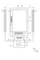
- FIG. 1 is a plan view illustrating a detection device according to a first embodiment.
- FIG. 2 is a block diagram showing an example of the configuration of the detection device according to the first embodiment.
- FIG. 3 is a circuit diagram showing the detection device according to the first embodiment.
- FIG. 4 is an enlarged schematic diagram of the sensor unit.
- FIG. 5 is a cross-sectional view taken along line V-V' of FIG.
- FIG. 6 is a plan view showing a schematic arrangement of the lower electrode and the insulating film.
- FIG. 7 is a cross-sectional view taken along line VII-VII' of FIG.
- FIG. 8 is a plan view showing a schematic arrangement of the lower electrode and the insulating film in the detection device according to the second embodiment.
- FIG. 9 is a cross-sectional view taken along line IX-IX' of FIG.
- FIG. 10 is a plan view showing a schematic arrangement of the lower electrode and the insulating film in the detection device according to the third embodiment.
- FIG. 11 is a cross-sectional view taken along line XI-XI' of FIG.
- FIG. 12 is a cross-sectional view illustrating a detection device according to a fourth embodiment.
- FIG. 13 is a cross-sectional view that illustrates a detection device according to a modified example of the fourth embodiment.
- the term "on top” is used, unless otherwise specified, to include both a case in which another structure is placed directly on top of a structure so as to be in contact with the structure, and a case in which another structure is placed above a structure via yet another structure.
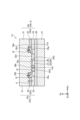
- First Embodiment Fig. 1 is a plan view showing a detection device according to the first embodiment.
- the detection device 1 has a sensor substrate 21 (substrate), a sensor unit 10, a gate line driving circuit 15, a signal line selection circuit 16, a detection circuit 48, a control circuit 122, a power supply circuit 123, a first light source substrate 51, a second light source substrate 52, and light sources 53 and 54.
- a plurality of light sources 53 are provided on the first light source substrate 51.
- a plurality of light sources 54 are provided on the second light source substrate 52.
- the control board 121 is electrically connected to the sensor substrate 21 via the wiring board 71.
- the wiring board 71 is, for example, a flexible printed circuit board or a rigid board.
- the detection circuit 48 is provided on the wiring board 71.
- the control board 121 is provided with a control circuit 122 and a power supply circuit 123.
- the control circuit 122 is, for example, an FPGA (Field Programmable Gate Array).
- the control circuit 122 supplies control signals to the sensor unit 10, the gate line driving circuit 15, and the signal line selection circuit 16 to control the detection operation of the sensor unit 10.
- the control circuit 122 also supplies control signals to the light sources 53 and 54 to control the lighting or non-lighting of the light sources 53 and 54.
- the power supply circuit 123 supplies voltage signals such as a sensor power supply signal VDDSNS (see FIG. 3) to the sensor unit 10, the gate line driving circuit 15, and the signal line selection circuit 16. In addition, the power supply circuit 123 supplies power supply voltage to the light sources 53 and 54.
- VDDSNS sensor power supply signal
- the sensor substrate 21 has a detection area AA and a peripheral area GA.
- the detection area AA is an area in which the multiple photodiodes PD (see FIG. 4) of the sensor unit 10 are provided.
- the peripheral area GA is an area between the outer periphery of the detection area AA and the outer edge of the sensor substrate 21, and is an area in which the multiple photodiodes PD are not provided.
- the gate line driving circuit 15 and the signal line selection circuit 16 are provided in the peripheral area GA. Specifically, the gate line driving circuit 15 is provided in a region of the peripheral area GA that extends along the second direction Dy. The signal line selection circuit 16 is provided in a region of the peripheral area GA that extends along the first direction Dx, and is provided between the sensor unit 10 and the detection circuit 48.
- the first direction Dx is a direction in a plane parallel to the sensor substrate 21.
- the second direction Dy is a direction in a plane parallel to the sensor substrate 21, and is a direction perpendicular to the first direction Dx.
- the second direction Dy may intersect the first direction Dx without being perpendicular to it.
- the third direction Dz is a direction perpendicular to the first direction Dx and the second direction Dy, and is the normal direction of the main surface of the sensor substrate 21.
- plane view refers to the positional relationship when viewed from a direction perpendicular to the sensor substrate 21.
- the multiple light sources 53 are provided on the first light source substrate 51 and are arranged along the second direction Dy.
- the multiple light sources 54 are provided on the second light source substrate 52 and are arranged along the second direction Dy.
- the first light source substrate 51 and the second light source substrate 52 are electrically connected to the control circuit 122 and the power supply circuit 123 via terminal portions 124 and 125, respectively, provided on the control board 121.
- the multiple light sources 53 and the multiple light sources 54 may be, for example, inorganic light-emitting diodes (LEDs) or organic light-emitting diodes (OLEDs).
- the multiple light sources 53 and the multiple light sources 54 each emit light of a different wavelength.
- the first light emitted from the light source 53 is mainly reflected by the surface of the object to be detected, such as a finger, and enters the sensor unit 10. This allows the sensor unit 10 to detect a fingerprint by detecting the uneven shape of the surface of the finger.
- the second light emitted from the light source 54 is mainly reflected inside the finger or passes through the finger and enters the sensor unit 10. This allows the sensor unit 10 to detect information about a living body inside the finger.
- Information about a living body includes, for example, the pulse waves, pulse, and blood vessel images of the finger or palm.
- the detection device 1 may be configured as a fingerprint detection device that detects fingerprints, or a vein detection device that detects blood vessel patterns such as veins.
- the detection device 1 is provided with multiple types of light sources 53, 54 as light sources. However, this is not limited to this, and there may be only one type of light source. For example, multiple light sources 53 and multiple light sources 54 may be arranged on each of the first light source substrate 51 and the second light source substrate 52. Furthermore, there may be one or three or more light source substrates on which the light sources 53 and the light sources 54 are arranged. Alternatively, it is sufficient that at least one or more light sources are arranged.
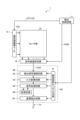
- FIG. 2 is a block diagram showing an example of the configuration of the detection device according to the first embodiment.
- the detection device 1 further includes a detection control circuit 11 and a detection unit 40. Some or all of the functions of the detection control circuit 11 are included in the control circuit 122. In addition, some or all of the functions of the detection unit 40 other than the detection circuit 48 are included in the control circuit 122.
- the sensor unit 10 has multiple photodiodes PD.
- the photodiodes PD of the sensor unit 10 output an electrical signal corresponding to the irradiated light as a detection signal Vdet to the signal line selection circuit 16.
- the sensor unit 10 also performs detection according to the gate drive signal VGL supplied from the gate line drive circuit 15.
- the detection control circuit 11 is a circuit that supplies control signals to the gate line drive circuit 15, the signal line selection circuit 16, and the detection unit 40, respectively, and controls their operation.
- the detection control circuit 11 supplies various control signals, such as a start signal STV and a clock signal CK, to the gate line drive circuit 15.
- the detection control circuit 11 also supplies various control signals, such as a selection signal ASW, to the signal line selection circuit 16.
- the detection control circuit 11 also supplies various control signals to the light sources 53 and 54, controlling their lighting and non-lighting.
- the gate line driving circuit 15 is a circuit that drives multiple gate lines GL (see FIG. 3) based on various control signals.
- the gate line driving circuit 15 selects multiple gate lines GL sequentially or simultaneously, and supplies a gate driving signal VGL to the selected gate lines GL. In this way, the gate line driving circuit 15 selects multiple photodiodes PD connected to the gate lines GL.
- the signal line selection circuit 16 is a switch circuit that sequentially or simultaneously selects multiple signal lines SL (see FIG. 3).
- the signal line selection circuit 16 is, for example, a multiplexer.
- the signal line selection circuit 16 connects the selected signal line SL to the detection circuit 48 based on the selection signal ASW supplied from the detection control circuit 11. As a result, the signal line selection circuit 16 outputs the detection signal Vdet of the photodiode PD to the detection unit 40.
- the detection unit 40 includes a detection circuit 48, a signal processing circuit 44, a coordinate extraction circuit 45, a memory circuit 46, and a detection timing control circuit 47.
- the detection timing control circuit 47 controls the detection circuit 48, the signal processing circuit 44, and the coordinate extraction circuit 45 to operate in synchronization based on a control signal supplied from the detection control circuit 11.
- the detection circuit 48 is, for example, an analog front-end circuit (AFE).
- the detection circuit 48 is a signal processing circuit having at least the functions of a detection signal amplifier circuit 42 and an A/D conversion circuit 43.
- the detection signal amplifier circuit 42 amplifies the detection signal Vdet.
- the A/D conversion circuit 43 converts the analog signal output from the detection signal amplifier circuit 42 into a digital signal.
- the signal processing circuit 44 is a logic circuit that detects a predetermined physical quantity input to the sensor unit 10 based on the output signal of the detection circuit 48. When a finger is in contact with or close to the detection surface, the signal processing circuit 44 can detect unevenness on the surface of the finger or palm based on the signal from the detection circuit 48. The signal processing circuit 44 can also detect information about the living body based on the signal from the detection circuit 48. Information about the living body includes, for example, blood vessel images of the finger or palm, pulse waves, pulse rate, blood oxygen concentration, etc.
- the memory circuit 46 temporarily stores the signal calculated by the signal processing circuit 44.
- the memory circuit 46 may be, for example, a RAM (Random Access Memory), a register circuit, etc.
- the coordinate extraction circuit 45 is a logic circuit that determines the detection coordinates of the unevenness of the surface of a finger, etc., when the signal processing circuit 44 detects contact or proximity of a finger.
- the coordinate extraction circuit 45 is also a logic circuit that determines the detection coordinates of the blood vessels of the finger or palm.
- the coordinate extraction circuit 45 combines the detection signals Vdet output from each photodiode PD of the sensor unit 10 to generate two-dimensional information indicating the shape of the unevenness of the surface of the finger, etc., and two-dimensional information indicating the shape of the blood vessels of the finger or palm.
- the coordinate extraction circuit 45 may output the detection signal Vdet as the sensor output voltage Vo without calculating the detection coordinates.
- FIG. 3 is a circuit diagram showing the detection device according to the first embodiment. Note that FIG. 3 also shows the circuit configuration of the detection circuit 48.
- the sensor pixel PX includes a photodiode PD, a capacitance element Ca, and a drive transistor Tr.
- the capacitance element Ca is a capacitance (sensor capacitance) formed in the photodiode PD, and is equivalently connected in parallel with the photodiode PD.
- FIG. 3 of the multiple gate lines GL, two gate lines GL(m) and GL(m+1) aligned in the second direction Dy are shown. Also, of the multiple signal lines SL, two signal lines SL(n) and SL(n+1) aligned in the first direction Dx are shown.
- the sensor pixel PX is the area surrounded by the gate line GL and the signal line SL.
- the drive transistor Tr is provided corresponding to each of the multiple photodiodes PD.
- the drive transistor Tr is composed of a thin film transistor, and in this example, is composed of an n-channel MOS (Metal Oxide Semiconductor) type TFT (Thin Film Transistor).
- Each of the multiple gate lines GL is connected to the gates of multiple drive transistors Tr arranged in a first direction Dx.
- Each of the multiple signal lines SL is connected to one of the sources and drains of multiple drive transistors Tr arranged in a second direction Dy.
- the other of the sources and drains of the multiple drive transistors Tr is connected to the anode of the photodiode PD and the capacitance element Ca.
- the cathode of the photodiode PD is supplied with a sensor power supply signal VDDSNS from the power supply circuit 123 (see FIG. 1).
- the signal line SL and the capacitance element Ca are supplied with a sensor reference voltage COM, which is the initial potential of the signal line SL and the capacitance element Ca, from the power supply circuit 123 via the reset transistor TrR.
- the switch SSW of the detection circuit 48 is turned on and connected to the signal line SL.
- the detection signal amplifier circuit 42 of the detection circuit 48 converts the fluctuation in the current supplied from the signal line SL into a fluctuation in voltage and amplifies it.
- a reference potential (Vref) having a fixed potential is input to the non-inverting input section (+) of the detection signal amplifier circuit 42, and the signal line SL is connected to the inverting input section (-).
- a signal equal to the sensor reference voltage COM is input as the reference potential (Vref) voltage.
- the control circuit 122 see FIG.
- the detection signal amplifier circuit 42 also has a capacitance element Cb and a reset switch RSW. During the reset period, the reset switch RSW is turned on and the charge of the capacitance element Cb is reset.
- the driving transistor Tr is not limited to an n-type TFT, and may be a p-type TFT.
- the pixel circuit of the sensor pixel PX shown in FIG. 3 is merely an example, and the sensor pixel PX may be provided with multiple transistors corresponding to one photodiode PD.
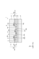
- FIG. 4 is an enlarged schematic diagram of the sensor unit.
- the detection device 1 has a plurality of photodiodes PD provided on a sensor substrate 21, and an insulating film 35.
- the plurality of gate lines GL each extend in a first direction Dx and are arranged at intervals in a second direction Dy.
- the plurality of signal lines SL each extend in a second direction Dy and are arranged at intervals in the first direction Dx.
- the plurality of photodiodes PD are provided in an area surrounded by two gate lines GL and two signal lines SL, and are arranged in a matrix on the sensor substrate 21.
- the lower electrodes 23 of the photodiodes PD are arranged in a matrix on the sensor substrate 21 in correspondence with each of the multiple photodiodes PD.
- the right and bottom edges of the lower electrodes 23 are arranged to overlap with parts of the signal line SL and gate line GL, respectively.
- the left and top edges of the lower electrodes 23 are arranged at intervals from the signal line SL and gate line GL, respectively. This makes it possible to increase the area of the lower electrodes 23 in the region surrounded by the two gate lines GL and the two signal lines SL, thereby improving the detection sensitivity of the photodiodes PD.
- the drive transistor Tr is provided in a region overlapping with the lower electrode 23 of the photodiode PD.
- the drive transistor Tr has a semiconductor layer 61, a source electrode 62, a drain electrode 63, and a gate electrode 64.
- the semiconductor layer 61 extends along the gate line GL and is provided so as to intersect with the gate electrode 64 in a planar view.
- the gate electrode 64 is connected to the gate line GL and extends in a direction (second direction Dy) perpendicular to the gate line GL.
- One end of the semiconductor layer 61 is connected to a source electrode 62 via contact hole CH2.
- the source electrode 62 is connected to a connection wiring 65 and a connection pad 66, and is drawn out to the center of the photodiode PD (lower electrode 23).
- the lower electrode 23 is connected to the connection pad 66 at its center via contact hole CH1.
- the source electrode 62 of the drive transistor Tr is electrically connected to the photodiode PD.
- the other end of the semiconductor layer 61 is connected to a drain electrode 63 via contact hole CH3.
- the drain electrode 63 is connected to the signal line SL.
- the insulating film 35 is provided between adjacent lower electrodes 23 in the first direction Dx and the second direction Dy, and is provided to cover the peripheral portion of the lower electrode 23. More specifically, the insulating film 35 is formed in a lattice shape with a first extension portion 35a and a second extension portion 35b intersecting. The first extension portion 35a extends in the second direction Dy. The first extension portion 35a is provided to overlap the signal line SL and extends along the signal line SL. The second extension portion 35b extends in the first direction Dx. The second extension portion 35b is provided to overlap the gate line GL and is provided along the gate line GL.
- an opening OP is formed in the insulating film 35 in an area overlapping each of the multiple lower electrodes 23.
- the opening OP is an area surrounded by two first extension portions 35a and two second extension portions 35b.
- the island portion 35c is provided at a distance from the first extension portion 35a and the second extension portion 35b, and is provided in an area overlapping the contact hole CH1 in the center of the photodiode PD (lower electrode 23).
- the shapes, arrangement pitch, etc. of the lower electrode 23 and insulating film 35 shown in FIG. 4 are merely examples, and can be changed as appropriate depending on the characteristics and detection accuracy required for the detection device 1.
- FIG. 5 is a cross-sectional view taken along line V-V' in FIG. 4.
- the detection device 1 has a circuit formation layer 29, an insulating film 27, a photodiode PD, and a sealing film 90 laminated in this order on a sensor substrate 21.
- the sensor substrate 21 is an insulating substrate, and may be, for example, a glass substrate such as quartz or non-alkali glass.
- the sensor substrate 21 is not limited to being flat, and may have a curved surface. In this case, the sensor substrate 21 may be a film-like resin material.
- the circuit formation layer 29 is provided on the sensor substrate 21, and is a layer on which various transistors such as the drive transistor Tr shown in Figures 3 and 4, and various wiring such as the gate line GL and signal line SL are formed.
- Figure 5 shows the signal line SL connected to the drive transistor Tr.
- the insulating film 27 is provided on the circuit formation layer 29 including the drive transistor Tr, covering the signal line SL.
- the insulating film 27 is an organic planarizing film formed from an organic insulating material.
- the insulating film 28 is provided on the insulating film 27.
- the insulating film 28 is a barrier film made of an inorganic insulating material such as silicon nitride (SiN).
- the photodiode PD and insulating film 35 are provided on the insulating film 28. More specifically, the photodiode PD has a lower electrode 23, a lower buffer layer 32, an active layer 31, an upper buffer layer 33, and an upper electrode 24.
- the photodiode PD is stacked in the order of the lower electrode 23, the lower buffer layer 32 (hole transport layer), the active layer 31, the upper buffer layer 33 (electron transport layer), and the upper electrode 24 in a direction perpendicular to the sensor substrate 21.
- the photodiode PD of this embodiment is an OPD (Organic Photodiode) in which an organic semiconductor is used as the active layer 31.
- the lower electrode 23 is an anode electrode of the photodiode PD, and is formed of a conductive material having light transmission, such as ITO (Indium Tin Oxide).
- the lower electrode 23 is provided separately for each photodiode PD.
- the lower buffer layer 32, active layer 31, upper buffer layer 33, and upper electrode 24 are provided continuously across multiple photodiodes PD. Specifically, the lower buffer layer 32, active layer 31, upper buffer layer 33, and upper electrode 24 are provided overlapping the lower electrode 23 of the adjacent photodiode PD-1 and the lower electrode 23 of the photodiode PD-2, and are also provided overlapping the insulating film 35 between the photodiodes PD-1 and PD-2.
- the insulating film 35 (first extension portion 35a) is provided on the insulating film 28 between adjacent lower electrodes 23, and covers the peripheral portion of the lower electrode 23.
- the insulating film 35 is formed of an inorganic insulating material such as a silicon nitride film (SiN) or a silicon oxide film (SiO 2 ).
- the insulating film 35 (first extension portion 35a) insulates the lower electrodes 23 of adjacent photodiodes PD.
- the detailed configuration of the insulating film 35 will be described later with reference to FIGS. 6 and 7.
- the contact hole CH1 is provided in the center of the lower electrode 23, penetrating the insulating film 27 in the thickness direction (third direction Dz).
- the lower electrode 23 is connected to the connection pad 66 at the bottom of the contact hole CH1.
- the island-shaped portion 35c is provided to cover the contact hole CH1, and covers the lower electrode 23 inside the contact hole CH1.
- the island-shaped portion 35c overlaps the connection pad 66 in a plan view.
- the characteristics (for example, voltage-current characteristics and resistance value) of the active layer 31 change depending on the light irradiated.
- An organic material is used as the material of the active layer 31.
- the active layer 31 is a bulk heterostructure in which a p-type organic semiconductor and an n-type fullerene derivative (PCBM), which is an n-type organic semiconductor, are mixed.
- PCBM n-type fullerene derivative
- low molecular weight organic materials such as C60 (fullerene), PCBM (phenyl C61-butyric acid methyl ester), CuPc (copper phthalocyanine), F16CuPc (fluorinated copper phthalocyanine), rubrene (5,6,11,12-tetraphenyltetracene), and PDI (perylene derivative) can be used as the active layer 31.
- C60 fulllerene
- PCBM phenyl C61-butyric acid methyl ester
- CuPc copper phthalocyanine
- F16CuPc fluorinated copper phthalocyanine
- rubrene 5,6,11,12-tetraphenyltetracene
- PDI perylene derivative
- the active layer 31 can be formed by a deposition type (dry process) using these low molecular weight organic materials.
- the active layer 31 may be, for example, a laminated film of CuPc and F16CuPc, or a laminated film of rubrene and C60.
- the active layer 31 can also be formed by a coating type (wet process).
- the active layer 31 is made of a material that combines the above-mentioned low molecular weight organic material and a polymer organic material.
- the polymer organic material for example, P3HT (poly(3-hexylthiophene)), F8BT (F8-alt-benzothiadiazole), etc. can be used.
- the active layer 31 can be a film in which P3HT and PCBM are mixed, or a film in which F8BT and PDI are mixed.
- the lower buffer layer 32 is a hole transport layer
- the upper buffer layer 33 is an electron transport layer.
- the lower buffer layer 32 and the upper buffer layer 33 are provided to facilitate the arrival of holes and electrons generated in the active layer 31 to the lower electrode 23 or the upper electrode 24.
- the lower buffer layer 32 (hole transport layer) is directly in contact with the upper surface of the lower electrode 23, and is also provided on the insulating film 35 between adjacent lower electrodes 23.
- the active layer 31 is directly in contact with the upper surface of the lower buffer layer 32.
- the material of the hole transport layer is a metal oxide layer. As the metal oxide layer, tungsten oxide (WO 3 ), molybdenum oxide, or the like is used.
- the upper buffer layer 33 (electron transport layer) is in direct contact with the active layer 31, and the upper electrode 24 is in direct contact with the upper buffer layer 33.
- the material used for the electron transport layer is ethoxylated polyethyleneimine (PEIE).
- the materials and manufacturing methods of the lower buffer layer 32, active layer 31, and upper buffer layer 33 are merely examples, and other materials and manufacturing methods may be used.
- the lower buffer layer 32 and upper buffer layer 33 are not limited to single-layer films, and may be formed as a laminated film including an electron blocking layer and a hole blocking layer.
- the upper electrode 24 is provided on the upper buffer layer 33.
- the upper electrode 24 is the cathode electrode of the photodiode PD, and is formed continuously over the entire detection area AA. In other words, the upper electrode 24 is provided continuously over the multiple photodiodes PD.
- the upper electrode 24 faces the multiple lower electrodes 23, sandwiching the lower buffer layer 32, the active layer 31, and the upper buffer layer 33 between them.
- the upper electrode 24 is formed of a conductive material having translucency, such as ITO or IZO.
- the upper electrode 24 may be a laminated film of multiple conductive materials having translucency.
- the sealing film 90 is provided on the upper electrode 24.
- an inorganic film such as a silicon nitride film or an aluminum oxide film, or a resin film such as acrylic is used.
- the sealing film 90 is not limited to a single layer, and may be a laminated film of two or more layers combining the inorganic film and the resin film.
- the sealing film 90 provides a good seal for the photodiode PD, and can prevent moisture from entering from the upper surface side.
- the configuration of the photodiode PD shown in Figures 4 and 5 is merely an example and can be modified as appropriate.
- the upper electrode 24 may be the anode electrode of the photodiode PD
- the lower electrode 23 may be the cathode electrode of the photodiode PD.
- FIG. 6 is a plan view showing a schematic arrangement of the lower electrode and the insulating film.
- FIG. 7 is a cross-sectional view taken along line VII-VII' in FIG. 6. In FIG. 6, the insulating film 35 is shown hatched to make the drawing easier to see.
- FIG. 7 is also a cross-sectional view showing an enlarged view of area A shown by the dashed line in FIG. 5.
- the insulating film 35 is provided in a lattice pattern covering the peripheral portion of the lower electrode 23.
- the first extension portion 35a is provided between adjacent lower electrodes 23 in the first direction Dx and extends in the second direction Dy along the sides of the lower electrodes 23.
- the second extension portion 35b is provided between adjacent lower electrodes 23 in the second direction Dy and extends in the first direction Dx along the sides of the lower electrodes 23.
- the insulating film 35 (first extension portion 35a and second extension portion 35b) has multiple grooves 35G extending between adjacent lower electrodes 23 and along the sides of the lower electrodes 23.
- the grooves 35G are located between adjacent lower electrodes 23 and surround the lower electrodes 23 in a plan view.
- two grooves 35G are provided between adjacent lower electrodes 23.
- the two grooves 35G extend along the respective extension directions of the first extension portion 35a and the second extension portion 35b, and are provided adjacent to each other in the respective width directions of the first extension portion 35a and the second extension portion 35b.
- the insulating film 35 (first extension portion 35a and second extension portion 35b) is separated into three parts by the two grooves 35G.
- the insulating film 35 has electrode side overlapping portions 35e, 35g separated by two grooves 35G, and a protrusion 35f.
- the electrode side overlapping portion 35e is provided overlapping the side of the lower electrode 23 of the photodiode PD-1, and extends along the side of the lower electrode 23 (the right side in FIG. 6).
- the electrode side overlapping portion 35g is provided overlapping the side of the lower electrode 23 of the photodiode PD-2 (the left side in FIG. 6), and extends along the side of the lower electrode 23.
- the protrusion 35f is located between the two grooves 35G, and extends along the electrode side overlapping portions 35e, 35g.
- the electrode edge overlapping portions 35e and 35g overlap the four sides of the lower electrode 23, and are formed in a frame shape surrounding the lower electrode 23.
- the protruding portion 35f is provided in a position between the lower electrodes 23 that does not overlap with the lower electrode 23.
- the protruding portion 35f is provided in a lattice shape so as to surround each of the lower electrodes 23 arranged in a matrix.
- the width of the convex portion 35f is smaller than the width of the groove portions 35G (width in the first direction Dx) and is smaller than the distance between adjacent lower electrodes 23.
- the thickness of the insulating film 35 (electrode edge overlapping portions 35e, 35g and convex portion 35f) provided between adjacent lower electrodes 23 is, for example, 20 nm or more and 200 nm or less.
- the film thickness of the lower electrode 23 is, for example, 20 nm or more and 100 nm or less.
- the lower buffer layer 32 covers at least a portion of the lower electrode 23 of the photodiode PD-1, the lower electrode 23 of the photodiode PD-2, and the insulating film 35 adjacent in the first direction Dx, and is also provided inside the two grooves 35G. More specifically, the lower buffer layer 32 includes an electrode overlapping portion 32a that overlaps the lower electrode 23, insulating film overlapping portions 32b, 32c, and 32d that overlap at least a portion of the insulating film 35, and a groove overlapping portion 32e that is provided on the insulating film 28 inside the groove 35G.
- the electrode overlapping portion 32a is provided in an area of the lower electrode 23 where the insulating film 35 is not provided (opening OP (see FIG. 4)).
- the insulating film overlapping portion 32b is provided on the electrode side overlapping portion 35e of the insulating film 35.
- the insulating film overlapping portion 32c is provided on the convex portion 35f of the insulating film 35.
- the insulating film overlapping portion 32d is provided on the electrode side overlapping portion 35g of the insulating film 35.
- the lower buffer layer 32 is formed by, for example, a coating method to cover the lower electrode 23 and the insulating film 35.
- the lower buffer layer 32 tends to accumulate in the recess formed by the groove 35G, the protrusion 35f, and the electrode side overlapping portions 35e, 35g, and also tends to accumulate in the recess formed by the lower electrode 23 and the electrode side overlapping portions 35e, 35g of the insulating film 35 (i.e., the region overlapping with the opening OP (see FIG. 4)).
- the lower buffer layer 32 applied on the insulating film 35 is formed thinly by flowing from above the insulating film 35 toward the groove 35G side or the lower electrode 23 side.
- the thicknesses t2, t3, and t4 of the insulating film overlapping portions 32b, 32c, and 32d of the lower buffer layer 32 are thinner than the thickness t1 of the electrode overlapping portion 32a of the lower buffer layer 32.
- the thicknesses t2, t3, and t4 of the insulating film overlapping portions 32b, 32c, and 32d of the lower buffer layer 32 are thinner than the thickness t5 of the groove overlapping portion 32e of the lower buffer layer 32.
- the insulating film overlapping portions 32b, 32c, and 32d of the lower buffer layer 32 located between adjacent lower electrodes 23 have a higher resistance value than the electrode overlapping portion 32a. Therefore, the lower buffer layer 32 (insulating film overlapping portions 32b, 32c, and 32d) in the region overlapping with the insulating film 35 functions as a potential barrier between adjacent lower electrodes 23. Therefore, in this embodiment, the leakage current flowing between adjacent lower electrodes 23 can be suppressed compared to when the lower buffer layer 32 is provided continuously with a constant thickness across multiple adjacent photodiodes PD.
- the lower buffer layer 32 provided on the insulating film 35 is disconnected at the step formed by the groove 35G and the protrusion 35f. Specifically, the lower buffer layer 32 (insulating film overlapping portion 32c) provided on the protrusion 35f of the insulating film 35 is provided at a distance from the lower buffer layer 32 (groove overlapping portion 32e) provided in the groove 35G.
- the lower buffer layer 32 (insulating film overlapping portions 32b, 32d) provided on the electrode side overlapping portion 35e of the insulating film 35 is provided at a distance from the lower buffer layer 32 (groove overlapping portion 32e) provided in the groove 35G.
- the width (width in the first direction Dx) of the protrusion 35f of the insulating film 35 is formed smaller than the width (width in the first direction Dx) of the multiple grooves 35G, so that a good disconnection can be generated between the insulating film overlapping portion 32c and the groove overlapping portion 32e.
- adjacent photodiodes PD e.g., photodiodes PD-1 and PD-2
- a separated and discontinuous portion is formed between the lower buffer layer 32 provided in the photodiode PD-1 and the lower buffer layer 32 provided in the photodiode PD-2. This enables the detection device 1 to effectively suppress leakage current flowing between adjacent lower electrodes 23.
- the insulating film 35 forms the insulating film overlapping portions 32b, 32c, and 32d of the lower buffer layer 32 as high resistance regions, so the spacing between the lower electrodes 23 (or the width of the insulating film 35) can be made smaller than when the electrode overlapping portion 32a of the lower buffer layer 32 and the insulating film overlapping portions 32b, 32c, and 32d are formed with a constant thickness. This makes it possible to increase the area of the effective detection area AA of the detection device 1 and improve the detection sensitivity. Alternatively, the area of the lower electrode 23 can be reduced, allowing the detection device 1 to have a high resolution.
- the spacing between the lower electrodes 23 (or the width of the insulating film 35) can be made small, which makes it possible to suppress delays in the arrival time of carriers (holes and electrons) generated in the active layer 31 between the portion of the photodiode PD that overlaps with the insulating film 35 and the portion of the photodiode PD that does not overlap with the insulating film 35.
- the insulating film 35 has two grooves 35G between the adjacent lower electrodes 23, but is not limited to this.
- One or three or more grooves 35G may be provided between the adjacent lower electrodes 23.
- the insulating film 35 may not have the grooves 35G.
- at least the thicknesses t2 and t4 of the insulating film overlapping parts 32b and 32d of the lower buffer layer 32 are formed thinner than the thickness t1 of the electrode overlapping part 32a of the lower buffer layer 32. Therefore, even if the insulating film 35 does not have the grooves 35G, the detection device 1 can suppress the leakage current flowing between the adjacent lower electrodes 23.
- the electrode side overlapping portions 35e and 35g of the insulating film 35 are provided continuously, surrounding each of the lower electrodes 23.
- the protruding portion 35f of the insulating film 35 is provided continuously across multiple lower electrodes 23.
- the lower buffer layer 32 is provided overlapping each of the electrode side overlapping portions 35e, 35g and the convex portion 35f of the insulating film 35.
- the lower buffer layer 32 does not have to be provided on a part of the insulating film 35.
- Fig. 8 is a plan view showing a schematic arrangement of the lower electrode and the insulating film in the detection device according to the second embodiment.
- Fig. 9 is a cross-sectional view taken along the line IX-IX' in Fig. 8.
- the insulating film 35 and the wall portion 26 are shown hatched to make the drawing easier to see.
- the same components as those described in the above embodiment are designated by the same reference numerals, and duplicated description will be omitted.
- the insulating film 35 does not have a groove portion 35G, and is provided continuously between adjacent lower electrodes 23.
- the detection device 1A also has a wall portion 26 provided between adjacent lower electrodes 23 and spaced apart from the multiple lower electrodes 23.
- the wall portion 26 extends along the sides of the lower electrodes 23 and is provided surrounding the lower electrodes 23 in a planar view.
- the wall portion 26 is also provided overlapping the insulating film 35 and extends along the extension direction of the insulating film 35. In the example shown in FIG. 8, two wall portions 26 are provided between adjacent lower electrodes 23.
- the two wall portions 26 are provided on the insulating film 28 in the same layer as the multiple lower electrodes 23, and are made of the same material as the multiple lower electrodes 23.
- the two wall portions 26 are made of a translucent conductive material such as ITO.
- the thickness of each wall portion 26 is, for example, 20 nm or more and 100 nm or less.
- the insulating film 35 is provided between the adjacent lower electrodes 23, covering the two wall portions 26.
- the insulating film 35 is provided along the unevenness formed by the lower electrodes 23 and the two wall portions 26, and is formed with multiple unevenness. Specifically, in the photodiode PD-1 and photodiode PD-2 adjacent in the first direction Dx, the insulating film 35 has electrode edge overlapping portions 35e, 35g and two convex portions 35h.
- the electrode edge overlapping portion 35e is provided overlapping the side (the right side in FIG. 8) of the lower electrode 23 of the photodiode PD-1, and extends along the side of the lower electrode 23.
- the electrode edge overlapping portion 35g is provided overlapping the side (the left side in FIG. 8) of the lower electrode 23 of the photodiode PD-2, and extends along the side of the lower electrode 23.
- the protrusions 35h are provided overlapping the two wall portions 26, and extend along the electrode edge overlapping portions 35e, 35g.
- the lower buffer layer 32 is provided to cover at least a portion of the lower electrode 23 of the photodiode PD-1, the lower electrode 23 of the photodiode PD-2, and the insulating film 35 that are adjacent in the first direction Dx. More specifically, the lower buffer layer 32 includes an electrode overlapping portion 32a that overlaps the lower electrode 23, insulating film overlapping portions 32b and 32d that overlap the electrode edge overlapping portions 35e and 35g of the insulating film 35, respectively, and a recess overlapping portion 32f that is provided inside the recess 35i.
- the lower buffer layer 32 is not provided on the two protruding portions 35h. However, similar to the insulating film overlapping portion 32c shown in FIG. 7, the lower buffer layer 32 may be provided on the two protruding portions 35h.
- the thicknesses t2 and t4 of the insulating film overlapping portions 32b and 32d of the lower buffer layer 32 are also thinner than the thickness t1 of the electrode overlapping portion 32a of the lower buffer layer 32. Furthermore, the thicknesses t2 and t4 of the insulating film overlapping portions 32b and 32d of the lower buffer layer 32 are also thinner than the thickness t5 of the recess overlapping portion 32f of the lower buffer layer 32.
- the concave portion overlapping portion 32f provided on each of the two concave portions 35i is provided separated by the convex portion 35h.
- the lower buffer layer 32 provided on the convex portion 35h and the concave portion overlapping portion 32f of the concave portion 35i are provided separated from each other. In other words, the lower buffer layer 32 is stepped by the convex portion 35h and the concave portion 35i.
- the insulating film overlapping portions 32b and 32d of the lower buffer layer 32 located between adjacent lower electrodes 23 have a higher resistance value than the electrode overlapping portion 32a.
- the lower buffer layer 32 provided on the insulating film 35 is disconnected at the steps formed by the convex portions 35h and the concave portions 35i, etc. As a result, even in this embodiment, it is possible to suppress the leakage current flowing between adjacent lower electrodes 23.
- Fig. 10 is a plan view showing a schematic arrangement of a lower electrode and an insulating film in a detection device according to a third embodiment
- Fig. 11 is a cross-sectional view taken along the line XI-XI' of Fig. 10.
- the detection device 1B has an organic insulating film 36 instead of the insulating film 35 made of an inorganic insulating material.
- the organic insulating film 36 may be made of the same organic insulating material as the insulating film 27, for example.
- the organic insulating film 36 is provided between the lower electrodes 23 adjacent to each other in the first direction Dx and the second direction Dy, and is provided to cover the peripheral portions of the lower electrodes 23.
- the organic insulating film 36 is formed in a lattice pattern with first extension portions 36a and second extension portions 36b intersecting.
- the first extension portions 36a are provided between adjacent lower electrodes 23 in the first direction Dx, and extend in the second direction Dy along the sides of the lower electrodes 23.
- the second extension portions 36b are provided between adjacent lower electrodes 23 in the second direction Dy, and extend in the first direction Dx along the sides of the lower electrodes 23.
- the organic insulating film 36 also includes an island-shaped portion 36c that is spaced apart from the first extension portion 36a and the second extension portion 36b.
- the island-shaped portion 36c is provided in a region that overlaps with the contact hole CH1 (see FIG. 5) at the center of the photodiode PD (lower electrode 23).
- the island-shaped portion 36c is not limited to an organic insulating film, and may be formed of an inorganic insulating film.
- the height (thickness) of the organic insulating film 36 is greater than the height (film thickness) of the insulating film 35 formed from the inorganic insulating material described above.
- the lower buffer layers 32 of the adjacent photodiodes PD-1 and PD-2 are separated from each other by the organic insulating film 36. More specifically, the outer edge 32g of the lower buffer layer 32 of the photodiode PD-1 is disposed so as to overlap the inclined surface of the organic insulating film 36.
- the outer edge 32h of the lower buffer layer 32 of the photodiode PD-2 is disposed so as to overlap the inclined surface of the organic insulating film 36 on the side opposite to the outer edge 32g.
- the lower buffer layer 32 is not provided at least on the top of the organic insulating film 36. In other words, the lower buffer layer 32 is provided within the region surrounded by the first extension 36a and the second extension 36b of the organic insulating film 36.
- the lower buffer layer 32 is provided at a distance for each of the multiple photodiodes PD (lower electrodes 23) by the organic insulating film 36.
- the leakage current flowing between adjacent lower electrodes 23 can be suppressed compared to when the lower buffer layer 32 is provided continuously across multiple adjacent photodiodes PD.
- FIG. 12 is a cross-sectional view that shows a schematic diagram of a detection device according to the fourth embodiment.
- the insulating film 35 is a laminated film in which a first insulating film 37 and a second insulating film 38 are laminated.
- the second insulating film 38 is laminated on the first insulating film 37.
- the first insulating film 37 is formed of, for example, a silicon oxide film
- the second insulating film 38 is formed of a material different from the first insulating film 37, for example, a silicon nitride film.
- a groove portion 35G is formed in the insulating film 35, penetrating the first insulating film 37 and the second insulating film 38 in the thickness direction (third direction Dz).
- the configuration of the insulating film 35 and the groove portion 35G in a plan view is the same as that of the first embodiment described above (see FIG. 6), and a repeated description will be omitted.
- the ends of the insulating film 35 each have an inverted tapered shape. More specifically, the end 38a of the second insulating film 38 is provided to protrude in the first direction Dx further than the end 37a of the first insulating film 37. The end 38a of the second insulating film 38 is provided in an eave-like shape relative to the end 37a of the first insulating film 37.
- the inner walls of the groove 35G also have an inverse tapered shape.
- the end 38b of the second insulating film 38 protrudes further than the end 37b of the first insulating film 37.
- the distance between the inner walls of the second insulating film 38 that face each other in the first direction Dx is smaller than the distance between the inner walls of the first insulating film 37 that face each other in the first direction Dx.
- the inverted tapered shape of the insulating film 35 can be formed by utilizing the difference in etching rate between the first insulating film 37 and the second insulating film 38 when patterning the first insulating film 37 and the second insulating film 38 by photolithography and etching.
- the etching rate of the first insulating film 37 is greater than the etching rate of the second insulating film 38.
- a space is formed at the end of the insulating film 35 (electrode side overlapping portions 35e, 35g) surrounded by the end 38a of the second insulating film 38 that protrudes like an eave, the end 37a of the first insulating film 37, and the lower electrode 23.
- the electrode overlapping portion 32a of the lower buffer layer 32 is also provided inside the space surrounded by the end 37a of the first insulating film 37, the end 38a of the second insulating film 38, and the lower electrode 23. This makes it easier for a step to occur between the electrode overlapping portion 32a of the lower buffer layer 32 and the insulating film overlapping portion 32b.
- a space is formed that is surrounded by the end portion 38b of the second insulating film 38, the end portion 37b of the first insulating film 37, and the insulating film 28.
- the groove portion overlapping portion 32e of the lower buffer layer 32 is also provided inside the space surrounded by the end portion 38b of the second insulating film 38, the end portion 37b of the first insulating film 37, and the insulating film 28.
- the groove 35G is formed in a straight shape, and the space of the groove 35G is larger than in a configuration that is not formed in an inverted tapered shape (see FIG. 7).
- the groove overlapping portion 32e of the lower buffer layer 32 and the insulating film overlapping portion 32b are more likely to be disconnected.
- the thicknesses t2 and t4 of the insulating film overlapping portions 32b and 32d of the lower buffer layer 32 are thinner than the thickness t1 of the electrode overlapping portion 32a of the lower buffer layer 32.
- the thicknesses t2 and t4 of the insulating film overlapping portions 32b and 32d of the lower buffer layer 32 are thinner than the thickness t5 of the groove overlapping portion 32e of the lower buffer layer 32.
- the lower buffer layer 32 is not provided on the second insulating film 38 of the convex portion 35f.
- the lower buffer layer 32 may be provided on the second insulating film 38 of the convex portion 35f.
- the groove portion 35G is formed in an inverted tapered shape, the lower buffer layer 32 provided on the convex portion 35f and the groove overlapping portion 32e of the groove portion 35G are provided at a distance. In other words, the lower buffer layer 32 is stepped at the convex portion 35f and the groove portion 35G.
- FIG. 13 is a cross-sectional view showing a schematic configuration of a detection device according to a modification of the fourth embodiment. As shown in Fig. 13, the detection device 1D according to the modification of the fourth embodiment is different from the detection device 1C according to the fourth embodiment (see Fig. 12) in that the groove portion 35G is not provided.
- the insulating film 35 (first insulating film 37 and second insulating film 38) is provided continuously between adjacent lower electrodes 23.
- the ends of the insulating film 35 are each formed in an inverse tapered shape. More specifically, the end 38a of the second insulating film 38 is formed in an inverse tapered shape, protruding further in the first direction Dx than the end 37a of the first insulating film 37.
- the electrode overlapping portion 32a of the lower buffer layer 32 and the insulating film overlapping portions 32b, 32d are easily separated and are provided at a distance.
- the thicknesses t2, t4 of the insulating film overlapping portions 32b, 32d of the lower buffer layer 32 are thinner than the thickness t1 of the electrode overlapping portion 32a of the lower buffer layer 32. Therefore, even in a configuration in which the groove portion 35G is not provided in this modified example, the leakage current flowing between adjacent lower electrodes 23 can be suppressed.
Landscapes
- Solid State Image Pick-Up Elements (AREA)
Priority Applications (2)
| Application Number | Priority Date | Filing Date | Title |
|---|---|---|---|
| JP2024552970A JPWO2024090261A1 (https=) | 2022-10-26 | 2023-10-16 | |
| US19/188,582 US20250255085A1 (en) | 2022-10-26 | 2025-04-24 | Detection device |
Applications Claiming Priority (2)
| Application Number | Priority Date | Filing Date | Title |
|---|---|---|---|
| JP2022-171667 | 2022-10-26 | ||
| JP2022171667 | 2022-10-26 |
Related Child Applications (1)
| Application Number | Title | Priority Date | Filing Date |
|---|---|---|---|
| US19/188,582 Continuation US20250255085A1 (en) | 2022-10-26 | 2025-04-24 | Detection device |
Publications (1)
| Publication Number | Publication Date |
|---|---|
| WO2024090261A1 true WO2024090261A1 (ja) | 2024-05-02 |
Family
ID=90830643
Family Applications (1)
| Application Number | Title | Priority Date | Filing Date |
|---|---|---|---|
| PCT/JP2023/037349 Ceased WO2024090261A1 (ja) | 2022-10-26 | 2023-10-16 | 検出装置 |
Country Status (3)
| Country | Link |
|---|---|
| US (1) | US20250255085A1 (https=) |
| JP (1) | JPWO2024090261A1 (https=) |
| WO (1) | WO2024090261A1 (https=) |
Citations (3)
| Publication number | Priority date | Publication date | Assignee | Title |
|---|---|---|---|---|
| JP2010153834A (ja) * | 2008-11-28 | 2010-07-08 | Semiconductor Energy Lab Co Ltd | フォトセンサ及び表示装置 |
| WO2021153470A1 (ja) * | 2020-01-31 | 2021-08-05 | ソニーグループ株式会社 | 光電変換素子および撮像素子 |
| JP2022160898A (ja) * | 2021-04-07 | 2022-10-20 | 株式会社ジャパンディスプレイ | 検出装置及び撮像装置 |
-
2023
- 2023-10-16 JP JP2024552970A patent/JPWO2024090261A1/ja active Pending
- 2023-10-16 WO PCT/JP2023/037349 patent/WO2024090261A1/ja not_active Ceased
-
2025
- 2025-04-24 US US19/188,582 patent/US20250255085A1/en active Pending
Patent Citations (3)
| Publication number | Priority date | Publication date | Assignee | Title |
|---|---|---|---|---|
| JP2010153834A (ja) * | 2008-11-28 | 2010-07-08 | Semiconductor Energy Lab Co Ltd | フォトセンサ及び表示装置 |
| WO2021153470A1 (ja) * | 2020-01-31 | 2021-08-05 | ソニーグループ株式会社 | 光電変換素子および撮像素子 |
| JP2022160898A (ja) * | 2021-04-07 | 2022-10-20 | 株式会社ジャパンディスプレイ | 検出装置及び撮像装置 |
Also Published As
| Publication number | Publication date |
|---|---|
| US20250255085A1 (en) | 2025-08-07 |
| JPWO2024090261A1 (https=) | 2024-05-02 |
Similar Documents
| Publication | Publication Date | Title |
|---|---|---|
| JP7633109B2 (ja) | 検出装置 | |
| JP7751416B2 (ja) | 検出装置 | |
| JP7806217B2 (ja) | 検出装置 | |
| JP7818127B2 (ja) | 検出装置 | |
| JP2026020189A (ja) | 電子機器 | |
| JP7811642B2 (ja) | 検出装置 | |
| US12364091B2 (en) | Detection device | |
| JP7806101B2 (ja) | 検出装置 | |
| JP7684887B2 (ja) | 検出装置 | |
| JP7606941B2 (ja) | 検出装置 | |
| WO2024090261A1 (ja) | 検出装置 | |
| JP7362385B2 (ja) | 検出装置 | |
| JP7745081B2 (ja) | 検出装置 | |
| WO2024135561A1 (ja) | 検出装置 | |
| WO2024135768A1 (ja) | 検出装置 | |
| WO2026048984A1 (ja) | 検出装置 | |
| WO2026042483A1 (ja) | 検出装置及び検出装置の製造方法 | |
| WO2024257502A1 (ja) | 検出装置 | |
| WO2026053915A1 (ja) | 検出装置及び検出装置の製造方法 | |
| WO2025105160A1 (ja) | 検出装置 | |
| WO2026034159A1 (ja) | 検出装置及び検出装置の製造方法 | |
| US20240196634A1 (en) | Detection device and method for manufacturing same | |
| JP2026028505A (ja) | 検出装置及び検出装置の製造方法 | |
| WO2024262191A1 (ja) | 検出装置及び検出装置の製造方法 | |
| JP2025148873A (ja) | 電子機器 |
Legal Events
| Date | Code | Title | Description |
|---|---|---|---|
| 121 | Ep: the epo has been informed by wipo that ep was designated in this application |
Ref document number: 23882467 Country of ref document: EP Kind code of ref document: A1 |
|
| WWE | Wipo information: entry into national phase |
Ref document number: 2024552970 Country of ref document: JP |
|
| NENP | Non-entry into the national phase |
Ref country code: DE |
|
| 122 | Ep: pct application non-entry in european phase |
Ref document number: 23882467 Country of ref document: EP Kind code of ref document: A1 |