WO2024090261A1 - Dispositif de détection - Google Patents
Dispositif de détection Download PDFInfo
- Publication number
- WO2024090261A1 WO2024090261A1 PCT/JP2023/037349 JP2023037349W WO2024090261A1 WO 2024090261 A1 WO2024090261 A1 WO 2024090261A1 JP 2023037349 W JP2023037349 W JP 2023037349W WO 2024090261 A1 WO2024090261 A1 WO 2024090261A1
- Authority
- WO
- WIPO (PCT)
- Prior art keywords
- insulating film
- buffer layer
- detection device
- electrode
- lower electrodes
- Prior art date
Links
- 238000001514 detection method Methods 0.000 title claims abstract description 112
- 239000000758 substrate Substances 0.000 claims abstract description 38
- 239000000463 material Substances 0.000 claims description 11
- 229910052581 Si3N4 Inorganic materials 0.000 claims description 7
- 239000011810 insulating material Substances 0.000 claims description 7
- HQVNEWCFYHHQES-UHFFFAOYSA-N silicon nitride Chemical compound N12[Si]34N5[Si]62N3[Si]51N64 HQVNEWCFYHHQES-UHFFFAOYSA-N 0.000 claims description 7
- VYPSYNLAJGMNEJ-UHFFFAOYSA-N Silicium dioxide Chemical compound O=[Si]=O VYPSYNLAJGMNEJ-UHFFFAOYSA-N 0.000 claims description 4
- 229910052814 silicon oxide Inorganic materials 0.000 claims description 3
- 239000010408 film Substances 0.000 description 208
- 239000010410 layer Substances 0.000 description 151
- 230000002093 peripheral effect Effects 0.000 description 10
- 239000004065 semiconductor Substances 0.000 description 9
- 230000004048 modification Effects 0.000 description 8
- 238000012986 modification Methods 0.000 description 8
- 238000010586 diagram Methods 0.000 description 7
- 230000005525 hole transport Effects 0.000 description 7
- 238000000605 extraction Methods 0.000 description 6
- 239000011368 organic material Substances 0.000 description 6
- 238000007789 sealing Methods 0.000 description 6
- 210000004204 blood vessel Anatomy 0.000 description 5
- 239000004020 conductor Substances 0.000 description 4
- 238000005530 etching Methods 0.000 description 4
- 230000006870 function Effects 0.000 description 4
- 230000015572 biosynthetic process Effects 0.000 description 3
- 239000011159 matrix material Substances 0.000 description 3
- 229910044991 metal oxide Inorganic materials 0.000 description 3
- 150000004706 metal oxides Chemical class 0.000 description 3
- 229920000301 poly(3-hexylthiophene-2,5-diyl) polymer Polymers 0.000 description 3
- 239000011347 resin Substances 0.000 description 3
- 229920005989 resin Polymers 0.000 description 3
- YYMBJDOZVAITBP-UHFFFAOYSA-N rubrene Chemical compound C1=CC=CC=C1C(C1=C(C=2C=CC=CC=2)C2=CC=CC=C2C(C=2C=CC=CC=2)=C11)=C(C=CC=C2)C2=C1C1=CC=CC=C1 YYMBJDOZVAITBP-UHFFFAOYSA-N 0.000 description 3
- 210000003462 vein Anatomy 0.000 description 3
- XMWRBQBLMFGWIX-UHFFFAOYSA-N C60 fullerene Chemical class C12=C3C(C4=C56)=C7C8=C5C5=C9C%10=C6C6=C4C1=C1C4=C6C6=C%10C%10=C9C9=C%11C5=C8C5=C8C7=C3C3=C7C2=C1C1=C2C4=C6C4=C%10C6=C9C9=C%11C5=C5C8=C3C3=C7C1=C1C2=C4C6=C2C9=C5C3=C12 XMWRBQBLMFGWIX-UHFFFAOYSA-N 0.000 description 2
- 229920002873 Polyethylenimine Polymers 0.000 description 2
- 230000000903 blocking effect Effects 0.000 description 2
- 238000006243 chemical reaction Methods 0.000 description 2
- 238000000576 coating method Methods 0.000 description 2
- XCJYREBRNVKWGJ-UHFFFAOYSA-N copper(II) phthalocyanine Chemical compound [Cu+2].C12=CC=CC=C2C(N=C2[N-]C(C3=CC=CC=C32)=N2)=NC1=NC([C]1C=CC=CC1=1)=NC=1N=C1[C]3C=CC=CC3=C2[N-]1 XCJYREBRNVKWGJ-UHFFFAOYSA-N 0.000 description 2
- 239000011521 glass Substances 0.000 description 2
- 238000004519 manufacturing process Methods 0.000 description 2
- 230000003287 optical effect Effects 0.000 description 2
- 230000000149 penetrating effect Effects 0.000 description 2
- 229920000642 polymer Polymers 0.000 description 2
- 230000035945 sensitivity Effects 0.000 description 2
- 239000002356 single layer Substances 0.000 description 2
- 239000010409 thin film Substances 0.000 description 2
- 239000005964 Acibenzolar-S-methyl Substances 0.000 description 1
- -1 F16CuPc (fluorinated copper phthalocyanine Chemical class 0.000 description 1
- 229910004298 SiO 2 Inorganic materials 0.000 description 1
- NIXOWILDQLNWCW-UHFFFAOYSA-N acrylic acid group Chemical group C(C=C)(=O)O NIXOWILDQLNWCW-UHFFFAOYSA-N 0.000 description 1
- 239000003513 alkali Substances 0.000 description 1
- QVGXLLKOCUKJST-UHFFFAOYSA-N atomic oxygen Chemical compound [O] QVGXLLKOCUKJST-UHFFFAOYSA-N 0.000 description 1
- 230000004888 barrier function Effects 0.000 description 1
- 230000005540 biological transmission Effects 0.000 description 1
- 239000008280 blood Substances 0.000 description 1
- 210000004369 blood Anatomy 0.000 description 1
- 239000000969 carrier Substances 0.000 description 1
- 230000008859 change Effects 0.000 description 1
- 239000011248 coating agent Substances 0.000 description 1
- 230000001934 delay Effects 0.000 description 1
- 230000008021 deposition Effects 0.000 description 1
- 238000001035 drying Methods 0.000 description 1
- FJAOBQORBYMRNO-UHFFFAOYSA-N f16cupc Chemical compound [Cu+2].[N-]1C(N=C2C3=C(F)C(F)=C(F)C(F)=C3C(N=C3C4=C(F)C(F)=C(F)C(F)=C4C(=N4)[N-]3)=N2)=C(C(F)=C(F)C(F)=C2F)C2=C1N=C1C2=C(F)C(F)=C(F)C(F)=C2C4=N1 FJAOBQORBYMRNO-UHFFFAOYSA-N 0.000 description 1
- 229910003472 fullerene Inorganic materials 0.000 description 1
- RBTKNAXYKSUFRK-UHFFFAOYSA-N heliogen blue Chemical compound [Cu].[N-]1C2=C(C=CC=C3)C3=C1N=C([N-]1)C3=CC=CC=C3C1=NC([N-]1)=C(C=CC=C3)C3=C1N=C([N-]1)C3=CC=CC=C3C1=N2 RBTKNAXYKSUFRK-UHFFFAOYSA-N 0.000 description 1
- AMGQUBHHOARCQH-UHFFFAOYSA-N indium;oxotin Chemical compound [In].[Sn]=O AMGQUBHHOARCQH-UHFFFAOYSA-N 0.000 description 1
- 238000000034 method Methods 0.000 description 1
- 229910000476 molybdenum oxide Inorganic materials 0.000 description 1
- TWNQGVIAIRXVLR-UHFFFAOYSA-N oxo(oxoalumanyloxy)alumane Chemical compound O=[Al]O[Al]=O TWNQGVIAIRXVLR-UHFFFAOYSA-N 0.000 description 1
- PQQKPALAQIIWST-UHFFFAOYSA-N oxomolybdenum Chemical compound [Mo]=O PQQKPALAQIIWST-UHFFFAOYSA-N 0.000 description 1
- 229910052760 oxygen Inorganic materials 0.000 description 1
- 239000001301 oxygen Substances 0.000 description 1
- 238000000059 patterning Methods 0.000 description 1
- 125000002080 perylenyl group Chemical class C1(=CC=C2C=CC=C3C4=CC=CC5=CC=CC(C1=C23)=C45)* 0.000 description 1
- CSHWQDPOILHKBI-UHFFFAOYSA-N peryrene Natural products C1=CC(C2=CC=CC=3C2=C2C=CC=3)=C3C2=CC=CC3=C1 CSHWQDPOILHKBI-UHFFFAOYSA-N 0.000 description 1
- 125000001997 phenyl group Chemical group [H]C1=C([H])C([H])=C(*)C([H])=C1[H] 0.000 description 1
- 238000000206 photolithography Methods 0.000 description 1
- 238000005036 potential barrier Methods 0.000 description 1
- 230000008569 process Effects 0.000 description 1
- 239000010453 quartz Substances 0.000 description 1
- 238000006467 substitution reaction Methods 0.000 description 1
- ZNOKGRXACCSDPY-UHFFFAOYSA-N tungsten trioxide Chemical compound O=[W](=O)=O ZNOKGRXACCSDPY-UHFFFAOYSA-N 0.000 description 1
Images


Abstract
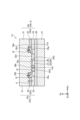
Ce dispositif de détection comprend : un substrat ; une pluralité de photodiodes dans lesquelles une électrode inférieure, une couche tampon inférieure, une couche active, une couche tampon supérieure et une électrode supérieure sont empilées dans l'ordre sur le substrat ; et un film isolant qui est disposé entre la pluralité d'électrodes inférieures adjacentes. La couche tampon inférieure comprend une partie de chevauchement d'électrode qui chevauche l'électrode inférieure et une partie de chevauchement de film isolant qui chevauche au moins une partie du film isolant, l'épaisseur de la partie de chevauchement de film isolant de la couche tampon inférieure étant inférieure à l'épaisseur de la partie de chevauchement d'électrode de la couche tampon inférieure.
Applications Claiming Priority (2)
| Application Number | Priority Date | Filing Date | Title |
|---|---|---|---|
| JP2022-171667 | 2022-10-26 | ||
| JP2022171667 | 2022-10-26 |
Publications (1)
| Publication Number | Publication Date |
|---|---|
| WO2024090261A1 true WO2024090261A1 (fr) | 2024-05-02 |
Family
ID=90830643
Family Applications (1)
| Application Number | Title | Priority Date | Filing Date |
|---|---|---|---|
| PCT/JP2023/037349 WO2024090261A1 (fr) | 2022-10-26 | 2023-10-16 | Dispositif de détection |
Country Status (1)
| Country | Link |
|---|---|
| WO (1) | WO2024090261A1 (fr) |
Citations (3)
| Publication number | Priority date | Publication date | Assignee | Title |
|---|---|---|---|---|
| JP2010153834A (ja) * | 2008-11-28 | 2010-07-08 | Semiconductor Energy Lab Co Ltd | フォトセンサ及び表示装置 |
| WO2021153470A1 (fr) * | 2020-01-31 | 2021-08-05 | ソニーグループ株式会社 | Élément de conversion photoélectrique et élément d'imagerie |
| JP2022160898A (ja) * | 2021-04-07 | 2022-10-20 | 株式会社ジャパンディスプレイ | 検出装置及び撮像装置 |
-
2023
- 2023-10-16 WO PCT/JP2023/037349 patent/WO2024090261A1/fr unknown
Patent Citations (3)
| Publication number | Priority date | Publication date | Assignee | Title |
|---|---|---|---|---|
| JP2010153834A (ja) * | 2008-11-28 | 2010-07-08 | Semiconductor Energy Lab Co Ltd | フォトセンサ及び表示装置 |
| WO2021153470A1 (fr) * | 2020-01-31 | 2021-08-05 | ソニーグループ株式会社 | Élément de conversion photoélectrique et élément d'imagerie |
| JP2022160898A (ja) * | 2021-04-07 | 2022-10-20 | 株式会社ジャパンディスプレイ | 検出装置及び撮像装置 |
Similar Documents
| Publication | Publication Date | Title |
|---|---|---|
| US11888080B2 (en) | Detection device including light sources along an outer circumference of two detection areas each of the detection areas having a specific scan direction | |
| KR101981318B1 (ko) | 발광 지문 인식 패널 및 이를 포함하는 지문 인식 디스플레이 장치 | |
| US11943943B2 (en) | Detection device | |
| WO2022024781A1 (fr) | Dispositif de détection | |
| CN113711362B (zh) | 包括薄膜晶体管和有机光电二极管的图像传感器阵列器件 | |
| WO2024090261A1 (fr) | Dispositif de détection | |
| JP7362385B2 (ja) | 検出装置 | |
| US20220328564A1 (en) | Detection device and imaging device | |
| WO2021049262A1 (fr) | Dispositif de détection | |
| WO2023223877A1 (fr) | Dispositif de détection | |
| WO2023153262A1 (fr) | Dispositif de détection | |
| WO2023182032A1 (fr) | Dispositif de détection | |
| US20230028839A1 (en) | Detection device | |
| WO2023149195A1 (fr) | Dispositif de détection | |
| US20230105043A1 (en) | Electronic device | |
| WO2023171431A1 (fr) | Dispositif de détection | |
| JP2023012379A (ja) | 検出装置 | |
| JP2023030472A (ja) | 検出装置 | |
| JP2023030471A (ja) | 検出装置 | |
| JP2022190538A (ja) | 検出装置 | |
| JP2023068878A (ja) | 検出装置 | |
| WO2023032863A1 (fr) | Dispositif de détection | |
| US20240049487A1 (en) | Optical sensor | |
| WO2022220287A1 (fr) | Dispositif de détection | |
| WO2022176503A1 (fr) | Dispositif de détection |