WO2024090178A1 - 蒸発源、成膜装置、及び成膜方法 - Google Patents
蒸発源、成膜装置、及び成膜方法 Download PDFInfo
- Publication number
- WO2024090178A1 WO2024090178A1 PCT/JP2023/036492 JP2023036492W WO2024090178A1 WO 2024090178 A1 WO2024090178 A1 WO 2024090178A1 JP 2023036492 W JP2023036492 W JP 2023036492W WO 2024090178 A1 WO2024090178 A1 WO 2024090178A1
- Authority
- WO
- WIPO (PCT)
- Prior art keywords
- evaporation source
- film forming
- film
- chamber
- substrate
- Prior art date
- Legal status (The legal status is an assumption and is not a legal conclusion. Google has not performed a legal analysis and makes no representation as to the accuracy of the status listed.)
- Ceased
Links
Images
Classifications
-
- C—CHEMISTRY; METALLURGY
- C23—COATING METALLIC MATERIAL; COATING MATERIAL WITH METALLIC MATERIAL; CHEMICAL SURFACE TREATMENT; DIFFUSION TREATMENT OF METALLIC MATERIAL; COATING BY VACUUM EVAPORATION, BY SPUTTERING, BY ION IMPLANTATION OR BY CHEMICAL VAPOUR DEPOSITION, IN GENERAL; INHIBITING CORROSION OF METALLIC MATERIAL OR INCRUSTATION IN GENERAL
- C23C—COATING METALLIC MATERIAL; COATING MATERIAL WITH METALLIC MATERIAL; SURFACE TREATMENT OF METALLIC MATERIAL BY DIFFUSION INTO THE SURFACE, BY CHEMICAL CONVERSION OR SUBSTITUTION; COATING BY VACUUM EVAPORATION, BY SPUTTERING, BY ION IMPLANTATION OR BY CHEMICAL VAPOUR DEPOSITION, IN GENERAL
- C23C14/00—Coating by vacuum evaporation, by sputtering or by ion implantation of the coating forming material
- C23C14/22—Coating by vacuum evaporation, by sputtering or by ion implantation of the coating forming material characterised by the process of coating
- C23C14/24—Vacuum evaporation
- C23C14/243—Crucibles for source material
-
- C—CHEMISTRY; METALLURGY
- C23—COATING METALLIC MATERIAL; COATING MATERIAL WITH METALLIC MATERIAL; CHEMICAL SURFACE TREATMENT; DIFFUSION TREATMENT OF METALLIC MATERIAL; COATING BY VACUUM EVAPORATION, BY SPUTTERING, BY ION IMPLANTATION OR BY CHEMICAL VAPOUR DEPOSITION, IN GENERAL; INHIBITING CORROSION OF METALLIC MATERIAL OR INCRUSTATION IN GENERAL
- C23C—COATING METALLIC MATERIAL; COATING MATERIAL WITH METALLIC MATERIAL; SURFACE TREATMENT OF METALLIC MATERIAL BY DIFFUSION INTO THE SURFACE, BY CHEMICAL CONVERSION OR SUBSTITUTION; COATING BY VACUUM EVAPORATION, BY SPUTTERING, BY ION IMPLANTATION OR BY CHEMICAL VAPOUR DEPOSITION, IN GENERAL
- C23C14/00—Coating by vacuum evaporation, by sputtering or by ion implantation of the coating forming material
- C23C14/06—Coating by vacuum evaporation, by sputtering or by ion implantation of the coating forming material characterised by the coating material
- C23C14/12—Organic material
-
- C—CHEMISTRY; METALLURGY
- C23—COATING METALLIC MATERIAL; COATING MATERIAL WITH METALLIC MATERIAL; CHEMICAL SURFACE TREATMENT; DIFFUSION TREATMENT OF METALLIC MATERIAL; COATING BY VACUUM EVAPORATION, BY SPUTTERING, BY ION IMPLANTATION OR BY CHEMICAL VAPOUR DEPOSITION, IN GENERAL; INHIBITING CORROSION OF METALLIC MATERIAL OR INCRUSTATION IN GENERAL
- C23C—COATING METALLIC MATERIAL; COATING MATERIAL WITH METALLIC MATERIAL; SURFACE TREATMENT OF METALLIC MATERIAL BY DIFFUSION INTO THE SURFACE, BY CHEMICAL CONVERSION OR SUBSTITUTION; COATING BY VACUUM EVAPORATION, BY SPUTTERING, BY ION IMPLANTATION OR BY CHEMICAL VAPOUR DEPOSITION, IN GENERAL
- C23C14/00—Coating by vacuum evaporation, by sputtering or by ion implantation of the coating forming material
- C23C14/22—Coating by vacuum evaporation, by sputtering or by ion implantation of the coating forming material characterised by the process of coating
- C23C14/225—Oblique incidence of vaporised material on substrate
-
- C—CHEMISTRY; METALLURGY
- C23—COATING METALLIC MATERIAL; COATING MATERIAL WITH METALLIC MATERIAL; CHEMICAL SURFACE TREATMENT; DIFFUSION TREATMENT OF METALLIC MATERIAL; COATING BY VACUUM EVAPORATION, BY SPUTTERING, BY ION IMPLANTATION OR BY CHEMICAL VAPOUR DEPOSITION, IN GENERAL; INHIBITING CORROSION OF METALLIC MATERIAL OR INCRUSTATION IN GENERAL
- C23C—COATING METALLIC MATERIAL; COATING MATERIAL WITH METALLIC MATERIAL; SURFACE TREATMENT OF METALLIC MATERIAL BY DIFFUSION INTO THE SURFACE, BY CHEMICAL CONVERSION OR SUBSTITUTION; COATING BY VACUUM EVAPORATION, BY SPUTTERING, BY ION IMPLANTATION OR BY CHEMICAL VAPOUR DEPOSITION, IN GENERAL
- C23C14/00—Coating by vacuum evaporation, by sputtering or by ion implantation of the coating forming material
- C23C14/22—Coating by vacuum evaporation, by sputtering or by ion implantation of the coating forming material characterised by the process of coating
- C23C14/228—Gas flow assisted PVD deposition
-
- C—CHEMISTRY; METALLURGY
- C23—COATING METALLIC MATERIAL; COATING MATERIAL WITH METALLIC MATERIAL; CHEMICAL SURFACE TREATMENT; DIFFUSION TREATMENT OF METALLIC MATERIAL; COATING BY VACUUM EVAPORATION, BY SPUTTERING, BY ION IMPLANTATION OR BY CHEMICAL VAPOUR DEPOSITION, IN GENERAL; INHIBITING CORROSION OF METALLIC MATERIAL OR INCRUSTATION IN GENERAL
- C23C—COATING METALLIC MATERIAL; COATING MATERIAL WITH METALLIC MATERIAL; SURFACE TREATMENT OF METALLIC MATERIAL BY DIFFUSION INTO THE SURFACE, BY CHEMICAL CONVERSION OR SUBSTITUTION; COATING BY VACUUM EVAPORATION, BY SPUTTERING, BY ION IMPLANTATION OR BY CHEMICAL VAPOUR DEPOSITION, IN GENERAL
- C23C14/00—Coating by vacuum evaporation, by sputtering or by ion implantation of the coating forming material
- C23C14/22—Coating by vacuum evaporation, by sputtering or by ion implantation of the coating forming material characterised by the process of coating
- C23C14/24—Vacuum evaporation
- C23C14/26—Vacuum evaporation by resistance or inductive heating of the source
-
- H—ELECTRICITY
- H10—SEMICONDUCTOR DEVICES; ELECTRIC SOLID-STATE DEVICES NOT OTHERWISE PROVIDED FOR
- H10K—ORGANIC ELECTRIC SOLID-STATE DEVICES
- H10K50/00—Organic light-emitting devices
- H10K50/10—OLEDs or polymer light-emitting diodes [PLED]
-
- H—ELECTRICITY
- H10—SEMICONDUCTOR DEVICES; ELECTRIC SOLID-STATE DEVICES NOT OTHERWISE PROVIDED FOR
- H10K—ORGANIC ELECTRIC SOLID-STATE DEVICES
- H10K71/00—Manufacture or treatment specially adapted for the organic devices covered by this subclass
- H10K71/10—Deposition of organic active material
- H10K71/16—Deposition of organic active material using physical vapour deposition [PVD], e.g. vacuum deposition or sputtering
- H10K71/164—Deposition of organic active material using physical vapour deposition [PVD], e.g. vacuum deposition or sputtering using vacuum deposition
Definitions
- the present invention relates to an evaporation source, a film forming apparatus, and a film forming method.
- Patent Document 1 discloses a technique in which a protruding reflector is provided on multiple evaporation source nozzles and positioned on a portion of the outside of the multiple evaporation source nozzles to suppress a drop in temperature of the multiple nozzles.
- Patent Document 1 cannot sufficiently suppress the drop in nozzle temperature, and the drop in nozzle temperature makes it easier for material to accumulate in the nozzle, which can result in variation in film formation characteristics.
- the object of the present invention is to provide an evaporation source, a film formation device, and a film formation method that can suppress variation in film formation characteristics.
- the present invention employs the following measures to solve the above problems.
- the evaporation source of the present invention is An evaporation source that forms a film while moving relative to a substrate, a nozzle for ejecting a film forming material that is evaporated or sublimated by heating the film forming material contained in a material container; A cylindrical member disposed so as to surround an outer periphery of the nozzle;
- the present invention is characterized by comprising:
- the present invention makes it possible to suppress variation in film formation characteristics.
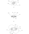
- FIG. 1 is a schematic configuration diagram of a film forming apparatus according to an embodiment of the present invention.
- 1 is a schematic configuration diagram of a film forming apparatus according to an embodiment of the present invention.
- FIG. 2 is a schematic cross-sectional view of an evaporation source according to an embodiment of the present invention.
- FIG. 2 is a schematic cross-sectional view of an evaporation source according to an embodiment of the present invention.
- 11A and 11B are explanatory diagrams of a modified example of an evaporation source according to an embodiment of the present invention.
- 1A to 1C are explanatory diagrams of a method for manufacturing an electronic device.
- the direction of movement of the evaporation source is defined as the first direction X
- the direction intersecting the first direction X is defined as the second direction Y. More specifically, in each embodiment, the second direction Y is a direction perpendicular to the first direction X and parallel to the film formation surface of the substrate on which the film is formed.
- Example 2 An evaporation source according to an embodiment of the present invention, a film forming apparatus including the evaporation source, and a film forming method using the evaporation source will be described with reference to FIGS.
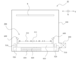
- FIG. 1 is a schematic diagram of the film forming apparatus according to the embodiment of the present invention, and shows a simplified configuration as seen from the front side.
- Figure 2 is a schematic diagram of the film forming apparatus according to the embodiment of the present invention, and shows a simplified configuration as seen from above. Note that Figures 1 and 2 show the main components in a see-through manner.
- the film formation apparatus 10 in this embodiment is an evaporation apparatus that performs vacuum deposition.
- the film formation apparatus 10 includes a chamber 100, a vacuum pump 200 for creating a vacuum (reduced pressure atmosphere) inside the chamber 100, and an evaporation source 300 disposed inside the chamber 100.
- the evaporation source 300 serves to evaporate or sublimate the film formation material M to be evaporated onto the substrate S disposed inside the chamber 100 by heating the material.
- the material evaporated or sublimated by the evaporation source 300 adheres to the substrate S, forming a thin film on the substrate S.
- the film forming apparatus 10 also includes an atmospheric box 410 for supplying electricity and cooling liquid to the evaporation source 300, and a first atmospheric arm 420 and a second atmospheric arm 430 that move in accordance with the movement of the atmospheric box 410.
- the atmospheric box 410 is hollow inside and is configured to communicate with the outside of the chamber 100 through the insides of the first atmospheric arm 420 and the second atmospheric arm 430. Therefore, the inside of the atmospheric box 410 is exposed to the atmosphere.
- wiring connected to a power source provided outside the chamber 100 and a cooling pipe connected to a cooling liquid supply device provided outside the chamber 100 can be connected to the evaporation source 300.
- the first atmospheric arm 420 and the second atmospheric arm 430 are provided to arrange wiring and cooling pipes within the cavity of the moving atmospheric box 410. That is, the first atmospheric arm 420 and the second atmospheric arm 430 are configured to have a hollow interior and to move in accordance with the movement of the atmospheric box 410. More specifically, one end of the second atmospheric arm 430 is configured to be rotatable relative to the bottom plate of the chamber 100. One end of the first atmospheric arm 420 is rotatably supported relative to the other end of the second atmospheric arm 430, and the other end is rotatably supported relative to the atmospheric box 410.
- the film forming apparatus 10 is also provided with a moving mechanism for moving the evaporation source 300.
- the moving mechanism includes a pair of guide rails 520, a pair of gears 510 provided on both sides of a rotation shaft that passes through the atmospheric box 410, and a drive source (not shown) such as a motor that rotates the rotation shaft.
- the pair of guide rails 520 are provided with racks that mesh with the pair of gears 510, respectively.
- the evaporation source 300 is configured to be guided by a pair of guide rails 520, and configured to move linearly back and forth in the first direction X. Then, by evaporating or sublimating the film-forming material M while moving the evaporation source 300 in the first direction X, a thin film can be formed on the substrate S. Note that film formation can be performed during at least one of the forward and return movements of the evaporation source 300. In this manner, film formation is performed while the evaporation source 300 moves relative to the substrate S.
- the movement mechanism in this embodiment employs a so-called rack and pinion mechanism.
- the movement mechanism for reciprocating the atmospheric box 410 and the evaporation source 300 is not limited to a rack and pinion mechanism, and various known technologies such as a ball screw mechanism may be employed.
- a film thickness monitor 600 is provided on each side of the evaporation source 300 in the second direction Y for measuring the film thickness of the film formed on the substrate S.
- the film thickness monitor 600 measures the film thickness of the film formed on the substrate S by measuring the film thickness of the film formed on the film thickness monitor 600 and predicting the film thickness of the film formed on the substrate S based on the film thickness.
- the amount of film formation e.g., controlling the amount of heat applied to the film forming material M in the evaporation source 300
- the thickness of the thin film formed on the substrate S can be adjusted to the desired thickness.
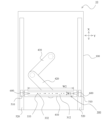
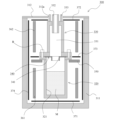
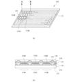
- FIG. 3 is a simplified cross-sectional view of the evaporation source 300 cut along a plane perpendicular to the second direction Y and passing through the nozzle center
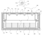
- Figure 4 is a simplified cross-sectional view of the evaporation source 300 cut along a plane perpendicular to the first direction X and passing through the nozzle center. Note that a large number of nozzles are provided ( Figures 1 and 2 show a case where 14 nozzles are provided), but for convenience, Figure 4 shows only four nozzles.
- the evaporation source 300 has a rectangular parallelepiped case.
- This case has a case body 311 with a bottom plate portion and four side plate portions, and a lid portion 312 that covers most of the upper opening of the case body 311.
- the case body 311 has a heat insulating function.
- a passage can be formed inside the case body 311, and a cooling liquid such as cooling water can be run through this passage to provide a heat insulating effect.
- the evaporation source 300 also includes a material container (crucible) provided in the case.
- This material container includes a lower crucible 320 forming a material chamber 321 and an upper crucible 330 forming a diffusion chamber 331.
- a plurality of nozzles 332 are provided on the upper surface of the upper crucible 330.
- the lower crucible 320 and the upper crucible 330 are fixed by a fixing device B such as a bolt with a middle plate 340 having an introduction pipe 341 for connecting the material chamber 321 and the diffusion chamber 331 sandwiched between them.
- the material chamber 321 is a chamber used to contain the film forming material M.
- the diffusion chamber 331 is a chamber for diffusing the material evaporated or sublimated by heating the film forming material contained in the material chamber 321 before it reaches the plurality of nozzles 332, adjusting the pressure distribution, and adjusting the inflow amount to the plurality of nozzles 332.
- the material evaporated or sublimated in the material chamber 321 is introduced into the diffusion chamber 331 by the inlet pipe 341, where it is diffused and ejected from the nozzles 332 into the chamber 100.
- the material container configured as described above is supported by the support member 350, and is fixed to the case while being positioned within the case.
- the evaporation source 300 also includes a first heater 361 for heating the lower crucible 320 and a second heater 362 for heating the upper crucible 330.
- the first heater 361 is provided between the outer wall surface of the lower crucible 320 and the inner wall surface of the case body 311, and the second heater 362 is provided between the outer wall surface of the upper crucible 330 and the inner wall surface of the case body 311.
- the first heater 361 and the second heater 362 are also provided on the front and back sides of the paper. That is, the first heater 361 and the second heater 362 are provided so as to surround the outer wall surfaces of the lower crucible 320 and the upper crucible 330, respectively.
- the first heater 361 and the second heater 362 a member that generates heat when electricity is applied, such as a sheath heater, can be suitably used.
- the first heater 361 heats the film forming material M contained in the lower crucible 320, causing it to evaporate or sublime.
- the second heater 362 prevents the evaporated or sublimated material from solidifying in the diffusion chamber 331 of the upper crucible 330.
- reflectors 371, 372, 373, and 374 are provided between the bottom surface of the case body 311 and the material container, between the lower surface of the lid portion 312 and the material container, between the first heater 361 and the second heater 362, and between the inner wall surface of the case body 311 and the material container. These reflectors 371, 372, 373, and 374 can prevent heat from the first heater 361 and the second heater 362 from being transmitted to the case, so that the material chamber 321 and the diffusion chamber 331 can be efficiently heated and heat can be prevented from escaping to the outside of the case. Note that by adopting a configuration in which multiple reflectors are arranged side by side between the case body 311 and various members, the heating efficiency can be further improved.
- a plurality of cylindrical members 333 are provided so as to surround the outer circumference of each of the plurality of nozzles 332.
- FIG. 4 a part of a plan view of the vicinity of the nozzle 332 seen from above is shown at the top of the cross-sectional view.
- the cylindrical member 333 has a cylindrical shape, but the shape is not limited as long as it is cylindrical.
- through holes 312a are provided at the positions where the plurality of nozzles 332 and the cylindrical members 333 are provided.
- the nozzles 332 and the cylindrical members 333 are configured to pass through the through holes 312a and have their tips protrude above the upper surface of the lid portion 312.
- a configuration can be adopted in which the reflector 372 arranged between the lower surface of the lid portion 312 and the material container is provided with a protrusion 372a that protrudes upward so as to face the outer wall surface of the cylindrical member 333.
- the protrusion 372a is arranged to surround the cylindrical member 333. More specifically, the shape of the protrusion 372a is cylindrical. However, the protrusion 372a only needs to exhibit a heat insulating function, and does not necessarily have to surround the cylindrical member 333. In the example shown in FIG. 5(a)(b), the protrusion 372a is configured to surround one cylindrical member 333.
- FIG. 5(c) shows a configuration in which one protrusion 372a surrounds two cylindrical members 333, but it is also possible to adopt a configuration in which one protrusion 372a surrounds three or more cylindrical members 333.
- Figure 6(a) is an overall view of the organic EL display device 150
- Figure 6(b) shows the cross-sectional structure of one pixel.
- each light-emitting element has a structure including an organic layer sandwiched between a pair of electrodes.
- the pixel referred to here refers to the smallest unit that allows a desired color to be displayed in the display area 151.
- the pixel 152 is configured by a combination of a first light-emitting element 152R, a second light-emitting element 152G, and a third light-emitting element 152B that emit light different from each other.
- the pixel 152 is often configured by a combination of a red light-emitting element, a green light-emitting element, and a blue light-emitting element, but may also be a combination of a yellow light-emitting element, a cyan light-emitting element, and a white light-emitting element, and is not particularly limited as long as it is at least one color.
- FIG. 6(b) is a schematic partial cross-sectional view taken along line A-B in FIG. 6(a).
- Pixel 152 is made up of a plurality of light-emitting elements, each of which has a first electrode (anode) 154, a hole transport layer 155, one of light-emitting layers 156R, 156G, or 156B, an electron transport layer 157, and a second electrode (cathode) 158 on a substrate 153.
- hole transport layer 155, light-emitting layers 156R, 156G, or 156B, and electron transport layer 157 are organic layers.
- light-emitting layer 156R is an organic EL layer that emits red light
- light-emitting layer 156G is an organic EL layer that emits green light
- light-emitting layer 156B is an organic EL layer that emits blue light.
- Light-emitting layers 156R, 156G, and 156B are formed in patterns that correspond to light-emitting elements (sometimes referred to as organic EL elements) that emit red, green, and blue light, respectively.
- the first electrode 154 is formed separately for each light-emitting element.
- the hole transport layer 155, the electron transport layer 157, and the second electrode 158 may be formed in common for the multiple light-emitting elements 152R, 152G, and 152B, or may be formed for each light-emitting element.
- an insulating layer 159 is provided between the first electrodes 154.
- a protective layer 140 is provided to protect the organic EL element from moisture and oxygen.
- the hole transport layer 155 and the electron transport layer 157 are shown as a single layer, but depending on the structure of the organic EL display element, they may be formed of multiple layers including a hole blocking layer and an electron blocking layer.
- a hole injection layer having an energy band structure that can smoothly inject holes from the first electrode 154 to the hole transport layer 155 can be formed between the first electrode 154 and the hole transport layer 155.
- an electron injection layer can be formed between the second electrode 158 and the electron transport layer 157.
- a circuit (not shown) for driving the organic EL display device and a substrate 153 on which a first electrode 154 are formed are prepared.
- Acrylic resin is formed by spin coating on the substrate 153 on which the first electrode 154 is formed, and the acrylic resin is patterned by lithography so that an opening is formed in the area where the first electrode 154 is formed, forming an insulating layer 159. This opening corresponds to the light-emitting area where the light-emitting element actually emits light.
- the substrate 153 with the patterned insulating layer 159 is carried into a first organic material deposition apparatus, and the substrate is held by a substrate support table and an electrostatic chuck, and a hole transport layer 155 is deposited as a common layer on the first electrode 154 in the display area.
- the hole transport layer 155 is deposited by vacuum deposition. In practice, the hole transport layer 155 is formed to be larger than the display area 151, so no high-resolution mask is required.
- the substrate 153 on which the hole transport layer 155 has been formed is carried into a second organic material deposition apparatus and held by a substrate support table and electrostatic chuck.
- the substrate and mask are aligned, the substrate is placed on the mask, and a red-emitting light-emitting layer 156R is deposited on the portion of the substrate 153 where the red-emitting element is to be located.
- Electron transport layer 157 is deposited over the entire display area 151 by a fifth deposition apparatus. Electron transport layer 157 is formed as a layer common to light-emitting layers 156R, 156G, and 156B of the three colors.
- the substrate on which the electron transport layer 157 has been formed is moved by a metallic deposition material deposition device to deposit the second electrode 158.
- the substrate is transferred to a plasma CVD device to deposit a protective layer 140, completing the organic EL display device 150.
- the substrate 153 on which the insulating layer 159 is patterned is exposed to an atmosphere containing moisture or oxygen from the time it is carried into the deposition apparatus until the deposition of the protective layer 140 is completed, the light-emitting layer made of the organic EL material may be deteriorated by moisture or oxygen. Therefore, in this embodiment, the substrate is carried in and out of the deposition apparatus in a vacuum atmosphere or an inert gas atmosphere.
- the evaporation source 300 includes a plurality of cylindrical members 333 arranged to surround the outer circumference of each of the nozzles 332. This makes it possible to suppress the temperature drop of the nozzles 332 and to suppress the variation in the film formation characteristics.
- the temperature drop at the tip of the nozzle 332 is suppressed, so that the deposition of material at the tip of the nozzle 332 can be suppressed.
- the temperature drop is suppressed even in the nozzles 332 near the end where the temperature is likely to drop, so that the variation in the temperature of each nozzle 332 can be suppressed. Therefore, even if it becomes necessary to increase the longitudinal length of the evaporation source 300 as the substrate S on which the film is formed becomes larger, the variation in the film formation characteristics can be suppressed.
- the size of the evaporation source 300 is about 850 mm in the X direction width W1 and about 2,600 mm in the Y direction width W2. Even with such a large-sized evaporation source 300, it is possible to suppress the temperature drop of the nozzle 332 near the end in the Y direction, and to suppress the variation in the film formation characteristics.
- the reflector 372 has a protruding portion 372a that protrudes upward so as to face the outer wall surface of the cylindrical member 333, it is possible to further suppress a decrease in the temperature of the nozzle 332.
- Figures 4 and 5 show a configuration in which the nozzles 332 extend straight in the vertical direction
- the direction in which the nozzles 332 extend is not limited.
- a configuration can be adopted in which the outermost nozzles 332 of the multiple nozzles 332 are inclined outward from the vertical direction.
- Film forming device 100 Chamber 200: Vacuum pump 300: Evaporation source 311: Case body 312: Lid 312a: Through hole 320: Lower crucible 321: Material chamber 330: Upper crucible 331: Diffusion chamber 332: Nozzle 333: Cylindrical member 340: Middle plate 341: Introduction tube 350: Support member 361: First heater 362: Second heater 371, 372, 373, 374: Reflector 372a: Protrusion 410: Atmospheric box 420: First atmospheric arm 430: Second atmospheric arm 510: Gear 520: Guide rail 600: Film thickness monitor B: Fixture M: Film forming material S: Substrate
Landscapes
- Chemical & Material Sciences (AREA)
- Engineering & Computer Science (AREA)
- Chemical Kinetics & Catalysis (AREA)
- Materials Engineering (AREA)
- Mechanical Engineering (AREA)
- Metallurgy (AREA)
- Organic Chemistry (AREA)
- Manufacturing & Machinery (AREA)
- Physics & Mathematics (AREA)
- Optics & Photonics (AREA)
- Physical Vapour Deposition (AREA)
Priority Applications (2)
| Application Number | Priority Date | Filing Date | Title |
|---|---|---|---|
| KR1020257015448A KR20250086741A (ko) | 2022-10-26 | 2023-10-06 | 증발원, 성막 장치, 및 성막 방법 |
| CN202380074655.0A CN120092102A (zh) | 2022-10-26 | 2023-10-06 | 蒸发源、成膜装置、以及成膜方法 |
Applications Claiming Priority (2)
| Application Number | Priority Date | Filing Date | Title |
|---|---|---|---|
| JP2022171186A JP2024063338A (ja) | 2022-10-26 | 2022-10-26 | 蒸発源、成膜装置、及び成膜方法 |
| JP2022-171186 | 2022-10-26 |
Publications (1)
| Publication Number | Publication Date |
|---|---|
| WO2024090178A1 true WO2024090178A1 (ja) | 2024-05-02 |
Family
ID=90830627
Family Applications (1)
| Application Number | Title | Priority Date | Filing Date |
|---|---|---|---|
| PCT/JP2023/036492 Ceased WO2024090178A1 (ja) | 2022-10-26 | 2023-10-06 | 蒸発源、成膜装置、及び成膜方法 |
Country Status (4)
| Country | Link |
|---|---|
| JP (1) | JP2024063338A (enExample) |
| KR (1) | KR20250086741A (enExample) |
| CN (1) | CN120092102A (enExample) |
| WO (1) | WO2024090178A1 (enExample) |
Citations (3)
| Publication number | Priority date | Publication date | Assignee | Title |
|---|---|---|---|---|
| JP2020002443A (ja) * | 2018-06-29 | 2020-01-09 | キヤノントッキ株式会社 | 蒸発源及び蒸着装置 |
| CN216514090U (zh) * | 2021-12-20 | 2022-05-13 | 乐金显示光电科技(中国)有限公司 | 能提高热量利用率的蒸镀装置 |
| JP2022107982A (ja) * | 2021-01-12 | 2022-07-25 | キヤノントッキ株式会社 | 蒸発源装置、成膜装置、成膜方法及び電子デバイスの製造方法 |
-
2022
- 2022-10-26 JP JP2022171186A patent/JP2024063338A/ja active Pending
-
2023
- 2023-10-06 CN CN202380074655.0A patent/CN120092102A/zh active Pending
- 2023-10-06 WO PCT/JP2023/036492 patent/WO2024090178A1/ja not_active Ceased
- 2023-10-06 KR KR1020257015448A patent/KR20250086741A/ko active Pending
Patent Citations (3)
| Publication number | Priority date | Publication date | Assignee | Title |
|---|---|---|---|---|
| JP2020002443A (ja) * | 2018-06-29 | 2020-01-09 | キヤノントッキ株式会社 | 蒸発源及び蒸着装置 |
| JP2022107982A (ja) * | 2021-01-12 | 2022-07-25 | キヤノントッキ株式会社 | 蒸発源装置、成膜装置、成膜方法及び電子デバイスの製造方法 |
| CN216514090U (zh) * | 2021-12-20 | 2022-05-13 | 乐金显示光电科技(中国)有限公司 | 能提高热量利用率的蒸镀装置 |
Also Published As
| Publication number | Publication date |
|---|---|
| CN120092102A (zh) | 2025-06-03 |
| KR20250086741A (ko) | 2025-06-13 |
| JP2024063338A (ja) | 2024-05-13 |
Similar Documents
| Publication | Publication Date | Title |
|---|---|---|
| JP5529329B2 (ja) | 蒸着装置、蒸着方法、及び有機el表示装置の製造方法 | |
| US20080131587A1 (en) | Depositing organic material onto an oled substrate | |
| JP5269256B2 (ja) | 蒸着方法及び蒸着装置 | |
| JP6404615B2 (ja) | 有機エレクトロルミネッセンス素子製造用マスク、有機エレクトロルミネッセンス素子の製造装置、及び、有機エレクトロルミネッセンス素子の製造方法 | |
| WO2012053402A1 (ja) | 蒸着装置、蒸着方法、並びに、有機エレクトロルミネッセンス表示装置の製造方法 | |
| KR102590304B1 (ko) | 증발원 장치, 증착 장치 및 증착 시스템 | |
| WO2012099011A1 (ja) | 被成膜基板、製造方法、および有機el表示装置 | |
| JP6429491B2 (ja) | 蒸着装置用マスク、蒸着装置、蒸着方法、及び、有機エレクトロルミネッセンス素子の製造方法 | |
| US20140014036A1 (en) | Deposition particle emitting device, deposition particle emission method, and deposition device | |
| TWI516622B (zh) | 蒸鍍裝置 | |
| JP7241604B2 (ja) | 加熱装置、蒸発源装置、成膜装置、成膜方法および電子デバイスの製造方法 | |
| WO2024090178A1 (ja) | 蒸発源、成膜装置、及び成膜方法 | |
| WO2013122059A1 (ja) | 成膜装置 | |
| JP7314209B2 (ja) | 成膜装置、成膜方法及び蒸発源ユニット | |
| JP2022107982A (ja) | 蒸発源装置、成膜装置、成膜方法及び電子デバイスの製造方法 | |
| JP7241603B2 (ja) | 加熱装置、蒸発源装置、成膜装置、成膜方法および電子デバイスの製造方法 | |
| JP7755400B2 (ja) | 成膜装置及び成膜方法 | |
| JP7372288B2 (ja) | 成膜装置、成膜方法及び蒸発源 | |
| JP7314210B2 (ja) | 成膜装置、成膜方法及び蒸発源ユニット | |
| JP7291197B2 (ja) | 成膜装置、成膜方法及び蒸発源ユニット | |
| JP2023103008A (ja) | 成膜装置、成膜方法及び電子デバイスの製造方法 | |
| KR101363395B1 (ko) | 가스 분사 장치 및 이를 이용한 유기 박막 증착 장치와유기 박막 증착 방법 | |
| KR20180073058A (ko) | 증발원 및 이를 구비한 증착 장치 |
Legal Events
| Date | Code | Title | Description |
|---|---|---|---|
| 121 | Ep: the epo has been informed by wipo that ep was designated in this application |
Ref document number: 23882387 Country of ref document: EP Kind code of ref document: A1 |
|
| WWE | Wipo information: entry into national phase |
Ref document number: CN2023800746550 Country of ref document: CN Ref document number: 202380074655.0 Country of ref document: CN |
|
| ENP | Entry into the national phase |
Ref document number: 20257015448 Country of ref document: KR Kind code of ref document: A |
|
| NENP | Non-entry into the national phase |
Ref country code: DE |
|
| WWP | Wipo information: published in national office |
Ref document number: 202380074655.0 Country of ref document: CN |
|
| WWP | Wipo information: published in national office |
Ref document number: 1020257015448 Country of ref document: KR |
|
| 122 | Ep: pct application non-entry in european phase |
Ref document number: 23882387 Country of ref document: EP Kind code of ref document: A1 |