WO2024085106A1 - 電子デバイス - Google Patents
電子デバイス Download PDFInfo
- Publication number
- WO2024085106A1 WO2024085106A1 PCT/JP2023/037370 JP2023037370W WO2024085106A1 WO 2024085106 A1 WO2024085106 A1 WO 2024085106A1 JP 2023037370 W JP2023037370 W JP 2023037370W WO 2024085106 A1 WO2024085106 A1 WO 2024085106A1
- Authority
- WO
- WIPO (PCT)
- Prior art keywords
- electrode
- laminate
- region
- electronic device
- plate
- Prior art date
- Legal status (The legal status is an assumption and is not a legal conclusion. Google has not performed a legal analysis and makes no representation as to the accuracy of the status listed.)
- Ceased
Links
Images



Classifications
-
- A—HUMAN NECESSITIES
- A41—WEARING APPAREL
- A41D—OUTERWEAR; PROTECTIVE GARMENTS; ACCESSORIES
- A41D20/00—Wristbands or headbands, e.g. for absorbing sweat
-
- B—PERFORMING OPERATIONS; TRANSPORTING
- B32—LAYERED PRODUCTS
- B32B—LAYERED PRODUCTS, i.e. PRODUCTS BUILT-UP OF STRATA OF FLAT OR NON-FLAT, e.g. CELLULAR OR HONEYCOMB, FORM
- B32B7/00—Layered products characterised by the relation between layers; Layered products characterised by the relative orientation of features between layers, or by the relative values of a measurable parameter between layers, i.e. products comprising layers having different physical, chemical or physicochemical properties; Layered products characterised by the interconnection of layers
- B32B7/02—Physical, chemical or physicochemical properties
- B32B7/025—Electric or magnetic properties
-
- B—PERFORMING OPERATIONS; TRANSPORTING
- B65—CONVEYING; PACKING; STORING; HANDLING THIN OR FILAMENTARY MATERIAL
- B65D—CONTAINERS FOR STORAGE OR TRANSPORT OF ARTICLES OR MATERIALS, e.g. BAGS, BARRELS, BOTTLES, BOXES, CANS, CARTONS, CRATES, DRUMS, JARS, TANKS, HOPPERS, FORWARDING CONTAINERS; ACCESSORIES, CLOSURES, OR FITTINGS THEREFOR; PACKAGING ELEMENTS; PACKAGES
- B65D25/00—Details of other kinds or types of rigid or semi-rigid containers
- B65D25/20—External fittings
-
- H—ELECTRICITY
- H10—SEMICONDUCTOR DEVICES; ELECTRIC SOLID-STATE DEVICES NOT OTHERWISE PROVIDED FOR
- H10K—ORGANIC ELECTRIC SOLID-STATE DEVICES
- H10K30/00—Organic devices sensitive to infrared radiation, light, electromagnetic radiation of shorter wavelength or corpuscular radiation
- H10K30/20—Organic devices sensitive to infrared radiation, light, electromagnetic radiation of shorter wavelength or corpuscular radiation comprising organic-organic junctions, e.g. donor-acceptor junctions
-
- H—ELECTRICITY
- H10—SEMICONDUCTOR DEVICES; ELECTRIC SOLID-STATE DEVICES NOT OTHERWISE PROVIDED FOR
- H10K—ORGANIC ELECTRIC SOLID-STATE DEVICES
- H10K30/00—Organic devices sensitive to infrared radiation, light, electromagnetic radiation of shorter wavelength or corpuscular radiation
- H10K30/30—Organic devices sensitive to infrared radiation, light, electromagnetic radiation of shorter wavelength or corpuscular radiation comprising bulk heterojunctions, e.g. interpenetrating networks of donor and acceptor material domains
-
- H—ELECTRICITY
- H10—SEMICONDUCTOR DEVICES; ELECTRIC SOLID-STATE DEVICES NOT OTHERWISE PROVIDED FOR
- H10K—ORGANIC ELECTRIC SOLID-STATE DEVICES
- H10K30/00—Organic devices sensitive to infrared radiation, light, electromagnetic radiation of shorter wavelength or corpuscular radiation
- H10K30/80—Constructional details
- H10K30/81—Electrodes
-
- H—ELECTRICITY
- H10—SEMICONDUCTOR DEVICES; ELECTRIC SOLID-STATE DEVICES NOT OTHERWISE PROVIDED FOR
- H10K—ORGANIC ELECTRIC SOLID-STATE DEVICES
- H10K39/00—Integrated devices, or assemblies of multiple devices, comprising at least one organic radiation-sensitive element covered by group H10K30/00
- H10K39/10—Organic photovoltaic [PV] modules; Arrays of single organic PV cells
- H10K39/12—Electrical configurations of PV cells, e.g. series connections or parallel connections
-
- H—ELECTRICITY
- H10—SEMICONDUCTOR DEVICES; ELECTRIC SOLID-STATE DEVICES NOT OTHERWISE PROVIDED FOR
- H10K—ORGANIC ELECTRIC SOLID-STATE DEVICES
- H10K39/00—Integrated devices, or assemblies of multiple devices, comprising at least one organic radiation-sensitive element covered by group H10K30/00
- H10K39/10—Organic photovoltaic [PV] modules; Arrays of single organic PV cells
- H10K39/18—Interconnections, e.g. terminals
Definitions
- the present invention relates to electronic devices.
- Patent Document 1 describes an electronic device equipped with a stacked light-emitting and light-receiving element in which a planar light-emitting element and a light-receiving element are stacked.
- Patent Document 2 describes smart packaging made of metal, glass, paper, wood, or plastic and equipped with at least one power source.
- Electronic devices require batteries as a power source. Although primary batteries (i.e., non-rechargeable, disposable batteries) are sometimes used, secondary batteries (i.e., batteries that can be recharged and used repeatedly) are more commonly used. Users demand that electronic devices be small and lightweight. This places a limit on the capacity of secondary batteries that can be installed in electronic devices, making it difficult to use the electronic devices for long periods of time.
- primary batteries i.e., non-rechargeable, disposable batteries
- secondary batteries i.e., batteries that can be recharged and used repeatedly
- the present invention was made in response to the above-mentioned circumstances, and its purpose is to provide an electronic device that can be used for long periods of time and is easy to attach and detach.
- An electronic device including a plate-shaped member having one end and the other end in a longitudinal direction, one end and the other end in a lateral direction, a first main surface, and a second main surface, the plate-shaped member being deformable into a first curved form and a second curved form, the first form being curved with the first main surface on the inside and the one end and the other end in the lateral direction approach each other, and the second form being curved with the second main surface on the inside and the one end and the other end in the longitudinal direction approach each other, and an organic thin-film solar cell is arranged on a surface of the first main surface.
- the organic thin-film solar cell includes a plurality of organic thin-film solar cells connected in series, and a longitudinal direction of the organic thin-film solar cell is perpendicular to a longitudinal direction of the plate-shaped member.
- the organic thin-film solar cell includes a plurality of organic thin-film solar cells connected in series, and a longitudinal direction of the organic thin-film solar cell is parallel to a longitudinal direction of the plate-shaped member.
- the organic thin-film solar cell includes a device substrate, a first stack including a first electrode at least partially formed on the device substrate, a photovoltaic layer at least partially formed on the first electrode, and a second electrode at least partially formed on the photovoltaic layer, and a second stack including the first electrode at least partially formed on the device substrate, the photovoltaic layer at least partially formed on the first electrode, and a second electrode at least partially formed on the photovoltaic layer, wherein the first stack and the second stack are formed side by side on the device substrate, and in each of the first stack and the second stack, the second electrode has a 2-1 region facing the first electrode and a 2-2 region not facing the first electrode, and the first electrode of the first stack is electrically connected to the 2-2 region of the second electrode of the second stack.
- the electronic device according to any one of [1] to [3].
- the organic thin-film solar cell includes a first stack including a first electrode, a photovoltaic layer at least partially formed on the first electrode, and a second electrode at least partially formed on the photovoltaic layer, and a second stack including a first electrode, a photovoltaic layer at least partially formed on the first electrode, and a second electrode at least partially formed on the photovoltaic layer, the first stack and the second stack being formed side by side, the second electrode in each of the first stack and the second stack having a 2-1 region facing the first electrode and a 2-2 region not facing the first electrode, and the first electrode of the first stack is electrically connected to the 2-2 region of the second electrode of the second stack.
- the electronic device includes a plate-like member having one end and the other end in the longitudinal direction, one end and the other end in the lateral direction, a first main surface, and a second main surface, and is deformable into a first form in which the plate-like member is curved so that the first main surface faces inward and the one end and the other end in the lateral direction approach each other, and a second form in which the second main surface faces inward and the plate-like member is curved so that the one end and the other end in the longitudinal direction approach each other.
- the electronic device according to the present invention has an organic thin-film solar cell disposed on the surface of the first main surface. This allows it to be used for a long period of time.
- FIG. 1 is a schematic diagram showing an embodiment of an electronic device, where FIG. 1(a) shows a first form of the electronic device, and FIG. 1(b) shows a second form of the electronic device.
- 2A and 2B are schematic diagrams showing other embodiments of a plate-shaped member used in an electronic device, where FIG. 2A shows a first form of the plate-shaped member and FIG. 2B shows a second form of the plate-shaped member.
- FIG. 3 is a schematic diagram showing another embodiment of an electronic device.
- FIG. 4 shows a plan view of an organic thin-film solar cell obtained by attaching a plurality of organic thin-film solar cells connected in series to a device substrate.
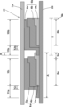
- FIG. 5 is a cross-sectional view of an embodiment of an organic thin-film solar cell.
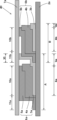
- FIG. 6 is a cross-sectional view of another configuration example of the organic thin-film solar cell according to the embodiment.
- FIG. 7 is a cross-sectional view of another configuration example of the organic thin-film solar cell according to the
- the electronic device includes a plate-like member having one end and the other end in the longitudinal direction, one end and the other end in the lateral direction, a first main surface, and a second main surface.
- the plate-like member can be deformed into a first curved form and a second curved form, and in the first form, the plate-like member is curved so that the first main surface is on the inside and the one end and the other end in the lateral direction approach each other, and in the second form, the plate-like member is curved so that the second main surface is on the inside and the one end and the other end in the longitudinal direction approach each other, and an organic thin-film solar cell is arranged on the surface of the first main surface.
- the electronic device according to the present invention By wrapping the electronic device according to the present invention around an object in the second form, it can be used as a wearable device such as a smart watch or a wristband. In addition, by wrapping the electronic device around an object in the second form, it can be directly provided on a product or used as product packaging, and can be used as smart packaging that has a function of displaying or transmitting the state or change of a product, the state or change of the environment, or other information.
- An embodiment of an electronic device according to the present invention will be described below with reference to the drawings, but the present invention is not limited to these drawings. Also, the same parts are given the same reference numerals to avoid duplicated explanations.
- FIG. 1 is a schematic diagram showing one embodiment of an electronic device according to the present invention, where FIG. 1(a) shows a first form of electronic device E and FIG. 1(b) shows a second form of electronic device E.
- Electronic device E includes a plate-shaped member 101, which has one end x1 and the other end x2 in a longitudinal direction x. Plate-shaped member 101 has one end y1 and the other end y2 in a lateral direction y. Plate-shaped member 101 has a first main surface 111 and a second main surface 121.
- Electronic device E is deformable into a first curved form and a second curved form, and is stable in both the first form and the second form.
- the first main surface 111 of the plate-shaped member 101 is on the inside, and one end y1 and the other end y2 in the short direction y are curved to approach each other. That is, the cross-sectional shape of the plate-shaped member 101 in the short direction y is an arc shape. Note that one end y1 and the other end y2 in the short direction y of the plate-shaped member 101 do not contact each other.
- the second main surface 121 of the plate-shaped member 101 is on the inside, and one end x1 and the other end x2 in the longitudinal direction x are curved to approach each other, and the plate-shaped member 101 is configured in a ring shape.
- one end and the other end in the longitudinal direction x of the plate-shaped member 101 overlap in the region 103, but the one end and the other end in the longitudinal direction x may not overlap, or may be configured so that one end x1 and the other end x2 in the longitudinal direction x butt against each other.
- Electronic device E can be used by wrapping it around the object to which it is to be attached in the second form. In addition, because it can be transformed between the curved first form and the curved second form, it can be easily attached to and detached from the object.
- FIG. 2 is a schematic diagram showing another embodiment of a plate member used in an electronic device according to the present invention, in which FIG. 2(a) shows a first form of the plate member and FIG. 2(b) shows a second form of the plate member.
- the second main surface 121 of the plate member 101 faces inward, and the plate member 101 is curved so that one end x1 and the other end x2 in the longitudinal direction x approach each other, forming a spiral shape.
- the second form in a spiral shape the contact area with the object is increased, improving the winding force.
- the exposed surface of the first main surface 111 of the plate member 101 is increased, and the area for arranging the organic thin-film solar cells 40 is increased, thereby improving the power generation efficiency.
- the plate-shaped member 101 is preferably made of an elastic material.
- the elastic material allows the plate-shaped member 101 to be easily deformed into both the first and second forms.
- the material constituting the plate-shaped member 101 is preferably, for example, metal or resin.
- the metal for example, stainless steel, copper, aluminum, etc. can be used.
- the resin it is preferable to use an elastomer, and as the elastomer, for example, rubbers such as natural rubber, synthetic rubber, silicone rubber, and fluororubber; polyolefin resins such as polyethylene and polypropylene, polystyrene resins, polyurethane resins, polyester resins, polyamide resins, polyvinyl chloride resins, and olefin/alkene resins; etc. can be used.
- the plate-shaped member 101 is preferably made of a metal surface on which a resin (particularly, an elastomer) is laminated. That is, the plate-shaped member 101 is preferably a metal coated with a resin (particularly, an elastomer). By laminating the resin (particularly, an elastomer) on the surface of the metal, the resin (particularly, an elastomer) becomes a cushioning material, and it is possible to prevent the attachment site from being scratched.
- the thickness of the plate-like member 101 cannot be uniformly determined because it is determined based on the type of material, elastic properties, etc., but if the plate-like member 101 is made of metal, the thickness is preferably 0.1 to 0.5 mm, more preferably 0.2 to 0.4 mm, and even more preferably 0.25 to 0.35 mm. If the plate-like member 101 is made of resin, the thickness is preferably 0.5 to 3 mm, more preferably 0.8 to 2.5 mm, and even more preferably 1 to 2 mm.
- the electronic device E has an organic thin-film solar cell 40 on the surface of the first main surface 111 of the plate-shaped member 101. By having the organic thin-film solar cell 40, the electronic device E can be used for a long period of time.
- a plurality of organic thin-film solar cells may be connected in series.
- the longitudinal direction of the organic thin-film solar cell may be perpendicular or parallel to the longitudinal direction x of the plate-shaped member 101. As shown in FIG. 1(a), when the longitudinal direction of the organic thin-film solar cell is perpendicular to the longitudinal direction x of the plate-shaped member 101, even if the plate-shaped member 101 of the first form is changed to the second form, the organic thin-film solar cell is less likely to be damaged because a load is not applied to the organic thin-film solar cell.
- perpendicular to the longitudinal direction x of the plate-shaped member 101 includes a range of ⁇ 20° from the direction perpendicular to the longitudinal direction x, and this range is acceptable, and a right angle (90°) to the longitudinal direction x of the plate-shaped member 101 is preferable.
- the plate-shaped member 101 is configured in a ring shape in the second form as shown in FIG. 1(b), it is preferable that the longitudinal direction of the organic thin-film solar cell is perpendicular to the longitudinal direction x of the plate-shaped member 101.
- Figure 3 shows a schematic diagram of one embodiment of electronic device E in which the longitudinal direction of the organic thin-film solar cell is arranged parallel to the longitudinal direction x of the plate-shaped member 101.
- the number of organic thin-film solar cells in series is reduced, and the connection area for connecting the subcells in series is reduced. Therefore, the area of the active area contributing to power generation can be increased.
- parallel to the longitudinal direction x of the plate-shaped member 101 includes a range of ⁇ 20° with respect to the longitudinal direction x, and this range is acceptable, with 0° with respect to the longitudinal direction x of the plate-shaped member 101 being preferable.
- the longitudinal direction of the organic thin-film solar cell is parallel to the longitudinal direction x of the plate-shaped member 101 as shown in FIG. 3.
- the longitudinal direction of the organic thin-film solar cell may be between perpendicular and parallel to the longitudinal direction x of the plate-shaped member 101. That is, the longitudinal direction of the organic thin-film solar cell may be greater than 20° and less than 70° to the longitudinal direction x of the plate-shaped member 101.
- the longitudinal direction of the organic thin-film solar cell is parallel to the center line of the spiral plate-shaped member 101, which is parallel to the direction in which the plate-shaped member extends spirally.
- the organic thin-film solar cell is least likely to be subjected to a load, and the organic thin-film solar cell is less likely to be damaged.
- the area of the active area that contributes to power generation is also larger than that of the configuration example shown in FIG. 1(a).
- the first embodiment includes, as the organic thin-film solar cell 40, a first laminate including a device substrate, a first electrode at least partially formed on the device substrate, a photovoltaic layer at least partially formed on the first electrode, and a second electrode at least partially formed on the photovoltaic layer, and a second laminate including a first electrode at least partially formed on the device substrate, a photovoltaic layer at least partially formed on the first electrode, and a second electrode at least partially formed on the photovoltaic layer, and the first laminate and the second laminate are formed side by side on the device substrate, and in each of the first laminate and the second laminate, the second electrode has a 2-1 region facing the first electrode and a 2-2 region not facing the first electrode, and it is preferable to use one in which the first electrode of the first laminate is electrically connected to the 2-2 region of the second electrode of the second laminate.
- the organic thin-film solar cell 40 includes a first laminate including a first electrode, a photovoltaic layer at least partially formed on the first electrode, and a second electrode at least partially formed on the photovoltaic layer, and a second laminate including a first electrode, a photovoltaic layer at least partially formed on the first electrode, and a second electrode at least partially formed on the photovoltaic layer, and the first laminate and the second laminate are formed side by side, and in each of the first laminate and the second laminate, the second electrode has a 2-1 region facing the first electrode and a 2-2 region not facing the first electrode, and the first electrode of the first laminate is preferably electrically connected to the 2-2 region of the second electrode of the second laminate.
- the basic configuration of the first aspect will be described with reference to Figures 4 and 5.
- FIG. 4 shows an embodiment of an organic thin-film solar cell that can be suitably used in the present invention, and shows a plan view of an organic thin-film solar cell 40 obtained by attaching multiple organic thin-film solar cells 1a to 1d in series connection to a device substrate 2a.
- FIG. 5 shows a partial cross-sectional view in the thickness direction of the organic thin-film solar cell 40 shown in FIG. 4.
- the organic thin-film solar cell 40 shown in FIG. 4 is composed of organic thin-film solar cells 1a to 1d, and is produced by bonding organic thin-film solar cell 1a and organic thin-film solar cell 1b, organic thin-film solar cell 1b and organic thin-film solar cell 1c, and organic thin-film solar cell 1c and organic thin-film solar cell 1d to a device substrate 2a so that they overlap partially.
- the overlapping portions 30 between the organic thin-film solar cells 1a, 1b, 1c, and 1d correspond to the overlapping portions between the first electrode of one laminate and the second electrode of another laminate, and correspond to the electrically connected portions.
- Figure 4 shows an example of four organic thin-film solar cells connected in series, but the number of organic thin-film solar cells is not limited to this and may be three or less, or five or more.
- the organic thin-film solar cells 1a, 1b, 1c, and 1d are shown bonded to the device substrate 2a, but the organic thin-film solar cells 1a, 1b, 1c, and 1d may also be bonded directly to a plate-shaped member, for example.
- FIG. 5 In the configuration example of the organic thin-film solar cell 40 shown in FIG. 5, a first laminate 6a corresponding to the organic thin-film solar cell A is shown on the left side, and a second laminate 6b corresponding to the organic thin-film solar cell B is shown on the right side. That is, the organic thin-film solar cell 40 shown in FIG.
- a device substrate 2a includes a device substrate 2a, a first electrode 3a at least partially formed on the device substrate 2a, a photovoltaic layer 4a at least partially formed on the first electrode 3a, a first laminate 6a including a second electrode 5a at least partially formed on the photovoltaic layer 4a, a first electrode 3b at least partially formed on the device substrate 2a, a photovoltaic layer 4b at least partially formed on the first electrode 3b, and a second laminate 6b including a second electrode 5b at least partially formed on the photovoltaic layer 4b.
- the first laminate 6a and the second laminate 6b are formed side by side on the device substrate 2a, the second electrode 5a in the first laminate 6a has a 2-1 region 10a facing the first electrode 3a and a 2-2 region 11a not facing the first electrode 3a, and the second electrode 5b in the second laminate 6b has a 2-1 region 10b facing the first electrode 3b and a 2-2 region 11b not facing the first electrode 3b.
- the first electrode 3a of the first laminate 6a is electrically connected to the 2-2 region 11b of the second electrode 5b of the second laminate 6b.
- the 1-1 region 8a, 1-2 region 9a, 2-1 region 10a, and 2-2 region 11a in the first laminate 6a are based on the relative relationship (opposing relationship) between the first electrode 3a and the second electrode 5a included in the first laminate 6a
- the 1-1 region 8b, 1-2 region 9b, 2-1 region 10b, and 2-2 region 11b in the second laminate 6b are based on the relative relationship (opposing relationship) between the first electrode 3b and the second electrode 5b included in the second laminate 6b
- these regions are named based on the relative relationship (opposing relationship) between the first electrode and the second electrode included in each laminate.
- the electrically connected region shown in FIG. 5 means a region where the first electrode 3a of the first laminate 6a and the 2-2 region 11b of the second electrode 5b of the second laminate 6b are electrically conductive.
- the electrically connected region shown in FIG. 5 preferably corresponds to the overlapping portion 30 shown in FIG. 1.
- a plurality of organic thin-film solar cells can be attached to the device substrate 2a to connect the organic thin-film solar cells in series.
- it can be adapted to the shape and size of the electronic device, and it is possible to maximize the power generating area relative to the total area of the power generating laminate provided in the electronic device.
- the wiring resistance can be minimized.
- the overlapping portion 30 has a certain area, it functions stably for a long period of time even if it is deformed by the application of an external force, and the durability of the organic thin-film solar cell 40 can be increased.
- the first electrode 3a of the first laminate 6a has a 1-1 region 8a facing the second electrode 5a and a 1-2 region 9a not facing the second electrode 5a
- the first electrode 3b of the second laminate 6b has a 1-1 region 8b facing the second electrode 5b and a 1-2 region 9b not facing the second electrode 5b
- the 1-2 region 9a in the first electrode 3a of the first laminate 6a is overlapped on the 2-2 region 11b in the second electrode 5b of the second laminate 6b.
- the first electrode and the second electrode can be connected in a planar manner, minimizing wiring resistance.
- the length of the overlapping portion 30 between the 1-2 region 9a in the first electrode 3a of the first laminate 6a and the 2-2 region 11b in the second electrode 5b of the second laminate 6b is preferably long from the viewpoint of reducing the wiring resistance between the first laminate 6a and the second laminate 6b.
- the length of the overlapping portion 30 is longer than the thickness of the second electrode 5b of the second laminate 6b in the same overlapping portion 30, and that the contact resistance between the first electrode 3a of the first laminate 6a and the second electrode 5b of the second laminate 6b is set to be the same as or lower than the wiring resistance value in the overlapping portion 30.
- the length of the overlapping portion 30 is preferably 0.1 mm or more and 5 mm or less, and more preferably 0.2 mm or more and 3 mm or less. This allows multiple organic thin-film solar cells to be connected in series.
- the power-generating laminate even after the power-generating laminate is produced, it can be adapted to the shape and size of the electronic device, and the power generation area relative to the total area of the power-generating laminate provided on the electronic device can be maximized.
- the first electrode and the second electrode can be connected in a planar manner, wiring resistance can be minimized.
- the overlapping portion 30 since the overlapping portion 30 has a certain area, it functions stably for a long period of time even if it is deformed by an external force, and the durability of the organic thin-film solar cell 40 can be increased.
- the distance between adjacent first and second laminates 6a and 6b is preferably 0.01 mm or more and 4 mm or less, more preferably 0.02 mm or more and 3 mm or less, and even more preferably 0.05 mm or more and 2 mm or less, from the viewpoint of maximizing the power generation area relative to the total area of the power generating laminate.
- the first electrode 3a of the first laminate 6a and the second electrode 5b of the second laminate 6b are preferably in contact with each other so that electricity can flow between them, and more preferably the first electrode 3a of the first laminate 6a and the second electrode 5b of the second laminate 6b are in contact due to the stickiness (tack) of the surface of the first electrode 3a of the first laminate 6a and/or the surface of the second electrode 5b of the second laminate 6b, or the weight of the protective layer 7, etc.
- first electrode 3a of the first laminate 6a and the second electrode 5b of the second laminate 6b are more preferably bonded with an adhesive that can conduct electricity (e.g., conductive paste), and more preferably the first electrode 3a of the first laminate 6a and the second electrode 5b of the second laminate 6b are bonded by disposing an adhesive that can conduct electricity in the 1-2 region 9a of the first electrode 3a of the first laminate 6a or the 2-2 region 11b of the second electrode 5b of the second laminate 6b.
- an adhesive that can conduct electricity e.g., conductive paste
- an adhesive that can be electrically conductive e.g., conductive paste
- a mixture of a conductive filler and a resin that acts as an adhesive examples include copper particles, silver particles, gold particles, nickel particles, silver-coated copper particles, silver-coated copper alloy particles, and silver-coated nickel particles.
- resins that can be used as adhesives include epoxy resins, polyurethane resins, acrylic resins, phenolic resins, polyimide resins, and fluororesins. It is preferable to apply the adhesive that can be electrically conductive using a dispenser.
- the components of the organic thin-film solar cell 40 are described in detail below.
- the device substrate 2a is not particularly limited as long as it has flexibility, heat resistance, and the like so that the first electrodes 3a, 3b, the photovoltaic layers 4a, 4b, the second electrodes 5a, 5b, and the like can be formed thereon.
- Materials constituting the device substrate 2a include, for example, organic materials, metal materials, fabric materials, paper materials, etc.
- organic materials include polyester resin, methacrylic resin, methacrylic-maleic acid copolymer resin, polystyrene resin, fluororesin, polyimide resin, fluorinated polyimide resin, polyamide resin, polyamideimide resin, polyetherimide resin, cellulose resin, polyurethane resin, polyetheretherketone resin, polycarbonate resin, alicyclic polyolefin resin, polyarylate resin, polyethersulfone resin, polysulfone resin, cycloolefin resin, polyethylene terephthalate resin, polyethylene naphthalate resin, polyethylene resin, polypropylene resin, and other olefin resins, and polyvinyl chloride resin, polyvinyl alcohol resin, and other vinyl resins.
- metal materials include aluminum and copper that have been given insulating properties.
- fabric materials include nonwoven fabrics and nets.
- paper materials include
- the material constituting the device substrate 2a may be any of the above materials, or may be a combination of the above materials.
- One or more of the organic materials, metal materials, fabric materials, and paper materials may be used. Among them, from the viewpoint of flexibility and heat resistance, organic materials are preferred, and plastic films made of organic materials are more preferred.
- the plastic film preferably has a low water vapor transmission rate. This can improve the durability of the organic thin-film solar cell 40.
- the organic material may have a predetermined glass transition temperature as an index of a predetermined strength, and the glass transition temperature of the organic material is preferably 50°C or higher, more preferably 60°C or higher, and preferably 300°C or lower, more preferably 280°C or lower.
- the glass transition temperature can be calculated based on, for example, JIS K 7121.
- the shape of the device substrate 2a may be, for example, a plate, a film, or a sheet.
- a curved structure may be formed on part or all of the device substrate 2a.
- the thickness of the device substrate 2a is, for example, preferably 0.5 ⁇ m or more and 50 ⁇ m or less, more preferably 1 ⁇ m or more and 20 ⁇ m or less, even more preferably 2 ⁇ m or more and 10 ⁇ m or less, and particularly preferably 3 ⁇ m or more and 8 ⁇ m or less.
- the organic thin-film solar cell 40 has a device substrate 2a.
- the device substrate 2a is made of a material that blocks moisture and ultraviolet rays
- stacking the organic thin-film solar cell 40 having the device substrate 2a on the plate-shaped member 101 can prevent the photovoltaic layer, which will be described later, from coming into contact with moisture or being deteriorated by exposure to ultraviolet rays.
- the organic thin-film solar cell 40 preferably has an adhesive layer between the first electrode 3a and/or the first electrode 3b and the device substrate 2a in one or both of the first laminate 6a and the second laminate 6b.
- the device substrate 2a may be peelable from each of the first laminate 6a and the second laminate 6b so that the first laminate 6a and the second laminate 6b can be attached to a desired object.
- the adhesive layer itself may be a peelable layer, or a peelable layer may be provided separately from the adhesive layer.
- materials for the peelable layer include silicone-based materials and non-silicone-based materials (e.g., acrylic-based materials and urethane-based materials).
- the device substrate 2a is included, but as in the second embodiment, the organic thin-film solar cell 40 does not have to include the device substrate 2a.
- the device substrate 2a may be configured to be peelable from each of the first laminate 6a and the second laminate 6b, and the organic thin-film solar cell 40 from which the device substrate 2a has been peeled from the laminate may be placed directly on the surface of the first main surface 111 of the plate-like member 101.
- a first laminate 6a including a first electrode 3a, a photovoltaic layer 4a at least a part of which is formed on the first electrode 3a, a second electrode 5a at least a part of which is formed on the photovoltaic layer 4a, and a second laminate 6b including a first electrode 3b, a photovoltaic layer 4b at least a part of which is formed on the first electrode 3b, and a second electrode 5b at least a part of which is formed on the photovoltaic layer 4b may be formed on the surface of the first main surface 111 of the plate-shaped member 101.
- the first laminate 6a and the second laminate 6b are formed side by side, and in each of the first laminate 6a and the second laminate 6b, the second electrode has a 2-1 region facing the first electrode and a 2-2 region not facing the first electrode. That is, the second electrode 5a in the first laminate 6a has a 2-1 region 10a facing the first electrode 3a and a 2-2 region 11a not facing the first electrode 3a, and the second electrode 5b in the second laminate 6b has a 2-1 region 10b facing the first electrode 3b and a 2-2 region 11b not facing the first electrode 3b.
- the first electrode 3a of the first laminate 6a may be electrically connected to the 2-2 region 11b of the second electrode 5b of the second laminate 6b.
- the electronic device E has an adhesive layer between the plate-shaped member 101 and one or both of the first electrode 3a of the first laminate 6a and the first electrode 3b of the second laminate 6b.
- the first laminate 6a includes a first electrode 3a, a photovoltaic layer 4a, and a second electrode 5a
- the second laminate 6b includes a first electrode 3b, a photovoltaic layer 4b, and a second electrode 5b.
- the first electrodes 3a, 3b, the photovoltaic layers 4a, 4b, and the second electrodes 5a, 5b may be laminated in this order, or other layers may be formed between the first electrodes 3a, 3b and the photovoltaic layers 4a, 4b, and between the photovoltaic layers 4a, 4b and the second electrodes 5a, 5b.
- Examples of other layers include a hole extraction layer, an electron extraction layer, and an adhesive layer made of a conductive paste.
- a hole extraction layer an electron extraction layer
- an adhesive layer made of a conductive paste.
- the widthwise length of the first laminate 6a and the widthwise length of the second laminate 6b are, for example, preferably 1 cm or more and 100 cm or less, more preferably 2 cm or more and 80 cm or less, even more preferably 5 cm or more and 60 cm or less, and particularly preferably 10 cm or more and 40 cm or less.
- the longitudinal length of the first laminate 6a and the longitudinal length of the second laminate 6b are, for example, preferably 5 cm or more and 200 cm or less, more preferably 10 cm or more and 150 cm or less, even more preferably 15 cm or more and 100 cm or less, and particularly preferably 20 cm or more and 80 cm or less.
- the thickness of the first laminate 6a and the thickness of the second laminate 6b are, for example, preferably 30 nm or more and 3000 nm or less, more preferably 60 nm or more and 2400 nm or less, even more preferably 90 nm or more and 1800 nm or less, and particularly preferably 150 nm or more and 1200 nm or less.
- the first laminate 6a and the second laminate 6b are formed side by side on the device substrate 2a.
- the first electrode 3a of the first laminate 6a has a 1-1 region 8a facing the second electrode 5a of the first laminate 6a and a 1-2 region 9a not facing the second electrode 5a of the first laminate 6a.
- the first electrode 3b of the second laminate 6b has a 1-1 region 8b facing the second electrode 5b of the second laminate 6b and a 1-2 region 9b not facing the second electrode 5b of the second laminate 6b.
- the first electrodes 3a and 3b By providing the first electrodes 3a and 3b with this configuration, it is possible to electrically connect a plurality of laminates in series by providing overlapping portions with the second electrodes 5a and 5b of other laminates. As a result, even after the power generating laminate is produced, it is possible to adapt to the shape and size of the device, and it is possible to maximize the power generating area relative to the total area of the power generating laminate provided in the device. Furthermore, since the first electrode and the second electrode can be connected in a planar manner, the wiring resistance can be minimized.
- the 1-2 region 9a of the first electrode 3a is a region that does not face the second electrode 5a, and may be a region that does not face both the second electrode 5a and the photovoltaic layer 4a.
- the 1-2 region 9b of the first electrode 3b is a region that does not face the second electrode 5b, and may be a region that does not face both the second electrode 5b and the photovoltaic layer 4b.
- the 1-2 region 9a of the first electrode 3a is present on the other widthwise side of the device substrate 2a and is not present on one widthwise side of the device substrate 2a. In other words, it is preferable that the 1-2 region 9a of the first electrode 3a is not present on one side of the 1-1 region 8a (2-1 region 10a) where the first electrode 3a and the second electrode 5a face each other and is present on one side of the 1-1 region 8a (2-1 region 10a). In the second laminate 6b, it is preferable that the 1-2 region 9b of the first electrode 3b is present on the other widthwise side of the device substrate 2a and is not present on one widthwise side of the device substrate 2a.
- the 1-2 region 9b of the first electrode 3b is preferably absent on one side of the 1-1 region 8b (2-1 region 10b) where the first electrode 3b and the second electrode 5b face each other, and is present on one side of the 1-1 region 8b (2-1 region 10b).
- the 1-1 region 8a is larger than the 1-2 region 9a.
- the length ratio of the 1-1 region 8a in the widthwise direction is preferably more than 50% and not more than 90%, more preferably 60% or more and not more than 85%, and even more preferably 65% or more and not more than 80%.
- the 1-1 region 8b is larger than the 1-2 region 9b.
- the length ratio of the 1-1 region 8b in the width direction is preferably more than 50% and not more than 90%, more preferably 60% to 85%, and even more preferably 65% to 80%. With such a length ratio, the inflow and outflow of electrons can be performed successfully in the electrode.
- the length ratio of the width direction of the 1-2 region 9a is preferably 10% or more and less than 50%, more preferably 15% or more and less than 40%, and even more preferably 20% or more and less than 35%.
- the length ratio of the width direction of the 1-2 region 9b is preferably 10% or more and less than 50%, more preferably 15% or more and less than 40%, and even more preferably 20% or more and less than 35%.
- the first laminate 6a and the second laminate 6b respectively, if the 1-2 regions 9a and 9b of the first electrodes 3a and 3b satisfy the length ratio in the above range, an electrically connected portion (overlapping portion) is formed when the organic thin-film solar cell cells are bonded together, so that multiple organic thin-film solar cell cells can be connected in series.
- the power-generating laminate even after the power-generating laminate is produced, it can be adapted to the shape and size of the device, and it is possible to maximize the power generation area relative to the total area of the power-generating laminate provided in the device.
- the first electrode and the second electrode can be connected in a planar manner, wiring resistance can be minimized.
- the durability of the organic thin-film solar cell 40 can be increased by functioning stably for a long period of time even when deformed by the application of external force.
- the second electrode 5a in the first laminate 6a is preferably formed at least partially on the photovoltaic layer 4a and also on the side surface of the photovoltaic layer 4a and the device substrate 2a
- the second electrode 5b in the second laminate 6b is preferably formed at least partially on the photovoltaic layer 4b and also on the side surface of the photovoltaic layer 4b and the device substrate 2a.
- the 2-1 regions 10a, 10b and the 2-2 regions 11a, 11b of the second electrodes 5a, 5b will be described.
- the 2-1 regions 10a, 10b of the second electrodes 5a, 5b correspond to the regions where the first electrodes 3a, 3b and the second electrodes 5a, 5b face each other, similar to the 1-1 regions 8a, 8b of the first electrodes 3a, 3b.
- the 2-1 regions 10a, 10b of the second electrodes and the 1-1 regions 8a, 8b of the first electrodes 3a, 3b may each have the same length or different lengths.
- the 2-2 regions 11a, 11b of the second electrodes 5a, 5b do not face the first electrodes 3a, 3b, and are present on one widthwise side of the device substrate 2a but not on the other widthwise side of the device substrate 2a, and are preferably regions formed only on one widthwise side of the device substrate 2a.
- FIG. 6 shows a cross-sectional view in the thickness direction of another example of the configuration of an organic thin-film solar cell 40.
- the same reference numerals are used to designate the same parts as in FIG. 5 to avoid duplicated description.
- the first laminate is designated by reference numeral 6a
- the second electrode of the first laminate 6a by reference numeral 5a
- the 2-2 region of the second electrode 5a by reference numeral 11a
- the second laminate is designated by reference numeral 6b
- the second electrode of the second laminate 6b by reference numeral 5b the 2-2 region of the second electrode 5b by reference numeral 11b.
- the first laminate and the second laminate are not distinguished, and the laminate is designated by reference numeral 6, the second electrode of the laminate 6 by reference numeral 5, and the 2-2 region of the second electrode 5 by reference numeral 11. The same applies to other parts.
- the 2-2 region 11 is a region of the second electrode 5 that does not face the first electrode 3.
- 11xl indicates the widthwise length of the second electrode 5 that does not face the first electrode 3 and is formed on the photovoltaic layer 4
- 11yl indicates the widthwise length of the second electrode 5 that does not face the first electrode 3 and is formed on the side surface of the photovoltaic layer 4
- 11zl indicates the length obtained by subtracting the sum of the length 11xl and the length 11yl from the widthwise length of the 2-2 region 11.
- 11xh indicates the thickness of the second electrode 5 that is formed on the photovoltaic layer 4
- 11yh indicates the total thickness of the second electrode 5
- 11zh indicates the thickness of the second electrode 5 that is not formed on either the photovoltaic layer 4 or the side surface of the photovoltaic layer 4.
- the second-2 region 11 of the second electrode 5 may include a second-2x region 11x (region surrounded by length 11xl and thickness 11xh in FIG. 6) provided on the photovoltaic layer 4, a second-2y region 11y (region surrounded by length 11yl and thickness 11yh in FIG. 6) provided on the side of the photovoltaic layer 4, and a second-2z region 11z (region surrounded by length 11zl and thickness 11zh in FIG. 6) provided on the device substrate 2.
- the second-2y region 11y is preferably in contact with the side surface of the photovoltaic layer 4 and connects the second-2x region 11x and the second-2z region 11z.
- the side surface of the photovoltaic layer 4 may have a slope (e.g., greater than 0 degrees and less than or equal to 90 degrees) with respect to the lower surface of the photovoltaic layer 4, and if the slope is 90 degrees, the side surface may be perpendicular to the upper and lower surfaces of the photovoltaic layer 4.
- a slope e.g., greater than 0 degrees and less than or equal to 90 degrees
- the second-2y region 11y provided on the side surface of the photovoltaic layer 4 may be shaped like a rectangle, a parallelogram, or the like, and the upper and lower surfaces of the second electrode 5 constituting the second-2y region 11y may have a gradient start point and a gradient end point, and may form a gradient surface.
- the gradient is, for example, greater than 0 degrees and less than or equal to 90 degrees, based on the upper surface of the device substrate 2.
- the gradient start point may be a point close to the device substrate 2, and the gradient end point may be a point far from the device substrate 2.
- the length 11xl may be, for example, the length of a line segment connecting the junction between the lower surface of the second electrode 5 and the upper surface of the photovoltaic layer 4, which corresponds to the junction between the 2-1 region 10 and the 2-2 region 11 of the second electrode 5, and the junction between the upper surface of the photovoltaic layer 4 and the side surface of the photovoltaic layer 4.
- the length 11yl may be, for example, the length of a line segment connecting the junction between the upper surface of the photovoltaic layer 4 and the side surface of the photovoltaic layer 4, and the junction between a plane parallel to the upper surface of the photovoltaic layer 4 and a gradient surface derived from the upper surface of the second electrode 5 (or a length corresponding to the size in the thickness direction of the second electrode 5).
- the length 11yl may be, for example, the length of a line segment connecting two points formed by projecting the gradient start point and gradient end point of the upper surface of the second electrode 5 onto the upper surface of the base layer 2.
- the length 11zl may be, for example, the length of a line segment connecting an end point of the upper surface of the second electrode 5 corresponding to the end point of the 2-2 region 11 and the gradient start point of the upper surface of the second electrode 5.
- the thickness 11xh may be, for example, a height corresponding to the size in the thickness direction of the second electrode 5.
- the thickness 11yh may be, for example, a height corresponding to the size in the thickness direction of the laminate 6 composed of the first electrode 3, the photovoltaic layer 4, and the second electrode 5.
- the thickness 11zh may be, for example, a height corresponding to the size in the thickness direction of the first electrode 3 and/or the second electrode 5.
- the widthwise length of the 2-2x region 11x, the widthwise length of the 2-2y region 11y, and the widthwise length of the 2-2z region 11z satisfy the following relationship.
- the thickness of the 2-1 region 10 and the thickness of the 2-2 region 11 satisfy the following relationship. Thickness of the 2-1 region 10 ⁇ Thickness of the 2-2 region 11
- the thickness of the 2-2x region 11x, the thickness of the 2-2y region 11y, and the thickness of the 2-2z region 11z satisfy the following relationship.
- the 2-2 regions 11a, 11b of the second electrodes 5a, 5b are preferably absent on one side of the 2-1 regions 10a, 10b (1-1 regions 8a, 8b) where the first electrodes 3a, 3b and the second electrodes 5a, 5b face each other, and are present on one side of the 2-1 regions 10a, 10b (1-1 regions 8a, 8b).
- the first electrode and the second electrode can be connected in a planar manner, it is possible to minimize wiring resistance.
- the 2-2 regions 11a, 11b of the second electrodes 5a, 5b preferably include 2-3 regions 12a, 12b that do not face the first electrodes 3a, 3b, do not exist in the width direction of the device substrate 2a, and are formed on the photovoltaic layers 4a, 4b and/or on the side surfaces of the photovoltaic layers 4a, 4b.
- the respective length proportions of the 2-1 regions 10a, 10b and the 2-2 regions 11a, 11b are as follows:
- the 2-1 regions 10a, 10b of the second electrodes 5a, 5b preferably have the longest length among the 2-1 regions 10a, 10b, the 2-2 regions 11a, 11b, and the 2-3 regions 12a, 12b, from the viewpoint of flowing in or sending out electrons between the photovoltaic layers 4a, 4b.
- the length ratio in the width direction of the 2-1 region 10a of the second electrode 5a is preferably 45% to 80%, more preferably 50% to 75%, and even more preferably 55% to 70%, when the total length in the width direction of the 2-1 region 10a and the 2-2 region 11a of the second electrode 5a is taken as 100%. If the length ratio is less than 45%, there is a risk that electrons will not flow in or out successfully between the photovoltaic layer 4a. On the other hand, if the length ratio is more than 80%, there is a risk that the length corresponding to the 2-2 region 11a will be too short.
- the length ratio in the width direction of the 2-1 region 10b of the second electrode 5b is preferably 45% to 80%, more preferably 50% to 75%, and even more preferably 55% to 70%, when the total length in the width direction of the 2-1 region 10b and the 2-2 region 11b of the second electrode 5b is taken as 100%. If the length ratio is less than 45%, there is a risk that electrons cannot be successfully flowed in or sent out between the photovoltaic layer 4b. On the other hand, if the length ratio is more than 80%, there is a risk that the length corresponding to the 2-2 region 11b will be too short.
- the 2-2 regions 11a, 11b of the second electrodes 5a, 5b are formed in the width direction of the device substrate 2a, and may have a length shorter than the length in the width direction of the 2-1 regions 10a, 10b from the viewpoint of ensuring a bonding portion with other organic thin-film solar cells.
- the length ratio in the width direction of the 2-2 region 11a of the second electrode 5a is preferably 20% or more and 55% or less, more preferably 25% or more and 50% or less, and even more preferably 30% or more and 45% or less, when the total length of the 2-1 region 10a of the second electrode 5a and the 2-2 region 11a in the width direction is taken as 100%. If the length ratio is less than 20%, there is a risk that the bonding portion with other organic thin-film solar cells cannot be secured. On the other hand, if the length ratio is more than 55%, there is a risk that the flow or sending of electrons between the photovoltaic layer 4a cannot be successfully performed.
- the 2-2 region 11a of the second electrode 5a satisfies the length ratio in the above range, a portion (overlap portion) electrically connected to the organic thin-film solar cell is formed, so that multiple organic thin-film solar cells can be connected in series.
- the power generating laminate even after the power generating laminate is produced, it can be adapted to the shape and size of the electronic device, and it is possible to maximize the power generating area relative to the total area of the power generating laminate provided in the electronic device.
- the first electrode and the second electrode can be connected in a planar manner, wiring resistance can be minimized.
- the durability of the organic thin-film solar cell 40 can be improved by functioning stably for a long period of time even if it is deformed by the application of external force.
- the length ratio in the width direction of the 2-2 region 11b of the second electrode 5b is preferably 20% or more and 55% or less, more preferably 25% or more and 50% or less, and even more preferably 30% or more and 45% or less, when the total length of the 2-1 region 10b and the 2-2 region 11b of the second electrode 5b in the width direction is taken as 100%. If the length ratio is less than 20%, there is a risk that the bonding portion with other organic thin-film solar cells cannot be secured. On the other hand, if the length ratio is more than 55%, there is a risk that the flow or sending of electrons between the photovoltaic layer 4b cannot be successfully performed.
- the 2-2 region 11b of the second electrode 5b satisfies the length ratio in the above range, a portion (overlap portion) electrically connected to the organic thin-film solar cell is formed, so that multiple organic thin-film solar cells can be connected in series.
- the power generating laminate even after the power generating laminate is produced, it can be adapted to the shape and size of the electronic device, and it is possible to maximize the power generating area relative to the total area of the power generating laminate provided in the electronic device.
- the first electrode and the second electrode can be connected in a planar manner, wiring resistance can be minimized.
- the durability of the organic thin-film solar cell 40 can be improved by functioning stably for a long period of time even if it is deformed by the application of external force.
- the 2-3 regions 12a and 12b of the second electrodes 5a and 5b are preferably formed on the photovoltaic layers 4a and 4b and/or on the side surfaces of the photovoltaic layers 4a and 4b.
- the length ratio in the width direction of the 2-3 region 12a of the second electrode 5a is preferably 10% to 25%, more preferably 12% to 23%, and even more preferably 14% to 21%, when the total length in the width direction of the 2-1 region 10a and the 2-2 region 11a of the second electrode 5a is taken as 100%. If the length ratio is less than 10%, there is a risk that the region formed on the side surface of the photovoltaic layer 4a cannot be secured. On the other hand, if the length ratio is more than 25%, there is a risk that the flow or send-out of electrons between the photovoltaic layer 4a and the photovoltaic layer 4a cannot be successfully achieved, and that the bonding portion with other organic thin-film solar cells cannot be secured.
- the length ratio in the width direction of the 2-3 region 12b of the second electrode 5b is preferably 10% to 25%, more preferably 12% to 23%, and even more preferably 14% to 21%, when the total length in the width direction of the 2-1 region 10b and the 2-2 region 11b of the second electrode 5b is taken as 100%. If the length ratio is less than 10%, there is a risk that the region formed on the side surface of the photovoltaic layer 4b cannot be secured. On the other hand, if the length ratio is more than 25%, there is a risk that the flow or send-out of electrons between the photovoltaic layer 4b and the photovoltaic layer 4b cannot be successfully achieved, and that the bonding portion with other organic thin-film solar cells cannot be secured.
- the 2-2 regions 11a, 11b of the second electrodes 5a, 5b and the 1-2 regions 9a, 9b of the first electrodes 3a, 3b are preferably present on one side and the other side in the width direction of the device substrate 2a.
- the 2-2 regions 11a, 11b of the second electrodes 5a, 5b and the 1-2 regions 9a, 9b of the first electrodes 3a, 3b are preferably present on the device substrate 2a at a distance equal to or greater than the distance between both ends of the 2-1 regions 10a, 10b and the 1-1 regions 8a, 8b.
- the 2-2 regions 11a, 11b of the second electrodes 5a, 5b and the 1-2 regions 9a, 9b of the first electrodes 3a, 3b may have the same length or different lengths.
- each of the first laminate 6a and the second laminate 6b it is preferable that one of the first electrodes 3a, 3b and the second electrodes 5a, 5b is a negative electrode (anode) and the other is a positive electrode (cathode). It is also preferable that at least the second electrodes 5a, 5b are optically transparent, and it is more preferable that both the second electrodes 5a, 5b and the first electrodes 3a, 3b are optically transparent.
- the first electrodes 3a, 3b and the second electrodes 5a, 5b may be a single-layer structure using a conductive material, or may be a laminate structure of two or more layers.
- the negative electrode is an electrode made of a conductive material with a high work function, through which electrons flow to an external circuit.
- materials that make up the negative electrode include metal oxides such as nickel oxide, tin oxide, indium oxide, indium tin oxide (ITO), indium zirconium oxide (IZO), titanium oxide, indium oxide, or zinc oxide; metals such as gold, platinum, silver, chromium, or cobalt, and alloys thereof.
- materials that make up the negative electrode include PEDOT:PSS, a polythiophene derivative doped with polystyrene sulfonic acid, and conductive polymer materials such as polypyrrole or polyaniline doped with iodine.
- the negative electrode is a transparent electrode
- a translucent metal oxide such as ITO, zinc oxide, or tin oxide
- ITO indium tin oxide
- the thickness of the negative electrode among the first electrodes 3a, 3b or the second electrodes 5a, 5b is, for example, preferably 10 nm or more and 1000 nm or less, more preferably 20 nm or more and 800 nm or less, even more preferably 30 nm or more and 600 nm or less, and particularly preferably 50 nm or more and 400 nm or less.
- the thickness of the negative electrode is within the above range, light can be efficiently converted into electricity without reducing the light transmittance.
- the width and length of the negative electrode among the first electrodes 3a, 3b or the second electrodes 5a, 5b may be the same as the width and length of the first laminate 6a and the second laminate 6b.
- the electrode that is the negative electrode among the first electrodes 3a, 3b or the second electrodes 5a, 5b may have a predetermined sheet resistance, and the value of the sheet resistance is, for example, preferably 1 ⁇ / ⁇ or more and 1000 ⁇ / ⁇ or less, more preferably 2 ⁇ / ⁇ or more and 500 ⁇ / ⁇ or less, and even more preferably 5 ⁇ / ⁇ or more and 100 ⁇ / ⁇ or less.
- the negative electrode of the first electrodes 3a, 3b or the second electrodes 5a, 5b may be formed using, for example, a vacuum film-forming method such as vapor deposition or sputtering, or a wet coating method in which an ink containing nanoparticles or the like is applied to form a film, and may be etched or otherwise shaped as required.
- a vacuum film-forming method such as vapor deposition or sputtering
- a wet coating method in which an ink containing nanoparticles or the like is applied to form a film, and may be etched or otherwise shaped as required.
- the positive electrode is an electrode made of a conductive material with a low work function into which electrons flow.
- materials that make up the positive electrode include metals such as platinum, gold, silver, copper, iron, tin, zinc, aluminum, indium, chromium, lithium, sodium, potassium, cesium, calcium, and magnesium, and alloys thereof; inorganic salts such as lithium fluoride and cesium fluoride; and metal oxides such as nickel oxide, aluminum oxide, lithium oxide, and cesium oxide.
- Preferred materials that make up the positive electrode are metals such as platinum, gold, silver, copper, iron, tin, aluminum, calcium, and indium, and alloys of the above metals such as indium tin oxide.
- the thickness of the positive electrode among the first electrodes 3a, 3b or the second electrodes 5a, 5b is, for example, preferably 10 nm or more and 1000 nm or less, more preferably 20 nm or more and 800 nm or less, even more preferably 30 nm or more and 600 nm or less, and particularly preferably 50 nm or more and 400 nm or less.
- the thickness of the positive electrode is within the above range, light can be efficiently converted into electricity without reducing the light transmittance.
- the width and length of the positive electrode among the first electrodes 3a, 3b or the second electrodes 5a, 5b may be the same as the width and length of the first laminate 6a and the second laminate 6b.
- the electrode that is the positive electrode among the first electrodes 3a, 3b or the second electrodes 5a, 5b may have a predetermined sheet resistance, and the value of the sheet resistance is, for example, preferably 1 ⁇ / ⁇ or more and 1000 ⁇ / ⁇ or less, more preferably 2 ⁇ / ⁇ or more and 500 ⁇ / ⁇ or less, and even more preferably 5 ⁇ / ⁇ or more and 100 ⁇ / ⁇ or less.
- the electrode that is to be the positive electrode out of the first electrodes 3a, 3b or the second electrodes 5a, 5b may be formed using, for example, a vacuum film-forming method such as a vapor deposition method or a sputtering method, or a wet coating method in which a film is formed by applying an ink containing nanoparticles or the like, and may be etched, etc., to a predetermined shape as necessary.
- a vacuum film-forming method such as a vapor deposition method or a sputtering method
- a wet coating method in which a film is formed by applying an ink containing nanoparticles or the like, and may be etched, etc., to a predetermined shape as necessary.
- the negative and positive electrodes may each use one or more materials in each layer, may have a laminated structure of two or more layers, and other layers may be formed in the negative and positive electrodes.
- Materials used in the other layers may be poly(ethylenedioxythiophene):poly(styrenesulfonic acid) (PEDOT:PSS), molybdenum oxide, lithium fluoride, 2,9-dimethyl-4,7-diphenyl-1,10-phenanthroline, etc.
- At least one of the first electrodes 3a, 3b and the second electrodes 5a, 5b is preferably optically transparent, and more preferably has a light transmittance of 40% or more, more preferably 55% or more, even more preferably 85% or more, and even more preferably 90% or more in the wavelength range of 360 to 830 nm.
- the electrode may be formed using the above-mentioned metal oxide or an alloy thereof.
- Photovoltaic Layer At least a portion of the photovoltaic layer 4a of the first laminate 6a is formed on the first electrode 3a, and at least a portion of the photovoltaic layer 4b of the second laminate 6b is formed on the first electrode 3b.
- the photovoltaic layers 4a, 4b are formed on the first electrodes 3a, 3b, and are preferably also formed on the device substrate 2a.
- Examples of materials constituting the photovoltaic layers 4a and 4b include organic dye materials and organic semiconductor materials.
- the materials constituting the photovoltaic layers 4a and 4b are preferably organic semiconductor materials from the viewpoints of light weight, flexibility, etc.
- the photovoltaic layers 4a and 4b are preferably thin films containing organic semiconductor materials.
- Organic semiconductor materials are broadly divided into p-type and n-type, but because the holes and electrons that contribute to electrical conduction change depending on the electronic state, doping state, and trap state of the material, it is sometimes not possible to clearly classify them as p-type or n-type, and the same material may exhibit both p-type and n-type properties.
- the p-type semiconductor may be, for example, a polymer organic semiconductor compound, a low molecular weight organic semiconductor compound, etc.
- polymeric organic semiconductor compounds include conjugated polymer semiconductor compounds such as polythiophene, polyfluorene, polyphenylene vinylene, polythienylene vinylene, polyacetylene, and polyaniline; polymeric semiconductor compounds such as substituted oligothiophenes; and semiconductor compounds in which two or more monomers are copolymerized.
- the polymeric organic semiconductor compound may be one type of compound or a mixture of two or more types of compounds.
- low molecular weight organic semiconductor compounds include condensed aromatic hydrocarbons such as naphthacene, pentacene, and pyrene; oligothiophenes containing four or more thiophene rings; compounds containing one or more selected from thiophene rings, benzene rings, fluorene rings, naphthalene rings, anthracene rings, thiazole rings, thiadiazole rings, and benzothiazole rings, with a total of four or more connected; macrocyclic compounds such as phthalocyanine compounds, metal complexes thereof, porphyrin compounds such as tetrabenzoporphyrin, and metal complexes thereof, etc.
- the molecular weight of the low molecular weight organic semiconductor compound is, for example, preferably 100 or more and 5000 or less, and more preferably 200 or more and 2000 or less.
- the n-type semiconductor may be, for example, a fullerene compound, a quinolinol derivative metal complex such as 8-hydroxyquinoline aluminum; a condensed ring tetracarboxylic acid diimide such as naphthalene tetracarboxylic acid diimide or perylene tetracarboxylic acid diimide; a perylene diimide derivative; a terpyridine metal complex, a tropolone metal complex, a flavonol metal complex, a perinone derivative, a benzimidazole derivative, a benzoxazole derivative, a thiazole derivative, a benzthiazole derivative, a benzothiadiazole derivative, an oxadiazole derivative, a thiadiazole derivative, a triazole derivative, a pyrazine derivative, a phenanthroline derivative, a quinoxaline derivative, a benzoquinoline derivative, a borane derivative, an anthrac
- the photovoltaic layers 4a and 4b preferably contain at least a p-type semiconductor and an n-type semiconductor.
- the n-type and p-type semiconductors used in the photovoltaic layers 4a and 4b may be one type or two or more types.
- the photovoltaic layers 4a and 4b may have a single-layer structure or a laminated structure of two or more layers.
- the photovoltaic layers 4a and 4b may contain, for example, an n-type semiconductor and a p-type semiconductor in the same layer, or may contain an n-type semiconductor and a p-type semiconductor in separate layers.
- Examples of the configuration of the photovoltaic layers 4a and 4b include a bulk heterojunction type having a layer (i layer) in which a p-type semiconductor and an n-type semiconductor are separated within the layer, a stacked type (hetero pn junction type) in which a layer containing a p-type semiconductor (p layer) and a layer containing an n-type semiconductor (n layer) have an interface, a Schottky type, and combinations of these.
- the thickness of the photovoltaic layers 4a and 4b is, for example, preferably 10 nm or more and 1000 nm or less, more preferably 20 nm or more and 500 nm or less, and even more preferably 50 nm or more and 300 nm or less.
- the widthwise length of the photovoltaic layers 4a, 4b may be the same as the widthwise length of the first laminate 6a and the second laminate 6b.
- the length in the longitudinal direction of the photovoltaic layers 4a, 4b may be the same as the length in the longitudinal direction of the first laminate 6a and the second laminate 6b.
- the photovoltaic layers 4a and 4b are preferably formed by a coating method, and more preferably by a wet coating method.
- coating methods include spin coating, reverse roll coating, gravure coating, kiss coating, spray coating, air knife coating, impregnation coating, and curtain coating.
- Protective Layer A protective layer 7a is preferably disposed on the second electrode 5a of the first laminate 6a and on the second electrode 5b of the second laminate 6b.
- the protective layer 7a is preferably a layer that protects the first laminate 6a and the second laminate 6b from corrosion due to temperature, humidity, natural light, wind and rain, etc., and prevents deterioration.
- Examples of materials constituting the protective layer 7a include polyethylene resin, polypropylene resin, cyclic olefin resin, acrylonitrile-styrene resin, acrylonitrile-butadiene-styrene resin, polyvinyl chloride resin, fluororesin, polyester resins such as polyethylene terephthalate resin and polyethylene naphthalate resin, phenol resin, polyacrylic resin, polyamide resin, polyimide resin, polyurethane resin, silicone resin, etc.
- the protective layer 7a is weather resistant, it is preferable that the protective layer 7a is a fluororesin.
- fluororesins include polytetrafluoroethylene, 4-fluoroethylene-perchloroalkoxy copolymer, 4-fluoroethylene-6-fluoropropylene copolymer, 2-ethylene-4-fluoroethylene copolymer, polyvinylidene fluoride, polyvinyl fluoride, and the like.
- the protective layer 7a may be made of one type of material, or may be made of two or more types of materials.
- the protective layer 7a may be one layer, or two or more layers.
- the thickness of the protective layer 7a is, for example, preferably 0.5 ⁇ m to 100 ⁇ m, more preferably 1 ⁇ m to 50 ⁇ m, and even more preferably 2 ⁇ m to 30 ⁇ m. The thinner the protective layer, the higher the flexibility. When the protective layer 7a is two or more layers, the thickness of the protective layer 7a refers to the total thickness.
- the protective layer 7a is preferably transparent to visible light.
- the light transmittance of the protective layer 7a in the visible light range of wavelengths from 360 to 830 nm is preferably 80% or more, more preferably 90% or more, and even more preferably 95% or more.
- the protective layer 7a may be formed on the second electrodes 5a, 5b via an adhesive layer, similar to the device substrate 2a.
- the protective layer 7a may be peelable, similar to the device substrate 2a.
- the adhesive layer provided between the protective layer 7a and the second electrodes 5a, 5b may be a peelable layer, or a peelable layer may be provided separately from the adhesive layer.
- the adhesive layer and/or peeling layer arranged between the device substrate 2a and the first electrodes 3a, 3b and the adhesive layer and/or peeling layer arranged between the protective layer 7a and the second electrodes 5a, 5b preferably have different peeling strengths. From the viewpoint of easily attaching to an attachment target (e.g., the plate-like member 101 in the second embodiment), it is more preferable that the peeling strength of the adhesive layer and/or peeling layer arranged between the protective layer 7a and the second electrodes 5a, 5b is greater than the peeling strength of the adhesive layer and/or peeling layer arranged between the device substrate 2a and the first electrodes 3a, 3b. This makes it easier for the device substrate 2a to be peeled off before the protective layer 7a, and the first electrodes 3a, 3b, etc. can be attached directly to the object.
- the protective layer 7a and the device substrate 2a may have a predetermined rigidity (e.g., bending rigidity). It is preferable that the protective layer 7a and the device substrate 2a have different rigidities, and it is more preferable that the rigidity of the protective layer 7a is greater than the rigidity of the device substrate 2a.
- a predetermined rigidity e.g., bending rigidity
- FIG. 7 shows a cross-sectional view in the thickness direction of another example of the configuration of an organic thin-film solar cell 40.
- FIG. 7 A configuration example X of the first stack 6a and the second stack 6b in the organic thin-film solar cell 40 will be described with reference to Fig. 7.
- the first stack 6a includes a first electrode 3a, a photovoltaic layer 4a, and a second electrode 5a, in that order, on the device substrate 2a
- the second stack 6b includes a first electrode 3b, a photovoltaic layer 4b, and a second electrode 5b, in that order, on the device substrate 2a.
- the first electrode 3a of the first laminate 6a has a 1-1 region 8a facing the second electrode 5a of the first laminate 6a and a 1-2 region 9a not facing the second electrode 5a of the first laminate 6a
- the second electrode 5a of the first laminate 6a has a 2-1 region 10a facing the first electrode 3a of the first laminate 6a and a 2-2 region 11a not facing the first electrode 3a of the first laminate 6a.
- the first electrode 3b of the second laminate 6b has a 1-1 region 8b facing the second electrode 5b of the second laminate 6b and a 1-2 region 9b not facing the second electrode 5b of the second laminate 6b
- the second electrode 5b of the second laminate 6b has a 2-1 region 10b facing the first electrode 3b of the second laminate 6b and a 2-2 region 11b not facing the first electrode 3b of the second laminate 6b.
- the 2-2 region 11b of the second electrode 5b of the second laminate 6b forms an overlapping portion 30 with the 1-2 region 9a of the first electrode 3a of the first laminate 6a, and is electrically connected.
- the 2-2 region 11a of the second electrode 5a of the first laminate 6a is also formed on the side surface of the photovoltaic layer 4a and on the device substrate 2a.
- the 1-2 region 9a of the first electrode 3a of the first laminate 6a is formed on the side surface of the second electrode 5b of the second laminate 6b and on the second electrode 5b.
- the configuration examples of the first laminate 6a and the second laminate 6b in the organic thin-film solar cell 40 have been given.
- the organic thin-film solar cell 40 includes three or more laminates, it is preferable to use one or more configuration examples selected from the configuration example shown in FIG. 5 and the configuration example X.
- the organic thin-film solar cell 40 may be fabricated by arranging each laminate using a combination of only the configuration example shown in FIG. 5, a combination of only the configuration example X, or a combination of the configuration example shown in FIG. 5 and the configuration example X.
- the organic thin-film solar cells 40 can be connected in series, and even after the power generating laminate is fabricated, it is possible to conform to the shape and size of the device, and it is possible to maximize the power generation area relative to the total area of the power generating laminate provided in the device.
- the first electrode and the second electrode can be connected in a planar manner, the wiring resistance can be minimized.
- the electrically connected parts (overlapping parts) of the laminates can withstand deformation due to external forces.
- the electronic device E preferably has electrodes for measuring biological information arranged on the second main surface 121 of the plate-like member 101.
- the electrodes for measuring biological information come into direct contact with the skin of the subject. This makes it possible to detect electrical signals from the subject's body and measure biological information.
- the electronic unit calculates and processes the electrical signals acquired by the biometric measurement electrodes to obtain information on the body, such as electrocardiogram, heart rate, pulse rate, respiratory rate, blood pressure, body temperature, electromyogram, and sweating.
- an electrode capable of measuring an electrocardiogram is preferable.
- An electrocardiogram is an electrical change caused by the movement of the heart, and information detected through electrodes on the surface of a living body and recorded as a waveform is called an electrocardiogram.
- An electrocardiogram is generally recorded as a waveform in which time is plotted on the horizontal axis and potential difference is plotted on the vertical axis.
- the waveform of each heartbeat appearing on an electrocardiogram is mainly composed of five representative waves, namely, a P wave, a Q wave, an R wave, an S wave, and a T wave, and a U wave is also present.
- the period from the beginning of the Q wave to the end of the S wave is sometimes called a QRS wave.
- a bioinformation measuring electrode capable of detecting at least an R wave is preferable.
- the heart rate can also be measured. That is, the time from the peak of an R wave to the peak of the next R wave is generally called the RR interval (seconds), and the heart rate per minute can be calculated based on the following formula.
- the electronic device E preferably has a sensor disposed on the first main surface 111 and/or the second main surface 121 of the plate-like member 101.
- the sensor include a sensor that can measure environmental information such as temperature, humidity, air pressure, and altitude, and a sensor that can measure position information using GPS.
- the sensor may be arranged on either the first main surface 111 or the second main surface 121 of the plate-shaped member 101, or on both the first main surface 111 and the second main surface 121 of the plate-shaped member 101.
- the electronic device E preferably has an image display device disposed on the first main surface 111 of the plate-like member 101.
- an image display device By disposing the image display device, information measured by the electrodes and sensors for measuring biological information can be displayed on the image display device, making it easier to grasp the condition of the object.
- the image display device can display necessary information.
- image display devices include liquid crystal display devices, electroluminescence (EL) display panels, plasma display panels (PDPs), field emission displays (FEDs), QLEDs, microLEDs, etc.
- the image display device is, for example, a liquid crystal display device
- the image display unit can be configured to have an optical film along with components such as a liquid crystal cell, a polarizing plate, and a backlight.
- the electronic device E may be used as a wearable device.
- the electronic device E may be used as a wristband worn around the wrist, an armband worn around the arm, a smart watch, etc.
- the electronic device E may be directly attached to a product or may be used as product packaging.
- the electronic device E may be used as smart packaging that has the function of displaying or transmitting the state or change of a product, the state or change of the environment, or other information.
- electronic device E can be transformed into a first curved form and a second curved form, so the position at which it is attached to the object can be easily changed.
- electronic device E can be easily attached to and detached from the object.
- electronic device E can be easily attached to and detached from the object, it can be reused and re-used.
- the curved second form since a force is always applied in the wrapping direction, it can be easily attached to objects having a variety of shapes, including not only circular shapes but also triangular and rectangular shapes (e.g., square). Furthermore, when the electronic device E is attached to an object, it is easy to maintain its position, so it can be attached for a long period of time. Even if the object expands or contracts, the shape of the electronic device E easily follows the changes in the object's shape, so it can be measured for a long period of time. Examples of objects that expand or contract include a pulsating hose pump, the abdominal circumference of a four-legged animal, and plants such as trees.
- Electronic device E can be attached to a push-type hand soap container when used. For example, if a liquid level sensor is provided in electronic device E and this electronic device E is attached to a hand soap container, the electronic device E can detect the amount of hand soap remaining in the container. When electronic device E detects that the amount of hand soap remaining has fallen below a predetermined value, the container can be refilled with hand soap. When replacing the container, electronic device E can be removed from the container and reused by attaching the removed electronic device E to another container.
Landscapes
- Physics & Mathematics (AREA)
- Electromagnetism (AREA)
- Engineering & Computer Science (AREA)
- Textile Engineering (AREA)
- Mechanical Engineering (AREA)
- Photovoltaic Devices (AREA)
Priority Applications (1)
| Application Number | Priority Date | Filing Date | Title |
|---|---|---|---|
| JP2024515710A JPWO2024085106A1 (https=) | 2022-10-17 | 2023-10-16 |
Applications Claiming Priority (2)
| Application Number | Priority Date | Filing Date | Title |
|---|---|---|---|
| JP2022166103 | 2022-10-17 | ||
| JP2022-166103 | 2022-10-17 |
Publications (1)
| Publication Number | Publication Date |
|---|---|
| WO2024085106A1 true WO2024085106A1 (ja) | 2024-04-25 |
Family
ID=90737791
Family Applications (1)
| Application Number | Title | Priority Date | Filing Date |
|---|---|---|---|
| PCT/JP2023/037370 Ceased WO2024085106A1 (ja) | 2022-10-17 | 2023-10-16 | 電子デバイス |
Country Status (2)
| Country | Link |
|---|---|
| JP (1) | JPWO2024085106A1 (https=) |
| WO (1) | WO2024085106A1 (https=) |
Citations (6)
| Publication number | Priority date | Publication date | Assignee | Title |
|---|---|---|---|---|
| JP2011018890A (ja) * | 2009-06-11 | 2011-01-27 | Dainippon Printing Co Ltd | 有機薄膜太陽電池およびその製造方法 |
| JP2012129229A (ja) * | 2010-12-13 | 2012-07-05 | Konica Minolta Holdings Inc | 有機エレクトロニクスパネルの製造方法 |
| US20130044215A1 (en) * | 2011-08-17 | 2013-02-21 | Apple Inc. | Bi-stable spring with flexible display |
| JP2016526417A (ja) * | 2013-06-21 | 2016-09-05 | エムシー10 インコーポレイテッドMc10,Inc. | 形状適合する電子装置を有するバンド |
| JP2016167511A (ja) * | 2015-03-09 | 2016-09-15 | 株式会社東芝 | 太陽電池モジュールおよびその製造方法 |
| KR20180006767A (ko) * | 2016-07-11 | 2018-01-19 | 이효정 | 결제 기능 부가 슬랩 밴드 및 이의 구동 방법 |
-
2023
- 2023-10-16 JP JP2024515710A patent/JPWO2024085106A1/ja active Pending
- 2023-10-16 WO PCT/JP2023/037370 patent/WO2024085106A1/ja not_active Ceased
Patent Citations (6)
| Publication number | Priority date | Publication date | Assignee | Title |
|---|---|---|---|---|
| JP2011018890A (ja) * | 2009-06-11 | 2011-01-27 | Dainippon Printing Co Ltd | 有機薄膜太陽電池およびその製造方法 |
| JP2012129229A (ja) * | 2010-12-13 | 2012-07-05 | Konica Minolta Holdings Inc | 有機エレクトロニクスパネルの製造方法 |
| US20130044215A1 (en) * | 2011-08-17 | 2013-02-21 | Apple Inc. | Bi-stable spring with flexible display |
| JP2016526417A (ja) * | 2013-06-21 | 2016-09-05 | エムシー10 インコーポレイテッドMc10,Inc. | 形状適合する電子装置を有するバンド |
| JP2016167511A (ja) * | 2015-03-09 | 2016-09-15 | 株式会社東芝 | 太陽電池モジュールおよびその製造方法 |
| KR20180006767A (ko) * | 2016-07-11 | 2018-01-19 | 이효정 | 결제 기능 부가 슬랩 밴드 및 이의 구동 방법 |
Also Published As
| Publication number | Publication date |
|---|---|
| JPWO2024085106A1 (https=) | 2024-04-25 |
Similar Documents
| Publication | Publication Date | Title |
|---|---|---|
| Zou et al. | Flexible devices: from materials, architectures to applications | |
| KR101700989B1 (ko) | 유기 전자 디바이스 및 그 제조 방법 | |
| Pang et al. | Recent advances in flexible sensors for wearable and implantable devices | |
| KR101316479B1 (ko) | 전극 제조 방법 | |
| JP2015082611A (ja) | 太陽電池一体型融雪シート、及び太陽電池一体型融雪シートの設置方法 | |
| WO2016158791A1 (ja) | 有機薄膜太陽電池モジュール | |
| JP2012080060A (ja) | 有機太陽電池モジュール | |
| US20190363206A1 (en) | Semiconductor device | |
| Yu et al. | Highly flexible polymer light-emitting devices using carbon nanotubes as both anodes and cathodes | |
| JP2016225628A (ja) | 有機薄膜太陽電池モジュール | |
| WO2024085106A1 (ja) | 電子デバイス | |
| JP2009032983A (ja) | 有機薄膜受光素子、その有機薄膜受光素子を用いた有機薄膜受発光素子、その有機薄膜受発光素子を用いた脈拍センサー、および、その脈拍センサーをステアリングに配設した車両 | |
| JP6558022B2 (ja) | 薄膜太陽電池モジュール | |
| CN117377333A (zh) | 光电转换器件 | |
| JP5621657B2 (ja) | 太陽電池モジュール | |
| JP2016058606A (ja) | 太陽電池モジュール | |
| JP2016189466A (ja) | 有機薄膜太陽電池モジュール | |
| JP2017228743A (ja) | 太陽電池モジュール、太陽電池モジュール巻回体及び太陽電池装着物 | |
| KR20090100684A (ko) | 에너지 수집형 전력원을 구비한 웨어러블 장치 | |
| WO2022230707A1 (ja) | 高分子圧電性フィルム素子と、それを用いた蓄電デバイスおよび荷重検知デバイス | |
| JP2015088674A (ja) | 有機電子デバイスモジュール | |
| TWI804558B (zh) | 有機器件用電極基板材料及其製造方法 | |
| JP2015090935A (ja) | 薄膜太陽電池モジュール及び薄膜太陽電池アレイ | |
| JP2016047003A (ja) | 太陽電池モジュール | |
| NAKAJIMA et al. | Efficiency Advancements and Mechanical Durability of Ultrathin Flexible Organic Photovoltaics |
Legal Events
| Date | Code | Title | Description |
|---|---|---|---|
| ENP | Entry into the national phase |
Ref document number: 2024515710 Country of ref document: JP Kind code of ref document: A |
|
| 121 | Ep: the epo has been informed by wipo that ep was designated in this application |
Ref document number: 23879749 Country of ref document: EP Kind code of ref document: A1 |
|
| NENP | Non-entry into the national phase |
Ref country code: DE |
|
| 122 | Ep: pct application non-entry in european phase |
Ref document number: 23879749 Country of ref document: EP Kind code of ref document: A1 |