WO2024079997A1 - 液晶光シャッタおよび撮像装置 - Google Patents
液晶光シャッタおよび撮像装置 Download PDFInfo
- Publication number
- WO2024079997A1 WO2024079997A1 PCT/JP2023/030332 JP2023030332W WO2024079997A1 WO 2024079997 A1 WO2024079997 A1 WO 2024079997A1 JP 2023030332 W JP2023030332 W JP 2023030332W WO 2024079997 A1 WO2024079997 A1 WO 2024079997A1
- Authority
- WO
- WIPO (PCT)
- Prior art keywords
- light
- liquid crystal
- mask
- transparent electrode
- electrode layer
- Prior art date
- Legal status (The legal status is an assumption and is not a legal conclusion. Google has not performed a legal analysis and makes no representation as to the accuracy of the status listed.)
- Ceased
Links
Images







Classifications
-
- G—PHYSICS
- G02—OPTICS
- G02F—OPTICAL DEVICES OR ARRANGEMENTS FOR THE CONTROL OF LIGHT BY MODIFICATION OF THE OPTICAL PROPERTIES OF THE MEDIA OF THE ELEMENTS INVOLVED THEREIN; NON-LINEAR OPTICS; FREQUENCY-CHANGING OF LIGHT; OPTICAL LOGIC ELEMENTS; OPTICAL ANALOGUE/DIGITAL CONVERTERS
- G02F1/00—Devices or arrangements for the control of the intensity, colour, phase, polarisation or direction of light arriving from an independent light source, e.g. switching, gating or modulating; Non-linear optics
- G02F1/01—Devices or arrangements for the control of the intensity, colour, phase, polarisation or direction of light arriving from an independent light source, e.g. switching, gating or modulating; Non-linear optics for the control of the intensity, phase, polarisation or colour
- G02F1/13—Devices or arrangements for the control of the intensity, colour, phase, polarisation or direction of light arriving from an independent light source, e.g. switching, gating or modulating; Non-linear optics for the control of the intensity, phase, polarisation or colour based on liquid crystals, e.g. single liquid crystal display cells
- G02F1/133—Constructional arrangements; Operation of liquid crystal cells; Circuit arrangements
- G02F1/1333—Constructional arrangements; Manufacturing methods
- G02F1/1343—Electrodes
- G02F1/13439—Electrodes characterised by their electrical, optical, physical properties; materials therefor; method of making
-
- G—PHYSICS
- G02—OPTICS
- G02F—OPTICAL DEVICES OR ARRANGEMENTS FOR THE CONTROL OF LIGHT BY MODIFICATION OF THE OPTICAL PROPERTIES OF THE MEDIA OF THE ELEMENTS INVOLVED THEREIN; NON-LINEAR OPTICS; FREQUENCY-CHANGING OF LIGHT; OPTICAL LOGIC ELEMENTS; OPTICAL ANALOGUE/DIGITAL CONVERTERS
- G02F1/00—Devices or arrangements for the control of the intensity, colour, phase, polarisation or direction of light arriving from an independent light source, e.g. switching, gating or modulating; Non-linear optics
- G02F1/01—Devices or arrangements for the control of the intensity, colour, phase, polarisation or direction of light arriving from an independent light source, e.g. switching, gating or modulating; Non-linear optics for the control of the intensity, phase, polarisation or colour
- G02F1/13—Devices or arrangements for the control of the intensity, colour, phase, polarisation or direction of light arriving from an independent light source, e.g. switching, gating or modulating; Non-linear optics for the control of the intensity, phase, polarisation or colour based on liquid crystals, e.g. single liquid crystal display cells
-
- G—PHYSICS
- G02—OPTICS
- G02F—OPTICAL DEVICES OR ARRANGEMENTS FOR THE CONTROL OF LIGHT BY MODIFICATION OF THE OPTICAL PROPERTIES OF THE MEDIA OF THE ELEMENTS INVOLVED THEREIN; NON-LINEAR OPTICS; FREQUENCY-CHANGING OF LIGHT; OPTICAL LOGIC ELEMENTS; OPTICAL ANALOGUE/DIGITAL CONVERTERS
- G02F1/00—Devices or arrangements for the control of the intensity, colour, phase, polarisation or direction of light arriving from an independent light source, e.g. switching, gating or modulating; Non-linear optics
- G02F1/01—Devices or arrangements for the control of the intensity, colour, phase, polarisation or direction of light arriving from an independent light source, e.g. switching, gating or modulating; Non-linear optics for the control of the intensity, phase, polarisation or colour
- G02F1/13—Devices or arrangements for the control of the intensity, colour, phase, polarisation or direction of light arriving from an independent light source, e.g. switching, gating or modulating; Non-linear optics for the control of the intensity, phase, polarisation or colour based on liquid crystals, e.g. single liquid crystal display cells
- G02F1/133—Constructional arrangements; Operation of liquid crystal cells; Circuit arrangements
- G02F1/1333—Constructional arrangements; Manufacturing methods
- G02F1/1335—Structural association of cells with optical devices, e.g. polarisers or reflectors
- G02F1/133509—Filters, e.g. light shielding masks
- G02F1/133512—Light shielding layers, e.g. black matrix
-
- G—PHYSICS
- G02—OPTICS
- G02F—OPTICAL DEVICES OR ARRANGEMENTS FOR THE CONTROL OF LIGHT BY MODIFICATION OF THE OPTICAL PROPERTIES OF THE MEDIA OF THE ELEMENTS INVOLVED THEREIN; NON-LINEAR OPTICS; FREQUENCY-CHANGING OF LIGHT; OPTICAL LOGIC ELEMENTS; OPTICAL ANALOGUE/DIGITAL CONVERTERS
- G02F1/00—Devices or arrangements for the control of the intensity, colour, phase, polarisation or direction of light arriving from an independent light source, e.g. switching, gating or modulating; Non-linear optics
- G02F1/01—Devices or arrangements for the control of the intensity, colour, phase, polarisation or direction of light arriving from an independent light source, e.g. switching, gating or modulating; Non-linear optics for the control of the intensity, phase, polarisation or colour
- G02F1/13—Devices or arrangements for the control of the intensity, colour, phase, polarisation or direction of light arriving from an independent light source, e.g. switching, gating or modulating; Non-linear optics for the control of the intensity, phase, polarisation or colour based on liquid crystals, e.g. single liquid crystal display cells
- G02F1/133—Constructional arrangements; Operation of liquid crystal cells; Circuit arrangements
- G02F1/1333—Constructional arrangements; Manufacturing methods
- G02F1/1343—Electrodes
-
- G—PHYSICS
- G02—OPTICS
- G02F—OPTICAL DEVICES OR ARRANGEMENTS FOR THE CONTROL OF LIGHT BY MODIFICATION OF THE OPTICAL PROPERTIES OF THE MEDIA OF THE ELEMENTS INVOLVED THEREIN; NON-LINEAR OPTICS; FREQUENCY-CHANGING OF LIGHT; OPTICAL LOGIC ELEMENTS; OPTICAL ANALOGUE/DIGITAL CONVERTERS
- G02F1/00—Devices or arrangements for the control of the intensity, colour, phase, polarisation or direction of light arriving from an independent light source, e.g. switching, gating or modulating; Non-linear optics
- G02F1/01—Devices or arrangements for the control of the intensity, colour, phase, polarisation or direction of light arriving from an independent light source, e.g. switching, gating or modulating; Non-linear optics for the control of the intensity, phase, polarisation or colour
- G02F1/13—Devices or arrangements for the control of the intensity, colour, phase, polarisation or direction of light arriving from an independent light source, e.g. switching, gating or modulating; Non-linear optics for the control of the intensity, phase, polarisation or colour based on liquid crystals, e.g. single liquid crystal display cells
- G02F1/133—Constructional arrangements; Operation of liquid crystal cells; Circuit arrangements
- G02F1/1333—Constructional arrangements; Manufacturing methods
- G02F1/1343—Electrodes
- G02F1/134309—Electrodes characterised by their geometrical arrangement
-
- G—PHYSICS
- G03—PHOTOGRAPHY; CINEMATOGRAPHY; ANALOGOUS TECHNIQUES USING WAVES OTHER THAN OPTICAL WAVES; ELECTROGRAPHY; HOLOGRAPHY
- G03B—APPARATUS OR ARRANGEMENTS FOR TAKING PHOTOGRAPHS OR FOR PROJECTING OR VIEWING THEM; APPARATUS OR ARRANGEMENTS EMPLOYING ANALOGOUS TECHNIQUES USING WAVES OTHER THAN OPTICAL WAVES; ACCESSORIES THEREFOR
- G03B9/00—Exposure-making shutters; Diaphragms
- G03B9/08—Shutters
-
- H—ELECTRICITY
- H04—ELECTRIC COMMUNICATION TECHNIQUE
- H04N—PICTORIAL COMMUNICATION, e.g. TELEVISION
- H04N23/00—Cameras or camera modules comprising electronic image sensors; Control thereof
- H04N23/50—Constructional details
- H04N23/55—Optical parts specially adapted for electronic image sensors; Mounting thereof
Definitions
- the present invention relates to a liquid crystal optical shutter and an imaging device.
- DFD Depth From Defocus
- Non-Patent Document 1 The DFD technology is described in, for example, Non-Patent Document 1.
- two masks are prepared, each with an opening through which light passes at a different position.
- coded imaging is performed in which the mask is placed in the light entrance area of the optical system and the same subject is imaged.
- the two captured images obtained by the coded imaging are subjected to a decoding process based on the point spread function specific to each mask, and the depth of the subject is estimated.
- the point spread function is generally called PSF (Point Spread Function) and is also called the blur function, blur spread function, point image distribution function, etc.
- a representative embodiment of the present invention is a liquid crystal optical shutter that forms a mask used in coded imaging, comprising a first transparent electrode layer, a second transparent electrode layer that is disposed opposite the first transparent electrode layer and has a plurality of transparent segment electrodes, a liquid crystal layer that is disposed between the first transparent electrode layer and the second transparent electrode layer, and a light shielding layer that shields light in the outer region of the opening, in which an opening is formed corresponding to an area that includes a light entrance area of an optical system used in the coded imaging and is wider than the light entrance area, the plurality of segment electrodes including peripheral segment electrodes that correspond to the peripheral area of the light entrance area that includes the outline of the opening, and the mask is formed by controlling the electrical signals applied to the first transparent electrode layer and each of the plurality of segment electrodes.
- a representative embodiment of the present invention is an imaging device equipped with the liquid crystal optical shutter.
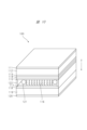
- FIG. 1 is a diagram illustrating an example of the configuration of a liquid crystal optical shutter according to a first embodiment.
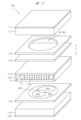
- 1 is a diagram showing the liquid crystal optical shutter according to the first embodiment disassembled into a plurality of parts;
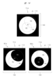
- FIG. 2 is a diagram showing the configuration of a light shielding layer and a second transparent electrode layer.
- 13A and 13B are diagrams for explaining the formation of a mask using a liquid crystal light shutter without misalignment of the light-shielding layer.
- 13A and 13B are diagrams for explaining the formation of a mask using a liquid crystal light shutter with a misaligned light-shielding layer.
- FIG. 11 is a diagram illustrating an example of the configuration of an imaging device according to a second embodiment.
- FIG. 11 is a diagram illustrating an example of the configuration of an arithmetic and control unit according to a second embodiment.
- FIG. 11 is a flowchart showing an example of the flow of operations of an imaging device according to a second embodiment.
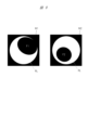
- FIG. 1 shows an example of two masks used in the DFD technique.
- 1A and 1B are diagrams illustrating schematic configurations of typical liquid crystal optical shutters.
- FIG. 1 is a diagram showing a generally conceivable liquid crystal light shutter disassembled into a plurality of parts.
- FIG. 2 is a diagram showing the configuration of a light shielding layer and a second transparent electrode layer.
- 13A and 13B are diagrams for explaining the formation of a mask using a liquid crystal light shutter.
- 11A and 11B are diagrams showing how the opening pattern of the mask changes due to misalignment of the light shielding layer.
- 1A to 1C are diagrams illustrating an example of a manufacturing method for a liquid crystal light shutter.
- the manner in which a subject is blurred in a captured image generally depends on the point spread function, which is determined by the optical system of the imaging device and the shape of the light entrance area of the optical system.
- the point spread function is determined for each mask. Imaging a subject with an imaging device equipped with a mask is called coded imaging.
- coded imaging When a subject is coded, a blurred image is obtained based on the point spread function specific to the mask used.
- FIG. 9 is a diagram showing examples of two masks used in DFD technology.
- Non-Patent Document 1 describes DFD technology using coded imaging with two masks.
- the black areas are areas that block light entering the optical system
- the white areas are areas of openings that allow light entering the optical system to pass through.
- the two masks M1 and M2 shown in FIG. 9 have different geometric patterns of openings (hereinafter also referred to as opening patterns) through which light can pass.
- Mask M1 is a mask in which an elliptical light-shielding region F1 is formed in the upper right corner of a circular light-entrance region RL.
- Mask M2 is a mask in which an elliptical light-shielding region F2 is formed in the lower left corner of the light-entrance region RL.
- the light entrance area RL may be the entire area where light enters the optical system of the imaging device from the subject, or may be an area narrower than that area.
- the light entrance area RL is generally defined by the user in relation to the optical system, but may also be determined based on other factors.
- the light entrance area RL is generally a circular area, but is not limited to this.
- one possible method for switching between multiple masks is to install a liquid crystal optical shutter in the light entrance area, which is the area where light enters the optical system.
- FIG. 10 is a schematic diagram showing an example of a typical liquid crystal optical shutter configuration.
- FIG. 11 is a diagram showing a typical liquid crystal optical shutter 100 disassembled into multiple parts. Note that the z direction in the diagram is the principal axis direction of the optical system of the imaging device.
- the liquid crystal light shutter 100 has a first polarizing plate 111, a first glass substrate 112, a light shielding layer 113, a first transparent electrode layer 114, a first alignment film 115, a liquid crystal layer 116, a second alignment film 117, a second transparent electrode layer 118, a second glass substrate 119, a second polarizing plate 120, a spacer 121, and a sealing layer 122.
- the liquid crystal optical shutter 100 forms the masks M1 and M2 shown in FIG. 9.
- an opening K1 of the same shape and size as the light entrance region RL of the optical system is formed in the light shielding layer 113, and four segment electrodes CR1 to CR4 corresponding to the divided regions obtained by dividing the light entrance region RL are formed in the second transparent electrode layer 118.
- FIG. 12 is a diagram showing the configuration of the light shielding layer 113 and the second transparent electrode layer 118.
- the light shielding layer 113 shields light in an area A1 other than the opening K1.
- the area of the opening K1 is, for example, a circular area with a diameter ⁇ 1.
- the light shielding layer 113 is made of, for example, a metal or resin, and has a black color that absorbs light.
- the segment electrodes CR1 to CR4 of the second transparent electrode layer 118 correspond to the segments R1 to R4 formed in the liquid crystal light shutter 100, respectively.
- a segment is an area in the liquid crystal layer 116 that can independently assume either a light blocking state or a light transmitting state by controlling the electrical signals applied to the segment electrodes CR1 to CR4 in the first transparent electrode layer 114 and the second transparent electrode layer 118.
- Segment R1 corresponds to the overlap region F3 between the light-shielding region F1 in the upper right corner of mask M1 and the light-shielding region F2 in the lower left corner of mask M2.
- Segment R2 corresponds to the region obtained by excluding overlap region F3 from light-shielding region F2.
- Segment R3 corresponds to the region obtained by excluding overlap region F3 from light-shielding region F1.
- Segment R4 corresponds to the region obtained by excluding light-shielding regions F1 and F2, i.e., segments R1 to R3, from the light entrance region RL.
- FIG. 13 is a diagram for explaining the formation of masks M1 and M2 using the liquid crystal optical shutter 100.
- a process is performed to apply the necessary electrical signals to the first transparent electrode layer 114 and each segment electrode so that segments R1 to R4 are in a light-transmitting state, as shown in state T11 in FIG. 13.
- a process is performed to apply the necessary electrical signals to the first transparent electrode layer 114 and each segment electrode so that segments R1 and R3 are in a light-shielding state and segments R2 and R4 are in a light-transmitting state, as shown in state T12 of FIG. 13.
- a process is performed to apply the necessary electrical signals to the first transparent electrode layer 114 and each segment electrode so that segments R1 and R2 are in a light-shielding state and segments R3 and R4 are in a light-transmitting state, as shown in state T13 of FIG. 13.
- the position and shape of the segment electrodes can be relatively accurately determined, but the position accuracy of the light-shielding layer tends to be relatively low. In other words, the alignment accuracy between the light-shielding layer and each segment electrode is likely to be low. If the alignment accuracy between the light-shielding layer and each segment electrode is low, the deviation between the actually formed mask aperture pattern and the intended aperture pattern cannot be ignored. Therefore, when decoding the captured image obtained by encoded imaging, the accuracy of estimating the depth of the subject decreases. The manner in which the mask aperture pattern deviates from the originally intended aperture pattern is explained with reference to the figure.
- Figure 14 shows how the mask opening pattern changes due to misalignment of the light shielding layer.
- the light-shielding layer 113 may erode part of the segment, or an area other than the segment may be formed that is always light-transmitting.
- a mask M1a different from mask M1 is formed.
- a mask M2a different from mask M2 is formed.
- FIG. 15 is a diagram showing an example of a manufacturing method for liquid crystal light shutters. It is assumed that the main manufacturing process for liquid crystal light shutters is carried out by a user operating a dedicated robot or device, but some of the manufacturing process may be carried out by the user himself.
- step H1 the light shielding layer 113 is bonded to the first glass substrate 112. Specifically, a work process is carried out in which the light shielding layer 113 is bonded to the first glass substrate 112 with an adhesive or the like.
- a transparent electrode layer is formed on the first glass substrate 112. Specifically, a transparent conductive film is vapor-deposited on the first glass substrate 112 to which the light-shielding layer 113 is attached, and a process is carried out to form the first transparent electrode layer 114, which serves as a common electrode.
- step H3 a transparent electrode layer is formed on the second glass substrate 119. Specifically, a process of depositing a transparent conductive film on the second glass substrate 119 is carried out.
- step H4 the electrode pattern is processed by photolithography. Specifically, a process is carried out in which a pattern of multiple segment electrodes is drawn by photolithography on the transparent conductive film deposited on the second glass substrate 119.
- the processing accuracy of electrode patterns by lithography is known to be very high, and it is said that it is possible to process within an error of about 1 ⁇ m.
- step H5 the alignment film is formed and the surface is treated. Specifically, a process is carried out in which a first alignment film 115 is formed on the first transparent electrode layer 114, and a second alignment film 117 is formed on the second transparent electrode layer 118. In addition, a process is carried out in which fine grooves are formed on the surfaces of the first alignment film 115 and the second alignment film 117 in order to align the liquid crystal molecules in a certain direction.
- step H6 the glass substrates are bonded together. Specifically, a work process is carried out in which a spacer 121 is sandwiched between the first glass substrate 112 and the second glass substrate 119, and the peripheral edge of the first glass substrate 112 and the peripheral edge of the second glass substrate 119 are fixed together with a sealing layer 122. These glass substrates can be bonded together with an error of about 1 ⁇ m to 5 ⁇ m.
- step H7 liquid crystal is injected and sealed. Specifically, the process of generating liquid crystal layer 116 is carried out by injecting liquid crystal between first glass substrate 112 and second glass substrate 119 and sealing the injection port.
- step H8 the polarizing plates are attached. Specifically, a work process is carried out in which the first polarizing plate 111 is attached to the outer side of the first glass substrate 112, i.e., the surface opposite the liquid crystal layer 116. In addition, a work process is carried out in which the second polarizing plate 120 is attached to the outer side of the second glass substrate 119, i.e., the surface opposite the liquid crystal layer 116.
- the second transparent electrode layer 118 is formed by depositing a transparent conductive film onto the second glass substrate 119 and processing the electrode pattern by lithography.
- Each segment is formed to correspond to the position and shape of each segment electrode in the second transparent electrode layer 118, so deviation from the intended position on the glass substrate can be suppressed to about 1 ⁇ m to 2 ⁇ m.
- the light-shielding layer 113 is adhered to the first glass substrate 112 using an adhesive or the like.
- the light-shielding layer 113 may be relatively largely displaced from the intended position on the first glass substrate 112 by about 5 ⁇ m to 10 ⁇ m. If the positional relationship between the light-shielding layer 113 and the first glass substrate 112 is displaced, a misalignment will occur in the positional relationship between the light-shielding layer 113 and the second transparent electrode layer 118 formed on the second glass substrate 119.
- the light shielding layer 113 may erode part of the light incidence region RL, and the opening pattern of the mask that is actually formed may deviate from the intended opening pattern to a non-negligible extent.
- encoded imaging is performed using a mask whose opening pattern is misaligned from the intended position, and the resulting captured image is decoded based on a point spread function that corresponds to the intended opening pattern, the depth accuracy of the subject will decrease.
- the liquid crystal light shutter according to embodiment 1 of the present application is a liquid crystal light shutter that forms a mask used for coding imaging, and includes a first transparent electrode layer, a second transparent electrode layer that is disposed opposite to the first transparent electrode layer and has a plurality of transparent segment electrodes, a liquid crystal layer that is disposed between the first transparent electrode layer and the second transparent electrode layer, and a light shielding layer that has an opening formed therein corresponding to an area that includes a light entrance area of an optical system used for coding imaging and is wider than the light entrance area, and that shields light in an outer area of the opening, the plurality of segment electrodes including an outer peripheral segment electrode that corresponds to an outer peripheral area of the light entrance area that includes the outline of the opening, and the mask is formed by controlling an electric signal applied to the first transparent electrode layer and each of the plurality of segment electrodes. Details of this liquid crystal light shutter are as follows.
- FIG. 1 is a schematic diagram showing an example of the configuration of a liquid crystal optical shutter according to embodiment 1.
- FIG. 2 is a diagram showing the liquid crystal optical shutter according to embodiment 1 disassembled into multiple parts. Note that the z direction in the diagram is the principal axis direction of the optical system of the imaging device.
- the liquid crystal light shutter 1 has a first polarizing plate 51, a first glass substrate 52, a light shielding layer 53, a first transparent electrode layer 54, a first alignment film 55, a liquid crystal layer 56, a second alignment film 57, a second transparent electrode layer 58, a second glass substrate 59, a second polarizing plate 60, a spacer 61, and a sealing layer 62.
- the liquid crystal light shutter 1 forms the masks M1 and M2 shown in FIG. 9.
- an opening K2 is formed in the light shielding layer 53, which corresponds to an area that includes the light entrance region RL of the optical system and is wider than the light entrance region RL.
- the opening K2 has a shape similar to the light entrance region RL, and is larger than the light entrance region RL by a width V.
- a total of five electrodes are formed on the second transparent electrode layer 58: four segment electrodes CR1 to CR4 and an outer peripheral segment electrode CR5.
- FIG. 3 is a diagram showing the configuration of the light shielding layer 53 and the second transparent electrode layer 58.
- the light shielding layer 53 shields light in the outer area A2 of the opening K2.
- the light incidence area RL is a circular area with a diameter of ⁇ 1
- the light shielding layer 53 is made of, for example, metal or resin, and has a black color that absorbs light.
- the segment electrodes CR1 to CR4 and the peripheral segment electrode CR5 in the second transparent electrode layer 58 correspond to the segments R1 to R4 and the peripheral segment R5 formed in the liquid crystal light shutter 1, respectively.
- Segments R1 to R4 are the same as segments R1 to R4 in the liquid crystal optical shutter 100 described above. That is, segment R1 is a segment corresponding to overlapping region F3 between light-shielding region F1 in the upper right of mask M1 and light-shielding region F2 in the lower left of mask M2. Segment R2 is a segment corresponding to the region obtained by excluding overlapping region F3 from light-shielding region F2. Segment R3 is a segment corresponding to the region obtained by excluding overlapping region F3 from light-shielding region F1. Segment R4 is a segment corresponding to the region obtained by excluding light-shielding regions F1 and F2, i.e., segments R1 to R3, from light entrance region RL.
- the peripheral segment R5 is a segment that corresponds to the combined region of segments R1 to R4, i.e., the peripheral region of the light entrance region RL.
- the peripheral segment R5 is a ring-shaped segment that is located adjacent to the outside of the light entrance region RL.
- Widths V and W are designed so that even if the light-shielding layer 53 is shifted from the intended position by the maximum expected deviation, the light-shielding layer 53 will not extend beyond the inner end of the outer peripheral segment R5.
- the width W of the band of the outer peripheral segment R5 is designed, for example, to be several to ten times the maximum expected deviation of the light-shielding layer 53. If the maximum expected deviation is, for example, 5 ⁇ m, then the width W is, for example, 10 ⁇ m to 30 ⁇ m, and the width V is, for example, W/2.
- the target position for placing the light-shielding layer 53 is, for example, a position where the inner end of the light-shielding layer 53 is as close as possible to the center of the band of the outer peripheral segment R5.
- widths V and W are merely examples and are not limited to these. However, the specific values in this embodiment are an example of realistic values when considering current manufacturing technology and the estimated amount of misalignment of the light shielding layer when manufacturing liquid crystal light shutters.
- Figure 4 is a diagram to explain the formation of a mask using a liquid crystal light shutter 1 with no misalignment of the light shielding layer.
- a process is performed to apply the necessary electrical signals to the first transparent electrode layer 54 and the electrodes corresponding to each segment so that segments R1, R3, and R5 are in a light-shielding state and segments R2 and R4 are in a light-transmitting state, as shown in state T2 in Figure 4.
- Figure 5 is a diagram to explain the formation of a mask using a liquid crystal light shutter 1 with a misaligned light shielding layer.
- the electrical signals applied to each electrode are controlled so that segments R1 to R4 are in a light-transmitting state and peripheral segment R5 is in a light-shielding state, as shown in state T4 in Figure 5.
- the light-shielding layer 53 is positioned at a position shifted from the intended position shown by the dashed line, the end of opening K2 in the light-shielding layer 53 is hidden by peripheral segment R5, which is in a light-shielding state, and does not encroach on the light incidence region RL, i.e., the region of segments R1 to R4. Therefore, it is possible to obtain a state in which no mask is formed and the opening is formed as intended.
- the electrical signals applied to each electrode are controlled so that segments R1, R3 and peripheral segment R5 are in a light-shielding state, and segments R2 and R4 are in a light-transmitting state, as shown in state T5 in Figure 5.
- the light-shielding layer 53 is positioned at a position shifted from the intended position, but the end of opening K2 in light-shielding layer 53 is hidden by peripheral segment R5 and does not encroach on the light incidence region RL, i.e., the region of segments R1 to R4. Therefore, it is possible to form a mask M1 with openings formed as intended.
- the electrical signals applied to each electrode are controlled so that segments R1, R2 and peripheral segment R5 are in a light-shielding state, and segments R3 and R4 are in a light-transmitting state, as shown in state T6 in FIG. 5.
- the light-shielding layer 53 is positioned at a position shifted from the intended position, but the end of opening K2 in light-shielding layer 53 is hidden by peripheral segment R5 and does not encroach on light incidence region RL, i.e., the region of segments R1 to R4. Therefore, it is possible to form mask M2 with openings formed as intended.
- the second transparent electrode layer 58 is formed by depositing a transparent conductive film onto the second glass substrate 59. Since each segment is formed to correspond to the shape of each electrode in the second transparent electrode layer 58, deviation from the intended position on the glass substrate can be suppressed to approximately 1 ⁇ m to 2 ⁇ m.
- the light-shielding layer 53 is bonded to the first glass substrate 52.
- the light-shielding layer 53 it is difficult to maintain high positional accuracy with respect to the glass substrate, and there is a possibility that the light-shielding layer 53 may be misaligned by several ⁇ m to 10 ⁇ m from the intended alignment position of the segments R1 to R4.
- the multiple segments include a ring-shaped peripheral segment R5 that is positioned outside the light incidence region RL. That is, a ring-shaped peripheral segment electrode CR5 that corresponds to the ring-shaped peripheral segment R5 is provided in the second transparent electrode layer 58. If the peripheral segment R5 is placed in a light-shielding state when the mask is formed, the inner end of the peripheral segment R5 is guaranteed to have high positional accuracy even if the light-shielding layer 53 is misaligned from the intended position.
- the opening pattern of the mask that is formed is not affected by the misalignment, and the difference from the intended opening pattern can be reduced.
- the first embodiment it is possible to provide a more practical DFD technology. More specifically, even if the light shielding layer 53 of the liquid crystal optical shutter 1 is arranged at a position shifted from the intended position due to the above-mentioned configuration, the position shift is absorbed by the presence of the peripheral segment R5. In other words, the opening pattern of the mask formed does not change. If the opening pattern of the mask does not change, the position shift of the light shielding layer 53 does not affect the decoding even if the captured image obtained by the coded imaging is decoded based on the point spread function corresponding to the originally intended mask opening pattern. Therefore, when decoding the captured image obtained by the coded imaging, it is possible to eliminate the decrease in the accuracy of subject depth estimation due to the position shift of the light shielding layer 53. This effect leads to improved practicality in the DFD technology.
- the liquid crystal light shutter 1 may have a configuration in which, among the multiple segment electrodes, two or more segment electrodes corresponding to segments that are commonly in a light-blocking state when multiple masks are formed include an outer peripheral segment electrode CR5 and are connected to each other.
- the liquid crystal optical shutter 1 is configured to connect an electrode corresponding to the ring-shaped peripheral segment R5 to an electrode corresponding to a segment that is always in a light-shielding state when forming a mask.
- the liquid crystal optical shutter 1 is configured to connect the peripheral segment electrode CR5 corresponding to the peripheral segment R5 and the segment electrode CR1 corresponding to segment R1 to each other.
- the electrodes of multiple segments that are in a light-blocking state can be combined into a single electrode, which not only simplifies the wiring of the electrodes but also reduces the wiring area that reduces transparency.
- the imaging device according to embodiment 2 is an imaging device that includes the liquid crystal optical shutter according to embodiment 1.
- FIG. 6 is a diagram showing an example of the configuration of an imaging device according to embodiment 2.
- the imaging device 2 according to embodiment 2 has an optical system section 20, an image sensor 30, a liquid crystal mask section 40, an optical system control section 21, an image sensor control section 31, a liquid crystal mask control section 41, and an arithmetic control section 10.
- the z direction in the figure is the principal axis direction of the optical system section 20.
- the optical system unit 20 collects light L, which is emitted or reflected light from the subject 4, and forms an image on the light receiving surface 30a of the image sensor 30 described below.
- the optical system unit 20 includes a lens 20a.
- the lens 20a is, for example, a fixed focus lens or a zoom lens.
- the lens 20a is generally a compound lens made up of multiple lenses, but may also be a single lens.
- the optical system unit 20 may be of an autofocus type or a fixed focus type.
- the image sensor 30 is an electronic component that performs photoelectric conversion.
- the image sensor 30 is a device that forms an image on the light receiving surface 30a of the image sensor 30 through the optical system unit 20, which receives light L that is emitted or reflected from the subject 4 that is a distance D (depth) away from the lens 20a, photoelectrically converts the brightness and darkness of the image into an amount of electric charge, and reads out and converts it into an electrical signal.
- the imaging element 30 generally has a plurality of photoelectric conversion elements arranged in a two-dimensional array, and these plurality of photoelectric conversion elements form a light receiving surface 30a.
- the imaging element 30 is positioned so that light L that enters the optical system unit 20 from the subject 4 and passes through the optical system unit 20 is received by the light receiving surface 30a.
- the imaging element 30 converts the intensity of the light received by the light receiving surface 30a, i.e., brightness, into an electrical signal and outputs an image signal.
- the imaging element 30 may be one that outputs a color image signal representing a color image, or one that outputs a monochrome image signal representing a monochrome image.
- the imaging element 30 is, for example, a CCD (Charge Coupled Devices) image sensor or a COMS (Complementary Metal Oxide Semiconductor) image sensor.
- CCD Charge Coupled Devices
- COMS Complementary Metal Oxide Semiconductor
- the liquid crystal mask unit 40 is provided in front of the optical system unit 20 on the subject 4 side.
- the liquid crystal mask unit 40 has the function of making one of a number of predetermined masks appear, or making none of the masks appear.
- the liquid crystal mask unit 40 may be provided inside the optical system unit 20.
- the liquid crystal mask section 40 is configured so that it can be placed in a state where either the mask M1 or M2 is installed on the subject 4 side of the optical system section 20, or in a state where there is no mask.
- the liquid crystal mask section 40 has the liquid crystal optical shutter 1 described above.
- the optical system control unit 21 adjusts the position of the movable parts included in the optical system unit 20 based on a control signal received from the calculation control unit 10.
- the optical system control unit 21 has, for example, a drive motor, and moves at least a part of the lens by operating the drive motor.
- the optical system control unit 21 may change the zoom magnification by moving some of the lenses that make up the zoom lens, or adjust the focus by moving the entire zoom lens. If the optical system unit 20 includes a fixed focal length lens, the focus may be adjusted by moving the entire lens. If the optical system unit 20 includes an aperture mechanism, the aperture opening diameter may be adjusted by operating the aperture mechanism.
- the imaging device control unit 31 performs imaging by reading the image signal output from the imaging device 30 based on the control signal received from the calculation control unit 10.
- the imaging device control unit 31 transmits the read image signal to the calculation control unit 10.
- the shutter method used to control the imaging device 30 to capture an image of the subject 4 may be, for example, a global shutter method or a rolling shutter method.
- the liquid crystal mask control unit 41 controls the liquid crystal mask unit 40 based on the control signal received from the calculation control unit 10, and realizes a state in which the intended mask M is installed in the liquid crystal mask unit 40, or a state in which the mask M is not installed.
- ⁇ Configuration example of the arithmetic control unit> 7 is a diagram showing an example of the configuration of the arithmetic and control unit 10 according to embodiment 2.
- the arithmetic and control unit 10 is, for example, a computer, and has a processor 11, a memory 12, and an interface 13.
- Memory 12 stores programs P that are used by processor 11 to execute various types of arithmetic processing or image processing, and to execute various types of control processing. Memory 12 also temporarily or long-term stores data that processor 11 processes.
- Processor 11 reads and executes program P stored in memory 12 to execute various processes including arithmetic processing, image processing, and control processing. When executing various processes, processor 11 stores data in memory 12 and accesses data stored in memory 12 to execute the processes.
- the processor 11 executes unmasked imaging process, representative edge direction determination process, mask selection process, first mask imaging process, second mask imaging process, decoding process, subject depth estimation process, depth map generation process, data output process, and imaging continuation determination process. Details of these various processes will be described later.
- the processor 11 transmits control signals to the optical system control unit 21, the image sensor control unit 31, and the liquid crystal mask control unit 41 to execute the above-mentioned maskless imaging process, representative edge direction determination process, mask selection process, first mask imaging process, and second mask imaging process.
- the interface 13 is connected to the external device 3 and transmits the decoded image or depth map DM generated in the calculation control unit 10 to the external device 3.
- all or part of the above computer may be composed of semiconductor circuits such as a DSP (Digital Signal Processor), ASIC (Application Specific Integrated Circuit), FPGA (Field Programmable Gate Array), or CPLD (Complex Programmable Logic Device).
- DSP Digital Signal Processor
- ASIC Application Specific Integrated Circuit
- FPGA Field Programmable Gate Array
- CPLD Complex Programmable Logic Device
- the external device 3 is, for example, an image processing device, a vehicle driving assistance device, etc.
- the image processing device processes the captured image, for example, by blurring the background that is far from the optical system and emphasizing the subject that is attracting attention.
- the vehicle driving assistance device detects, for example, the positions or relative moving speed of objects around the vehicle, and issues warnings or controls the vehicle to avoid danger.
- the operation unit 17 and the display unit 18 are connected to the calculation control unit 10.
- the operation unit 17 is for receiving input operations from the user, and the display unit 18 is for visually outputting information for the user.
- the operation unit 17 is, for example, a keyboard, a mouse, a button, a dial, etc.
- the display unit 18 is, for example, a liquid crystal panel, an organic EL panel, etc.
- the operation unit 17 and the display unit 18 may be an integrated touch panel.
- the operation unit 17 and the display unit 18 may be provided on the external device 3 side.
- FIG. 8 is a flow diagram showing an example of the flow of operations of the imaging device 2 according to the second embodiment.
- step S1 the first mask M1 is formed.
- the calculation control unit 10 sends a control signal to the liquid crystal mask control unit 41 so that mask M1 is formed on the liquid crystal light shutter 1.
- the liquid crystal mask control unit 41 applies the necessary electrical signals to each electrode of the liquid crystal light shutter 1, and controls the state of each segment to a light-transmitting state or a light-blocking state, thereby creating a state in which mask M1 is formed.
- step S2 encoded imaging of the subject is performed using the first mask.
- the calculation control unit 10 transmits a control signal to the image sensor control unit 31 so that the subject 4 is encoded and imaged using the formed mask M1.
- the image sensor control unit 31 controls the image sensor 30 so that the subject 4 is imaged, i.e., so that an imaged image P1 of the subject 4 represented by the output signal of the image sensor 30 is transmitted to the calculation control unit 10.
- step S3 the second mask M2 is formed.
- the calculation control unit 10 sends a control signal to the liquid crystal mask control unit 41 so that mask M2 is formed on the liquid crystal light shutter 1.
- the liquid crystal mask control unit 41 applies the necessary electrical signals to each electrode of the liquid crystal light shutter 1, and controls the state of each segment to a light-transmitting state or a light-blocking state, thereby creating a state in which mask M2 is formed.
- step S4 encoded imaging of the subject is performed using the second mask.
- the calculation control unit 10 transmits a control signal to the image sensor control unit 31 so that the subject 4 is encoded and imaged using the formed mask M2.
- the image sensor control unit 31 controls the image sensor 30 so that the subject 4 is imaged, i.e., so that an imaged image P2 of the subject 4 represented by the output signal of the image sensor 30 is transmitted to the calculation control unit 10.
- step S5 the captured images are decoded. Specifically, the calculation control unit 10 decodes the captured images P1 and P2 obtained based on the point spread function corresponding to mask M1 and the point spread function corresponding to mask M2.
- step S6 a decoded image and subject depth information are obtained.
- the calculation control unit 10 obtains a decoded image of the subject 4 and depth estimation information of objects corresponding to each position in the decoded image based on the information obtained by the above decoding.
- step S7 a depth map is generated. Specifically, the calculation control unit 10 generates a depth map DM of the subject 4 based on the obtained decoded image and the depth estimation information.
- step S8 the depth map is output. Specifically, the calculation control unit 10 outputs the generated depth map DM to the external device 3.
- the imaging device 2 the formation of a mask used for encoding imaging is realized by the liquid crystal optical shutter 1.
- the liquid crystal optical shutter 1 can realize any mask depending on the design of the segments, and there is no need to physically switch hardware to switch the state of the mask. Therefore, the position of the mask can be controlled with high precision, and the mechanism for switching the mask can also be simplified.
- the present invention is not limited to the above-mentioned embodiments and includes various modified examples. Furthermore, the above-mentioned embodiments have been described in detail to clearly explain the present invention, and are not necessarily limited to those having all of the configurations described. Furthermore, it is possible to replace part of the configuration of one embodiment with the configuration of another embodiment, and it is also possible to add the configuration of another embodiment to the configuration of one embodiment. All of these belong to the scope of the present invention. Furthermore, the numerical values etc. contained in the text and figures are merely examples, and the effect of the present invention will not be impaired if different ones are used.
- 1...liquid crystal optical shutter 2...imaging device, 3...external device, 4...subject, 10...arithmetic control unit, 11...processor, 12...memory, 13...interface, 17...operation unit, 18...display unit, 20...optical system unit, 21...optical system control unit, 30...imaging element, 31...imaging element control unit, 40...liquid crystal mask unit, 41...liquid crystal mask control unit, 51...first polarizing plate, 52...first glass substrate, 53...light shielding layer, 54...first transparent electrode layer, 55...first alignment film, 56...liquid crystal layer, 57...second alignment film , 58...second transparent electrode layer, 59...second glass substrate, 60...second polarizing plate, 61...spacer, 62...sealing layer, A2...outer region, CR1-CR4...segment electrodes, CR5...peripheral segment electrode, D...depth, K2...opening, L...light, M1, M2, M1a, M2a...mask, P...pro
Landscapes
- Physics & Mathematics (AREA)
- Nonlinear Science (AREA)
- General Physics & Mathematics (AREA)
- Chemical & Material Sciences (AREA)
- Crystallography & Structural Chemistry (AREA)
- Optics & Photonics (AREA)
- Mathematical Physics (AREA)
- Geometry (AREA)
- Engineering & Computer Science (AREA)
- Multimedia (AREA)
- Signal Processing (AREA)
- Liquid Crystal (AREA)
- Diaphragms For Cameras (AREA)
- Studio Devices (AREA)
Abstract
符号化撮像による被写体奥行き推定において、実用性を向上させる。 第1の透明電極層と、第1の透明電極層に対向して配置され、複数の透明なセグメント電極を有する第2の透明電極層58と、第1の透明電極層と第2の透明電極層58との間に配置される液晶層と、符号化撮像に用いる光学系の光入射領域RLを含み光入射領域RLよりも広い領域に対応した開口K2が形成され、開口K2の外側領域において光を遮蔽する光遮蔽層53と、を備え、複数のセグメント電極は、開口K2の輪郭が含まれる光入射領域RLの外周領域に対応した外周セグメント電極CR5を含み、第1の透明電極層と複数のセグメント電極の各々とに印加される電気信号が制御されることによりマスクが形成される、液晶光シャッタ1を提供する。
Description
本発明は、液晶光シャッタおよび撮像装置に関する。
符号化撮像の分野において、DFD(Depth From Defocus)と呼ばれる技術が知られている。DFD技術は、撮像により得られた画像に写り込んでいるエッジのボケ具合を基に、撮像装置の光学系から被写体までの距離、すなわち被写体の深度あるいは奥行きを推定する技術である。
DFD技術は、例えば、非特許文献1に記載されている。非特許文献1に記載のDFD技術では、光が通過する開口の位置が互いに異なる2つのマスクが用意される。次に、2つのマスクのそれぞれについて、マスクを光学系の光入射領域に配置して同一の被写体を撮像する符号化撮像が行われる。次いで、符号化撮像により得られた2つの撮像画像に、それぞれのマスクに固有の点拡がり関数に基づく復号化処理が施され、被写体の奥行きが推定される。なお、点拡がり関数は、一般的に、PSF(Point Spread Function)と呼ばれており、ボケ関数、ボケ広がり関数、点像分布関数などとも言われる。
"Coded Aperture Pairs for Depth from Defocus and Defocus Deblurring" C. Zhou, S. Lin and S.K. Nayar, International Journal of Computer Vision, Vol. 93, No. 1, pp. 53, May. 2011.
DFD技術は、未だ発展途上にあり、DFD技術には、実用性において向上の余地が多く残されている。上記事情により、より実用性の高いDFD技術が望まれている。
本願において開示される発明のうち、代表的なものの概要を説明すれば、次の通りである。
本願発明の代表的な一実施形態は、符号化撮像に用いられるマスクを形成する液晶光シャッタであって、第1の透明電極層と、前記第1の透明電極層に対向して配置され、複数の透明なセグメント電極を有する第2の透明電極層と、前記第1の透明電極層と前記第2の透明電極層との間に配置される液晶層と、前記符号化撮像に用いる光学系の光入射領域を含み前記光入射領域よりも広い領域に対応した開口が形成され、前記開口の外側領域において光を遮蔽する光遮蔽層と、を備え、前記複数のセグメント電極は、前記開口の輪郭が含まれる前記光入射領域の外周領域に対応した外周セグメント電極を含み、前記第1の透明電極層と前記複数のセグメント電極の各々とに印加される電気信号が制御されることにより前記マスクが形成される、液晶光シャッタである。
本願発明の代表的な一実施形態は、前記液晶光シャッタを備える撮像装置である。
本願発明の各実施形態を説明する前に、本願発明に関するDFD技術について説明する。
撮像画像における被写体のボケの態様は、一般的に、撮像装置の光学系、光学系の光入射領域の形状などによって定まる点拡がり関数に依存する。光学系の光入射領域に、光を部分的に遮蔽するマスクが設置された場合、点拡がり関数は、マスク別に定まる。マスクが設置された撮像装置で被写体を撮像することは、符号化撮像と呼ばれる。被写体を符号化撮像すると、使用したマスクに固有の点拡がり関数に基づいてボケた画像が取得される。
このボケた画像に対して、使用したマスクに固有の点拡がり関数に基づく逆畳み込みをする復号化処理が施されると、ボケが改善された復号化画像と、復号化画像の各位置に対応する物体の奥行き情報とが得られる。
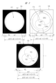
図9は、DFD技術に用いられる2つのマスクの例を示す図である。非特許文献1には、2つのマスクを用いた符号化撮像によるDFD技術が記載されている。図9に示す2つのマスクM1,M2において、黒い領域は光学系に入射する光を遮蔽する領域であり、白い領域は光学系に入射する光を通過させる開口の領域である。このように、図9に示す2つのマスクM1,M2は、光が通過し得る開口の幾何学的パターン(以下、開口パターンともいう。)が互いに異なっている。
マスクM1は、円形である光入射領域RLの右上に楕円形である光遮蔽領域F1が形成されたマスクである。また、マスクM2は、光入射領域RLの左下に楕円形である光遮蔽領域F2が形成されたマスクである。
なお、本明細書において、光入射領域RLは、被写体から撮像装置の光学系に光入射するすべての領域であってもよいし、当該領域より狭い領域であってもよい。光入射領域RLは、一般的には、光学系との関係でユーザにより規定されることが多いが、他の要素に基づいて決定されてもよい。また、光入射領域RLは、円領域が一般的であるが、これに限定されるものではない。
開口パターンが異なる複数のマスクを用いた符号化撮像によるDFD技術において、複数のマスクを切り替えて形成する手法の一つとして、光学系へ光が入射する領域である光入射領域に液晶光シャッタを設置する手法が考えられる。
図10は、一般的に考えられる液晶光シャッタの構成例を概略的に示す図である。また、図11は、一般的に考えられる液晶光シャッタ100を複数の部分に分解して示す図である。なお、図中のz方向は、撮像装置の光学系の主軸方向である。
図10および図11に示すように、液晶光シャッタ100は、第1の偏光板111、第1のガラス基板112、光遮蔽層113、第1の透明電極層114、第1の配向膜115、液晶層116、第2の配向膜117、第2の透明電極層118、第2のガラス基板119、第2の偏光板120、スペーサ121、およびシール層122を有している。
ここで、液晶光シャッタ100は、図9に示すマスクM1,M2を形成するものとする。これらのマスクM1,M2を形成できるようにするために、光遮蔽層113には、光学系の光入射領域RLと同じ形状および大きさの開口K1が形成されており、第2の透明電極層118には、光入射領域RLを分割した分割領域に対応する4つのセグメント電極CR1~CR4が形成されている。
図12は、光遮蔽層113および第2の透明電極層118の構成を示す図である。図12に示すように、光遮蔽層113は、開口K1以外の領域A1において光を遮蔽する。開口K1の領域は、例えば直径φ1の円領域である。光遮蔽層113は、例えば、金属あるいは樹脂で構成されており、光を吸収する黒色を有している。
図12に示すように、第2の透明電極層118のセグメント電極CR1~CR4は、液晶光シャッタ100において形成されるセグメントR1~R4とそれぞれ対応している。セグメントとは、液晶層116において、第1の透明電極層114と第2の透明電極層118における各セグメント電極CR1~CR4とに印加する電気信号を制御することにより、光遮蔽状態と光透過状態のいずれかの状態を独立して取ることができる領域である。
セグメントR1は、マスクM1の右上の光遮蔽領域F1と、マスクM2の左下の光遮蔽領域F2との重複領域F3に対応したセグメントである。セグメントR2は、光遮蔽領域F2から重複領域F3を除いた領域に対応したセグメントである。セグメントR3は、光遮蔽領域F1から重複領域F3を除いた領域に対応したセグメントである。セグメントR4は、光入射領域RLから光遮蔽領域F1,F2すなわちセグメントR1~R3の領域を除いた領域に対応したセグメントである。
図13は、液晶光シャッタ100を用いたマスクM1,M2の形成を説明するための図である。マスクを形成しない場合、図13の状態T11に示すように、セグメントR1~R4が光透過状態となるように、第1の透明電極層114と各セグメント電極とに必要な電気信号を印加する処理が実行される。
マスクM1を形成する場合、図13の状態T12に示すように、セグメントR1,R3が光遮蔽状態となり、セグメントR2,R4が光透過状態となるように、第1の透明電極層114と各セグメント電極とに必要な電気信号を印加する処理が実行される。また、マスクM2を形成する場合、図13の状態T13に示すように、セグメントR1,R2が光遮蔽状態となり、セグメントR3,R4が光透過状態となるように、第1の透明電極層114と各セグメント電極とに必要な電気信号を印加する処理が実行される。
一方、本発明者らは、上記の如くマスクの形成に液晶光シャッタを用いた場合に、次に説明する課題があることを見出した。
液晶光シャッタでは、現在の製造技術の特性上、セグメント電極の位置および形状の精度は比較的高くできるが、光遮蔽層の位置の精度は比較的低くなる傾向がある。すなわち、光遮蔽層と各セグメント電極との位置合わせ精度が低くなりやすい。光遮蔽層と各セグメント電極との位置合わせ精度が低いと、実際に形成されるマスクの開口パターンと意図した開口パターンとのずれが無視できなくなる。故に、符号化撮像により得られる撮像画像を復号化する際に、被写体の奥行き推定精度が低くなる。マスクの開口パターンが本来意図した開口パターンからずれる様子を、図を参照して説明する。
図14は、光遮蔽層の位置ずれによりマスクの開口パターンが変化する様子を示す図である。
図14の状態T14に示すように、光遮蔽層113が、破線で示す本来意図した位置からずれた場合、例えば、光遮蔽層113がセグメントの一部を侵食したり、セグメント以外の領域において常に光透過状態となる領域が形成されたりする。
そのため、例えば、図14の状態T15に示すように、マスクM1を形成しようとして、セグメントR1,R3が光遮蔽状態となり、セグメントR2,R4が光透過状態となるようにしても、マスクM1とは異なるマスクM1aが形成される。同様に、例えば、図14の状態T16に示すように、マスクM2を形成しようとして、セグメントR1,R2が光遮蔽状態となり、セグメントR3,R4が光透過状態となるようにしても、マスクM2とは異なるマスクM2aが形成される。
上記課題が生じる原因は、液晶光シャッタすなわち液晶パネルの一般的な製造方法を知ることで、より理解し易くなる。そこで、以下に、液晶光シャッタの製造方法として一般的に考えられる方法の一例について説明する。
図15は、液晶光シャッタの製造方法の一例を示す図である。なお、想定では、液晶光シャッタの主要な製造工程は、専用のロボットあるいは装置をユーザが操作することにより実施されるが、製造工程の一部は、ユーザ自身により実施されてもよい。
図15に示すように、まず、ステップH1において、第1のガラス基板112への光遮蔽層113の接着が行われる。具体的には、第1のガラス基板112に光遮蔽層113を接着剤等により接着する作業工程が実施される。
次に、ステップH2において、第1のガラス基板112への透明電極層の形成が行われる。具体的には、光遮蔽層113が接着された第1のガラス基板112に透明導電膜を蒸着し、コモン電極となる第1の透明電極層114を形成する作業工程が実施される。
次いで、ステップH3において、第2のガラス基板119への透明電極層の形成が行われる。具体的には、第2のガラス基板119に透明導電膜を蒸着する作業工程が実施される。
次いで、ステップH4において、フォトリソグラフィによる電極パターンの加工が行われる。具体的には、第2のガラス基板119に蒸着された透明導電膜に対し、フォトリソグラフィによって、複数のセグメント電極のパターンを描く作業工程が実施される。なお、リソグラフィによる電極パターンの加工精度は、非常に高いことが知られており、1μm程度の誤差内で加工することが可能であると言われている。
次いで、ステップH5において、配向膜の形成および表面処理が行われる。具体的には、第1の透明電極層114の上から第1の配向膜115を形成し、第2の透明電極層118の上から第2の配向膜117を形成する作業工程が実施される。また、第1の配向膜115および第2の配向膜117の表面には、液晶分子を一定方向に並べるための細かい溝を形成する作業工程が実施される。
次いで、ステップH6において、ガラス基板同士の貼合せが行われる。具体的には、第1のガラス基板112と第2のガラス基板119との間にスペーサ121を挟み込み、第1のガラス基板112の周縁部と第2のガラス基板119の周縁部とをシール層122で固定する作業工程が実施される。これらガラス基板同士は、1μm~5μm程度の誤差で貼り合わすことが可能である。
次いで、ステップH7において、液晶の注入および封止が行われる。具体的には、第1のガラス基板112と第2のガラス基板119との間に液晶を注入し、注入口を封止することにより、液晶層116を生成する作業工程が実施される。
次いで、ステップH8において、偏光板の貼付けが行われる。具体的には、第1のガラス基板112の外側すなわち液晶層116とは反対側の面に第1の偏光板111を貼り付ける作業工程が実施される。また、第2のガラス基板119の外側すなわち液晶層116とは反対側の面に第2の偏光板120を貼り付ける作業工程が実施される。
上述の通り、第2の透明電極層118は、第2のガラス基板119に透明導電膜を蒸着し、リソグラフィで電極のパターンを加工することにより形成される。各セグメントは、第2の透明電極層118における各セグメント電極の位置および形状に対応して形成されるため、ガラス基板における意図した位置からのずれを1μm~2μm程度に抑えることができる。
一方、光遮蔽層113は、第1のガラス基板112に接着剤等を用いて接着される。この場合、光遮蔽層113は、第1のガラス基板112において、意図した位置からのずれが5μm~10μm程度と比較的大きくなり得る。光遮蔽層113と第1のガラス基板112の位置関係がずれると、光遮蔽層113と第2のガラス基板119に形成されている第2の透明電極層118との位置関係にズレが生じる。
光遮蔽層113の位置ずれが大きいと、光入射領域RLの一部を侵食し、実際に形成されるマスクの開口パターンが、意図した開口パターンから無視できない程度にずれる可能性がある。その結果、開口パターンが意図した位置からずれたマスクを用いて符号化撮像を行い、得られた撮像画像に対して、意図した開口パターンに対応した点拡がり関数に基づく復号化を行うと、被写体の奥行き精度が低下する。
上記事情により、符号化撮像用のマスクを形成する液晶光シャッタにおいて、形成されるマスクの開口パターンと意図した開口パターンとのずれを低減することができる技術が望まれている。
本発明者らは、上記事情に鑑み、鋭意検討の結果、本願発明を考案した。以下に、本願発明の各実施形態について説明する。なお、以下で説明する各実施形態は、本願発明を実施するための一例であり、本願発明の技術的範囲を限定するものではない。また、以下の各実施形態において、同一の機能を有する構成要素には同一の符号を付し、その繰り返しの説明は、特に必要な場合を除き省略する。
(実施形態1)
本願の実施形態1に係る液晶光シャッタについて説明する。本願の実施形態1に係る液晶光シャッタは、符号化撮像に用いられるマスクを形成する液晶光シャッタであって、第1の透明電極層と、第1の透明電極層に対向して配置され、複数の透明なセグメント電極を有する第2の透明電極層と、第1の透明電極層と第2の透明電極層との間に配置される液晶層と、符号化撮像に用いる光学系の光入射領域を含み光入射領域よりも広い領域に対応した開口が形成され、開口の外側領域において光を遮蔽する光遮蔽層と、を備え、複数のセグメント電極は、開口の輪郭が含まれる光入射領域の外周領域に対応した外周セグメント電極を含み、第1の透明電極層と複数のセグメント電極の各々とに印加される電気信号が制御されることによりマスクが形成される、液晶光シャッタである。本液晶光シャッタの詳細は、下記の通りである。
本願の実施形態1に係る液晶光シャッタについて説明する。本願の実施形態1に係る液晶光シャッタは、符号化撮像に用いられるマスクを形成する液晶光シャッタであって、第1の透明電極層と、第1の透明電極層に対向して配置され、複数の透明なセグメント電極を有する第2の透明電極層と、第1の透明電極層と第2の透明電極層との間に配置される液晶層と、符号化撮像に用いる光学系の光入射領域を含み光入射領域よりも広い領域に対応した開口が形成され、開口の外側領域において光を遮蔽する光遮蔽層と、を備え、複数のセグメント電極は、開口の輪郭が含まれる光入射領域の外周領域に対応した外周セグメント電極を含み、第1の透明電極層と複数のセグメント電極の各々とに印加される電気信号が制御されることによりマスクが形成される、液晶光シャッタである。本液晶光シャッタの詳細は、下記の通りである。
図1は、実施形態1に係る液晶光シャッタの構成例を概略的に示す図である。また、図2は、実施形態1に係る液晶光シャッタを複数の部分に分解して示す図である。なお、図中のz方向は、撮像装置の光学系の主軸方向である。
図1および図2に示すように、液晶光シャッタ1は、第1の偏光板51、第1のガラス基板52、光遮蔽層53、第1の透明電極層54、第1の配向膜55、液晶層56、第2の配向膜57、第2の透明電極層58、第2のガラス基板59、第2の偏光板60、スペーサ61、およびシール層62を有している。
ここで、液晶光シャッタ1は、図9に示すマスクM1,M2を形成するものとする。これらのマスクM1,M2を形成できるようにするために、光遮蔽層53には、光学系の光入射領域RLを含み光入射領域RLより広い領域に対応した開口K2が形成されている。本実施例では、開口K2は、光入射領域RLと相似な形状を有し、光入射領域RLより幅Vだけ外側に広がった大きさを有している。また、第2の透明電極層58には、4つのセグメント電極CR1~CR4および外周セグメント電極CR5の計5つの電極が形成されている。
図3は、光遮蔽層53および第2の透明電極層58の構成を示す図である。図3に示すように、光遮蔽層53は、開口K2の外側領域A2において光を遮蔽する。本実施例では、光入射領域RLは直径φ1の円領域であり、開口K2の領域は、例えば、直径φ2(=φ1+2×V)の円領域である。光遮蔽層53は、例えば、金属あるいは樹脂で構成されており、光を吸収する黒色を有している。
図3に示すように、第2の透明電極層58におけるセグメント電極CR1~CR4および外周セグメント電極CR5は、液晶光シャッタ1において形成されるセグメントR1~R4および外周セグメントR5とそれぞれ対応している。
セグメントR1~R4は、先述した液晶光シャッタ100におけるセグメントR1~R4と同様である。すなわち、セグメントR1は、マスクM1の右上の光遮蔽領域F1と、マスクM2の左下の光遮蔽領域F2との重複領域F3に対応したセグメントである。セグメントR2は、光遮蔽領域F2から重複領域F3を除いた領域に対応したセグメントである。セグメントR3は、光遮蔽領域F1から重複領域F3を除いた領域に対応したセグメントである。セグメントR4は、光入射領域RLから光遮蔽領域F1,F2すなわちセグメントR1~R3の領域を除いた領域に対応したセグメントである。
外周セグメントR5は、セグメントR1~R4を合わせた領域すなわち光入射領域RLの外周領域に対応したセグメントである。本実施例では、外周セグメントR5は、光入射領域RLの外側に隣接して配置される環形状のセグメントである。外周セグメントR5の帯の幅はWである。すなわち、外周セグメントR5の内側端部を形成する円の直径はφ1であり、外周セグメントR5の外側端部を形成する円の直径はφ3(=φ1+2×W)である。
幅Vおよび幅Wは、光遮蔽層53が意図した位置から、想定される最大ずれ量だけずれた場合であっても、光遮蔽層53が外周セグメントR5の内側端部からはみ出ないように設計される。外周セグメントR5の帯の幅Wは、例えば、光遮蔽層53の想定される最大ずれ量の数倍~十数倍程度に設計される。想定される最大ずれ量が、例えば5μmであれば、幅Wは、例えば10μm~30μm、幅Vは例えばW/2である。光遮蔽層53を配置する際の目標位置は、例えば、光遮蔽層53の内側端部が、外周セグメントR5の帯の中央に極力近づくような位置である。
なお、幅V,Wの具体的な値はあくまで一例であり、これに限定されるものではない。ただし、本実施例での具体的な値は、液晶光シャッタを製造する上で、現在の製造技術、光遮蔽層の位置ずれ見積もり量等に鑑みると、現実的な値の一例である。
ここで、液晶光シャッタ1によるマスクの形成について説明する。まず、光遮蔽層53が意図した位置に配置されている場合について考える。
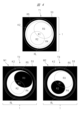
図4は、光遮蔽層の位置ずれがない液晶光シャッタ1によるマスクの形成を説明するための図である。
マスクを形成しない場合、セグメントR1~R4が光透過状態となり、外周セグメントR5が光遮蔽状態となるように、第1の透明電極層54と各セグメントに対応する電極とに必要な電気信号を印加する処理が実行される。
マスクM1を形成する場合、図4の状態T2に示すように、セグメントR1,R3,R5が光遮蔽状態となり、セグメントR2,R4が光透過状態となるように、第1の透明電極層54と各セグメントに対応する電極とに必要な電気信号を印加する処理が実行される。
また、マスクM2を形成する場合、図4の状態T3に示すように、セグメントR1,R2,R5が光遮蔽状態となり、セグメントR3,R4が光透過状態となるように、第1の透明電極層54と各セグメントに対応する電極とに必要な電気信号を印加する処理が実行される。
次に、光遮蔽層53が意図した位置からずれた位置に配置されている場合について考える。
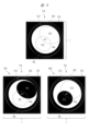
図5は、光遮蔽層の位置ずれがある液晶光シャッタ1によるマスクの形成を説明するための図である。
マスクを形成しない場合、光遮蔽層53の位置ずれがない場合と同様、図5の状態T4に示すように、セグメントR1~R4が光透過状態となり、外周セグメントR5が光遮蔽状態となるように、各電極に印加される電気信号が制御される。光遮蔽層53は破線で示す意図した位置からずれた位置に配置されているが、光遮蔽層53の開口K2の端部は、光遮蔽状態である外周セグメントR5に隠れ、光入射領域RLすなわちセグメントR1~R4の領域を侵食しない。したがって、意図した通りの開口が形成された、マスクを形成しない状態を得ることができる。
マスクM1を形成する場合、光遮蔽層53の位置ずれがない場合と同様、図5の状態T5に示すように、セグメントR1,R3,外周セグメントR5が光遮蔽状態となり、セグメントR2,R4が光透過状態となるように、各電極に印加される電気信号が制御される。この場合も、光遮蔽層53は意図した位置からずれた位置に配置されているが、光遮蔽層53の開口K2の端部は、外周セグメントR5に隠れ、光入射領域RLすなわちセグメントR1~R4の領域を侵食しない。したがって、意図した通りの開口が形成された、マスクM1を形成することができる。
また、マスクM2を形成する場合、光遮蔽層53の位置ずれがない場合と同様、図5の状態T6に示すように、セグメントR1,R2,外周セグメントR5が光遮蔽状態となり、セグメントR3,R4が光透過状態となるように、各電極に印加される電気信号が制御される。この場合も、光遮蔽層53は意図した位置からずれた位置に配置されているが、光遮蔽層53の開口K2の端部は、外周セグメントR5に隠れ、光入射領域RLすなわちセグメントR1~R4の領域を侵食しない。したがって、意図した通りの開口が形成された、マスクM2を形成することができる。
上述の通り、第2の透明電極層58は、第2のガラス基板59に透明導電膜を蒸着することにより形成される。各セグメントは、第2の透明電極層58における各電極形状に対応して形成されるため、ガラス基板における意図した位置からのずれを1μm~2μm程度に抑えることができる。
一方、光遮蔽層53は、第1のガラス基板52に接着される。光遮蔽層53は接着される場合、ガラス基板に対して高い位置精度を持つことが困難であり、光遮蔽層53とセグメントR1~R4との意図した合わせ位置から数μm~10μmのずれが生じる可能性がある。
しかしながら、本実施形態では、複数のセグメントの中に、光入射領域RLに対応したセグメントR1~R4に加え、光入射領域RLの外側に配置される環形状の外周セグメントR5が含まれている。すなわち、第2の透明電極層58の中に、当該環形状の外周セグメントR5に対応する環形状の外周セグメント電極CR5が設けられている。マスクを形成する際に、外周セグメントR5の状態を光遮蔽状態にすれば、光遮蔽層53が意図した位置からずれていたとしても、外周セグメントR5の内側端部は、高い位置精度が担保される。
したがって、光遮蔽層53に比較的大きな位置ずれが生じたとしても、形成されるマスクの開口パターンは、その位置ずれの影響を受けず、意図した開口パターンとの差異を小さくすることができる。
このような実施形態1によれば、より実用性の高いDFD技術を提供することができる。より詳しくは、液晶光シャッタ1は、上記構成により、光遮蔽層53が意図した位置からずれて配置されても、その位置ずれは外周セグメントR5の存在により吸収される。すなわち、形成されるマスクの開口パターンは変化しない。マスクの開口パターンが変化しないのであれば、符号化撮像によって得られた撮像画像に対して本来意図したマスクの開口パターンに対応した点拡がり関数に基づく復号化を行っても、光遮蔽層53の位置ずれは復号化に影響しない。故に、符号化撮像により得られる撮像画像を復号化する際に、光遮蔽層53の位置ずれに基づく被写体の奥行き推定精度の低下を排除することができる。そして、当該効果は、DFD技術において実用性を向上させることにつながる。
〈変形例〉
液晶光シャッタ1は、複数のセグメント電極のうち、複数のマスクを形成する場合に共通して光遮蔽状態となるセグメントに対応する2以上のセグメント電極が、外周セグメント電極CR5を含み、互いに接続される構成を有してもよい。
液晶光シャッタ1は、複数のセグメント電極のうち、複数のマスクを形成する場合に共通して光遮蔽状態となるセグメントに対応する2以上のセグメント電極が、外周セグメント電極CR5を含み、互いに接続される構成を有してもよい。
被写体を撮像する際には、環形状の外周セグメントR5は常に光遮蔽状態となる。そこで、液晶光シャッタ1が、環形状の外周セグメントR5に対応する電極と、マスクの形成において常に光遮蔽状態となるセグメントに対応する電極とを接続した構成を有するようにする。例えば、本実施例では、液晶光シャッタ1が、外周セグメントR5に対応する外周セグメント電極CR5とセグメントR1に対応するセグメント電極CR1とが互いに接続された構成を有するようにする。
このような構成によれば、光遮蔽状態となる複数のセグメントの電極を1つの電極にまとめることができ、電極の配線が簡単になるだけでなく、透明度を減少させる要因となる配線の面積を低減することができる。
(実施形態2)
実施形態2に係る撮像装置について説明する。実施形態2に係る撮像装置は、実施形態1に係る液晶光シャッタを備える撮像装置である。
実施形態2に係る撮像装置について説明する。実施形態2に係る撮像装置は、実施形態1に係る液晶光シャッタを備える撮像装置である。
〈撮像装置の構成の例〉
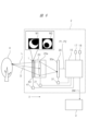
図6は、実施形態2に係る撮像装置の構成例を示す図である。図6に示すように、実施形態2に係る撮像装置2は、光学系部20、撮像素子30、液晶マスク部40と、光学系制御部21、撮像素子制御部31、液晶マスク制御部41、および演算制御部10を有している。なお、図中のz方向は、光学系部20の主軸方向である。
図6は、実施形態2に係る撮像装置の構成例を示す図である。図6に示すように、実施形態2に係る撮像装置2は、光学系部20、撮像素子30、液晶マスク部40と、光学系制御部21、撮像素子制御部31、液晶マスク制御部41、および演算制御部10を有している。なお、図中のz方向は、光学系部20の主軸方向である。
光学系部20は、被写体4からの発光または反射光である光Lを集光し、後述する撮像素子30の受光面30aに結像させる。光学系部20は、レンズ20aを含んでいる。レンズ20aは、例えば、単焦点レンズ、あるいはズームレンズである。レンズ20aは、複数のレンズが組み合わされた複合レンズが一般的であるが、単一のレンズであってもよい。光学系部20は、オートフォーカス方式であってもよいし、固定焦点方式であってもよい。
撮像素子30は、光電変換を行う電子部品である。すなわち、撮像素子30は、レンズ20aから距離D(奥行き)だけ離れた被写体4からの発光または反射光である光Lを、光学系部20を通して撮像素子30の受光面30aに結像させ、その像の光による明暗を電荷の量に光電変換し、それを読み出して電気信号に変換するデバイスである。
撮像素子30は、一般的に2次元アレイ状に列配された複数の光電変換素子を有しており、これら複数の光電変換素子により受光面30aが形成されている。撮像素子30は、被写体4から光学系部20に入射し、光学系部20を通過した光Lが受光面30aで受光されるような位置に、配置される。撮像素子30は、受光面30aで受光した光の強さすなわち明るさを電気信号に変換して画像信号を出力する。撮像素子30は、カラー画像を表すカラー画像信号を出力するものであってもよいし、モノクロ画像を表すモノクロ画像信号を出力するものであってもよい。
撮像素子30は、例えば、CCD(Charge Coupled Devices;電荷結合素子)イメージセンサ、あるいはCOMS(Complementary Metal Oxide Semiconductor;相補性金属酸化膜半導体)イメージセンサなどである。
液晶マスク部40は、光学系部20の被写体4側の前に設けられている。液晶マスク部40は、予め定められた複数のマスクのうち、いずれかを出現させたり、いずれのマスクも出現させなかったりする機能を有する。なお、液晶マスク部40は、光学系部20の内部に設けられてもよい。
本実施形態では、液晶マスク部40は、光学系部20の被写体4側において、上記マスクM1,M2のいずれかが設置された状態にしたり、マスクなしの状態にしたりすることができるように構成されている。液晶マスク部40は、上述の液晶光シャッタ1を有している。
光学系制御部21は、演算制御部10から受信する制御信号に基づいて、光学系部20に含まれる可動部分の位置を調整するものである。光学系制御部21は、例えば駆動モータを有しており、当該駆動モータを動作させることにより、レンズの少なくとも一部を移動させる。
光学系部20が、ズームレンズを含んでいる場合には、光学系制御部21は、ズームレンズを構成するレンズ群の一部を移動させることにより、ズーム倍率を変化させたり、ズームレンズ全体を移動させることにより、フォーカスを調整したりしてもよい。光学系部20が、単焦点レンズを含んでいる場合には、レンズ全体を移動させることにより、フォーカスを調整してもよい。光学系部20が絞り機構を含んでいる場合には、絞り機構を操作することにより、絞りの開口径を調整してもよい。
撮像素子制御部31は、演算制御部10から受信する制御信号に基づいて、撮像素子30から出力される画像信号を読み込むことにより、撮像を実行する。撮像素子制御部31は、読み込んだ画像信号を演算制御部10に送信する。なお、撮像素子30を制御して被写体4を撮像する際のシャッタ方式は、例えば、グローバルシャッタ方式、あるいは、ローリングシャッタ方式であってよい。
液晶マスク制御部41は、演算制御部10から受信する制御信号に基づいて、液晶マスク部40を制御し、液晶マスク部40に意図したマスクMが設置された状態、あるいは、マスクMが設置されていない状態を実現させる。
〈演算制御部の構成例〉
図7は、実施形態2による演算制御部10の構成の例を示す図である。図7に示すように、演算制御部10は、例えば、コンピュータであり、プロセッサ11、メモリ12、およびインタフェース13を有している。
図7は、実施形態2による演算制御部10の構成の例を示す図である。図7に示すように、演算制御部10は、例えば、コンピュータであり、プロセッサ11、メモリ12、およびインタフェース13を有している。
メモリ12は、プロセッサ11が各種の演算処理あるいは画像処理などを実行したり、各種の制御処理を実行したりするのに使用されるプログラムPを格納する。また、メモリ12は、プロセッサ11が処理するデータを一時的または長期的に格納する。
プロセッサ11は、メモリ12に格納されたプログラムPを読み出して実行することにより、演算処理、画像処理、および制御処理を含む各種の処理を実行する。プロセッサ11は、各種の処理を実行する際に、メモリ12内にデータを格納したり、メモリ12内に格納されているデータにアクセスしたりして、処理を実行する。
また、プロセッサ11は、各種処理の一部として、マスクなし撮像処理、代表エッジ方向決定処理、マスク選択処理、第1マスク撮像処理、第2マスク撮像処理、復号化処理、被写体奥行き推定処理、およびデプスマップ生成処理、データ出力処理、および撮像継続判定処理を実行する。これら各種の処理の詳細については後述する。
プロセッサ11は、上記のマスクなし撮像処理、代表エッジ方向決定処理、マスク選択処理、第1マスク撮像処理、第2マスク撮像処理を実行するために、光学系制御部21、撮像素子制御部31、および液晶マスク制御部41に、制御信号を送信する。
インタフェース13は、外部装置3と接続され、演算制御部10内で生成された復号化画像あるいはデプスマップDMを外部装置3に送信する。
なお、上記コンピュータの全部または一部は、DSP(Digital Signal Processor)、ASIC(Application Specific Integrated Circuit)、FPGA(Field Programmable Gate Array)、CPLD(Complex Programmable Logic Device)などの半導体回路により構成されてもよい。
外部装置3は、例えば、画像処理装置、車両運転支援装置などである。画像処理装置は、例えば、撮像画像に対して、光学系からの距離が遠い背景をぼかして注目される被写体を強調するような加工を施す。車両運転支援装置は、例えば、車両周辺の物体の位置あるいは相対的な移動速度などを検出し、危険を回避するために警告を発したり車両を制御したりする。
なお、演算制御部10には、操作部17および表示部18が接続されている。操作部17は、ユーザからの入力操作を受け付けるためのものであり、表示部18は、ユーザに向けた情報を視覚的に出力するためのものである。操作部17は、例えば、キーボード、マウス、ボタン、ダイヤルなどである。表示部18は、例えば、液晶パネル、有機ELパネルなどである。操作部17および表示部18は、一体化されたタッチパネルであってもよい。操作部17および表示部18は、外部装置3側に設けられていてもよい。
〈撮像装置における動作の流れ〉
実施形態2に係る撮像装置における動作の流れについて説明する。
図8は、実施形態2に係る撮像装置2の動作の流れの一例を示すフロー図である。
実施形態2に係る撮像装置における動作の流れについて説明する。
図8は、実施形態2に係る撮像装置2の動作の流れの一例を示すフロー図である。
図8に示すように、ステップS1では、1つ目のマスクM1の形成が行われる。具体的には、演算制御部10が、液晶光シャッタ1にマスクM1が形成されるように、液晶マスク制御部41に制御信号を送信する。液晶マスク制御部41は、受信した制御信号に基づいて、液晶光シャッタ1の各電極に必要な電気信号を印加し、各セグメントの状態を光透過状態または光遮蔽状態に制御することにより、マスクM1が形成された状態を作り出す。
ステップS2では、1つ目のマスクによる被写体の符号化撮像が行われる。具体的には、演算制御部10が、形成されたマスクM1を用いて被写体4が符号化撮像されるように、撮像素子制御部31に、制御信号を送信する。撮像素子制御部31は、受信した制御信号に基づいて、被写体4が撮像されるように、すなわち、撮像素子30の出力信号により表される被写体4の撮像画像P1が演算制御部10に送信されるように、撮像素子30を制御する。
ステップS3では、2つ目のマスクM2の形成が行われる。具体的には、演算制御部10が、液晶光シャッタ1にマスクM2が形成されるように、液晶マスク制御部41に制御信号を送信する。液晶マスク制御部41は、受信した制御信号に基づいて、液晶光シャッタ1の各電極に必要な電気信号を印加し、各セグメントの状態を光透過状態または光遮蔽状態に制御することにより、マスクM2が形成された状態を作り出す。
ステップS4では、2つ目のマスクによる被写体の符号化撮像が行われる。具体的には、演算制御部10が、形成されたマスクM2を用いて被写体4が符号化撮像されるように、撮像素子制御部31に、制御信号を送信する。撮像素子制御部31は、受信した制御信号に基づいて、被写体4が撮像されるように、すなわち、撮像素子30の出力信号により表される被写体4の撮像画像P2が演算制御部10に送信されるように、撮像素子30を制御する。
ステップS5では、撮像画像の復号化が行われる。具体的には、演算制御部10が、得られた撮像画像P1,P2に対して、マスクM1に対応する点拡がり関数およびマスクM2に対応する点拡がり関数に基づく復号化を行う。
ステップS6では、復号化画像および被写体奥行き情報の取得が行われる。具体的には、演算制御部10が、上記復号化によって得られた情報を基に、被写体4の復号化画像と当該復号化画像の各位置に対応する物体の奥行き推定情報とを得る。
ステップS7では、デプスマップの生成が行われる。具体的には、演算制御部10が、得られた復号化画像と奥行き推定情報とに基づいて、被写体4のデプスマップDMを生成する。
ステップS8では、デプスマップの出力が行われる。具体的には、演算制御部10が、生成されたデプスマップDMを、外部装置3に出力する。
このような実施形態2によれば、より実用性の高いDFD技術を提供することができる。より詳しくは、撮像装置2によれば、符号化撮像に用いるマスクの形成を、液晶光シャッタ1により実現している。液晶光シャッタ1は、セグメントの設計次第で、任意のマスクを実現させることができるとともに、マスクの状態の切替えに、ハードウェアを物理的に切り替える必要がない。したがって、マスクの位置を精度良く制御することができ、またマスクを切り替えるための機構も簡単にすることが可能である。
以上、本発明の各種実施形態について説明したが、本発明は上記した実施形態に限定されるものではなく、様々な変形例が含まれる。また、上記した実施形態は本発明を分かりやすく説明するために詳細に説明したものであり、必ずしも説明した全ての構成を備えるものに限定されるものではない。また、ある実施形態の構成の一部を他の実施形態の構成に置き換えることが可能であり、また、ある実施形態の構成に他の実施形態の構成を加えることも可能である。これらは全て本発明の範疇に属するものである。さらに文中や図中に含まれる数値等もあくまで一例であり、異なるものを用いても本発明の効果を損なうものではない。
1…液晶光シャッタ、2…撮像装置、3…外部装置、4…被写体、10…演算制御部、11…プロセッサ、12…メモリ、13…インタフェース、17…操作部、18…表示部、20…光学系部、21…光学系制御部、30…撮像素子、31…撮像素子制御部、40…液晶マスク部、41…液晶マスク制御部、51…第1の偏光板、52…第1のガラス基板、53…光遮蔽層、54…第1の透明電極層、55…第1の配向膜、56…液晶層、57…第2の配向膜、58…第2の透明電極層、59…第2のガラス基板、60…第2の偏光板、61…スペーサ、62…シール層、A2…外側領域、CR1~CR4…セグメント電極、CR5…外周セグメント電極、D…奥行き、K2…開口、L…光、M1,M2,M1a,M2a…マスク、P…プログラム、P1,P2…撮像画像、DM…デプスマップ、R1~R4…セグメント、R5…外周セグメント、RL…光入射領域、T1~T6…状態、V,W…幅、φ1~φ3…直径
Claims (7)
- 符号化撮像に用いられるマスクを形成する液晶光シャッタであって、
第1の透明電極層と、
前記第1の透明電極層に対向して配置され、複数の透明なセグメント電極を有する第2の透明電極層と、
前記第1の透明電極層と前記第2の透明電極層との間に配置される液晶層と、
前記符号化撮像に用いる光学系の光入射領域を含み前記光入射領域よりも広い領域に対応した開口が形成され、前記開口の外側領域において光を遮蔽する光遮蔽層と、を備え、
前記複数のセグメント電極は、前記開口の輪郭が含まれる前記光入射領域の外周領域に対応した外周セグメント電極を含み、
前記第1の透明電極層と前記複数のセグメント電極の各々とに印加される電気信号が制御されることにより前記マスクが形成される、
液晶光シャッタ。 - 請求項1に記載の液晶光シャッタにおいて、
前記光入射領域は、円領域であり、
前記外周セグメント電極は、環形状を有する、
液晶光シャッタ。 - 請求項1に記載の液晶光シャッタにおいて、
前記第1の透明電極層と前記複数のセグメント電極の各々とに印加される電気信号が制御されることにより、互いに異なる複数の前記マスクが形成される、
液晶光シャッタ。 - 請求項1に記載の液晶光シャッタにおいて、
前記外周セグメント電極に対応するセグメントは、前記マスクが形成される場合に、光遮蔽状態となる、
液晶光シャッタ。 - 請求項2に記載の液晶光シャッタにおいて、
前記外周セグメント電極の幅は、10μm以上、30μm以下である、
液晶光シャッタ。 - 請求項3に記載の液晶光シャッタにおいて、
前記複数のセグメント電極のうち、複数の前記マスクを形成する場合に共通して光遮蔽状態となるセグメントに対応する2以上のセグメント電極は、前記外周セグメント電極を含み、互いに接続される、
液晶光シャッタ。 - 請求項1から請求項6のいずれか一項に記載の液晶光シャッタを備える撮像装置。
Priority Applications (2)
| Application Number | Priority Date | Filing Date | Title |
|---|---|---|---|
| JP2024551261A JPWO2024079997A1 (ja) | 2022-10-12 | 2023-08-23 | |
| US19/097,072 US20250231446A1 (en) | 2022-10-12 | 2025-04-01 | Liquid crystal optical shutter and imaging device |
Applications Claiming Priority (2)
| Application Number | Priority Date | Filing Date | Title |
|---|---|---|---|
| JP2022-164120 | 2022-10-12 | ||
| JP2022164120 | 2022-10-12 |
Related Child Applications (1)
| Application Number | Title | Priority Date | Filing Date |
|---|---|---|---|
| US19/097,072 Continuation US20250231446A1 (en) | 2022-10-12 | 2025-04-01 | Liquid crystal optical shutter and imaging device |
Publications (1)
| Publication Number | Publication Date |
|---|---|
| WO2024079997A1 true WO2024079997A1 (ja) | 2024-04-18 |
Family
ID=90669374
Family Applications (1)
| Application Number | Title | Priority Date | Filing Date |
|---|---|---|---|
| PCT/JP2023/030332 Ceased WO2024079997A1 (ja) | 2022-10-12 | 2023-08-23 | 液晶光シャッタおよび撮像装置 |
Country Status (3)
| Country | Link |
|---|---|
| US (1) | US20250231446A1 (ja) |
| JP (1) | JPWO2024079997A1 (ja) |
| WO (1) | WO2024079997A1 (ja) |
Citations (3)
| Publication number | Priority date | Publication date | Assignee | Title |
|---|---|---|---|---|
| WO2011129055A1 (ja) * | 2010-04-13 | 2011-10-20 | パナソニック株式会社 | ブラー補正装置およびブラー補正方法 |
| WO2012008337A1 (ja) * | 2010-07-16 | 2012-01-19 | オリンパス株式会社 | 撮像装置 |
| WO2022059279A1 (ja) * | 2020-09-18 | 2022-03-24 | 株式会社ジャパンディスプレイ | カメラモジュール |
-
2023
- 2023-08-23 JP JP2024551261A patent/JPWO2024079997A1/ja active Pending
- 2023-08-23 WO PCT/JP2023/030332 patent/WO2024079997A1/ja not_active Ceased
-
2025
- 2025-04-01 US US19/097,072 patent/US20250231446A1/en active Pending
Patent Citations (3)
| Publication number | Priority date | Publication date | Assignee | Title |
|---|---|---|---|---|
| WO2011129055A1 (ja) * | 2010-04-13 | 2011-10-20 | パナソニック株式会社 | ブラー補正装置およびブラー補正方法 |
| WO2012008337A1 (ja) * | 2010-07-16 | 2012-01-19 | オリンパス株式会社 | 撮像装置 |
| WO2022059279A1 (ja) * | 2020-09-18 | 2022-03-24 | 株式会社ジャパンディスプレイ | カメラモジュール |
Also Published As
| Publication number | Publication date |
|---|---|
| JPWO2024079997A1 (ja) | 2024-04-18 |
| US20250231446A1 (en) | 2025-07-17 |
Similar Documents
| Publication | Publication Date | Title |
|---|---|---|
| CN101371568B (zh) | 复眼方式的照相机模块及其制造方法 | |
| US20120019736A1 (en) | Imaging device | |
| US10110811B2 (en) | Imaging module and imaging device | |
| JP2008216626A (ja) | 可変焦点レンズ | |
| CN103348668B (zh) | 光场摄像装置以及摄像元件 | |
| CN105472357A (zh) | 成像方法、成像装置和拍摄系统 | |
| US7768711B2 (en) | Manufacturing method of light-collecting device, light-collecting device and phase shift mask | |
| CN111201481B (zh) | 相位调制装置 | |
| JPWO2006046396A1 (ja) | カメラモジュール | |
| WO2024079997A1 (ja) | 液晶光シャッタおよび撮像装置 | |
| CN102971666B (zh) | 减光装置以及摄像装置 | |
| JP6123250B2 (ja) | 液晶装置、液晶装置の製造方法、及び電子機器 | |
| US20250124585A1 (en) | Imaging apparatus, subject depth estimation method, and program | |
| JP6442065B2 (ja) | フォーカス装置,撮像システムおよびフォーカス駆動信号出力方法 | |
| JP2014085517A (ja) | 液晶装置、及び電子機器 | |
| CN109313379A (zh) | 图像摄像装置及滤光片 | |
| US8848276B2 (en) | Optical-path conversion device and imaging apparatus | |
| JPH10229181A (ja) | 固体撮像装置とその製造方法 | |
| US20250238943A1 (en) | Imaging device, method of estimating subject depth, and program | |
| JPH06148593A (ja) | 光量調整装置を有した光学系 | |
| JPWO2022137807A5 (ja) | ||
| US20210105412A1 (en) | Image sensor with pixelated cutoff filter for phase detection autofocus | |
| JP2011082795A (ja) | 撮像装置及びデジタルカメラ | |
| CN116300272A (zh) | 投影设备、投影设备调整方法、系统、介质及产品 | |
| WO2020261852A1 (ja) | 投影装置 |
Legal Events
| Date | Code | Title | Description |
|---|---|---|---|
| 121 | Ep: the epo has been informed by wipo that ep was designated in this application |
Ref document number: 23877005 Country of ref document: EP Kind code of ref document: A1 |
|
| WWE | Wipo information: entry into national phase |
Ref document number: 2024551261 Country of ref document: JP |
|
| NENP | Non-entry into the national phase |
Ref country code: DE |
|
| 122 | Ep: pct application non-entry in european phase |
Ref document number: 23877005 Country of ref document: EP Kind code of ref document: A1 |