WO2024079989A1 - 検出機能付き表示装置 - Google Patents
検出機能付き表示装置 Download PDFInfo
- Publication number
- WO2024079989A1 WO2024079989A1 PCT/JP2023/029854 JP2023029854W WO2024079989A1 WO 2024079989 A1 WO2024079989 A1 WO 2024079989A1 JP 2023029854 W JP2023029854 W JP 2023029854W WO 2024079989 A1 WO2024079989 A1 WO 2024079989A1
- Authority
- WO
- WIPO (PCT)
- Prior art keywords
- light
- unit
- display device
- detection function
- function according
- Prior art date
- Legal status (The legal status is an assumption and is not a legal conclusion. Google has not performed a legal analysis and makes no representation as to the accuracy of the status listed.)
- Ceased
Links
Images


Classifications
-
- G—PHYSICS
- G01—MEASURING; TESTING
- G01S—RADIO DIRECTION-FINDING; RADIO NAVIGATION; DETERMINING DISTANCE OR VELOCITY BY USE OF RADIO WAVES; LOCATING OR PRESENCE-DETECTING BY USE OF THE REFLECTION OR RERADIATION OF RADIO WAVES; ANALOGOUS ARRANGEMENTS USING OTHER WAVES
- G01S7/00—Details of systems according to groups G01S13/00, G01S15/00, G01S17/00
- G01S7/48—Details of systems according to groups G01S13/00, G01S15/00, G01S17/00 of systems according to group G01S17/00
- G01S7/481—Constructional features, e.g. arrangements of optical elements
-
- G—PHYSICS
- G06—COMPUTING OR CALCULATING; COUNTING
- G06F—ELECTRIC DIGITAL DATA PROCESSING
- G06F3/00—Input arrangements for transferring data to be processed into a form capable of being handled by the computer; Output arrangements for transferring data from processing unit to output unit, e.g. interface arrangements
- G06F3/01—Input arrangements or combined input and output arrangements for interaction between user and computer
- G06F3/03—Arrangements for converting the position or the displacement of a member into a coded form
- G06F3/041—Digitisers, e.g. for touch screens or touch pads, characterised by the transducing means
- G06F3/042—Digitisers, e.g. for touch screens or touch pads, characterised by the transducing means by opto-electronic means
Definitions
- This disclosure relates to a display device with a detection function.
- a first display device with detection function has a display unit with a light-transmitting region, and a light-emitting unit and a light-receiving unit arranged on the back side of the display unit, and is equipped with a sensor unit that measures the distance to an object within a specific distance range by measuring the flight time of light emitted from the light-emitting unit, which passes through the transmittance region and is reflected by an object within a specific distance range from the display unit, passes through the transmittance region and is received by the light-receiving unit.
- a second display device with detection function has a display unit having a light-transmitting region, and a light-emitting unit and a light-receiving unit arranged on the back side of the display unit, and is equipped with a sensor unit that measures the distance to an object within a specific distance range by measuring the flight time of light emitted from the light-emitting unit, which passes through the transmittance region and is reflected by an object within a specific distance range from the display unit, passes through the transmittance region and is received by the light-receiving unit, and the light-receiving unit has a light-receiving element and a switching element that activates the light-receiving element at the timing of receiving reflected light from an object within the specific distance range based on a timing signal indicating the effective period of distance measurement.
- a sensor unit having a light-emitting unit and a light-receiving unit arranged on the back side of the display unit measures the distance to an object within a specific distance range by measuring the flight time until light emitted from the light-emitting unit is reflected by the object within a specific distance range and received by the light-receiving unit.
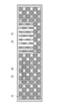
- FIG. 1 is a cross-sectional view that illustrates a schematic configuration example of a display device with a detection function according to an embodiment of the present disclosure.
- FIG. 2 is a plan view illustrating an example of a pixel structure of the display device with a detection function according to the embodiment.
- FIG. 3 is a cross-sectional view that illustrates a schematic modification of the pixel structure according to the embodiment.
- FIG. 4 is a plan view that illustrates a modification of the pixel structure of the display device with a detection function according to the embodiment.
- FIG. 5 is a cross-sectional view that illustrates a schematic modification of the display device with a detection function according to the embodiment.
- FIG. 1 is a cross-sectional view that illustrates a schematic configuration example of a display device with a detection function according to an embodiment of the present disclosure.
- FIG. 2 is a plan view illustrating an example of a pixel structure of the display device with a detection function according to the embodiment.
- FIG. 3 is a cross
- FIG. 6 is a cross-sectional view illustrating a schematic modification of the light receiving portion of the display device with a detection function according to one embodiment.
- FIG. 7 is a plan view illustrating an example of a module structure of a display device with a detection function according to an embodiment.
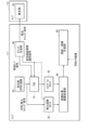
- FIG. 8 is a block diagram illustrating a first example of a circuit configuration of a display device with a detection function according to one embodiment.
- FIG. 9 is a timing chart showing an example of a detection process performed by the display device with a detection function according to one embodiment.
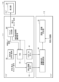
- FIG. 10 is a block diagram illustrating a second example of the circuit configuration of the display device with a detection function according to one embodiment.
- FIG. 11 is a circuit diagram illustrating an example of the configuration per pixel of the light receiving section in the second example of the configuration shown in FIG.
- FIG. 12 is a circuit diagram illustrating an example of the operation of the pixels of the light receiving section in the second configuration example shown in FIG.
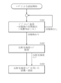
- FIG. 13 is a flowchart illustrating a first example of the recognition and authentication process performed by the display device with a detection function according to an embodiment.
- FIG. 14 is a flowchart illustrating a second example of the recognition and authentication process performed by the display device with a detection function according to an embodiment.
- FIG. 15 is a flowchart illustrating a third example of the recognition and authentication process performed by the display device with a detection function according to an embodiment.
- FIG. 16 is a flowchart illustrating a fourth example of the recognition and authentication process performed by the display device with a detection function according to an embodiment.
- FIG. 17 is a block diagram illustrating a first example of a chip configuration of a display device with a detection function according to one embodiment.
- FIG. 18 is a block diagram illustrating a second example of a chip configuration of a display device with a detection function according to one embodiment.
- FIG. 19 is a block diagram illustrating a third example of a chip configuration of a display device with a detection function according to an embodiment.
- FIG. 20 is a block diagram illustrating a fourth example of a chip configuration of a display device with a detection function according to an embodiment.
- FIG. 21 is a block diagram illustrating a fifth example of a chip configuration of a display device with a detection function according to one embodiment.
- Fig. 1 is a schematic diagram showing a configuration example of a display device with a detection function according to an embodiment of the present disclosure
- Fig. 2 is a schematic diagram showing an example of a pixel structure of the display device with a detection function according to the embodiment.
- the display device with detection function includes a display unit 1 and a sensor unit 2 having a light-emitting unit 20 and a light-receiving unit 30 arranged on the rear side of the display unit 1.
- the display unit 1 has a pixel unit 10.
- a protective glass 11 is disposed on the surface of the pixel unit 10.
- a protective film 12 may be disposed on the surface of the protective glass 11.
- the pixel section 10 includes an image display array in which a plurality of display pixels are arranged in a two-dimensional array.
- the plurality of display pixels may be light emitters that emit light in visible wavelengths, such as OLEDs (Organic Electro Luminescence Diodes).
- the plurality of display pixels include, for example, R (red) pixels 10R, G (green) pixels 10G, and B (blue) pixels 10B.
- the display unit 1 has a light-transmitting region that transmits light between the front and back surfaces.
- the display unit 1 includes, as its transmissive regions, a first transmissive region 70 provided in the optical path through which the emitted light L1 from the light-emitting unit 20 passes, and a second transmissive region 80 provided in the optical path through which the reflected light L2 from the object 200 within a specific distance range Da passes before being received by the light-receiving unit 30.
- the surface density of the multiple display pixels may be uniform over the entire surface. When the surface density is uniform over the entire surface, no special structure is required, and the display unit 1 can be realized at low cost.
- the surface density of the multiple display pixels in at least one of the first transmissive region 70 and the second transmissive region 80 may be lower than the surface density of the multiple display pixels in regions other than the transmissive regions.
- the surface density of the multiple display pixels in at least the second transmissive region 80 is lower than the surface density of the multiple display pixels in regions other than the second transmissive region 80.
- FIG. 1 and 2 show an example configuration in which the surface density of the display pixels in the first transmissive region 70 in the display unit 1 is lower than the surface density of the display pixels in regions other than the first transmissive region 70.
- the transmittance of the emitted light L1 from the light-emitting unit 20 in the display unit 1 can be increased, and the emitted light L1 can be efficiently irradiated onto the object 200, improving distance measurement and recognition accuracy.
- FIGS. 3 and 4 show schematic diagrams of modified pixel structures of a display device with detection function according to one embodiment.
- An example configuration is shown in which the surface density of the plurality of display pixels in the second transmissive region 80 is lower than the surface density of the plurality of display pixels in regions other than the second transmissive region 80.
- the transmittance of the reflected light L2 to the light receiving unit 30 in the display unit 1 can be increased, and the amount of light received by the light receiving unit 30 can be improved, improving distance measurement and recognition accuracy.
- the light-emitting unit 20 and the light-receiving unit 30 are disposed within the housing 3.
- a condensing lens 40 is provided between the light-emitting unit 20 and the display unit 1.
- an optical filter 50 and a condensing lens 60 are provided between the light-receiving unit 30 and the display unit 1.
- the structure of the focusing lens 40 and the focusing lens 60 is not particularly limited, but the use of a Fresnel lens or a metasurface is expected to have the effect of making the housing 3 thinner.
- the optical filter 50 selectively passes light that includes the wavelength band of the emitted light L1 from the light emitting unit 20.
- the sensor unit 2 can measure the distance to the object 200, for example, by the dToF (direct time of flight) method.
- the dToF method is a method for measuring the distance to the object 200 by irradiating the object 200 with light, receiving the reflected light L2 from the object 200, and measuring the flight time of the light.
- a TDC (Time to Digital Converter) 91 (see FIG. 8, etc.), which will be described later, can be used to measure the flight time.
- the TDC 91 converts the elapsed time into a digital signal.
- the TDC 91 sequentially generates a time series of time codes from the start of irradiation of the object 200 with light, and captures the time code generated when the reflected light L2 is received.
- the flight time of the light can be detected by outputting a digital signal of the elapsed time corresponding to the captured time code.
- the sensor unit 2 measures the distance to the object 200 within the specific distance range Da by measuring the flight time of the light emitted from the light-emitting unit 20, passing through the first transparent region 70, being reflected by the object 200 within the specific distance range Da from the display unit 1, passing through the second transparent region 80, and being received by the light-receiving unit 30.
- the sensor unit 2 excludes reflected light L2 from positions outside the specific distance range Da from the distance measurement target based on a timing signal (valid distance measurement period identification signal) ( Figure 9 ( Figure A)) indicating the valid period of distance measurement described later.
- the display device with detection function may generate at least one of a reflected light intensity map (reflected light intensity image) and a depth map (depth image) based on the distance measurement results by the sensor unit 2. Then, at least one of a recognition process and an authentication process may be performed on the target object 200 based on at least one of the reflected light intensity map and the depth map.
- the light-emitting unit 20 has at least one light source 21 that emits light at a wavelength outside the visible wavelength range.
- the light source 21 may be a laser diode that emits, for example, pulsed near-infrared light as the emitted light L1.
- the structure of the light source 21 and the control of the driver that drives the light source 21 are simplified, and it can be realized at low cost. Furthermore, compared to when there are multiple light sources 21, there is no effect of variations in the emission intensity between the multiple light sources 21, so a uniform amount of light suitable for authentication can be obtained.
- FIG. 5 shows a schematic diagram of a modified example of the light-emitting unit 20.
- the light-emitting unit 20 may have a configuration having multiple light-emitting sources 21.
- the multiple light-emitting sources 21 may be arranged in a two-dimensional array.
- an ROI Region of Interest
- ROI Region of Interest
- the light receiving unit 30 has a plurality of light receiving pixels.
- the plurality of light receiving pixels may be light receiving elements 31 consisting of, for example, single photon avalanche diodes (SPADs).
- a SPAD is an avalanche photodiode (APD) that improves the charge multiplication effect by applying a reverse bias voltage exceeding the breakdown voltage.
- a SPAD the charge generated by photoelectric conversion increases rapidly due to the high multiplication effect. This increased charge causes a current with a steep rise to flow through the SPAD. By detecting this current and generating a pulse signal, the incidence of a single photon can be detected. This operating mode is called the Geiger mode.
- the multiple light receiving pixels may be SPAD pixels arranged in a two-dimensional array.
- the multiple light receiving elements 31 are arranged in a two-dimensional array structure, for example, after identifying the position and size of the object 200, power can be reduced by activating only the light receiving pixels in the area corresponding to the object 200. It is also possible to reduce unnecessary light L3 from sources other than the object 200.
- the multiple light receiving elements 31 and a circuit including a TDC 91 may be formed on the same substrate. In this case, it is possible to reduce the thickness of the sensor section 2, improving the design freedom of the product.
- FIG. 6 shows a schematic diagram of a modified example of the light receiving unit 30.
- a circuit including a TDC 91 (FIG. 8, etc.) described later may be formed on a substrate 32 different from the substrate 32 on which the plurality of light receiving elements 31 are formed.
- a substrate on which a plurality of light receiving elements 31 are formed may be stacked on a substrate 32 on which a circuit including a TDC 91 is formed, and the plurality of light receiving elements 31 and the TDC 91 may be electrically connected to form a stacked sensor structure. This allows the pixel pitch of the plurality of light receiving pixels to be narrowed. The spatial resolution required for authentication can be achieved with a small chip, making it possible to reduce costs.
- the area of the second transmissive region 80 can be reduced, so that deterioration of the image quality of the display unit 1 (image quality difference between the second transmissive region 80 and the region other than the second transmissive region 80) can be reduced.
- FIG. 7 shows a schematic diagram of an example of a module structure of a display device with detection function according to one embodiment.
- an RGB sensor 4 for acquiring an RGB image may be installed as another sensor.
- a reflected light intensity image or a depth image acquired based on the detection result of the sensor unit 2 may be combined with an RGB image acquired by the RGB sensor 4 to perform at least one of a recognition process and an authentication process.
- the RGB sensor 4 and the sensor unit 2 are arranged in a close position. The shorter the distance (baseline length) between the two sensors, the RGB sensor 4 and the sensor unit 2, the smaller the correction calculation cost. In addition, the shorter the distance between the sensors, the higher the spatial resolution. Note that the structure of the RGB sensor 4 is not limited to being solved.
- the RGB sensor 4 may be arranged on the back side of the display unit 1, similar to the sensor unit 2.
- Fig. 8 shows a first example of the circuit configuration of a display device with a detection function according to one embodiment.
- Fig. 8 shows the circuit configuration of a portion related to distance measurement, recognition processing, and authentication processing in the display device with a detection function.
- Fig. 9 shows a timing chart showing an example of detection processing by the display device with a detection function according to one embodiment.
- Fig. 9 shows a timing chart of a light emission timing signal (Fig. 9(A)), a time code signal (Fig. 9(B)), a valid distance measurement period identification signal (Fig. 9(C)), a SPAD firing timing signal (Fig. 9(D)), and an output of a TDC 91 (Fig. 9(E)).
- the display device with detection function has a light emitting unit 20, a light receiving unit 30, a timing generating unit 90, a TDC 91, a histogram counter 92, a firing count counter 93, a distance calculation/image processing unit 94, and an authentication/recognition calculation unit 95.
- the timing generation unit 90 generates an emission timing signal ((A) in FIG. 9) for the light source 21 in the light emission unit 20 and outputs it to the light emission unit 20.
- the timing generation unit 90 also generates a time code signal ((B) in FIG. 9) that indicates the elapsed time from the emission of the emitted light L1 in the light emission unit 20 and outputs it to the TDC 91.
- the timing generation unit 90 also generates an effective ranging period identification signal ((C) in FIG. 9) and outputs it to the TDC 91.
- the timing generation unit 90 may also output the effective ranging period identification signal to the firing count counter 93.
- the TDC 91 generates a digital signal (Figure 9 (E)) corresponding to the flight time of the light emitted from the light emitting unit 20, reflected by the target object 200, and received by the light receiving unit 30, based on the SPAD firing timing signal ( Figure 9 (D)) from the light receiving unit 30 and the time code signal and valid ranging period identification signal from the timing generating unit 90.
- the valid distance measurement period identification signal is a timing signal that indicates a valid period of distance measurement and an invalid period of distance measurement.
- the valid period of distance measurement is a period that corresponds to the valid distance range of distance measurement, and is a period that includes the timing when the light emitted from the light emitting unit 20 (emitted light L1) is reflected by the object 200 within a specific distance range Da and is received by the light receiving unit 30 as reflected light L2.
- the valid period of distance measurement is set so as not to include the timing when the unnecessary light L3 is received by the light receiving unit 30.
- the invalid period of distance measurement is a period that includes the timing when the unnecessary light L3 is received by the light receiving unit 30. Therefore, the valid distance measurement period identification signal can control the valid distance range of distance measurement.
- the unnecessary light L3 is, for example, light generated by the emitted light from the light emitting unit 20 being reflected by the protective glass 11, the protective film 12, etc. This allows the SPAD firing timing signal based on reflected light (unwanted light L3) from a position outside the specific distance range Da to be excluded from the distance measurement, and the SPAD firing timing signal based only on reflected light L2 from the specific distance range Da to be the target of distance measurement.
- the histogram counter 92 generates a histogram of flight times based on the digital signal indicating the flight times output from the TDC 91.
- the generated histogram of flight times is output to the distance calculation/image processing unit 94.
- the firing count counter 93 counts the number of firings of the SPAD pixel based on the valid ranging period identification signal and the SPAD firing timing signal ((D) in FIG. 9) from the light receiving unit 30.
- the firing count counter 93 counts the number of firings only during the valid ranging period based on the valid ranging period identification signal, and is therefore able to count the number of firings based only on the reflected light L2 from a specific distance range Da.
- the distance calculation/image processing unit 94 calculates the distance to the object 200 based on the counter value from the firing count counter 93 and the histogram from the histogram counter 92, and generates at least one of a reflected light intensity map and a depth map based on the distance calculation result.
- the authentication/recognition calculation unit 95 is a calculation unit that performs at least one of a recognition process and an authentication process on the target object 200 based on at least one of a reflected light intensity map and a depth map.
- An RGB image acquired by the RGB sensor 4 (FIG. 7) may be input to the authentication/recognition calculation unit 95.
- the authentication/recognition calculation unit 95 may combine at least one of a reflected light intensity map and a depth map with the RGB image acquired by the RGB sensor 4 to perform at least one of a recognition process and an authentication process.
- ranging control can be achieved with a pure logic circuit.
- FIG. 10 shows a second example of the circuit configuration of a display device with a detection function according to one embodiment.
- an effective distance measurement period identification signal is supplied to the light receiving unit 30.
- the SPAD pixel by deactivating the SPAD pixel during the non-effective distance measurement period, the SPAD firing timing signal based on reflected light (unwanted light L3) from a position outside the specific distance range Da can be excluded from the distance measurement target, and the SPAD firing timing signal based only on reflected light L2 from the specific distance range Da can be included in the distance measurement target.
- the SPAD pixel can be deactivated by not applying a reverse bias voltage (breakdown voltage) that would cause the light receiving element 31 to enter Geiger mode.
- FIG. 11 shows a schematic diagram of a configuration example of one SPAD pixel of the light receiving section 30 in the second configuration example shown in FIG. 10. Note that FIG. 11 shows a configuration example in which the light receiving element 31 is cathode readout.
- FIG. 12 shows a schematic diagram of an operation example of the SPAD pixel of the light receiving section 30 in the second configuration example shown in FIG. 10.
- the light receiving unit 30 has, for each SPAD pixel, a light receiving element 31, a constant current source 102, a buffer amplifier 103, an NMOS (Metal Oxide Semiconductor) transistor 104, and an inverter 105.
- a constant current source 102 for each SPAD pixel, a light receiving element 31, a constant current source 102, a buffer amplifier 103, an NMOS (Metal Oxide Semiconductor) transistor 104, and an inverter 105.
- NMOS Metal Oxide Semiconductor
- the light receiving element 31 is activated by applying a reverse bias voltage exceeding the breakdown voltage as shown in FIG. 12, and enters the Geiger mode in which it can detect the incidence of photons.
- a negative anode voltage is applied to the anode of the light receiving element 31.
- the cathode of the light receiving element 31 is connected to a constant current source 102 that supplies the power supply voltage VDD, a buffer amplifier 103, and an NMOS transistor 104.
- the buffer amplifier 103 amplifies the signal generated by the light receiving element 31 and outputs it to the TDC 91 as a light receiving signal.
- the inverter 105 receives an effective distance measurement period identification signal.
- the NMOS transistor 104 is a switching element that activates the light receiving element 31 at the timing of receiving reflected light L2 from an object 200 within a specific distance range Da, based on the effective distance measurement period identification signal input via the inverter 105.
- the NMOS transistor 104 is connected to the cathode of the light receiving element 31, the constant current source 102 (a specified voltage line), and the buffer amplifier 103.
- the NMOS transistor 104 controls the applied voltage so that the cathode-anode voltage is below the breakdown voltage during the non-effective period of distance measurement based on the effective distance measurement period identification signal.
- the applied voltage is controlled by connecting a PMOS transistor as a switching element to the anode of the light receiving element 31. This makes it possible to control the effective distance range for distance measurement by the switching operation of the NMOS transistor 104 or PMOS transistor as a switching element.
- the SPAD pixel is inactive during the ineffective period of distance measurement, so power consumption can be reduced. Furthermore, the detection accuracy of the reflected light L2 from the object 200 at close range can be improved.
- FIG. 13 shows a flowchart illustrating a first example of the recognition and authentication process performed by the display device with a detection function according to one embodiment.
- the distance calculation/image processing unit 94 When authentication by a user is started, for example, by starting an authentication application, the distance calculation/image processing unit 94 first acquires a depth map (step S101). The distance calculation/image processing unit 94 also detects the presence or absence of the object 200. The distance calculation/image processing unit 94 may also determine the authenticity of the object 200. If the object 200 is not detected, the distance calculation/image processing unit 94 repeats the process of step S101. On the other hand, if it is determined that the object 200 has been detected, the distance calculation/image processing unit 94 then acquires a reflected light intensity map (step S102).
- the sensor unit 2 may limit the target region (ROI) of distance measurement when performing the next (at least one) recognition/authentication process based on at least one of the reflected light intensity map and the depth map. For example, when performing recognition and authentication processing again for the same object 200, the distance calculation and image processing unit 94 may generate a reflected light intensity map and a depth map based on the distance measurement results with the target area limited.
- the sensor unit 2 may set an ROI in the light receiving unit 30 according to the position and size of the object 200 determined based on at least one of the reflected light intensity map and the depth map. This may activate only the light receiving pixels in the area corresponding to the object 200. The same applies to the second to fourth examples shown in Figures 14 to 16 described later.
- the authentication/recognition calculation unit 95 uses the reflected light intensity map to perform at least one of the recognition process and the authentication process (step S103). Note that the authentication/recognition calculation unit 95 can also perform at least one of the recognition process and the authentication process by adding an image acquired by another sensor such as the RGB sensor 4 ( Figure 7).
- the reflected light intensity map and the depth map are acquired at different times. Furthermore, only the reflected light intensity map is used for the recognition process or authentication process.
- FIG. 14 shows a flowchart illustrating a second example of the recognition and authentication process performed by a display device with a detection function according to one embodiment.
- the processes in steps S101 and S102 are the same as those in the first example (FIG. 13).
- the authentication/recognition calculation unit 95 performs at least one of the recognition process and the authentication process using the reflected light intensity map and the depth map (step S203). Note that the authentication/recognition calculation unit 95 can also perform at least one of the recognition process and the authentication process by adding an image acquired by another sensor such as the RGB sensor 4 (FIG. 7).
- the reflected light intensity map and the depth map are acquired at different times.
- the reflected light intensity map and the depth map are used for the recognition process or authentication process.
- FIG. 15 shows a flowchart illustrating a third example of the recognition and authentication process performed by a display device with a detection function according to one embodiment.
- the distance calculation/image processing unit 94 When the user starts authentication, for example, by starting an authentication application, the distance calculation/image processing unit 94 first acquires a reflected light intensity map and a depth map (step S301). The distance calculation/image processing unit 94 also detects the presence or absence of the object 200. The distance calculation/image processing unit 94 may also determine the authenticity of the object 200. If the object 200 is not detected, the distance calculation/image processing unit 94 repeats the process of step S301. On the other hand, if it is determined that the object 200 has been detected, the authentication/recognition calculation unit 95 then uses the reflected light intensity map to perform at least one of the recognition process and the authentication process (step S302). The authentication/recognition calculation unit 95 can also perform at least one of the recognition process and the authentication process by adding an image acquired by another sensor such as the RGB sensor 4 (FIG. 7).
- the reflected light intensity map and the depth map are acquired at the same time. Furthermore, only the reflected light intensity map is used for the recognition process or authentication process.
- FIG. 16 shows a flowchart illustrating a fourth example of the recognition and authentication process performed by a display device with a detection function according to one embodiment.
- step S301 the process of step S301 is the same as that of the third example (FIG. 15).
- the authentication/recognition calculation unit 95 performs at least one of the recognition process and the authentication process using the reflected light intensity map and the depth map (step S402). Note that the authentication/recognition calculation unit 95 can also perform at least one of the recognition process and the authentication process by adding an image acquired by another sensor such as the RGB sensor 4 (FIG. 7).
- the reflected light intensity map and the depth map are acquired at the same time.
- the reflected light intensity map and the depth map are used for the recognition process or authentication process.
- FIG. 17 shows a schematic diagram of a first example of a chip configuration for a display device with detection function according to one embodiment.
- the circuits involved in distance measurement, recognition processing, and authentication processing in the display device with detection function may be configured as a single chip 111 as a whole.
- distance measurement to recognition processing or authentication processing can be achieved with a single sensor chip, so that in a product (e.g., a smartphone) in which a display device with detection function is mounted, the recognition processing or authentication processing can be performed while the computational resources are used for other purposes.
- the recognition processing or authentication processing can be performed autonomously with a single sensor chip, if the recognition processing or authentication processing fails, the recognition processing or authentication processing can be performed again immediately.
- FIG. 18 shows a schematic diagram of a second example of a chip configuration for a display device with detection function according to one embodiment.
- the circuit portion excluding the light emitting unit 20 may be configured in one chip 111, and the light emitting unit 20 may be configured in another chip 112.
- the computational resources can be used for other purposes while performing the recognition processing or authentication processing.
- the recognition processing or authentication processing can be performed autonomously with one sensor chip, the recognition processing or authentication processing can be performed again immediately when the recognition processing or authentication processing fails.
- the light emitting unit 20 is configured with a separate chip 112, the freedom of selection of the light emitting source 21 increases.
- this configuration is effective when the light emitting source 21 requires a high voltage that cannot be handled by the manufacturing process of the chip 111.
- FIG. 19 shows a schematic diagram of a third example of a chip configuration for a display device with detection function according to one embodiment.
- the circuit portion excluding the light emitting unit 20, the distance calculation/image processing unit 94, and the authentication/recognition calculation unit 95 may be configured on one chip 111, the light emitting unit 20 may be configured on another chip 112, and the distance calculation/image processing unit 94 and the authentication/recognition calculation unit 95 may be configured on yet another chip 113.
- the light emitting unit 20 is configured on a separate chip 112, the freedom of selection of the light source 21 increases. For example, this configuration is effective when the light emitting source 21 requires a high voltage that cannot be handled by the manufacturing process of the chip 111.
- the sensor chips (chips 111, 112) are placed on the back surface of the display unit 1, there may be restrictions on the mounting position and area.
- the distance calculation/image processing unit 94 and the authentication/recognition calculation unit 95 which are the calculation units, on a chip 113 separate from the sensor chip, for example an application processor, the amount of memory available to the calculation unit can be increased, enabling highly accurate recognition processing and authentication processing.
- FIG. 20 shows a schematic diagram of a fourth example of a chip configuration of a display device with a detection function according to one embodiment.
- FIG. 21 shows a schematic diagram of a fifth example of a chip configuration of a display device with a detection function according to one embodiment.
- the circuitry of the parts involved in distance measurement, recognition processing, and authentication processing in the display device with detection function, except for the authentication/recognition calculation unit 95 may be configured on one chip 111, and the authentication/recognition calculation unit 95 may be configured on another chip 114.
- the circuitry of the parts involved in distance measurement, recognition processing, and authentication processing in the display device with detection function, except for the light-emitting unit 20 and the authentication/recognition calculation unit 95 may be configured on one chip 111, the light-emitting unit 20 may be configured on another chip 112, and the authentication/recognition calculation unit 95 may be configured on yet another chip 114.
- the authentication/recognition calculation unit 95 which is a calculation unit, on a chip 114 other than the sensor chip, such as an application processor, the amount of memory available to the calculation unit can be increased, enabling highly accurate recognition processing and authentication processing.
- the distance to the object 200 within the specific distance range Da is measured by measuring the flight time until the light emitted from the light-emitting unit 20 is reflected by the object 200 within the specific distance range Da and is received by the light-receiving unit 30. This makes it possible to improve the detection accuracy of the object 200 within the specific distance range Da.
- the display device with detection function of one embodiment by using a technology capable of detecting only a specific distance, which is a feature of dToF, it is possible to obtain a reflected light image and a depth image from which the effects of interference light (unwanted light L3) caused by the protective glass 11 or protective film 12 of the display unit 1 have been removed, without using image processing.
- This makes it possible to significantly reduce the image processing required for authenticity determination, recognition processing, and authentication processing of the object 200.
- This makes it possible to reduce the power required for image processing and avoid occupancy of computational resources.
- the stereo method, iToF (Indirect ToF), and Structured Light method do not allow selective exposure according to distance, making it difficult to avoid interference light when measuring distance.
- a display device with a detection function according to an embodiment can be applied to recognition or authentication processes in the following products, for example.
- Authentication processing on smartwatches for example, displaying personal information (emails and schedules) only when a specific user has been authenticated.
- the present technology can be configured as follows.
- the present technology having the following configuration, in a sensor unit having a light emitting unit and a light receiving unit arranged on the back side of a display unit, the light emitted from the light emitting unit is reflected by an object within a specific distance range, and the flight time until the light is received by the light receiving unit is measured, thereby measuring the distance to the object within the specific distance range. This makes it possible to improve the detection accuracy of the object within the specific distance range.
- a display unit having a light transmitting area; a sensor unit having a light-emitting unit and a light-receiving unit arranged on the back side of the display unit, the sensor unit measuring a flight time of light emitted from the light-emitting unit, which passes through the transparent area, is reflected by an object within a specific distance range from the display unit, and passes through the transparent area and is received by the light-receiving unit, thereby measuring a distance to the object within the specific distance range.
- the transmissive region includes a first transmissive region in the display unit through which light emitted from the light emitting unit passes, and a second transmissive region through which reflected light from the object within the specific distance range passes through the display unit before being received by the light receiving unit.
- the display unit has a plurality of display pixels, The display device with detection function described in (3) above, wherein the surface density of the plurality of display pixels in at least one of the first transmissive region and the second transmissive region is lower than the surface density of the plurality of display pixels in regions other than the transmissive region.
- the light emitting unit has at least one light emitting source, The display device with a detection function according to any one of (1) to (4), wherein the light receiving section has a plurality of SPAD (Single Photon Avalanche Diode) pixels.
- the light receiving unit has a plurality of SPAD pixels, The SPAD pixel is a light receiving element having an anode and a cathode;
- the sensor unit further comprises a time-to-digital converter for generating a digital signal indicative of the time-of-flight;
- the light receiving unit has a plurality of SPAD pixels, The display device with a detection function according to any one of (1) to (8) above, wherein the plurality of SPAD pixels and the time-to-digital converter are provided on a same substrate.
- the sensor unit further comprises a time-to-digital converter for generating a digital signal indicative of the time-of-flight;
- the light receiving unit has a plurality of SPAD pixels,
- the display device with detection function according to any one of (1) to (8) above, wherein the plurality of SPAD pixels and the time-to-digital converter are provided on different substrates.
- the display device with detection function according to (11) above further comprising a calculation unit that performs at least one of a recognition process and an authentication process on the object based on at least one of the reflected light intensity map and the depth map.
- the sensor unit limits a target area for distance measurement based on at least one of the reflected light intensity map and the depth map.
- the calculation unit performs at least one of the recognition process and the authentication process by combining an RGB image acquired by an RGB sensor with at least one of the reflected light intensity map and the depth map.
- a display unit having a light transmitting area; a sensor unit having a light emitting unit and a light receiving unit disposed on the back side of the display unit, the sensor unit measuring a flight time of light emitted from the light emitting unit, which passes through the transmission area, is reflected by an object within a specific distance range from the display unit, passes through the transmission area, and is received by the light receiving unit, thereby measuring a distance to the object within the specific distance range;
- the light receiving unit is A light receiving element; and a switching element that activates a light receiving element at a timing when reflected light from the object within the specific distance range is received based on a timing signal that indicates a valid period of distance measurement.
Landscapes
- Engineering & Computer Science (AREA)
- General Engineering & Computer Science (AREA)
- Theoretical Computer Science (AREA)
- Physics & Mathematics (AREA)
- General Physics & Mathematics (AREA)
- Human Computer Interaction (AREA)
- Computer Networks & Wireless Communication (AREA)
- Radar, Positioning & Navigation (AREA)
- Remote Sensing (AREA)
- Optical Radar Systems And Details Thereof (AREA)
- Devices For Indicating Variable Information By Combining Individual Elements (AREA)
Priority Applications (2)
| Application Number | Priority Date | Filing Date | Title |
|---|---|---|---|
| CN202380061534.2A CN119836582A (zh) | 2022-10-13 | 2023-08-18 | 具有检测功能的显示装置 |
| JP2024551252A JPWO2024079989A1 (https=) | 2022-10-13 | 2023-08-18 |
Applications Claiming Priority (2)
| Application Number | Priority Date | Filing Date | Title |
|---|---|---|---|
| JP2022164785 | 2022-10-13 | ||
| JP2022-164785 | 2022-10-13 |
Publications (1)
| Publication Number | Publication Date |
|---|---|
| WO2024079989A1 true WO2024079989A1 (ja) | 2024-04-18 |
Family
ID=90669464
Family Applications (1)
| Application Number | Title | Priority Date | Filing Date |
|---|---|---|---|
| PCT/JP2023/029854 Ceased WO2024079989A1 (ja) | 2022-10-13 | 2023-08-18 | 検出機能付き表示装置 |
Country Status (4)
| Country | Link |
|---|---|
| JP (1) | JPWO2024079989A1 (https=) |
| CN (1) | CN119836582A (https=) |
| TW (1) | TW202430910A (https=) |
| WO (1) | WO2024079989A1 (https=) |
Citations (4)
| Publication number | Priority date | Publication date | Assignee | Title |
|---|---|---|---|---|
| US20170351336A1 (en) * | 2016-06-07 | 2017-12-07 | Stmicroelectronics, Inc. | Time of flight based gesture control devices, systems and methods |
| JP2019527830A (ja) * | 2016-08-11 | 2019-10-03 | クアルコム,インコーポレイテッド | 光学システムにおいて参照および戻された光ビームを測定するためのシステムおよび方法 |
| JP2021516406A (ja) * | 2018-06-11 | 2021-07-01 | オッポ広東移動通信有限公司Guangdong Oppo Mobile Telecommunications Corp., Ltd. | 制御方法、制御装置、電子機器および記憶媒体 |
| JP2022021645A (ja) * | 2020-07-22 | 2022-02-03 | 武漢天馬微電子有限公司 | 表示装置 |
-
2023
- 2023-08-18 CN CN202380061534.2A patent/CN119836582A/zh active Pending
- 2023-08-18 WO PCT/JP2023/029854 patent/WO2024079989A1/ja not_active Ceased
- 2023-08-18 JP JP2024551252A patent/JPWO2024079989A1/ja active Pending
- 2023-09-18 TW TW112135461A patent/TW202430910A/zh unknown
Patent Citations (4)
| Publication number | Priority date | Publication date | Assignee | Title |
|---|---|---|---|---|
| US20170351336A1 (en) * | 2016-06-07 | 2017-12-07 | Stmicroelectronics, Inc. | Time of flight based gesture control devices, systems and methods |
| JP2019527830A (ja) * | 2016-08-11 | 2019-10-03 | クアルコム,インコーポレイテッド | 光学システムにおいて参照および戻された光ビームを測定するためのシステムおよび方法 |
| JP2021516406A (ja) * | 2018-06-11 | 2021-07-01 | オッポ広東移動通信有限公司Guangdong Oppo Mobile Telecommunications Corp., Ltd. | 制御方法、制御装置、電子機器および記憶媒体 |
| JP2022021645A (ja) * | 2020-07-22 | 2022-02-03 | 武漢天馬微電子有限公司 | 表示装置 |
Also Published As
| Publication number | Publication date |
|---|---|
| TW202430910A (zh) | 2024-08-01 |
| CN119836582A (zh) | 2025-04-15 |
| JPWO2024079989A1 (https=) | 2024-04-18 |
Similar Documents
| Publication | Publication Date | Title |
|---|---|---|
| JP6633197B2 (ja) | 光検出装置、及び電子機器 | |
| US11644551B2 (en) | Lidar systems with improved time-to-digital conversion circuitry | |
| CN110651199B (zh) | 光检测器以及便携式电子设备 | |
| US8542348B2 (en) | Color sensor insensitive to distance variations | |
| CN211014629U (zh) | 一种激光雷达装置 | |
| US12140708B2 (en) | Configurable array of single-photon detectors | |
| JP7711717B2 (ja) | 測距装置およびその制御方法、並びに、測距システム | |
| US20060192086A1 (en) | Integrated imager circuit comprising a monolithic array of single photon avalanche diodes | |
| US20200137373A1 (en) | Three-dimensional image sensor, optical radar apparatus, and processing apparatus | |
| CN112068148B (zh) | 光检测装置、以及电子设备 | |
| CN111766594B (zh) | 距离测量装置、距离测量方法以及信号处理方法 | |
| US10473764B2 (en) | Proximity sensor package having one or more grooves in a module cap | |
| US20200300978A1 (en) | Dynamic range improvements in lidar applications | |
| US12196860B2 (en) | Depth sensor calibration using internal reflections | |
| US20230213626A1 (en) | Lidar systems with reduced inter-chip data rate | |
| WO2024079989A1 (ja) | 検出機能付き表示装置 | |
| CN114076957B (zh) | 基于散斑投射的直接飞行时间3d成像方法及装置 | |
| WO2022034844A1 (ja) | 面発光レーザ装置及び電子機器 | |
| CN114236504A (zh) | 一种基于dToF的探测系统及其光源调整方法 | |
| US20260118512A1 (en) | Display device with detection function | |
| US20240134015A1 (en) | Distance measuring device, control method thereof, and distance measuring system | |
| KR102722770B1 (ko) | 디스플레이 뒤의 방출기 | |
| US20250164616A1 (en) | Measurement apparatus | |
| CN114814878B (zh) | 深度数据测量头、测量设备、控制系统及对应方法 | |
| CN119199804A (zh) | 直接飞行时间传感器的串扰校准 |
Legal Events
| Date | Code | Title | Description |
|---|---|---|---|
| 121 | Ep: the epo has been informed by wipo that ep was designated in this application |
Ref document number: 23876997 Country of ref document: EP Kind code of ref document: A1 |
|
| WWE | Wipo information: entry into national phase |
Ref document number: 2024551252 Country of ref document: JP |
|
| WWE | Wipo information: entry into national phase |
Ref document number: 202380061534.2 Country of ref document: CN |
|
| WWP | Wipo information: published in national office |
Ref document number: 202380061534.2 Country of ref document: CN |
|
| NENP | Non-entry into the national phase |
Ref country code: DE |
|
| 122 | Ep: pct application non-entry in european phase |
Ref document number: 23876997 Country of ref document: EP Kind code of ref document: A1 |