WO2024079979A1 - 配線、および電子機器 - Google Patents
配線、および電子機器 Download PDFInfo
- Publication number
- WO2024079979A1 WO2024079979A1 PCT/JP2023/029673 JP2023029673W WO2024079979A1 WO 2024079979 A1 WO2024079979 A1 WO 2024079979A1 JP 2023029673 W JP2023029673 W JP 2023029673W WO 2024079979 A1 WO2024079979 A1 WO 2024079979A1
- Authority
- WO
- WIPO (PCT)
- Prior art keywords
- wiring
- wirings
- resistance
- divided
- current
- Prior art date
- Legal status (The legal status is an assumption and is not a legal conclusion. Google has not performed a legal analysis and makes no representation as to the accuracy of the status listed.)
- Ceased
Links
Images

















Classifications
-
- H—ELECTRICITY
- H01—ELECTRIC ELEMENTS
- H01P—WAVEGUIDES; RESONATORS, LINES, OR OTHER DEVICES OF THE WAVEGUIDE TYPE
- H01P3/00—Waveguides; Transmission lines of the waveguide type
- H01P3/18—Waveguides; Transmission lines of the waveguide type built-up from several layers to increase operating surface, i.e. alternately conductive and dielectric layers
-
- H—ELECTRICITY
- H10—SEMICONDUCTOR DEVICES; ELECTRIC SOLID-STATE DEVICES NOT OTHERWISE PROVIDED FOR
- H10D—INORGANIC ELECTRIC SEMICONDUCTOR DEVICES
- H10D84/00—Integrated devices formed in or on semiconductor substrates that comprise only semiconducting layers, e.g. on Si wafers or on GaAs-on-Si wafers
-
- H—ELECTRICITY
- H10—SEMICONDUCTOR DEVICES; ELECTRIC SOLID-STATE DEVICES NOT OTHERWISE PROVIDED FOR
- H10D—INORGANIC ELECTRIC SEMICONDUCTOR DEVICES
- H10D84/00—Integrated devices formed in or on semiconductor substrates that comprise only semiconducting layers, e.g. on Si wafers or on GaAs-on-Si wafers
- H10D84/01—Manufacture or treatment
- H10D84/02—Manufacture or treatment characterised by using material-based technologies
- H10D84/03—Manufacture or treatment characterised by using material-based technologies using Group IV technology, e.g. silicon technology or silicon-carbide [SiC] technology
- H10D84/038—Manufacture or treatment characterised by using material-based technologies using Group IV technology, e.g. silicon technology or silicon-carbide [SiC] technology using silicon technology, e.g. SiGe
-
- H—ELECTRICITY
- H10—SEMICONDUCTOR DEVICES; ELECTRIC SOLID-STATE DEVICES NOT OTHERWISE PROVIDED FOR
- H10P—GENERIC PROCESSES OR APPARATUS FOR THE MANUFACTURE OR TREATMENT OF DEVICES COVERED BY CLASS H10
- H10P14/00—Formation of materials, e.g. in the shape of layers or pillars
- H10P14/40—Formation of materials, e.g. in the shape of layers or pillars of conductive or resistive materials
-
- H—ELECTRICITY
- H10—SEMICONDUCTOR DEVICES; ELECTRIC SOLID-STATE DEVICES NOT OTHERWISE PROVIDED FOR
- H10W—GENERIC PACKAGES, INTERCONNECTIONS, CONNECTORS OR OTHER CONSTRUCTIONAL DETAILS OF DEVICES COVERED BY CLASS H10
- H10W20/00—Interconnections in chips, wafers or substrates
- H10W20/01—Manufacture or treatment
-
- H—ELECTRICITY
- H10—SEMICONDUCTOR DEVICES; ELECTRIC SOLID-STATE DEVICES NOT OTHERWISE PROVIDED FOR
- H10W—GENERIC PACKAGES, INTERCONNECTIONS, CONNECTORS OR OTHER CONSTRUCTIONAL DETAILS OF DEVICES COVERED BY CLASS H10
- H10W20/00—Interconnections in chips, wafers or substrates
- H10W20/40—Interconnections external to wafers or substrates, e.g. back-end-of-line [BEOL] metallisations or vias connecting to gate electrodes
Definitions
- This disclosure relates to wiring and electronic devices.
- the wiring according to one embodiment of the present disclosure is made up of a plurality of split wirings, each of which has an AC current flowing therethrough, and the plurality of split wirings are configured such that the number of split wirings is 4 or more, the space between two adjacent split wirings is Sp, and the individual wiring width of each of the plurality of split wirings is Wd, where Sp/Wd is 0.2 to 0.55 when a reverse-phase current is passed through the plurality of split wirings as an AC current, and Sp/Wd is 0.35 to 0.95 when a common-phase current is passed through the plurality of split wirings as an AC current.
- An electronic device has wiring consisting of multiple split wirings through which an AC current flows, and the multiple split wirings are configured such that the number of split wirings is 4 or more, the space between two adjacent split wirings is Sp, and the individual wiring width of each of the multiple split wirings is Wd, where Sp/Wd is 0.2 to 0.55 when a reverse-phase current flows as an AC current through the multiple split wirings, and Sp/Wd is 0.35 to 0.95 when a common-phase current flows as an AC current through the multiple split wirings.
- multiple split wirings are optimized to reduce the increase in resistance due to the skin effect.
- FIG. 1 is a characteristic diagram showing an example of the distribution of AC current in the vicinity of a general conductor.
- FIG. 2 is a perspective view showing an example of wiring made of a general conductor.
- FIG. 3 is a characteristic diagram showing an example of a general relationship between skin depth and frequency.
- FIG. 4 is a characteristic diagram showing the results of manually calculating the DC resistance and the AC resistance.
- FIG. 5 is a characteristic diagram showing a comparison of the result of calculating the sum of the DC resistance and the AC resistance by simulation using electromagnetic field analysis with the result of manual calculation.
- FIG. 6 is a characteristic diagram showing the results of calculating the DC resistance and the AC resistance by hand calculation and by simulation using electromagnetic field analysis.
- FIG. 1 is a characteristic diagram showing an example of the distribution of AC current in the vicinity of a general conductor.
- FIG. 2 is a perspective view showing an example of wiring made of a general conductor.
- FIG. 3 is a characteristic diagram showing an example of a general relationship between skin depth and frequency.
- FIG. 7 is a characteristic diagram showing the results of calculating the DC resistance and the AC resistance by hand calculation and by simulation using electromagnetic field analysis.
- FIG. 8 is a characteristic diagram showing the results of comparing impedance with AC resistance and inductance.
- FIG. 9 is a characteristic diagram showing an example of a consumption current flowing through a wiring.
- FIG. 10 is a characteristic diagram showing an example of voltage drops in three types of wiring having different impedance characteristics.
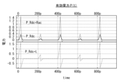
- FIG. 11 is a characteristic diagram showing the results of calculating the effective power generated in each wiring having three types of impedance characteristics.
- FIG. 12 is an explanatory diagram showing the average active power loss calculated based on the calculation results of FIG.
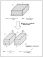
- FIG. 13 is an explanatory diagram showing an example of a method for lowering AC resistance without changing DC resistance.
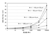
- FIG. 14 is a characteristic diagram showing the results of simulating, by electromagnetic field analysis, the frequency characteristics of resistance when the cross-sectional area of the wiring is kept constant and the ratio of the wiring width to the wiring thickness is changed.
- FIG. 15 is an explanatory diagram showing an example of DC resistance and AC resistance when a wiring is divided.
- FIG. 16 is a characteristic diagram showing the results of a simulation using electromagnetic field analysis of the resistance value per wire when a common-mode current is applied to two divided wires and the space between the wires is changed.
- FIG. 17 is a characteristic diagram showing the results of a simulation using electromagnetic field analysis of the resistance value per wire when opposite-phase currents are applied to two divided wires and the space between the wires is changed.
- FIG. 18 is a characteristic diagram showing the results of a magnetic field distribution in a cross section of the wiring when a common-mode current is passed through two divided wirings, the distribution being determined by a simulation using electromagnetic field analysis.
- FIG. 19 is a characteristic diagram showing the results of a magnetic field distribution in a cross section of the wiring when a common-mode current is passed through two divided wirings, the distribution being determined by a simulation using electromagnetic field analysis.
- FIG. 20 is a characteristic diagram showing the results of a magnetic field distribution in a cross section of the wiring when opposite-phase currents are passed through two divided wirings, the results being obtained by simulation using electromagnetic field analysis.
- FIG. 19 is a characteristic diagram showing the results of a magnetic field distribution in a cross section of the wiring when a common-mode current is passed through two divided wirings, the distribution being determined by a simulation using electromagnetic field analysis.
- FIG. 20 is a characteristic diagram showing the results of a magnetic field distribution in a cross section of the wiring when opposite-phase currents are passed through two divided wiring
- FIG. 21 is a characteristic diagram showing the results of a magnetic field distribution in a cross section of the wiring when opposite-phase currents are passed through two divided wirings, the distribution being obtained by a simulation using electromagnetic field analysis.
- FIG. 22 is a cross-sectional view showing a number of configuration examples in which the cross-sectional area of each of the two divided wirings is constant and the ratio of the wiring width to the wiring thickness is changed.
- FIG. 23 is a characteristic diagram showing the results of simulating the frequency characteristics of resistors by electromagnetic field analysis for each of the configuration examples shown in FIG. 22.
- FIG. 24 is a characteristic diagram showing the results of simulating the frequency characteristics of resistors by electromagnetic field analysis for each of the configuration examples shown in FIG. FIG.
- FIG. 25 is a configuration diagram showing an example in which a wiring is divided into four divided wirings.
- FIG. 26 is a schematic diagram showing a wiring model used for calculating the resistance.
- FIG. 27 is a characteristic diagram showing the results of calculating resistance by hand calculation and simulation by electromagnetic field analysis using the wiring model shown in FIG.
- FIG. 28 is a characteristic diagram showing the results of calculating resistance by hand calculation and simulation by electromagnetic field analysis using the wiring model shown in FIG.
- FIG. 29 is a characteristic diagram showing the results of calculating resistance by hand calculation and simulation by electromagnetic field analysis using the wiring model shown in FIG.
- FIG. 30 is an explanatory diagram showing an example of the configuration of divided wirings in which the ratio (Sp/Wd) of the inter-wiring space Sp to the individual wiring width Wd is changed.
- FIG. 31 is an explanatory diagram showing an outline of a method for calculating an optimum value of Sp/Wd for reducing AC resistance from the relationship between the number of wiring divisions, the space between wirings, the individual wiring width, and the wiring thickness.
- FIG. 32 is an explanatory diagram showing an example of calculating the number of wiring divisions and the wiring resource increase rate taking into account the wiring resource in the width direction.
- FIG. 33 is an explanatory diagram showing an example of calculating the number of wiring divisions and the wiring resource increase rate taking into account the wiring resource in the width direction.
- FIG. 34 is an explanatory diagram showing an example of the calculation result of the resistance increase rate.
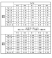
- FIG. 35 is an explanatory diagram showing an example of a calculation result of multiplying the inverse of the wiring resource increase rate by the resistance increase rate.
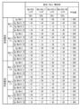
- FIG. 36 is an explanatory diagram showing an example of the relationship between the optimum number of wiring divisions N, Sp/Wd, and Wd/t values when a reverse-phase current flows.
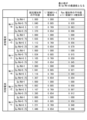
- FIG. 37 is an explanatory diagram showing an example of the relationship between the optimum number of wiring divisions N, Sp/Wd, and Wd/t values when an in-phase current flows.
- FIG. 38 is a configuration diagram showing a first example of application of wiring according to an embodiment to an electronic device.
- FIG. 39 is a configuration diagram showing a second example of application of the wiring according to the embodiment to an electronic device.
- FIG. 40 is a configuration diagram showing a third example of application of wiring according to an embodiment to an electronic device.
- FIG. 1 An example of the distribution of AC current in the vicinity of a general conductor is shown in Fig. 1.
- An example of wiring 10 made of a conductor is shown in Fig. 2.
- the vertical axis in Figure 1 indicates the electric field E.
- the electric field E is expressed as the following equation (1) in the air, and as equation (2) in a conductor.
- E0 is the amplitude constant
- j is the imaginary unit
- ⁇ is the phase constant.
- ⁇ indicates the skin depth. Note that in a conductor, current flows in the same direction as the electric field E.
- the depth (thickness) at which the current value is 1/e of the current value on the conductor surface is called the skin depth.
- the skin depth (skin thickness) ⁇ is expressed by the following equation (3).
- the parameters in equation (3) are as follows: ⁇ : Skin depth (skin thickness) (m) f: frequency of AC current (Hz) ⁇ : Conductivity of the conductor (S/m) ⁇ r: relative permeability of conductor ⁇ 0: vacuum permeability (H/m)
- Figure 3 shows an example of the relationship between skin depth ⁇ (vertical axis) and frequency f (horizontal axis) for a typical conductor.
- Figure 3 shows an example in which the conductor is copper.
- the skin depth ⁇ is on the order of ⁇ m.
- AC current only flows on the surface when it is passed through the conductor.
- the resistance of a conductor can be considered as being separated into a DC resistance Rdc and an AC resistance Rac.
- the width (wiring width) of a wiring (conductor) 10 through which a current flows is W
- the thickness (wiring thickness) of the wiring 10 is t
- the length (wiring length) of the wiring 10 is L
- Rdc (1/ ⁇ Wt) L
- Rac (1/2 ⁇ (W+t)) L
- the DC resistance Rdc is independent of the frequency f
- the AC resistance Rac is inversely proportional to the skin depth ⁇ mentioned above and increases with frequency f.
- the skin depth ⁇ decreases in proportion to the square root of the frequency f.
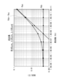
- Figure 4 shows the results of calculating the DC resistance Rdc and AC resistance Rac by hand calculation, and then calculating the sum of the DC resistance Rdc and the AC resistance Rac.
- Figure 5 shows the results of calculating the sum of the DC resistance Rdc and the AC resistance Rac by simulation using electromagnetic field analysis, compared with the results of manual calculation.
- the results of the simulation and the results of the manual calculation are approximately the same.
- Figures 6 and 7 show the calculation results when the wiring shape is changed from that of Figures 4 and 5.
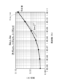
- Figures 6 and 7 show the results of calculating the DC resistance Rdc and the AC resistance Rac by manual calculation and simulation using electromagnetic field analysis.
- the results from the simulation and the results from the manual calculation are approximately the same.
- Figure 8 shows the results of comparing impedance with AC resistance Rac and L (inductance).
- FIG. 8 shows two of the three types of impedance characteristics.
- the DC resistance Rdc value of both is the same, 0.35 ⁇ .
- the frequency f at which the impedance begins to increase is almost the same.
- the increase in impedance has a characteristic that is proportional to the square root of frequency f in the Rdc + Rac characteristic, and has a characteristic that is proportional to frequency f in the Rdc + L characteristic.
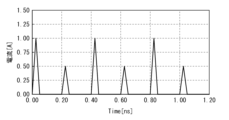
- Fig. 9 shows an example of the consumption current flowing through the wiring 10.
- Fig. 10 shows an example of the voltage drop in three types of wiring 10 having different impedance characteristics.
- the current consumption was two types,
- 1 A/25 ps and 0.5 A/25 ps, which alternated on the time axis.
- the period of the current generation was 0.4 ns, which corresponds to an operating frequency of 250 MHz.
- This current consumption was passed through the following three types of wiring 10 with different impedance characteristics.
- the voltage of characteristic 1 is V_Rdc
- the voltage of characteristic 2 is V_Rdc+Rac
- the voltage of characteristic 3 is V_Rdc+L.
- Figure 11 shows the results of calculating the active power P(t) generated in each of the wirings 10 with the above three types of impedance characteristics.
- Figure 12 shows the average loss active power P_avg calculated based on the calculation results of Figure 11.
- the active power P(t) of the above characteristic 1 is P_Rdc
- the active power P(t) of the above characteristic 2 is P_Rdc+Rac
- the active power P(t) of the above characteristic 3 is P_Rdc+L.
- the active power P(t) and the average loss active power P_avg are expressed as follows.
- P(t) re ⁇ V_R(t) x I(t) ⁇
- P_avg average(P(t))
- the real term ⁇ V_R(t) x I(t) ⁇ of the active power P(t) with respect to the power on the time axis is extracted, and the average loss active power P_avg is calculated, and the result is shown in FIG. 12.
- the AC resistance Rac causes more than twice the loss of active power P(t) compared with the DC resistance Rdc.
- the AC resistance Rac also dominates the heat generation from the conductor as the wiring 10. When operating at a high frequency f, it is very important to reduce the AC resistance Rac of the wiring 10.
- FIG. 13 shows an example of a method for lowering the AC resistance Rac without changing the DC resistance Rdc.
- the magnitude of the AC resistance Rac is greatly affected by the wiring shape.
- the cross-sectional area (W x t) can be kept constant and the surface area can be increased.
- FIG. 15 shows an example of DC resistance Rdc and AC resistance Rac when wiring 10 is divided.
- the wiring 10 may be divided into a plurality of parts as shown in FIG. 15.
- the wiring space Sp between two adjacent divided wirings is required, and therefore the wiring resource increases.
- the wiring resource refers to the wiring area for forming the wiring 10.
- the configuration example in the lower part of FIG. 15 shows a configuration example in which the wiring 10 is divided into two divided wirings 10-1 and 10-2 with the wiring space Sp between them. In the configuration example in the lower part of FIG.
- the wiring resource of the wiring 10 is increased in the width direction by the wiring space Sp compared to the wiring 10 before division.
- the DC resistance Rdc and AC resistance Rac of the divided wiring 10 are expressed as follows.
- Rdc (1/ ⁇ Wt)
- Rdc (1/ ⁇ Wt) L
- Rac (1/2 ⁇ (W+2t)) L
- the wiring width W, wiring thickness t, and number of wiring divisions N should be determined so that the following equations (4) and (5) satisfy (A+B)>(C+D). Note that in equation (5), the wiring space Sp created by the number of wiring divisions N is set to the same value as the wiring width W.
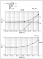
- FIG. 16 shows the results of a simulation using electromagnetic field analysis of the resistance value per wire when an in-phase current flows through the two split wires 10-1 and 10-2 and the space between the wires Sp is changed.
- FIG. 17 shows the results of a simulation using electromagnetic field analysis of the resistance value per wire when an out-of-phase current flows through the two split wires 10-1 and 10-2 and the space between the wires Sp is changed.
- the horizontal axis shows frequency f and the vertical axis shows resistance (Rdc+Rac).
- FIG. 16 and FIG. 17 show the characteristics when the wire 10 is divided into two split wires 10-1 and 10-2 with a space between the wires Sp.
- Figures 18 and 19 show the results of simulating the magnetic field distribution in the cross section of the wiring when an in-phase current is passed through the two split wirings 10-1 and 10-2, using electromagnetic field analysis.
- Figure 18 shows the results when the space between the wirings Sp is 2 ⁇ m.
- Figure 19 shows the results when the space between the wirings Sp is 40 ⁇ m.
- a reference GND ground
- Figures 20 and 21 show the results of simulating the magnetic field distribution in the cross section of the wiring when opposite-phase currents are passed through the two split wirings 10-1, 10-2, using electromagnetic field analysis.
- Figure 20 shows the results when the spacing between the wirings Sp is 2 ⁇ m.
- Figure 21 shows the results when the spacing between the wirings Sp is 40 ⁇ m.
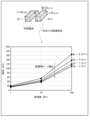
- FIGS. 23 and 24 show the results of simulating the frequency characteristics of resistance for each configuration example shown in FIG. 22 using electromagnetic field analysis.
- the horizontal axis shows frequency f
- the vertical axis shows resistance (Rdc+Rac).
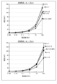
- FIG. 23 shows the results of a simulation for each configuration example shown in FIG. 22, with the inter-wire space Sp set to 5 ⁇ m, when opposite-phase currents are passed through the two split wirings 10-1 and 10-2, and when in-phase currents are passed through them.
- FIG. 24 shows the results of a simulation for each configuration example shown in FIG. 22, with the inter-wire space Sp set to 20 ⁇ m, when opposite-phase currents are passed through the two split wirings 10-1 and 10-2, and when in-phase currents are passed through them.
- the resistance of the wiring 10 is expressed as "DC resistance Rdc + AC resistance Rac.”
- the AC resistance Rac is expressed by the following formulas (6) and (7) for the cases with and without division of the wiring, where the parameters in the formulas are as follows (see FIG. 25): W: Wiring width (total width) (m) Wd: Individual wiring width of divided wiring (m) Sp: Space between wires (m) t: wiring thickness (m) L: Wiring length (m) N: Number of wiring divisions (2 or more) ⁇ : Conductivity of wiring (S/m) f: operating frequency (frequency of AC current) (GHz) A0, A1, B0, B1, C0, C1: Coefficients characterizing the wiring shape
- ⁇ (B0*(Sp/Wd) B1 *N (C0*Ln(Sp/Wd)+C1) ⁇ is a term (second term) influenced by the wiring thickness t, the wiring space Sp, and the number of wiring divisions N.
- ⁇ 1/( ⁇ *58e6) ⁇ is a term (third term) influenced by the conductivity ⁇ used for the wiring 10.
- ⁇ L/(100e-6) ⁇ is a term (fourth term) influenced by the wiring length L. Note that (Sp/Wd) is one of 1, 0.75, 0.5, and 0.25.
- A0, A1, B0, B1, C0, and C1 are fitting parameters that depend on the individual wiring width Wd and the wiring thickness t.
- Figure 26 shows a schematic of the wiring model used to calculate the resistance.
- Figures 27 to 29 show the results of calculating the resistance by hand calculation and simulation (Sim) by electromagnetic field analysis, using the wiring model shown in Figure 26.
- the horizontal axis shows the wiring width W
- FIG. 26 shows schematic diagrams of wiring models when the wiring width W is increased in the cases without and with wiring division.
- the number of wiring divisions N also increases as the wiring width W increases, and multiple divided wirings 10-1, 10-2, 10-3, ... 10-N are formed.
- Fig. 30 shows an example of the configuration of divided wiring in which the ratio (Sp/Wd) of the space between wirings Sp to the width of individual wirings Wd is changed.
- Fig. 30 shows an example in which the number of wiring divisions N is 6, and wiring 10 is configured with six divided wirings 10-1, 10-2, 10-3, 10-4, 10-5, and 10-6.
- Fig. 31 shows an overview of a method for calculating the optimal value of Sp/Wd that reduces AC resistance Rac from the relationship between the number of wiring divisions N, the space between wirings Sp, the width of individual wirings Wd, and the wiring thickness t.
- the optimum Sp/Wd for reducing the AC resistance Rac can be calculated, for example, by the following procedure. Step 1. Calculate the number of wiring divisions N, taking into account the wiring resources in the width direction, and the wiring resource increase rate. Step 2. Calculate the resistance increase rate at which Sp/Wd becomes smaller. Step 3: Taking into consideration the results of steps 1 and 2, the optimal Sp/Wd is calculated.
- the surface area also increases, so the resistance is likely to decrease. If Sp/Wd is decreased and the number of wiring divisions N is increased, the wiring resources increase, so it is not preferable to increase the number of wiring divisions N too much.
- the wiring resource increase rate in the width direction is defined as W_A/W_B, W_A/W_C, and W_A/W_D.
- the AC resistance Rac decreases as the wiring space Sp increases. Therefore, for example, as shown in Figure 31, the minimum value of the product of the inverse of the wiring resource increase rate (1/wiring resource increase rate) for each value of Sp/Wd and the resistance increase rate is set to the optimal value of Sp/Wd.
- Figures 32 and 33 show examples of calculating the number of wiring divisions N and the wiring resource increase rate taking into account the width-wise wiring resources according to step 1 above.
- the wiring resource increase rate is defined as W_A ⁇ W_B.
- Figure 33 shows the wiring resource increase rate when the number of wiring divisions N is increased.
- the number of wiring divisions N is 4 or more, and preferably the number of wiring divisions N is 5 or more.
- Figure 34 shows an example of the calculation result of the resistance increase rate according to step 2 above.
- Figure 35 shows an example of the calculation result of multiplying the inverse of the wiring resource increase rate (1/wiring resource increase rate) by the resistance increase rate according to step 3 above.
- the minimum value of the result of multiplying the inverse of the wiring resource increase rate by the resistance increase rate is set as the optimal value of Sp/Wd.
- the frequency f is 1 GHz, but since the resistance (Rdc + Rac) is proportional to the square root of the frequency f when calculating the optimal value of Sp/Wd, the frequency f can be any value.
- XXX is, for example, 40 ⁇ m.
- the minimum value of the result of multiplying the reciprocal of the wiring resource increase rate by the resistance increase rate is the value that can reduce the AC resistance Rac, so the Sp/Wd value corresponding to this minimum value is the desired value of Sp/Wd.
- Figure 36 shows an example of the relationship between the optimal number of wiring divisions N, Sp/Wd, and Wd/t when a reverse-phase current flows.
- Figure 37 shows an example of the relationship between the optimal number of wiring divisions N, Sp/Wd, and Wd/t when a common-phase current flows.
- the individual wiring width Wd is set to an arbitrary value. From the results thus far and the results of Figures 36 and 37, in terms of both the wiring resource and the rate of increase in resistance, in order to efficiently reduce the AC resistance Rac caused by the skin effect, it is desirable that the wiring 10 be divided so as to satisfy the following condition.
- the individual wiring width Wd is set to an arbitrary value.
- N 4 or more (preferably 5 or more) Wd/t: 0.5 to 6 Sp/Wd: When a reverse-phase current is applied, it is 0.2 to 0.55. 0.35 to 0.95 when in-phase current flows
- Wd/t may be the following value.
- Wd/t 1 or less.
- Wd/t 1 or more.
- the wiring 10 according to the embodiment is applicable to various electronic devices.
- the wiring 10 according to the embodiment is applicable to all substrates on which the divided wiring 10 can be formed.
- the wiring 10 according to the embodiment is applicable to printed circuit boards (PCBs), packages of electronic components and semiconductors, and semiconductor chips.
- the wiring 10 is also applicable to wiring 10 through which a reverse-phase current or a common-phase current flows as an AC current.
- the wiring 10 is also applicable to signal wiring that transmits a data signal or a clock signal.
- the wiring 10 is also applicable to power supply wiring and GND (ground) wiring.
- the divided wiring 10 can also be formed on either a surface layer or an inner layer.
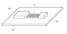
- FIG. 38 shows a first example of application of wiring according to one embodiment to electronic equipment.
- FIG. 38 shows an example in which divided wiring 10 is applied to a printed circuit board (PCB) 101.
- the divided wiring 10 according to the technology of one embodiment can be applied as a connection wiring between a package 102 having a semiconductor chip or the like built in on the printed circuit board (PCB) 101 and components such as a package or a connector.
- FIG. 39 shows a second example of application of wiring according to one embodiment to electronic equipment.
- FIG. 39 shows an example in which divided wiring 10 is applied to a package substrate 111.
- a semiconductor chip 112 is fixed onto the package substrate 111 by, for example, a bonding wire 113.
- the divided wiring 10 according to the technology of one embodiment can be applied as a connection wiring between the semiconductor chip 112 and a package output terminal 114.
- Figure 40 shows a third example of application of wiring according to one embodiment to electronic equipment.
- FIG. 40 shows an example in which divided wiring 10 is applied to a semiconductor chip 121.
- the semiconductor chip 121 is provided with a semiconductor circuit 124 that consumes power supply or GND (ground) current.
- the semiconductor circuit 124 is connected to a power supply wiring or GND wiring 122.
- the power supply wiring or GND wiring 122 is connected to a bonding wire 123.
- the wiring 10 divided by the technology according to one embodiment can be applied as the power supply wiring or GND wiring 122.
- the semiconductor chip 121 is also provided with a transmission buffer 126 that transmits a clock signal or a data signal, and a reception buffer 127 that receives a clock signal or a data signal.
- the transmission buffer 126 and the reception buffer 127 are connected to each other by a signal wiring 125.
- the signal wiring 125 can be the wiring 10 divided by the technology according to one embodiment.
- the wiring 10 is made up of a plurality of divided wirings, and the divided wirings are optimized so as to reduce the increase in resistance due to the skin effect, thereby making it possible to reduce the increase in resistance in the high frequency region due to the skin effect.
- the increase in resistance in the high frequency range due to the skin effect can be suppressed by dividing the wiring 10 into multiple parts to increase the surface area.
- the increase in resistance in the high frequency range can be sufficiently suppressed by optimizing the configuration parameters when dividing the wiring 10 into multiple parts, such as the number of wiring divisions N, the individual wiring width Wd of the divided wiring 10, and the space between the wirings Sp.
- the present technology can be configured as follows.
- the wiring is composed of a plurality of divided wirings, and the divided wirings are optimized to reduce the increase in resistance due to the skin effect, thereby making it possible to reduce the increase in resistance in the high frequency region due to the skin effect.
- the plurality of divided wirings include The number of wiring divisions is set to 4 or more, When the space between two adjacent divided wirings is Sp and the individual wiring width of each of the divided wirings is Wd, When a reverse-phase current is passed through the plurality of divided wirings as the AC current, Sp/Wd is 0.2 or more and 0.55 or less, The wiring is configured so that Sp/Wd satisfies 0.35 to 0.95 when an in-phase current is passed through the plurality of divided wirings as the AC current.
- a common-mode current is caused to flow through the plurality of divided wirings as the AC current,
- the individual wiring width of each of the plurality of divided wirings is Wd and the wiring thickness of each of the plurality of divided wirings is t
- the wiring according to (1) or (2) above, configured to satisfy Wd/t being 1 or more.
- the number of wiring divisions is calculated based on a calculation formula for AC resistance that includes terms influenced by the wiring thickness of each of the multiple divided wirings, the space between the wirings, and the frequency of the AC current, and terms influenced by the wiring thickness, the space between the wirings, and the number of wiring divisions.
- each of the plurality of divided wirings has a wiring length of 100 ⁇ m or more.
- the wiring according to any one of (1) to (6) above, wherein the plurality of divided wirings are used as signal wirings.
- the wiring according to any one of (1) to (6) above, wherein the plurality of divided wirings are used as power supply wirings.
- the wiring according to any one of (1) to (6) above, wherein the plurality of divided wirings are used as ground wiring.
- a wiring including a plurality of divided wirings through which an AC current flows The plurality of divided wirings include The number of wiring divisions is set to 4 or more, When the space between two adjacent divided wirings is Sp and the individual wiring width of each of the divided wirings is Wd, When a reverse-phase current is passed through the plurality of divided wirings as the AC current, Sp/Wd is 0.2 or more and 0.55 or less, The electronic device is configured so that Sp/Wd satisfies 0.35 to 0.95 when an in-phase current is caused to flow as the AC current through the plurality of divided wirings.
Landscapes
- Structure Of Printed Boards (AREA)
Abstract
本開示の配線は、それぞれに交流電流が流れる複数の分割配線からなり、複数の分割配線は、配線分割数が4以上とされ、隣り合う2つの分割配線同士の配線間スペースをSp、複数の分割配線のそれぞれの個別配線幅をWdとしたとき、複数の分割配線に交流電流として逆相電流を流す場合にはSp/Wdが0.2以上0.55以下、複数の分割配線に交流電流として同相電流を流す場合にはSp/Wdが0.35以上0.95以下を満たすように構成されている。
Description
本開示は、配線、および電子機器に関する。
銅などの配線は、流れる電流の周波数が高くなると配線表面に電流が集中するため抵抗が高くなる。これは表皮効果と呼ばれている。高周波電流が流れる配線の抵抗を低くする技術として、配線を複数に分割する構成が提案されている(特許文献1参照)。
表皮効果により抵抗が高くなると、損失有効電力の増大による発熱や、電圧降下を招く。特許文献1に記載の技術では、配線を複数に分割する際の構成パラメータ、例えば、配線分割数や配線幅、および配線間スペースなどの最適化が十分になされておらず、高周波領域における抵抗増加の抑制効果が不十分である。
表皮効果による高周波領域における抵抗増加を低減することが可能な配線、および電子機器を提供することが望ましい。
本開示の一実施の形態に係る配線は、それぞれに交流電流が流れる複数の分割配線からなり、複数の分割配線は、配線分割数が4以上とされ、隣り合う2つの分割配線同士の配線間スペースをSp、複数の分割配線のそれぞれの個別配線幅をWdとしたとき、複数の分割配線に交流電流として逆相電流を流す場合にはSp/Wdが0.2以上0.55以下、複数の分割配線に交流電流として同相電流を流す場合にはSp/Wdが0.35以上0.95以下を満たすように構成されている。
本開示の一実施の形態に係る電子機器は、それぞれに交流電流が流れる複数の分割配線からなる配線を有し、複数の分割配線は、配線分割数が4以上とされ、隣り合う2つの分割配線同士の配線間スペースをSp、複数の分割配線のそれぞれの個別配線幅をWdとしたとき、複数の分割配線に交流電流として逆相電流を流す場合にはSp/Wdが0.2以上0.55以下、複数の分割配線に交流電流として同相電流を流す場合にはSp/Wdが0.35以上0.95以下を満たすように構成されている。
本開示の一実施の形態に係る配線、または電子機器では、表皮効果による抵抗増加を低減することが可能となるように、複数の分割配線が最適化されている。
以下、本開示の実施の形態について図面を参照して詳細に説明する。なお、説明は以下の順序で行う。
1.一実施の形態
1.1 背景(図1~図12)
1.2 表皮効果を考慮した配線構造(図13~図37)
1.2.1 交流抵抗を下げる方法
1.2.2 配線間スペースを考慮した交流抵抗の算出式
1.2.3 効率よく配線分割数を決める方法
1.3 適用例(図38~図40)
1.4 効果
2.その他の実施の形態
1.一実施の形態
1.1 背景(図1~図12)
1.2 表皮効果を考慮した配線構造(図13~図37)
1.2.1 交流抵抗を下げる方法
1.2.2 配線間スペースを考慮した交流抵抗の算出式
1.2.3 効率よく配線分割数を決める方法
1.3 適用例(図38~図40)
1.4 効果
2.その他の実施の形態
<1.一実施の形態>
[1.1 背景]
[1.1 背景]
(表皮効果について)
図1に、一般的な導体近傍における交流電流の分布の一例を示す。図2に、導体からなる配線10の一例を示す。
図1に、一般的な導体近傍における交流電流の分布の一例を示す。図2に、導体からなる配線10の一例を示す。
図1の横軸は導体表面を基準位置(Z=0)とした導体表面からの位置Zを示す。図1の縦軸は電界Eを示す。電界Eは空気中では以下の式(1)のように表され、導体中では式(2)のように表される。E0は振幅定数、jは虚数単位、βは位相定数とする。δは表皮深さ(表皮厚)を示す。なお、導体では電界Eと同じ方向に電流が流れる。導体表面の電流値に対して電流値が1/eとなる深さ(厚さ)を表皮深さ(表皮厚)という。


導体に交流電流を流すと、表皮効果という現象が生じる。表皮効果により、交流電流の周波数fが高くなると導体の表面に電流が集中する。これにより、周波数fが高くなると導体の交流抵抗は大きくなる。表皮深さ(表皮厚)δは、以下の式(3)のように表される。
式(3)の各パラメータは以下を表す。
δ:表皮深さ(表皮厚)(m)
f:交流電流の周波数(Hz)
σ:導体の導電率(S/m)
μr:導体の比透磁率
μ0:真空透磁率(H/m)
式(3)の各パラメータは以下を表す。
δ:表皮深さ(表皮厚)(m)
f:交流電流の周波数(Hz)
σ:導体の導電率(S/m)
μr:導体の比透磁率
μ0:真空透磁率(H/m)

図3に、一般的な導体における表皮深さδ(縦軸)と周波数f(横軸)との関係の一例を示す。
図3は導体を銅(Copper)とした場合の例となる。交流電流の周波数fが1GHzを超えると、表皮深さδはμmオーダーとなる。周波数fが高くなると、導体に交流電流を流しても表面にしか交流電流は流れない。
(導体の抵抗について)
導体の抵抗は直流抵抗Rdcと交流抵抗Racとに分離して考えることができる。図2に示したように、電流が流れる配線(導体)10の幅(配線幅)をW、配線10の厚み(配線厚)をt、配線10の長さ(配線長)をLとすると、直流抵抗Rdcと交流抵抗Racは以下のように表される。
Rdc=(1/σWt)・L
Rac=(1/2σδ(W+t))・L
導体の抵抗は直流抵抗Rdcと交流抵抗Racとに分離して考えることができる。図2に示したように、電流が流れる配線(導体)10の幅(配線幅)をW、配線10の厚み(配線厚)をt、配線10の長さ(配線長)をLとすると、直流抵抗Rdcと交流抵抗Racは以下のように表される。
Rdc=(1/σWt)・L
Rac=(1/2σδ(W+t))・L
直流抵抗Rdcは周波数fとは無関係のものとなり、交流抵抗Racは前述した表皮深さδに反比例し周波数fと共に大きくなる。表皮深さδは、図3からも分かるように、周波数fの平方根に比例して小さくなる。
図4に、手計算により直流抵抗Rdcと交流抵抗Racとを算出し、さらに直流抵抗Rdcと交流抵抗Racとの和を算出した結果を示す。図5に、電磁界解析によるシミュレーションによって直流抵抗Rdcと交流抵抗Racとの和を算出した結果を、手計算による結果と比較したものを示す。図4および図5には、配線10の導体材料としては銅を使用し、配線形状を配線幅W=40μm、配線厚t=20μm、配線長L=100μmとした結果を示す。図5から分かるように、シミュレーションによる結果と手計算による結果は略一致する。
図6および図7に、図4および図5とは配線形状を変えた場合の計算結果を示す。図6および図7には、直流抵抗Rdcと交流抵抗Racとを手計算と電磁界解析によるシミュレーションとによって算出した結果を示す。図6には、配線10の導体材料としては銅を使用し、配線形状を配線幅W=5μm、配線厚t=5μm、配線長L=100μmとした結果を示す。図7には、配線10の導体材料としては銅を使用し、配線形状を配線幅W=1μm、配線厚t=1μm、配線長L=100μmとした結果を示す。図6および図7からも分かるように、配線形状を変えた場合においても、シミュレーションによる結果と手計算による結果は略一致している。
図8に、インピーダンスを交流抵抗RacとL(インダクタンス)とで比較した結果を示す。
交流抵抗Racによる影響を確認するため、配線10として、3種類のインピーダンス特性を有するものを用い、各インピーダンス特性の配線10に電流を流し、シミュレーションにより電力計算を行った(後述の図11)。図8には、3種類のうち2つのインピーダンス特性を示す。1つは直流抵抗Rdcと交流抵抗Racとの和(Rdc+Rac)となるインピーダンス特性で、配線幅W=20μm、配線厚t=2μm、配線長L=1000μmの配線10に相当する抵抗特性を持つ。もう1つは、直流抵抗RdcとインダクタンスLとの和(Rdc+L)となるインピーダンス特性で、インダクタンスLの値はL=33pHとした。両者の直流抵抗Rdcの値は同じであり、0.35Ωとした。両者の特性共に、インピーダンスが増加し始める周波数fはほぼ同じとなる。インピーダンスの増加は、Rdc+Racの特性では周波数fの平方根に比例する特性を持ち、Rdc+Lの特性では周波数fに比例する特性を持つ。
(電流と電圧降下について)
図9に、配線10に流す消費電流の一例を示す。図10は、異なるインピーダンス特性を持つ3種類の配線10の電圧降下の一例を示す。
図9に、配線10に流す消費電流の一例を示す。図10は、異なるインピーダンス特性を持つ3種類の配線10の電圧降下の一例を示す。
図9に示したように、消費電流は時間軸上において、|di/dt|=1A/25ps,0.5A/25psの2種類が交互に発生するものを使用した。電流発生の周期は0.4nsであり、250MHzの動作周波数に相当する。この消費電流を、異なるインピーダンス特性を持つ以下の3種類の配線10に流した。図10に示したように、特性1の電圧をV_Rdc、特性2の電圧をV_Rdc+Rac、特性3の電圧をV_Rdc+Lとする。
特性1:Rdcのみ
特性2:Rdc+Rac
特性3:Rdc+L
特性1:Rdcのみ
特性2:Rdc+Rac
特性3:Rdc+L
上記各特性の配線10の両端に発生する電圧をシミュレーションし、モニタした。図10に示したように、上記各特性の電圧降下の大小関係は以下のようになった。高周波帯における動作では抵抗による電圧降下は、直流抵抗Rdcより交流抵抗Racの方が著しく大きい。
(特性3)>(特性2)>(特性1)
(特性3)>(特性2)>(特性1)
図11に、上記3種類のインピーダンス特性の各配線10のそれぞれに生じる有効電力P(t)を算出した結果を示す。図12は、図11の算出結果に基づいて算出された平均損失有効電力P_avgを示す。上記特性1の有効電力P(t)をP_Rdc、上記特性2の有効電力P(t)をP_Rdc+Rac、上記特性3の有効電力P(t)をP_Rdc+Lとする。
有効電力P(t)、平均損失有効電力P_avgは以下で表される。
P(t)=re{V_R(t)×I(t)}
P_avg=average(P(t))
時間軸上の電力に対して有効電力P(t)の実部項{V_R(t)×I(t)}を抜き出し、平均損失有効電力P_avgを求めた結果を図12に示す。直流抵抗Rdcよりも交流抵抗Racの方が2倍以上の有効電力P(t)の損失を生じさせる。そして、配線10としての導体からの発熱も交流抵抗Racが支配的となる。高い周波数fで動作させる場合、配線10の交流抵抗Racを低減させることがとても重要となる。
P(t)=re{V_R(t)×I(t)}
P_avg=average(P(t))
時間軸上の電力に対して有効電力P(t)の実部項{V_R(t)×I(t)}を抜き出し、平均損失有効電力P_avgを求めた結果を図12に示す。直流抵抗Rdcよりも交流抵抗Racの方が2倍以上の有効電力P(t)の損失を生じさせる。そして、配線10としての導体からの発熱も交流抵抗Racが支配的となる。高い周波数fで動作させる場合、配線10の交流抵抗Racを低減させることがとても重要となる。
[1.2 表皮効果を考慮した配線構造]
(1.2.1 交流抵抗を下げる方法)
図13に、直流抵抗Rdcを変化させずに交流抵抗Racを下げる方法の一例を示す。
(1.2.1 交流抵抗を下げる方法)
図13に、直流抵抗Rdcを変化させずに交流抵抗Racを下げる方法の一例を示す。
上述したように、配線幅をW、配線厚をt、配線長をL、表皮深さをδ、配線(導体)10の導電率をσとすると、直流抵抗Rdcと交流抵抗Racは以下のように表される。
Rdc=(1/σWt)・L
Rac=(1/2σδ(W+t))・L
Rdc=(1/σWt)・L
Rac=(1/2σδ(W+t))・L
交流抵抗Racの大きさはその配線形状に大きく左右される。直流抵抗Rdcを変化させずに交流抵抗Racを下げるには、例えば図13に示したように、断面積(W×t)を一定とし、表面積を大きくすればよい。
図14に、配線10の断面積(W×t)を一定(W×t=800(μm2))とし、配線幅Wと配線厚tの比を変えた場合の抵抗の周波数特性をシミュレーションした結果を示す。横軸は周波数f、縦軸は抵抗(Rdc+Rac)を示す。
図14の結果より、表面積を増やすように配線形状を工夫すれば交流抵抗Racを小さくすることが可能となることが分かる。
図15に、配線10を分割した場合の直流抵抗Rdcおよび交流抵抗Racの一例を示す。
上述したように、配線10の断面積(W×t)を一定としつつ表面積を増加させるには、図15に示したように、配線10を複数に分割すればよい。ただし、配線10を複数に分割すると、隣り合う2つの分割配線同士の配線間スペースSpが必要となるため、配線リソースが増加する。ここで、配線リソースとは、配線10を構成するための配線領域のことをいう。図15の下段の構成例では、配線間スペースSpを空けて配線10を2つの分割配線10-1,10-2に分割した構成例を示している。図15の下段の構成例では、2つの分割配線10-1,10-2のそれぞれの個別配線幅Wdを、図15の上段に示した分割前の配線10の配線幅Wの1/2としている(Wd=W/2)。図15の下段の構成例では、分割前の配線10に対し、配線間スペースSp分、幅方向に配線10の配線リソースが増加している。この場合、分割後の配線10の直流抵抗Rdcと交流抵抗Racは以下のように表される。
Rdc=(1/σWt)・L
Rac=(1/2σδ(W+2t))・L
Rdc=(1/σWt)・L
Rac=(1/2σδ(W+2t))・L
幅方向の配線リソースをできるだけ増加させずに交流抵抗Racを下げるには、理論上、以下の式(4),(5)に関し、(A+B)>(C+D)が満たせるように配線幅W、配線厚t、配線分割数Nを決めればよい。なお、式(5)において、配線分割数Nによって生じる配線間スペースSpは配線幅Wと同じ値にした。
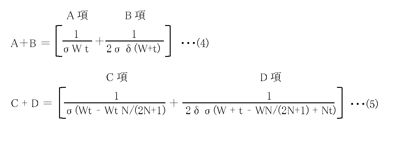
図16に、2つの分割配線10-1,10-2に同相電流を流し、配線間スペースSpを変えた場合の配線1本辺りの抵抗値を電磁界解析によるシミュレーションにより求めた結果を示す。図17に、2つの分割配線10-1,10-2に逆相電流を流し、配線間スペースSpを変えた場合の配線1本辺りの抵抗値を電磁界解析によるシミュレーションにより求めた結果を示す。図16および図17において、横軸は周波数f、縦軸は抵抗(Rdc+Rac)を示す。図16および図17には、配線間スペースSpを空けて、配線10を2つの分割配線10-1,10-2に分割した場合の特性を示す。図16および図17には、分割配線10-1,10-2の導体材料としては銅を使用し、配線形状を配線幅Wd=20μm、配線厚t=20μm、配線長L=100μmとした結果を示す。
上述の(A+B)>(C+D)の数式は配線10を分割した際の配線間スペースSpに交流抵抗Racが依存しない前提だと成り立つが、実際はそうではない。分割したことによって生じる配線間スペースSpを増加させると、交流抵抗Racは減少する傾向にある。
図18および図19に、2つの分割配線10-1,10-2に同相電流を流した場合の配線断面の磁界分布を電磁界解析によるシミュレーションにより求めた結果を示す。図18には配線間スペースSpが2μmの場合の結果を示す。図19には配線間スペースSpが40μmの場合の結果を示す。シミュレーションでは、リファレンスGND(グランド)を配線直下300μmに配置した。そのGND(グランド)上に配線幅Wd=20μm,配線厚t=20μmの2本の分割配線10-1,10-2を配置し、励振源を交流電圧AC=1Vの電位差、周波数f=10GHzとして同相電流を与えた。
2つの分割配線10-1,10-2に同相電流を流した場合、互いの配線で生じる磁界が打ち消し合う。2つの分割配線10-1,10-2が近接すると磁界の打ち消し効果が顕著になり、分割配線10-1,10-2の隣接面には電流が流れにくくなる。図18に示したように配線間スペースSpが小さいと配線間には磁場が少なくなり、表面電流の面積は小さくなる。結果として抵抗が大きくなる。逆に、図19に示したように配線間スペースSpを大きくするとこの現象は緩和され、配線間には磁場が多くなり、表面電流の面積は大きくなる。結果として、抵抗は小さくなる。
図20および図21に、2つの分割配線10-1,10-2に逆相電流を流した場合の配線断面の磁界分布を電磁界解析によるシミュレーションにより求めた結果を示す。図20には配線間スペースSpが2μmの場合の結果を示す。図21には配線間スペースSpが40μmの場合の結果を示す。シミュレーションでは、配線幅Wd=20μm,配線厚t=20μmの2本の分割配線10-1,10-2を配置し、励振源を交流電圧AC=1Vの電位差、周波数f=10GHzとして逆相電流を与えた。
逆相電流を流した場合、2つの分割配線10-1,10-2が近接すると帰路電流の近接化により電磁界が閉じ込められ電磁界の広がりが小さくなり、分割配線10-1,10-2に流れる電流により生じる磁界は配線間にて強め合う方向に働く。故に、図20に示したように配線間スペースSpが小さいと、配線間に磁場が集中し、ほとんど、ここにしか電流が流れなくなる。これにより、配線表面に浸透する磁場が少なくなり、表面電流の面積は小さくなる。結果として、抵抗が大きくなる。逆に、図21に示したように配線間スペースSpを大きくするとこの現象は緩和され、配線表面に浸透する磁場が多くなり、表面電流の面積は大きくなる。結果として、抵抗は小さくなる。
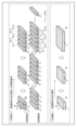
図22に、2つの分割配線10-1,10-2のそれぞれの断面積(Wd×t)を一定(Wd×t=400μm2)とし、配線幅(個別配線幅Wd)と配線厚tとの比(Wd/t)を変えた複数の構成例を示す。図22には、複数の構成例として、Wd=5μm,t=80μm(図22の(A))、Wd=10μm,t=40μm(図22の(B))、Wd=20μm,t=20μm(図22の(C))、Wd=40μm,t=10μm(図22の(D))、Wd=80μm,t=5μm(図22の(E))とした構成例を示す。
図23および図24に、図22に示した各構成例について、抵抗の周波数特性を電磁界解析によりシミュレーションした結果を示す。図23および図24において、横軸は周波数f、縦軸は抵抗(Rdc+Rac)を示す。図23には、図22に示した各構成例について、配線間スペースSpを5μmとし、2つの分割配線10-1,10-2に逆相電流を流した場合と同相電流を流した場合とのシミュレーション結果を示す。図24には、図22に示した各構成例について、配線間スペースSpを20μmとし、2つの分割配線10-1,10-2に逆相電流を流した場合と同相電流を流した場合とのシミュレーション結果を示す。
図23および図24の結果から、配線間の結合面積(Sp×t)が大きくなる(Wd/tが小さくなる)と、逆相電流を流した場合の配線抵抗は小さくなる傾向になることが分かる。逆に、配線間の結合面積(Sp×t)が小さくなる(Wd/tが大きくなる)と、同相電流を流した場合の配線抵抗は小さくなる傾向になることが分かる。図23および図24の結果は、図18~図21を用いて説明した理論と特性の傾向が一致する。
以上の結果から、後述する配線リソースや配線間スペースSpを考慮しない場合、逆相電流を流す場合、例えばWd/t=1以下で構成することが望ましい。また、同相電流を流す場合、例えばWd/t=1以上で構成することが望ましい。
(1.2.2 配線間スペースを考慮した交流抵抗の算出式)
図25に、配線10を4つの分割配線10-1,10-2,10-3,10-4に分割した構成例を示す(配線分割数N=4)。
図25に、配線10を4つの分割配線10-1,10-2,10-3,10-4に分割した構成例を示す(配線分割数N=4)。
配線10の抵抗は、「直流抵抗Rdc+交流抵抗Rac」で表される。直流抵抗Rdcは、以下で表される。
Rdc=(1/σWt)・L
Rdc=(1/σWt)・L
交流抵抗Racは、配線分割が無い場合と有る場合とで以下の式(6),(7)で表される。なお、式中のパラメータは以下のとおりである(図25参照)。
W:配線幅(全体の幅)(m)
Wd:分割配線の個別配線幅(m)
Sp:配線間スペース(m)
t:配線厚(m)
L:配線長(m)
N:配線分割数(2以上)
σ:配線の導電率(S/m)
f:動作周波数(交流電流の周波数)(GHz)
A0,A1,B0,B1,C0,C1:配線形状に特徴づけられる係数
W:配線幅(全体の幅)(m)
Wd:分割配線の個別配線幅(m)
Sp:配線間スペース(m)
t:配線厚(m)
L:配線長(m)
N:配線分割数(2以上)
σ:配線の導電率(S/m)
f:動作周波数(交流電流の周波数)(GHz)
A0,A1,B0,B1,C0,C1:配線形状に特徴づけられる係数
<配線分割無し>
Rac={(A0*(√f)}*{(B0*WB1)}*{1/(σ*58e6)}*{L/(100e-6)} ……(6)
ここで、(A0*(√f)は、配線厚tと配線幅Wと周波数fとが影響を与える項である。(B0*WB1)は、配線厚tと配線幅Wとが影響を与える項である。1/(σ*58e6)は、配線10に使用する導電率σが影響を与える項である。L/(100e-6)は、配線長Lが影響を与える項である。
Rac={(A0*(√f)}*{(B0*WB1)}*{1/(σ*58e6)}*{L/(100e-6)} ……(6)
ここで、(A0*(√f)は、配線厚tと配線幅Wと周波数fとが影響を与える項である。(B0*WB1)は、配線厚tと配線幅Wとが影響を与える項である。1/(σ*58e6)は、配線10に使用する導電率σが影響を与える項である。L/(100e-6)は、配線長Lが影響を与える項である。
<配線分割有り>
Rac={(A0*Ln(Sp/Wd)+A1)*(√f)}*{(B0*(Sp/Wd)B1*N(C0*Ln(Sp/Wd)+C1)}*{1/(σ*58e6)}*{L/(100e-6)}*0.5 ……(7)
ここで、{(A0*Ln(Sp/Wd)+A1)*(√f)}は、配線厚tと配線間スペースSpと周波数fとが影響を与える項(第1項)である。{(B0*(Sp/Wd)B1*N(C0*Ln(Sp/Wd)+C1)}は、配線厚tと配線間スペースSpと配線分割数Nとが影響を与える項(第2項)である。{1/(σ*58e6)}は、配線10に使用する導電率σが影響を与える項(第3項)である。{L/(100e-6)}は、配線長Lが影響を与える項(第4項)である。なお、(Sp/Wd)は、1,0.75,0.5,0.25のいずれかを使用する。A0,A1,B0,B1,C0,C1は、個別配線幅Wdと配線厚tとに依存したフィッティングパラメータである。
Rac={(A0*Ln(Sp/Wd)+A1)*(√f)}*{(B0*(Sp/Wd)B1*N(C0*Ln(Sp/Wd)+C1)}*{1/(σ*58e6)}*{L/(100e-6)}*0.5 ……(7)
ここで、{(A0*Ln(Sp/Wd)+A1)*(√f)}は、配線厚tと配線間スペースSpと周波数fとが影響を与える項(第1項)である。{(B0*(Sp/Wd)B1*N(C0*Ln(Sp/Wd)+C1)}は、配線厚tと配線間スペースSpと配線分割数Nとが影響を与える項(第2項)である。{1/(σ*58e6)}は、配線10に使用する導電率σが影響を与える項(第3項)である。{L/(100e-6)}は、配線長Lが影響を与える項(第4項)である。なお、(Sp/Wd)は、1,0.75,0.5,0.25のいずれかを使用する。A0,A1,B0,B1,C0,C1は、個別配線幅Wdと配線厚tとに依存したフィッティングパラメータである。
配線分割が有った場合、交流抵抗Racについては配線間スペースSpの影響を考慮する必要があると前述した。式(7)では、第1項と第2項とを数式に組み込むことでこれを考慮できている。式(7)に基づいて、抵抗値が小さくなるような配線分割数N等を求めることができる。
上述の式(6),(7)で算出される抵抗の妥当性を確認するため、配線モデルを作成し、手計算と電磁界解析によるシミュレーションとによって抵抗を算出して比較を行った。図26に、抵抗の算出に用いた配線モデルを概略的に示す。図27ないし図29に、図26に示した配線モデルを用いて、手計算と電磁界解析によるシミュレーション(Sim)とによって抵抗を算出した結果を示す。図27ないし図29において、横軸は配線幅W、縦軸は抵抗R(=Rdc+Rac)を示す。
配線モデルとしては、配線分割無しの場合と配線分割有りの場合とを作成し、同相電流と逆相電流とを流した場合について抵抗を算出した。図26には、配線分割無しの場合と配線分割有りの場合において、配線幅Wを増加させた場合の配線モデルを模式的に示す。配線分割有りの場合、配線幅Wの増加に伴い、配線分割数Nも増加し、複数の分割配線10-1,10-2,10-3,…10-Nが形成される。
配線10には、交流電圧AC=1Vの電位差を与え、総電流から抵抗を算出した。配線分割有りの場合、抵抗R(=Rdc+Rac)は以下で表される。同相電流をIc、逆相電流はIf,Ir、配線分割無しの電流はIとする。
同相電流:R=V/ΣIc
逆相電流:R=V/ΣIf(Irの電流値は非対象とし、Wd+Spは同相電流と同じものを使用)
配線分割無しの場合、抵抗R(=Rdc+Rac)は以下で表される。
R=V/I
同相電流:R=V/ΣIc
逆相電流:R=V/ΣIf(Irの電流値は非対象とし、Wd+Spは同相電流と同じものを使用)
配線分割無しの場合、抵抗R(=Rdc+Rac)は以下で表される。
R=V/I
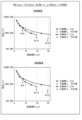
図27には、配線形状として、個別配線幅Wd=40μm,配線厚t=40μm,配線間スペースSpと個別配線幅Wdとの比Sp/Wd=0.5,配線長L=100μmとし、周波数f=10GHzとした場合の算出結果を示す。図28には、配線形状として、個別配線幅Wd=5μm,配線厚t=2.5μm,Sp/Wd=1,配線長L=100μmとし、周波数f=10GHzとした場合の算出結果を示す。図29には、配線形状として、個別配線幅Wd=1μm,配線厚t=0.25μm,Sp/Wd=1,配線長L=100μmとし、周波数f=100GHzとした場合の算出結果を示す。
図27ないし図29に示したように、手計算による結果と電磁界解析によるシミュレーションによる結果は、ほぼ同じ値を示す。なお、図27ないし図29のケースでは配線分割有りの方が、配線分割無しの場合よりも小さい値を示すような条件(配線モデルや動作周波数)を使用したが、条件によっては、分割無しの方が抵抗が小さくなるケースもある。なお、ここでは、Sp/Wdを、1,0.75,0.5,0.25としてA0,A1,B0,B1,C0,C1なるフィッティングパラメータの値を使用した計算例を示したが、Sp/Wdを任意の値として計算することも可能である。
(1.2.3 効率よく配線分割数を決める方法)
図30に、配線間スペースSpと個別配線幅Wdとの比(Sp/Wd)を変えた分割配線の構成例を示す。図30には、配線分割数N=6とし、配線10を6つの分割配線10-1,10-2,10-3,10-4,10-5,10-6で構成した例を示す。図31には、配線分割数Nと配線間スペースSpと個別配線幅Wdと配線厚tとの関係から、交流抵抗Racを小さくする最適なSp/Wdの値を算出する手法の概要を示す。
図30に、配線間スペースSpと個別配線幅Wdとの比(Sp/Wd)を変えた分割配線の構成例を示す。図30には、配線分割数N=6とし、配線10を6つの分割配線10-1,10-2,10-3,10-4,10-5,10-6で構成した例を示す。図31には、配線分割数Nと配線間スペースSpと個別配線幅Wdと配線厚tとの関係から、交流抵抗Racを小さくする最適なSp/Wdの値を算出する手法の概要を示す。
交流抵抗Racを小さくする最適なSp/Wdは、例えば以下の手順で算出することができる。
手順1.幅方向の配線リソースを考慮した配線分割数N、および配線リソース増加率を算出する。
手順2. Sp/Wdが小さくなる抵抗増加率を算出する。
手順3. 手順1.手順2.の結果を考慮し、最適なSp/Wdを算出する。
手順1.幅方向の配線リソースを考慮した配線分割数N、および配線リソース増加率を算出する。
手順2. Sp/Wdが小さくなる抵抗増加率を算出する。
手順3. 手順1.手順2.の結果を考慮し、最適なSp/Wdを算出する。
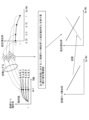
Sp/Wdが大きい方が、交流抵抗は小さくなる。一方、配線分割数Nを増加することでも表面積が増加するので抵抗は下がり易い。Sp/Wdを小さくし、配線分割数Nを増やすと配線リソースは増加するので、配線分割数Nを増やしすぎるのも好ましくない。ここで、図30に示したように、Sp/Wd=1のときの配線10の全体の幅をW_A、Sp/Wd=0.75のときの配線10の全体の幅をW_B、Sp/Wd=0.5のときの配線10の全体の幅をW_C、Sp/Wd=0.25のときの配線10の全体の幅をW_Dとする。この場合、幅方向の配線リソース増加率をW_A/W_B、W_A/W_C、W_A/W_Dのように定義する。図31に示したように、配線分割数Nを増加した場合、配線リソース増加率は飽和して一定値に落ち着く。飽和に近づく配線分割数Nが配線リソースに対する効率が大きいと言える。図31の例では、例えば、N=7で飽和する。また例えば配線リソース増加率はW_A/W_D=1.5で飽和する。W_Dの構成の場合、あまり配線リソースを消費していない一方で、配線間スペースSpは小さいので交流抵抗Racは増える。配線分割数Nと配線リソース増加率との関係では、配線間スペースSpの減少と共に交流抵抗Racは増加する。
また、図31の例では、Sp/Wd=0.25のとき、抵抗増加率は1.5となり、Sp/Wd=1のときに対して交流抵抗Racが1.5倍になる。Sp/Wdと抵抗増加率との関係では、配線間スペースSpの増加と共に交流抵抗Racは減少する。そこで、例えば図31に示したように、Sp/Wdの各値に対する配線リソース増加率の逆数(1/配線リソース増加率)と抵抗増加率とを掛け算した結果の最小値をSp/Wdの最適値とする。
図32および図33に、上記手順1.による幅方向の配線リソースを考慮した配線分割数N、および配線リソース増加率の算出例を示す。
図32および図33には、個別配線幅Wd=40μmの例を示す。また、Sp/Wd=1の場合の配線リソースをW_A、Sp/Wd=0.25の場合との場合の配線リソースをW_Bとしている。配線リソース増加率をW_A÷W_Bと定義する。配線分割数Nを増加させた場合の配線リソース増加率を図33に示す。
高い周波数fになるほど、交流抵抗Racは大きくなる。電力消費、発熱などの問題を抑制するため、交流抵抗Racを小さくすることが高周波で動作する配線部分に望まれる。分割後の配線10の交流抵抗Racを効果的に低減させる手法を述べる。Sp/Wd=1の配線リソースをW_A、Sp/Wd=0.25の配線リソースをW_Bとした場合、W_Bの方が配線間スペースSpが小さいため、限られた配線リソース内に、より配線10を多く配置させることが可能となる。図33に示したように、配線分割数Nが増加すると配線リソース増加率は飽和傾向にあり、配線分割数N=5辺りから概ね飽和する。このときの配線リソース増加率は約1.5となる。交流抵抗Racを小さくする上で、配線分割数Nが飽和しだした値を使用するのが望ましい。この観点から、配線分割数N=4以上、好ましくは配線分割数5以上であるとよい。これはW_Bにおいて、Sp/Wd=0.25のみならず、0.5、0.75でも同じ傾向を示す(W_AはSp/Wd=1固定とする)。
図34に、上記手順2.による抵抗増加率の算出結果の一例を示す。図35に、上記手順3.による配線リソース増加率の逆数(1/配線リソース増加率)と抵抗増加率との掛け算の算出結果の一例を示す。上記したように、配線リソース増加率の逆数と抵抗増加率とを掛け算した結果の最小値をSp/Wdの最適値とする。
図34の例では、周波数fは1GHzとしているが、Sp/Wdの最適値を算出するにあたり、抵抗(Rdc+Rac)は周波数fの平方根に比例するため、周波数fは任意でよい。Sp/Wdの傾向を知るため、抵抗増加率として、各個別配線幅Wd(Wd=XXX,Wd=XXX/2,Wd=XXXX/8,Wd=XXXX/40)に対する値の平均値を算出した。XXXは例えば40μmである。
図35には、上述の図32および図33に示した手法により算出した配線リソース増加率が飽和する配線分割数Nにおける、配線リソースの増加率の逆数をSp/Wd=0.75、Sp/Wd=0.5、Sp/Wd=0.25に対して算出し、抵抗増加率の平均値と配線リソース増加率の逆数とを掛け算した結果を示す。配線リソース増加率の逆数と抵抗増加率とを掛け算した結果の最小値が、交流抵抗Racを小さくすることができる値となるため、この最小値に対応するSp/Wdの値がSp/Wdの望ましい値となる。図35の例では、Wd/t=0.25,0.5,1.0らの値に対して望ましいSp/Wdの値が得られた。
図36に、逆相電流を流した場合の最適な配線分割数N、Sp/Wd、Wd/tの値の関係の一例を示す。図37に、同相電流を流した場合の最適な配線分割数N、Sp/Wd、Wd/tの値の関係の一例を示す。
図36および図37では、個別配線幅Wdは任意の値としている。これまでの結果と、図36および図37の結果から、配線リソースと抵抗増加率の両者の観点から、表皮効果により生じる交流抵抗Racを効率的に低減させるには、以下の条件を満足するように配線10が分割されていることが望ましい。個別配線幅Wdは任意の値とする。
N:4以上(好ましくは5以上)
Wd/t:0.5~6
Sp/Wd:
逆相電流を流す場合は0.2~0.55
同相電流を流す場合は0.35~0.95
N:4以上(好ましくは5以上)
Wd/t:0.5~6
Sp/Wd:
逆相電流を流す場合は0.2~0.55
同相電流を流す場合は0.35~0.95
なお、上述したように、配線リソースや配線間スペースSpを考慮しない場合、Wd/tは以下の値であってもよい。
逆相電流を流す場合、Wd/t=1以下
同相電流を流す場合、Wd/t=1以上
逆相電流を流す場合、Wd/t=1以下
同相電流を流す場合、Wd/t=1以上
また、交流抵抗Racの低減の効果を得るためには、配線長Lが100μm以上の配線10に対して配線分割された構造にするとよい。
[1.3 適用例]
一実施の形態に係る配線10は、各種の電子機器に適用可能である。一実施の形態に係る配線10は、分割された配線10を形成可能な基板全般に適用可能である。例えば、プリント基板(PCB)、電子部品や半導体のパッケージ、および半導体チップ等に適用可能である。また、交流電流として逆相電流または同相電流が流れる配線10に適用可能である。また、配線10は、データ信号やクロック信号を伝送する信号配線に適用可能である。また、配線10は、電源配線、およびGND(グランド)配線に適用可能である。また、分割された配線10の形成部位としては表層、および内層のいずれにも適用可能である。
一実施の形態に係る配線10は、各種の電子機器に適用可能である。一実施の形態に係る配線10は、分割された配線10を形成可能な基板全般に適用可能である。例えば、プリント基板(PCB)、電子部品や半導体のパッケージ、および半導体チップ等に適用可能である。また、交流電流として逆相電流または同相電流が流れる配線10に適用可能である。また、配線10は、データ信号やクロック信号を伝送する信号配線に適用可能である。また、配線10は、電源配線、およびGND(グランド)配線に適用可能である。また、分割された配線10の形成部位としては表層、および内層のいずれにも適用可能である。
図38に、一実施の形態に係る配線の電子機器への第1の適用例を示す。
図38には、プリント基板(PCB)101に対して、分割された配線10を適用した例を示す。例えば、プリント基板(PCB)101上に半導体チップ等が内蔵されたパッケージ102と、パッケージやコネクタなどの部品との接続配線として、一実施の形態に係る技術によって分割された配線10を適用可能である。
図39に、一実施の形態に係る配線の電子機器への第2の適用例を示す。
図39には、パッケージ基板111に対して、分割された配線10を適用した例を示す。パッケージ基板111上には、例えばボンディングワイヤ113によって半導体チップ112が固定されている。例えば、半導体チップ112とパッケージ出力端子114との接続配線として、一実施の形態に係る技術によって分割された配線10を適用可能である。
図40に、一実施の形態に係る配線の電子機器への第3の適用例を示す。
図40には、半導体チップ121に対して、分割された配線10を適用した例を示す。半導体チップ121には、電源もしくはGND(グランド)電流を消費する半導体回路124が設けられている。半導体回路124は、電源配線もしくはGND配線122に接続されている。電源配線もしくはGND配線122は、ボンディングワイヤ123に接続されている。電源配線もしくはGND配線122として、一実施の形態に係る技術によって分割された配線10を適用可能である。
また、半導体チップ121には、クロック信号もしくはデータ信号を送信する送信バッファ126と、クロック信号もしくはデータ信号を受信する受信バッファ127とが設けられている。送信バッファ126と受信バッファ127は、信号配線125によって互いに接続されている。信号配線125として、一実施の形態に係る技術によって分割された配線10を適用可能である。
[1.4 効果]
以上説明したように、一実施の形態に係る技術によれば、配線10が複数の分割配線からなり、表皮効果による抵抗増加を低減することが可能となるように、複数の分割配線が最適化されている。これにより、表皮効果による高周波領域における抵抗増加を低減することが可能となる。
以上説明したように、一実施の形態に係る技術によれば、配線10が複数の分割配線からなり、表皮効果による抵抗増加を低減することが可能となるように、複数の分割配線が最適化されている。これにより、表皮効果による高周波領域における抵抗増加を低減することが可能となる。
表皮効果による高周波領域における抵抗増加は、配線10を複数に分割して表面積を大きくすることで抑制が可能となる。一実施の形態に係る技術によれば、配線10を複数に分割する際の構成パラメータ、例えば、配線分割数Nや分割後の配線10の個別配線幅Wd、および配線間スペースSpなどの最適化を行うことにより、高周波領域における抵抗増加を十分に抑制可能となる。一実施の形態に係る技術を基板、パッケージ、および半導体チップ等に適用して配線設計することで、基板、パッケージ、および半導体チップ等における配線抵抗を低減でき、そこで発生する有効電力による発熱や電圧降下を低減できる。
なお、本明細書に記載された効果はあくまでも例示であって限定されるものではなく、また他の効果があってもよい。以降の他の実施の形態の効果についても同様である。
<2.その他の実施の形態>
本開示による技術は、上記一実施の形態の説明に限定されず種々の変形実施が可能である。
本開示による技術は、上記一実施の形態の説明に限定されず種々の変形実施が可能である。
例えば、本技術は以下のような構成を取ることもできる。
以下の構成の本技術によれば、配線が複数の分割配線からなり、表皮効果による抵抗増加を低減することが可能となるように、複数の分割配線が最適化されている。これにより、表皮効果による高周波領域における抵抗増加を低減することが可能となる。
以下の構成の本技術によれば、配線が複数の分割配線からなり、表皮効果による抵抗増加を低減することが可能となるように、複数の分割配線が最適化されている。これにより、表皮効果による高周波領域における抵抗増加を低減することが可能となる。
(1)
それぞれに交流電流が流れる複数の分割配線からなり、
前記複数の分割配線は、
配線分割数が4以上とされ、
隣り合う2つの前記分割配線同士の配線間スペースをSp、前記複数の分割配線のそれぞれの個別配線幅をWdとしたとき、
前記複数の分割配線に前記交流電流として逆相電流を流す場合にはSp/Wdが0.2以上0.55以下、
前記複数の分割配線に前記交流電流として同相電流を流す場合にはSp/Wdが0.35以上0.95以下
を満たすように構成されている
配線。
(2)
前記複数の分割配線のそれぞれの個別配線幅をWd、前記複数の分割配線のそれぞれの配線厚をtとしたとき、
Wd/tが0.5以上6以下
を満たすように構成されている
上記(1)に記載の配線。
(3)
前記複数の分割配線に前記交流電流として逆相電流を流すようになされ、
前記複数の分割配線のそれぞれの個別配線幅をWd、前記複数の分割配線のそれぞれの配線厚をtとしたとき、
Wd/tが1以下
を満たすように構成されている
上記(1)または(2)に記載の配線。
(4)
前記複数の分割配線に前記交流電流として同相電流を流すようになされ、
前記複数の分割配線のそれぞれの個別配線幅をWd、前記複数の分割配線のそれぞれの配線厚をtとしたとき、
Wd/tが1以上
を満たすように構成されている
上記(1)または(2)に記載の配線。
(5)
前記配線分割数は、前記複数の分割配線のそれぞれの配線厚、前記配線間スペースおよび前記交流電流の周波数が影響を与える項と、前記配線厚、前記配線間スペースおよび前記配線分割数が影響を与える項とを含む交流抵抗の算出式に基づいて求められている
上記(1)ないし(4)のいずれか1つに記載の配線。
(6)
前記複数の分割配線のそれぞれの配線長が100μm以上である
上記(1)ないし(5)のいずれか1つに記載の配線。
(7)
前記複数の分割配線は、信号配線として用いられる
上記(1)ないし(6)のいずれか1つに記載の配線。
(8)
前記複数の分割配線は、電源配線として用いられる
上記(1)ないし(6)のいずれか1つに記載の配線。
(9)
前記複数の分割配線は、グランド配線として用いられる
上記(1)ないし(6)のいずれか1つに記載の配線。
(10)
それぞれに交流電流が流れる複数の分割配線からなる配線を有し、
前記複数の分割配線は、
配線分割数が4以上とされ、
隣り合う2つの前記分割配線同士の配線間スペースをSp、前記複数の分割配線のそれぞれの個別配線幅をWdとしたとき、
前記複数の分割配線に前記交流電流として逆相電流を流す場合にはSp/Wdが0.2以上0.55以下、
前記複数の分割配線に前記交流電流として同相電流を流す場合にはSp/Wdが0.35以上0.95以下
を満たすように構成されている
電子機器。
それぞれに交流電流が流れる複数の分割配線からなり、
前記複数の分割配線は、
配線分割数が4以上とされ、
隣り合う2つの前記分割配線同士の配線間スペースをSp、前記複数の分割配線のそれぞれの個別配線幅をWdとしたとき、
前記複数の分割配線に前記交流電流として逆相電流を流す場合にはSp/Wdが0.2以上0.55以下、
前記複数の分割配線に前記交流電流として同相電流を流す場合にはSp/Wdが0.35以上0.95以下
を満たすように構成されている
配線。
(2)
前記複数の分割配線のそれぞれの個別配線幅をWd、前記複数の分割配線のそれぞれの配線厚をtとしたとき、
Wd/tが0.5以上6以下
を満たすように構成されている
上記(1)に記載の配線。
(3)
前記複数の分割配線に前記交流電流として逆相電流を流すようになされ、
前記複数の分割配線のそれぞれの個別配線幅をWd、前記複数の分割配線のそれぞれの配線厚をtとしたとき、
Wd/tが1以下
を満たすように構成されている
上記(1)または(2)に記載の配線。
(4)
前記複数の分割配線に前記交流電流として同相電流を流すようになされ、
前記複数の分割配線のそれぞれの個別配線幅をWd、前記複数の分割配線のそれぞれの配線厚をtとしたとき、
Wd/tが1以上
を満たすように構成されている
上記(1)または(2)に記載の配線。
(5)
前記配線分割数は、前記複数の分割配線のそれぞれの配線厚、前記配線間スペースおよび前記交流電流の周波数が影響を与える項と、前記配線厚、前記配線間スペースおよび前記配線分割数が影響を与える項とを含む交流抵抗の算出式に基づいて求められている
上記(1)ないし(4)のいずれか1つに記載の配線。
(6)
前記複数の分割配線のそれぞれの配線長が100μm以上である
上記(1)ないし(5)のいずれか1つに記載の配線。
(7)
前記複数の分割配線は、信号配線として用いられる
上記(1)ないし(6)のいずれか1つに記載の配線。
(8)
前記複数の分割配線は、電源配線として用いられる
上記(1)ないし(6)のいずれか1つに記載の配線。
(9)
前記複数の分割配線は、グランド配線として用いられる
上記(1)ないし(6)のいずれか1つに記載の配線。
(10)
それぞれに交流電流が流れる複数の分割配線からなる配線を有し、
前記複数の分割配線は、
配線分割数が4以上とされ、
隣り合う2つの前記分割配線同士の配線間スペースをSp、前記複数の分割配線のそれぞれの個別配線幅をWdとしたとき、
前記複数の分割配線に前記交流電流として逆相電流を流す場合にはSp/Wdが0.2以上0.55以下、
前記複数の分割配線に前記交流電流として同相電流を流す場合にはSp/Wdが0.35以上0.95以下
を満たすように構成されている
電子機器。
本出願は、日本国特許庁において2022年10月11日に出願された日本特許出願番号第2022-163363号を基礎として優先権を主張するものであり、この出願のすべての内容を参照によって本出願に援用する。
当業者であれば、設計上の要件や他の要因に応じて、種々の修正、コンビネーション、サブコンビネーション、および変更を想到し得るが、それらは添付の請求の範囲やその均等物の範囲に含まれるものであることが理解される。
Claims (10)
- それぞれに交流電流が流れる複数の分割配線からなり、
前記複数の分割配線は、
配線分割数が4以上とされ、
隣り合う2つの前記分割配線同士の配線間スペースをSp、前記複数の分割配線のそれぞれの個別配線幅をWdとしたとき、
前記複数の分割配線に前記交流電流として逆相電流を流す場合にはSp/Wdが0.2以上0.55以下、
前記複数の分割配線に前記交流電流として同相電流を流す場合にはSp/Wdが0.35以上0.95以下
を満たすように構成されている
配線。 - 前記複数の分割配線のそれぞれの個別配線幅をWd、前記複数の分割配線のそれぞれの配線厚をtとしたとき、
Wd/tが0.5以上6以下
を満たすように構成されている
請求項1に記載の配線。 - 前記複数の分割配線に前記交流電流として逆相電流を流すようになされ、
前記複数の分割配線のそれぞれの個別配線幅をWd、前記複数の分割配線のそれぞれの配線厚をtとしたとき、
Wd/tが1以下
を満たすように構成されている
請求項1に記載の配線。 - 前記複数の分割配線に前記交流電流として同相電流を流すようになされ、
前記複数の分割配線のそれぞれの個別配線幅をWd、前記複数の分割配線のそれぞれの配線厚をtとしたとき、
Wd/tが1以上
を満たすように構成されている
請求項1に記載の配線。 - 前記配線分割数は、前記複数の分割配線のそれぞれの配線厚、前記配線間スペースおよび前記交流電流の周波数が影響を与える項と、前記配線厚、前記配線間スペースおよび前記配線分割数が影響を与える項とを含む交流抵抗の算出式に基づいて求められている
請求項1に記載の配線。 - 前記複数の分割配線のそれぞれの配線長が100μm以上である
請求項1に記載の配線。 - 前記複数の分割配線は、信号配線として用いられる
請求項1に記載の配線。 - 前記複数の分割配線は、電源配線として用いられる
請求項1に記載の配線。 - 前記複数の分割配線は、グランド配線として用いられる
請求項1に記載の配線。 - それぞれに交流電流が流れる複数の分割配線からなる配線を有し、
前記複数の分割配線は、
配線分割数が4以上とされ、
隣り合う2つの前記分割配線同士の配線間スペースをSp、前記複数の分割配線のそれぞれの個別配線幅をWdとしたとき、
前記複数の分割配線に前記交流電流として逆相電流を流す場合にはSp/Wdが0.2以上0.55以下、
前記複数の分割配線に前記交流電流として同相電流を流す場合にはSp/Wdが0.35以上0.95以下
を満たすように構成されている
電子機器。
Applications Claiming Priority (2)
| Application Number | Priority Date | Filing Date | Title |
|---|---|---|---|
| JP2022163363 | 2022-10-11 | ||
| JP2022-163363 | 2022-10-11 |
Publications (1)
| Publication Number | Publication Date |
|---|---|
| WO2024079979A1 true WO2024079979A1 (ja) | 2024-04-18 |
Family
ID=90669441
Family Applications (1)
| Application Number | Title | Priority Date | Filing Date |
|---|---|---|---|
| PCT/JP2023/029673 Ceased WO2024079979A1 (ja) | 2022-10-11 | 2023-08-17 | 配線、および電子機器 |
Country Status (1)
| Country | Link |
|---|---|
| WO (1) | WO2024079979A1 (ja) |
Citations (2)
| Publication number | Priority date | Publication date | Assignee | Title |
|---|---|---|---|---|
| JP2000357774A (ja) * | 1999-06-15 | 2000-12-26 | Matsushita Electric Ind Co Ltd | 複数本導線線路、インダクタ素子及びモノリシックマイクロ波集積回路 |
| JP2011108878A (ja) * | 2009-11-18 | 2011-06-02 | Elpida Memory Inc | 半導体装置 |
-
2023
- 2023-08-17 WO PCT/JP2023/029673 patent/WO2024079979A1/ja not_active Ceased
Patent Citations (2)
| Publication number | Priority date | Publication date | Assignee | Title |
|---|---|---|---|---|
| JP2000357774A (ja) * | 1999-06-15 | 2000-12-26 | Matsushita Electric Ind Co Ltd | 複数本導線線路、インダクタ素子及びモノリシックマイクロ波集積回路 |
| JP2011108878A (ja) * | 2009-11-18 | 2011-06-02 | Elpida Memory Inc | 半導体装置 |
Similar Documents
| Publication | Publication Date | Title |
|---|---|---|
| JP3267274B2 (ja) | 多層プリント基板 | |
| Hall | High-speed digital system design—A handbook of interconnect theory and design practices | |
| KR100294957B1 (ko) | 프린트배선판 | |
| CN102860140B (zh) | 各层通过导电通孔互连的电路板 | |
| US8658911B2 (en) | Through-hole-vias in multi-layer printed circuit boards | |
| US7271348B1 (en) | Providing decoupling capacitors in a circuit board | |
| JP2009528693A (ja) | 多層基板におけるバイア相互接続から平面状伝送線への広帯域遷移部構造 | |
| CN206807859U (zh) | 用于高速传输的印刷电路板 | |
| Armstrong | PCB design techniques for lowest-cost EMC compliance. 1 | |
| Pak et al. | Modeling and measurement of radiated field emission from a power/ground plane cavity edge excited by a through-hole signal via based on a balanced TLM and via coupling model | |
| US8779298B2 (en) | Electronic circuit | |
| WO2024079979A1 (ja) | 配線、および電子機器 | |
| JPWO2012039269A1 (ja) | プリント配線基板及びプリント配線基板の給電配線方法 | |
| US20140118966A1 (en) | Low Inductance Flex Bond with Low Thermal Resistance | |
| Muthana et al. | Improvements in noise suppression for I/O circuits using embedded planar capacitors | |
| CN101005730A (zh) | 减少电子产品电磁干扰之电路板 | |
| JP2010098162A (ja) | プリント配線基板および設計支援システム | |
| JP2004304134A (ja) | 配線基板及びその製造方法 | |
| JP4910335B2 (ja) | 印刷配線板及び半導体集積回路装置 | |
| Carter | Circuit board layout techniques | |
| JP6832988B2 (ja) | 高速差動信号配線のためのループ状の放射低減フィルタ | |
| US7405919B2 (en) | Electronic circuit having transmission line type noise filter | |
| Shim et al. | Modeling of ESD and EMI problems in split multi-layer power distribution network | |
| JP2007189042A (ja) | 半導体装置 | |
| Desai et al. | Mastering High-speed and Low Power Hardware System Design |
Legal Events
| Date | Code | Title | Description |
|---|---|---|---|
| 121 | Ep: the epo has been informed by wipo that ep was designated in this application |
Ref document number: 23876987 Country of ref document: EP Kind code of ref document: A1 |
|
| NENP | Non-entry into the national phase |
Ref country code: DE |
|
| 122 | Ep: pct application non-entry in european phase |
Ref document number: 23876987 Country of ref document: EP Kind code of ref document: A1 |
|
| NENP | Non-entry into the national phase |
Ref country code: JP |