WO2024075703A1 - メタルマスク及びその製造方法 - Google Patents
メタルマスク及びその製造方法 Download PDFInfo
- Publication number
- WO2024075703A1 WO2024075703A1 PCT/JP2023/035954 JP2023035954W WO2024075703A1 WO 2024075703 A1 WO2024075703 A1 WO 2024075703A1 JP 2023035954 W JP2023035954 W JP 2023035954W WO 2024075703 A1 WO2024075703 A1 WO 2024075703A1
- Authority
- WO
- WIPO (PCT)
- Prior art keywords
- region
- metal mask
- recesses
- perforated
- stress dispersion
- Prior art date
- Legal status (The legal status is an assumption and is not a legal conclusion. Google has not performed a legal analysis and makes no representation as to the accuracy of the status listed.)
- Ceased
Links
Images






Classifications
-
- C—CHEMISTRY; METALLURGY
- C23—COATING METALLIC MATERIAL; COATING MATERIAL WITH METALLIC MATERIAL; CHEMICAL SURFACE TREATMENT; DIFFUSION TREATMENT OF METALLIC MATERIAL; COATING BY VACUUM EVAPORATION, BY SPUTTERING, BY ION IMPLANTATION OR BY CHEMICAL VAPOUR DEPOSITION, IN GENERAL; INHIBITING CORROSION OF METALLIC MATERIAL OR INCRUSTATION IN GENERAL
- C23C—COATING METALLIC MATERIAL; COATING MATERIAL WITH METALLIC MATERIAL; SURFACE TREATMENT OF METALLIC MATERIAL BY DIFFUSION INTO THE SURFACE, BY CHEMICAL CONVERSION OR SUBSTITUTION; COATING BY VACUUM EVAPORATION, BY SPUTTERING, BY ION IMPLANTATION OR BY CHEMICAL VAPOUR DEPOSITION, IN GENERAL
- C23C14/00—Coating by vacuum evaporation, by sputtering or by ion implantation of the coating forming material
- C23C14/04—Coating on selected surface areas, e.g. using masks
- C23C14/042—Coating on selected surface areas, e.g. using masks using masks
-
- C—CHEMISTRY; METALLURGY
- C23—COATING METALLIC MATERIAL; COATING MATERIAL WITH METALLIC MATERIAL; CHEMICAL SURFACE TREATMENT; DIFFUSION TREATMENT OF METALLIC MATERIAL; COATING BY VACUUM EVAPORATION, BY SPUTTERING, BY ION IMPLANTATION OR BY CHEMICAL VAPOUR DEPOSITION, IN GENERAL; INHIBITING CORROSION OF METALLIC MATERIAL OR INCRUSTATION IN GENERAL
- C23C—COATING METALLIC MATERIAL; COATING MATERIAL WITH METALLIC MATERIAL; SURFACE TREATMENT OF METALLIC MATERIAL BY DIFFUSION INTO THE SURFACE, BY CHEMICAL CONVERSION OR SUBSTITUTION; COATING BY VACUUM EVAPORATION, BY SPUTTERING, BY ION IMPLANTATION OR BY CHEMICAL VAPOUR DEPOSITION, IN GENERAL
- C23C14/00—Coating by vacuum evaporation, by sputtering or by ion implantation of the coating forming material
- C23C14/04—Coating on selected surface areas, e.g. using masks
-
- C—CHEMISTRY; METALLURGY
- C23—COATING METALLIC MATERIAL; COATING MATERIAL WITH METALLIC MATERIAL; CHEMICAL SURFACE TREATMENT; DIFFUSION TREATMENT OF METALLIC MATERIAL; COATING BY VACUUM EVAPORATION, BY SPUTTERING, BY ION IMPLANTATION OR BY CHEMICAL VAPOUR DEPOSITION, IN GENERAL; INHIBITING CORROSION OF METALLIC MATERIAL OR INCRUSTATION IN GENERAL
- C23C—COATING METALLIC MATERIAL; COATING MATERIAL WITH METALLIC MATERIAL; SURFACE TREATMENT OF METALLIC MATERIAL BY DIFFUSION INTO THE SURFACE, BY CHEMICAL CONVERSION OR SUBSTITUTION; COATING BY VACUUM EVAPORATION, BY SPUTTERING, BY ION IMPLANTATION OR BY CHEMICAL VAPOUR DEPOSITION, IN GENERAL
- C23C14/00—Coating by vacuum evaporation, by sputtering or by ion implantation of the coating forming material
- C23C14/22—Coating by vacuum evaporation, by sputtering or by ion implantation of the coating forming material characterised by the process of coating
- C23C14/24—Vacuum evaporation
-
- H—ELECTRICITY
- H05—ELECTRIC TECHNIQUES NOT OTHERWISE PROVIDED FOR
- H05B—ELECTRIC HEATING; ELECTRIC LIGHT SOURCES NOT OTHERWISE PROVIDED FOR; CIRCUIT ARRANGEMENTS FOR ELECTRIC LIGHT SOURCES, IN GENERAL
- H05B33/00—Electroluminescent light sources
- H05B33/10—Apparatus or processes specially adapted to the manufacture of electroluminescent light sources
-
- H—ELECTRICITY
- H10—SEMICONDUCTOR DEVICES; ELECTRIC SOLID-STATE DEVICES NOT OTHERWISE PROVIDED FOR
- H10K—ORGANIC ELECTRIC SOLID-STATE DEVICES
- H10K50/00—Organic light-emitting devices
- H10K50/10—OLEDs or polymer light-emitting diodes [PLED]
-
- H—ELECTRICITY
- H10—SEMICONDUCTOR DEVICES; ELECTRIC SOLID-STATE DEVICES NOT OTHERWISE PROVIDED FOR
- H10K—ORGANIC ELECTRIC SOLID-STATE DEVICES
- H10K71/00—Manufacture or treatment specially adapted for the organic devices covered by this subclass
- H10K71/10—Deposition of organic active material
- H10K71/16—Deposition of organic active material using physical vapour deposition [PVD], e.g. vacuum deposition or sputtering
- H10K71/166—Deposition of organic active material using physical vapour deposition [PVD], e.g. vacuum deposition or sputtering using selective deposition, e.g. using a mask
Definitions
- This disclosure relates to a metal mask and a method for manufacturing the same.
- Patent Document 1 discloses the provision of a metal mask with uniform through-holes in order to improve the uniformity of vapor deposition.
- Patent Document 1 discloses the formation of a half-etched portion in order to disperse the stress applied during tension.
- One of the recesses in the half-etched portion described in Patent Document 1 is relatively large, with a length that crosses multiple through holes.
- the present invention was made in consideration of the above problems, and aims to provide a metal mask that can distribute stress more evenly, is less prone to wrinkles, and has excellent installation position accuracy, as well as an efficient method for manufacturing the same.
- a metal mask includes: a perforated region and a peripheral region; the perforated region having a plurality of through holes; the peripheral region is located around the perforated region; the peripheral region includes a stress dispersion region;
- the stress dispersion region has a plurality of recesses,
- the opening shape of the recess in a plan view has a minor axis having a length R,
- the stress dispersion region has the recesses arranged at a pitch P in the minor axis direction, A ratio (R/P) of the length R to the pitch P is 0.90 or more.
- a method for producing the metal mask according to an embodiment of the present disclosure includes the steps of: providing a metal plate having a first surface and a second surface opposite the first surface; and an etching step of forming the metal mask by etching the metal plate,
- the metal mask has a hole region and a surrounding region, the perforated region having a plurality of through holes; the peripheral region is located around the perforated region; the peripheral region includes a stress dispersion region;
- the stress dispersion region has a plurality of recesses,
- the opening shape of the recess in a plan view has a minor axis having a length R,
- the stress dispersion region has the recesses arranged at a pitch P in the minor axis direction, A ratio (R/P) of the length R to the pitch P is 0.90 or more.
- At least one embodiment of the present disclosure provides a metal mask that can distribute stress more uniformly, is less prone to wrinkles, and has excellent installation position accuracy, as well as an efficient method for manufacturing the same.
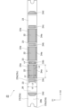
- FIG. 1 is a plan view showing a metal mask according to an embodiment of the present disclosure.
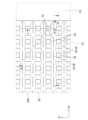
- FIG. 4 is a plan view of the perforated region as viewed from the second surface side. This is a cross-sectional view taken along line I-I' shown in Figure 2A.
- 2B is a cross-sectional view taken along line II-II' shown in FIG. 2A.
- 2B is a cross-sectional view taken along line III-III' shown in FIG. 2A.
- 2B is a perspective view of the region S1 shown in FIG. 2A as viewed from the second surface side.
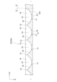
- FIG. 4 is a plan view of the stress dispersion region as viewed from the second surface side.
- FIG. 3B is a perspective view of the region S2 shown in FIG. 3A as viewed from the second surface side.
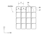
- 10 is a plan view showing an example of an arrangement of recesses in a stress dispersion region.
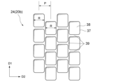
- FIG. 10 is a plan view showing an example of an arrangement of recesses in a stress dispersion region.
- FIG. 10 is a plan view showing an example of an arrangement of recesses in a stress dispersion region.
- FIG. 10 is a plan view showing an example of an arrangement of recesses in a stress dispersion region.
- FIG. 10 is a plan view showing an example of an arrangement of recesses in a stress dispersion region.
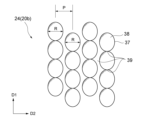
- FIG. 10 is a plan view showing an example of an arrangement of recesses in a stress dispersion region.
- FIG. 10 is a plan view showing an example of an arrangement of recesses in a stress dispersion region.
- FIG. 10 is a plan view showing an example of an arrangement of recesses in a stress dispersion region.
- FIG. 10 is a plan view showing an example of an arrangement of recesses in a stress dispersion region.
- FIG. 1A to 1C are schematic diagrams for explaining an example of a method for manufacturing a metal mask.
- 1A to 1C are diagrams illustrating an example of a process for forming a resist film on a metal plate.
- 1A to 1C are diagrams illustrating an example of a process for patterning a resist film.
- 11A to 11C are diagrams illustrating an example of a first surface etching step in a holed region.
- 11A to 11C are diagrams illustrating an example of a second surface etching step in a holed region.
- FIG. 11A to 11C are diagrams illustrating an example of a second surface etching step in the stress dispersion region.
- FIG. 1 is a diagram showing a metal mask apparatus according to an embodiment of the present disclosure.
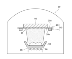
- FIG. 1 is a cross-sectional view illustrating a deposition apparatus according to one embodiment of the present disclosure.
- One or more embodiments may be combined with one or more variations as long as no contradictions arise. One or more embodiments may be combined with each other as long as no contradictions arise. One or more variations may be combined with each other as long as no contradictions arise.
- Numerical ranges expressed with the symbols " ⁇ " and/or “-” include the numerical values placed before and after the symbols “ ⁇ ” and/or “-”. For example, a numerical range expressed as “34-38% by mass” is the same as a numerical range expressed as "34% by mass or more and 38% by mass or less”.
- a numerical range may be defined by combining any one of multiple upper limit candidate values with any one of multiple lower limit candidate values.
- a numerical range may be defined by combining any two of multiple upper limit candidate values, or a numerical range may be defined by combining any two of multiple lower limit candidate values.
- One embodiment of the present disclosure is described in the following paragraphs.
- One embodiment of the present disclosure is an example of an embodiment of the present disclosure.
- the present disclosure is not to be construed as being limited to only one embodiment of the present disclosure.
- the metal mask of the present disclosure can be used for various applications.
- the metal mask of the present disclosure can be used as a metal mask used to pattern an organic material in a desired pattern on a substrate in the manufacture of an organic EL display device.
- the metal mask of the present disclosure can enable patterning with high pixel density.
- Organic EL display devices that can be manufactured include displays for smartphones, televisions, and the like, as well as devices for displaying or projecting images and videos to express virtual reality (VR) and augmented reality (AR).
- VR virtual reality
- AR augmented reality
- a first aspect of the present disclosure is a method for manufacturing a semiconductor device comprising: a perforated region and a peripheral region; the perforated region having a plurality of through holes; the peripheral region is located around the perforated region; the peripheral region includes a stress dispersion region;
- the stress dispersion region has a plurality of recesses,
- the opening shape of the recess in a plan view has a minor axis having a length R,
- the stress dispersion region has the recesses arranged at a pitch P in the minor axis direction,
- the ratio (R/P) of the length R to the pitch P is 0.90 or more. It is a metal mask.
- the recesses are arranged in a staggered or lattice pattern.
- the wall surfaces of adjacent recesses join together.
- a fourth aspect of the present disclosure is a metal mask according to any one of the first to third aspects described above, the thickest portion of the peripheral region has a height H0; The thinnest portion of the stress dispersion region has a height H1, A ratio (H1/H0) of the height H1 to the height H0 is equal to or greater than 0.20 and is equal to or less than 0.90.
- a fifth aspect of the present disclosure is a metal mask according to any one of the first to fourth aspects, the peripheral region has an edge; The stress dispersion region is located between the edge and the perforated region.
- a sixth aspect of the present disclosure is the metal mask of the fifth aspect described above,
- the edge of the peripheral region has a pair of long sides and a pair of short sides,
- the stress dispersion area is located between the edge, which is the long side, and the perforated area.
- a seventh aspect of the present disclosure is the metal mask according to any one of the first to sixth aspects described above, a plurality of said perforated regions; The stress distribution regions are located between a plurality of the perforated regions.
- An eighth aspect of the present disclosure is a metal mask according to any one of the first to seventh aspects,
- the peripheral region has a cut line,
- the cut lines are rows of recesses or through holes,
- the stress dispersion area is located between the cut line and the perforated area.
- a ninth aspect of the present disclosure is a metal mask according to any one of the first to eighth aspects,
- the peripheral region has a cut line,
- the cut lines are rows of recesses or through holes,
- the cut line is located between the stress distribution area and the perforated area.
- a tenth aspect of the present disclosure is a method for manufacturing a semiconductor device comprising: providing a metal plate having a first surface and a second surface opposite the first surface; and an etching step of forming the metal mask by etching the metal plate,
- the metal mask has a hole region and a surrounding region, the perforated region having a plurality of through holes; the peripheral region is located around the perforated region; the peripheral region includes a stress dispersion region;
- the stress dispersion region has a plurality of recesses,
- the opening shape of the recess in a plan view has a minor axis having a length R,
- the stress dispersion region has the recesses arranged at a pitch P in the minor axis direction,
- the ratio (R/P) of the length R to the pitch P is 0.90 or more.
- the metal mask 20 of the present disclosure has a perforated region 22 and a surrounding region 23.
- the perforated region 22 is a region in which a plurality of through holes 25 are formed.
- the surrounding region 23 is a region located around the perforated region 22. Furthermore, the surrounding region 23 has a stress dispersion region 24 with a predetermined recess.
- FIG. 1 shows a plan view of the second surface 20b side of a metal mask 20 according to one embodiment of the present disclosure.
- the metal mask 20 may have a generally rectangular outline in a planar view.
- planar view refers to viewing the metal mask 20 from a surface along the plate surface of the metal mask 20.
- one perforated region 22 may be configured to correspond to one organic EL display device.
- the metal mask 20 may have a plurality of perforated regions 22 arranged in a row at predetermined intervals along the longitudinal direction D2.
- a peripheral region 23 is positioned around each perforated region 22.
- the material that constitutes the metal mask 20 is not particularly limited, but examples include iron alloys containing nickel, iron alloys containing chromium such as stainless steel, nickel, and nickel-cobalt alloys.
- iron alloys containing nickel are preferred.
- the thermal expansion coefficient of the metal mask 20 can be made equivalent to the thermal expansion coefficient of the frame 15 and the thermal expansion coefficient of the substrate 92. This makes it possible to suppress the occurrence of misalignment caused by differences in dimensional changes of the metal mask 20, frame 15, and substrate 92 during the deposition process. Therefore, it is possible to suppress a decrease in the dimensional accuracy and positional accuracy of the deposition material 98 attached to the substrate 92 caused by misalignment.
- iron alloys containing nickel there are no particular limitations on the iron alloys containing nickel, but examples include super Invar materials containing 30% to 34% nickel by mass and also cobalt, Invar materials containing 34% to 38% nickel by mass, and low-thermal expansion Fe-Ni-based plated alloys containing 48% to 54% nickel by mass, and other iron alloys containing 0% to 54% nickel by mass.
- the metal mask 20 of the present disclosure has a first surface 20a and a second surface 20b as the front and back surfaces.
- the first surface 20a and the second surface 20b of the metal mask 20 are distinguished by the diameter of the through holes 25 on the front and back surfaces of the perforated region 22.
- the first surface 20a refers to the surface in the perforated region 22 where the opening area of the through holes 25 is small
- the second surface 20b refers to the surface where the opening area of the through holes 25 is large.
- the area S3 closed by the ridge line 33 surrounding one through hole 25 may be considered to be the opening of the through hole 25.
- the area closed by the ridge line 33 is the opening area.
- the first surface 20a may be the surface of the metal mask 20 facing the substrate 92 when the metal mask device 10 is housed in the deposition device 90 (see FIG. 7).
- the second surface 20b may be the surface of the metal mask 20 located on the side of the crucible 94 holding the deposition material 98 when the metal mask device 10 is housed in the deposition device 90 as shown in FIG. 7 (see FIG. 7).
- FIG. 2A shows a plan view of the perforated region 22 as viewed from the second surface 20b side.
- each perforated region 22 of the metal mask 20 has a plurality of through holes 25.
- the through holes 25 may be formed in a desired pattern.
- the through holes 25 may be arranged in a lattice pattern at a predetermined pitch along two intersecting directions.
- the through holes 25 may also be arranged in a staggered pattern at a predetermined pitch along two intersecting directions.
- the above two directions may correspond to the longitudinal direction D2 or width direction D1 of the metal mask 20.
- the pitch of the through holes 25 in the perforated region 22 is not particularly limited.
- the pitch of the through holes 25 may be approximately 20 ⁇ m or more and 254 ⁇ m or less in both the width direction D1 and the longitudinal direction D2.
- the through holes 25 penetrate from the first surface 20a to the second surface 20b of the metal mask 20 in the thickness direction N.
- the deposition material 98 passes through the through holes 25 and is deposited on the substrate 92. That is, each through hole 25 defines a location on the substrate 92 where the deposition material is deposited.
- the pattern of the through holes 25 in the perforated region 22 corresponds to the pattern in which the deposition material 98 is deposited.
- a metal mask 20 with a different pattern of through holes 25 can be used depending on the type of deposition material 98. Also, if the pattern in which the deposition material 98 is applied is the same regardless of the type, the same metal mask 20 can be used. In this case, different types of deposition materials 98 can be applied in the same pattern by moving the metal mask 20 and the substrate 92 relative to each other.
- the perforated region 22 may include a plurality of through holes 25 and a plurality of ridges 33.
- the ridges 33 may be positioned to separate adjacent through holes 25.
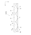
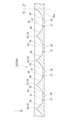
- FIG. 2B is a cross-sectional view taken along line I-I' in FIG. 2A.
- FIG. 2C is a cross-sectional view taken along line II-II' in FIG. 2A.
- the cross-sectional views shown in FIG. 2B and FIG. 2C are cross-sectional views taken when the perforated region 22 is cut in a direction intersecting the through holes 25 and the ridge line 33.
- FIG. 2D is a cross-sectional view taken along line III-III' in FIG. 2A.
- the cross-sectional view in FIG. 2D is a cross-sectional view taken when cutting the perforated region 22 in a direction passing through the through hole 25 and the top portion 32.
- the top portion 32 is the portion of the perforated region 22 where the height is maximum.
- the top portion 32 may also be the portion of the ridge line 33 where the height is maximum.
- the through hole 25 may be formed by connecting a first recess 30 on the first surface 20a side with a second recess 35 on the second surface 20b side.
- the area of the first recess 30 in a plan view may gradually decrease from the first surface 20a to the second surface 20b.
- the area of the second recess 35 in a plan view may gradually decrease from the second surface 20b to the first surface 20a.
- the first recess 30 may be configured as a recess with a smaller diameter than the second recess 35.
- the first wall surface 31 of the first recess 30 and the second wall surface 36 of the second recess 35 may be connected via a circumferential connecting portion 41.
- the connecting portion 41 is a ridge portion that connects the first recess 30 and the second recess 35.
- the direction in which the wall surface of the through hole 25 expands changes discontinuously.
- the opening area of the through hole 25 in a planar view may be minimized at the connecting portion 41.
- the opening area of the through hole 25 in a planar view may be minimized other than at the connecting portion 41.
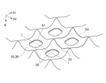
- FIG. 2E shows a perspective view of the region S1 shown in FIG. 2A as viewed from the second surface 20b side.
- ridges 33 separate adjacent through holes 25.
- each through hole 25 may be surrounded by multiple ridges 33.
- the second wall surfaces 36 of adjacent second recesses 35 may merge. This can also be said to be a state in which the second surface 51b of the metal plate 51 constituting the metal mask 20 does not remain between adjacent second recesses 35.
- a ridge line 33 is formed by the merged second wall surfaces 36.
- the height of the ridge line 33 formed by the merged second wall surfaces 36 is not constant, and may vary depending on the distance from the center of the through hole 25. For example, the height of the ridge line 33 may be higher as the distance from the center of the through hole 25 to the ridge line 33 becomes longer.
- Such through holes 25 may be formed by etching the metal plate 51 so that the second surface 51b of the metal plate 51 does not remain between adjacent second recesses 35, as in the manufacturing method described below.
- the second wall surfaces 36 of adjacent second recesses 35 do not have to merge. This can also be said to mean that adjacent second recesses 35 are spaced apart along the surface direction of the second surface 20b. In this case, the portion remaining as the second surface 20b between adjacent second recesses 35 becomes the ridge line 33 that separates adjacent through holes 25. Also, in this case, the ridge line 33 may be the first surface 51a of the metal plate 51 remaining between adjacent first recesses 30. In this case, the height of the ridge line 33 may be constant.
- adjacent through holes 25 may be spaced apart along the surface direction of the first surface 20a.
- the first surface 51a of the metal plate 51 may remain between adjacent first recesses 30.
- the first surface 51a of the metal plate 51 may correspond to the first surface 20a of the metal mask 20, and the second surface 51b of the metal plate 51 may correspond to the second surface 20b of the metal mask 20.
- the surrounding region 23 is a region located around the perforated region 22.
- the surrounding region 23 may be located so as to surround the perforated region 22.
- the surrounding region 23 may be a region that supports the perforated region 22 by being located around the perforated region 22.
- the surrounding area 23 has a predetermined stress distribution area 24. This allows the stress to be distributed more evenly even when tension is applied to the metal mask. This makes the metal mask less likely to wrinkle. In addition, the accuracy of the installation position when placing the metal mask on the frame is improved. Note that there are no particular limitations on the situations in which tension is applied to the metal mask, but examples include when placing the metal mask on the frame and when transporting the metal mask.
- the surrounding region 23 may also be a region through which the deposition material 98 is not intended to pass. From this perspective, the surrounding region 23 may mainly have a non-porous surface in which no through-holes are formed. However, for various purposes, the surrounding region 23 may have a non-porous surface, but may also have localized through-holes in parts other than the non-porous surface that are not intended for the deposition material to pass through. In this disclosure, a "non-porous surface" refers to a surface that does not have through-holes.
- the surrounding area 23 may have an end 23a that is fixed to the frame 15. As shown in FIG. 1, when the metal mask 20 is a long stick, the end 23a may be located at both ends in the longitudinal direction D2. The end 23a may also have a U-shaped notch or the like.
- the end 23a may be configured so that a portion of it can be cut off after the metal mask 20 is fixed to the frame 15. Furthermore, the end 23a may be configured integrally with the other surrounding area 23 as shown in FIG. 1, or may be configured from a member separate from the other surrounding area. In this case, the end may be joined to the other part of the surrounding area by, for example, welding.
- the thickest part of the surrounding region 23 has a height H0.
- the thickest part of the surrounding region 23 may be the height from the first surface 20a to the second surface 20b in the surrounding region 23.
- the height H0 may preferably be 50 ⁇ m or less, 45 ⁇ m or less, 40 ⁇ m or less, 35 ⁇ m or less, 30 ⁇ m or less, 25 ⁇ m or less, or 20 ⁇ m or less.
- the height H0 may preferably be 2.5 ⁇ m or more, 5 ⁇ m or more, 10 ⁇ m or more, or 15 ⁇ m or more. Increasing the height of the surrounding area tends to further improve the strength of the metal mask 20. This tends to further suppress deformation or breakage of the perforated area 22, for example.
- the stress dispersion region 24 has a plurality of recesses 37.
- the recesses 37 in the stress dispersion region 24 are also referred to as "third recesses 37."
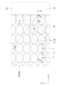
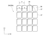
- Figure 3A shows a plan view of the stress dispersion region 24 as seen from the second surface 20b side.
- the stress dispersion region 24 has third recesses 37 arranged at pitch P in the short axis direction.
- the third recesses 37 have a short axis of length R.
- FIG. 3A shows an embodiment in which the short axis direction and the D2 direction are parallel, but this is not limiting.
- the short axis direction may be parallel to the D1 direction, or the short axis direction may not be parallel to the D1 direction or the D2 direction, but may intersect these directions.
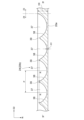
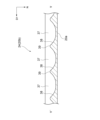
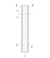
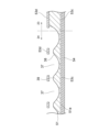
- FIG. 3B is a cross-sectional view taken along line IV-IV' shown in FIG. 3A.
- line IV-IV' may be a line parallel to the short axis direction.
- third wall surfaces 38 of third recesses 37 may join together to form a ridge line 39.
- Ridge line 39 separates adjacent third recesses 37.
- the opening shape of third recesses 37 in plan view may be a shape defined by ridge line 39.
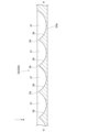
- FIG. 3C is a cross-sectional view taken along line V-V' in FIG. 3A.
- the cross-sectional views shown in FIG. 3B and FIG. 3C are cross-sectional views taken when the stress dispersion region 24 is cut in a direction intersecting the third recess 37 and the ridge 39.
- FIG. 3D is a cross-sectional view taken along line VI-VI' in FIG. 3A.
- the cross-sectional view shown in FIG. 3D is a cross-sectional view taken when the stress dispersion region 24 is cut in a direction passing through the intersection of the third recess 37 and the ridge 39.
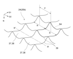
- FIG. 3E shows a perspective view of the region S2 shown in FIG. 3A as viewed from the second surface 20b side.
- ridges 39 separate adjacent third recesses 37.
- each third recess 37 may be surrounded by multiple ridges 39.
- the third recess 37 is formed on the second surface 20b.
- the third recess 37 may be formed on the second surface 20b, the first surface 20a, or both.
- the volume difference between the perforated region 22 and the surrounding region 23 on the second surface 20b side becomes smaller, the stress dispersion effect is improved, and the occurrence of wrinkles during tensioning tends to be suppressed.
- the area of the third recess 37 in a plan view may gradually decrease from the second surface 20b toward the first surface 20a.
- the third recesses 37 may be formed in a desired pattern.
- the third recesses 37 may be arranged in a lattice pattern at a predetermined pitch along two mutually intersecting directions (D1, D2).
- D1, D2 mutually intersecting directions
- adjacent third recesses 37 may be adjacent along the surface direction.
- the third wall surfaces 38 of adjacent third recesses 37 may merge.
- adjacent third recesses 37 may be spaced apart along the surface direction. In other words, the third wall surfaces 38 of adjacent third recesses 37 may not merge.
- adjacent third recesses 37 may be adjacent in a predetermined direction, and adjacent third recesses 37 may be spaced apart in another direction.
- the third recesses 37 may also be arranged in a staggered pattern at a predetermined pitch along two mutually intersecting directions.
- adjacent third recesses 37 may be adjacent along the surface direction.
- the third wall surfaces 38 of adjacent third recesses 37 may merge.
- adjacent third recesses 37 may be spaced apart along the surface direction.
- the third wall surfaces 38 of adjacent third recesses 37 may not merge.
- adjacent third recesses 37 may be adjacent in a predetermined direction, and adjacent third recesses 37 may be spaced apart in another direction.
- the above two directions may correspond to the longitudinal direction D2 or width direction D1 of the metal mask 20.
- the pitch of the third recesses 37 in the stress dispersion region 24 is not particularly limited, but may be approximately 20 ⁇ m or more and 254 ⁇ m or less in both the width direction D1 and the longitudinal direction D2.
- the third recesses 37 may be arranged in any pattern other than the above. In that case, the walls of adjacent third recesses 37 may or may not merge.
- the opening shape of the third recess 37 may have various shapes, such as a circle, an ellipse, or a rectangle.
- the elliptical third recesses 37 may be arranged in a staggered pattern.
- the third recesses 37 may be arranged in a stripe pattern with elongated rectangles.
- the opening shape of the third recess 37 in plan view has a short axis of length R.
- the length R of the short axis may be determined from the opening shape of the third recess 37 on the second surface 20b.
- the length R of the short axis may be determined from the area S4 closed by the ridge line 39 surrounding one third recess 37.
- the minor axis of the opening shape refers to the line segment that passes through the center of gravity of the opening shape and bisects the opening shape and has the shortest length.
- the opening shape is rectangular, the direction of the short axis and the length R match the direction and length of its short side (see Figures 4A to 4E). If the opening shape is square, the direction of the short axis and the length R match the direction and length of one of its sides. If the opening shape is diamond, the direction of the short axis and the length R match the direction and length of the shorter diagonal. If the opening shape is elliptical, the direction of the short axis and the length R match the direction and length of its short diameter (see Figure 4F). If the opening shape is circular, the direction of the short axis and the length R match the direction and length of its diameter.
- pitch P is the distance between the third recesses 37 lined up in the short axis direction.
- Pitch P may also be the distance between the center points of gravity of the third recesses 37 lined up in the short axis direction.
- the third recesses 37 are arranged in a lattice pattern as in Figures 4A to 4B, the distance between adjacent third recesses 37 in the short axis direction is pitch P.
- the third recesses 37 adjacent in the short axis direction are shifted in position in the D1 direction and arranged in a staggered pattern. Even if there is such a shift in position, the distance between adjacent third recesses 37 in the short axis direction is pitch P as in Figures 4C to 4F.
- the minor axis length R may preferably be 250 ⁇ m or less, 225 ⁇ m or less, 200 ⁇ m or less, 175 ⁇ m or less, 150 ⁇ m or less, 125 ⁇ m or less, 100 ⁇ m or less, 75 ⁇ m or less, 50 ⁇ m or less, 40 ⁇ m or less, or 30 ⁇ m or less.
- the minor axis length R may preferably be 10 ⁇ m or more, 20 ⁇ m or more, 30 ⁇ m or more, 40 ⁇ m or more, 50 ⁇ m or more, 60 ⁇ m or more, 70 ⁇ m or more, 80 ⁇ m or more, 90 ⁇ m or more, or 100 ⁇ m or more.
- the stress dispersion region 24 has third recesses 37 arranged at a pitch P in the short axis direction.
- the pitch P may preferably be 300 ⁇ m or less, 250 ⁇ m or less, 225 ⁇ m or less, 200 ⁇ m or less, 175 ⁇ m or less, 150 ⁇ m or less, 125 ⁇ m or less, 100 ⁇ m or less, 75 ⁇ m or less, or 50 ⁇ m or less.
- the pitch P may preferably be 20 ⁇ m or more, 30 ⁇ m or more, 40 ⁇ m or more, 50 ⁇ m or more, 60 ⁇ m or more, 70 ⁇ m or more, 80 ⁇ m or more, 90 ⁇ m or more, or 100 ⁇ m or more.
- the ratio (R/P) of the length R to the pitch P is 0.90 or more, and may be preferably 0.92 or more, 0.94 or more, 0.96 or more, or 0.98 or more.
- the ratio (R/P) may be preferably 1.00 or less, 0.99 or less, or 0.98 or less.
- the pitch P of the third recesses 37 aligned in the minor axis direction is equal to the length R of the minor axis. Therefore, the ratio (R/P) in this case is 1.00.
- the third recesses 37 are configured to be larger and closer together in the stress distribution region 24. This allows the stress to be distributed more evenly by the stress distribution region 24. As a result, even when tension is applied to the metal mask, wrinkles are less likely to occur, improving the installation position accuracy.
- the minor axis length R1 and the ratio (R/P) to be equal to or less than the upper limit, the strength of the metal mask tends to be further improved.
- the pitch P is made equal to or less than the upper limit. This allows stress to be distributed more uniformly by the stress distribution region 24. As a result, even when tension is applied to the metal mask, wrinkles are less likely to occur, improving the installation position accuracy. Furthermore, by making the pitch P equal to or greater than the lower limit, the strength of the metal mask tends to be improved.
- the ranges of the minor axis length R, pitch P, and ratio (R/P) may be determined by a combination of any one of the multiple lower limit candidate values described above and any one of the multiple upper limit candidate values described above.
- the thinnest part of the stress distribution region 24 has a height H1.
- the thinnest part of the stress distribution region 24 may be the bottom part of the third recess 37 in the stress distribution region 24.
- the height H1 may be the height from the first surface 20a to the bottom of the third recess 37.
- the height H1 may be the height from the second surface 20b to the bottom of the third recess 37.
- the bottom of the third recess 37 may be the part in the stress distribution region 24 where the height is minimal.
- the height H1 may preferably be 45 ⁇ m or less, 40 ⁇ m or less, 35 ⁇ m or less, 30 ⁇ m or less, 25 ⁇ m or less, or 20 ⁇ m or less.
- the height H1 may preferably be 2.5 ⁇ m or more, 5 ⁇ m or more, or 10 ⁇ m or more.
- the ratio of height H1 to height H0 may preferably be 0.20 or more, 0.25 or more, 0.30 or more, 0.35 or more, 0.40 or more, or 0.45 or more.
- the ratio of H1 (H1/H0) may preferably be 0.80 or less, 0.75 or less, 0.70 or less, 0.65 or less, 0.60 or less, or 0.55 or less.
- the range of height H1 and ratio (H1/H0) may be determined by combining any one of the multiple lower limit candidate values described above with any one of the multiple upper limit candidate values described above.
- the stress distribution region 24 can be formed at any position in the surrounding region 23. Below, with reference to FIG. 1, examples of the positions of the stress distribution region 24 in the surrounding region 23 are described. FIG. 1 shows stress distribution regions 24a to 24d according to their positions.
- the stress distribution region 24 may be located between the edge 23b of the surrounding region 23 and the perforated region 22.
- the edge 23b of the surrounding region 23 has a pair of long sides 23c and a pair of short sides 23d.
- the stress distribution region 24a may be located between the long sides 23c and the perforated region 22.
- the stress distribution regions 24c, 24d may be located between the short sides 23d and the perforated region 22.
- the stress distribution region 24a may be located around the perforated region 22, or the stress distribution region 24a may be located so as to surround the perforated region 22.
- width L1 of the stress dispersion region 24a and the width L2 of the perforated region 22 may be approximately the same.
- the ratio of width L1 to width L2 (L1/L2) may preferably be 0.80 or more, 0.90 or more, or 1.00 or more.
- the ratio (L1/L2) may preferably be 2.00 or less, 1.50 or less, 1.20 or less, 1.10 or less, or 1.00 or less.
- the width L3 of the stress dispersion regions 24c, 24d and the width L4 of the perforated region 22 may be substantially the same.
- the ratio of width L3 to width L4 (L3/L4) may preferably be 0.80 or more, 0.90 or more, or 1.00 or more.
- the ratio (L3/L4) may preferably be 1.20 or less, 1.10 or less, or 1.00 or less.
- the width L3 of the stress dispersion regions 24c, 24d and the width L0 of the peripheral region 23 may be substantially the same.
- the ratio (L3/L0) of the width L3 to the width L0 may preferably be 0.70 or more, 0.80 or more, or 0.90 or more.
- the ratio (L3/L0) may preferably be 0.95 or less, 0.90 or less, or 0.85 or less.
- the stress dispersion region 24b may be located between the multiple perforated regions 22.
- width L5 of the stress dispersion region 24b and the width L4 of the perforated region 22 may be substantially the same.
- the ratio of width L5 to width L4 (L5/L4) may preferably be 0.80 or more, 0.90 or more, or 1.00 or more.
- the ratio (L5/L4) may preferably be 1.20 or less, 1.10 or less, or 1.00 or less.
- the width L5 of the stress dispersion region 24b and the width L0 of the peripheral region 23 may be substantially the same.
- the ratio of the width L5 to the width L0 (L5/L0) may preferably be 0.70 or more, 0.80 or more, or 0.90 or more.
- the ratio (L5/L0) may preferably be 0.95 or less, 0.90 or less, or 0.85 or less.
- the surrounding region 23 may have a cut line 26.
- the cut line 26 is a cutting line when cutting the surrounding region 23.
- the cut line 26 may be, for example, a row of through holes or half-etched recesses arranged at a predetermined interval.
- the surrounding region 23 may be cut at the cut line 26. For example, after the metal mask 20 is welded to the frame 15, the surrounding region 23 may be cut at the cut line 26 located outside the welded point.
- the stress dispersion region 24c may be located between the cut line 26 and the perforated region 22.
- the stress dispersion region 24d may be located between the cut line 26 and the short side 23d. In other words, the cut line 26 may be located between the stress dispersion region 24d and the perforated region 22.
- the stress dispersion region 24 may be rectangular, or may be approximately fan-shaped, polygonal, circular, or elliptical.
- the perforated region 22 and the stress dispersion region 24 may both have a rectangular shape. In this case, one side of the stress dispersion region 24 may be positioned approximately parallel to one side of the perforated region 22.
- the method for manufacturing a metal mask includes a preparation step of preparing a metal plate 51 having a first surface 51a and a second surface 51b located on the opposite side of the first surface 51a, and an etching step of forming the metal mask 20 by etching the metal plate 51.
- the metal mask 20 may be formed by etching, by laser processing, or by electroforming.
- Figure 5A is a schematic diagram showing a manufacturing apparatus 70 that manufactures the metal mask 20 using a metal plate 51, together with the processing sequence.
- Figure 5A shows an example in which the metal plate 51 is continuously supplied from the resist film forming apparatus 71 to the stripping apparatus 74.
- the manufacturing method of the metal mask 20 of the present disclosure is not limited to this, and for example, the metal plate 51 may be wound into a wound body after each process in each apparatus. Furthermore, when supplying the metal plate 51 to each apparatus, the metal plate 51 may be unwound from the wound body and supplied.
- a metal plate 51 having a desired thickness is prepared (preparation step).
- the metal plate 51 may be in the form of a wound body 50 wound around a core 52.
- the method for producing the metal plate 51 having the desired thickness is not particularly limited, but examples include a rolling method and a plating film formation method.
- resist films 53a, 53b are formed on the first surface 51a and the second surface 51b of the metal plate 51 using a resist film forming device 71 (FIG. 5B).
- the resist films 53a, 53b may be formed by attaching a dry film resist to the first surface 51a and the second surface 51b.
- the resist films 53a, 53b may be formed by applying a coating liquid containing a photosensitive resist material to the first surface 51a and the second surface 51b and drying the coating liquid.
- the resist films 53a and 53b thus formed may be either negative resist or positive resist. Of these, negative resists are preferably used.
- the thickness of the resist films 53a, 53b may be 15 ⁇ m or less, 10 ⁇ m or less, 6 ⁇ m or less, or 4 ⁇ m or less.
- the thickness of the resist films 53a, 53b may be 1 ⁇ m or more, 3 ⁇ m or more, 5 ⁇ m or more, or 7 ⁇ m or more.
- the range of thicknesses of the resist films 53a, 53b may be determined by a combination of any one of the multiple upper limit candidate values described above and any one of the multiple lower limit candidate values described above.
- a first resist pattern 53c is formed on the first surface 51a
- a second resist pattern 53d is formed on the second surface 51b.
- a photomask that does not transmit light to the area of the resist film that is to be removed may be placed on the resist film, the resist film may be exposed through the photomask, and the resist film may be developed.
- the metal plate 51 is etched using the etching device 73 with the first resist pattern 53c and the second resist pattern 53d as masks (etching process).
- the etching process may include a first surface etching process and a second surface etching process.
- FIG. 5D shows a schematic diagram illustrating an example of the first surface etching process in the perforated region 22.
- the region of the first surface 51a that is not covered by the first resist pattern 53c is etched using an etching solution.
- the second surface 51b may be covered with a resin or the like that is resistant to the etching solution.
- the etching solution erodes the first surface 51a that is not covered by the first resist pattern 53c ( Figure 5D). This forms a large number of first recesses 30 on the first surface 51a. Note that etching of the metal plate 51 can proceed isotropically in various directions from the holes in the resist pattern. Therefore, the cross-sectional areas of the first recesses 30 and second recesses 35 at each position along the thickness direction of the metal mask 20 become gradually smaller as they progress from the surface in the thickness direction.
- FIG. 5E shows a schematic diagram illustrating an example of the second surface etching process in the perforated region 22.
- the region of the second surface 51b that is not covered by the second resist pattern 53d is etched using an etching solution.
- a film or the like that covered the second surface 51b in the first surface etching process may be peeled off beforehand.
- the first surface 51a may be covered with a resin 54 or the like that is resistant to the etching solution.
- the etching solution erodes the second surface 51b that is not covered by the second resist pattern 53d (FIG. 5E). This forms a second recess 35 on the second surface 51b. The first recess 30 and the second recess 35 then communicate with each other, thereby forming a through hole 25.
- the etching solution is not particularly limited as long as it is a conventionally known solution, but examples include solutions containing ferric chloride and hydrochloric acid.
- etching may be continued until adjacent second recesses 35 are connected, as shown in FIG. 5E.
- the adjacent second recesses 35 join together to form a ridge line 33.
- the ridge line 33 also moves away from the second resist pattern 53d, and erosion by etching progresses in the thickness direction of the metal plate 51 at the top of the ridge line 33. This causes the second resist pattern 53d to peel off from the metal plate 51.
- the second surface 51b may partially remain between adjacent second recesses 35.
- FIG. 5F shows a schematic diagram illustrating an example of the second surface etching process in the stress dispersion region 24.
- the second recesses 35 in the perforated region 22 and the third recesses 37 in the stress dispersion region 24 may be formed by the same second surface etching process. In the second surface etching process, etching may be continued until adjacent third recesses 37 are connected, as shown in FIG. 5F. At the points where adjacent third recesses 37 are connected, the adjacent third recesses 37 join together to form ridge lines 39.
- the resist pattern and the resin 54 that is resistant to the etching solution are peeled off from the metal plate 51 using a peeling device 74. Then, a separation device 75 is used to cut the long metal plate 51, thereby performing a separation process in which the metal mask 20 made of a sheet-like metal plate is separated from the metal plate 51. In this manner, the metal mask 20 can be obtained.
- the metal mask device 10 has a frame 15 and the above-mentioned metal mask 20 placed on the frame 15.
- the metal mask 20 may be placed on the frame 15 with the second surface 20b in contact with the frame 15.
- Figure 6 shows a plan view of the metal mask device 10 as viewed from the first surface 20a side of the metal mask 20.
- Figure 7 shows a cross-sectional view of the deposition device.
- the metal mask device 10 of the present disclosure may have multiple metal masks 20 attached to one frame (FIG. 6).
- the multiple metal masks 20 may be aligned in a width direction D1 that intersects with the longitudinal direction D2 of the metal masks 20.
- Each metal mask 20 may be fixed to the frame 15 at both ends 23a of the metal mask 20 in the longitudinal direction D2.
- one metal mask 20 as shown in FIG. 1C may be attached to one frame 15.
- the metal mask 20 may be fixed to the frame 15 at the end 23a of the peripheral region 23.
- the method of fixing to the frame 15 is not particularly limited, but examples include welding.
- the metal mask device 10 may include a member that is fixed to the frame 15 and that partially overlaps the metal mask 20 in the thickness direction of the metal mask 20.
- Examples of such members include, but are not limited to, a member that extends in a direction intersecting the longitudinal direction of the metal mask 20 and supports the metal mask 20, a member that overlaps the gap between two adjacent metal masks, etc.
- the organic EL display device may include a substrate 92 and a deposition layer including a deposition material 98 arranged in a pattern, which are stacked together.
- the method for manufacturing an organic EL display device includes, but is not limited to, a deposition process in which a deposition material 98 is deposited on a substrate such as a substrate 92 using a metal mask 20.
- the metal mask device 10 is positioned so that the metal mask 20 faces the substrate 92.
- the first surface 20a of the metal mask 20 may face the substrate 92.
- the substrate 92 is the deposition target, such as a glass substrate.
- the surface of the metal mask 20 facing the substrate 92 is the first surface 20a
- the surface of the metal mask 20 located on the side of the crucible 94 holding the deposition material 98 is the second surface 20b.
- the metal mask 20 is placed on the surface of the substrate 92 facing the crucible 94.
- the metal mask 20 and the substrate 92 may be brought into close contact with each other by magnetic force.
- a crucible 94 containing a deposition material 98 and a heater 96 for heating the crucible 94 may be arranged below the metal mask device 10.
- the deposition material 98 may be, for example, an organic light-emitting material.
- the deposition material 98 in the crucible 94 is vaporized or sublimated by heating from the heater 96.
- the vaporized or sublimated deposition material 98 adheres to the substrate 92 through the through-holes 25 of the metal mask 20.
- the deposition material 98 is formed on the surface of the substrate 92 in a desired pattern corresponding to the positions of the through-holes 25 of the metal mask 20.
- the inside of the deposition device 90 may be a vacuum atmosphere during the deposition process.
- the deposition material 98 may be formed on the surface of the substrate 92 using different metal masks 20 according to the color of the deposition material 98.
- the deposition material 98 for red, the deposition material 98 for green, and the deposition material 98 for blue may be deposited on the substrate 92 in that order.
- the deposition material 98 for red, the deposition material 98 for green, and the deposition material 98 for blue may be deposited in that order by gradually moving the metal mask 20 (metal mask device 10) and the substrate 92 relative to each other along the arrangement direction of the through holes 25 (the aforementioned one direction).
- the method for manufacturing an organic EL display device may include various steps other than the deposition step of depositing a deposition material 98 on a substrate such as the substrate 92 using the metal mask 20.
- the method for manufacturing an organic EL display device may include a step of forming a first electrode on the substrate. A deposition layer is formed on the first electrode.
- the method for manufacturing an organic EL display device may also include a step of forming a second electrode on the deposition layer.
- the method for manufacturing an organic EL display device may also include a sealing step of sealing the first electrode, the deposition layer, and the second electrode provided on the substrate 92.
- the deposition layer formed on a substrate such as substrate 92 using the metal mask 20 is not limited to the light-emitting layer formed by deposition of the organic light-emitting material described above, and may include other layers.
- the deposition layer may include, in order from the first electrode side, a hole injection layer, a hole transport layer, a light-emitting layer, an electron transport layer, an electron injection layer, and the like. In this case, a deposition process using a metal mask 20 corresponding to each layer may be performed.
- the metal mask 20 may have a plurality of rows of the plurality of perforated regions 22.
- the plurality of perforated regions 22 may be arranged in a lattice pattern.
- the stress dispersion region 24 may be located between the edge 23b of the surrounding region 23 and the perforated region 22.
- the stress dispersion region 24 may also be located between the plurality of perforated regions 22.
- one metal mask 20 may be attached to one frame 15.
- the end 23a may be located on the periphery of the metal mask 20.
- the stress dispersion region 24c may be located between the cut line 26 and the perforated region 22.
- the stress dispersion region 24d may be located between the cut line 26 and the short side 23d.
- one perforated region 22 may be configured to accommodate a plurality of organic EL display devices.
- the perforated region 22 may have a first perforated region and a second perforated region.
- one first perforated region may be configured to accommodate one organic EL display device.
- the second perforated region may be positioned so as to divide adjacent first perforated regions.
- the first perforated region and the second perforated region may have different densities of through holes. More specifically, the density of through holes in the first perforated region may be higher than the density of through holes in the second perforated region.
- the density of through holes refers to the total area of through holes per unit area.
- the area of one through hole refers to the area of the opening of the through hole that is smallest in a planar view.
- the opening of the through hole that is smallest in a planar view may be an opening surrounded by the connection portion 41.
- the first recess 30, the second recess 35, and the third recess 37 may be formed by irradiating laser light using a laser irradiator.
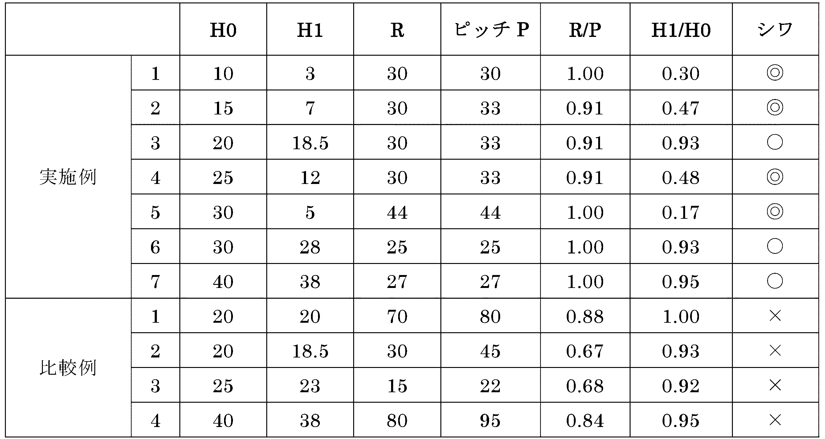
- a metal mask was manufactured having a through hole formed of a first recess and a second recess, and a third recess in a metal plate.
- the minor axis length R of the third recess and the pitch P arranged in the minor axis direction were set to have a predetermined relationship.
- the metal plate used as the raw material for the metal mask was an Invar material.
- Comparative Example A metal mask was obtained in the same manner as in the example, except that the minor axis length R of the third recesses and the pitch P arranged in the minor axis direction had the specified relationship shown in Table 1.
- the waviness that occurs in the width direction of the mask was measured as the amount of waviness after stretch-welding.
- the metal mask stretch-welded to the frame was subjected to three-dimensional measurement using a ⁇ -M1000 manufactured by Shinto S Precision Co., Ltd. to obtain the amount of waviness. Based on the obtained amount of waviness, the occurrence of wrinkles was evaluated according to the following evaluation criteria. . .
- the wave length after tension welding is 100 ⁇ m or less.
- the wave amount after tension welding is more than 100 ⁇ m and 200 ⁇ m or less. ⁇ . . .
- the wave length after the stretching and welding exceeds 200 ⁇ m.
- a wave amount of 100 ⁇ m or less means that the metal mask adheres well to the substrate and there is almost no floating of the metal mask
- a wave amount of more than 100 ⁇ m but less than 200 ⁇ m means that the metal mask adheres to the substrate through magnetization and there is no blurring
- a wave amount of more than 200 ⁇ m means that blurring occurs due to poor adhesion between the metal mask and substrate.
- the "predetermined process” refers to the series of processes that includes manufacturing a metal mask, stretching and welding the manufactured metal mask onto a frame to manufacture a metal mask device, performing deposition using the obtained metal mask device, cleaning the metal mask device, and then using it again for deposition.
- the metal mask of the present invention has industrial applicability, such as for use as a metal mask in the manufacture of organic EL display devices.
- 10...metal mask device 15...frame, 20...metal mask, 20a...first surface, 20b...second surface, 22...perforated area, 23...peripheral area, 23a...end, 23b...edge, 23c...long side, 23d...short side, 24...stress distribution area, 24a...stress distribution area, 24b...stress distribution area, 24c...stress distribution area, 24d...stress distribution area, 25...through hole, 26...cut line, 30...first recess, 31...first wall surface, 32...top portion, 33...ridge line, 35...second recess, 36...second wall surface, 37...first 3 recess, 38... third wall surface, 39... ridge line, 41... connection portion, 50... roll, 51... metal plate, 51a...
Landscapes
- Chemical & Material Sciences (AREA)
- Engineering & Computer Science (AREA)
- Organic Chemistry (AREA)
- Chemical Kinetics & Catalysis (AREA)
- Materials Engineering (AREA)
- Mechanical Engineering (AREA)
- Metallurgy (AREA)
- Manufacturing & Machinery (AREA)
- Optics & Photonics (AREA)
- Physics & Mathematics (AREA)
- Electroluminescent Light Sources (AREA)
- Physical Vapour Deposition (AREA)
- Printing Plates And Materials Therefor (AREA)
- Manufacturing Of Printed Wiring (AREA)
- Manufacture Or Reproduction Of Printing Formes (AREA)
Abstract
Description
有孔領域と、周囲領域と、を有し、
前記有孔領域は、複数の貫通孔を有し、
前記周囲領域は、前記有孔領域の周囲に位置し、
前記周囲領域は、応力分散領域を有し、
前記応力分散領域は、複数の凹部を有し、
前記凹部の平面視における開口形状は、長さRの短軸を有し、
前記応力分散領域は、前記短軸方向にピッチPで並ぶ前記凹部を有し、
前記ピッチPに対する前記長さRの比(R/P)が、0.90以上である。
第1面と、前記第1面の反対側に位置する第2面と、を有する金属板を準備する工程と、
前記金属板をエッチングすることによって前記メタルマスクを形成するエッチング工程と、を備え、
前記メタルマスクは、有孔領域と、周囲領域と、を有し、
前記有孔領域は、複数の貫通孔を有し、
前記周囲領域は、前記有孔領域の周囲に位置し、
前記周囲領域は、応力分散領域を有し、
前記応力分散領域は、複数の凹部を有し、
前記凹部の平面視における開口形状は、長さRの短軸を有し、
前記応力分散領域は、前記短軸方向にピッチPで並ぶ前記凹部を有し、
前記ピッチPに対する前記長さRの比(R/P)が、0.90以上である。
有孔領域と、周囲領域と、を有し、
前記有孔領域は、複数の貫通孔を有し、
前記周囲領域は、前記有孔領域の周囲に位置し、
前記周囲領域は、応力分散領域を有し、
前記応力分散領域は、複数の凹部を有し、
前記凹部の平面視における開口形状は、長さRの短軸を有し、
前記応力分散領域は、前記短軸方向にピッチPで並ぶ前記凹部を有し、
前記ピッチPに対する前記長さRの比(R/P)が、0.90以上である、
メタルマスクである。
前記周囲領域の最も厚い部分は、高さH0を有し、
前記応力分散領域の最も薄い部分は、高さH1を有し、
前記高さH0に対する前記高さH1の比(H1/H0)が、0.20以上0.90以下である。
前記周囲領域は、縁を有し、
前記応力分散領域は、前記縁と前記有孔領域の間に位置する。
前記周囲領域の前記縁は、一対の長辺と一対の短辺とを有し、
前記応力分散領域は、前記長辺である前記縁と前記有孔領域の間に位置する。
複数の前記有孔領域を有し、
前記応力分散領域は、複数の前記有孔領域の間に位置する。
前記周囲領域は、カットラインを有し、
前記カットラインは、凹部又は貫通孔の列であり、
前記応力分散領域は、前記カットラインと前記有孔領域の間に位置する。
前記周囲領域は、カットラインを有し、
前記カットラインは、凹部又は貫通孔の列であり、
前記カットラインは、前記応力分散領域と前記有孔領域の間に位置する。
第1面と、前記第1面の反対側に位置する第2面と、を有する金属板を準備する工程と、
前記金属板をエッチングすることによって前記メタルマスクを形成するエッチング工程と、を備え、
前記メタルマスクは、有孔領域と、周囲領域と、を有し、
前記有孔領域は、複数の貫通孔を有し、
前記周囲領域は、前記有孔領域の周囲に位置し、
前記周囲領域は、応力分散領域を有し、
前記応力分散領域は、複数の凹部を有し、
前記凹部の平面視における開口形状は、長さRの短軸を有し、
前記応力分散領域は、前記短軸方向にピッチPで並ぶ前記凹部を有し、
前記ピッチPに対する前記長さRの比(R/P)が、0.90以上である、
メタルマスクの製造方法である。
第1の変形例として、メタルマスク20は、複数の有孔領域22の列を複数有してもよい。言い換えると、複数の有孔領域22は、格子状に配列されてもよい。この場合にも、応力分散領域24は、周囲領域23の縁23bと有孔領域22との間に位置してもよい。また、応力分散領域24は、複数の有孔領域22の間に位置してもよい。
上述のメタルマスクの製造方法にて、金属板に第1凹部及び第2凹部からなる貫通孔と第3凹部を有するメタルマスクを製造した。この際、第3凹部の短軸長さRと、短軸方向に並ぶピッチPが所定の関係を有するようにした。また、メタルマスクの原材料となる金属板は、インバー材とした。
第3凹部の短軸長さRと、短軸方向に並ぶピッチPが、表1に記載する所定の関係を有するようにしたこと以外は、実施例と同様にして、メタルマスクを得た。
メタルマスク長さ方向に引張力を掛けてメタルマスクをフレームに架張溶接する際に、マスク幅方向に発生する波打ちを、架張溶接後のwave量として測定した。具体的には、メタルマスクをフレームに架張溶接したものを、新東Sプレシジョン(株)製のμ-M1000を用いた3次元測定を行ってWave量を得た。得られたwave量に基づいて、下記評価基準により、シワの発生を評価した。
◎・・・架張溶接後のwave量が100μm以下である。
〇・・・架張溶接後のwave量が100μm超過200μm以下である。
×・・・架張溶接後のwave量が200μm超過である。
Claims (10)
- 有孔領域と、周囲領域と、を有し、
前記有孔領域は、複数の貫通孔を有し、
前記周囲領域は、前記有孔領域の周囲に位置し、
前記周囲領域は、応力分散領域を有し、
前記応力分散領域は、複数の凹部を有し、
前記凹部の平面視における開口形状は、長さRの短軸を有し、
前記応力分散領域は、前記短軸方向にピッチPで並ぶ前記凹部を有し、
前記ピッチPに対する前記長さRの比(R/P)が、0.90以上である、
メタルマスク。 - 前記凹部は、千鳥状又は格子状に配列する、
請求項1に記載のメタルマスク。 - 隣り合う前記凹部の壁面が、合流する、
請求項1に記載のメタルマスク。 - 前記周囲領域の最も厚い部分は、高さH0を有し、
前記応力分散領域の最も薄い部分は、高さH1を有し、
前記高さH0に対する前記高さH1の比(H1/H0)が、0.20以上0.90以下である、
請求項1に記載のメタルマスク。 - 前記周囲領域は、縁を有し、
前記応力分散領域は、前記縁と前記有孔領域の間に位置する、
請求項1に記載のメタルマスク。 - 前記周囲領域の前記縁は、一対の長辺と一対の短辺とを有し、
前記応力分散領域は、前記長辺である前記縁と前記有孔領域の間に位置する、
請求項5に記載のメタルマスク。 - 複数の前記有孔領域を有し、
前記応力分散領域は、複数の前記有孔領域の間に位置する、
請求項1に記載のメタルマスク。 - 前記周囲領域は、カットラインを有し、
前記カットラインは、凹部又は貫通孔の列であり、
前記応力分散領域は、前記カットラインと前記有孔領域の間に位置する、
請求項1に記載のメタルマスク。 - 前記周囲領域は、カットラインを有し、
前記カットラインは、凹部又は貫通孔の列であり、
前記カットラインは、前記応力分散領域と前記有孔領域の間に位置する、
請求項1に記載のメタルマスク。 - メタルマスクの製造方法であって、
第1面と、前記第1面の反対側に位置する第2面と、を有する金属板を準備する工程と、
前記金属板をエッチングすることによって前記メタルマスクを形成するエッチング工程と、を備え、
前記メタルマスクは、有孔領域と、周囲領域と、を有し、
前記有孔領域は、複数の貫通孔を有し、
前記周囲領域は、前記有孔領域の周囲に位置し、
前記周囲領域は、応力分散領域を有し、
前記応力分散領域は、複数の凹部を有し、
前記凹部の平面視における開口形状は、長さRの短軸を有し、
前記応力分散領域は、前記短軸方向にピッチPで並ぶ前記凹部を有し、
前記ピッチPに対する前記長さRの比(R/P)が、0.90以上である、
メタルマスクの製造方法。
Priority Applications (2)
| Application Number | Priority Date | Filing Date | Title |
|---|---|---|---|
| KR1020257008890A KR20250085720A (ko) | 2022-10-07 | 2023-10-02 | 메탈 마스크 및 그 제조 방법 |
| CN202380059382.2A CN119698493A (zh) | 2022-10-07 | 2023-10-02 | 金属掩模及其制造方法 |
Applications Claiming Priority (2)
| Application Number | Priority Date | Filing Date | Title |
|---|---|---|---|
| JP2022162040A JP2024055260A (ja) | 2022-10-07 | 2022-10-07 | メタルマスク及びその製造方法 |
| JP2022-162040 | 2022-10-07 |
Publications (1)
| Publication Number | Publication Date |
|---|---|
| WO2024075703A1 true WO2024075703A1 (ja) | 2024-04-11 |
Family
ID=90608207
Family Applications (1)
| Application Number | Title | Priority Date | Filing Date |
|---|---|---|---|
| PCT/JP2023/035954 Ceased WO2024075703A1 (ja) | 2022-10-07 | 2023-10-02 | メタルマスク及びその製造方法 |
Country Status (5)
| Country | Link |
|---|---|
| JP (1) | JP2024055260A (ja) |
| KR (1) | KR20250085720A (ja) |
| CN (1) | CN119698493A (ja) |
| TW (1) | TW202430669A (ja) |
| WO (1) | WO2024075703A1 (ja) |
Cited By (3)
| Publication number | Priority date | Publication date | Assignee | Title |
|---|---|---|---|---|
| JP7730479B1 (ja) | 2024-05-24 | 2025-08-28 | 大日本印刷株式会社 | マスク、蒸着方法及びデバイスの製造方法 |
| JP2025177938A (ja) * | 2024-05-24 | 2025-12-05 | 大日本印刷株式会社 | マスク及び有機デバイスの製造方法 |
| WO2026053751A1 (ja) * | 2024-09-04 | 2026-03-12 | 大日本印刷株式会社 | メタルマスク及びその製造方法 |
Citations (4)
| Publication number | Priority date | Publication date | Assignee | Title |
|---|---|---|---|---|
| JP2014133934A (ja) * | 2013-01-11 | 2014-07-24 | Dainippon Printing Co Ltd | 蒸着マスクの製造方法および蒸着マスク |
| JP2020109211A (ja) * | 2016-04-01 | 2020-07-16 | エルジー イノテック カンパニー リミテッド | 蒸着用マスク及びこれを用いたoledパネル |
| JP2020531679A (ja) * | 2017-08-25 | 2020-11-05 | 京東方科技集團股▲ふん▼有限公司Boe Technology Group Co.,Ltd. | マスクストリップ及びその製造方法、マスクプレート |
| JP2022512583A (ja) * | 2018-11-19 | 2022-02-07 | エルジー イノテック カンパニー リミテッド | 合金金属板及びこれを含む蒸着用マスク |
-
2022
- 2022-10-07 JP JP2022162040A patent/JP2024055260A/ja active Pending
-
2023
- 2023-10-02 KR KR1020257008890A patent/KR20250085720A/ko active Pending
- 2023-10-02 WO PCT/JP2023/035954 patent/WO2024075703A1/ja not_active Ceased
- 2023-10-02 CN CN202380059382.2A patent/CN119698493A/zh active Pending
- 2023-10-05 TW TW112138216A patent/TW202430669A/zh unknown
Patent Citations (4)
| Publication number | Priority date | Publication date | Assignee | Title |
|---|---|---|---|---|
| JP2014133934A (ja) * | 2013-01-11 | 2014-07-24 | Dainippon Printing Co Ltd | 蒸着マスクの製造方法および蒸着マスク |
| JP2020109211A (ja) * | 2016-04-01 | 2020-07-16 | エルジー イノテック カンパニー リミテッド | 蒸着用マスク及びこれを用いたoledパネル |
| JP2020531679A (ja) * | 2017-08-25 | 2020-11-05 | 京東方科技集團股▲ふん▼有限公司Boe Technology Group Co.,Ltd. | マスクストリップ及びその製造方法、マスクプレート |
| JP2022512583A (ja) * | 2018-11-19 | 2022-02-07 | エルジー イノテック カンパニー リミテッド | 合金金属板及びこれを含む蒸着用マスク |
Cited By (5)
| Publication number | Priority date | Publication date | Assignee | Title |
|---|---|---|---|---|
| JP7730479B1 (ja) | 2024-05-24 | 2025-08-28 | 大日本印刷株式会社 | マスク、蒸着方法及びデバイスの製造方法 |
| JP2025177938A (ja) * | 2024-05-24 | 2025-12-05 | 大日本印刷株式会社 | マスク及び有機デバイスの製造方法 |
| JP2025177923A (ja) * | 2024-05-24 | 2025-12-05 | 大日本印刷株式会社 | マスク、蒸着方法及びデバイスの製造方法 |
| JP7863298B2 (ja) | 2024-05-24 | 2026-05-21 | 大日本印刷株式会社 | マスク及び有機デバイスの製造方法 |
| WO2026053751A1 (ja) * | 2024-09-04 | 2026-03-12 | 大日本印刷株式会社 | メタルマスク及びその製造方法 |
Also Published As
| Publication number | Publication date |
|---|---|
| TW202430669A (zh) | 2024-08-01 |
| CN119698493A (zh) | 2025-03-25 |
| JP2024055260A (ja) | 2024-04-18 |
| KR20250085720A (ko) | 2025-06-12 |
Similar Documents
| Publication | Publication Date | Title |
|---|---|---|
| JP2024055260A (ja) | メタルマスク及びその製造方法 | |
| US11649540B2 (en) | Deposition mask and method of manufacturing deposition mask | |
| JP2022191309A (ja) | 蒸着マスクの製造方法、蒸着マスクが割り付けられた中間製品及び蒸着マスク | |
| US12480200B2 (en) | Method of quality determining of deposition mask, method of manufacturing deposition mask, method of manufacturing deposition mask device, method of selecting deposition mask, and deposition mask | |
| JP2024069290A (ja) | 蒸着マスク及び蒸着マスクの製造方法 | |
| TWI774702B (zh) | 蒸鍍遮罩 | |
| EP3569730B1 (en) | Vapor deposition mask, method for manufacturing vapor deposition mask device, and method for manufacturing vapor deposition mask | |
| KR101761494B1 (ko) | 금속판, 금속판의 제조 방법, 및 금속판을 사용해서 증착 마스크를 제조하는 방법 | |
| CN111500980B (zh) | 蒸镀掩模以及蒸镀掩模的制造方法 | |
| US20230349037A1 (en) | Metal mask and method for manufacturing metal mask | |
| JP2025108354A (ja) | 金属板及びその製造方法、並びに、メタルマスクの製造方法 | |
| TWI887716B (zh) | 金屬遮罩及其製造方法 | |
| WO2026053751A1 (ja) | メタルマスク及びその製造方法 | |
| JP2025036083A (ja) | メタルマスク及びその製造方法 | |
| WO2025220563A1 (ja) | メタルマスク及びその製造方法 | |
| WO2025225401A1 (ja) | メタルマスク及びその製造方法 | |
| JP2023152823A (ja) | メタルマスク及びその製造方法 | |
| JP2023152824A (ja) | メタルマスク及びその製造方法 | |
| US20250222500A1 (en) | Metal plate, method for manufacturing metal plate, and method for manufacturing metal mask | |
| CN223226149U (zh) | 金属掩模 | |
| JP7340160B2 (ja) | 蒸着マスクの製造方法および蒸着マスク |
Legal Events
| Date | Code | Title | Description |
|---|---|---|---|
| 121 | Ep: the epo has been informed by wipo that ep was designated in this application |
Ref document number: 23874830 Country of ref document: EP Kind code of ref document: A1 |
|
| WWE | Wipo information: entry into national phase |
Ref document number: 202380059382.2 Country of ref document: CN |
|
| WWP | Wipo information: published in national office |
Ref document number: 202380059382.2 Country of ref document: CN |
|
| NENP | Non-entry into the national phase |
Ref country code: DE |
|
| WWP | Wipo information: published in national office |
Ref document number: 1020257008890 Country of ref document: KR |
|
| 122 | Ep: pct application non-entry in european phase |
Ref document number: 23874830 Country of ref document: EP Kind code of ref document: A1 |