WO2024075596A1 - Plasma treatment device, power supply system, and frequency control method - Google Patents
Plasma treatment device, power supply system, and frequency control method Download PDFInfo
- Publication number
- WO2024075596A1 WO2024075596A1 PCT/JP2023/034969 JP2023034969W WO2024075596A1 WO 2024075596 A1 WO2024075596 A1 WO 2024075596A1 JP 2023034969 W JP2023034969 W JP 2023034969W WO 2024075596 A1 WO2024075596 A1 WO 2024075596A1
- Authority
- WO
- WIPO (PCT)
- Prior art keywords
- source
- frequency power
- period
- high frequency
- periods
- Prior art date
Links
- 238000000034 method Methods 0.000 title claims description 104
- 238000009832 plasma treatment Methods 0.000 title abstract 2
- 238000012545 processing Methods 0.000 claims description 117
- 239000000758 substrate Substances 0.000 claims description 54
- 230000008859 change Effects 0.000 claims description 33
- 230000004044 response Effects 0.000 claims description 4
- 230000008569 process Effects 0.000 description 55
- 239000007789 gas Substances 0.000 description 43
- 238000010586 diagram Methods 0.000 description 23
- 230000015654 memory Effects 0.000 description 19
- 230000006870 function Effects 0.000 description 12
- 238000004891 communication Methods 0.000 description 6
- 230000002093 peripheral effect Effects 0.000 description 5
- 239000003990 capacitor Substances 0.000 description 4
- 230000004048 modification Effects 0.000 description 4
- 238000012986 modification Methods 0.000 description 4
- 230000000630 rising effect Effects 0.000 description 4
- 238000012546 transfer Methods 0.000 description 4
- 230000005540 biological transmission Effects 0.000 description 3
- 238000004590 computer program Methods 0.000 description 3
- 238000009616 inductively coupled plasma Methods 0.000 description 3
- 150000002500 ions Chemical class 0.000 description 3
- 230000002159 abnormal effect Effects 0.000 description 2
- 238000009792 diffusion process Methods 0.000 description 2
- 239000000835 fiber Substances 0.000 description 2
- 230000003287 optical effect Effects 0.000 description 2
- 238000001020 plasma etching Methods 0.000 description 2
- 230000001902 propagating effect Effects 0.000 description 2
- 230000001105 regulatory effect Effects 0.000 description 2
- 239000004065 semiconductor Substances 0.000 description 2
- 239000007787 solid Substances 0.000 description 2
- 230000003068 static effect Effects 0.000 description 2
- BSYNRYMUTXBXSQ-UHFFFAOYSA-N Aspirin Chemical compound CC(=O)OC1=CC=CC=C1C(O)=O BSYNRYMUTXBXSQ-UHFFFAOYSA-N 0.000 description 1
- PGLIUCLTXOYQMV-UHFFFAOYSA-N Cetirizine hydrochloride Chemical compound Cl.Cl.C1CN(CCOCC(=O)O)CCN1C(C=1C=CC(Cl)=CC=1)C1=CC=CC=C1 PGLIUCLTXOYQMV-UHFFFAOYSA-N 0.000 description 1
- RYGMFSIKBFXOCR-UHFFFAOYSA-N Copper Chemical compound [Cu] RYGMFSIKBFXOCR-UHFFFAOYSA-N 0.000 description 1
- 238000007792 addition Methods 0.000 description 1
- 239000012267 brine Substances 0.000 description 1
- 238000004364 calculation method Methods 0.000 description 1
- 229910052802 copper Inorganic materials 0.000 description 1
- 239000010949 copper Substances 0.000 description 1
- 230000000694 effects Effects 0.000 description 1
- 239000013529 heat transfer fluid Substances 0.000 description 1
- 238000004519 manufacturing process Methods 0.000 description 1
- 238000005259 measurement Methods 0.000 description 1
- 239000013307 optical fiber Substances 0.000 description 1
- HPALAKNZSZLMCH-UHFFFAOYSA-M sodium;chloride;hydrate Chemical compound O.[Na+].[Cl-] HPALAKNZSZLMCH-UHFFFAOYSA-M 0.000 description 1
- 238000006467 substitution reaction Methods 0.000 description 1
- 230000001360 synchronised effect Effects 0.000 description 1
- 210000003813 thumb Anatomy 0.000 description 1
Images


Classifications
-
- H—ELECTRICITY
- H01—ELECTRIC ELEMENTS
- H01L—SEMICONDUCTOR DEVICES NOT COVERED BY CLASS H10
- H01L21/00—Processes or apparatus adapted for the manufacture or treatment of semiconductor or solid state devices or of parts thereof
- H01L21/02—Manufacture or treatment of semiconductor devices or of parts thereof
- H01L21/04—Manufacture or treatment of semiconductor devices or of parts thereof the devices having potential barriers, e.g. a PN junction, depletion layer or carrier concentration layer
- H01L21/18—Manufacture or treatment of semiconductor devices or of parts thereof the devices having potential barriers, e.g. a PN junction, depletion layer or carrier concentration layer the devices having semiconductor bodies comprising elements of Group IV of the Periodic Table or AIIIBV compounds with or without impurities, e.g. doping materials
- H01L21/30—Treatment of semiconductor bodies using processes or apparatus not provided for in groups H01L21/20 - H01L21/26
- H01L21/302—Treatment of semiconductor bodies using processes or apparatus not provided for in groups H01L21/20 - H01L21/26 to change their surface-physical characteristics or shape, e.g. etching, polishing, cutting
- H01L21/306—Chemical or electrical treatment, e.g. electrolytic etching
- H01L21/3065—Plasma etching; Reactive-ion etching
-
- H—ELECTRICITY
- H05—ELECTRIC TECHNIQUES NOT OTHERWISE PROVIDED FOR
- H05H—PLASMA TECHNIQUE; PRODUCTION OF ACCELERATED ELECTRICALLY-CHARGED PARTICLES OR OF NEUTRONS; PRODUCTION OR ACCELERATION OF NEUTRAL MOLECULAR OR ATOMIC BEAMS
- H05H1/00—Generating plasma; Handling plasma
- H05H1/24—Generating plasma
- H05H1/46—Generating plasma using applied electromagnetic fields, e.g. high frequency or microwave energy
Definitions
- Exemplary embodiments of the present disclosure relate to a plasma processing apparatus, a power supply system, and a frequency control method.
- Plasma processing apparatuses are used in plasma processing of substrates.
- the plasma processing apparatus generates plasma from a gas in a chamber by supplying source radio frequency power.
- the plasma processing apparatus uses bias radio frequency power to attract ions from the plasma generated in the chamber to the substrate.
- Patent Document 1 discloses a plasma processing apparatus that modulates the power level and frequency of the bias radio frequency power.
- the present disclosure provides a technique for reducing the degree of reflection of source high frequency power when source high frequency power is supplied alone.
- a plasma processing apparatus in one exemplary embodiment, includes a chamber, a substrate support, a radio frequency power supply, and a controller.
- the substrate support is provided within the chamber.
- the radio frequency power supply is configured to supply source radio frequency power to generate plasma from a gas within the chamber.
- the controller is configured to set the source frequency of the source radio frequency power when the source radio frequency power is supplied alone, depending on the source frequency when the source radio frequency power was previously supplied alone and the degree of reflection of the source radio frequency power, so as to suppress the degree of reflection of the source radio frequency power.
- FIG. 1 is a block diagram of a computer-based system that functions as a controller to control the processing performed in an embodiment of the present disclosure.
- FIG. 1 is a diagram for explaining a configuration example of a plasma processing system.
- FIG. 1 is a diagram for explaining a configuration example of a capacitively coupled plasma processing apparatus.
- 2 is an example timing chart relating to a plasma processing apparatus according to an exemplary embodiment.
- 4 is a flow diagram of a frequency control method according to an exemplary embodiment.
- 11 is an example timing chart related to a plasma processing apparatus according to another exemplary embodiment.
- 13 is an example timing chart relating to a plasma processing apparatus according to yet another exemplary embodiment.
- 13 is an example timing chart relating to a plasma processing apparatus according to yet another exemplary embodiment.
- 13 is an example timing chart relating to a plasma processing apparatus according to yet another exemplary embodiment.
- 13 is an example timing chart relating to a plasma processing apparatus according to yet another exemplary embodiment.
- 13 is an example timing chart relating
- a plasma processing apparatus in one exemplary embodiment, includes a chamber, a substrate support, a radio frequency power supply, and a controller.
- the substrate support is provided within the chamber.
- the radio frequency power supply is configured to supply source radio frequency power to generate plasma from a gas within the chamber.
- the controller is configured to set the source frequency of the source radio frequency power when the source radio frequency power is supplied alone, depending on the source frequency when the source radio frequency power was previously supplied alone and the degree of reflection of the source radio frequency power, so as to suppress the degree of reflection of the source radio frequency power.
- a new apparatus and method uses pulsed high frequency (HF) RF to generate and rapidly stabilize a plasma.
- HF pulsed high frequency
- the high frequency power source under the control of the controller, supplies pulsed power to generate plasma.
- control methods and systems described herein may be implemented using computer programming or engineering techniques, including computer software, firmware, hardware, or any combination or subset thereof.
- the technical effect may include at least processing a substrate in a plasma processing apparatus using a controller to control pulsed radio frequency (HF) RF in generating a plasma.
- HF radio frequency
- FIG. 1 is a block diagram of a computer (as a type of circuit) that can implement various control aspects of embodiments of the present disclosure.
- control aspects of the present disclosure may be implemented as a system, method, and/or computer program product.
- the computer program product may include a computer-readable recording medium having computer-readable program instructions recorded thereon that cause one or more processors to perform aspects of the embodiments.
- a computer-readable storage medium may be a tangible device capable of storing instructions for use by an instruction execution device (processor).
- a computer-readable storage medium may be, for example, but not limited to, an electronic storage device, a magnetic storage device, an optical storage device, an electromagnetic storage device, a semiconductor storage device, or any suitable combination of these devices.
- While not exhaustive, a more specific list of examples of computer-readable storage media includes each of (and suitable combinations of) floppy disks, hard disks, solid-state drives (SSDs), random access memories (RAMs), read-only memories (ROMs), erasable programmable read-only memories (EPROMs or flash), static random access memories (SRAMs), compact disks (CDs or CD-ROMs), digital versatile disks (DVDs), and memory cards or sticks.
- SSDs solid-state drives
- RAMs random access memories
- ROMs read-only memories
- EPROMs or flash erasable programmable read-only memories
- SRAMs static random access memories
- CDs or CD-ROMs compact disks
- DVDs digital versatile disks
- a computer-readable storage medium should not be interpreted as a transitory signal in itself, such as an electric wave or other freely propagating electromagnetic wave, an electromagnetic wave propagating through a waveguide or other transmission medium (e.g., a light pulse through a fiber optic cable), or an electrical signal transmitted through an electrical wire.
- the computer readable program instructions described in this disclosure may be downloaded from a computer readable storage medium to a suitable computer or processing device, or to an external computer or external storage device via a global network (Internet), a local area network, a wide area network, and/or a wireless network.
- the network may include copper transmission lines, optical fiber, wireless transmissions, routers, firewalls, switches, gateway computers, and/or edge servers.
- a network adapter card or network interface of each computer or processing device may receive the computer readable program instructions from the network and transfer the computer readable program instructions to a computer readable storage medium internal to the computer or processing device for storage.
- the computer readable program instructions for performing the operations of the present disclosure may include machine language instructions and/or microcode.
- the machine language instructions and/or microcode may be compiled or translated from source code written in a combination of one or more programming languages, including assembly language, Basic, Fortran, Java, Python, R, C, C++, C#, or similar programming languages. All of the computer readable program instructions may be executed on the user's personal computer, notebook computer, tablet, or smartphone, on a remote computer or computer server, or on a combination of these computing devices.
- the remote computer or computer server may be connected to the user's device or devices through a computer network, such as a local area network, wide area network, or global network (Internet).
- a computer network such as a local area network, wide area network, or global network (Internet).
- an electronic circuit including a programmable logic circuit, a field programmable gate array (FPGA), or a programmable logic array (PLA), may execute the computer readable program instructions to configure or customize the electronic circuit using information from the computer readable program instructions.
- FPGA field programmable gate array
- PLA programmable logic array
- Computer-readable program instructions that may implement the systems and methods described in this disclosure may be provided to one or more processors (and/or one or more cores within a processor) of a general purpose computer, special purpose computer, or other programmable device to produce a machine, whereby the instructions may be executed via the processor of the computer or other programmable device to produce a system that performs the functions shown in the flow diagrams and block diagrams of this disclosure.
- These computer-readable program instructions may be stored on a computer-readable storage medium that can instruct a computer, programmable device, or other device to function in a particular manner, such that the computer-readable storage medium storing the instructions is an article of manufacture that includes instructions that implement aspects of the functionality shown in the flow diagrams and block diagrams of this disclosure.
- Computer-readable program instructions may be loaded into a computer, other programmable apparatus, or other device to cause the computer, other programmable apparatus, or other device to perform a series of operational steps resulting in a computer-implemented process, such that the instructions executed by the computer, other programmable apparatus, or other device may perform the functions illustrated in the flow diagrams and block diagrams of this disclosure.
- FIG. 1 is a functional block diagram illustrating a network system 800 including one or more network computers and servers.
- the hardware and software environment illustrated in FIG. 1 may provide an exemplary platform for implementing the software and/or methods of the present disclosure.
- network system 800 may include, but is not limited to, computer 805, network 810, remote computer 815, web server 820, cloud storage server 825, and computer server 830. In some embodiments, multiple instances of one or more of the functional blocks shown in FIG. 1 may be used.
- FIG. 1 shows further details of computer 805.
- the functional blocks shown in computer 805 are provided only to illustrate example functionality and are not intended to be exhaustive. Details of remote computer 815, web server 820, cloud storage server 825, and computer server 830 are not shown, although these other computers and devices may include functionality similar to that shown for computer 805.
- Computer 805 may be a personal computer (PC), a desktop computer, a notebook computer, a tablet computer, a netbook computer, a personal digital assistant (PDA), a smartphone, or any other programmable electronic device capable of communicating with other devices over network 810.
- PC personal computer
- PDA personal digital assistant
- Computer 805 may include a processor 835, a bus 837, memory 840, non-volatile storage 845, a network interface 850, a peripherals interface 855, and a display interface 865.
- processor 835 may be implemented as a separate electronic subsystem (an integrated circuit chip or a combination of chips and related devices) in some embodiments, while in other embodiments a combination of functions may be implemented on a single chip (sometimes referred to as a system on chip (SoC)).
- SoC system on chip
- Processor 835 may be one or more single-chip or multi-chip microprocessors designed and/or manufactured by Intel Corporation, Advanced Micro Devices, Inc. (AMD), Arm Holdings, Apple Computer, etc.
- microprocessors include Intel Corporation's Celeron, Pentium, Core i3, Core i5, and Core i7, AMD's Opteron, Phenom, Athlon, Turion, and Ryzen, and Arm's Cortex-A, Cortex-R, and Cortex-M.
- Bus 837 may be a proprietary or industry standard high speed parallel interconnect bus or serial interconnect bus such as ISA, PCI, PCI Express (PCI-e), or AGP.
- Memory 840 and non-volatile storage 845 may be computer readable storage media.
- Memory 840 may include suitable volatile storage devices such as dynamic random access memory (DRAM), static random access memory (SRAM), etc.
- Non-volatile storage 845 may include one or more of a floppy disk, a hard disk, a solid state drive (SSD), a read only memory (ROM), an erasable programmable read only memory (EPROM or Flash), a compact disk (CD or CD-ROM), a digital versatile disk (DVD), and a memory card or memory stick.
- DRAM dynamic random access memory
- SRAM static random access memory
- Non-volatile storage 845 may include one or more of a floppy disk, a hard disk, a solid state drive (SSD), a read only memory (ROM), an erasable programmable read only memory (EPROM or Flash), a compact disk (CD or CD-ROM), a digital versatile disk (DVD), and a memory card or memory stick.
- SSD solid state
- Programs 848 may be a collection of machine-readable instructions and/or data that are stored in non-volatile storage 845 and used to create, manage, and control the software functions described and illustrated in more detail elsewhere in this disclosure.
- memory 840 may be significantly faster than non-volatile storage 845.
- programs 848 may be transferred from non-volatile storage 845 to memory 840 prior to execution by processor 835.
- Network 810 may be, for example, a local area network (LAN), a wide area network (WAN) such as the Internet, or a combination of the two, and may include wired, wireless, or fiber optic connections.
- network 810 may be any combination of connections or protocols that support communication between two or more computers and related devices.
- the peripheral interface 855 may allow data input and output to and from other devices that are locally connected to the computer 805.
- the peripheral interface 855 may provide a connection to, for example, an external device 860.
- the external device 860 may include devices such as a keyboard, a mouse, a keypad, a touch screen, and/or other suitable input devices.
- the external device 860 may also include portable computer-readable storage media such as thumb drives, portable optical disks, portable magnetic disks, and memory cards.
- Software and data used to perform embodiments of the present disclosure, such as the program 848, may be stored on a portable computer-readable storage medium. In such an embodiment, the software may be loaded into the non-volatile storage 845 or may be loaded directly into the memory 840 via the peripheral interface 855.
- the peripheral interface 855 may be connected to the external device 860 using industry standard connections such as RS-232 or Universal Serial Bus (USB).
- Display interface 865 may connect computer 805 to a display 870.
- display 870 may be used to present a command line or graphical user interface to a user of computer 805.
- Display interface 865 may connect to display 870 using one or more proprietary or industry standard connections, such as VGA, DVI, DisplayPort, and HDMI.
- the network interface 850 provides communication with other computer systems/devices and storage systems/devices external to the computer 805.
- the software programs and data described herein may be downloaded to the non-volatile storage 845 via the network interface 850 and the network 810 from a remote computer 815, a web server 820, a cloud storage server 825, a computer server 830, etc.
- the systems and methods described herein may be performed by one or more computers connected to the computer 805 via the network interface 850 and the network 810.
- the systems and methods of the present disclosure may be performed by a remote computer 815, a computer server 830, or a combination of interconnected computers on the network 810.
- the data, data sets, and/or databases used in the embodiments of the systems and methods described herein may be stored on or downloaded from the remote computer 815, web server 820, cloud storage server 825, and computer server 830.
- a circuit can be defined as one or more of an electronic component (such as a semiconductor device), multiple components connected directly to each other or connected by electronic communication, a computer, a network of computer devices, a remote computer, a web server, a cloud storage server, and a computer server.
- an electronic component such as a semiconductor device
- a computer, a remote computer, a web server, a cloud storage server, and a computer server can each be included in the circuit or can include a circuit as a component thereof.
- multiple instances of one or more of these components may be used, in which case each of the multiple instances of one or more of these components may be included in the circuit or can include a circuit.
- the circuit represented by a network system may include a serverless computer system corresponding to a virtual set of multiple hardware resources.
- the circuit represented by a computer may include a personal computer (PC), a desktop computer, a notebook computer, a tablet computer, a netbook computer, a personal digital assistant (PDA), a smartphone, and other programmable devices capable of communicating with other devices over a network.
- the circuit may be a general purpose computer, a special purpose computer, or other programmable device described herein having one or more processors.
- Each processor may be one or more single-chip or multi-chip microprocessors.
- a processor is considered to be a processing circuit or circuitry because it has transistors and other circuitry.
- a circuitry may implement the systems and methods of the present disclosure based on computer readable program instructions provided to one or more processors (and/or one or more cores within a processor) of one or more general purpose computers, special purpose computers, or other programmable devices described herein to cause the machine to implement the systems and methods of the present disclosure, such that the instructions are included in the circuitry or executed by one or more processors of a programmable device including the circuitry to cause a system to implement the functions identified in the flow diagrams and block diagrams of the present disclosure.
- a circuitry may be a pre-programmed configuration such as a programmable logic device, dedicated integrated circuit, or the like, and is considered to be a circuitry whether used alone or in combination with other programmable or pre-programmed circuits.
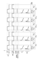
- FIG. 2 is a diagram for explaining an example of the configuration of a plasma processing system.
- the plasma processing system includes a plasma processing device 1 and a control unit 2.
- the plasma processing device 1 includes a plasma processing chamber 10, a substrate support unit 11, and a plasma generation unit 12.
- the plasma processing chamber 10 has a plasma processing space.
- the plasma processing chamber 10 also has at least one gas supply port for supplying at least one processing gas to the plasma processing space, and at least one gas exhaust port for exhausting gas from the plasma processing space.
- the gas supply port is connected to a gas supply unit 20 described later, and the gas exhaust port is connected to an exhaust system 40 described later.
- the substrate support unit 11 is disposed in the plasma processing space, and has a substrate support surface for supporting a substrate.
- the plasma generating unit 12 is configured to generate plasma from at least one processing gas supplied into the plasma processing space.
- the plasma formed in the plasma processing space may be capacitively coupled plasma (CCP), inductively coupled plasma (ICP), electron-cyclotron-resonance plasma (ECR plasma), helicon wave plasma (HWP), or surface wave plasma (SWP).
- CCP capacitively coupled plasma
- ICP inductively coupled plasma
- ECR plasma electron-cyclotron-resonance plasma
- HWP helicon wave plasma
- SWP surface wave plasma
- various types of plasma generating units may be used, including an alternating current (AC) plasma generating unit and a direct current (DC) plasma generating unit.
- the control unit 2 processes computer-executable instructions that cause the plasma processing apparatus 1 to perform the various steps described in this disclosure.
- the control unit 2 may be configured to control each element of the plasma processing apparatus 1 to perform the various steps described herein. In one embodiment, a part or all of the control unit 2 may be included in the plasma processing apparatus 1.
- the control unit 2 may include, for example, a computer 2a.
- the computer 2a may include, for example, a processing unit (CPU: Central Processing Unit) 2a1, a memory unit 2a2, and a communication interface 2a3.
- the processing unit 2a1 may be configured to perform various control operations based on a program stored in the memory unit 2a2.
- the memory unit 2a2 may include a RAM (Random Access Memory), a ROM (Read Only Memory), a HDD (Hard Disk Drive), a SSD (Solid State Drive), or a combination thereof.
- the communication interface 2a3 may communicate with the plasma processing device 1 via a communication line such as a LAN (Local Area Network).
- FIG. 3 is a diagram for explaining a configuration example of a capacitively coupled plasma processing device.
- the capacitively coupled plasma processing apparatus 1 includes a plasma processing chamber 10, a gas supply unit 20, a power supply system 30, and an exhaust system 40.
- the plasma processing apparatus 1 also includes a substrate support 11 and a gas inlet.
- the gas inlet is configured to introduce at least one processing gas into the plasma processing chamber 10.
- the gas inlet includes a shower head 13.
- the substrate support 11 is disposed in the plasma processing chamber 10.
- the shower head 13 is disposed above the substrate support 11. In one embodiment, the shower head 13 constitutes at least a part of the ceiling of the plasma processing chamber 10.
- the plasma processing chamber 10 has a plasma processing space 10s defined by the shower head 13, a sidewall 10a of the plasma processing chamber 10, and the substrate support 11.
- the sidewall 10a is grounded.
- the shower head 13 and the substrate support 11 are electrically insulated from the housing of the plasma processing chamber 10.
- the substrate support 11 includes a main body 111 and a ring assembly 112.
- the main body 111 has a central region (substrate support surface) 111a for supporting a substrate (wafer) W, and an annular region (ring support surface) 111b for supporting the ring assembly 112.
- the annular region 111b of the main body 111 surrounds the central region 111a of the main body 111 in a planar view.
- the substrate W is disposed on the central region 111a of the main body 111
- the ring assembly 112 is disposed on the annular region 111b of the main body 111 so as to surround the substrate W on the central region 111a of the main body 111.
- the main body 111 includes a base 111e and an electrostatic chuck 111c.
- the base 111e includes a conductive member.
- the conductive member of the base 111e functions as a lower electrode.
- the electrostatic chuck 111c is disposed on the base 111e.
- the upper surface of the electrostatic chuck 111c has a substrate support surface 111a.
- the ring assembly 112 includes one or more annular members. At least one of the one or more annular members is an edge ring.
- the substrate support 11 may include a temperature adjustment module configured to adjust at least one of the electrostatic chuck 111c, the ring assembly 112, and the substrate W to a target temperature.
- the temperature adjustment module may include a heater, a heat transfer medium, a flow path, or a combination thereof.
- a heat transfer fluid such as brine or gas flows through the flow path.
- the substrate support 11 may also include a heat transfer gas supply unit configured to supply a heat transfer gas between the back surface of the substrate W and the substrate support surface 111a.
- the shower head 13 is configured to introduce at least one processing gas from the gas supply unit 20 into the plasma processing space 10s.
- the shower head 13 has at least one gas supply port 13a, at least one gas diffusion chamber 13b, and multiple gas inlets 13c.
- the processing gas supplied to the gas supply port 13a passes through the gas diffusion chamber 13b and is introduced into the plasma processing space 10s from the multiple gas inlets 13c.
- the shower head 13 also includes a conductive member.
- the conductive member of the shower head 13 functions as an upper electrode.
- the gas introduction unit may include one or more side gas injectors (SGI) attached to one or more openings formed in the side wall 10a.
- SGI side gas injectors
- the gas supply unit 20 may include one or more gas sources 21 and at least one or more flow controllers 22.
- the gas supply unit 20 is configured to supply one or more process gases from respective gas sources 21 through respective flow controllers 22 to the showerhead 13.
- Each flow controller 22 may include, for example, a mass flow controller or a pressure-controlled flow controller.
- the gas supply unit 20 may include one or more flow modulation devices to modulate or pulse the flow rate of one or more process gases.
- the exhaust system 40 may be connected to, for example, a gas exhaust port 10e provided at the bottom of the plasma processing chamber 10.
- the exhaust system 40 may include a pressure regulating valve and a vacuum pump. The pressure in the plasma processing space 10s is adjusted by the pressure regulating valve.
- the vacuum pump may include a turbomolecular pump, a dry pump, or a combination thereof.
- the plasma processing apparatus 1 further includes a power supply system 30.
- the power supply system 30 includes a high-frequency power supply 31 and a control unit 30c.
- the power supply system 30 may further include a bias power supply 32.
- the power supply system 30 may further include one or more sensors 31s.
- the high frequency power supply 31 is configured to generate a source high frequency power HF to generate a plasma in the chamber (plasma processing chamber 10).
- the source high frequency power HF has a source frequency fS .
- the source frequency fS is, for example, a frequency in the range of 13 MHz or more and 200 MHz or less.
- the source frequency fS may be set to 27 MHz, 40.68 MHz, 60 MHz, or 100 MHz.
- the power level of the source high frequency power HF is, for example, 500 W or more and 20 kW or less.
- the high frequency power supply 31 may include a high frequency signal generator 31g and an amplifier 31a.
- the high frequency signal generator 31g generates a high frequency signal.
- the amplifier 31a generates a source high frequency power HF by amplifying the high frequency signal input from the high frequency signal generator 31g, and outputs the source high frequency power HF.
- the high frequency signal generator 31g may be composed of a programmable processor or a programmable logic device such as an FPGA.
- a D/A converter may be connected between the high frequency signal generator 31g and the amplifier 31a.
- the high frequency power supply 31 is connected to the high frequency electrode via a matching device 31m.
- the base 111e constitutes the high frequency electrode.
- the high frequency electrode may be an electrode provided in the electrostatic chuck 111c.
- the high frequency electrode may be a common electrode with a bias electrode described later.
- the high frequency electrode may be an upper electrode.
- the matching device 31m includes a matching circuit.
- the matching circuit of the matching device 31m has a variable impedance.
- the matching circuit of the matching device 31m is controlled by the control unit 30c.
- the impedance of the matching circuit of the matching device 31m is adjusted so as to match the impedance of the load side of the high frequency power supply 31 to the output impedance of the high frequency power supply 31.
- One or more sensors 31s may be connected between the high frequency power supply 31 and the matching device 31m.
- One or more sensors 31s may be connected between the matching device 31m and the high frequency electrode.
- one or more sensors 31s may be connected between the bias electrode and a junction of an electrical path extending from the matching device 31m toward the bias electrode and an electrical path extending from the matching device 32m described below toward the bias electrode.
- one or more sensors 31s may be connected between the junction and the matching device 31m. Note that one or more sensors 31s may be a sensor separate from the matching device 31m, or may be part of the matching device 31m.
- the one or more sensors 31s may include a directional coupler.
- the directional coupler is configured to detect the power level of the reflected wave of the source high frequency power HF returned from the load of the high frequency power source 31 and to notify the control unit 30c of the detected power level of the reflected wave.
- the one or more sensors 31s may also include a VI sensor configured to detect a voltage VHF and a current IHF of the source high frequency power and to determine an impedance ZL on the load side of the high frequency power supply 31 from the voltage VHF and the current IHF .
- the VI sensor may be configured to determine a phase difference between the voltage VHF and the current IHF .
- the bias power supply 32 is electrically connected to the bias electrode.
- the base 111e constitutes the bias electrode.
- the bias electrode may be an electrode provided in the electrostatic chuck 111c.
- the bias power supply 32 is configured to provide an electric bias EB (or bias energy) to the bias electrode.
- the bias power supply 32 may be configured to provide a pulse of the electric bias EB to the bias electrode.
- the bias power supply 32 may specify the timing of each of the multiple pulses by a signal provided from the pulse controller 34.
- the control unit 2 may function as the pulse controller 34.
- the electric bias EB has a waveform period. That is, the electric bias EB is applied periodically to the bias electrode at a time interval of the waveform period.
- the waveform period of the electric bias EB is the shortest period of the waveform of the electric bias EB and has a time length that is the reciprocal of the bias frequency of the electric bias EB.
- the bias frequency may be smaller than the source frequency.
- the bias frequency may be 100 kHz or more and 28 MHz or less, for example, 400 kHz or 3.2 MHz.
- the electrical bias EB may be a bias high frequency power having a bias frequency.
- the bias power supply 32 is connected to the bias electrode via a matching device 32m.
- the matching device 32m includes a matching circuit.
- the matching circuit of the matching device 32m has a variable impedance.
- the matching circuit of the matching device 32m is controlled by the control unit 30c.
- the impedance of the matching circuit of the matching device 32m is adjusted so as to match the impedance of the load side of the bias power supply 32 to the output impedance of the bias power supply 32.
- the power level of the bias high frequency power may be 500 W or more and 50 kW or less.
- the electric bias EB may include a voltage pulse that is periodically applied to the bias electrode at a time interval of a waveform period.
- the voltage pulse may be a negative voltage pulse or a negative DC voltage pulse (a pulse generated by generating a negative DC voltage waveform), or may be another voltage pulse.
- the voltage pulse may have a waveform such as a triangular wave or a square wave.
- the voltage pulse may have any other pulse waveform.
- the bias power supply 32 may include a signal generator 32g and an amplifier 32a.
- the signal generator 32g generates a signal for generating an electric bias EB from the signal generator 32g.
- the amplifier 32a generates the electric bias EB by amplifying the signal input from the signal generator 32g, and supplies the generated electric bias EB to the bias electrode.
- the signal generator 32g may be composed of a programmable processor or a programmable logic device such as an FPGA.
- a D/A converter may be connected between the signal generator 32g and the amplifier 32a.
- the bias power supply 32 is synchronized with the high frequency power supply 31.
- a synchronization signal used for this purpose may be provided from the bias power supply 32 to the high frequency power supply 31.
- the synchronization signal may be provided from the high frequency power supply 31 to the bias power supply 32.
- the synchronization signal may be provided to the high frequency power supply 31 and the bias power supply 32 from another device such as the control unit 30c.
- the control unit 30c is configured to control the high frequency power supply 31.
- the control unit 30c may be configured with a processor such as a CPU.
- the control unit 30c may be part of the matching device 31m, may be part of the high frequency power supply 31, or may be a control unit separated from the matching device 31m and the high frequency power supply 31.
- the control unit 2 may also function as the control unit 30c.
- the control unit 30c sets the source frequency fs during a period PHO (sole supply period) in which the source radio frequency power HF is supplied alone to generate plasma in the chamber 10, so as to suppress the degree of reflection of the source radio frequency power HF.
- the control unit 30c sets the source frequency fs at each time point during the period PHO , so as to suppress the degree of reflection of the source radio frequency power HF, depending on the source frequency fS and the degree of reflection of the source radio frequency power HF when the source radio frequency power HF was previously supplied alone.
- the period PHO is a period in which the electric bias EB is not supplied and the source radio frequency power HF is supplied alone.
- the degree of reflection may be obtained as the power level of the reflected wave of the source high frequency power HF.
- the degree of reflection may be obtained as a value of the ratio of the power level of the reflected wave of the source high frequency power HF to the power level of the forward wave of the source high frequency power HF or the set output power level of the source high frequency power HF.
- the degree of reflection may be obtained as the amount of deviation of the impedance ZL from the characteristic impedance (e.g., 50 ⁇ ) of the power line of the source high frequency power HF to the high frequency electrode.
- the degree of reflection may be obtained as the phase difference between the voltage VHF and the current IHF .
- the degree of reflection may be obtained as another quantity representing the degree of matching to the plasma at the source frequency fS .
- the degree of reflection may be obtained by one or more sensors 31s or may be determined from measurements obtained by one or more sensors 31s.
- FIG. 4 is a timing chart of an example related to a plasma processing apparatus according to an exemplary embodiment.
- FIG. 4 shows a timing chart of the source high frequency power HF, the frequency setting method, and the source frequency fS in the first embodiment.
- “ON" of the source high frequency power HF indicates that the source high frequency power HF is being supplied
- "OFF" of the source high frequency power HF indicates that the supply of the source high frequency power HF is stopped.
- the frequency setting method shows a setting method of the source frequency fS .
- the frequency setting method includes a sequential feedback process FSB.
- the frequency setting method may further include a start-up process FSA.
- a source high frequency power HF is supplied to generate plasma, but an electric bias EB is not used.
- the plasma processing apparatus 1 does not need to include a bias power supply 32 and a matching device 32m.
- the plasma processing apparatus 1 does not need to include a pulse controller 34.
- the high frequency power supply 31 starts supplying the source high frequency power HF at the start of the period PHO as shown in Fig. 4.
- the high frequency power supply 31 continuously supplies the source high frequency power HF during the period PHO . That is, in the first embodiment, the high frequency power supply 31 supplies a continuous wave of the source high frequency power HF during the period PHO .
- the period P HO includes a number of sub-periods SP, i.e., I sub-periods SP 1 , SP 2 , ..., SPI .
- the sub-periods SP 1 , SP 2 , ..., SPI divide the period P B in the period P HO into I sub-periods.
- the time lengths of the sub-periods SP may be the same as each other or may be different from each other.
- the time length of each of the sub-periods SP may be 10 nsec or more and 10 ⁇ sec or less.
- the period P HO may further include a ramp-up period P S before the plurality of sub-periods SP.
- the ramp-up period P S may include a period for igniting plasma.
- the high frequency power supply 31 may start supplying the source high frequency power HF at the start of the ramp-up period P S.
- the period P B may be a period following the ramp-up period P S.
- the control unit 30c performs the start-up process FSA during the start-up period Ps . Specifically, the control unit 30c changes the source frequency fs according to the initial frequency set during the period from the start to the end of the start-up period Ps .
- the initial frequency set is prepared in advance and stored in a storage unit accessible by the control unit 30c. The initial frequency set may be experimentally obtained or may be determined based on past processing results.
- the control unit 30c performs a sequential feedback process FSB in a period P B following the start-up period P S. Specifically, the control unit 30c sets the source frequency f S [i] in the i-th subperiod SP i so as to suppress the degree of reflection of the source high frequency power HF in the subperiod SP i in accordance with the source frequency f S and the degree of reflection of the source high frequency power HF in each of one or more subperiods prior to the i-th subperiod SP i among the multiple subperiods.
- one or more subperiods before the subperiod SP i may include a subperiod SP iv (first subperiod) and a subperiod SP i-u (second subperiod), where v and u are integers equal to or greater than 1, and v is greater than u. v may be 2, and u may be 1. Note that, when the time length of each of the multiple subperiods SP is short, u may be equal to or greater than 20 in order to reduce the calculation load. For example, when the time length of each of the multiple subperiods SP is 50 nsec, the subperiod SP i is a period 1 ⁇ sec after the subperiod SP i-u .
- the control unit 30c may set the source frequency f S [i] so as to suppress the degree of reflection of the source high frequency power HF in the subperiod SP i in accordance with the change from the source frequency f S [i-v] in the subperiod SP iv to the source frequency f S [i-u] in the subperiod SP i-u and the change from the degree of reflection of the source high frequency power HF in the subperiod SP iv to the degree of reflection of the source high frequency power HF in the subperiod SP i-u.
- the control unit 30c sets the frequency obtained by applying a change in the source frequency f s [i-u] in the same direction as the change from the source frequency f s [i-v] to the source frequency f s [i-u] as the source frequency f s [i].
- the control unit 30c sets the frequency obtained by applying a change in the source frequency f s [i-u] in the opposite direction to the change from the source frequency f s [i-v] to the source frequency f s [ i-u] as the source frequency f s [i].
- the degree of reflection of the source high frequency power HF is reduced during a period in which the source high frequency power HF is supplied solely and continuously.
- the rise time until the plasma is stabilized can be accelerated.
- abnormal discharge of the plasma can be suppressed.
- the operation of the variable capacitance capacitor of the matching device 31m is reduced, and the life of the variable capacitance capacitor can be improved.
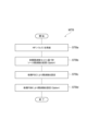
- method MTA is a flow diagram of a frequency control method according to one exemplary embodiment.
- the frequency control method shown in FIG. 5 (hereinafter referred to as "method MTA") may be performed in a chamber 10 with a substrate W placed on a substrate support 11.
- plasma processing may be performed on the substrate W.
- the plasma processing in method MTA may include plasma etching of the substrate W.
- step STAa source radio frequency power HF is supplied from the radio frequency power supply 31 to generate plasma from the gas in the chamber 10.
- the source radio frequency power HF is supplied continuously. That is, a continuous wave of source radio frequency power HF is supplied.
- the method MTA may further include a step STAb.
- the step STAb is performed in the start-up period PS .
- the start-up process FSA described above in relation to the first embodiment is performed.
- the sequential feedback process FSB described above in relation to the first embodiment is performed. That is, in the process STAc, the source frequency fS when the source high frequency power HF is supplied alone is set so as to suppress the degree of reflection of the source high frequency power HF according to the source frequency fS when the source high frequency power HF was previously supplied alone and the degree of reflection of the source high frequency power HF.
- FIG. 6 is a timing chart of an example related to a plasma processing apparatus according to another exemplary embodiment.
- FIG. 6 shows a timing chart of the source high frequency power HF, the electric bias EB, the frequency setting method, the source frequency f S , and the reflection degree RD in the second embodiment.
- the "HIGH" of the source high frequency power HF indicates that the power level of the source high frequency power HF is higher than the power level of the source high frequency power HF indicated by "LOW”.
- the "OFF" of the source high frequency power HF indicates that the supply of the source high frequency power HF is stopped.
- FIG. 6 shows a timing chart of an example related to a plasma processing apparatus according to another exemplary embodiment.
- FIG. 6 shows a timing chart of the source high frequency power HF, the electric bias EB, the frequency setting method, the source frequency f S , and the reflection degree RD in the second embodiment.
- the "HIGH" of the source high frequency power HF indicates that the power level of the source high frequency power HF
- the frequency setting method indicates the setting method of the source frequency f S.
- the frequency setting method includes a start-up process FSA, a sequential feedback process FSB, and an inter-pulse feedback process FSC.
- the high frequency power supply 31 is configured to supply a source high frequency power HF in one of two periods in each of a plurality of pulse periods PC (i.e., pulse periods PC1 , PC2 , ).
- the plurality of pulse periods PC appear in sequence.
- Each of the plurality of pulse periods PC includes periods PBO and PHO .
- the period PHO is one of the two periods in each of the plurality of pulse periods PC, and the period PBO is the other period.
- the high frequency power supply 31 supplies source high frequency power HF whose power level is indicated as "LOW” in a period P HO in each of the multiple pulse periods PC. Also, the high frequency power supply 31 supplies source high frequency power HF whose power level is indicated as "HIGH” in a period P BO in each of the multiple pulse periods PC. That is, the power level of the source high frequency power HF in the period P HO in each of the multiple pulse periods PC is lower than the power level of the source high frequency power HF in the period P BO in each of the multiple pulse periods PC. Note that the power level of the source high frequency power HF in the period P HO in each of the multiple pulse periods PC may be higher than the power level of the source high frequency power HF in the period P BO in each of the multiple pulse periods PC.
- the bias power supply 32 stops supplying the electric bias EB to the substrate support 11 during the period P HO . Also, the bias power supply 32 supplies the electric bias EB to the substrate support 11 during the period P BO . That is, the period P HO is an independent supply period during which the source high frequency power HF is supplied alone without supplying the electric bias EB.
- the period P HO i.e., the single supply period, includes a ramp-up period P S including its start point.
- the ramp-up period P S may include a period of plasma ignition.
- the period P HO may further include a period P B.
- the ramp-up period P S is a period before the period P B.
- the period P B may be a period following the ramp-up period P S.
- the control unit 30c performs the ramp-up process FSA in the ramp-up period PS in each of one or more consecutive pulse periods including at least the first pulse period PC1 among the multiple pulse periods PC. Specifically, the control unit 30c changes the source frequency fS according to the initial frequency set during the period from the start to the end of the ramp-up period PS .
- the initial frequency set is prepared in advance and stored in a storage unit accessible by the control unit 30c. The initial frequency set may be experimentally obtained or may be determined based on past processing results.
- the number of one or more consecutive pulse periods including the first pulse period PC1 may be 2 or more and 20 or less.
- the control unit 30c performs pulse-to-pulse feedback processing FSC. Specifically, the control unit 30c sets the source frequency f S at each phase in the rising period P S of the pulse period PC n so as to suppress the degree of reflection of the source high frequency power HF at the same phase in the pulse period PC n in accordance with the change from the source frequency f S at the same phase in the pulse period PC n - q to the source frequency f S at the same phase in the pulse period PC n-p , and the change from the degree of reflection of the source high frequency power HF at the same phase in the pulse period PC n-q to the degree of reflection of the source high frequency power HF at the same phase in the pulse period PC n-p.
- the phase in the pulse period PC n is a time point in the pulse period PC n that is determined by the elapsed time from the start point of the pulse period PC n . Therefore, the same phase in a plurality of pulse periods is a time point having the same elapsed time from the start point of the corresponding pulse period.
- pulse period PC n , pulse period PC n-q , and pulse period PC n-p are the nth pulse period, the (n-q)th pulse period, and the (n-p)th pulse period, among the multiple pulse periods PC.
- q and p are integers of 1 or more, and q is greater than p. For example, q is 2 and p is 1.
- phase in the ramp-up period P S in the pulse period PC n is represented as phase ⁇ m .
- Phase ⁇ m is the phase after m hours have elapsed from the start of the ramp-up period P S.
- the control unit 30c sets the frequency obtained by giving the source frequency f S [n-p, ⁇ m ] a change in the same direction as the change from the source frequency f S [n-q, ⁇ m ] to the source frequency f S [n-p, ⁇ m ] as the source frequency f S [n, ⁇ m ].
- the source frequency f S [n, ⁇ m ] is the source frequency f S at phase ⁇ m in the ramp-up period P S in the pulse period PC n . If the change from the degree of reflection of the source high frequency power HF at phase ⁇ m in the rise period PS in the pulse period PCn- q to the degree of reflection of the source high frequency power HF at phase ⁇ m in the rise period PS in the pulse period PCn-p is an increase in the degree of reflection, the control unit 30c sets as the source frequency fS [n, ⁇ m ] the frequency obtained by giving the source frequency fS [np, ⁇ m ] a change in the opposite direction to the change from the source frequency fS [nq, ⁇ m ] to the source frequency fS [np, ⁇ m ].
- control unit 30c may perform the above-mentioned sequential feedback process FSB in a period P B in each of the multiple pulse periods PC.
- the period P B may start after a predetermined time has elapsed from the start of the period P HO .
- the period P B may start when the amount of change in the degree of reflection becomes equal to or less than a designated value in the start-up period P S.
- the time length of the rise period PS in each of the one or more consecutive pulse periods including the initial pulse period PC1 and the time length of the rise period PS in each pulse period after the one or more consecutive pulse periods may be the same as or different from each other.
- control unit 30c may first perform the start-up process FSA, then the inter-pulse feedback process FSC, and then the sequential feedback process FSB in the period P HO in each of the multiple pulse periods PC, as shown in Fig. 7.
- control unit 30c may perform only the inter-pulse feedback process FSC in the period P HO in each of the multiple pulse periods PC.
- the source frequency f S from the start to the end of the period P HO in at least the first and second pulse periods PC may be changed according to another initial frequency set.
- the period P HO in each of the multiple pulse periods PC may be divided into multiple sub-periods, and the above-mentioned inter-pulse feedback process FSC may be applied to each of the multiple sub-periods as each phase in the period P HO .
- the time length of each of the multiple sub-periods is, for example, 10 nsec or more and 10 ⁇ sec or less.
- the source frequency f s may be set to a single frequency or may be set to multiple frequencies.
- the power level of the source high frequency power HF in the period P HO in each of the multiple pulse periods PC may be changed to multiple levels within the period P HO .
- the period P HO may be divided into multiple division periods for each power level of the source high frequency power HF, and the ramp-up process FSA, the inter-pulse feedback process FSC, and the sequential feedback process FSB may be performed in each of the multiple division periods.
- the power level of the source high frequency power HF in the period P HO in each of the multiple pulse periods PC is changed to multiple levels within the period P HO .
- the period P HO in each of the multiple pulse periods PC may include one or more periods in which the power level of the source high frequency power HF has a level indicated by "LOW” and one or more periods in which the power level of the source high frequency power HF has a level indicated by "OFF".
- the level indicated by "LOW” is lower than the level indicated by "HIGH”.
- the level indicated by "OFF” is zero .
- the supply of the source high frequency power HF is stopped.
- the source high frequency power having the level indicated by "LOW” is supplied in two periods including the start point (period P S ) and the end point in the period P HO in each of the multiple pulse periods PC, and the supply of the source high frequency power HF is stopped in the period between these two periods.
- only the inter-pulse feedback process FSC may be performed in each period PHO of the multiple pulse periods PC.
- the ramp-up process FSA may be performed in a period including the start point in each period PHO of the multiple pulse periods PC, and only the inter-pulse feedback process FSC may be performed in other periods within the period PHO .
- the source frequency fS from the start point to the end point of the period PHO in at least the first and second pulse periods among the multiple pulse periods PC may be changed according to another initial frequency set.
- the degree of reflection of the source high frequency power HF is reduced during the period P HO in which the source high frequency power HF is supplied alone.
- the rise time to plasma stability can be accelerated.
- abnormal discharge of plasma can be suppressed.
- the reproducibility of the effective power level (load power level) of the source high frequency power HF is improved. For example, when the power level of the source high frequency power HF is changed to a plurality of power levels during the period P HO , the reproducibility of the effective power level (load power level) corresponding to each power level is improved.
- the reflection is suppressed by adjusting the source frequency f S , so that the operation of the variable capacitance capacitor of the matching device 31m is reduced, and the life of the variable capacitance capacitor can be improved.
- FIG. 9 is a timing chart of an example related to a plasma processing apparatus according to yet another exemplary embodiment.
- FIG. 9 shows a timing chart of the source high frequency power HF, the electric bias EB, the frequency setting method, the source frequency fS , and the degree of reflection RD in the third embodiment.
- "ON" of the source high frequency power HF indicates that the source high frequency power HF is being supplied
- "OFF" of the source high frequency power HF indicates that the supply of the source high frequency power HF is stopped.
- FIG. 9 is a timing chart of an example related to a plasma processing apparatus according to yet another exemplary embodiment.
- FIG. 9 shows a timing chart of the source high frequency power HF, the electric bias EB, the frequency setting method, the source frequency fS , and the degree of reflection RD in the third embodiment.
- "ON" of the source high frequency power HF indicates that the source high frequency power HF is being supplied
- "OFF" of the source high frequency power HF indicates that the supply of the source high frequency
- the frequency setting method indicates the setting method of the source frequency fS .
- the frequency setting method includes a start-up process FSA, a sequential feedback process FSB, and an inter-pulse feedback process FSC. The third embodiment will be described below from the viewpoint of the differences between the second and third embodiments.
- the high frequency power supply 31 supplies the source high frequency power HF in the period P HO .
- the high frequency power supply 31 stops the supply of the source high frequency power HF in the period P BO . That is, in the third embodiment, the high frequency power supply 31 stops the supply of the source high frequency power HF during the period in which the electric bias EB is being supplied.
- the process of setting the source frequency f S in the period P HO in the third embodiment is similar to the process of setting the source frequency f S in the period P HO in the second embodiment.
- the time length of the rise period PS in each of the one or more consecutive pulse periods including the initial pulse period PC1 and the time length of the rise period PS in each pulse period after the one or more consecutive pulse periods may be the same as or different from each other.
- control unit 30c may first perform the start-up process FSA, then the inter-pulse feedback process FSC, and then the sequential feedback process FSB in the period P HO in each of the multiple pulse periods PC, as shown in Fig. 10.
- control unit 30c may perform only the inter-pulse feedback process FSC in the period P HO in each of the multiple pulse periods PC.
- the source frequency f S from the start to the end of the period P HO in at least the first and second pulse periods PC may be changed according to another initial frequency set.
- the period P HO in each of the multiple pulse periods PC may be divided into multiple sub-periods, and the above-mentioned inter-pulse feedback process FSC may be applied to each of the multiple sub-periods as each phase in the period P HO .
- the time length of each of the multiple sub-periods is, for example, 10 nsec or more and 10 ⁇ sec or less.
- the source frequency f s may be set to a single frequency or may be set to multiple frequencies.
- the power level of the source high frequency power HF in the period P HO in each of the multiple pulse periods PC may be changed to multiple levels within the period P HO .
- the period P HO may be divided into multiple division periods for each power level of the source high frequency power HF, and the ramp-up process FSA, the inter-pulse feedback process FSC, and the sequential feedback process FSB may be performed in each of the multiple division periods.
- FIG. 11 is a flow diagram of a frequency control method according to another exemplary embodiment.
- FIG. 11 shows a flow of the frequency control method in each period P HO of a plurality of pulse periods PC.
- the frequency control method shown in FIG. 11 (hereinafter, referred to as "method MTB") may be performed in a state in which a substrate W is placed on a substrate support 11 in a chamber 10.
- a plasma process may be performed on the substrate W.
- the plasma process in method MTB may include plasma etching on the substrate W.
- the method MTB starts with a step STBa, which is performed during a period P HO in each of a plurality of pulse periods PC.
- a pulse of source high frequency power HF is supplied from the high frequency power supply 31 to generate plasma from the gas in the chamber 10.
- the method MTB may further include a step STBb.
- the step STBb is performed in a start-up period PS in each of one or more consecutive pulse periods including a first pulse period among the plurality of pulse periods PC.
- the above-mentioned start-up process FSA is performed.
- the above-mentioned inter-pulse feedback process FSC is performed.
- the inter-pulse feedback process FSC may be performed in the rising period P S in each pulse period after one or more consecutive pulse periods including the first pulse period among the plurality of pulse periods PC.
- the inter-pulse feedback process FSC may be performed in the entire period P HO of each of the plurality of pulse periods PC.
- the inter-pulse feedback process FSC may be performed after the rising process FSA in the period P HO of each of the plurality of pulse periods PC.
- the method MTB may further include a step STBd.
- the step STBd the above-mentioned sequential feedback process FSB is performed.
- the sequential feedback process FSB may be performed after the rise period P S in the period P HO in the plurality of pulse periods PC.
- the sequential feedback process FSB may be performed after the inter-pulse feedback process FSC that is performed following the rise process FSA in the period P HO in the plurality of pulse periods PC.
- the plasma processing apparatus may be an inductively coupled plasma processing apparatus.
- source high frequency power HF is supplied to an antenna.
- a chamber a substrate support disposed within the chamber; a radio frequency power source configured to provide a source radio frequency power to generate a plasma from a gas in the chamber;
- a control unit Equipped with the control unit is configured to set a source frequency of the source high frequency power when the source high frequency power is supplied alone, in accordance with the source frequency when the source high frequency power was previously supplied alone and a degree of reflection of the source high frequency power, so as to suppress a degree of reflection of the source high frequency power.
- Plasma processing equipment is configured to set a source frequency of the source high frequency power when the source high frequency power is supplied alone, in accordance with the source frequency when the source high frequency power was previously supplied alone and a degree of reflection of the source high frequency power, so as to suppress a degree of reflection of the source high frequency power.
- the high frequency power supply is configured to continuously supply the source high frequency power within a single supply period;
- the single supply period includes a plurality of sub-periods;
- the control unit is configured to set the source frequency in an i-th sub-period among the plurality of sub-periods in accordance with the source frequency and a degree of reflection of the source high frequency power in each of one or more sub-periods prior to the i-th sub-period among the plurality of sub-periods, so as to suppress a degree of reflection of the source high frequency power.
- the plasma processing apparatus according to E1.
- the one or more subperiods include a first subperiod and a second subperiod subsequent to the first subperiod;
- the control unit is setting the source frequency in the second subperiod to a frequency different from the source frequency in the first subperiod; setting the source frequency in the i-th subperiod so as to suppress a degree of reflection of the source high frequency power in response to a change from the source frequency in the first subperiod to the source frequency in the second subperiod and a change from a degree of reflection of the source high frequency power in the first subperiod to a degree of reflection of the source high frequency power in the second subperiod;
- the plasma processing apparatus according to E2,
- the single supply period further includes a ramp-up period prior to the plurality of sub-periods, the ramp-up period including a start point of the single supply period;
- the control unit is configured to vary the source frequency according to an initial frequency set during a period from the start to the end of the ramp-up period.
- the plasma processing apparatus further comprises a bias power supply electrically coupled to the substrate support and configured to provide an electrical bias to the substrate support for ion attraction; the single supply period is a period during which the electrical bias from the bias power supply is not supplied to the substrate support;
- the plasma processing apparatus according to any one of E2 to E4.
- the plasma processing apparatus further comprises a bias power supply electrically coupled to the substrate support and configured to provide an electrical bias to the substrate support for ion attraction;
- the radio frequency power source is configured to supply the source radio frequency power during one of two periods in each of a plurality of pulse periods;
- the bias power supply is configured to stop supplying the electric bias to the substrate support during one of the two periods in each of the plurality of pulse periods and to supply the electric bias to the substrate support during the other of the two periods;
- the one period includes a start-up period including a start point thereof;
- the control unit is configured to set the source frequency at each phase in the rise period within the one period in an n-th pulse period among the multiple pulse periods, in accordance with a change from the source frequency at the same phase in an (n-q)th pulse period among the multiple pulse periods to the source frequency at the same phase in an (n-p)th pulse period among the multiple pulse periods, and a change from a degree of reflection of the source high frequency power at the same phase in the (n-
- control unit is configured to change the source frequency according to an initial frequency set from a start to an end of the ramp-up period in each of one or more consecutive pulse periods including at least a first pulse period of the plurality of pulse periods.
- Each of the plurality of pulse periods includes a plurality of sub-periods following the ramp-up period; the control unit is configured to set the source frequency in an i-th sub-period among the plurality of sub-periods of each of the plurality of pulse periods, in accordance with the source frequency and a degree of reflection of the source high frequency power in each of one or more sub-periods prior to the i-th sub-period among the plurality of sub-periods, so as to suppress a degree of reflection of the source high frequency power.
- the plasma processing apparatus according to E6 or E7.
- the one or more subperiods include a first subperiod and a second subperiod subsequent to the first subperiod;
- the control unit is setting the source frequency in the second subperiod to a frequency different from the source frequency in the first subperiod; setting the source frequency in the i-th subperiod so as to suppress a degree of reflection of the source high frequency power in response to a change from the source frequency in the first subperiod to the source frequency in the second subperiod and a change from a degree of reflection of the source high frequency power in the first subperiod to a degree of reflection of the source high frequency power in the second subperiod;
- the plasma processing apparatus according to E8,
- a radio frequency power source configured to provide a source radio frequency power to generate a plasma from a gas in a chamber of the plasma processing apparatus;
- a control unit; Equipped with the control unit is configured to set a source frequency of the source high frequency power when the source high frequency power is supplied alone, in accordance with the source frequency when the source high frequency power was previously supplied alone and a degree of reflection of the source high frequency power, so as to suppress a degree of reflection of the source high frequency power. Power supply system.
- E14 (a) providing a source radio frequency power from a radio frequency power source to generate a plasma from a gas in a chamber of a plasma processing device; (b) in the step (a), setting a source frequency of the source high frequency power when the source high frequency power is supplied alone, in accordance with the source frequency when the source high frequency power was previously supplied alone and the degree of reflection of the source high frequency power, so as to suppress the degree of reflection of the source high frequency power;
- a frequency control method comprising:
- Plasma processing device 10: Chamber, 11: Substrate support, 31: High frequency power source, 32: Bias power source, 30c: Control unit.
Landscapes
- Physics & Mathematics (AREA)
- Engineering & Computer Science (AREA)
- Plasma & Fusion (AREA)
- Electromagnetism (AREA)
- Spectroscopy & Molecular Physics (AREA)
- Condensed Matter Physics & Semiconductors (AREA)
- General Physics & Mathematics (AREA)
- Manufacturing & Machinery (AREA)
- Computer Hardware Design (AREA)
- Microelectronics & Electronic Packaging (AREA)
- Power Engineering (AREA)
- Plasma Technology (AREA)
Abstract
The disclosed plasma treatment device comprises a chamber, a substrate-supporting portion, a high-frequency power supply, and a control unit. The substrate-supporting portion is provided inside the chamber. The high-frequency power supply is configured to supply source high-frequency electric power in order to generate plasma from gas within the chamber. The control unit is configured to set the source frequency of the source high-frequency electric power when the source high-frequency electric power is being supplied alone, in accordance with the extent of reflection of the source high-frequency electric power and the source frequency when the source high-frequency electric power has been supplied alone previously, such that the extent of reflection of the source high-frequency electric power is minimized.
Description
本開示の例示的実施形態は、プラズマ処理装置、電源システム、及び周波数制御方法に関するものである。
Exemplary embodiments of the present disclosure relate to a plasma processing apparatus, a power supply system, and a frequency control method.
プラズマ処理装置が、基板に対するプラズマ処理において用いられている。プラズマ処理装置は、ソース高周波電力を供給することによりチャンバ内でガスからプラズマを生成する。プラズマ処理装置は、チャンバ内で生成されたプラズマからイオンを基板に引き込むために、バイアス高周波電力を用いる。下記の特許文献1は、バイアス高周波電力のパワーレベル及び周波数を変調するプラズマ処理装置を開示している。
Plasma processing apparatuses are used in plasma processing of substrates. The plasma processing apparatus generates plasma from a gas in a chamber by supplying source radio frequency power. The plasma processing apparatus uses bias radio frequency power to attract ions from the plasma generated in the chamber to the substrate. The following Patent Document 1 discloses a plasma processing apparatus that modulates the power level and frequency of the bias radio frequency power.
本開示は、ソース高周波電力が単独で供給されている状態でのソース高周波電力の反射の度合いを低減する技術を提供する。
The present disclosure provides a technique for reducing the degree of reflection of source high frequency power when source high frequency power is supplied alone.
一つの例示的実施形態において、プラズマ処理装置が提供される。プラズマ処理装置は、チャンバ、基板支持部、高周波電源、及び制御部を備える。基板支持部は、チャンバ内に設けられている。高周波電源は、チャンバ内でガスからプラズマを生成するためにソース高周波電力を供給するように構成されている。制御部は、ソース高周波電力が単独で供給されているときのソース高周波電力のソース周波数を、先にソース高周波電力が単独で供給されたときのソース周波数とソース高周波電力の反射の度合いに応じて、ソース高周波電力の反射の度合いを抑制するように、設定するよう構成されている。
In one exemplary embodiment, a plasma processing apparatus is provided. The plasma processing apparatus includes a chamber, a substrate support, a radio frequency power supply, and a controller. The substrate support is provided within the chamber. The radio frequency power supply is configured to supply source radio frequency power to generate plasma from a gas within the chamber. The controller is configured to set the source frequency of the source radio frequency power when the source radio frequency power is supplied alone, depending on the source frequency when the source radio frequency power was previously supplied alone and the degree of reflection of the source radio frequency power, so as to suppress the degree of reflection of the source radio frequency power.
一つの例示的実施形態によれば、ソース高周波電力が単独で供給されている状態でのソース高周波電力の反射の度合いを低減することが可能となる。
According to one exemplary embodiment, it is possible to reduce the degree of reflection of source high frequency power when source high frequency power is supplied alone.
発明及びそれに伴う多くの利点のより完全な理解は、以下の詳細な説明を添付の図面と共に考慮しつつ参照することによってより良く理解されるにつれて、容易に得られる。
A more complete understanding of the invention and many of its attendant advantages will be readily obtained as the same becomes better understood by reference to the following detailed description taken in conjunction with the accompanying drawings.
以下、種々の例示的実施形態について説明する。
Various exemplary embodiments are described below.
一つの例示的実施形態において、プラズマ処理装置が提供される。プラズマ処理装置は、チャンバ、基板支持部、高周波電源、及び制御部を備える。基板支持部は、チャンバ内に設けられている。高周波電源は、チャンバ内でガスからプラズマを生成するためにソース高周波電力を供給するように構成されている。制御部は、ソース高周波電力が単独で供給されているときのソース高周波電力のソース周波数を、先にソース高周波電力が単独で供給されたときのソース周波数とソース高周波電力の反射の度合いに応じて、ソース高周波電力の反射の度合いを抑制するように、設定するよう構成されている。
In one exemplary embodiment, a plasma processing apparatus is provided. The plasma processing apparatus includes a chamber, a substrate support, a radio frequency power supply, and a controller. The substrate support is provided within the chamber. The radio frequency power supply is configured to supply source radio frequency power to generate plasma from a gas within the chamber. The controller is configured to set the source frequency of the source radio frequency power when the source radio frequency power is supplied alone, depending on the source frequency when the source radio frequency power was previously supplied alone and the degree of reflection of the source radio frequency power, so as to suppress the degree of reflection of the source radio frequency power.
本開示の一態様によれば、パルス状の高周波(HF)RFを使用してプラズマを生成して迅速にプラズマを安定させる新たな装置と方法が開示される。
In accordance with one aspect of the present disclosure, a new apparatus and method is disclosed that uses pulsed high frequency (HF) RF to generate and rapidly stabilize a plasma.
本開示の一つの例示的実施形態において、高周波電源は、制御部の制御の下、プラズマを生成するためにパルス状の電力を供給する。
In one exemplary embodiment of the present disclosure, the high frequency power source, under the control of the controller, supplies pulsed power to generate plasma.
本明細書では、単数形で記載された要素又はステップは、明確に除外する記載を含まない限り、複数の要素やステップを除外しないものと理解されなくてはならない。さらに、本発明の「一実施形態」への言及は、記載された特徴を有する更なる実施形態の存在を除外するものと解釈されることを意図していない。
In this specification, elements or steps described in the singular "a" or "an" should be understood not to exclude a plurality of elements or steps, unless the context clearly indicates otherwise. Moreover, references to "one embodiment" of the present invention are not intended to be interpreted as excluding the existence of additional embodiments that have the recited features.
本明細書に記載の制御方法及び制御システムは、コンピュータソフトウェア、ファームウェア、ハードウェア、又はそれらの組み合わせ若しくはそのサブセットを含むコンピュータプログラミング技術又はコンピュータエンジニアリング技術を用いて実装されてもよい。その技術的効果は、制御装置を用いてプラズマを生成する際にパルス状の高周波(HF)RFを制御するプラズマ処理装置での基板の処理を少なくとも含み得る。
The control methods and systems described herein may be implemented using computer programming or engineering techniques, including computer software, firmware, hardware, or any combination or subset thereof. The technical effect may include at least processing a substrate in a plasma processing apparatus using a controller to control pulsed radio frequency (HF) RF in generating a plasma.
以下、図面を参照して種々の例示的実施形態について詳細に説明する。なお、各図面において同一又は相当の部分に対しては同一の符号を附すこととする。
Various exemplary embodiments will be described in detail below with reference to the drawings. Note that the same reference numerals will be used to denote the same or equivalent parts in each drawing.
図1は、本開示の実施形態の種々の制御態様を実装し得る(一種の回路としての)コンピュータのブロック図である。
FIG. 1 is a block diagram of a computer (as a type of circuit) that can implement various control aspects of embodiments of the present disclosure.
本開示の制御態様は、システム、方法、及び/又はコンピュータプログラム製品として実施されてもよい。コンピュータプログラム製品は、コンピュータ読み取り可能な記録媒体を含んでもよい。当該記録媒体には、一つ以上のプロセッサに実施形態の態様を実行させるコンピュータ読み取り可能プログラム命令が記録されている。
The control aspects of the present disclosure may be implemented as a system, method, and/or computer program product. The computer program product may include a computer-readable recording medium having computer-readable program instructions recorded thereon that cause one or more processors to perform aspects of the embodiments.
コンピュータ読み取り可能な記録媒体は、命令実行デバイス(プロセッサ)によって使用される指示を記憶可能な有形のデバイスであってもよい。コンピュータ読み取り可能な記憶媒体は、例えば、電子ストレージデバイス、磁気ストレージデバイス、光ストレージデバイス、電磁ストレージデバイス、半導体ストレージデバイス、又はこれらのデバイスの任意の適切な組合せであってもよいが、これらに限定されるものではない。完全に網羅していないが、コンピュータ読み取り可能な記憶媒体のより具体的な例のリストには、フレキシブルディスク、ハードディスク、ソリッドステートドライブ(SSD)、ランダムアクセスメモリ(RAM)、読み取り専用メモリ(ROM)、消去可能プログラマブル読み取り専用メモリ(EPROM又はフラッシュ)、スタティックランダムアクセスメモリ(SRAM)、コンパクトディスク(CD又はCD-ROM)、デジタル多用途ディスク(DVD)、及びメモリカード又はスティックの各々(及びそれらの適切な組み合わせ)が含まれる。本開示でいうところのコンピュータ読み取り可能記憶媒体は、電波若しくはその他の自由伝搬電磁波、導波路若しくはその他の伝送媒体を伝搬する電磁波(例えば、光ファイバケーブルを通る光パルス)、又は電線を介して伝送される電気信号のようにそれ自体が一時的な信号と解釈されてはならない。
A computer-readable storage medium may be a tangible device capable of storing instructions for use by an instruction execution device (processor). A computer-readable storage medium may be, for example, but not limited to, an electronic storage device, a magnetic storage device, an optical storage device, an electromagnetic storage device, a semiconductor storage device, or any suitable combination of these devices. While not exhaustive, a more specific list of examples of computer-readable storage media includes each of (and suitable combinations of) floppy disks, hard disks, solid-state drives (SSDs), random access memories (RAMs), read-only memories (ROMs), erasable programmable read-only memories (EPROMs or flash), static random access memories (SRAMs), compact disks (CDs or CD-ROMs), digital versatile disks (DVDs), and memory cards or sticks. For purposes of this disclosure, a computer-readable storage medium should not be interpreted as a transitory signal in itself, such as an electric wave or other freely propagating electromagnetic wave, an electromagnetic wave propagating through a waveguide or other transmission medium (e.g., a light pulse through a fiber optic cable), or an electrical signal transmitted through an electrical wire.
本開示に記載のコンピュータ読み取り可能プログラム命令は、コンピュータ読み取り可能記憶媒体から適切なコンピュータ装置又は処理装置に、或いは、グローバルネットワーク(インターネット)、ローカリエリアネットワーク、ワイドエリアネットワーク、及び/又はワイヤレスネットワークを介して外部コンピュータ若しくは外部ストレージデバイスにダウンロードすることができる。ネットワークは、銅の伝送線、光通信ファイバ、ワイヤレス伝送、ルータ、ファイアウォール、スイッチ、ゲートウェイコンピュータ、及び/又はエッジサーバを含んでもよい。コンピュータ装置又は処理装置の各々のネットワークアダプタカード又はネットワークインタフェースは、ネットワークからコンピュータ読み取り可能プログラム命令を受け取り、当該コンピュータ読み取り可能プログラム命令をコンピュータ装置又は処理装置の内部にあるコンピュータ読み取り可能記憶媒体に記憶するために転送してもよい。
The computer readable program instructions described in this disclosure may be downloaded from a computer readable storage medium to a suitable computer or processing device, or to an external computer or external storage device via a global network (Internet), a local area network, a wide area network, and/or a wireless network. The network may include copper transmission lines, optical fiber, wireless transmissions, routers, firewalls, switches, gateway computers, and/or edge servers. A network adapter card or network interface of each computer or processing device may receive the computer readable program instructions from the network and transfer the computer readable program instructions to a computer readable storage medium internal to the computer or processing device for storage.
本開示の動作を実行するためのコンピュータ読み取り可能プログラム命令は、機械言語命令及び/又はマイクロコードを含んでいてもよい。機械言語命令及び/又はマイクロコードは、アッセンブリ言語、Basic、Fortran、Java(登録商標)、Python、R、C、C++、C#、又は同様のプログラミング言語を含む一つ以上のプログラミング言語の組み合わせで記述されたソースコードからコンパイル又は翻訳されてもよい。コンピュータ読み取り可能プログラム命令の全てが、ユーザのパーソナルコンピュータ、ノートブックコンピュータ、タブレット、又はスマートフォン上で実行されてもよく、リモートコンピュータ又はコンピュータサーバ上で実行されてもよく、これらのコンピュータ装置の組み合わせ上で実行されてもよい。リモートコンピュータ又はコンピュータサーバは、ユーザのデバイス又は複数のデバイスに、ローカルエリアネットワーク、ワイドエリアネットワーク、又はグローバルネットワーク(インターネット)等のコンピュータネットワークを通じて接続されていてもよい。幾つかの実施形態においては、本開示の態様を実行するために、プログラマブルロジック回路、フィールドプログラマブルゲートアレイ(FPGA)、又はプログラマブルロジックアレイ(PLA)等を含む電子回路が、コンピュータ読み取り可能プログラム命令からの情報を使用して、電子回路を設定又はカスタマイズするよう、コンピュータ読み取り可能プログラム命令を実行してもよい。
The computer readable program instructions for performing the operations of the present disclosure may include machine language instructions and/or microcode. The machine language instructions and/or microcode may be compiled or translated from source code written in a combination of one or more programming languages, including assembly language, Basic, Fortran, Java, Python, R, C, C++, C#, or similar programming languages. All of the computer readable program instructions may be executed on the user's personal computer, notebook computer, tablet, or smartphone, on a remote computer or computer server, or on a combination of these computing devices. The remote computer or computer server may be connected to the user's device or devices through a computer network, such as a local area network, wide area network, or global network (Internet). In some embodiments, to perform aspects of the present disclosure, an electronic circuit, including a programmable logic circuit, a field programmable gate array (FPGA), or a programmable logic array (PLA), may execute the computer readable program instructions to configure or customize the electronic circuit using information from the computer readable program instructions.
本開示の態様を、本開示の実施形態にかかる方法、装置(システム)及びコンピュータプログラム製品のフロー図及びブロック図を参照して説明する。当業者であればフロー図及びブロック図の各ブロック並びにブロックの組み合わせが、コンピュータ読み取り可能プログラム命令により実施され得るものと理解するであろう。
Aspects of the present disclosure are described with reference to flow diagrams and block diagrams of methods, apparatus (systems), and computer program products according to embodiments of the present disclosure. Those skilled in the art will appreciate that each block and combination of blocks in the flow diagrams and block diagrams may be implemented by computer readable program instructions.
本開示に記載のシステム及び方法を実施し得るコンピュータ読み取り可能プログラム命令は、汎用コンピュータ、専用コンピュータ、又はその他のプログラム可能な装置の一つ以上のプロセッサ(及び/又はプロセッサ内部の1つ又は複数のコア)に提供されて機械をもたらしてもよく、これにより、当該命令が、コンピュータ又はその他のプログラム可能な装置のプロセッサを介して実行されて、本開示のフロー図及びブロック図が示す機能を実施するシステムをもたらしてもよい。これらのコンピュータ読み取り可能プログラム命令は、命令を記憶しているコンピュータ読み取り可能な記憶媒体が本開示のフロー図及びブロック図に示す機能の態様を実装する命令を含む製造品となるように、コンピュータ、プログラム可能な装置、又はその他のデバイスを特定の方法で機能するように指示できるコンピュータ読み取り可能な記憶媒体に記憶されていてもよい。
Computer-readable program instructions that may implement the systems and methods described in this disclosure may be provided to one or more processors (and/or one or more cores within a processor) of a general purpose computer, special purpose computer, or other programmable device to produce a machine, whereby the instructions may be executed via the processor of the computer or other programmable device to produce a system that performs the functions shown in the flow diagrams and block diagrams of this disclosure. These computer-readable program instructions may be stored on a computer-readable storage medium that can instruct a computer, programmable device, or other device to function in a particular manner, such that the computer-readable storage medium storing the instructions is an article of manufacture that includes instructions that implement aspects of the functionality shown in the flow diagrams and block diagrams of this disclosure.
コンピュータ読み取り可能プログラム命令は、コンピュータ、その他のプログラム可能な装置、又はその他のデバイスに読み込まれて、コンピュータ、その他のプログラム可能な装置、又はその他のデバイスで一連の動作ステップを実行させて、コンピュータ実施プロセスをもたらしてもよく、その結果、コンピュータ、その他プログラム可能な装置又はその他デバイスで実行される当該命令が、本開示のフロー図、ブロック図に示す機能を実施してもよい。
Computer-readable program instructions may be loaded into a computer, other programmable apparatus, or other device to cause the computer, other programmable apparatus, or other device to perform a series of operational steps resulting in a computer-implemented process, such that the instructions executed by the computer, other programmable apparatus, or other device may perform the functions illustrated in the flow diagrams and block diagrams of this disclosure.
図1は、一つ以上のネットワークコンピュータ及びサーバを含むネットワークシステム800を示す機能ブロック図である。一実施形態では、図1に示すハードウェア環境及びソフトウェア環境は、本開示に係るソフトウェア及び/又は方法を実施するための例示的プラットホームを提供し得る。
1 is a functional block diagram illustrating a network system 800 including one or more network computers and servers. In one embodiment, the hardware and software environment illustrated in FIG. 1 may provide an exemplary platform for implementing the software and/or methods of the present disclosure.
図1を参照すると、ネットワークシステム800は、コンピュータ805、ネットワーク810、リモートコンピュータ815、ウェブサーバ820、クラウドストレージサーバ825、及びコンピュータサーバ830を含み得るが、これらに限定されるものではない。幾つかの実施形態では、図1に示す一つ以上の機能ブロックの複数の例が用いられてもよい。
With reference to FIG. 1, network system 800 may include, but is not limited to, computer 805, network 810, remote computer 815, web server 820, cloud storage server 825, and computer server 830. In some embodiments, multiple instances of one or more of the functional blocks shown in FIG. 1 may be used.
図1は、コンピュータ805の更なる詳細を示している。コンピュータ805内に示されている機能ブロックは、例示的な機能を構築するためだけに提供されており、網羅的であることを意図していない。リモートコンピュータ815、ウェブサーバ820、クラウドストレージサーバ825、及びコンピュータサーバ830の詳細は示されていないが、これらの他のコンピュータ及びデバイスは、コンピュータ805用に示した機能と類似の機能を含み得る。
FIG. 1 shows further details of computer 805. The functional blocks shown in computer 805 are provided only to illustrate example functionality and are not intended to be exhaustive. Details of remote computer 815, web server 820, cloud storage server 825, and computer server 830 are not shown, although these other computers and devices may include functionality similar to that shown for computer 805.
コンピュータ805は、パーソナルコンピュータ(PC)、デスクトップコンピュータ、ノートブックコンピュータ、タブレット型コンピュータ、ネットブックコンピュータ、パーソナルデジタルアシスタント(PDA)、スマートフォン、又はネットワーク810上で他のデバイスと通信可能なその他のプログラム可能な電子デバイスであってよい。
Computer 805 may be a personal computer (PC), a desktop computer, a notebook computer, a tablet computer, a netbook computer, a personal digital assistant (PDA), a smartphone, or any other programmable electronic device capable of communicating with other devices over network 810.
コンピュータ805は、プロセッサ835、バス837、メモリ840、不揮発性ストレージ845、ネットワークインタフェース850、周辺インタフェース855、ディスプレイインタフェース865を含んでいてもよい。これら機能の各々は、幾つかの実施形態では独立した電子サブシステム(集積回路チップ又はチップと関連デバイスの組み合わせ)として実装されてもよく、他の実施形態では、機能の組み合わせが、単一のチップ上(システム・オン・チップ(SoC)と呼ばれることがある)で実装されてもよい。
Computer 805 may include a processor 835, a bus 837, memory 840, non-volatile storage 845, a network interface 850, a peripherals interface 855, and a display interface 865. Each of these functions may be implemented as a separate electronic subsystem (an integrated circuit chip or a combination of chips and related devices) in some embodiments, while in other embodiments a combination of functions may be implemented on a single chip (sometimes referred to as a system on chip (SoC)).
プロセッサ835は、インテルコーポレーション、アドバンスド・マイクロ・デバイセズ Inc.(AMD)、アームホールディングス(Arm)、アップルコンピュータ等により設計及び/又は製造された一つ以上のシングルチップ又はマルチチップのマイクロプロセッサであってもよい。マイクロプロセッサの例としては、インテルコーポレーションのセレロン(Celeron)、ペンティアム(登録商標)(Pentium(登録商標))、コアi3(Core i3)、コアi5(Core i5)、及びコアi7(Core i7)、AMDのオプテロン(Opteron)、フェノム(Phenom)、アスロン(Athlon)、テュリオン(Turion)、及びライゼン(Ryzen)、並びにアームのコルテックス-A(Cortex-A)、コルテックス-R(Cortex-R)、及びコルテックス-M(Cortex-M)がある。
Processor 835 may be one or more single-chip or multi-chip microprocessors designed and/or manufactured by Intel Corporation, Advanced Micro Devices, Inc. (AMD), Arm Holdings, Apple Computer, etc. Examples of microprocessors include Intel Corporation's Celeron, Pentium, Core i3, Core i5, and Core i7, AMD's Opteron, Phenom, Athlon, Turion, and Ryzen, and Arm's Cortex-A, Cortex-R, and Cortex-M.
バス837は、ISA、PCI、PCI Express(PCI-e)、AGPのような独自規格又は産業規格の高速パラレルインターコネクトバス又はシリアルインターコネクトバスであってもよい。
Bus 837 may be a proprietary or industry standard high speed parallel interconnect bus or serial interconnect bus such as ISA, PCI, PCI Express (PCI-e), or AGP.
メモリ840及び不揮発性ストレージ845は、コンピュータ読み取り可能記憶媒体であってもよい。メモリ840には、ダイナミックランダムアクセスメモリ(DRAM)、スタティックランダムアクセスメモリ(SRAM)等の適切な揮発性ストレージデバイスが含まれてもよい。不揮発性ストレージ845には、フレキシブルディスク、ハードディスク、ソリッドステートドライブ(SSD)、読み取り専用メモリ(ROM)、消去可能プログラマブル読み取り専用メモリ(EPROM又はフラッシュ)、コンパクトディスク(CD又はCD-ROM)、デジタル多用途ディスク(DVD)、及びメモリカード若しくはメモリースティックのうち一つ以上が含まれていてもよい。
Memory 840 and non-volatile storage 845 may be computer readable storage media. Memory 840 may include suitable volatile storage devices such as dynamic random access memory (DRAM), static random access memory (SRAM), etc. Non-volatile storage 845 may include one or more of a floppy disk, a hard disk, a solid state drive (SSD), a read only memory (ROM), an erasable programmable read only memory (EPROM or Flash), a compact disk (CD or CD-ROM), a digital versatile disk (DVD), and a memory card or memory stick.
プログラム848は、機械可読命令及び/又はデータの集合であってもよく、不揮発性ストレージ845に記憶され、本開示で別途詳細に説明し図示するソフトウェア機能を作成し、管理し、制御するために使用される。幾つかの実施形態において、メモリ840は、不揮発性ストレージ845より相当に高速であってもよい。そのような実施形態において、プログラム848は、プロセッサ835による実行前に不揮発性ストレージ845からメモリ840へ転送されてもよい。
Programs 848 may be a collection of machine-readable instructions and/or data that are stored in non-volatile storage 845 and used to create, manage, and control the software functions described and illustrated in more detail elsewhere in this disclosure. In some embodiments, memory 840 may be significantly faster than non-volatile storage 845. In such embodiments, programs 848 may be transferred from non-volatile storage 845 to memory 840 prior to execution by processor 835.
コンピュータ805は、ネットワークインタフェース850によりネットワーク810を介して他のコンピュータと通信し対話を行ってもよい。ネットワーク810は、例えば、ローカルエリアネットワーク(LAN)、インターネット等の広域ネットワーク(WAN)、又はこれら二つの組み合わせであってもよく、有線、無線、又は光ファイバによる接続を含んでもよい。概して、ネットワーク810は、二つ以上のコンピュータや関連デバイスの間で行われる通信をサポートする接続又はプロトコルの如何なる組み合わせであってもよい。
Computer 805 may communicate and interact with other computers over network 810 via network interface 850. Network 810 may be, for example, a local area network (LAN), a wide area network (WAN) such as the Internet, or a combination of the two, and may include wired, wireless, or fiber optic connections. In general, network 810 may be any combination of connections or protocols that support communication between two or more computers and related devices.
周辺インタフェース855は、コンピュータ805とローカル接続する他の機器とのデータ入出力を可能とし得る。周辺インタフェース855は、例えば、外部機器860との接続を提供してもよい。外部機器860は、キーボード、マウス、キーパッド、タッチスクリーン、及び/又はその他の適切な入力デバイス等のデバイスを含んでいてもよい。外部機器860はまた、サムドライブ、ポータブル光学ディスク、ポータブル磁気ディスク、及びメモリカード等のポータブルコンピュータ読み取り可能記憶媒体を含んでいてもよい。本開示の実施形態を行うために使用されるソフトウェア及びデータ、例えばプログラム848は、ポータブルコンピュータ読み取り可能記憶媒体に記憶されていてもよい。そのような実施形態において、ソフトウェアは、不揮発性ストレージ845に読み込まれていてもよく、或いは、周辺インタフェース855を介して直接的にメモリ840に読み込まれてもよい。周辺インタフェース855は、業界標準の接続であるRS-232又はユニバーサルシリアルバス(USB)等を使用して外部機器860に接続されてもよい。
The peripheral interface 855 may allow data input and output to and from other devices that are locally connected to the computer 805. The peripheral interface 855 may provide a connection to, for example, an external device 860. The external device 860 may include devices such as a keyboard, a mouse, a keypad, a touch screen, and/or other suitable input devices. The external device 860 may also include portable computer-readable storage media such as thumb drives, portable optical disks, portable magnetic disks, and memory cards. Software and data used to perform embodiments of the present disclosure, such as the program 848, may be stored on a portable computer-readable storage medium. In such an embodiment, the software may be loaded into the non-volatile storage 845 or may be loaded directly into the memory 840 via the peripheral interface 855. The peripheral interface 855 may be connected to the external device 860 using industry standard connections such as RS-232 or Universal Serial Bus (USB).
ディスプレイインタフェース865は、コンピュータ805をディスプレイ870に接続し得る。幾つかの実施形態において、ディスプレイ870は、コンピュータ805のユーザに対してコマンドライン又はグラフィカルユーザインタフェースを示すために使用されてもよい。ディスプレイインタフェース865は、VGA、DVI、DisplayPort、及びHDMI(登録商標)のような一つ以上の専用又は業界標準の接続を用いて、ディスプレイ870に接続されてもよい。
Display interface 865 may connect computer 805 to a display 870. In some embodiments, display 870 may be used to present a command line or graphical user interface to a user of computer 805. Display interface 865 may connect to display 870 using one or more proprietary or industry standard connections, such as VGA, DVI, DisplayPort, and HDMI.
上述したように、ネットワークインタフェース850は、コンピュータ805の外部の他のコンピュータシステム/デバイス及びストレージシステム/デバイスとの通信を提供する。本明細書に記載のソフトウェアプログラム及びデータは、リモートコンピュータ815、ウェブサーバ820、クラウドストレージサーバ825、及びコンピュータサーバ830等から、ネットワークインタフェース850及びネットワーク810を介して不揮発性ストレージ845にダウンロードされてもよい。さらに、本開示に記載のシステム及び方法は、ネットワークインタフェース850及びネットワーク810を介してコンピュータ805と接続された一つ以上のコンピュータにより実行されてもよい。例えば、幾つかの実施形態では、本開示におけるシステム及び方法は、ネットワーク810上のリモートコンピュータ815、コンピュータサーバ830、又は相互接続されたコンピュータの組み合わせにより実行されてもよい。
As mentioned above, the network interface 850 provides communication with other computer systems/devices and storage systems/devices external to the computer 805. The software programs and data described herein may be downloaded to the non-volatile storage 845 via the network interface 850 and the network 810 from a remote computer 815, a web server 820, a cloud storage server 825, a computer server 830, etc. Additionally, the systems and methods described herein may be performed by one or more computers connected to the computer 805 via the network interface 850 and the network 810. For example, in some embodiments, the systems and methods of the present disclosure may be performed by a remote computer 815, a computer server 830, or a combination of interconnected computers on the network 810.
本開示に記載のシステム及び方法の実施形態で用いられるデータ、データセット、及び/又はデータベースは、リモートコンピュータ815、ウェブサーバ820、クラウドストレージサーバ825、及びコンピュータサーバ830に記憶されるか。又これらからダウンロードされてもよい。
The data, data sets, and/or databases used in the embodiments of the systems and methods described herein may be stored on or downloaded from the remote computer 815, web server 820, cloud storage server 825, and computer server 830.
本出願で使用する回路は、電子部品(半導体素子等)、相互に直接接続されるか電子通信により相互接続される複数の部品、コンピュータ、コンピュータ装置のネットワーク、リモートコンピュータ、ウェブサーバ、クラウドストレージサーバ、及びコンピュータサーバのうち一つ以上であると定義することができる。例えば、コンピュータ、リモートコンピュータ、ウェブサーバ、クラウドストレージサーバ、及びコンピュータサーバのうち一つ以上の各々が、回路に含まれることができ、或いは、その部品として回路を含むことができる。幾つかの実施形態では、複数のこれら部品のうち一つ以上についての複数の例が用いられてもよく、その場合、これら部品のうち一つ以上についての複数の例の各々を回路に含めるか、これらに回路を含めてもよい。幾つかの実施形態では、ネットワークシステムに代表される回路は、複数のハードウェア資源の仮想セットに対応するサーバレスコンピュータシステムを含んでいてもよい。コンピュータにより代表される回路は、パーソナルコンピュータ(PC)、デスクトップコンピュータ、ノートブックコンピュータ、タブレットコンピュータ、ネットブックコンピュータ、パーソナルデジタルアシスタント(PDA)、スマートフォン、及びネットワーク上で他のデバイスと通信可能なその他のプログラム可能な装置を含んでいてもよい。回路は、汎用コンピュータ、専用コンピュータ、又は一つ以上のプロセッサを有する本明細書に記載のその他のプログラム可能な装置であってもよい。各プロセッサは、一つ以上のシングルチップ又はマルチチップのマイクロプロセッサであってもよい。プロセッサは、トランジスタやその他の回路を有するので、処理回路又は回路とみなされる。回路は、一つ以上の汎用コンピュータ、専用コンピュータ、又は本明細書に記載のその他のプログラム可能な装置の一つ以上のプロセッサ(及び/又はプロセッサ内の1つ又は複数のコア)に機械をもたらすために提供されるコンピュータ読み取り可能プログラム命令に基づいて本開示のシステム及び方法を実施してもよく、これにより、当該命令が、回路に含まれるか又は回路を含むプログラム可能な装置の一つ以上のプロセッサにより実行されて、本開示のフロー図及びブロック図で特定する機能を実装するためのシステムをもたらす。或いは、回路は、プログラマブルロジックデバイス、専用集積回路等の予めプログラムされた構成であってもよく、単独で使用されるか、プログラム可能な又は予めプログラムされた他の回路と組み合わされて使用されるかに拠らず、回路とみなされる。
A circuit, as used herein, can be defined as one or more of an electronic component (such as a semiconductor device), multiple components connected directly to each other or connected by electronic communication, a computer, a network of computer devices, a remote computer, a web server, a cloud storage server, and a computer server. For example, one or more of a computer, a remote computer, a web server, a cloud storage server, and a computer server can each be included in the circuit or can include a circuit as a component thereof. In some embodiments, multiple instances of one or more of these components may be used, in which case each of the multiple instances of one or more of these components may be included in the circuit or can include a circuit. In some embodiments, the circuit represented by a network system may include a serverless computer system corresponding to a virtual set of multiple hardware resources. The circuit represented by a computer may include a personal computer (PC), a desktop computer, a notebook computer, a tablet computer, a netbook computer, a personal digital assistant (PDA), a smartphone, and other programmable devices capable of communicating with other devices over a network. The circuit may be a general purpose computer, a special purpose computer, or other programmable device described herein having one or more processors. Each processor may be one or more single-chip or multi-chip microprocessors. A processor is considered to be a processing circuit or circuitry because it has transistors and other circuitry. A circuitry may implement the systems and methods of the present disclosure based on computer readable program instructions provided to one or more processors (and/or one or more cores within a processor) of one or more general purpose computers, special purpose computers, or other programmable devices described herein to cause the machine to implement the systems and methods of the present disclosure, such that the instructions are included in the circuitry or executed by one or more processors of a programmable device including the circuitry to cause a system to implement the functions identified in the flow diagrams and block diagrams of the present disclosure. Alternatively, a circuitry may be a pre-programmed configuration such as a programmable logic device, dedicated integrated circuit, or the like, and is considered to be a circuitry whether used alone or in combination with other programmable or pre-programmed circuits.
図2は、プラズマ処理システムの構成例を説明するための図である。一実施形態において、プラズマ処理システムは、プラズマ処理装置1及び制御部2を含む。プラズマ処理装置1は、プラズマ処理チャンバ10、基板支持部11及びプラズマ生成部12を含む。プラズマ処理チャンバ10は、プラズマ処理空間を有する。また、プラズマ処理チャンバ10は、少なくとも一つの処理ガスをプラズマ処理空間に供給するための少なくとも一つのガス供給口と、プラズマ処理空間からガスを排出するための少なくとも一つのガス排出口とを有する。ガス供給口は、後述するガス供給部20に接続され、ガス排出口は、後述する排気システム40に接続される。基板支持部11は、プラズマ処理空間内に配置され、基板を支持するための基板支持面を有する。
FIG. 2 is a diagram for explaining an example of the configuration of a plasma processing system. In one embodiment, the plasma processing system includes a plasma processing device 1 and a control unit 2. The plasma processing device 1 includes a plasma processing chamber 10, a substrate support unit 11, and a plasma generation unit 12. The plasma processing chamber 10 has a plasma processing space. The plasma processing chamber 10 also has at least one gas supply port for supplying at least one processing gas to the plasma processing space, and at least one gas exhaust port for exhausting gas from the plasma processing space. The gas supply port is connected to a gas supply unit 20 described later, and the gas exhaust port is connected to an exhaust system 40 described later. The substrate support unit 11 is disposed in the plasma processing space, and has a substrate support surface for supporting a substrate.
プラズマ生成部12は、プラズマ処理空間内に供給された少なくとも一つの処理ガスからプラズマを生成するように構成される。プラズマ処理空間において形成されるプラズマは、容量結合プラズマ(CCP;Capacitively Coupled Plasma)、誘導結合プラズマ(ICP;Inductively Coupled Plasma)、ECRプラズマ(Electron-Cyclotron-resonance plasma)、ヘリコン波励起プラズマ(HWP:Helicon Wave Plasma)、又は、表面波プラズマ(SWP:Surface Wave Plasma)等であってもよい。また、AC(Alternating Current)プラズマ生成部及びDC(Direct Current)プラズマ生成部を含む、種々のタイプのプラズマ生成部が用いられてもよい。
The plasma generating unit 12 is configured to generate plasma from at least one processing gas supplied into the plasma processing space. The plasma formed in the plasma processing space may be capacitively coupled plasma (CCP), inductively coupled plasma (ICP), electron-cyclotron-resonance plasma (ECR plasma), helicon wave plasma (HWP), or surface wave plasma (SWP). In addition, various types of plasma generating units may be used, including an alternating current (AC) plasma generating unit and a direct current (DC) plasma generating unit.
制御部2は、本開示において述べられる種々の工程をプラズマ処理装置1に実行させるコンピュータ実行可能な命令を処理する。制御部2は、ここで述べられる種々の工程を実行するようにプラズマ処理装置1の各要素を制御するように構成され得る。一実施形態において、制御部2の一部又は全てがプラズマ処理装置1に含まれてもよい。制御部2は、例えばコンピュータ2aを含んでもよい。コンピュータ2aは、例えば、処理部(CPU:Central Processing Unit)2a1、記憶部2a2、及び通信インタフェース2a3を含んでもよい。処理部2a1は、記憶部2a2に格納されたプログラムに基づいて種々の制御動作を行うように構成され得る。記憶部2a2は、RAM(Random Access Memory)、ROM(Read Only Memory)、HDD(Hard Disk Drive)、SSD(Solid State Drive)、又はこれらの組み合わせを含んでもよい。通信インタフェース2a3は、LAN(Local Area Network)等の通信回線を介してプラズマ処理装置1との間で通信してもよい。
The control unit 2 processes computer-executable instructions that cause the plasma processing apparatus 1 to perform the various steps described in this disclosure. The control unit 2 may be configured to control each element of the plasma processing apparatus 1 to perform the various steps described herein. In one embodiment, a part or all of the control unit 2 may be included in the plasma processing apparatus 1. The control unit 2 may include, for example, a computer 2a. The computer 2a may include, for example, a processing unit (CPU: Central Processing Unit) 2a1, a memory unit 2a2, and a communication interface 2a3. The processing unit 2a1 may be configured to perform various control operations based on a program stored in the memory unit 2a2. The memory unit 2a2 may include a RAM (Random Access Memory), a ROM (Read Only Memory), a HDD (Hard Disk Drive), a SSD (Solid State Drive), or a combination thereof. The communication interface 2a3 may communicate with the plasma processing device 1 via a communication line such as a LAN (Local Area Network).
以下に、プラズマ処理装置1の一例としての容量結合型のプラズマ処理装置の構成例について説明する。図3は、容量結合型のプラズマ処理装置の構成例を説明するための図である。
Below, we will explain a configuration example of a capacitively coupled plasma processing device as an example of the plasma processing device 1. Figure 3 is a diagram for explaining a configuration example of a capacitively coupled plasma processing device.
容量結合プラズマ処理装置1は、プラズマ処理チャンバ10、ガス供給部20、電源システム30、及び排気システム40を含む。また、プラズマ処理装置1は、基板支持部11及びガス導入部を含む。ガス導入部は、少なくとも一つの処理ガスをプラズマ処理チャンバ10内に導入するように構成される。ガス導入部は、シャワーヘッド13を含む。基板支持部11は、プラズマ処理チャンバ10内に配置される。シャワーヘッド13は、基板支持部11の上方に配置される。一実施形態において、シャワーヘッド13は、プラズマ処理チャンバ10の天部(ceiling)の少なくとも一部を構成する。プラズマ処理チャンバ10は、シャワーヘッド13、プラズマ処理チャンバ10の側壁10a及び基板支持部11により規定されたプラズマ処理空間10sを有する。側壁10aは接地される。シャワーヘッド13及び基板支持部11は、プラズマ処理チャンバ10の筐体とは電気的に絶縁される。
The capacitively coupled plasma processing apparatus 1 includes a plasma processing chamber 10, a gas supply unit 20, a power supply system 30, and an exhaust system 40. The plasma processing apparatus 1 also includes a substrate support 11 and a gas inlet. The gas inlet is configured to introduce at least one processing gas into the plasma processing chamber 10. The gas inlet includes a shower head 13. The substrate support 11 is disposed in the plasma processing chamber 10. The shower head 13 is disposed above the substrate support 11. In one embodiment, the shower head 13 constitutes at least a part of the ceiling of the plasma processing chamber 10. The plasma processing chamber 10 has a plasma processing space 10s defined by the shower head 13, a sidewall 10a of the plasma processing chamber 10, and the substrate support 11. The sidewall 10a is grounded. The shower head 13 and the substrate support 11 are electrically insulated from the housing of the plasma processing chamber 10.
基板支持部11は、本体部111及びリングアセンブリ112を含む。本体部111は、基板(ウェハ)Wを支持するための中央領域(基板支持面)111aと、リングアセンブリ112を支持するための環状領域(リング支持面)111bとを有する。本体部111の環状領域111bは、平面視で本体部111の中央領域111aを囲んでいる。基板Wは、本体部111の中央領域111a上に配置され、リングアセンブリ112は、本体部111の中央領域111a上の基板Wを囲むように本体部111の環状領域111b上に配置される。一実施形態において、本体部111は、基台111e及び静電チャック111cを含む。基台111eは、導電性部材を含む。基台111eの導電性部材は下部電極として機能する。静電チャック111cは、基台111eの上に配置される。静電チャック111cの上面は、基板支持面111aを有する。リングアセンブリ112は、1又は複数の環状部材を含む。1又は複数の環状部材のうち少なくとも一つはエッジリングである。また、図示は省略するが、基板支持部11は、静電チャック111c、リングアセンブリ112、及び基板Wのうち少なくとも一つをターゲット温度に調節するように構成される温調モジュールを含んでもよい。温調モジュールは、ヒータ、伝熱媒体、流路、又はこれらの組み合わせを含んでもよい。流路には、ブラインやガスのような伝熱流体が流れる。また、基板支持部11は、基板Wの裏面と基板支持面111aとの間に伝熱ガスを供給するように構成された伝熱ガス供給部を含んでもよい。
The substrate support 11 includes a main body 111 and a ring assembly 112. The main body 111 has a central region (substrate support surface) 111a for supporting a substrate (wafer) W, and an annular region (ring support surface) 111b for supporting the ring assembly 112. The annular region 111b of the main body 111 surrounds the central region 111a of the main body 111 in a planar view. The substrate W is disposed on the central region 111a of the main body 111, and the ring assembly 112 is disposed on the annular region 111b of the main body 111 so as to surround the substrate W on the central region 111a of the main body 111. In one embodiment, the main body 111 includes a base 111e and an electrostatic chuck 111c. The base 111e includes a conductive member. The conductive member of the base 111e functions as a lower electrode. The electrostatic chuck 111c is disposed on the base 111e. The upper surface of the electrostatic chuck 111c has a substrate support surface 111a. The ring assembly 112 includes one or more annular members. At least one of the one or more annular members is an edge ring. Although not shown, the substrate support 11 may include a temperature adjustment module configured to adjust at least one of the electrostatic chuck 111c, the ring assembly 112, and the substrate W to a target temperature. The temperature adjustment module may include a heater, a heat transfer medium, a flow path, or a combination thereof. A heat transfer fluid such as brine or gas flows through the flow path. The substrate support 11 may also include a heat transfer gas supply unit configured to supply a heat transfer gas between the back surface of the substrate W and the substrate support surface 111a.
シャワーヘッド13は、ガス供給部20からの少なくとも一つの処理ガスをプラズマ処理空間10s内に導入するように構成される。シャワーヘッド13は、少なくとも一つのガス供給口13a、少なくとも一つのガス拡散室13b、及び複数のガス導入口13cを有する。ガス供給口13aに供給された処理ガスは、ガス拡散室13bを通過して複数のガス導入口13cからプラズマ処理空間10s内に導入される。また、シャワーヘッド13は、導電性部材を含む。シャワーヘッド13の導電性部材は上部電極として機能する。なお、ガス導入部は、シャワーヘッド13に加えて、側壁10aに形成された1又は複数の開口部に取り付けられる1又は複数のサイドガス注入部(SGI:Side Gas Injector)を含んでもよい。
The shower head 13 is configured to introduce at least one processing gas from the gas supply unit 20 into the plasma processing space 10s. The shower head 13 has at least one gas supply port 13a, at least one gas diffusion chamber 13b, and multiple gas inlets 13c. The processing gas supplied to the gas supply port 13a passes through the gas diffusion chamber 13b and is introduced into the plasma processing space 10s from the multiple gas inlets 13c. The shower head 13 also includes a conductive member. The conductive member of the shower head 13 functions as an upper electrode. In addition to the shower head 13, the gas introduction unit may include one or more side gas injectors (SGI) attached to one or more openings formed in the side wall 10a.
ガス供給部20は、一つ以上のガスソース21及び少なくとも一つ以上の流量制御器22を含んでもよい。一実施形態において、ガス供給部20は、一つ以上の処理ガスを、それぞれに対応のガスソース21からそれぞれに対応の流量制御器22を介してシャワーヘッド13に供給するように構成される。各流量制御器22は、例えばマスフローコントローラ又は圧力制御式の流量制御器を含んでもよい。さらに、ガス供給部20は、一つ以上の処理ガスの流量を変調又はパルス化する一つ以上の流量変調デバイスを含んでもよい。
The gas supply unit 20 may include one or more gas sources 21 and at least one or more flow controllers 22. In one embodiment, the gas supply unit 20 is configured to supply one or more process gases from respective gas sources 21 through respective flow controllers 22 to the showerhead 13. Each flow controller 22 may include, for example, a mass flow controller or a pressure-controlled flow controller. Additionally, the gas supply unit 20 may include one or more flow modulation devices to modulate or pulse the flow rate of one or more process gases.
排気システム40は、例えばプラズマ処理チャンバ10の底部に設けられたガス排出口10eに接続され得る。排気システム40は、圧力調整弁及び真空ポンプを含んでもよい。圧力調整弁によって、プラズマ処理空間10s内の圧力が調整される。真空ポンプは、ターボ分子ポンプ、ドライポンプ又はこれらの組み合わせを含んでもよい。
The exhaust system 40 may be connected to, for example, a gas exhaust port 10e provided at the bottom of the plasma processing chamber 10. The exhaust system 40 may include a pressure regulating valve and a vacuum pump. The pressure in the plasma processing space 10s is adjusted by the pressure regulating valve. The vacuum pump may include a turbomolecular pump, a dry pump, or a combination thereof.
プラズマ処理装置1は、電源システム30を更に備える。電源システム30は、高周波電源31及び制御部30cを含んでいる。電源システム30は、バイアス電源32を更に含んでいてもよい。電源システム30は、一つ以上のセンサ31sを更に含んでいてもよい。
The plasma processing apparatus 1 further includes a power supply system 30. The power supply system 30 includes a high-frequency power supply 31 and a control unit 30c. The power supply system 30 may further include a bias power supply 32. The power supply system 30 may further include one or more sensors 31s.
高周波電源31は、チャンバ(プラズマ処理チャンバ10)内でプラズマを生成するためにソース高周波電力HFを発生するように構成されている。ソース高周波電力HFは、ソース周波数fSを有する。ソース周波数fSは、例えば、13MHz以上、200MHz以下の範囲内の周波数である。ソース周波数fSは、27MHz、40.68MHz、60MHz、又は100MHzに設定されてもよい。ソース高周波電力HFのパワーレベルは、例えば、500W以上、20kW以下である。
The high frequency power supply 31 is configured to generate a source high frequency power HF to generate a plasma in the chamber (plasma processing chamber 10). The source high frequency power HF has a source frequency fS . The source frequency fS is, for example, a frequency in the range of 13 MHz or more and 200 MHz or less. The source frequency fS may be set to 27 MHz, 40.68 MHz, 60 MHz, or 100 MHz. The power level of the source high frequency power HF is, for example, 500 W or more and 20 kW or less.
一実施形態において、高周波電源31は、高周波信号発生器31g及び増幅器31aを含んでいてもよい。高周波信号発生器31gは、高周波信号を発生する。増幅器31aは、高周波信号発生器31gから入力される高周波信号を増幅することによりソース高周波電力HFを生成して、ソース高周波電力HFを出力する。なお、高周波信号発生器31gは、プログラム可能なプロセッサ又はFPGAのようなプログラム可能なロジックデバイスから構成されていてもよい。また、高周波信号発生器31gと増幅器31aとの間には、D/A変換器が接続されていてもよい。
In one embodiment, the high frequency power supply 31 may include a high frequency signal generator 31g and an amplifier 31a. The high frequency signal generator 31g generates a high frequency signal. The amplifier 31a generates a source high frequency power HF by amplifying the high frequency signal input from the high frequency signal generator 31g, and outputs the source high frequency power HF. The high frequency signal generator 31g may be composed of a programmable processor or a programmable logic device such as an FPGA. A D/A converter may be connected between the high frequency signal generator 31g and the amplifier 31a.
高周波電源31は、整合器31mを介して高周波電極に接続されている。基台111eは、一実施形態において高周波電極を構成する。別の実施形態において、高周波電極は、静電チャック111cの中に設けられた電極であってもよい。高周波電極は、後述するバイアス電極と共通の電極であってもよい。或いは、高周波電極は、上部電極であってもよい。整合器31mは、整合回路を含んでいる。整合器31mの整合回路は、可変インピーダンスを有する。整合器31mの整合回路は、制御部30cによって制御される。整合器31mの整合回路のインピーダンスは、高周波電源31の負荷側のインピーダンスを高周波電源31の出力インピーダンスに整合させるように調整される。
The high frequency power supply 31 is connected to the high frequency electrode via a matching device 31m. In one embodiment, the base 111e constitutes the high frequency electrode. In another embodiment, the high frequency electrode may be an electrode provided in the electrostatic chuck 111c. The high frequency electrode may be a common electrode with a bias electrode described later. Alternatively, the high frequency electrode may be an upper electrode. The matching device 31m includes a matching circuit. The matching circuit of the matching device 31m has a variable impedance. The matching circuit of the matching device 31m is controlled by the control unit 30c. The impedance of the matching circuit of the matching device 31m is adjusted so as to match the impedance of the load side of the high frequency power supply 31 to the output impedance of the high frequency power supply 31.
一つ以上のセンサ31sは、高周波電源31と整合器31mとの間で接続されていてもよい。一つ以上のセンサ31sは、整合器31mと高周波電極との間で接続されていてもよい。例えば、一つ以上のセンサ31sは、整合器31mからバイアス電極に向けて延びる電気的パスと後述の整合器32mからバイアス電極に向けて延びる電気的パスとの合流点とバイアス電極との間で接続されていてもよい。或いは、一つ以上のセンサ31sは、当該合流点と整合器31mとの間で接続されていてもよい。なお、一つ以上のセンサ31sは、整合器31mから分離されたセンサであってもよく、或いは、整合器31mの一部であってもよい。
One or more sensors 31s may be connected between the high frequency power supply 31 and the matching device 31m. One or more sensors 31s may be connected between the matching device 31m and the high frequency electrode. For example, one or more sensors 31s may be connected between the bias electrode and a junction of an electrical path extending from the matching device 31m toward the bias electrode and an electrical path extending from the matching device 32m described below toward the bias electrode. Alternatively, one or more sensors 31s may be connected between the junction and the matching device 31m. Note that one or more sensors 31s may be a sensor separate from the matching device 31m, or may be part of the matching device 31m.
一つ以上のセンサ31sは、方向性結合器を含んでいてもよい。方向性結合器は、高周波電源31の負荷から戻されるソース高周波電力HFの反射波のパワーレベルを検出し、検出した反射波のパワーレベルを制御部30cに通知するように構成されている。
The one or more sensors 31s may include a directional coupler. The directional coupler is configured to detect the power level of the reflected wave of the source high frequency power HF returned from the load of the high frequency power source 31 and to notify the control unit 30c of the detected power level of the reflected wave.
また、一つ以上のセンサ31sは、VIセンサを含んでいてもよい。VIセンサは、ソース高周波電力の電圧VHF及び電流IHFを検出し、電圧VHF及び電流IHFから高周波電源31の負荷側のインピーダンスZLを特定するように構成されている。VIセンサは、電圧VHFと電流IHFとの間の位相差を特定するように構成されていてもよい。
The one or more sensors 31s may also include a VI sensor configured to detect a voltage VHF and a current IHF of the source high frequency power and to determine an impedance ZL on the load side of the high frequency power supply 31 from the voltage VHF and the current IHF . The VI sensor may be configured to determine a phase difference between the voltage VHF and the current IHF .
バイアス電源32は、バイアス電極に電気的に接続されている。基台111eは、一実施形態においてバイアス電極を構成する。別の実施形態において、バイアス電極は、静電チャック111cの中に設けられた電極であってもよい。バイアス電源32は、電気バイアスEB(又はバイアスエネルギー)をバイアス電極に与えるように構成されている。バイアス電源32は、電気バイアスEBのパルスをバイアス電極に与えるように構成されていてもよい。この場合には、バイアス電源32は、パルスコントローラ34から与えられる信号により、複数のパルスの各々のタイミングを特定してもよい。なお、制御部2が、パルスコントローラ34として機能してもよい。
The bias power supply 32 is electrically connected to the bias electrode. In one embodiment, the base 111e constitutes the bias electrode. In another embodiment, the bias electrode may be an electrode provided in the electrostatic chuck 111c. The bias power supply 32 is configured to provide an electric bias EB (or bias energy) to the bias electrode. The bias power supply 32 may be configured to provide a pulse of the electric bias EB to the bias electrode. In this case, the bias power supply 32 may specify the timing of each of the multiple pulses by a signal provided from the pulse controller 34. The control unit 2 may function as the pulse controller 34.
電気バイアスEBは、波形周期を有する。即ち、電気バイアスEBは、波形周期の時間間隔でバイアス電極に周期的に与えられる。電気バイアスEBの波形周期は、電気バイアスEBの波形の最短の周期であり、電気バイアスEBのバイアス周波数の逆数の時間長を有する。バイアス周波数は、ソース周波数よりも小さくてもよい。バイアス周波数は、100kHz以上、28MHz以下であってもよく、例えば、400kHz又は3.2MHzであってもよい。
The electric bias EB has a waveform period. That is, the electric bias EB is applied periodically to the bias electrode at a time interval of the waveform period. The waveform period of the electric bias EB is the shortest period of the waveform of the electric bias EB and has a time length that is the reciprocal of the bias frequency of the electric bias EB. The bias frequency may be smaller than the source frequency. The bias frequency may be 100 kHz or more and 28 MHz or less, for example, 400 kHz or 3.2 MHz.
一実施形態において、電気バイアスEBは、バイアス周波数を有するバイアス高周波電力であってもよい。この場合には、バイアス電源32は、整合器32mを介してバイアス電極に接続される。整合器32mは、整合回路を含んでいる。整合器32mの整合回路は、可変インピーダンスを有する。整合器32mの整合回路は、制御部30cによって制御される。整合器32mの整合回路のインピーダンスは、バイアス電源32の負荷側のインピーダンスをバイアス電源32の出力インピーダンスに整合させるように調整される。なお、バイアス高周波電力のパワーレベルは、500W以上、50kW以下であってもよい。
In one embodiment, the electrical bias EB may be a bias high frequency power having a bias frequency. In this case, the bias power supply 32 is connected to the bias electrode via a matching device 32m. The matching device 32m includes a matching circuit. The matching circuit of the matching device 32m has a variable impedance. The matching circuit of the matching device 32m is controlled by the control unit 30c. The impedance of the matching circuit of the matching device 32m is adjusted so as to match the impedance of the load side of the bias power supply 32 to the output impedance of the bias power supply 32. The power level of the bias high frequency power may be 500 W or more and 50 kW or less.
別の実施形態において、電気バイアスEBは、波形周期の時間間隔でバイアス電極に周期的に印加される電圧のパルスを含んでいてもよい。電圧のパルスは、負の電圧のパルス又は負の直流電圧のパルス(負の直流電圧の波形生成により生成されるパルス)であってもよく、他の電圧のパルスであってもよい。電圧のパルスは、三角波、矩形波といった波形を有することができる。電圧のパルスは、他の如何なるパルス波形を有していてもよい。電気バイアスEBとして電圧のパルスが用いられる場合には、プラズマ処理装置1は、整合器32mを備えない。
In another embodiment, the electric bias EB may include a voltage pulse that is periodically applied to the bias electrode at a time interval of a waveform period. The voltage pulse may be a negative voltage pulse or a negative DC voltage pulse (a pulse generated by generating a negative DC voltage waveform), or may be another voltage pulse. The voltage pulse may have a waveform such as a triangular wave or a square wave. The voltage pulse may have any other pulse waveform. When a voltage pulse is used as the electric bias EB, the plasma processing apparatus 1 does not include a matching unit 32m.
バイアス電源32は、信号発生器32g及び増幅器32aを含んでいてもよい。信号発生器32gは、それから電気バイアスEBを生成するための信号を発生する。増幅器32aは、信号発生器32gから入力される信号を増幅することにより電気バイアスEBを生成して、生成した電気バイアスEBをバイアス電極に供給する。なお、信号発生器32gは、プログラム可能なプロセッサ又はFPGAのようなプログラム可能なロジックデバイスから構成されていてもよい。また、信号発生器32gと増幅器32aとの間には、D/A変換器が接続されていてもよい。
The bias power supply 32 may include a signal generator 32g and an amplifier 32a. The signal generator 32g generates a signal for generating an electric bias EB from the signal generator 32g. The amplifier 32a generates the electric bias EB by amplifying the signal input from the signal generator 32g, and supplies the generated electric bias EB to the bias electrode. The signal generator 32g may be composed of a programmable processor or a programmable logic device such as an FPGA. A D/A converter may be connected between the signal generator 32g and the amplifier 32a.
バイアス電源32は、高周波電源31と同期されている。このために用いられる同期信号は、バイアス電源32から高周波電源31に与えられてもよい。或いは、同期信号は、高周波電源31からバイアス電源32に与えられてもよい。或いは、同期信号は、制御部30cのような別の装置から高周波電源31及びバイアス電源32に与えられてもよい。
The bias power supply 32 is synchronized with the high frequency power supply 31. A synchronization signal used for this purpose may be provided from the bias power supply 32 to the high frequency power supply 31. Alternatively, the synchronization signal may be provided from the high frequency power supply 31 to the bias power supply 32. Alternatively, the synchronization signal may be provided to the high frequency power supply 31 and the bias power supply 32 from another device such as the control unit 30c.
制御部30cは、高周波電源31を制御するように構成されている。制御部30cは、CPUといったプロセッサから構成され得る。制御部30cは、整合器31mの一部であってもよく、高周波電源31の一部であってもよく、整合器31m及び高周波電源31から分離された制御部であってもよい。或いは、制御部2が、制御部30cを兼ねていてもよい。
The control unit 30c is configured to control the high frequency power supply 31. The control unit 30c may be configured with a processor such as a CPU. The control unit 30c may be part of the matching device 31m, may be part of the high frequency power supply 31, or may be a control unit separated from the matching device 31m and the high frequency power supply 31. Alternatively, the control unit 2 may also function as the control unit 30c.
種々の実施形態において、制御部30cは、チャンバ10内でのプラズマの生成のためにソース高周波電力HFが単独で供給されている期間PHO(単独供給期間)におけるソース周波数fsを、ソース高周波電力HFの反射の度合いを抑制するように、設定する。制御部30cは、期間PHOにおける各時点でのソース周波数fsを、先にソース高周波電力HFが単独で供給されたときのソース周波数fSとソース高周波電力HFの反射の度合いに応じて、ソース高周波電力HFの反射の度合いを抑制するように、設定する。期間PHOは、電気バイアスEBが供給されておらず、ソース高周波電力HFが単独で供給されている期間である。
In various embodiments, the control unit 30c sets the source frequency fs during a period PHO (sole supply period) in which the source radio frequency power HF is supplied alone to generate plasma in the chamber 10, so as to suppress the degree of reflection of the source radio frequency power HF. The control unit 30c sets the source frequency fs at each time point during the period PHO , so as to suppress the degree of reflection of the source radio frequency power HF, depending on the source frequency fS and the degree of reflection of the source radio frequency power HF when the source radio frequency power HF was previously supplied alone. The period PHO is a period in which the electric bias EB is not supplied and the source radio frequency power HF is supplied alone.
種々の実施形態において、反射の度合いは、ソース高周波電力HFの反射波のパワーレベルとして取得されてもよい。反射の度合いは、ソース高周波電力HFの進行波のパワーレベル又はソース高周波電力HFの設定出力パワーレベルに対するソース高周波電力HFの反射波のパワーレベルの比の値として取得されてもよい。或いは、反射の度合いは、ソース高周波電力HFの高周波電極への給電ラインの特性インピーダンス(例えば50Ω)に対するインピーダンスZLのずれ量として取得されてもよい。或いは、反射の度合いは、電圧VHFと電流IHFとの間の位相差として取得されてもよい。或いは、反射の度合いは、ソース周波数fSにおけるプラズマへの整合の度合いを表す他の量として取得されてもよい。何れの場合にも、反射の度合いは、一つ以上のセンサ31sによって取得されるか、一つ以上のセンサ31sによって取得された測定値から特定され得る。
In various embodiments, the degree of reflection may be obtained as the power level of the reflected wave of the source high frequency power HF. The degree of reflection may be obtained as a value of the ratio of the power level of the reflected wave of the source high frequency power HF to the power level of the forward wave of the source high frequency power HF or the set output power level of the source high frequency power HF. Alternatively, the degree of reflection may be obtained as the amount of deviation of the impedance ZL from the characteristic impedance (e.g., 50Ω) of the power line of the source high frequency power HF to the high frequency electrode. Alternatively, the degree of reflection may be obtained as the phase difference between the voltage VHF and the current IHF . Alternatively, the degree of reflection may be obtained as another quantity representing the degree of matching to the plasma at the source frequency fS . In any case, the degree of reflection may be obtained by one or more sensors 31s or may be determined from measurements obtained by one or more sensors 31s.
以下、期間PHOにおけるソース周波数fSの設定(又は変更)に関する種々の実施形態について説明する。
Various embodiments regarding the setting (or change) of the source frequency f S in the period P HO will be described below.
[第1の実施形態]
[First embodiment]
図4は、一つの例示的実施形態に係るプラズマ処理装置に関連する一例のタイミングチャートである。図4は、第1の実施形態におけるソース高周波電力HF、周波数設定方式、及びソース周波数fSのタイミングチャートを示している。図4において、ソース高周波電力HFの「ON」は、ソース高周波電力HFが供給されていることを示しており、ソース高周波電力HFの「OFF」は、ソース高周波電力HFの供給が停止されていることを示している。図4において、周波数設定方式は、ソース周波数fSの設定方式を示している。第1の実施形態において、周波数設定方式は、逐次フィードバック処理FSBを含む。第1の実施形態において、周波数設定方式は、立ち上げ処理FSAを更に含んでいてもよい。
FIG. 4 is a timing chart of an example related to a plasma processing apparatus according to an exemplary embodiment. FIG. 4 shows a timing chart of the source high frequency power HF, the frequency setting method, and the source frequency fS in the first embodiment. In FIG. 4, "ON" of the source high frequency power HF indicates that the source high frequency power HF is being supplied, and "OFF" of the source high frequency power HF indicates that the supply of the source high frequency power HF is stopped. In FIG. 4, the frequency setting method shows a setting method of the source frequency fS . In the first embodiment, the frequency setting method includes a sequential feedback process FSB. In the first embodiment, the frequency setting method may further include a start-up process FSA.
第1の実施形態においては、プラズマの生成のためにソース高周波電力HFが供給されるが、電気バイアスEBは利用されない。第1の実施形態において、プラズマ処理装置1は、バイアス電源32及び整合器32mを備えていなくてもよい。また、プラズマ処理装置1は、パルスコントローラ34を備えていなくてもよい。
In the first embodiment, a source high frequency power HF is supplied to generate plasma, but an electric bias EB is not used. In the first embodiment, the plasma processing apparatus 1 does not need to include a bias power supply 32 and a matching device 32m. In addition, the plasma processing apparatus 1 does not need to include a pulse controller 34.
第1の実施形態において、高周波電源31は、図4に示すように、期間PHOの開始時点でソース高周波電力HFの供給を開始する。高周波電源31は、期間PHOにおいてソース高周波電力HFを連続的に供給する。即ち、第1の実施形態では、高周波電源31は、期間PHOにおいてソース高周波電力HFの連続波を供給する。
In the first embodiment, the high frequency power supply 31 starts supplying the source high frequency power HF at the start of the period PHO as shown in Fig. 4. The high frequency power supply 31 continuously supplies the source high frequency power HF during the period PHO . That is, in the first embodiment, the high frequency power supply 31 supplies a continuous wave of the source high frequency power HF during the period PHO .
第1の実施形態において、期間PHOは、複数の副期間SP、即ち、I個の副期間SP1,SP2,・・・,SPIを含む。複数の副期間SP1,SP2,・・・,SPIは、期間PHO内の期間PBをI個の副期間に分割する。複数の副期間SPそれぞれの時間長は、互いに同一であってもよく、互いに異なっていてもよい。複数の副期間SPの各々の時間長は、10n秒以上、10μ秒以下であってもよい。
In the first embodiment, the period P HO includes a number of sub-periods SP, i.e., I sub-periods SP 1 , SP 2 , ..., SPI . The sub-periods SP 1 , SP 2 , ..., SPI divide the period P B in the period P HO into I sub-periods. The time lengths of the sub-periods SP may be the same as each other or may be different from each other. The time length of each of the sub-periods SP may be 10 nsec or more and 10 μsec or less.
期間PHOは、複数の副期間SPの前の立ち上げ期間PSを更に含んでいてもよい。立ち上げ期間PSは、プラズマの着火の期間を含み得る。高周波電源31は、立ち上げ期間PSの開始時点で、ソース高周波電力HFの供給を開始し得る。なお、期間PBは、立ち上げ期間PSに続く期間であり得る。
The period P HO may further include a ramp-up period P S before the plurality of sub-periods SP. The ramp-up period P S may include a period for igniting plasma. The high frequency power supply 31 may start supplying the source high frequency power HF at the start of the ramp-up period P S. The period P B may be a period following the ramp-up period P S.
図4に示すように、制御部30cは、立ち上げ期間PSにおいて立ち上げ処理FSAを行う。具体的に、制御部30cは、立ち上げ期間PSの開始から終了までの間、ソース周波数fSを初期周波数セットに応じて変化させる。初期周波数セットは、予め準備されており、制御部30cがアクセス可能な記憶部に格納されている。初期周波数セットは、実験的に求められてもよいし、過去の処理結果に基づいて決定されてもよい。
As shown in Fig. 4, the control unit 30c performs the start-up process FSA during the start-up period Ps . Specifically, the control unit 30c changes the source frequency fs according to the initial frequency set during the period from the start to the end of the start-up period Ps . The initial frequency set is prepared in advance and stored in a storage unit accessible by the control unit 30c. The initial frequency set may be experimentally obtained or may be determined based on past processing results.
制御部30cは、立ち上げ期間PSの後の期間PBにおいて、逐次フィードバック処理FSBを行う。具体的に、制御部30cは、i番目の副期間SPiにおけるソース周波数fS[i]を、複数の副期間のうちi番目の副期間SPiよりも前の一つ以上の副期間の各々におけるソース周波数fSとソース高周波電力HFの反射の度合いに応じて、副期間SPiでのソース高周波電力HFの反射の度合いを抑制するように、設定する。
The control unit 30c performs a sequential feedback process FSB in a period P B following the start-up period P S. Specifically, the control unit 30c sets the source frequency f S [i] in the i-th subperiod SP i so as to suppress the degree of reflection of the source high frequency power HF in the subperiod SP i in accordance with the source frequency f S and the degree of reflection of the source high frequency power HF in each of one or more subperiods prior to the i-th subperiod SP i among the multiple subperiods.
一実施形態において、副期間SPiの前の一つ以上の副期間は、副期間SPiーv(第1の副期間)及び副期間SPiーu(第2の副期間)を含んでいてもよい。ここで、v,uは1以上の整数であり、vはuよりも大きい。vは2であってもよく、uは1であってもよい。なお、複数の副期間SPの各々の時間長が短い場合には、計算負荷を低減させるために、uは、20以上であってもよい。例えば、複数の副期間SPの各々の時間長が50n秒である場合には、副期間SPiは、副期間SPiーuの1μ秒後の期間である。
In one embodiment, one or more subperiods before the subperiod SP i may include a subperiod SP iv (first subperiod) and a subperiod SP i-u (second subperiod), where v and u are integers equal to or greater than 1, and v is greater than u. v may be 2, and u may be 1. Note that, when the time length of each of the multiple subperiods SP is short, u may be equal to or greater than 20 in order to reduce the calculation load. For example, when the time length of each of the multiple subperiods SP is 50 nsec, the subperiod SP i is a period 1 μsec after the subperiod SP i-u .
逐次フィードバック処理FSBにおいて、制御部30cは、副期間SPiーvにおけるソース周波数fS[i-v]から副期間SPiーuにおけるソース周波数fS[i-u]への変化と、副期間SPiーvにおけるソース高周波電力HFの反射の度合いから副期間SPiーuにおけるソース高周波電力HFの反射の度合いへの変化とに応じて、副期間SPiにおけるソース高周波電力HFの反射の度合いを抑制するよう、ソース周波数fS[i]を設定してもよい。
In the sequential feedback process FSB, the control unit 30c may set the source frequency f S [i] so as to suppress the degree of reflection of the source high frequency power HF in the subperiod SP i in accordance with the change from the source frequency f S [i-v] in the subperiod SP iv to the source frequency f S [i-u] in the subperiod SP i-u and the change from the degree of reflection of the source high frequency power HF in the subperiod SP iv to the degree of reflection of the source high frequency power HF in the subperiod SP i-u.
例えば、副期間SPiーvにおけるソース高周波電力HFの反射の度合いから副期間SPiーuにおけるソース高周波電力HFの反射の度合いへの変化が反射の度合いの減少であれば、制御部30cは、ソース周波数fS[i-v]からソース周波数fS[i-u]への変化の方向と同一の方向の変化をソース周波数fS[i-u]に与えた周波数を、ソース周波数fS[i]として設定する。副期間SPiーvにおけるソース高周波電力HFの反射の度合いから副期間SPiーuにおけるソース高周波電力HFの反射の度合いへの変化が反射の度合いの増加であれば、制御部30cは、ソース周波数fS[i-v]からソース周波数fS[i-u]への変化の方向と逆の方向の変化をソース周波数fS[i-u]に与えた周波数を、ソース周波数fS[i]として設定する。
For example, if the change in the degree of reflection of the source high frequency power HF from the subperiod SP iv to the subperiod SP iu is a decrease in the degree of reflection, the control unit 30c sets the frequency obtained by applying a change in the source frequency f s [i-u] in the same direction as the change from the source frequency f s [i-v] to the source frequency f s [i-u] as the source frequency f s [i]. If the change in the degree of reflection of the source high frequency power HF from the subperiod SP iv to the subperiod SP i-u is an increase in the degree of reflection, the control unit 30c sets the frequency obtained by applying a change in the source frequency f s [i-u] in the opposite direction to the change from the source frequency f s [i-v] to the source frequency f s [ i-u] as the source frequency f s [i].
第1の実施形態によれば、ソース高周波電力HFが単独且つ連続的に供給されている期間において、ソース高周波電力HFの反射の度合いが低減される。また、第1の実施形態によれば、プラズマの安定までの立ち上がりが高速化され得る。また、第1の実施形態によれば、プラズマの異常放電が抑制され得る。また、第1の実施形態によれば、ソース周波数fSの調整により反射が抑制されるので、整合器31mの可変容量コンデンサの動作が低減されて、当該可変容量コンデンサの寿命が向上され得る。
According to the first embodiment, the degree of reflection of the source high frequency power HF is reduced during a period in which the source high frequency power HF is supplied solely and continuously. According to the first embodiment, the rise time until the plasma is stabilized can be accelerated. According to the first embodiment, abnormal discharge of the plasma can be suppressed. According to the first embodiment, since reflection is suppressed by adjusting the source frequency fS , the operation of the variable capacitance capacitor of the matching device 31m is reduced, and the life of the variable capacitance capacitor can be improved.
ここで、図5を参照する。図5は、一つの例示的実施形態に係る周波数制御方法の流れ図である。図5に示す周波数制御方法(以下、「方法MTA」という)は、チャンバ10内で基板支持部11上に基板Wが載置されている状態で行われ得る。方法MTAでは、基板Wに対するプラズマ処理が行われ得る。方法MTAのプラズマ処理は、基板Wに対するプラズマエッチングを含んでいてもよい。
Reference is now made to FIG. 5, which is a flow diagram of a frequency control method according to one exemplary embodiment. The frequency control method shown in FIG. 5 (hereinafter referred to as "method MTA") may be performed in a chamber 10 with a substrate W placed on a substrate support 11. In method MTA, plasma processing may be performed on the substrate W. The plasma processing in method MTA may include plasma etching of the substrate W.
方法MTAは、工程STAaで開始する。工程STAaでは、チャンバ10内でガスからプラズマを生成するために、高周波電源31からソース高周波電力HFが供給される。第1の実施形態では、ソース高周波電力HFは、連続的に供給される。即ち、ソース高周波電力HFの連続波が供給される。
The method MTA begins with step STAa. In step STAa, source radio frequency power HF is supplied from the radio frequency power supply 31 to generate plasma from the gas in the chamber 10. In the first embodiment, the source radio frequency power HF is supplied continuously. That is, a continuous wave of source radio frequency power HF is supplied.
方法MTAは、工程STAbを更に含んでいてもよい。工程STAbは、立ち上げ期間PSにおいて行われる。工程STAbでは、第1の実施形態に関連して上述した立ち上げ処理FSAが行われる。
The method MTA may further include a step STAb. The step STAb is performed in the start-up period PS . In the step STAb, the start-up process FSA described above in relation to the first embodiment is performed.
工程STAcでは、第1の実施形態に関連して上述した逐次フィードバック処理FSBが行われる。即ち、工程STAcでは、ソース高周波電力HFが単独で供給されているときのソース周波数fSが、先にソース高周波電力HFが単独で供給されたときのソース周波数fSとソース高周波電力HFの反射の度合いに応じて、ソース高周波電力HFの反射の度合いを抑制するように、設定される。
In the process STAc, the sequential feedback process FSB described above in relation to the first embodiment is performed. That is, in the process STAc, the source frequency fS when the source high frequency power HF is supplied alone is set so as to suppress the degree of reflection of the source high frequency power HF according to the source frequency fS when the source high frequency power HF was previously supplied alone and the degree of reflection of the source high frequency power HF.
[第2の実施形態]
[Second embodiment]
図6は、別の例示的実施形態に係るプラズマ処理装置に関連する一例のタイミングチャートである。図6は、第2の実施形態におけるソース高周波電力HF、電気バイアスEB、周波数設定方式、ソース周波数fS、及び反射の度合いRDのタイミングチャートを示している。図6において、ソース高周波電力HFの「HIGH」は、ソース高周波電力HFのパワーレベルが、「LOW」で示されるソース高周波電力HFのパワーレベルよりも高いことを示している。図6において、ソース高周波電力HFの「OFF」は、ソース高周波電力HFの供給が停止されていることを示している。図6において、電気バイアスEBの「ON」は、電気バイアスEBが供給されていることを示しており、電気バイアスEBの「OFF」は、電気バイアスEBの供給が停止されていることを示している。図6において、周波数設定方式は、ソース周波数fSの設定方式を示している。第2の実施形態においては、周波数設定方式は、立ち上げ処理FSA、逐次フィードバック処理FSB、及びパルス間フィードバック処理FSCを含む。
FIG. 6 is a timing chart of an example related to a plasma processing apparatus according to another exemplary embodiment. FIG. 6 shows a timing chart of the source high frequency power HF, the electric bias EB, the frequency setting method, the source frequency f S , and the reflection degree RD in the second embodiment. In FIG. 6, the "HIGH" of the source high frequency power HF indicates that the power level of the source high frequency power HF is higher than the power level of the source high frequency power HF indicated by "LOW". In FIG. 6, the "OFF" of the source high frequency power HF indicates that the supply of the source high frequency power HF is stopped. In FIG. 6, the "ON" of the electric bias EB indicates that the electric bias EB is being supplied, and the "OFF" of the electric bias EB indicates that the supply of the electric bias EB is stopped. In FIG. 6, the frequency setting method indicates the setting method of the source frequency f S. In the second embodiment, the frequency setting method includes a start-up process FSA, a sequential feedback process FSB, and an inter-pulse feedback process FSC.
第2の実施形態において、高周波電源31は、複数のパルス周期PC(即ち、パルス周期PC1,PC2,・・・・)の各々の中の二つの期間のうち一方の期間においてソース高周波電力HFを供給するように構成されている。複数のパルス周期PCは、順に出現する。複数のパルス周期PCの各々は、期間PBO及びPHOを含む。期間PHOは、複数のパルス周期PCの各々の中の二つの期間のうち一方の期間であり、期間PBOは他方の期間である。
In the second embodiment, the high frequency power supply 31 is configured to supply a source high frequency power HF in one of two periods in each of a plurality of pulse periods PC (i.e., pulse periods PC1 , PC2 , ...). The plurality of pulse periods PC appear in sequence. Each of the plurality of pulse periods PC includes periods PBO and PHO . The period PHO is one of the two periods in each of the plurality of pulse periods PC, and the period PBO is the other period.
第2の実施形態において、高周波電源31は、複数のパルス周期PCの各々の中の期間PHOにおいて、そのパワーレベルが「LOW」で示されるソース高周波電力HFを供給する。また、高周波電源31は、複数のパルス周期PCの各々の中の期間PBOにおいて、そのパワーレベルが「HIGH」で示されるソース高周波電力HFを供給する。即ち、複数のパルス周期PCの各々の中の期間PHOにおけるソース高周波電力HFのパワーレベルは、複数のパルス周期PCの各々の中の期間PBOにおけるソース高周波電力HFのパワーレベルよりも低い。なお、複数のパルス周期PCの各々の中の期間PHOにおけるソース高周波電力HFのパワーレベルは、複数のパルス周期PCの各々の中の期間PBOにおけるソース高周波電力HFのパワーレベルよりも高くてもよい。
In the second embodiment, the high frequency power supply 31 supplies source high frequency power HF whose power level is indicated as "LOW" in a period P HO in each of the multiple pulse periods PC. Also, the high frequency power supply 31 supplies source high frequency power HF whose power level is indicated as "HIGH" in a period P BO in each of the multiple pulse periods PC. That is, the power level of the source high frequency power HF in the period P HO in each of the multiple pulse periods PC is lower than the power level of the source high frequency power HF in the period P BO in each of the multiple pulse periods PC. Note that the power level of the source high frequency power HF in the period P HO in each of the multiple pulse periods PC may be higher than the power level of the source high frequency power HF in the period P BO in each of the multiple pulse periods PC.
第2の実施形態において、バイアス電源32は、期間PHOにおいて基板支持部11への電気バイアスEBの供給を停止する。また、バイアス電源32は、期間PBOにおいて基板支持部11に電気バイアスEBを供給する。即ち、期間PHOは、電気バイアスEBを供給することなく、ソース高周波電力HFが単独で供給される単独供給期間である。
In the second embodiment, the bias power supply 32 stops supplying the electric bias EB to the substrate support 11 during the period P HO . Also, the bias power supply 32 supplies the electric bias EB to the substrate support 11 during the period P BO . That is, the period P HO is an independent supply period during which the source high frequency power HF is supplied alone without supplying the electric bias EB.
期間PHO、即ち単独供給期間は、その開始時点を含む立ち上げ期間PSを含む。立ち上げ期間PSは、プラズマの着火の期間を含み得る。期間PHOは、期間PBを更に含んでいてもよい。立ち上げ期間PSは、期間PBの前の期間である。期間PBは、立ち上げ期間PSに続く期間であり得る。
The period P HO , i.e., the single supply period, includes a ramp-up period P S including its start point. The ramp-up period P S may include a period of plasma ignition. The period P HO may further include a period P B. The ramp-up period P S is a period before the period P B. The period P B may be a period following the ramp-up period P S.
図6に示すように、制御部30cは、複数のパルス周期PCのうち少なくとも最初のパルス周期PC1を含む一つ以上の連続するパルス周期の各々の中の立ち上げ期間PSにおいて、立ち上げ処理FSAを行う。具体的に、制御部30cは、立ち上げ期間PSの開始から終了までの間、ソース周波数fSを初期周波数セットに応じて変化させる。初期周波数セットは、予め準備されており、制御部30cがアクセス可能な記憶部に格納されている。初期周波数セットは、実験的に求められてもよいし、過去の処理結果に基づいて決定されてもよい。なお、最初のパルス周期PC1を含む一つ以上の連続するパルス周期の個数は、2以上、20以下であってもよい。
As shown in FIG. 6, the control unit 30c performs the ramp-up process FSA in the ramp-up period PS in each of one or more consecutive pulse periods including at least the first pulse period PC1 among the multiple pulse periods PC. Specifically, the control unit 30c changes the source frequency fS according to the initial frequency set during the period from the start to the end of the ramp-up period PS . The initial frequency set is prepared in advance and stored in a storage unit accessible by the control unit 30c. The initial frequency set may be experimentally obtained or may be determined based on past processing results. The number of one or more consecutive pulse periods including the first pulse period PC1 may be 2 or more and 20 or less.
最初のパルス周期PC1を含む一つ以上の連続するパルス周期の後の各パルス周期PCの立ち上げ期間PSにおいて、制御部30cは、パルス間フィードバック処理FSCを行う。具体的に、制御部30cは、パルス周期PCn内の立ち上げ期間PS内の各位相でのソース周波数fSを、パルス周期PCn-q内の同一位相でのソース周波数fSからパルス周期PCn-p内の同一位相でのソース周波数fSへの変化と、パルス周期PCn-q内の同一位相でのソース高周波電力HFの反射の度合いからパルス周期PCn-p内の同一位相でのソース高周波電力HFの反射の度合いへの変化とに応じて、パルス周期PCn内での同一位相でのソース高周波電力HFの反射の度合いを抑制するように、設定する。ここで、パルス周期PCn内の位相とは、パルス周期PCnの開始時点からの経過時間で定められるパルス周期PCn内の時点である。したがって、複数のパルス周期内の同一位相は、それぞれに対応のパルス周期の開始時点から同一の経過時間を有する時点である。なお、パルス周期PCn、パルス周期PCn-q、パルス周期PCn-pは、複数のパルス周期PCのうちn番目のパルス周期、(n-q)番目のパルス周期、(n-p)番目のパルス周期である。q,pは1以上の整数であり、qはpよりも大きい。例えば、qは2であり、pは1である。
In the rising period P S of each pulse period PC after one or more consecutive pulse periods including the first pulse period PC 1 , the control unit 30c performs pulse-to-pulse feedback processing FSC. Specifically, the control unit 30c sets the source frequency f S at each phase in the rising period P S of the pulse period PC n so as to suppress the degree of reflection of the source high frequency power HF at the same phase in the pulse period PC n in accordance with the change from the source frequency f S at the same phase in the pulse period PC n - q to the source frequency f S at the same phase in the pulse period PC n-p , and the change from the degree of reflection of the source high frequency power HF at the same phase in the pulse period PC n-q to the degree of reflection of the source high frequency power HF at the same phase in the pulse period PC n-p. Here, the phase in the pulse period PC n is a time point in the pulse period PC n that is determined by the elapsed time from the start point of the pulse period PC n . Therefore, the same phase in a plurality of pulse periods is a time point having the same elapsed time from the start point of the corresponding pulse period. Note that pulse period PC n , pulse period PC n-q , and pulse period PC n-p are the nth pulse period, the (n-q)th pulse period, and the (n-p)th pulse period, among the multiple pulse periods PC. q and p are integers of 1 or more, and q is greater than p. For example, q is 2 and p is 1.
ここで、パルス周期PCn内の立ち上げ期間PS内の位相を、位相αmとして表す。位相αmは、立ち上げ期間PSの開始時点からm時間経過後の位相である。一例において、パルス周期PCnーq内の立ち上げ期間PS内の位相αmでのソース高周波電力HFの反射の度合いからパルス周期PCnーp内の立ち上げ期間PS内の位相αmでのソース高周波電力HFの反射の度合いへの変化が反射の度合いの減少であれば、制御部30cは、ソース周波数fS[n-q,αm]からソース周波数fS[n-p,αm]への変化の方向と同一の方向の変化をソース周波数fS[n-p,αm]に与えた周波数を、ソース周波数fS[n,αm]として設定する。なお、ソース周波数fS[n,αm]は、パルス周期PCn内の立ち上げ期間PS内の位相αmでのソース周波数fSである。パルス周期PCnーq内の立ち上げ期間PS内の位相αmでのソース高周波電力HFの反射の度合いからパルス周期PCnーp内の立ち上げ期間PS内の位相αmでのソース高周波電力HFの反射の度合いへの変化が反射の度合いの増加であれば、制御部30cは、ソース周波数fS[n-q,αm]からソース周波数fS[n-p,αm]への変化の方向と逆の方向の変化をソース周波数fS[n-p,αm]に与えた周波数を、ソース周波数fS[n,αm]として設定する。
Here, the phase in the ramp-up period P S in the pulse period PC n is represented as phase α m . Phase α m is the phase after m hours have elapsed from the start of the ramp-up period P S. In one example, if the change in the degree of reflection of the source high frequency power HF at phase α m in the ramp-up period P S in the pulse period PC n -q to the degree of reflection of the source high frequency power HF at phase α m in the ramp-up period P S in the pulse period PC n-p is a decrease in the degree of reflection, the control unit 30c sets the frequency obtained by giving the source frequency f S [n-p, α m ] a change in the same direction as the change from the source frequency f S [n-q, α m ] to the source frequency f S [n-p, α m ] as the source frequency f S [n, α m ]. Note that the source frequency f S [n, α m ] is the source frequency f S at phase α m in the ramp-up period P S in the pulse period PC n . If the change from the degree of reflection of the source high frequency power HF at phase αm in the rise period PS in the pulse period PCn- q to the degree of reflection of the source high frequency power HF at phase αm in the rise period PS in the pulse period PCn-p is an increase in the degree of reflection, the control unit 30c sets as the source frequency fS [n, αm ] the frequency obtained by giving the source frequency fS [np, αm ] a change in the opposite direction to the change from the source frequency fS [nq, αm ] to the source frequency fS [np, αm ].
第2の実施形態において、制御部30cは、複数のパルス周期PCの各々の中の期間PBにおいて上述の逐次フィードバック処理FSBを行ってもよい。なお、期間PBは、期間PHOの開始から所定の時間が経過後に開始してもよい。或いは、期間PBは、立ち上げ期間PSにおいて、反射の度合いの変化量が指定値以下になったときに、開始してもよい。
In the second embodiment, the control unit 30c may perform the above-mentioned sequential feedback process FSB in a period P B in each of the multiple pulse periods PC. The period P B may start after a predetermined time has elapsed from the start of the period P HO . Alternatively, the period P B may start when the amount of change in the degree of reflection becomes equal to or less than a designated value in the start-up period P S.
なお、第2の実施形態において、最初のパルス周期PC1を含む一つ以上の連続するパルス周期の各々における立ち上げ期間PSの時間長と当該一つ以上の連続するパルス周期の後の各パルス周期における立ち上げ期間PSの時間長は、互いに同一であってもよく、互いに異なっていてもよい。
In the second embodiment, the time length of the rise period PS in each of the one or more consecutive pulse periods including the initial pulse period PC1 and the time length of the rise period PS in each pulse period after the one or more consecutive pulse periods may be the same as or different from each other.
また、第2の実施形態の変形例において、制御部30cは、複数のパルス周期の各々の中の期間PHOにおいて、最初に立ち上げ処理FSAを行い、次いで、パルス間フィードバック処理FSCを行って、次いで、逐次フィードバック処理FSBを行ってもよい。或いは、図7に示すように、制御部30cは、複数のパルス周期PCの各々の中の期間PHOにおいて、パルス間フィードバック処理FSCのみを行ってもよい。この場合において、複数のパルス周期PCのうち少なくとも1番目と2番目のパルス周期の各々の中の期間PHOの開始時点から終了時点までのソース周波数fSは、別の初期周波数セットに応じて変更されてもよい。
In a modified example of the second embodiment, the control unit 30c may first perform the start-up process FSA, then the inter-pulse feedback process FSC, and then the sequential feedback process FSB in the period P HO in each of the multiple pulse periods PC, as shown in Fig. 7. Alternatively, the control unit 30c may perform only the inter-pulse feedback process FSC in the period P HO in each of the multiple pulse periods PC. In this case, the source frequency f S from the start to the end of the period P HO in at least the first and second pulse periods PC may be changed according to another initial frequency set.
また、第2の実施形態において、複数のパルス周期PCの各々の中の期間PHOが複数の副期間に分割され、これら複数の副期間の各々を期間PHO内の各位相として、上述のパルス間フィードバック処理FSCが適用されてもよい。複数の副期間の各々の時間長は、例えば、10n秒以上、10μ秒以下である。なお、複数の副期間の各々において、ソース周波数fsは単一の周波数に設定されてもよく、複数の周波数に設定されてもよい。
In the second embodiment, the period P HO in each of the multiple pulse periods PC may be divided into multiple sub-periods, and the above-mentioned inter-pulse feedback process FSC may be applied to each of the multiple sub-periods as each phase in the period P HO . The time length of each of the multiple sub-periods is, for example, 10 nsec or more and 10 μsec or less. In each of the multiple sub-periods, the source frequency f s may be set to a single frequency or may be set to multiple frequencies.
また、第2の実施形態において、複数のパルス周期PCの各々の中の期間PHOにおけるソース高周波電力HFのパワーレベルは、期間PHO内で複数のレベルに変更されてもよい。この場合には、期間PHOをソース高周波電力HFのパワーレベルごとに複数の分割期間に分割し、当該複数の分割期間の各々において立ち上げ処理FSA、パルス間フィードバック処理FSC、及び逐次フィードバック処理FSBが行われてもよい。
Furthermore, in the second embodiment, the power level of the source high frequency power HF in the period P HO in each of the multiple pulse periods PC may be changed to multiple levels within the period P HO . In this case, the period P HO may be divided into multiple division periods for each power level of the source high frequency power HF, and the ramp-up process FSA, the inter-pulse feedback process FSC, and the sequential feedback process FSB may be performed in each of the multiple division periods.
以下、図8を参照して、第2の実施形態の別の変形例について説明する。図8に示すように、第2の実施形態の別の変形例では、複数のパルス周期PCの各々の中の期間PHOにおけるソース高周波電力HFのパワーレベルは、期間PHO内で複数のレベルに変更されている。例えば、複数のパルス周期PCの各々の中の期間PHOは、ソース高周波電力HFのパワーレベルが、「LOW」で示すレベルを有する一つ以上の期間と、「OFF」で示されるレベルを有する一つ以上の期間を含んでいてもよい。「LOW」で示すレベルは、「HIGH」で示されるレベルよりも低い。「OFF」で示されるレベルは、ゼロである。即ち、「OFF」で示されるレベルを有する期間では、ソース高周波電力HFの供給は停止される。図8に示す例では、複数のパルス周期PCの各々の中の期間PHOの中の開始時点を含む期間(期間PS)と終了時点を含む二つの期間で、「LOW」で示すレベルを有するソース高周波電力が供給され、これら二つの期間の間の期間では、ソース高周波電力HFの供給は停止される。
Hereinafter, with reference to FIG. 8, another modified example of the second embodiment will be described. As shown in FIG. 8, in another modified example of the second embodiment, the power level of the source high frequency power HF in the period P HO in each of the multiple pulse periods PC is changed to multiple levels within the period P HO . For example, the period P HO in each of the multiple pulse periods PC may include one or more periods in which the power level of the source high frequency power HF has a level indicated by "LOW" and one or more periods in which the power level of the source high frequency power HF has a level indicated by "OFF". The level indicated by "LOW" is lower than the level indicated by "HIGH". The level indicated by "OFF" is zero . That is, in the period having the level indicated by "OFF", the supply of the source high frequency power HF is stopped. In the example shown in FIG. 8, the source high frequency power having the level indicated by "LOW" is supplied in two periods including the start point (period P S ) and the end point in the period P HO in each of the multiple pulse periods PC, and the supply of the source high frequency power HF is stopped in the period between these two periods.
図8に示すような第2の実施形態の別の変形例では、複数のパルス周期PCの各々の期間PHOにおいて、パルス間フィードバック処理FSCのみを行ってもよい。また、複数のパルス周期PCの各々の期間PHO内の開始時点を含む期間では、立ち上げ処理FSAを行い、当該期間PHO内の他の期間では、パルス間フィードバック処理FSCのみを行ってもよい。この場合において、複数のパルス周期PCのうち少なくとも1番目と2番目のパルス周期の各々の中の期間PHOの開始時点から終了時点までのソース周波数fSは、別の初期周波数セットに応じて変更されてもよい。
In another modification of the second embodiment as shown in Fig. 8, only the inter-pulse feedback process FSC may be performed in each period PHO of the multiple pulse periods PC. Alternatively, the ramp-up process FSA may be performed in a period including the start point in each period PHO of the multiple pulse periods PC, and only the inter-pulse feedback process FSC may be performed in other periods within the period PHO . In this case, the source frequency fS from the start point to the end point of the period PHO in at least the first and second pulse periods among the multiple pulse periods PC may be changed according to another initial frequency set.
第2の実施形態によれば、ソース高周波電力HFが単独で供給されている期間PHOにおいて、ソース高周波電力HFの反射の度合いが低減される。また、第2の実施形態によれば、プラズマの安定までの立ち上がりが高速化され得る。また、第2の実施形態によれば、プラズマの異常放電が抑制され得る。また、第2の実施形態によれば、ソース高周波電力HFの実効パワーレベル(ロードパワーレベル)の再現性が向上される。例えば、期間PHOにおいて、ソース高周波電力HFのパワーレベルが複数のパワーレベルに変更される場合には、各パワーレベルに対応する実効パワーレベル(ロードパワーレベル)の再現性が向上される。また、第2の実施形態によれば、ソース周波数fSの調整により反射が抑制されるので、整合器31mの可変容量コンデンサの動作が低減されて、当該可変容量コンデンサの寿命が向上され得る。
According to the second embodiment, the degree of reflection of the source high frequency power HF is reduced during the period P HO in which the source high frequency power HF is supplied alone. According to the second embodiment, the rise time to plasma stability can be accelerated. According to the second embodiment, abnormal discharge of plasma can be suppressed. According to the second embodiment, the reproducibility of the effective power level (load power level) of the source high frequency power HF is improved. For example, when the power level of the source high frequency power HF is changed to a plurality of power levels during the period P HO , the reproducibility of the effective power level (load power level) corresponding to each power level is improved. According to the second embodiment, the reflection is suppressed by adjusting the source frequency f S , so that the operation of the variable capacitance capacitor of the matching device 31m is reduced, and the life of the variable capacitance capacitor can be improved.
[第3の実施形態]
[Third embodiment]
以下、図9を参照して、ソース周波数fSの設定(又は変更)に関する第3の実施形態について説明する。図9は、更に別の例示的実施形態に係るプラズマ処理装置に関連する一例のタイミングチャートである。図9は、第3の実施形態におけるソース高周波電力HF、電気バイアスEB、周波数設定方式、ソース周波数fS、及び反射の度合いRDのタイミングチャートを示している。図9において、ソース高周波電力HFの「ON」は、ソース高周波電力HFが供給されていることを示しており、ソース高周波電力HFの「OFF」は、ソース高周波電力HFの供給が停止されていることを示している。図9において、電気バイアスEBの「ON」は、電気バイアスEBが供給されていることを示しており、電気バイアスEBの「OFF」は、電気バイアスEBの供給が停止されていることを示している。図9において、周波数設定方式は、ソース周波数fSの設定方式を示している。第3の実施形態においては、周波数設定方式は、立ち上げ処理FSA、逐次フィードバック処理FSB、及びパルス間フィードバック処理FSCを含む。以下では、第2の実施形態と第3の実施形態との相違点の観点から第3の実施形態の説明を行う。
Hereinafter, a third embodiment relating to the setting (or change) of the source frequency fS will be described with reference to FIG. 9. FIG. 9 is a timing chart of an example related to a plasma processing apparatus according to yet another exemplary embodiment. FIG. 9 shows a timing chart of the source high frequency power HF, the electric bias EB, the frequency setting method, the source frequency fS , and the degree of reflection RD in the third embodiment. In FIG. 9, "ON" of the source high frequency power HF indicates that the source high frequency power HF is being supplied, and "OFF" of the source high frequency power HF indicates that the supply of the source high frequency power HF is stopped. In FIG. 9, "ON" of the electric bias EB indicates that the electric bias EB is being supplied, and "OFF" of the electric bias EB indicates that the supply of the electric bias EB is stopped. In FIG. 9, the frequency setting method indicates the setting method of the source frequency fS . In the third embodiment, the frequency setting method includes a start-up process FSA, a sequential feedback process FSB, and an inter-pulse feedback process FSC. The third embodiment will be described below from the viewpoint of the differences between the second and third embodiments.
第3の実施形態では、第2の実施形態と同様に、高周波電源31は、期間PHOにおいて、ソース高周波電力HFを供給する。一方、第3の実施形態では、第2の実施形態と異なり、高周波電源31は、期間PBOにおいてソース高周波電力HFの供給を停止する。即ち、第3の実施形態では、高周波電源31は、電気バイアスEBの供給が行われている期間においてソース高周波電力HFの供給を停止する。
In the third embodiment, similarly to the second embodiment, the high frequency power supply 31 supplies the source high frequency power HF in the period P HO . On the other hand, in the third embodiment, unlike the second embodiment, the high frequency power supply 31 stops the supply of the source high frequency power HF in the period P BO . That is, in the third embodiment, the high frequency power supply 31 stops the supply of the source high frequency power HF during the period in which the electric bias EB is being supplied.
第3の実施形態での期間PHO内のソース周波数fSの設定の処理は、第2の実施形態での期間PHOにおけるソース周波数fSの設定の処理と同様である。
The process of setting the source frequency f S in the period P HO in the third embodiment is similar to the process of setting the source frequency f S in the period P HO in the second embodiment.
なお、第3の実施形態において、最初のパルス周期PC1を含む一つ以上の連続するパルス周期の各々における立ち上げ期間PSの時間長と当該一つ以上の連続するパルス周期の後の各パルス周期における立ち上げ期間PSの時間長は、互いに同一であってもよく、互いに異なっていてもよい。
In the third embodiment, the time length of the rise period PS in each of the one or more consecutive pulse periods including the initial pulse period PC1 and the time length of the rise period PS in each pulse period after the one or more consecutive pulse periods may be the same as or different from each other.
また、第3の実施形態の変形例において、制御部30cは、複数のパルス周期の各々の中の期間PHOにおいて、最初に立ち上げ処理FSAを行い、次いで、パルス間フィードバック処理FSCを行って、次いで、逐次フィードバック処理FSBを行ってもよい。或いは、図10に示すように、制御部30cは、複数のパルス周期PCの各々の中の期間PHOにおいて、パルス間フィードバック処理FSCのみを行ってもよい。この場合において、複数のパルス周期PCのうち少なくとも1番目と2番目のパルス周期の各々の中の期間PHOの開始時点から終了時点までのソース周波数fSは、別の初期周波数セットに応じて変更されてもよい。
In a modification of the third embodiment, the control unit 30c may first perform the start-up process FSA, then the inter-pulse feedback process FSC, and then the sequential feedback process FSB in the period P HO in each of the multiple pulse periods PC, as shown in Fig. 10. Alternatively, the control unit 30c may perform only the inter-pulse feedback process FSC in the period P HO in each of the multiple pulse periods PC. In this case, the source frequency f S from the start to the end of the period P HO in at least the first and second pulse periods PC may be changed according to another initial frequency set.
また、第3の実施形態において、複数のパルス周期PCの各々の中の期間PHOが複数の副期間に分割され、これら複数の副期間の各々を期間PHO内の各位相として、上述のパルス間フィードバック処理FSCが適用されてもよい。複数の副期間の各々の時間長は、例えば、10n秒以上、10μ秒以下である。なお、複数の副期間の各々において、ソース周波数fsは単一の周波数に設定されてもよく、複数の周波数に設定されてもよい。
In the third embodiment, the period P HO in each of the multiple pulse periods PC may be divided into multiple sub-periods, and the above-mentioned inter-pulse feedback process FSC may be applied to each of the multiple sub-periods as each phase in the period P HO . The time length of each of the multiple sub-periods is, for example, 10 nsec or more and 10 μsec or less. In each of the multiple sub-periods, the source frequency f s may be set to a single frequency or may be set to multiple frequencies.
また、第3の実施形態において、複数のパルス周期PCの各々の中の期間PHOにおけるソース高周波電力HFのパワーレベルは、期間PHO内で複数のレベルに変更されてもよい。この場合には、期間PHOをソース高周波電力HFのパワーレベルごとに複数の分割期間に分割し、当該複数の分割期間の各々において立ち上げ処理FSA、パルス間フィードバック処理FSC、及び逐次フィードバック処理FSBが行われてもよい。
Furthermore, in the third embodiment, the power level of the source high frequency power HF in the period P HO in each of the multiple pulse periods PC may be changed to multiple levels within the period P HO . In this case, the period P HO may be divided into multiple division periods for each power level of the source high frequency power HF, and the ramp-up process FSA, the inter-pulse feedback process FSC, and the sequential feedback process FSB may be performed in each of the multiple division periods.
以下、図11を参照して、第2の実施形態及び第3の実施形態に係る周波数制御方法について説明する。図11は、別の例示的実施形態に係る周波数制御方法の流れ図である。図11は、複数のパルス周期PCの各々の期間PHOにおける周波数制御方法の流れを示している。図11に示す周波数制御方法(以下、「方法MTB」という)は、チャンバ10内で基板支持部11上に基板Wが載置されている状態で行われ得る。方法MTBでは、基板Wに対するプラズマ処理が行われ得る。方法MTBのプラズマ処理は、基板Wに対するプラズマエッチングを含んでいてもよい。
Hereinafter, frequency control methods according to the second and third embodiments will be described with reference to FIG. 11. FIG. 11 is a flow diagram of a frequency control method according to another exemplary embodiment. FIG. 11 shows a flow of the frequency control method in each period P HO of a plurality of pulse periods PC. The frequency control method shown in FIG. 11 (hereinafter, referred to as "method MTB") may be performed in a state in which a substrate W is placed on a substrate support 11 in a chamber 10. In method MTB, a plasma process may be performed on the substrate W. The plasma process in method MTB may include plasma etching on the substrate W.
方法MTBは、工程STBaで開始する。工程STBaは、複数のパルス周期PCの各々の中の期間PHOにおいて行われる。工程STBaでは、チャンバ10内でガスからプラズマを生成するために、高周波電源31からソース高周波電力HFのパルスが供給される。
The method MTB starts with a step STBa, which is performed during a period P HO in each of a plurality of pulse periods PC. In the step STBa, a pulse of source high frequency power HF is supplied from the high frequency power supply 31 to generate plasma from the gas in the chamber 10.
方法MTBは、工程STBbを更に含んでいてもよい。工程STBbは、複数のパルス周期PCのうち最初のパルス周期を含む一つ以上の連続するパルス周期の各々の中の立ち上げ期間PSにおいて行われる。工程STBbでは上述した立ち上げ処理FSAが行われる。
The method MTB may further include a step STBb. The step STBb is performed in a start-up period PS in each of one or more consecutive pulse periods including a first pulse period among the plurality of pulse periods PC. In the step STBb, the above-mentioned start-up process FSA is performed.
工程STBcでは、上述したパルス間フィードバック処理FSCが行われる。なお、パルス間フィードバック処理FSCは、複数のパルス周期PCのうち最初のパルス周期を含む一つ以上の連続するパルス周期の後の各パルス周期内の立ち上げ期間PSにおいて行われてもよい。或いは、パルス間フィードバック処理FSCは、複数のパルス周期PCの各々の期間PHOの全体で行われてもよい。或いは、パルス間フィードバック処理FSCは、複数のパルス周期PCの各々の期間PHO内で立ち上げ処理FSAの後に行われてもよい。
In the step STBc, the above-mentioned inter-pulse feedback process FSC is performed. The inter-pulse feedback process FSC may be performed in the rising period P S in each pulse period after one or more consecutive pulse periods including the first pulse period among the plurality of pulse periods PC. Alternatively, the inter-pulse feedback process FSC may be performed in the entire period P HO of each of the plurality of pulse periods PC. Alternatively, the inter-pulse feedback process FSC may be performed after the rising process FSA in the period P HO of each of the plurality of pulse periods PC.
方法MTBは、工程STBdを更に含んでいてもよい。工程STBdでは、上述した逐次フィードバック処理FSBが行われる。なお、逐次フィードバック処理FSBは、複数のパルス周期PC内の期間PHOにおいて立ち上げ期間PSの後に行われてもよい。或いは、逐次フィードバック処理FSBは、複数のパルス周期PC内の期間PHOにおいて、立ち上げ処理FSAに続いて行われるパルス間フィードバック処理FSCの後に行われてもよい。
The method MTB may further include a step STBd. In the step STBd, the above-mentioned sequential feedback process FSB is performed. Note that the sequential feedback process FSB may be performed after the rise period P S in the period P HO in the plurality of pulse periods PC. Alternatively, the sequential feedback process FSB may be performed after the inter-pulse feedback process FSC that is performed following the rise process FSA in the period P HO in the plurality of pulse periods PC.
以上、種々の例示的実施形態について説明してきたが、上述した例示的実施形態に限定されることなく、様々な追加、省略、置換、及び変更がなされてもよい。また、異なる実施形態における要素を組み合わせて他の実施形態を形成することが可能である。
Various exemplary embodiments have been described above, but the present invention is not limited to the exemplary embodiments described above, and various additions, omissions, substitutions, and modifications may be made. In addition, elements in different embodiments can be combined to form other embodiments.
例えば、別の実施形態においてプラズマ処理装置は、誘導結合型のプラズマ処理装置であってもよい。誘導結合型のプラズマ処理装置では、ソース高周波電力HFは、アンテナに供給される。
For example, in another embodiment, the plasma processing apparatus may be an inductively coupled plasma processing apparatus. In an inductively coupled plasma processing apparatus, source high frequency power HF is supplied to an antenna.
ここで、本開示に含まれる種々の例示的実施形態を、以下の[E1]~[E14]に記載する。
Various exemplary embodiments included in this disclosure are described below in [E1] to [E14].
[E1]
チャンバと、
前記チャンバ内に設けられた基板支持部と、
前記チャンバ内でガスからプラズマを生成するためにソース高周波電力を供給するように構成された高周波電源と、
制御部と、
を備え、
前記制御部は、前記ソース高周波電力が単独で供給されているときの前記ソース高周波電力のソース周波数を、先に前記ソース高周波電力が単独で供給されたときの該ソース周波数と該ソース高周波電力の反射の度合いに応じて、該ソース高周波電力の反射の度合いを抑制するように、設定するよう構成されている、
プラズマ処理装置。 [E1]
A chamber;
a substrate support disposed within the chamber;
a radio frequency power source configured to provide a source radio frequency power to generate a plasma from a gas in the chamber;
A control unit;
Equipped with
the control unit is configured to set a source frequency of the source high frequency power when the source high frequency power is supplied alone, in accordance with the source frequency when the source high frequency power was previously supplied alone and a degree of reflection of the source high frequency power, so as to suppress a degree of reflection of the source high frequency power.
Plasma processing equipment.
[E2]
前記高周波電源は、単独供給期間内において前記ソース高周波電力を連続的に供給するように構成されており、
前記単独供給期間は、複数の副期間を含み、
前記制御部は、前記複数の副期間のうちi番目の副期間における前記ソース周波数を、前記複数の副期間のうち該i番目の期間よりも前の一つ以上の副期間の各々における該ソース周波数と該ソース高周波電力の反射の度合いに応じて、該ソース高周波電力の反射の度合いを抑制するように、設定するよう構成されている、
E1に記載のプラズマ処理装置。 [E2]
the high frequency power supply is configured to continuously supply the source high frequency power within a single supply period;
The single supply period includes a plurality of sub-periods;
the control unit is configured to set the source frequency in an i-th sub-period among the plurality of sub-periods in accordance with the source frequency and a degree of reflection of the source high frequency power in each of one or more sub-periods prior to the i-th sub-period among the plurality of sub-periods, so as to suppress a degree of reflection of the source high frequency power.
The plasma processing apparatus according to E1.
[E3]
前記一つ以上の副期間は、第1の副期間及び該第1の副期間の後の第2の副期間を含み、
前記制御部は、
前記第2の副期間における前記ソース周波数を、前記第1の副期間における前記ソース周波数と異なる周波数に設定し、
前記第1の副期間における前記ソース周波数から前記第2の副期間における前記ソース周波数への変化と、前記第1の副期間における前記ソース高周波電力の反射の度合いから前記第2の副期間における前記ソース高周波電力の反射の度合いへの変化とに応じて、該ソース高周波電力の反射の度合いを抑制するように、前記i番目の副期間における前記ソース周波数を設定する、
ように構成されている、E2に記載のプラズマ処理装置。 [E3]
the one or more subperiods include a first subperiod and a second subperiod subsequent to the first subperiod;
The control unit is
setting the source frequency in the second subperiod to a frequency different from the source frequency in the first subperiod;
setting the source frequency in the i-th subperiod so as to suppress a degree of reflection of the source high frequency power in response to a change from the source frequency in the first subperiod to the source frequency in the second subperiod and a change from a degree of reflection of the source high frequency power in the first subperiod to a degree of reflection of the source high frequency power in the second subperiod;
The plasma processing apparatus according to E2,
[E4]
前記単独供給期間は、前記複数の副期間の前の立ち上げ期間を更に含み、該立ち上げ期間は、前記単独供給期間の開始時点を含み、
前記制御部は、前記立ち上げ期間の開始から終了までの間、前記ソース周波数を初期周波数セットに応じて変化させるように構成されている、
E2又はE3に記載のプラズマ処理装置。 [E4]
the single supply period further includes a ramp-up period prior to the plurality of sub-periods, the ramp-up period including a start point of the single supply period;
The control unit is configured to vary the source frequency according to an initial frequency set during a period from the start to the end of the ramp-up period.
The plasma processing apparatus according to E2 or E3.
[E5]
前記プラズマ処理装置は、前記基板支持部に電気的に結合されており、且つ、イオン引き込みのための電気バイアスを前記基板支持部に供給するように構成されたバイアス電源を更に備え、
前記単独供給期間は、前記バイアス電源からの前記電気バイアスが、前記基板支持部に供給されていない期間である、
E2~E4の何れか一項に記載のプラズマ処理装置。 [E5]
The plasma processing apparatus further comprises a bias power supply electrically coupled to the substrate support and configured to provide an electrical bias to the substrate support for ion attraction;
the single supply period is a period during which the electrical bias from the bias power supply is not supplied to the substrate support;
The plasma processing apparatus according to any one of E2 to E4.
[E6]
前記プラズマ処理装置は、前記基板支持部に電気的に結合されており、且つ、イオン引き込みのための電気バイアスを前記基板支持部に供給するように構成されたバイアス電源を更に備え、
前記高周波電源は、複数のパルス周期の各々の中の二つの期間のうち一方の期間において前記ソース高周波電力を供給するように構成されており、
前記バイアス電源は、前記複数のパルス周期の各々の中の前記二つの期間のうち前記一方の期間において前記基板支持部への前記電気バイアスの供給を停止し、該二つの期間のうち他方の期間において前記基板支持部に前記電気バイアスを供給するように構成されており、
前記一方の期間は、その開始時点を含む立ち上げ期間を含み、
前記制御部は、前記複数のパルス周期のうちn番目のパルス周期内の前記一方の期間内の前記立ち上げ期間内の各位相での前記ソース周波数を、前記複数のパルス周期のうち(n-q)番目のパルス周期内の同一位相での前記ソース周波数から前記複数のパルス周期のうち(n-p)番目のパルス周期内の前記同一位相での前記ソース周波数への変化と、前記(n-q)番目のパルス周期内の前記同一位相での前記ソース高周波電力の反射の度合いから前記(n-p)番目のパルス周期内の前記同一位相での前記ソース高周波電力の反射の度合いへの変化とに応じて、該ソース高周波電力の反射の度合いを抑制するように、設定するように構成されており、ここで、q及びpは、q>pを満たす1以上の整数である、
E1に記載のプラズマ処理装置。 [E6]
The plasma processing apparatus further comprises a bias power supply electrically coupled to the substrate support and configured to provide an electrical bias to the substrate support for ion attraction;
the radio frequency power source is configured to supply the source radio frequency power during one of two periods in each of a plurality of pulse periods;
the bias power supply is configured to stop supplying the electric bias to the substrate support during one of the two periods in each of the plurality of pulse periods and to supply the electric bias to the substrate support during the other of the two periods;
the one period includes a start-up period including a start point thereof;
The control unit is configured to set the source frequency at each phase in the rise period within the one period in an n-th pulse period among the multiple pulse periods, in accordance with a change from the source frequency at the same phase in an (n-q)th pulse period among the multiple pulse periods to the source frequency at the same phase in an (n-p)th pulse period among the multiple pulse periods, and a change from a degree of reflection of the source high frequency power at the same phase in the (n-q)th pulse period to a degree of reflection of the source high frequency power at the same phase in the (n-p)th pulse period, wherein q and p are integers equal to or greater than 1 such that q>p.
The plasma processing apparatus according to E1.
[E7]
前記制御部は、前記複数のパルス周期のうち少なくとも最初のパルス周期を含む一つ以上の連続するパルス周期の各々の中の前記立ち上げ期間の開始から終了までの間、前記ソース周波数を初期周波数セットに応じて変化させるように構成されている、E6に記載のプラズマ処理装置。 [E7]
The plasma processing apparatus of E6, wherein the control unit is configured to change the source frequency according to an initial frequency set from a start to an end of the ramp-up period in each of one or more consecutive pulse periods including at least a first pulse period of the plurality of pulse periods.
[E8]
前記複数のパルス周期の各々は、前記立ち上げ期間の後に複数の副期間を含み、
前記制御部は、前記複数のパルス周期の各々の前記複数の副期間のうちi番目の副期間における前記ソース周波数を、該複数の副期間のうち該i番目の期間よりも前の一つ以上の副期間の各々における該ソース周波数と該ソース高周波電力の反射の度合いに応じて、該ソース高周波電力の反射の度合いを抑制するように、設定するよう構成されている、
E6又は7に記載のプラズマ処理装置。 [E8]
Each of the plurality of pulse periods includes a plurality of sub-periods following the ramp-up period;
the control unit is configured to set the source frequency in an i-th sub-period among the plurality of sub-periods of each of the plurality of pulse periods, in accordance with the source frequency and a degree of reflection of the source high frequency power in each of one or more sub-periods prior to the i-th sub-period among the plurality of sub-periods, so as to suppress a degree of reflection of the source high frequency power.
The plasma processing apparatus according to E6 or E7.
[E9]
前記一つ以上の副期間は、第1の副期間及び該第1の副期間の後の第2の副期間を含み、
前記制御部は、
前記第2の副期間における前記ソース周波数を、前記第1の副期間における前記ソース周波数と異なる周波数に設定し、
前記第1の副期間における前記ソース周波数から前記第2の副期間における前記ソース周波数への変化と、前記第1の副期間における前記ソース高周波電力の反射の度合いから前記第2の副期間における前記ソース高周波電力の反射の度合いへの変化とに応じて、該ソース高周波電力の反射の度合いを抑制するように、前記i番目の副期間における前記ソース周波数を設定する、
ように構成されている、E8に記載のプラズマ処理装置。 [E9]
the one or more subperiods include a first subperiod and a second subperiod subsequent to the first subperiod;
The control unit is
setting the source frequency in the second subperiod to a frequency different from the source frequency in the first subperiod;
setting the source frequency in the i-th subperiod so as to suppress a degree of reflection of the source high frequency power in response to a change from the source frequency in the first subperiod to the source frequency in the second subperiod and a change from a degree of reflection of the source high frequency power in the first subperiod to a degree of reflection of the source high frequency power in the second subperiod;
The plasma processing apparatus according to E8,
[E10]
前記高周波電源は、前記他方の期間において前記ソース高周波電力の供給を停止するように構成されている、E6~E9の何れか一項に記載のプラズマ処理装置。 [E10]
The plasma processing apparatus according to any one of E6 to E9, wherein the high frequency power supply is configured to stop supplying the source high frequency power during the other period.
前記高周波電源は、前記他方の期間において前記ソース高周波電力の供給を停止するように構成されている、E6~E9の何れか一項に記載のプラズマ処理装置。 [E10]
The plasma processing apparatus according to any one of E6 to E9, wherein the high frequency power supply is configured to stop supplying the source high frequency power during the other period.
[E11]
前記高周波電源は、前記他方の期間において前記ソース高周波電力を供給するように構成されている、E6~E9の何れか一項に記載のプラズマ処理装置。 [E11]
The plasma processing apparatus according to any one of E6 to E9, wherein the high frequency power supply is configured to supply the source high frequency power during the other period.
前記高周波電源は、前記他方の期間において前記ソース高周波電力を供給するように構成されている、E6~E9の何れか一項に記載のプラズマ処理装置。 [E11]
The plasma processing apparatus according to any one of E6 to E9, wherein the high frequency power supply is configured to supply the source high frequency power during the other period.
[E12]
前記一方の期間における前記ソース高周波電力のパワーレベルは、前記他方の期間における前記ソース高周波電力のパワーレベルよりも低い、E11に記載のプラズマ処理装置。 [E12]
The plasma processing apparatus according to E11, wherein a power level of the source high frequency power in the one period is lower than a power level of the source high frequency power in the other period.
前記一方の期間における前記ソース高周波電力のパワーレベルは、前記他方の期間における前記ソース高周波電力のパワーレベルよりも低い、E11に記載のプラズマ処理装置。 [E12]
The plasma processing apparatus according to E11, wherein a power level of the source high frequency power in the one period is lower than a power level of the source high frequency power in the other period.
[E13]
プラズマ処理装置のチャンバ内でガスからプラズマを生成するためにソース高周波電力を供給するように構成された高周波電源と、
制御部と、
を備え、
前記制御部は、前記ソース高周波電力が単独で供給されているときの前記ソース高周波電力のソース周波数を、先に前記ソース高周波電力が単独で供給されたときの該ソース周波数と該ソース高周波電力の反射の度合いに応じて、該ソース高周波電力の反射の度合いを抑制するように、設定するよう構成されている、
電源システム。 [E13]
a radio frequency power source configured to provide a source radio frequency power to generate a plasma from a gas in a chamber of the plasma processing apparatus;
A control unit;
Equipped with
the control unit is configured to set a source frequency of the source high frequency power when the source high frequency power is supplied alone, in accordance with the source frequency when the source high frequency power was previously supplied alone and a degree of reflection of the source high frequency power, so as to suppress a degree of reflection of the source high frequency power.
Power supply system.
[E14]
(a) プラズマ処理装置のチャンバ内でガスからプラズマを生成するために、高周波電源からソース高周波電力を供給する工程と、
(b) 前記(a)において、前記ソース高周波電力が単独で供給されているときの前記ソース高周波電力のソース周波数を、先に前記ソース高周波電力が単独で供給されたときの該ソース周波数と該ソース高周波電力の反射の度合いに応じて、該ソース高周波電力の反射の度合いを抑制するように、設定する工程と、
を含む周波数制御方法。 [E14]
(a) providing a source radio frequency power from a radio frequency power source to generate a plasma from a gas in a chamber of a plasma processing device;
(b) in the step (a), setting a source frequency of the source high frequency power when the source high frequency power is supplied alone, in accordance with the source frequency when the source high frequency power was previously supplied alone and the degree of reflection of the source high frequency power, so as to suppress the degree of reflection of the source high frequency power;
A frequency control method comprising:
上述の教示に照らし、本発明の多数の改良及び変更が可能であることは明らかである。よって、本発明は本明細書に具体的に記載されたものとは異なる態様で添付の請求の範囲内で実施されてもよいと理解されるべきである。
Apparently, numerous modifications and variations of the present invention are possible in light of the above teachings. It is therefore to be understood that, within the scope of the appended claims, the invention may be practiced otherwise than as specifically described herein.
1…プラズマ処理装置、10…チャンバ、11…基板支持部、31…高周波電源、32…バイアス電源、30c…制御部。
1: Plasma processing device, 10: Chamber, 11: Substrate support, 31: High frequency power source, 32: Bias power source, 30c: Control unit.
Claims (14)
- チャンバと、
前記チャンバ内に設けられた基板支持部と、
前記チャンバ内でガスからプラズマを生成するためにソース高周波電力を供給するように構成された高周波電源と、
制御部と、
を備え、
前記制御部は、前記ソース高周波電力が単独で供給されているときの前記ソース高周波電力のソース周波数を、先に前記ソース高周波電力が単独で供給されたときの該ソース周波数と該ソース高周波電力の反射の度合いに応じて、該ソース高周波電力の反射の度合いを抑制するように、設定するよう構成されている、
プラズマ処理装置。 A chamber;
a substrate support disposed within the chamber;
a radio frequency power source configured to provide a source radio frequency power to generate a plasma from a gas in the chamber;
A control unit;
Equipped with
the control unit is configured to set a source frequency of the source high frequency power when the source high frequency power is supplied alone, in accordance with the source frequency when the source high frequency power was previously supplied alone and a degree of reflection of the source high frequency power, so as to suppress a degree of reflection of the source high frequency power.
Plasma processing equipment. - 前記高周波電源は、単独供給期間内において前記ソース高周波電力を連続的に供給するように構成されており、
前記単独供給期間は、複数の副期間を含み、
前記制御部は、前記複数の副期間のうちi番目の副期間における前記ソース周波数を、前記複数の副期間のうち該i番目の期間よりも前の一つ以上の副期間の各々における該ソース周波数と該ソース高周波電力の反射の度合いに応じて、該ソース高周波電力の反射の度合いを抑制するように、設定するよう構成されている、
請求項1に記載のプラズマ処理装置。 the high frequency power supply is configured to continuously supply the source high frequency power within a single supply period;
The single supply period includes a plurality of sub-periods;
the control unit is configured to set the source frequency in an i-th sub-period among the plurality of sub-periods in accordance with the source frequency and a degree of reflection of the source high frequency power in each of one or more sub-periods prior to the i-th sub-period among the plurality of sub-periods, so as to suppress a degree of reflection of the source high frequency power.
The plasma processing apparatus according to claim 1 . - 前記一つ以上の副期間は、第1の副期間及び該第1の副期間の後の第2の副期間を含み、
前記制御部は、
前記第2の副期間における前記ソース周波数を、前記第1の副期間における前記ソース周波数と異なる周波数に設定し、
前記第1の副期間における前記ソース周波数から前記第2の副期間における前記ソース周波数への変化と、前記第1の副期間における前記ソース高周波電力の反射の度合いから前記第2の副期間における前記ソース高周波電力の反射の度合いへの変化とに応じて、該ソース高周波電力の反射の度合いを抑制するように、前記i番目の副期間における前記ソース周波数を設定する、
ように構成されている、請求項2に記載のプラズマ処理装置。 the one or more subperiods include a first subperiod and a second subperiod subsequent to the first subperiod;
The control unit is
setting the source frequency in the second subperiod to a frequency different from the source frequency in the first subperiod;
setting the source frequency in the i-th subperiod so as to suppress a degree of reflection of the source high frequency power in response to a change from the source frequency in the first subperiod to the source frequency in the second subperiod and a change from a degree of reflection of the source high frequency power in the first subperiod to a degree of reflection of the source high frequency power in the second subperiod;
3. The plasma processing apparatus according to claim 2, wherein the plasma processing apparatus is configured as follows. - 前記単独供給期間は、前記複数の副期間の前の立ち上げ期間を更に含み、該立ち上げ期間は、前記単独供給期間の開始時点を含み、
前記制御部は、前記立ち上げ期間の開始から終了までの間、前記ソース周波数を初期周波数セットに応じて変化させるように構成されている、
請求項2又は3に記載のプラズマ処理装置。 the single supply period further includes a ramp-up period prior to the plurality of sub-periods, the ramp-up period including a start point of the single supply period;
The control unit is configured to vary the source frequency according to an initial frequency set during a period from the start to the end of the ramp-up period.
4. The plasma processing apparatus according to claim 2 or 3. - 前記基板支持部に電気的に結合されており、且つ、イオン引き込みのための電気バイアスを前記基板支持部に供給するように構成されたバイアス電源を更に備え、
前記単独供給期間は、前記バイアス電源からの前記電気バイアスが、前記基板支持部に供給されていない期間である、
請求項2又は3に記載のプラズマ処理装置。 a bias power supply electrically coupled to the substrate support and configured to provide an electrical bias to the substrate support for ion attraction;
the single supply period is a period during which the electrical bias from the bias power supply is not supplied to the substrate support;
4. The plasma processing apparatus according to claim 2 or 3. - 前記プラズマ処理装置は、前記基板支持部に電気的に結合されており、且つ、イオン引き込みのための電気バイアスを前記基板支持部に供給するように構成されたバイアス電源を更に備え、
前記高周波電源は、複数のパルス周期の各々の中の二つの期間のうち一方の期間において前記ソース高周波電力を供給するように構成されており、
前記バイアス電源は、前記複数のパルス周期の各々の中の前記二つの期間のうち前記一方の期間において前記基板支持部への前記電気バイアスの供給を停止し、該二つの期間のうち他方の期間において前記基板支持部に前記電気バイアスを供給するように構成されており、
前記一方の期間は、その開始時点を含む立ち上げ期間を含み、
前記制御部は、前記複数のパルス周期のうちn番目のパルス周期内の前記一方の期間内の前記立ち上げ期間内の各位相での前記ソース周波数を、前記複数のパルス周期のうち(n-q)番目のパルス周期内の同一位相での前記ソース周波数から前記複数のパルス周期のうち(n-p)番目のパルス周期内の前記同一位相での前記ソース周波数への変化と、前記(n-q)番目のパルス周期内の前記同一位相での前記ソース高周波電力の反射の度合いから前記(n-p)番目のパルス周期内の前記同一位相での前記ソース高周波電力の反射の度合いへの変化とに応じて、該ソース高周波電力の反射の度合いを抑制するように、設定するように構成されており、ここで、q及びpは、q>pを満たす1以上の整数である、
請求項1に記載のプラズマ処理装置。 The plasma processing apparatus further comprises a bias power supply electrically coupled to the substrate support and configured to provide an electrical bias to the substrate support for ion attraction;
the radio frequency power source is configured to supply the source radio frequency power during one of two periods in each of a plurality of pulse periods;
the bias power supply is configured to stop supplying the electric bias to the substrate support during one of the two periods in each of the plurality of pulse periods and to supply the electric bias to the substrate support during the other of the two periods;
the one period includes a start-up period including a start point thereof;
The control unit is configured to set the source frequency at each phase in the rise period within the one period in an n-th pulse period among the multiple pulse periods, in accordance with a change from the source frequency at the same phase in an (n-q)th pulse period among the multiple pulse periods to the source frequency at the same phase in an (n-p)th pulse period among the multiple pulse periods, and a change from a degree of reflection of the source high frequency power at the same phase in the (n-q)th pulse period to a degree of reflection of the source high frequency power at the same phase in the (n-p)th pulse period, wherein q and p are integers equal to or greater than 1 such that q>p.
The plasma processing apparatus according to claim 1 . - 前記制御部は、前記複数のパルス周期のうち少なくとも最初のパルス周期を含む一つ以上の連続するパルス周期の各々の中の前記立ち上げ期間の開始から終了までの間、前記ソース周波数を初期周波数セットに応じて変化させるように構成されている、請求項6に記載のプラズマ処理装置。 The plasma processing apparatus of claim 6, wherein the control unit is configured to change the source frequency according to an initial frequency set during a period from the start to the end of the ramp-up period in each of one or more consecutive pulse periods including at least a first pulse period among the plurality of pulse periods.
- 前記複数のパルス周期の各々は、前記立ち上げ期間の後に複数の副期間を含み、
前記制御部は、前記複数のパルス周期の各々の前記複数の副期間のうちi番目の副期間における前記ソース周波数を、該複数の副期間のうち該i番目の期間よりも前の一つ以上の副期間の各々における該ソース周波数と該ソース高周波電力の反射の度合いに応じて、該ソース高周波電力の反射の度合いを抑制するように、設定するよう構成されている、
請求項6又は7に記載のプラズマ処理装置。 Each of the plurality of pulse periods includes a plurality of sub-periods following the ramp-up period;
the control unit is configured to set the source frequency in an i-th sub-period among the plurality of sub-periods of each of the plurality of pulse periods, in accordance with the source frequency and a degree of reflection of the source high frequency power in each of one or more sub-periods prior to the i-th sub-period among the plurality of sub-periods, so as to suppress a degree of reflection of the source high frequency power.
The plasma processing apparatus according to claim 6 or 7. - 前記一つ以上の副期間は、第1の副期間及び該第1の副期間の後の第2の副期間を含み、
前記制御部は、
前記第2の副期間における前記ソース周波数を、前記第1の副期間における前記ソース周波数と異なる周波数に設定し、
前記第1の副期間における前記ソース周波数から前記第2の副期間における前記ソース周波数への変化と、前記第1の副期間における前記ソース高周波電力の反射の度合いから前記第2の副期間における前記ソース高周波電力の反射の度合いへの変化とに応じて、該ソース高周波電力の反射の度合いを抑制するように、前記i番目の副期間における前記ソース周波数を設定する、
ように構成されている、請求項8に記載のプラズマ処理装置。 the one or more subperiods include a first subperiod and a second subperiod subsequent to the first subperiod;
The control unit is
setting the source frequency in the second subperiod to a frequency different from the source frequency in the first subperiod;
setting the source frequency in the i-th subperiod so as to suppress a degree of reflection of the source high frequency power in response to a change from the source frequency in the first subperiod to the source frequency in the second subperiod and a change from a degree of reflection of the source high frequency power in the first subperiod to a degree of reflection of the source high frequency power in the second subperiod;
The plasma processing apparatus according to claim 8 , wherein the plasma processing apparatus is configured as follows. - 前記高周波電源は、前記他方の期間において前記ソース高周波電力の供給を停止するように構成されている、請求項6又は7に記載のプラズマ処理装置。 The plasma processing apparatus according to claim 6 or 7, wherein the high frequency power supply is configured to stop supplying the source high frequency power during the other period.
- 前記高周波電源は、前記他方の期間において前記ソース高周波電力を供給するように構成されている、請求項6又は7に記載のプラズマ処理装置。 The plasma processing apparatus according to claim 6 or 7, wherein the high frequency power supply is configured to supply the source high frequency power during the other period.
- 前記一方の期間における前記ソース高周波電力のパワーレベルは、前記他方の期間における前記ソース高周波電力のパワーレベルよりも低い、請求項11に記載のプラズマ処理装置。 The plasma processing apparatus of claim 11, wherein the power level of the source high frequency power during the one period is lower than the power level of the source high frequency power during the other period.
- プラズマ処理装置のチャンバ内でガスからプラズマを生成するためにソース高周波電力を供給するように構成された高周波電源と、
制御部と、
を備え、
前記制御部は、前記ソース高周波電力が単独で供給されているときの前記ソース高周波電力のソース周波数を、先に前記ソース高周波電力が単独で供給されたときの該ソース周波数と該ソース高周波電力の反射の度合いに応じて、該ソース高周波電力の反射の度合いを抑制するように、設定するよう構成されている、
電源システム。 a radio frequency power source configured to provide a source radio frequency power to generate a plasma from a gas in a chamber of the plasma processing apparatus;
A control unit;
Equipped with
the control unit is configured to set a source frequency of the source high frequency power when the source high frequency power is supplied alone, in accordance with the source frequency when the source high frequency power was previously supplied alone and a degree of reflection of the source high frequency power, so as to suppress a degree of reflection of the source high frequency power.
Power supply system. - (a) プラズマ処理装置のチャンバ内でガスからプラズマを生成するために、高周波電源からソース高周波電力を供給する工程と、
(b) 前記(a)において、前記ソース高周波電力が単独で供給されているときの前記ソース高周波電力のソース周波数を、先に前記ソース高周波電力が単独で供給されたときの該ソース周波数と該ソース高周波電力の反射の度合いに応じて、該ソース高周波電力の反射の度合いを抑制するように、設定する工程と、
を含む周波数制御方法。 (a) providing a source radio frequency power from a radio frequency power source to generate a plasma from a gas in a chamber of a plasma processing device;
(b) setting a source frequency of the source high frequency power when the source high frequency power is supplied alone in the step (a) so as to suppress a degree of reflection of the source high frequency power in accordance with the source frequency when the source high frequency power was previously supplied alone and a degree of reflection of the source high frequency power;
A frequency control method comprising:
Applications Claiming Priority (4)
| Application Number | Priority Date | Filing Date | Title |
|---|---|---|---|
| JP2022-162643 | 2022-10-07 | ||
| JP2022162643 | 2022-10-07 | ||
| JP2022178137 | 2022-11-07 | ||
| JP2022-178137 | 2022-11-07 |
Publications (1)
| Publication Number | Publication Date |
|---|---|
| WO2024075596A1 true WO2024075596A1 (en) | 2024-04-11 |
Family
ID=90608317
Family Applications (1)
| Application Number | Title | Priority Date | Filing Date |
|---|---|---|---|
| PCT/JP2023/034969 WO2024075596A1 (en) | 2022-10-07 | 2023-09-26 | Plasma treatment device, power supply system, and frequency control method |
Country Status (1)
| Country | Link |
|---|---|
| WO (1) | WO2024075596A1 (en) |
Citations (2)
| Publication number | Priority date | Publication date | Assignee | Title |
|---|---|---|---|---|
| US20210050185A1 (en) * | 2019-08-13 | 2021-02-18 | Mks Instruments, Inc. | Method And Apparatus To Enhance Sheath Formation, Evolution And Pulse To Pulse Stability In RF Powered Plasma Applications |
| JP2021534545A (en) * | 2018-08-14 | 2021-12-09 | 東京エレクトロン株式会社 | Control systems and methods for plasma processing |
-
2023
- 2023-09-26 WO PCT/JP2023/034969 patent/WO2024075596A1/en unknown
Patent Citations (2)
| Publication number | Priority date | Publication date | Assignee | Title |
|---|---|---|---|---|
| JP2021534545A (en) * | 2018-08-14 | 2021-12-09 | 東京エレクトロン株式会社 | Control systems and methods for plasma processing |
| US20210050185A1 (en) * | 2019-08-13 | 2021-02-18 | Mks Instruments, Inc. | Method And Apparatus To Enhance Sheath Formation, Evolution And Pulse To Pulse Stability In RF Powered Plasma Applications |
Similar Documents
| Publication | Publication Date | Title |
|---|---|---|
| JP7455174B2 (en) | RF generator and method | |
| CN111029238B (en) | Plasma processing apparatus and control method | |
| JP6374647B2 (en) | Plasma processing equipment | |
| JP5977509B2 (en) | Plasma processing method and plasma processing apparatus | |
| TW201843694A (en) | Smart rf pulsing tuning using variable frequency generators | |
| TW202017436A (en) | Radio frequency (rf) pulsing impedance tuning with multiplier mode | |
| JP2024061920A (en) | Plasma processing apparatus and method of controlling source frequency of source high-frequency power | |
| WO2024075596A1 (en) | Plasma treatment device, power supply system, and frequency control method | |
| WO2023127655A1 (en) | Plasma treatment device, power supply system, control method, program, and storage medium | |
| TW202431341A (en) | Plasma processing device, power supply system and frequency control method | |
| JP2023001473A (en) | Plasma processing apparatus and plasma processing method | |
| WO2024090276A1 (en) | Substrate support and plasma processing device | |
| WO2023182048A1 (en) | Electrostatic chuck and plasma processing device | |
| WO2023026908A1 (en) | Substrate support and substrate processing device | |
| WO2023022041A1 (en) | Electrostatic chuck, substrate support device, and substrate processing device | |
| WO2024106256A1 (en) | Plasma processing device and plasma processing method | |
| WO2023157682A1 (en) | Method for determining amount of wear of edge ring, plasma processing device, and substrate processing system | |
| US20240170255A1 (en) | Voltage waveform controlling method, substrate processing method, and substrate processing apparatus | |
| WO2024075785A1 (en) | Substrate processing device and electrostatic chuck | |
| WO2024004766A1 (en) | Plasma processing device and plasma processing method | |
| WO2024106257A1 (en) | Plasma processing apparatus and plasma processing method | |
| WO2024062804A1 (en) | Plasma processing device and plasma processing method | |
| KR20230115905A (en) | Etching method and plasma processing apparatus | |
| JP2021174678A (en) | Correction method and plasma processing apparatus | |
| KR20240002720A (en) | Plasma processing system and plasma processing method |
Legal Events
| Date | Code | Title | Description |
|---|---|---|---|
| 121 | Ep: the epo has been informed by wipo that ep was designated in this application |
Ref document number: 23874724 Country of ref document: EP Kind code of ref document: A1 |