WO2023026908A1 - Substrate support and substrate processing device - Google Patents
Substrate support and substrate processing device Download PDFInfo
- Publication number
- WO2023026908A1 WO2023026908A1 PCT/JP2022/031012 JP2022031012W WO2023026908A1 WO 2023026908 A1 WO2023026908 A1 WO 2023026908A1 JP 2022031012 W JP2022031012 W JP 2022031012W WO 2023026908 A1 WO2023026908 A1 WO 2023026908A1
- Authority
- WO
- WIPO (PCT)
- Prior art keywords
- electrode
- substrate
- heat transfer
- plasma processing
- transfer gas
- Prior art date
Links
- 239000000758 substrate Substances 0.000 title claims abstract description 143
- 238000009792 diffusion process Methods 0.000 claims abstract description 63
- 230000000284 resting effect Effects 0.000 claims 1
- 239000007789 gas Substances 0.000 description 116
- 239000000919 ceramic Substances 0.000 description 60
- 238000003860 storage Methods 0.000 description 41
- 238000000034 method Methods 0.000 description 18
- 238000010586 diagram Methods 0.000 description 17
- 230000002265 prevention Effects 0.000 description 17
- 230000006870 function Effects 0.000 description 11
- 238000004891 communication Methods 0.000 description 7
- 230000002093 peripheral effect Effects 0.000 description 7
- 230000002159 abnormal effect Effects 0.000 description 5
- 150000002500 ions Chemical class 0.000 description 4
- 238000004590 computer program Methods 0.000 description 3
- 238000005516 engineering process Methods 0.000 description 3
- 238000009616 inductively coupled plasma Methods 0.000 description 3
- 239000000463 material Substances 0.000 description 3
- 230000003071 parasitic effect Effects 0.000 description 3
- 239000004065 semiconductor Substances 0.000 description 3
- 239000007787 solid Substances 0.000 description 3
- BSYNRYMUTXBXSQ-UHFFFAOYSA-N Aspirin Chemical compound CC(=O)OC1=CC=CC=C1C(O)=O BSYNRYMUTXBXSQ-UHFFFAOYSA-N 0.000 description 2
- XAGFODPZIPBFFR-UHFFFAOYSA-N aluminium Chemical compound [Al] XAGFODPZIPBFFR-UHFFFAOYSA-N 0.000 description 2
- 229910052782 aluminium Inorganic materials 0.000 description 2
- 238000003491 array Methods 0.000 description 2
- 230000005540 biological transmission Effects 0.000 description 2
- 238000007599 discharging Methods 0.000 description 2
- 239000000835 fiber Substances 0.000 description 2
- 239000001307 helium Substances 0.000 description 2
- 229910052734 helium Inorganic materials 0.000 description 2
- SWQJXJOGLNCZEY-UHFFFAOYSA-N helium atom Chemical compound [He] SWQJXJOGLNCZEY-UHFFFAOYSA-N 0.000 description 2
- 239000011810 insulating material Substances 0.000 description 2
- 238000004519 manufacturing process Methods 0.000 description 2
- 230000001902 propagating effect Effects 0.000 description 2
- 230000001105 regulatory effect Effects 0.000 description 2
- 230000003068 static effect Effects 0.000 description 2
- 229920000178 Acrylic resin Polymers 0.000 description 1
- 239000004925 Acrylic resin Substances 0.000 description 1
- RYGMFSIKBFXOCR-UHFFFAOYSA-N Copper Chemical compound [Cu] RYGMFSIKBFXOCR-UHFFFAOYSA-N 0.000 description 1
- 241000699670 Mus sp. Species 0.000 description 1
- 238000005513 bias potential Methods 0.000 description 1
- 230000015572 biosynthetic process Effects 0.000 description 1
- 239000012267 brine Substances 0.000 description 1
- 239000004020 conductor Substances 0.000 description 1
- 230000001276 controlling effect Effects 0.000 description 1
- 229910052802 copper Inorganic materials 0.000 description 1
- 239000010949 copper Substances 0.000 description 1
- 230000008878 coupling Effects 0.000 description 1
- 238000010168 coupling process Methods 0.000 description 1
- 238000005859 coupling reaction Methods 0.000 description 1
- 239000003989 dielectric material Substances 0.000 description 1
- 238000009826 distribution Methods 0.000 description 1
- 239000003822 epoxy resin Substances 0.000 description 1
- 238000005530 etching Methods 0.000 description 1
- 239000013529 heat transfer fluid Substances 0.000 description 1
- 238000000465 moulding Methods 0.000 description 1
- 230000006855 networking Effects 0.000 description 1
- 230000003287 optical effect Effects 0.000 description 1
- 239000013307 optical fiber Substances 0.000 description 1
- 229920000647 polyepoxide Polymers 0.000 description 1
- 229920002050 silicone resin Polymers 0.000 description 1
- HPALAKNZSZLMCH-UHFFFAOYSA-M sodium;chloride;hydrate Chemical compound O.[Na+].[Cl-] HPALAKNZSZLMCH-UHFFFAOYSA-M 0.000 description 1
- 238000001179 sorption measurement Methods 0.000 description 1
- 210000003813 thumb Anatomy 0.000 description 1
Images


Classifications
-
- H—ELECTRICITY
- H01—ELECTRIC ELEMENTS
- H01L—SEMICONDUCTOR DEVICES NOT COVERED BY CLASS H10
- H01L21/00—Processes or apparatus adapted for the manufacture or treatment of semiconductor or solid state devices or of parts thereof
- H01L21/02—Manufacture or treatment of semiconductor devices or of parts thereof
- H01L21/04—Manufacture or treatment of semiconductor devices or of parts thereof the devices having at least one potential-jump barrier or surface barrier, e.g. PN junction, depletion layer or carrier concentration layer
- H01L21/18—Manufacture or treatment of semiconductor devices or of parts thereof the devices having at least one potential-jump barrier or surface barrier, e.g. PN junction, depletion layer or carrier concentration layer the devices having semiconductor bodies comprising elements of Group IV of the Periodic System or AIIIBV compounds with or without impurities, e.g. doping materials
- H01L21/30—Treatment of semiconductor bodies using processes or apparatus not provided for in groups H01L21/20 - H01L21/26
- H01L21/302—Treatment of semiconductor bodies using processes or apparatus not provided for in groups H01L21/20 - H01L21/26 to change their surface-physical characteristics or shape, e.g. etching, polishing, cutting
- H01L21/306—Chemical or electrical treatment, e.g. electrolytic etching
- H01L21/3065—Plasma etching; Reactive-ion etching
-
- H—ELECTRICITY
- H05—ELECTRIC TECHNIQUES NOT OTHERWISE PROVIDED FOR
- H05H—PLASMA TECHNIQUE; PRODUCTION OF ACCELERATED ELECTRICALLY-CHARGED PARTICLES OR OF NEUTRONS; PRODUCTION OR ACCELERATION OF NEUTRAL MOLECULAR OR ATOMIC BEAMS
- H05H1/00—Generating plasma; Handling plasma
- H05H1/24—Generating plasma
- H05H1/46—Generating plasma using applied electromagnetic fields, e.g. high frequency or microwave energy
Definitions
- substrate a semiconductor substrate supported by a substrate support in a chamber.
- plasma processes it is important to appropriately control the temperature of the substrate during processing in order to obtain processing results with high in-plane uniformity on the substrate to be processed.
- Ring assembly 120 includes one or more annular members.
- the one or more annular members include one or more edge rings. again.
- the one or more annular members may include at least one cover ring.
- the edge ring is made of a conductive material or an insulating material, and the cover ring is made of an insulating material.
- Ring assembly 120 may be positioned over annular electrostatic chuck 113 or may be positioned over both electrostatic chuck 112 and annular electrostatic chuck 113 .
- the impedance of the substrate W is determined by the reciprocal of the capacitance [Cw].
- the parasitic capacitance Cw of the substrate W can depend on the thickness of the dielectric member (ceramic member 112a) through which the high frequency power is transmitted, ie the distance between the conductive base 111 and the substrate W, for example.
- the impedance of the ring assembly 120 is determined by the reciprocal of the capacitance [Cf ⁇ A1/A2].
- the parasitic capacitance Cf (see FIG. 5) of the ring assembly 120 depends on, for example, the thickness of the dielectric member (ceramic member 113a) through which high frequency power is transmitted, that is, the distance between the conductive base 111 and the ring assembly 120. obtain.
Abstract
Provided is a substrate support arranged inside a plasma processing chamber, the substrate support comprising a base that is electrically connected to at least one power supply, a first dielectric part that is arranged on the base and that has a substrate support surface, and a second dielectric part that is arranged on the base so as to surround the first dielectric part and that has a ring support surface, the first dielectric part having incorporated therein a first heat-conducting-gas diffusion space, a first electrode arranged above the first heat-conducting-gas diffusion space, and an electroconductive section that is electrically connected to the first electrode and to the base, and the second dielectric part having incorporated therein a second heat-conducting-gas diffusion space, and a second electrode that is arranged above the second heat-conducting-gas diffusion space and that is electrically connected to a power supply for outputting a voltage in common with the base.
Description
本開示は、基板支持器及び基板処理装置に関する。
The present disclosure relates to substrate supports and substrate processing apparatuses.
特許文献1には、基板が載置される基板載置面及びエッジリングが載置されるエッジリング載置面を有する載置台が開示されている。特許文献1に記載の載置台の内部にはガス供給管が設けられ、このガス供給管を介して基板の裏面と基板載置面の間、及びエッジリングの裏面とエッジリング載置面との間にヘリウムガス等の伝熱ガスを供給している。
Patent Document 1 discloses a mounting table having a substrate mounting surface on which a substrate is mounted and an edge ring mounting surface on which an edge ring is mounted. A gas supply pipe is provided inside the mounting table described in Patent Document 1. Via the gas supply pipe, the space between the back surface of the substrate and the substrate mounting surface, and between the back surface of the edge ring and the edge ring mounting surface. A heat transfer gas such as helium gas is supplied between them.
本開示にかかる技術は、基板に対するプラズマ処理に際して、基板支持部の内部に形成されたガス拡散空間における異常放電の発生を抑制する。
The technology according to the present disclosure suppresses the occurrence of abnormal electrical discharge in the gas diffusion space formed inside the substrate supporting portion during plasma processing of the substrate.
本開示の一態様は、基板支持器であって、少なくとも1つの電源に電気的に接続される基台と、前記基台上に配置され、基板支持面を有する第1の誘電体部と、前記基台上において前記第1の誘電体部を囲むように配置され、リング支持面を有する第2の誘電体部と、を備え、前記第1の誘電体部は、前記基板支持面に向けて伝熱ガスを供給する第1の伝熱ガス拡散空間と、前記第1の伝熱ガス拡散空間の上方において、当該第1の伝熱ガス拡散空間の少なくとも一部と縦方向に重複するように配置される第1の電極と、前記第1の電極と前記基台とを電気的に接続する導電部と、を内部に有し、前記第2の誘電体部は、前記リング支持面に向けて伝熱ガスを供給する第2の伝熱ガス拡散空間と、前記第2の伝熱ガス拡散空間の上方において、当該第2の伝熱ガス拡散空間の少なくとも一部と縦方向に重複するように配置され、前記基台と共通の電圧を出力する電源に電気的に接続される第2の電極と、を内部に有する。
One aspect of the present disclosure is a substrate support comprising: a base electrically connected to at least one power source; a first dielectric portion disposed on the base and having a substrate support surface; a second dielectric portion disposed on the base so as to surround the first dielectric portion and having a ring support surface, the first dielectric portion facing the substrate support surface; a first heat transfer gas diffusion space for supplying a heat transfer gas to the space above the first heat transfer gas diffusion space so as to vertically overlap at least a portion of the first heat transfer gas diffusion space; and a conductive portion that electrically connects the first electrode and the base, and the second dielectric portion is located on the ring support surface. a second heat transfer gas diffusion space for supplying a heat transfer gas to the second heat transfer gas diffusion space and vertically overlapping at least a portion of the second heat transfer gas diffusion space above the second heat transfer gas diffusion space; and a second electrode electrically connected to a power supply outputting a voltage common to the base.
本開示によれば、基板に対するプラズマ処理に際して、基板支持部の内部に形成されたガス拡散空間における異常放電の発生を抑制できる。
According to the present disclosure, it is possible to suppress the occurrence of abnormal electrical discharge in the gas diffusion space formed inside the substrate supporting portion during plasma processing of the substrate.
半導体デバイスの製造工程では、チャンバ中の基板支持部に支持された半導体基板(以下、単に「基板」という。)に対して、エッチング処理、成膜処理、拡散処理などの各種プラズマ処理が行われる。これらプラズマ処理においては、処理対象の基板に対して面内均一性の高い処理結果を得るため、処理中の基板温度を適切に制御することが重要になる。
In the manufacturing process of semiconductor devices, various plasma processes such as etching, film formation, and diffusion are performed on a semiconductor substrate (hereinafter simply referred to as "substrate") supported by a substrate support in a chamber. . In these plasma processes, it is important to appropriately control the temperature of the substrate during processing in order to obtain processing results with high in-plane uniformity on the substrate to be processed.
プラズマ処理中の基板温度は、例えば処理対象の基板を支持する基板支持部の内部にガス供給空間を形成し、基板の裏面と基板支持面との間に伝熱ガスを供給することで制御される。
The substrate temperature during plasma processing is controlled, for example, by forming a gas supply space inside a substrate support that supports the substrate to be processed and supplying a heat transfer gas between the back surface of the substrate and the substrate support surface. be.
しかしながら、このように基板支持部の内部にガス供給空間を形成する場合、プラズマ処理に際して基板支持部に高周波電力を印加した際にガス供給空間内で電位差が生じ、この結果、ガス供給空間において異常放電が発生してしまうおそれがある。
However, when the gas supply space is formed inside the substrate support in this way, a potential difference occurs in the gas supply space when high-frequency power is applied to the substrate support during plasma processing. Discharge may occur.
本開示にかかる技術は、上記事情に鑑みてなされたものであり、基板に対するプラズマ処理に際して、基板支持部の内部に形成されたガス拡散空間における異常放電の発生を抑制する。以下、本実施形態にかかる基板処理装置及び基板支持器について、図面を参照しながら説明する。なお、本明細書及び図面において、実質的に同一の機能構成を有する要素については、同一の符号を付することにより重複説明を省略する。
The technology according to the present disclosure has been made in view of the above circumstances, and suppresses the occurrence of abnormal electrical discharge in the gas diffusion space formed inside the substrate supporting portion during plasma processing of the substrate. A substrate processing apparatus and a substrate support according to the present embodiment will be described below with reference to the drawings. In the present specification and drawings, elements having substantially the same functional configuration are denoted by the same reference numerals, thereby omitting redundant description.
<プラズマ処理システム>
先ず、一実施形態にかかるプラズマ処理システムについて、図1を参照して説明する。図1は、プラズマ処理システムの構成例を説明するための図である。 <Plasma processing system>
First, a plasma processing system according to one embodiment will be described with reference to FIG. FIG. 1 is a diagram for explaining a configuration example of a plasma processing system.
先ず、一実施形態にかかるプラズマ処理システムについて、図1を参照して説明する。図1は、プラズマ処理システムの構成例を説明するための図である。 <Plasma processing system>
First, a plasma processing system according to one embodiment will be described with reference to FIG. FIG. 1 is a diagram for explaining a configuration example of a plasma processing system.
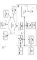
一実施形態において、プラズマ処理システムは、プラズマ処理装置1及び制御部2を含む。プラズマ処理システムは、基板処理システムの一例であり、プラズマ処理装置1は、基板処理装置の一例である。プラズマ処理装置1は、プラズマ処理チャンバ10、基板支持部11及びプラズマ生成部12を含む。プラズマ処理チャンバ10は、プラズマ処理空間を有する。また、プラズマ処理チャンバ10は、少なくとも1つの処理ガスをプラズマ処理空間に供給するための少なくとも1つのガス供給口と、プラズマ処理空間からガスを排出するための少なくとも1つのガス排出口とを有する。ガス供給口は、後述するガス供給部20に接続され、ガス排出口は、後述する排気システム40に接続される。基板支持部11は、プラズマ処理空間内に配置され、基板を支持するための基板支持面及びエッジリングを支持するためのリング支持面を有する。
In one embodiment, the plasma processing system includes a plasma processing apparatus 1 and a controller 2. The plasma processing system is an example of a substrate processing system, and the plasma processing apparatus 1 is an example of a substrate processing apparatus. The plasma processing apparatus 1 includes a plasma processing chamber 10 , a substrate support section 11 and a plasma generation section 12 . Plasma processing chamber 10 has a plasma processing space. The plasma processing chamber 10 also has at least one gas inlet for supplying at least one process gas to the plasma processing space and at least one gas outlet for exhausting gas from the plasma processing space. The gas supply port is connected to a gas supply section 20, which will be described later, and the gas discharge port is connected to an exhaust system 40, which will be described later. The substrate support 11 is arranged in the plasma processing space and has a substrate support surface for supporting the substrate and a ring support surface for supporting the edge ring.
プラズマ生成部12は、プラズマ処理空間内に供給された少なくとも1つの処理ガスからプラズマを生成するように構成される。プラズマ処理空間において形成されるプラズマは、容量結合プラズマ(CCP:Capacitively Coupled Plasma)、誘導結合プラズマ(ICP:Inductively Coupled Plasma)、ECRプラズマ(Electron-Cyclotron-resonance plasma)、ヘリコン波励起プラズマ(HWP:Helicon Wave Plasma)、又は、表面波プラズマ(SWP:Surface Wave Plasma)等であってもよい。また、AC(Alternating Current)プラズマ生成部及びDC(Direct Current)プラズマ生成部を含む、種々のタイプのプラズマ生成部が用いられてもよい。一実施形態において、ACプラズマ生成部で用いられるAC信号(AC電力)は、100kHz~10GHzの範囲内の周波数を有する。従って、AC信号は、RF(Radio Frequency)信号及びマイクロ波信号を含む。一実施形態において、RF信号は、100kHz~150MHzの範囲内の周波数を有する。
The plasma generation unit 12 is configured to generate plasma from at least one processing gas supplied into the plasma processing space. Plasma formed in the plasma processing space includes capacitively coupled plasma (CCP: Capacitively Coupled Plasma), inductively coupled plasma (ICP: Inductively Coupled Plasma), ECR plasma (Electron-Cyclotron-resonance plasma), helicon wave excited plasma (HWP: Helicon Wave Plasma), surface wave plasma (SWP: Surface Wave Plasma), or the like. Various types of plasma generators may also be used, including alternating current (AC) plasma generators and direct current (DC) plasma generators. In one embodiment, the AC signal (AC power) used in the AC plasma generator has a frequency within the range of 100 kHz to 10 GHz. Therefore, AC signals include RF (Radio Frequency) signals and microwave signals. In one embodiment, the RF signal has a frequency within the range of 100 kHz-150 MHz.
制御部2は、本開示において述べられる種々の工程をプラズマ処理装置1に実行させるコンピュータ実行可能な命令を処理する。制御部2は、ここで述べられる種々の工程を実行するようにプラズマ処理装置1の各要素を制御するように構成され得る。一実施形態において、制御部2の一部又は全てがプラズマ処理装置1に含まれてもよい。制御部2は、処理部2a1、記憶部2a2及び通信インターフェース2a3を含んでもよい。制御部2は、例えばコンピュータ2aにより実現される。処理部2a1は、記憶部2a2からプログラムを読み出し、読み出されたプログラムを実行することにより種々の制御動作を行うように構成され得る。このプログラムは、予め記憶部2a2に格納されていてもよく、必要なときに、媒体を介して取得されてもよい。取得されたプログラムは、記憶部2a2に格納され、処理部2a1によって記憶部2a2から読み出されて実行される。媒体は、コンピュータ2aに読み取り可能な種々の記憶媒体であってもよく、通信インターフェース2a3に接続されている通信回線であってもよい。処理部2a1は、CPU(Central Processing Unit)であってもよい。記憶部2a2は、RAM(Random Access Memory)、ROM(Read Only Memory)、HDD(Hard Disk Drive)、SSD(Solid State Drive)、又はこれらの組み合わせを含んでもよい。通信インターフェース2a3は、LAN(Local Area Network)等の通信回線を介してプラズマ処理装置1との間で通信してもよい。また、上記記憶媒体は、一時的なものであっても非一時的なものであってもよい。
The controller 2 processes computer-executable instructions that cause the plasma processing apparatus 1 to perform the various steps described in this disclosure. Controller 2 may be configured to control elements of plasma processing apparatus 1 to perform the various processes described herein. In one embodiment, part or all of the controller 2 may be included in the plasma processing apparatus 1 . The control unit 2 may include a processing unit 2a1, a storage unit 2a2, and a communication interface 2a3. The control unit 2 is implemented by, for example, a computer 2a. Processing unit 2a1 can be configured to perform various control operations by reading a program from storage unit 2a2 and executing the read program. This program may be stored in the storage unit 2a2 in advance, or may be acquired via a medium when necessary. The acquired program is stored in the storage unit 2a2, read from the storage unit 2a2 and executed by the processing unit 2a1. The medium may be various storage media readable by the computer 2a, or may be a communication line connected to the communication interface 2a3. The processing unit 2a1 may be a CPU (Central Processing Unit). The storage unit 2a2 may include RAM (Random Access Memory), ROM (Read Only Memory), HDD (Hard Disk Drive), SSD (Solid State Drive), or a combination thereof. The communication interface 2a3 may communicate with the plasma processing apparatus 1 via a communication line such as a LAN (Local Area Network). Moreover, the storage medium may be temporary or non-temporary.
<制御部または制御回路>
図2は、本明細書に記載された種々の実施形態を実装し得るコンピュータのブロック図である。本開示の制御態様は、システム、方法、および/またはコンピュータプログラム製品として具現化され得る。コンピュータプログラム製品は、コンピュータ読み取り可能なプログラム命令が記録されたコンピュータ読み取り可能な記憶媒体を含み、1つ以上のプロセッサが実施形態の態様を実行する可能性がある。 <Control unit or control circuit>
FIG. 2 is a block diagram of a computer that may implement various embodiments described herein. Control aspects of the present disclosure may be embodied as systems, methods, and/or computer program products. The computer program product includes a computer-readable storage medium having computer-readable program instructions recorded thereon, and one or more processors may implement aspects of the embodiments.
コンピュータ読み取り可能な記憶媒体は、命令実行装置(プロセッサ)による使用命令を記憶できる有形装置であってもよい。コンピュータ読み取り可能な記憶媒体としては、例えば電子記憶装置、磁気記憶装置、光記憶装置、電磁記憶装置、半導体記憶装置、またはこれらの装置の任意の適切な組み合わせが挙げられるが、これらに限定されない。コンピュータ読み取り可能な記憶媒体(および適切な組み合わせ)のより具体的な例の非網羅的なリストには、次の各々が含まれる:フレキシブルディスク、ハードディスク、ソリッドステートドライブ(SSD)、ランダムアクセスメモリ(RAM)、読み取り専用メモリ(ROM)、プログラム可能な読み取り専用メモリ(EPROMまたはフラッシュ)、静的ランダムアクセスメモリ(SRAM)、コンパクトディスク(CDまたはCD-ROM)、デジタル汎用ディスク(DVD)、メモリカードまたはスティック。本開示で用いられているコンピュータ読み取り可能な記憶媒体は、電波や他の自由に伝播する電磁波、導波路やその他の伝送媒体(例えば、光ファイバケーブルを通過する光パルス)を介して伝播する電磁波、または電線を通る電気信号など、それ自身が一時的な信号であると解釈されるべきではない。
A computer-readable storage medium may be a tangible device capable of storing instructions for use by an instruction execution device (processor). Computer-readable storage media include, but are not limited to, electronic storage devices, magnetic storage devices, optical storage devices, electromagnetic storage devices, semiconductor storage devices, or any suitable combination of these devices. A non-exhaustive list of more specific examples of computer-readable storage media (and suitable combinations) include each of the following: floppy disk, hard disk, solid state drive (SSD), random access memory ( RAM), Read Only Memory (ROM), Programmable Read Only Memory (EPROM or Flash), Static Random Access Memory (SRAM), Compact Disc (CD or CD-ROM), Digital Versatile Disc (DVD), Memory Card Or stick. Computer-readable storage media as used in this disclosure include radio waves and other freely propagating electromagnetic waves, electromagnetic waves propagating through waveguides and other transmission media (e.g., light pulses passing through fiber optic cables). , or an electrical signal through a wire, etc. itself should not be construed as a transitory signal.
本開示に記載されたコンピュータ読み取り可能なプログラム命令は、コンピュータ読み取り可能な記憶媒体から、またはグローバルネットワーク(すなわち、インターネット)、ローカルエリアネットワーク、広域ネットワークおよび/または無線ネットワークを介して外部コンピュータまたは外部記憶装置に適切なコンピューティングデバイスまたは処理デバイスにダウンロードすることができる。ネットワークには、銅線、光通信ファイバ、無線伝送、ルーター、ファイアウォール、スイッチ、ゲートウェイコンピュータ、エッジサーバが含まれる場合がある。各コンピューティングデバイスまたは処理デバイスのネットワークアダプタカードまたはネットワークインターフェースは、コンピュータ読み取り可能なプログラム命令をネットワークから受信し、コンピュータ読み取り可能なプログラム命令を、コンピューティングデバイスまたは処理デバイス内のコンピュータの読み取り可能な記憶媒体に格納するために転送してもよい。
The computer-readable program instructions described in this disclosure can be transferred from a computer-readable storage medium or to an external computer or storage via a global network (i.e., the Internet), local area network, wide area network and/or wireless network. It can be downloaded to a suitable computing or processing device for the apparatus. Networks may include copper wires, optical fiber, wireless transmissions, routers, firewalls, switches, gateway computers, and edge servers. A network adapter card or network interface in each computing or processing device receives computer readable program instructions from the network and stores the computer readable program instructions in computer readable storage within the computing or processing device. May be transferred for storage on media.
本開示の操作を実行するためのコンピュータ読み取り可能なプログラム命令は、機械語命令および/またはマイクロコードを含み、アセンブリ言語、Basic、Fortran、Java、Python、R、C、C++、C#または同様のプログラミング言語を含む1つ以上のプログラミング言語の任意の組み合わせで記述されたソースコードからコンパイルまたはインタープリットすることができる。コンピュータの読み取り可能なプログラム命令は、ユーザのパーソナルコンピュータ、ノートブックコンピュータ、タブレット、またはスマートフォン上で完全に実行されてもよいし、リモートコンピュータまたはコンピュータサーバ上で、またはこれらのコンピューティングデバイスの任意の組み合わせで完全に実行されてもよい。リモートコンピュータまたはコンピュータサーバは、ローカルエリアネットワークやワイドエリアネットワーク、またはグローバルネットワーク(インターネット)を含むコンピュータネットワークを介して、ユーザのデバイスまたはデバイスに接続することができる。いくつかの実施形態では、電子回路は、例えば、プログラマブル論理回路、フィールドプログラマブルゲートアレイ(FPGA)、またはプログラマブルロジックアレイ(PLA)を含む、コンピュータ読み取り可能なプログラム命令からの情報を使用してコンピュータ読み取り可能なプログラム命令を実行して電子回路を構成またはカスタマイズし、本開示の態様を実行する。
Computer readable program instructions for performing the operations of the present disclosure include machine language instructions and/or microcode and may be written in assembly language, Basic, Fortran, Java, Python, R, C, C++, C# or similar. It can be compiled or interpreted from source code written in any combination of one or more programming languages, including programming languages. The computer readable program instructions may be executed entirely on a user's personal computer, notebook computer, tablet, or smart phone, or on a remote computer or computer server, or any of these computing devices. It may also be fully implemented in combination. The remote computer or computer server may be connected to the user's device or devices via computer networks, including local area networks, wide area networks, or global networks (the Internet). In some embodiments, electronic circuits are computer readable using information from computer readable program instructions, including, for example, programmable logic circuits, field programmable gate arrays (FPGAs), or programmable logic arrays (PLAs). Execute possible program instructions to configure or customize the electronic circuitry to carry out aspects of the present disclosure.
本開示の態様は、開示の実施形態にかかる方法のフロー図およびブロック図、装置(システム)、およびコンピュータプログラム製品を参照して説明する。フロー図とブロック図の各ブロック、およびフロー図およびブロック図におけるブロックの組み合わせは、コンピュータ読み取り可能なプログラム命令によって実現できることを当業者は理解する。
Aspects of the present disclosure are described with reference to flowchart illustrations and block diagrams of methods, apparatus (systems), and computer program products according to embodiments of the disclosure. Persons of ordinary skill in the art will understand that each block of the flowchart illustrations and block diagrams, and combinations of blocks in the flowchart illustrations and block diagrams, can be implemented by computer readable program instructions.
本開示に記載されたシステムおよび方法を実装することができるコンピュータ読み取り可能なプログラム命令は、汎用コンピュータ、特殊目的コンピュータ、または他のプログラマブル装置の1つ以上のプロセッサ(および/またはプロセッサ内の1つ以上のコア)に提供され得る。これらのコンピュータ読み取り可能なプログラム命令は、コンピュータ、プログラマブル装置、および/または他のデバイスが特定の方法で機能するように指示することができるコンピュータ読み取り可能な記憶媒体に格納されてもよく、その場合、その指示を格納しているコンピュータ読み取り可能な記憶媒体は、本開示のフロー図およびブロック図で指定された機能の態様を実装する命令を含む製品である。
Computer readable program instructions with which the systems and methods described in this disclosure can be implemented are stored in one or more processors (and/or one within a processor) of a general purpose computer, special purpose computer, or other programmable device. above core). These computer-readable program instructions may be stored on a computer-readable storage medium capable of directing a computer, programmable apparatus, and/or other device to function in a particular manner, where , a computer-readable storage medium having instructions stored thereon, is an article of manufacture that includes instructions for implementing aspects of the functionality specified in the flow diagrams and block diagrams of this disclosure.
また、コンピュータ読み取り可能なプログラム命令は、コンピュータ、他のプログラム可能な装置、または他の装置にロードされてもよく、コンピュータ、他のプログラム可能な装置、または他の装置上で実行される命令が、本開示のフロー図およびブロック図で指定された機能を実装するように、一連の動作ステップを実行させてコンピュータ実装プロセスを生成してもよい。
Also, the computer-readable program instructions may be loaded into a computer, other programmable device, or other device, such that the instructions executed on the computer, other programmable device, or other device , may generate a computer-implemented process by performing a series of operational steps to implement the functions specified in the flow diagrams and block diagrams of this disclosure.
図2は、1台または複数台のネットワーク化されたコンピュータおよびサーバのネットワーク化システム800を示す機能ブロック図である。一実施形態において、図2に示すハードウェアおよびソフトウェア環境は、本開示にかかるソフトウェアおよび/または方法の実装のための例示的なプラットフォームを提供し得る。
FIG. 2 is a functional block diagram illustrating a networking system 800 of one or more networked computers and servers. In one embodiment, the hardware and software environment shown in FIG. 2 may provide an exemplary platform for implementation of software and/or methods according to this disclosure.
図2に示されるように、ネットワーク化システム800は、コンピュータ805、ネットワーク810、リモートコンピュータ815、ウェブサーバ820、クラウドストレージサーバ825およびコンピュータサーバ830を含んでいてもよいが、これらに限定されない。いくつかの実施形態では、図2に示す1つ以上の機能ブロックの複数のインスタンスが採用されてもよい。
As shown in FIG. 2, networked system 800 may include, but is not limited to, computer 805, network 810, remote computer 815, web server 820, cloud storage server 825 and computer server 830. In some embodiments, multiple instances of one or more of the functional blocks shown in FIG. 2 may be employed.
コンピュータ805の追加詳細を図2に示す。コンピュータ805内に示される機能ブロックは、例示的な機能を確立するためにのみ提供され、網羅的であることを意図したものではない。また、リモートコンピュータ815、ウェブサーバ820、クラウドストレージサーバ825およびコンピュータサーバ830については詳細が提供されていないが、これらの他のコンピュータおよびデバイスは、コンピュータ805に対して示される同様の機能を備えてもよい。
Additional details of computer 805 are shown in FIG. The functional blocks depicted within computer 805 are provided to establish exemplary functionality only and are not intended to be exhaustive. Also, although no details are provided for remote computer 815, web server 820, cloud storage server 825 and computer server 830, these other computers and devices have similar functionality shown for computer 805. good too.
コンピュータ805は、パーソナルコンピュータ(PC)、デスクトップコンピュータ、ラップトップコンピュータ、タブレットコンピュータ、ネットブックコンピュータ、パーソナルデジタルアシスタント(PDA)、スマートフォン、またはネットワーク810上の他のデバイスと通信できる任意の他のプログラマブル電子装置とすることができる。
Computer 805 may be a personal computer (PC), desktop computer, laptop computer, tablet computer, netbook computer, personal digital assistant (PDA), smart phone, or any other programmable electronic device capable of communicating with other devices on network 810. can be a device.
コンピュータ805は、プロセッサ835、バス837、メモリ840、不揮発性ストレージ845、ネットワークインターフェース850、周辺インターフェース855およびディスプレイインターフェース865を含み得る。これらの各機能は、いくつかの実施形態において、個々の電子サブシステム(集積回路チップまたはチップと関連するデバイスの組み合わせ)として、または、他の実施形態において、ある程度の機能の組み合わせが、単一のチップ(チップオンシステムまたはSoCと呼ばれる場合がある)上に実装され得る。
Computer 805 may include processor 835 , bus 837 , memory 840 , nonvolatile storage 845 , network interface 850 , peripherals interface 855 and display interface 865 . Each of these functions may be implemented in some embodiments as individual electronic subsystems (an integrated circuit chip or combination of chips and associated devices), or in other embodiments some combination of functions may be implemented in a single on a chip (sometimes called a chip-on-system or SoC).
プロセッサ835は、インテルコーポレーション、アドバンストマイクロデバイス社(AMD)、アームホールディングス(アーム)、アップルコンピュータなどによって設計および/または製造されたものなど、1つまたは複数のシングルまたはマルチチップマイクロプロセッサであってもよい。マイクロプロセッサの例としては、インテル社のセレロン、ペンティウム、コアi3、コアi5及びコアi7、AMDのオプテロン、フェノム、アスロン、トゥリオン及びライゼン、アームのコーテックス-A、コーテックス-R及びコーテックス-Mなどがある。
Processor 835 may be one or more single or multi-chip microprocessors, such as those designed and/or manufactured by Intel Corporation, Advanced Micro Devices, Inc. (AMD), Arm Holdings (Arm), Apple Computer, etc. good. Examples of microprocessors include Celeron, Pentium, Core i3, Core i5 and Core i7 from Intel, Opteron, Phenom, Athlon, Turion and Risen from AMD, Cortex-A, Cortex-R and Cortex- from AMD. There are M.
バス837は、ISA、PCI、PCIExpress(PCI-e)、AGPなどの独自の標準の高速パラレルまたはシリアルペリフェラルインターコネクトバスとすることができる。
Bus 837 can be any proprietary standard high speed parallel or serial peripheral interconnect bus such as ISA, PCI, PCI Express (PCI-e), AGP, or the like.
メモリ840および不揮発性ストレージ845は、コンピュータ読み取り可能な記憶媒体とすることができる。メモリ840は、ダイナミックランダムアクセスメモリ(DRAM)および静的ランダムアクセスメモリ(SRAM)などの任意の適切な揮発性記憶装置を含んでいてもよい。不揮発性ストレージ845は、フレキシブルディスク、ハードディスク、ソリッドステートドライブ(SSD)、読み取り専用メモリ(ROM)、プログラム可能な読み取り専用メモリ(EPROMまたはFlash)、コンパクトディスク(CDまたはCD-ROM)、デジタル汎用ディスク(DVD)およびメモリカードまたはスティックの1つ以上を含むことができる。
Memory 840 and non-volatile storage 845 can be computer-readable storage media. Memory 840 may include any suitable volatile storage such as dynamic random access memory (DRAM) and static random access memory (SRAM). Non-volatile storage 845 can be floppy disk, hard disk, solid state drive (SSD), read only memory (ROM), programmable read only memory (EPROM or Flash), compact disk (CD or CD-ROM), digital general purpose disk. (DVD) and one or more of memory cards or sticks.
プログラム848は、不揮発性ストレージ845に格納され、本開示の他の場所で詳細に説明され、かつ図面に示されている特定のソフトウェア機能を作成、管理、および制御するために使用される機械読み取り可能な命令および/またはデータの集合であってもよい。いくつかの実施形態では、メモリ840は、不揮発性ストレージ845よりもかなり速くてもよい。このような実施形態では、プログラム848は、プロセッサ835によって実行される前に不揮発性ストレージ845からメモリ840に転送されてもよい。
Programs 848 are machine-readable programs stored in nonvolatile storage 845 and used to create, manage, and control certain software functions that are described in detail elsewhere in this disclosure and illustrated in the drawings. It may be a set of possible instructions and/or data. In some embodiments, memory 840 may be significantly faster than non-volatile storage 845 . In such embodiments, programs 848 may be transferred from nonvolatile storage 845 to memory 840 before being executed by processor 835 .
コンピュータ805は、ネットワークインターフェース850を介してネットワーク810を介して他のコンピュータと通信し、対話することができる。ネットワーク810は、例えば、ローカルエリアネットワーク(LAN)、インターネット等の広域ネットワーク(WAN)、または両者の組み合わせ、有線、無線、または光ファイバ接続を含んでもよい。一般に、ネットワーク810は、2台以上のコンピュータと関連するデバイス間の通信をサポートする接続およびプロトコルの任意の組み合わせであり得る。
Computer 805 can communicate and interact with other computers over network 810 via network interface 850 . Network 810 may include, for example, a local area network (LAN), a wide area network (WAN) such as the Internet, or a combination of both, wired, wireless, or fiber optic connections. In general, network 810 can be any combination of connections and protocols that support communication between two or more computers and associated devices.
周辺インターフェース855は、コンピュータ805とローカルに接続されてもよい他の装置とのデータの入出力を可能にし得る。例えば、周辺インターフェース855は、外部デバイス860への接続を提供することができる。外部デバイス860は、キーボード、マウス、キーパッド、タッチスクリーン、および/または他の適切な入力デバイスなどのデバイスを含んでいてもよい。外部デバイス860はまた、例えばサムドライブ、ポータブル光ディスクまたは磁気ディスク、およびメモリカードのようなポータブルコンピュータ読み取り可能な記憶媒体を含むことができる。本開示の実施形態に用いるソフトウェアおよびデータは、例えば、プログラム848、携帯型コンピュータ読み取り可能な記憶媒体などに記憶され得る。このような実施形態では、ソフトウェアは、不揮発性ストレージ845にロードされるか、あるいは、代わりに、周辺インターフェース855を介してメモリ840に直接ロードされ得る。周辺インターフェース855は、RS-232やユニバーサルシリアルバス(USB)などの業界標準接続を使用して外部デバイス860と接続することができる。
Peripherals interface 855 may allow input and output of data with other devices that may be locally connected to computer 805 . For example, peripherals interface 855 may provide connectivity to external devices 860 . External devices 860 may include devices such as keyboards, mice, keypads, touch screens, and/or other suitable input devices. External devices 860 may also include portable computer-readable storage media such as, for example, thumb drives, portable or magnetic disks, and memory cards. Software and data used in embodiments of the present disclosure may be stored, for example, in program 848, portable computer-readable storage media, and the like. In such embodiments, the software may be loaded into non-volatile storage 845 or, alternatively, loaded directly into memory 840 via peripheral interface 855 . Peripheral interface 855 may connect to external devices 860 using industry standard connections such as RS-232 or Universal Serial Bus (USB).
ディスプレイインターフェース865は、コンピュータ805をディスプレイ870に接続してもよい。ディスプレイ870は、いくつかの実施形態において、コンピュータ805のユーザにコマンドラインまたはグラフィカルユーザインタフェースを提示するために使用され得る。ディスプレイインターフェース865は、1つ以上の独自仕様の接続、またはVGA、DVI、ディスプレイポート、HDMI(登録商標)などの業界標準接続を使用してディスプレイ870に接続することができる。
A display interface 865 may connect the computer 805 to the display 870 . Display 870 may be used in some embodiments to present a command line or graphical user interface to a user of computer 805 . Display interface 865 may connect to display 870 using one or more proprietary or industry standard connections such as VGA, DVI, DisplayPort, HDMI.
上記したように、ネットワークインターフェース850は、コンピュータ805外部の他のコンピューティングシステムおよびストレージシステムまたはデバイスとの通信を提供する。本明細書で説明するソフトウェアプログラムおよびデータは、例えば、リモートコンピュータ815、ウェブサーバ820、クラウドストレージサーバ825およびコンピュータサーバ830から、ネットワークインターフェース850およびネットワーク810を介して不揮発性ストレージ845にダウンロードされ得る。さらに、本開示に記載されたシステムおよび方法は、ネットワークインターフェース850およびネットワーク810を介してコンピュータ805に接続された1台以上のコンピュータによって実行され得る。例えば、いくつかの実施形態では、本開示に記載されたシステムおよび方法は、リモートコンピュータ815、コンピュータサーバ830、またはネットワーク810上の相互接続されたコンピュータの組み合わせによって実行され得る。
As noted above, network interface 850 provides communication with other computing and storage systems or devices external to computer 805 . The software programs and data described herein may be downloaded to non-volatile storage 845 via network interface 850 and network 810 from remote computers 815 , web servers 820 , cloud storage servers 825 and computer servers 830 , for example. Additionally, the systems and methods described in this disclosure can be performed by one or more computers connected to computer 805 via network interface 850 and network 810 . For example, in some embodiments, the systems and methods described in this disclosure may be performed by remote computer 815 , computer server 830 , or a combination of interconnected computers on network 810 .
データ、データセットおよび/または本開示に記載されたシステムおよび方法の実施の実施例で用いられたデータベースは、リモートコンピュータ815、ウェブサーバ820、クラウドストレージサーバ825およびコンピュータサーバ830から保存またはダウンロードされ得る。
Data, datasets and/or databases used in examples of implementation of the systems and methods described in this disclosure may be stored or downloaded from remote computers 815, web servers 820, cloud storage servers 825 and computer servers 830. .
<プラズマ処理装置>
次に、上記したプラズマ処理装置1の一例として、容量結合型のプラズマ処理装置1の構成例について説明する。図3は、プラズマ処理装置1の構成例を説明するための図である。 <Plasma processing device>
Next, a configuration example of a capacitively coupledplasma processing apparatus 1 will be described as an example of the plasma processing apparatus 1 described above. FIG. 3 is a diagram for explaining a configuration example of the plasma processing apparatus 1. As shown in FIG.
次に、上記したプラズマ処理装置1の一例として、容量結合型のプラズマ処理装置1の構成例について説明する。図3は、プラズマ処理装置1の構成例を説明するための図である。 <Plasma processing device>
Next, a configuration example of a capacitively coupled
プラズマ処理装置1は、プラズマ処理チャンバ10、ガス供給部20、電源30及び排気システム40を含む。また、プラズマ処理装置1は、基板支持器の一例としての基板支持部11及びガス導入部を含む。基板支持部11は、プラズマ処理チャンバ10内に配置される。ガス導入部は、少なくとも1つの処理ガスをプラズマ処理チャンバ10内に導入するように構成される。ガス導入部は、シャワーヘッド13を含む。シャワーヘッド13は、基板支持部11の上方に配置される。一実施形態において、シャワーヘッド13は、プラズマ処理チャンバ10の天部(ceiling)の少なくとも一部を構成する。プラズマ処理チャンバ10の内部には、シャワーヘッド13、プラズマ処理チャンバ10の側壁10a及び基板支持部11により規定されたプラズマ処理空間10sが形成される。プラズマ処理チャンバ10は接地される。シャワーヘッド13及び基板支持部11は、プラズマ処理チャンバ10の筐体とは電気的に絶縁される。
The plasma processing apparatus 1 includes a plasma processing chamber 10, a gas supply section 20, a power supply 30 and an exhaust system 40. The plasma processing apparatus 1 also includes a substrate supporter 11 as an example of a substrate supporter and a gas inlet. A substrate support 11 is positioned within the plasma processing chamber 10 . The gas introduction is configured to introduce at least one process gas into the plasma processing chamber 10 . The gas introduction section includes a showerhead 13 . The showerhead 13 is arranged above the substrate support 11 . In one embodiment, showerhead 13 forms at least a portion of the ceiling of plasma processing chamber 10 . Inside the plasma processing chamber 10, a plasma processing space 10s defined by the shower head 13, the side wall 10a of the plasma processing chamber 10, and the substrate support 11 is formed. Plasma processing chamber 10 is grounded. The showerhead 13 and substrate support 11 are electrically insulated from the housing of the plasma processing chamber 10 .
基板支持部11は、本体部110及びリングアセンブリ120を含む。本体部110は、基板Wを支持するための中央領域110aと、リングアセンブリ120を支持するための環状領域110bとを有する。ウェハは基板Wの一例である。本体部110の環状領域110bは、平面視で本体部110の中央領域110aを囲んでいる。基板Wは、本体部110の中央領域110a上に配置され、リングアセンブリ120は、本体部110の中央領域110a上の基板Wを囲むように本体部110の環状領域110b上に配置される。従って、中央領域110aは、基板Wを支持するための基板支持面とも呼ばれ、環状領域110bは、リングアセンブリ120を支持するためのリング支持面とも呼ばれる。
The substrate support section 11 includes a main body section 110 and a ring assembly 120 . Body portion 110 has a central region 110 a for supporting substrate W and an annular region 110 b for supporting ring assembly 120 . A wafer is an example of a substrate W; The annular region 110b of the body portion 110 surrounds the central region 110a of the body portion 110 in plan view. The substrate W is placed on the central region 110 a of the body portion 110 , and the ring assembly 120 is placed on the annular region 110 b of the body portion 110 so as to surround the substrate W on the central region 110 a of the body portion 110 . Accordingly, the central region 110a is also referred to as a substrate support surface for supporting the substrate W, and the annular region 110b is also referred to as a ring support surface for supporting the ring assembly 120. FIG.
また、一実施形態において本体部110は、導電性基台111、静電チャック112及び環状静電チャック113を含む。
Also, in one embodiment, the body portion 110 includes a conductive base 111 , an electrostatic chuck 112 and an annular electrostatic chuck 113 .
導電性基台111は、アルミニウムなどの導電性部材を含み、略円板形状を有している。導電性基台111の導電性部材は下部電極として機能し得る。
静電チャック112は、導電性基台111の上に配置される。静電チャック112は、セラミック部材112aと、セラミック部材112a内に配置される複数の電極114と、セラミック部材112a内に形成される伝熱ガス供給部115を含む(図4を参照)。セラミック部材112aは、中央領域110aを有する。
環状静電チャック113は、導電性基台111の上において静電チャック112を囲むように配置される。環状静電チャック113は、セラミック部材113aと、セラミック部材113a内に配置される複数の電極116と、セラミック部材113a内に形成される伝熱ガス供給部117を含む(図4を参照)。セラミック部材113aは、環状領域110bを有する。環状静電チャック113は、図示のように導電性基台111の上で静電チャック112と一体に形成されてもよく、又は独立して(分離して)形成されてもよい。 Theconductive base 111 includes a conductive member such as aluminum and has a substantially disk shape. The conductive member of the conductive base 111 can function as a lower electrode.
Theelectrostatic chuck 112 is arranged on the conductive base 111 . The electrostatic chuck 112 includes a ceramic member 112a, a plurality of electrodes 114 disposed within the ceramic member 112a, and a heat transfer gas supply 115 formed within the ceramic member 112a (see FIG. 4). Ceramic member 112a has a central region 110a.
The annularelectrostatic chuck 113 is arranged on the conductive base 111 so as to surround the electrostatic chuck 112 . The annular electrostatic chuck 113 includes a ceramic member 113a, a plurality of electrodes 116 disposed within the ceramic member 113a, and a heat transfer gas supply 117 formed within the ceramic member 113a (see FIG. 4). Ceramic member 113a has an annular region 110b. The annular electrostatic chuck 113 may be integrally formed with the electrostatic chuck 112 on the conductive base 111 as shown, or may be formed independently (separately).
静電チャック112は、導電性基台111の上に配置される。静電チャック112は、セラミック部材112aと、セラミック部材112a内に配置される複数の電極114と、セラミック部材112a内に形成される伝熱ガス供給部115を含む(図4を参照)。セラミック部材112aは、中央領域110aを有する。
環状静電チャック113は、導電性基台111の上において静電チャック112を囲むように配置される。環状静電チャック113は、セラミック部材113aと、セラミック部材113a内に配置される複数の電極116と、セラミック部材113a内に形成される伝熱ガス供給部117を含む(図4を参照)。セラミック部材113aは、環状領域110bを有する。環状静電チャック113は、図示のように導電性基台111の上で静電チャック112と一体に形成されてもよく、又は独立して(分離して)形成されてもよい。 The
The
The annular
セラミック部材112a、113a内には、後述するRF電源31及び/又はDC電源32に結合される、少なくとも1つのRF/DC電極が配置されてもよい。少なくとも1つのRF/DC電極は、上記した複数の電極114、複数の電極116に相当し得る。この場合、少なくとも1つのRF/DC電極が下部電極として機能する。後述するバイアスRF信号及び/又はDC信号が少なくとも1つのRF/DC電極に供給される場合、RF/DC電極はバイアス電極とも呼ばれる。なお、導電性基台111の導電性部材と少なくとも1つのRF/DC電極とが複数の下部電極として機能してもよい。また、静電電極が下部電極として機能してもよい。従って、基板支持部11は、少なくとも1つの下部電極を含む。
At least one RF/DC electrode coupled to an RF power supply 31 and/or a DC power supply 32, which will be described later, may be arranged in the ceramic members 112a, 113a. The at least one RF/DC electrode may correspond to the plurality of electrodes 114, plurality of electrodes 116 described above. In this case, at least one RF/DC electrode functions as the bottom electrode. If a bias RF signal and/or a DC signal, described below, is applied to at least one RF/DC electrode, the RF/DC electrode is also called a bias electrode. The conductive member of the conductive base 111 and at least one RF/DC electrode may function as a plurality of lower electrodes. Alternatively, the electrostatic electrode may function as the lower electrode. Accordingly, the substrate support 11 includes at least one bottom electrode.
リングアセンブリ120は、1又は複数の環状部材を含む。一実施形態において、1又は複数の環状部材は、1又は複数のエッジリングを含む。また。1又は複数の環状部材は、少なくとも1つのカバーリングを含んでいてもよい。エッジリングは、導電性材料又は絶縁材料で形成され、カバーリングは、絶縁材料で形成される。
リングアセンブリ120は、環状静電チャック113の上に配置されてもよく、静電チャック112と環状静電チャック113の両方の上に配置されてもよい。Ring assembly 120 includes one or more annular members. In one embodiment, the one or more annular members include one or more edge rings. again. The one or more annular members may include at least one cover ring. The edge ring is made of a conductive material or an insulating material, and the cover ring is made of an insulating material.
Ring assembly 120 may be positioned over annular electrostatic chuck 113 or may be positioned over both electrostatic chuck 112 and annular electrostatic chuck 113 .
リングアセンブリ120は、環状静電チャック113の上に配置されてもよく、静電チャック112と環状静電チャック113の両方の上に配置されてもよい。
また基板支持部11は、静電チャック112、環状静電チャック113、リングアセンブリ120及び基板Wのうち少なくとも1つをターゲット温度に調節するように構成される温調モジュールを含んでもよい。温調モジュールは、ヒータ、伝熱媒体、流路111a、又はこれらの組み合わせを含んでもよい。流路111aには、ブラインやガスのような伝熱流体が流れる。一実施形態において、流路111aが導電性基台111内に形成され、1又は複数のヒータが静電チャック112、環状静電チャック113のセラミック部材112a、113a内に配置される。なお、温調モジュールの構成はこれに限定されるものではなく、静電チャック112、環状静電チャック113、リングアセンブリ120及び基板Wのうち少なくとも1つの温度を調整できるように構成されればよい。
The substrate supporter 11 may also include a temperature control module configured to adjust at least one of the electrostatic chuck 112, the annular electrostatic chuck 113, the ring assembly 120, and the substrate W to a target temperature. The temperature control module may include heaters, heat transfer media, flow channels 111a, or combinations thereof. A heat transfer fluid such as brine or gas flows through the flow path 111a. In one embodiment, a channel 111a is formed in the conductive base 111 and one or more heaters are positioned in the ceramic members 112a, 113a of the electrostatic chuck 112, the annular electrostatic chuck 113, and the like. Note that the configuration of the temperature control module is not limited to this, and may be configured to adjust the temperature of at least one of the electrostatic chuck 112, the annular electrostatic chuck 113, the ring assembly 120, and the substrate W. .
なお、基板支持部11の詳細な構成については後述する。
A detailed configuration of the substrate support portion 11 will be described later.
シャワーヘッド13は、ガス供給部20からの少なくとも1つの処理ガスをプラズマ処理空間10s内に導入するように構成される。シャワーヘッド13は、少なくとも1つのガス供給口13a、少なくとも1つのガス拡散室13b、及び複数のガス導入口13cを有する。ガス供給口13aに供給された処理ガスは、ガス拡散室13bを通過して複数のガス導入口13cからプラズマ処理空間10s内に導入される。また、シャワーヘッド13は、少なくとも1つの上部電極を含む。なお、ガス導入部は、シャワーヘッド13に加えて、側壁10aに形成された1又は複数の開口部に取り付けられる1又は複数のサイドガス注入部(SGI:Side Gas Injector)を含んでもよい。
The showerhead 13 is configured to introduce at least one processing gas from the gas supply unit 20 into the plasma processing space 10s. The showerhead 13 has at least one gas supply port 13a, at least one gas diffusion chamber 13b, and multiple gas introduction ports 13c. The processing gas supplied to the gas supply port 13a passes through the gas diffusion chamber 13b and is introduced into the plasma processing space 10s through a plurality of gas introduction ports 13c. Showerhead 13 also includes at least one upper electrode. In addition to the showerhead 13, the gas introduction part may include one or more side gas injectors (SGI: Side Gas Injector) attached to one or more openings formed in the side wall 10a.
ガス供給部20は、少なくとも1つのガスソース21及び少なくとも1つの流量制御器22を含んでもよい。一実施形態において、ガス供給部20は、少なくとも1つの処理ガスを、それぞれに対応のガスソース21からそれぞれに対応の流量制御器22を介してシャワーヘッド13に供給するように構成される。各流量制御器22は、例えばマスフローコントローラ又は圧力制御式の流量制御器を含んでもよい。さらに、ガス供給部20は、少なくとも1つの処理ガスの流量を変調又はパルス化する少なくとも1つの流量変調デバイスを含んでもよい。
The gas supply unit 20 may include at least one gas source 21 and at least one flow controller 22 . In one embodiment, gas supply 20 is configured to supply at least one process gas from respective gas sources 21 through respective flow controllers 22 to showerhead 13 . Each flow controller 22 may include, for example, a mass flow controller or a pressure controlled flow controller. Additionally, gas supply 20 may include at least one flow modulation device for modulating or pulsing the flow rate of at least one process gas.
電源30は、少なくとも1つのインピーダンス整合回路を介してプラズマ処理チャンバ10に結合されるRF電源31を含む。RF電源31は、少なくとも1つのRF信号(RF電力)を少なくとも1つの下部電極及び/又は少なくとも1つの上部電極に供給するように構成される。これにより、プラズマ処理空間10sに供給された少なくとも1つの処理ガスからプラズマが形成される。従って、RF電源31は、プラズマ生成部12の少なくとも一部として機能し得る。また、バイアスRF信号を少なくとも1つの下部電極に供給することにより、基板Wにバイアス電位が発生し、形成されたプラズマ中のイオンを基板Wに引き込むことができる。
Power supply 30 includes an RF power supply 31 coupled to plasma processing chamber 10 via at least one impedance matching circuit. RF power supply 31 is configured to supply at least one RF signal (RF power) to at least one lower electrode and/or at least one upper electrode. Thereby, plasma is formed from at least one processing gas supplied to the plasma processing space 10s. Therefore, the RF power supply 31 can function as at least part of the plasma generator 12 . Also, by supplying a bias RF signal to at least one lower electrode, a bias potential is generated in the substrate W, and ions in the formed plasma can be drawn into the substrate W. FIG.
一実施形態において、RF電源31は、第1のRF生成部31a及び第2のRF生成部31bを含む。第1のRF生成部31aは、少なくとも1つのインピーダンス整合回路を介して少なくとも1つの下部電極及び/又は少なくとも1つの上部電極に結合され、プラズマ生成用のソースRF信号(ソースRF電力)を生成するように構成される。一実施形態において、ソースRF信号は、10MHz~150MHzの範囲内の周波数を有する。一実施形態において、第1のRF生成部31aは、異なる周波数を有する複数のソースRF信号を生成するように構成されてもよい。生成された1又は複数のソースRF信号は、少なくとも1つの下部電極及び/又は少なくとも1つの上部電極に供給される。
In one embodiment, the RF power supply 31 includes a first RF generator 31a and a second RF generator 31b. The first RF generator 31a is coupled to at least one lower electrode and/or at least one upper electrode via at least one impedance matching circuit to generate a source RF signal (source RF power) for plasma generation. configured as In one embodiment, the source RF signal has a frequency within the range of 10 MHz to 150 MHz. In one embodiment, the first RF generator 31a may be configured to generate multiple source RF signals having different frequencies. One or more source RF signals generated are provided to at least one bottom electrode and/or at least one top electrode.
第2のRF生成部31bは、少なくとも1つのインピーダンス整合回路を介して少なくとも1つの下部電極に結合され、バイアスRF信号(バイアスRF電力)を生成するように構成される。バイアスRF信号の周波数は、ソースRF信号の周波数と同じであっても異なっていてもよい。一実施形態において、バイアスRF信号は、ソースRF信号の周波数よりも低い周波数を有する。一実施形態において、バイアスRF信号は、100kHz~60MHzの範囲内の周波数を有する。一実施形態において、第2のRF生成部31bは、異なる周波数を有する複数のバイアスRF信号を生成するように構成されてもよい。生成された1又は複数のバイアスRF信号は、少なくとも1つの下部電極に供給される。また、種々の実施形態において、ソースRF信号及びバイアスRF信号のうち少なくとも1つがパルス化されてもよい。
The second RF generator 31b is coupled to at least one lower electrode via at least one impedance matching circuit and configured to generate a bias RF signal (bias RF power). The frequency of the bias RF signal may be the same as or different from the frequency of the source RF signal. In one embodiment, the bias RF signal has a frequency lower than the frequency of the source RF signal. In one embodiment, the bias RF signal has a frequency within the range of 100 kHz to 60 MHz. In one embodiment, the second RF generator 31b may be configured to generate multiple bias RF signals having different frequencies. One or more bias RF signals generated are provided to at least one bottom electrode. Also, in various embodiments, at least one of the source RF signal and the bias RF signal may be pulsed.
また、電源30は、プラズマ処理チャンバ10に結合されるDC電源32を含んでもよい。DC電源32は、第1のDC生成部32a及び第2のDC生成部32bを含む。一実施形態において、第1のDC生成部32aは、少なくとも1つの下部電極に接続され、第1のDC信号を生成するように構成される。生成された第1のDC信号は、少なくとも1つの下部電極に印加される。一実施形態において、第2のDC生成部32bは、少なくとも1つの上部電極に接続され、第2のDC信号を生成するように構成される。生成された第2のDC信号は、少なくとも1つの上部電極に印加される。
Power supply 30 may also include a DC power supply 32 coupled to plasma processing chamber 10 . The DC power supply 32 includes a first DC generator 32a and a second DC generator 32b. In one embodiment, the first DC generator 32a is connected to the at least one bottom electrode and configured to generate a first DC signal. The generated first DC signal is applied to at least one bottom electrode. In one embodiment, the second DC generator 32b is connected to the at least one top electrode and configured to generate a second DC signal. The generated second DC signal is applied to at least one top electrode.
種々の実施形態において、第1及び第2のDC信号がパルス化されてもよい。この場合、電圧パルスのシーケンスが少なくとも1つの下部電極及び/又は少なくとも1つの上部電極に印加される。電圧パルスは、矩形、台形、三角形又はこれらの組み合わせのパルス波形を有してもよい。一実施形態において、DC信号から電圧パルスのシーケンスを生成するための波形生成部が第1のDC生成部32aと少なくとも1つの下部電極との間に接続される。従って、第1のDC生成部32a及び波形生成部は、電圧パルス生成部を構成する。第2のDC生成部32b及び波形生成部が電圧パルス生成部を構成する場合、電圧パルス生成部は、少なくとも1つの上部電極に接続される。電圧パルスは、正の極性を有してもよく、負の極性を有してもよい。また、電圧パルスのシーケンスは、1周期内に1又は複数の正極性電圧パルスと1又は複数の負極性電圧パルスとを含んでもよい。なお、第1及び第2のDC生成部32a、32bは、RF電源31に加えて設けられてもよく、第1のDC生成部32aが第2のRF生成部31bに代えて設けられてもよい。
In various embodiments, the first and second DC signals may be pulsed. In this case, a sequence of voltage pulses is applied to at least one bottom electrode and/or at least one top electrode. The voltage pulses may have rectangular, trapezoidal, triangular, or combinations thereof pulse waveforms. In one embodiment, a waveform generator for generating a sequence of voltage pulses from a DC signal is connected between the first DC generator 32a and the at least one bottom electrode. Therefore, the first DC generator 32a and the waveform generator constitute a voltage pulse generator. When the second DC generator 32b and the waveform generator constitute a voltage pulse generator, the voltage pulse generator is connected to at least one upper electrode. The voltage pulse may have a positive polarity or a negative polarity. Also, the sequence of voltage pulses may include one or more positive voltage pulses and one or more negative voltage pulses in one cycle. Note that the first and second DC generators 32a and 32b may be provided in addition to the RF power supply 31, and the first DC generator 32a may be provided instead of the second RF generator 31b. good.
排気システム40は、例えばプラズマ処理チャンバ10の底部に設けられたガス排出口10eに接続され得る。排気システム40は、圧力調整弁及び真空ポンプを含んでもよい。圧力調整弁によって、プラズマ処理空間10s内の圧力が調整される。真空ポンプは、ターボ分子ポンプ、ドライポンプ又はこれらの組み合わせを含んでもよい。
The exhaust system 40 may be connected to a gas exhaust port 10e provided at the bottom of the plasma processing chamber 10, for example. Exhaust system 40 may include a pressure regulating valve and a vacuum pump. The pressure regulating valve regulates the pressure in the plasma processing space 10s. Vacuum pumps may include turbomolecular pumps, dry pumps, or combinations thereof.
<基板支持部>
次に、本実施形態に係る基板支持器としての基板支持部11の詳細な構成の一例について説明する。図4は、基板支持部11の構成の概略を示す断面図である。なお、図4においては静電チャック112に支持される基板W、環状静電チャック113に支持されるリングアセンブリ120、及び導電性基台111内の流路111aの図示は省略している。 <Board support>
Next, an example of the detailed configuration of thesubstrate support portion 11 as the substrate supporter according to this embodiment will be described. FIG. 4 is a cross-sectional view showing an outline of the configuration of the substrate supporting portion 11. As shown in FIG. 4, illustration of the substrate W supported by the electrostatic chuck 112, the ring assembly 120 supported by the annular electrostatic chuck 113, and the channel 111a in the conductive base 111 is omitted.
次に、本実施形態に係る基板支持器としての基板支持部11の詳細な構成の一例について説明する。図4は、基板支持部11の構成の概略を示す断面図である。なお、図4においては静電チャック112に支持される基板W、環状静電チャック113に支持されるリングアセンブリ120、及び導電性基台111内の流路111aの図示は省略している。 <Board support>
Next, an example of the detailed configuration of the
上記したように、基板支持部11は本体部110及びリングアセンブリ120を含む。本体部110は導電性基台111、静電チャック112及び環状静電チャック113を含む。
As described above, the substrate support portion 11 includes the body portion 110 and the ring assembly 120. The main body 110 includes a conductive base 111 , an electrostatic chuck 112 and an annular electrostatic chuck 113 .
導電性基台111は、アルミニウムなどの導電性部材を含み、略円板形状を有する。導電性基台111の上には、静電チャック112と環状静電チャック113が配置される。一例において静電チャック112と環状静電チャック113は、図示しない接合層を介して導電性基台111上に接合される。接合層は耐プラズマ性、耐熱性を有する材料、例えばアクリル系樹脂、シリコン樹脂又はエポキシ系樹脂等で形成される。
図4に示すように、導電性基台111には、ソースRF信号を生成する高周波電源RFSと、リングアセンブリ120のバイアス信号を生成する後述のバイアス用電源S2が電気的に接続される。高周波電源RFSとしては、上記した電源30を利用してもよい。 Theconductive base 111 includes a conductive member such as aluminum and has a substantially disk shape. An electrostatic chuck 112 and an annular electrostatic chuck 113 are arranged on the conductive base 111 . In one example, the electrostatic chuck 112 and the annular electrostatic chuck 113 are bonded onto the conductive base 111 via a bonding layer (not shown). The bonding layer is made of a material having plasma resistance and heat resistance, such as acrylic resin, silicone resin, or epoxy resin.
As shown in FIG. 4, theconductive base 111 is electrically connected to a high-frequency power source RFS that generates a source RF signal and a bias power source S2 that generates a bias signal for the ring assembly 120 and will be described later. The power supply 30 described above may be used as the high-frequency power supply RFS.
図4に示すように、導電性基台111には、ソースRF信号を生成する高周波電源RFSと、リングアセンブリ120のバイアス信号を生成する後述のバイアス用電源S2が電気的に接続される。高周波電源RFSとしては、上記した電源30を利用してもよい。 The
As shown in FIG. 4, the
静電チャック112は、上記したように導電性基台111の上に配置される。静電チャック112は、絶縁性(誘電性)部材による少なくとも1つの層、本実施形態においては例えばセラミック層を有するセラミック部材112aを含む。セラミック部材112aは、中央領域110aを上面に有する。
環状静電チャック113は、上記したように導電性基台111の上において静電チャック112を囲むように配置される。環状静電チャック113は、絶縁性(誘電性)部材による少なくとも1つの層、本実施形態においては例えばセラミック層を有するセラミック部材113aを含む。セラミック部材113aは、環状領域110bを上面に有する。 Theelectrostatic chuck 112 is placed on the conductive base 111 as described above. The electrostatic chuck 112 includes a ceramic member 112a having at least one layer of insulating (dielectric) material, in this embodiment for example a ceramic layer. The ceramic member 112a has a central region 110a on its top surface.
The annularelectrostatic chuck 113 is arranged on the conductive base 111 so as to surround the electrostatic chuck 112 as described above. The annular electrostatic chuck 113 includes a ceramic member 113a having at least one layer of insulating (dielectric) material, in this embodiment for example a ceramic layer. The ceramic member 113a has an annular region 110b on its upper surface.
環状静電チャック113は、上記したように導電性基台111の上において静電チャック112を囲むように配置される。環状静電チャック113は、絶縁性(誘電性)部材による少なくとも1つの層、本実施形態においては例えばセラミック層を有するセラミック部材113aを含む。セラミック部材113aは、環状領域110bを上面に有する。 The
The annular
静電チャック112のセラミック部材112aは、環状静電チャック113のセラミック部材113aと比較して大きな厚みを有する。換言すれば、基板支持部11の本体部110は、基板支持面(中央領域110a)がリング支持面(環状領域110b)よりも高く、上面に凸部が形成された略凸形状の断面形状を有する。
The ceramic member 112a of the electrostatic chuck 112 has a greater thickness than the ceramic member 113a of the annular electrostatic chuck 113. In other words, the main body portion 110 of the substrate support portion 11 has a substantially convex cross-sectional shape in which the substrate support surface (central region 110a) is higher than the ring support surface (annular region 110b) and a protrusion is formed on the upper surface. have.
第1の誘電体部としてのセラミック部材112aの内部には、複数の電極114としての静電電極114a、バイアス電極114b、及び放電防止用電極114cが設けられている。静電電極は、クランプ電極の一例である。またセラミック部材112aの内部には、基板Wの裏面と中央領域110aとの間にヘリウムガス等の熱伝達用ガス(以下、「伝熱ガス」という。)を供給するための伝熱ガス供給部115が形成されている。静電チャック112は、セラミック部材112a(例えばセラミックス等の非磁性の誘電体からなる一対の誘電膜)の間に静電電極114a、バイアス電極114b、放電防止用電極114c及び伝熱ガス供給部115を挟んで構成される。
An electrostatic electrode 114a, a bias electrode 114b, and a discharge prevention electrode 114c as a plurality of electrodes 114 are provided inside the ceramic member 112a as the first dielectric portion. An electrostatic electrode is an example of a clamp electrode. Inside the ceramic member 112a is a heat transfer gas supply unit for supplying a heat transfer gas such as helium gas (hereinafter referred to as "heat transfer gas") between the back surface of the substrate W and the central region 110a. 115 are formed. The electrostatic chuck 112 includes an electrostatic electrode 114a, a bias electrode 114b, a discharge prevention electrode 114c, and a heat transfer gas supply unit 115 between a ceramic member 112a (for example, a pair of dielectric films made of a non-magnetic dielectric such as ceramics). It is configured with
静電電極114aには、基板Wの静電吸着用電源HV1が電気的に接続される。そして、静電吸着用電源HV1から静電電極114aに電圧を印加することによりクーロン力等の静電力を発生させ、発生した静電力によって基板Wを中央領域110aに吸着保持する。静電吸着用電源HV1としては、上記した電源30を利用してもよい。
なお、静電吸着用電源HV1からは正電圧又は負電圧が出力され得る。静電吸着用電源HV1は直流電源であってもよいし、交流電源であってもよい。また、静電電極114aは単極であってもよいし、多極であってもよい。また更に、静電電極114aは分割されていてもよい。 A power source HV1 for electrostatic attraction of the substrate W is electrically connected to theelectrostatic electrode 114a. By applying a voltage from the electrostatic attraction power source HV1 to the electrostatic electrode 114a, an electrostatic force such as a Coulomb force is generated, and the substrate W is attracted and held on the central region 110a by the generated electrostatic force. The power source 30 described above may be used as the power source HV1 for electrostatic adsorption.
A positive voltage or a negative voltage can be output from the electrostatic attraction power source HV1. The electrostatic attraction power source HV1 may be a DC power source or an AC power source. Also, theelectrostatic electrode 114a may be monopolar or multipolar. Furthermore, the electrostatic electrode 114a may be divided.
なお、静電吸着用電源HV1からは正電圧又は負電圧が出力され得る。静電吸着用電源HV1は直流電源であってもよいし、交流電源であってもよい。また、静電電極114aは単極であってもよいし、多極であってもよい。また更に、静電電極114aは分割されていてもよい。 A power source HV1 for electrostatic attraction of the substrate W is electrically connected to the
A positive voltage or a negative voltage can be output from the electrostatic attraction power source HV1. The electrostatic attraction power source HV1 may be a DC power source or an AC power source. Also, the
バイアス電極114bは、セラミック部材112aの内部において静電電極114aの下方に配置される。バイアス電極114bは、主として基板Wの中央部に対するイオンの引き込みに用いられる。バイアス電極114bは、下部電極としても機能し得る。バイアス電極114bには、基板Wのバイアス用電源S1が電気的に接続される。バイアス用電源S1は、一例において負の直流パルスを出力する。バイアス用電源S1としては、上記した電源30を利用してもよい。
なお、バイアス用電源S1から印加される電圧は負の直流パルスには限定されず、プラズマ処理装置1における基板処理の目的に応じ、適宜変更し得る。すなわち、負電圧に代えて正電圧を印加してもよいし、直流電圧に代えて高周波の交流電圧を印加してもよい。また、パルス波に代えて連続波を供給してもよい。また更に、バイアス電極114bは分割されていてもよい。 Thebias electrode 114b is arranged below the electrostatic electrode 114a inside the ceramic member 112a. The bias electrode 114b is mainly used for attracting ions to the central portion of the substrate W. As shown in FIG. Bias electrode 114b may also function as a bottom electrode. A power source S1 for biasing the substrate W is electrically connected to the bias electrode 114b. The bias power supply S1 outputs negative DC pulses in one example. The power supply 30 described above may be used as the bias power supply S1.
The voltage applied from the bias power source S1 is not limited to a negative DC pulse, and can be changed as appropriate according to the purpose of substrate processing in theplasma processing apparatus 1. FIG. That is, a positive voltage may be applied in place of the negative voltage, and a high-frequency AC voltage may be applied in place of the DC voltage. Also, a continuous wave may be supplied instead of the pulse wave. Furthermore, the bias electrode 114b may be divided.
なお、バイアス用電源S1から印加される電圧は負の直流パルスには限定されず、プラズマ処理装置1における基板処理の目的に応じ、適宜変更し得る。すなわち、負電圧に代えて正電圧を印加してもよいし、直流電圧に代えて高周波の交流電圧を印加してもよい。また、パルス波に代えて連続波を供給してもよい。また更に、バイアス電極114bは分割されていてもよい。 The
The voltage applied from the bias power source S1 is not limited to a negative DC pulse, and can be changed as appropriate according to the purpose of substrate processing in the
放電防止用電極114cは、セラミック部材112aの内部においてバイアス電極114bの下方、かつ伝熱ガス供給部115の後述する拡散空間115aの上方に配置される。また放電防止用電極114cは、縦方向に(平面視で)後述する拡散空間115aの少なくとも一部、好適には平面視で拡散空間115aの全面と重複するように配置される。放電防止用電極114cは、導電性部材114c1を介して導電性基台111に電気的に接続され、放電防止用電極114cと導電性基台111に共通の電圧が印加される。これにより、セラミック部材112aの内部には、厚み方向で導電性基台111と放電防止用電極114cの間に同電位空間が形成される。導電性部材114c1は、本開示の技術に係る「導電部」に相当する。
The discharge preventing electrode 114c is arranged inside the ceramic member 112a below the bias electrode 114b and above the diffusion space 115a of the heat transfer gas supply section 115, which will be described later. Further, the discharge preventing electrode 114c is arranged so as to overlap at least a part of the diffusion space 115a, which will be described later (in a plan view), preferably the entire surface of the diffusion space 115a in a plan view. The discharge prevention electrode 114c is electrically connected to the conductive base 111 through a conductive member 114c1, and a common voltage is applied to the discharge prevention electrode 114c and the conductive base 111. FIG. As a result, an equipotential space is formed between the conductive base 111 and the discharge preventing electrode 114c in the thickness direction inside the ceramic member 112a. The conductive member 114c1 corresponds to the “conductive portion” according to the technology of the present disclosure.
なお、導電性基台111と放電防止用電極114cを接続する導電性部材114c1の数は特に限定されるものではなく、静電チャック112の周方向に沿って複数配置されてもよい。この場合、複数の導電性部材114c1は、静電チャック112の周方向に沿って等間隔に配置されることが望ましい。導電性部材114c1は、例えばビアであってもよい。また、放電防止用電極114cは分割されていてもよい。
The number of conductive members 114c1 connecting the conductive base 111 and the discharge preventing electrode 114c is not particularly limited, and a plurality of conductive members 114c1 may be arranged along the circumferential direction of the electrostatic chuck 112. In this case, it is desirable that the plurality of conductive members 114c1 be arranged at regular intervals along the circumferential direction of the electrostatic chuck 112. FIG. Conductive members 114c1 may be vias, for example. Moreover, the discharge preventing electrode 114c may be divided.
伝熱ガス供給部115は、拡散空間115aと、拡散空間115aに伝熱ガスを供給するためのガス入口115bと、拡散空間115aから伝熱ガスを排出するためのガス出口115cを有する。伝熱ガス供給部115は、図示しない伝熱ガス供給源からの伝熱ガスを、ガス入口115b、拡散空間115a及びガス出口115cをこの順に介して、基板Wの裏面と中央領域110aとの間に供給する。伝熱ガスは、「バックサイドガス」とも呼ばれる。
なお、伝熱ガス供給部115は、セラミック部材112aの内部に複数形成されていてもよい。また、伝熱ガス供給部115は、セラミック部材112aの内部にガス供給管を埋設することで形成してもよいし、又は、セラミック部材112a内の一部にセラミックス(誘電性部材)を積層させないことで空洞として形成してもよい。 The heat transfergas supply unit 115 has a diffusion space 115a, a gas inlet 115b for supplying the heat transfer gas to the diffusion space 115a, and a gas outlet 115c for discharging the heat transfer gas from the diffusion space 115a. The heat transfer gas supply unit 115 supplies a heat transfer gas from a heat transfer gas supply source (not shown) between the back surface of the substrate W and the central region 110a through the gas inlet 115b, the diffusion space 115a and the gas outlet 115c in this order. supply to The heat transfer gas is also called "backside gas".
A plurality of heat transfergas supply units 115 may be formed inside the ceramic member 112a. Further, the heat transfer gas supply part 115 may be formed by embedding a gas supply pipe inside the ceramic member 112a, or ceramics (dielectric member) may not be laminated on a part of the ceramic member 112a. It may be formed as a cavity.
なお、伝熱ガス供給部115は、セラミック部材112aの内部に複数形成されていてもよい。また、伝熱ガス供給部115は、セラミック部材112aの内部にガス供給管を埋設することで形成してもよいし、又は、セラミック部材112a内の一部にセラミックス(誘電性部材)を積層させないことで空洞として形成してもよい。 The heat transfer
A plurality of heat transfer
第1の伝熱ガス拡散空間としての拡散空間115aは、セラミック部材112aの内部において放電防止用電極114cの下方に形成される。より具体的には、拡散空間115aは、セラミック部材112aの内部において導電性基台111と放電防止用電極114cの間、すなわち上記した同電位空間に形成される。
ガス入口115bは、拡散空間115aから下方に向けて導電性基台111の下面まで延在して形成される。ガス入口115bには、図示しない伝熱ガス供給源が接続される。
ガス出口115cは、拡散空間115aから上方に向けてセラミック部材112aの上面である基板支持面(中央領域110a)まで延在して形成される。拡散空間115aから延在するガス出口115cの数、換言すれば基板支持面上における伝熱ガスの排出孔の数は特に限定されるものではなく、静電チャック112の周方向に沿って複数形成されてもよい。 Adiffusion space 115a as a first heat transfer gas diffusion space is formed below the discharge preventing electrode 114c inside the ceramic member 112a. More specifically, the diffusion space 115a is formed inside the ceramic member 112a between the conductive base 111 and the discharge preventing electrode 114c, that is, in the equipotential space described above.
Thegas inlet 115b extends downward from the diffusion space 115a to the lower surface of the conductive base 111. As shown in FIG. A heat transfer gas supply source (not shown) is connected to the gas inlet 115b.
Thegas outlet 115c is formed extending upward from the diffusion space 115a to the substrate supporting surface (central region 110a), which is the upper surface of the ceramic member 112a. The number of gas outlets 115c extending from the diffusion space 115a, in other words, the number of heat transfer gas discharge holes on the substrate supporting surface is not particularly limited, and a plurality of outlets 115c are formed along the circumferential direction of the electrostatic chuck 112. may be
ガス入口115bは、拡散空間115aから下方に向けて導電性基台111の下面まで延在して形成される。ガス入口115bには、図示しない伝熱ガス供給源が接続される。
ガス出口115cは、拡散空間115aから上方に向けてセラミック部材112aの上面である基板支持面(中央領域110a)まで延在して形成される。拡散空間115aから延在するガス出口115cの数、換言すれば基板支持面上における伝熱ガスの排出孔の数は特に限定されるものではなく、静電チャック112の周方向に沿って複数形成されてもよい。 A
The
The
本実施形態に係る基板支持部11においては、このように伝熱ガスを供給するための拡散空間115aが、セラミック部材112aの内部における同電位空間に形成される。このため、拡散空間115aの内部で電位差が生じることが抑制され、これにより、基板Wのプラズマ処理に際して拡散空間115aに異常放電が発生することを抑制できる。
In the substrate supporting portion 11 according to this embodiment, the diffusion space 115a for supplying the heat transfer gas is formed in the same potential space inside the ceramic member 112a. Therefore, it is possible to suppress the occurrence of a potential difference inside the diffusion space 115a.
第2の誘電体部としてのセラミック部材113aの内部には、複数の電極116としての静電電極116a、及びバイアス電極116bが設けられている。またセラミック部材113aの内部には、リングアセンブリ120の裏面と環状領域110bとの間に伝熱ガスを供給するための伝熱ガス供給部117が形成されている。環状静電チャック113は、セラミック部材113a(例えばセラミックス等の非磁性の誘電体からなる一対の誘電膜)の間に静電電極116a、バイアス電極116b及び伝熱ガス供給部117を挟んで構成される。
An electrostatic electrode 116a as a plurality of electrodes 116 and a bias electrode 116b are provided inside the ceramic member 113a as the second dielectric portion. Further, inside the ceramic member 113a, a heat transfer gas supply portion 117 is formed for supplying a heat transfer gas between the rear surface of the ring assembly 120 and the annular region 110b. The annular electrostatic chuck 113 is constructed by sandwiching an electrostatic electrode 116a, a bias electrode 116b, and a heat transfer gas supply unit 117 between ceramic members 113a (for example, a pair of dielectric films made of non-magnetic dielectrics such as ceramics). be.
静電電極116aには、リングアセンブリ120の静電吸着用電源HV2が電気的に接続される。そして、静電吸着用電源HV2から静電電極116aに電圧を印加することによりクーロン力等の静電力を発生させ、発生した静電力によってリングアセンブリ120を環状領域110bに吸着保持する。静電吸着用電源HV2としては、上記した電源30を利用してもよい。
なお、静電吸着用電源HV2からは正電圧又は負電圧が出力され得る。静電吸着用電源HV2は直流電源であってもよいし、交流電源であってもよい。また、静電電極116aは単極であってもよいし、多極であってもよい。また更に、静電電極116aは分割されていてもよい。 A power source HV2 for electrostatic attraction of thering assembly 120 is electrically connected to the electrostatic electrode 116a. By applying a voltage from the electrostatic attraction power supply HV2 to the electrostatic electrode 116a, an electrostatic force such as a Coulomb force is generated, and the ring assembly 120 is attracted and held on the annular region 110b by the generated electrostatic force. The power source 30 described above may be used as the power source HV2 for electrostatic attraction.
A positive voltage or a negative voltage can be output from the electrostatic attraction power source HV2. The electrostatic attraction power source HV2 may be a DC power source or an AC power source. Also, theelectrostatic electrode 116a may be monopolar or multipolar. Furthermore, the electrostatic electrode 116a may be divided.
なお、静電吸着用電源HV2からは正電圧又は負電圧が出力され得る。静電吸着用電源HV2は直流電源であってもよいし、交流電源であってもよい。また、静電電極116aは単極であってもよいし、多極であってもよい。また更に、静電電極116aは分割されていてもよい。 A power source HV2 for electrostatic attraction of the
A positive voltage or a negative voltage can be output from the electrostatic attraction power source HV2. The electrostatic attraction power source HV2 may be a DC power source or an AC power source. Also, the
バイアス電極116bは、セラミック部材113aの内部において静電電極116aの下方に配置される。またバイアス電極116bは、縦方向に(平面視で)後述する拡散空間117aの少なくとも一部、好適には平面視で拡散空間117aの全面と重複するように配置される。バイアス電極116bは、主として基板Wの周縁部に対するイオンの引き込みに用いられる。バイアス電極116bには、リングアセンブリ120のバイアス用電源S2と、上記した高周波電源RFSが電気的に接続される。換言すれば、バイアス電極116bに接続される電源は、導電性基台111に接続される電源と同様である。これによりセラミック部材113aの内部には、導電性基台111とバイアス電極116bに共通の電圧が印加されることで、厚み方向で導電性基台111とバイアス電極116bの間に同電位空間が形成される。バイアス用電源S2としては、上記した電源30を利用してもよい。
なお、バイアス用電源S2は、一例において負の直流パルスを出力し得るが、バイアス用電源S2から印加される電圧は、プラズマ処理装置1における基板処理の目的に応じ、適宜変更し得る。すなわち、負電圧に代えて正電圧を印加してもよいし、直流電圧に代えて高周波の交流電圧を印加してもよい。また、パルス波に代えて連続波を供給してもよい。また更に、バイアス電極116bは分割されていてもよい。 Thebias electrode 116b is arranged below the electrostatic electrode 116a inside the ceramic member 113a. The bias electrode 116b is arranged so as to vertically (in plan view) overlap at least part of a diffusion space 117a described later, preferably the entire diffusion space 117a in plan view. The bias electrode 116b is mainly used for attracting ions to the peripheral portion of the substrate W. As shown in FIG. The biasing power source S2 of the ring assembly 120 and the high-frequency power source RFS are electrically connected to the bias electrode 116b. In other words, the power supply connected to the bias electrode 116b is similar to the power supply connected to the conductive base 111. FIG. As a result, a common voltage is applied to the conductive base 111 and the bias electrode 116b inside the ceramic member 113a, thereby forming an equipotential space between the conductive base 111 and the bias electrode 116b in the thickness direction. be done. The power supply 30 described above may be used as the bias power supply S2.
Although the bias power supply S2 can output a negative DC pulse in one example, the voltage applied from the bias power supply S2 can be appropriately changed according to the purpose of substrate processing in theplasma processing apparatus 1. FIG. That is, a positive voltage may be applied in place of the negative voltage, and a high-frequency AC voltage may be applied in place of the DC voltage. Also, a continuous wave may be supplied instead of the pulse wave. Furthermore, the bias electrode 116b may be divided.
なお、バイアス用電源S2は、一例において負の直流パルスを出力し得るが、バイアス用電源S2から印加される電圧は、プラズマ処理装置1における基板処理の目的に応じ、適宜変更し得る。すなわち、負電圧に代えて正電圧を印加してもよいし、直流電圧に代えて高周波の交流電圧を印加してもよい。また、パルス波に代えて連続波を供給してもよい。また更に、バイアス電極116bは分割されていてもよい。 The
Although the bias power supply S2 can output a negative DC pulse in one example, the voltage applied from the bias power supply S2 can be appropriately changed according to the purpose of substrate processing in the
伝熱ガス供給部117は、拡散空間117aと、拡散空間117aに伝熱ガスを供給するためのガス入口117bと、拡散空間117aから伝熱ガスを排出するためのガス出口117cを有する。伝熱ガス供給部117は、図示しない伝熱ガス供給源からの伝熱ガスを、ガス入口117b、拡散空間117a及びガス出口117cをこの順に介して、リングアセンブリ120の裏面と環状領域110bとの間に供給する。
なお、伝熱ガス供給部117は、セラミック部材113aの内部に複数形成されていてもよい。また、伝熱ガス供給部117は、セラミック部材113aの内部にガス供給管を埋設することで形成してもよいし、又は、セラミック部材113a内の一部にセラミックス(誘電性部材)を積層させないことで空洞として形成してもよい。 The heat transfergas supply unit 117 has a diffusion space 117a, a gas inlet 117b for supplying the heat transfer gas to the diffusion space 117a, and a gas outlet 117c for discharging the heat transfer gas from the diffusion space 117a. The heat transfer gas supply unit 117 supplies heat transfer gas from a heat transfer gas supply source (not shown) to the rear surface of the ring assembly 120 and the annular region 110b through the gas inlet 117b, the diffusion space 117a and the gas outlet 117c in this order. supply in between.
A plurality of heat transfergas supply units 117 may be formed inside the ceramic member 113a. Further, the heat transfer gas supply part 117 may be formed by embedding a gas supply pipe inside the ceramic member 113a, or ceramics (dielectric member) may not be laminated on a part of the ceramic member 113a. It may be formed as a cavity.
なお、伝熱ガス供給部117は、セラミック部材113aの内部に複数形成されていてもよい。また、伝熱ガス供給部117は、セラミック部材113aの内部にガス供給管を埋設することで形成してもよいし、又は、セラミック部材113a内の一部にセラミックス(誘電性部材)を積層させないことで空洞として形成してもよい。 The heat transfer
A plurality of heat transfer
第2の伝熱ガス拡散空間としての拡散空間117aは、セラミック部材113aの内部においてバイアス電極116bの下方に形成される。より具体的には、拡散空間117aは、セラミック部材113aの内部において導電性基台111とバイアス電極116bの間、すなわち上記した同電位空間に形成される。
ガス入口117bは、拡散空間117aから下方に向けて導電性基台111の下面まで延在して形成される。ガス入口117bには、図示しない伝熱ガス供給源が接続される。なお。ガス入口117bに接続される伝熱ガス供給源は、静電チャック112側の伝熱ガス供給部115に接続される伝熱ガス供給源と共通に用いられてもよいし、独立して用いられてもよい。すなわち、本実施形態に係るプラズマ処理装置1には、1又は複数の伝熱ガス供給源(図示せず)が設けられる。
ガス出口117cは、拡散空間117aから上方に向けてセラミック部材113aの上面であるリング支持面(環状領域110b)まで延在して形成される。拡散空間117aから延在するガス出口117cの数、換言すればリング支持面上における伝熱ガスの排出孔の数は特に限定されるものではなく、環状静電チャック113の周方向に沿って複数形成されてもよい。 Adiffusion space 117a as a second heat transfer gas diffusion space is formed below the bias electrode 116b inside the ceramic member 113a. More specifically, the diffusion space 117a is formed inside the ceramic member 113a between the conductive base 111 and the bias electrode 116b, that is, in the equipotential space described above.
Thegas inlet 117b is formed to extend downward from the diffusion space 117a to the lower surface of the conductive base 111 . A heat transfer gas supply source (not shown) is connected to the gas inlet 117b. note that. The heat transfer gas supply source connected to the gas inlet 117b may be used in common with the heat transfer gas supply source connected to the heat transfer gas supply unit 115 on the electrostatic chuck 112 side, or may be used independently. may That is, the plasma processing apparatus 1 according to this embodiment is provided with one or a plurality of heat transfer gas supply sources (not shown).
Thegas outlet 117c is formed extending upward from the diffusion space 117a to the ring support surface (annular region 110b) that is the upper surface of the ceramic member 113a. The number of gas outlets 117c extending from the diffusion space 117a, in other words, the number of heat transfer gas discharge holes on the ring support surface is not particularly limited. may be formed.
ガス入口117bは、拡散空間117aから下方に向けて導電性基台111の下面まで延在して形成される。ガス入口117bには、図示しない伝熱ガス供給源が接続される。なお。ガス入口117bに接続される伝熱ガス供給源は、静電チャック112側の伝熱ガス供給部115に接続される伝熱ガス供給源と共通に用いられてもよいし、独立して用いられてもよい。すなわち、本実施形態に係るプラズマ処理装置1には、1又は複数の伝熱ガス供給源(図示せず)が設けられる。
ガス出口117cは、拡散空間117aから上方に向けてセラミック部材113aの上面であるリング支持面(環状領域110b)まで延在して形成される。拡散空間117aから延在するガス出口117cの数、換言すればリング支持面上における伝熱ガスの排出孔の数は特に限定されるものではなく、環状静電チャック113の周方向に沿って複数形成されてもよい。 A
The
The
本実施形態に係る基板支持部11においては、このように伝熱ガスを供給するための拡散空間117aが、セラミック部材113aの内部における同電位空間に形成される。このため、拡散空間117aの内部で電位差が生じることが抑制され、これにより、基板Wのプラズマ処理に際して拡散空間117aに異常放電が発生することを抑制できる。
In the substrate supporting portion 11 according to this embodiment, the diffusion space 117a for supplying the heat transfer gas is formed in the same potential space inside the ceramic member 113a. Therefore, it is possible to suppress the occurrence of a potential difference inside the diffusion space 117a.
以上の実施形態に係る基板支持部11によれば、静電チャック112においては、導電性基台111と電気的に接続される放電防止用電極114cを配置することで、セラミック部材112aの内部に同電位空間を形成する。また環状静電チャック113においては、バイアス電極116bに導電性基台111と共通の電源を接続し、共通の電圧を印加することで、セラミック部材113aの内部に同電位空間を形成する。
そして本実施形態に係る基板支持部11では、このようにセラミック部材112a、113aの内部に形成された同電位空間内に、基板Wの裏面と中央領域110aの間、及びリングアセンブリ120の裏面と環状領域110bの間に伝熱ガスを供給するための拡散空間115a、117aをそれぞれ配置する。
このように同電位空間中に拡散空間115a、117aを配置することで、同拡散空間内に電位差が生じることが抑制され、この結果、基板Wのプラズマ処理に際して同拡散空間中で異常放電が発生することを抑制できる。 According to thesubstrate supporting portion 11 according to the above embodiment, in the electrostatic chuck 112, by arranging the discharge prevention electrode 114c electrically connected to the conductive base 111, the discharge prevention electrode 114c is arranged inside the ceramic member 112a. An equipotential space is formed. Further, in the annular electrostatic chuck 113, a power source common to the conductive base 111 is connected to the bias electrode 116b, and a common voltage is applied to form an equipotential space inside the ceramic member 113a.
In thesubstrate supporting portion 11 according to the present embodiment, in the equipotential spaces formed inside the ceramic members 112a and 113a in this way, there are two types of electrodes between the back surface of the substrate W and the central region 110a, and between the back surface of the ring assembly 120 and the space between the back surface of the substrate W and the central region 110a. Diffusion spaces 115a and 117a for supplying heat transfer gas are respectively arranged between the annular regions 110b.
By arranging the diffusion spaces 115a and 117a in the same potential space in this way, the occurrence of potential difference in the same diffusion space is suppressed, and as a result, abnormal discharge occurs in the same diffusion space during the plasma processing of the substrate W. can be suppressed.
そして本実施形態に係る基板支持部11では、このようにセラミック部材112a、113aの内部に形成された同電位空間内に、基板Wの裏面と中央領域110aの間、及びリングアセンブリ120の裏面と環状領域110bの間に伝熱ガスを供給するための拡散空間115a、117aをそれぞれ配置する。
このように同電位空間中に拡散空間115a、117aを配置することで、同拡散空間内に電位差が生じることが抑制され、この結果、基板Wのプラズマ処理に際して同拡散空間中で異常放電が発生することを抑制できる。 According to the
In the
By arranging the
なお、上記実施形態では中央領域110a側の静電チャック112に導電性基台111と電気的に接続された放電防止用電極114cを配置し、環状領域110b側の環状静電チャック113でバイアス電極116bを導電性基台111と共通の電源に接続したが、それぞれにおける同電位空間の形成方法は限定されるものではない。
すなわち、例えば静電チャック112と環状静電チャック113の両方に導電性基台111と電気的に接続された放電防止用電極を配置してもよいし、または、静電チャック112と環状静電チャック113の両方でバイアス電極を導電性基台111と共通の電源に接続してもよい。また例えば、静電チャック112でバイアス電極114bを導電性基台111と共通の電源に接続し、環状静電チャック113に導電性基台111と電気的に接続された放電防止用電極を配置してもよい。 In the above embodiment, thedischarge prevention electrode 114c electrically connected to the conductive base 111 is arranged on the electrostatic chuck 112 on the central region 110a side, and the bias electrode is disposed on the annular electrostatic chuck 113 on the annular region 110b side. 116b is connected to a common power supply with the conductive base 111, but the method of forming the same potential space in each is not limited.
That is, for example, both theelectrostatic chuck 112 and the annular electrostatic chuck 113 may be provided with discharge preventing electrodes electrically connected to the conductive base 111, or alternatively, the electrostatic chuck 112 and the annular electrostatic The bias electrodes on both chucks 113 may be connected to a common power source with the conductive base 111 . Further, for example, the bias electrode 114 b of the electrostatic chuck 112 is connected to a common power source with the conductive base 111 , and the annular electrostatic chuck 113 is provided with a discharge prevention electrode electrically connected to the conductive base 111 . may
すなわち、例えば静電チャック112と環状静電チャック113の両方に導電性基台111と電気的に接続された放電防止用電極を配置してもよいし、または、静電チャック112と環状静電チャック113の両方でバイアス電極を導電性基台111と共通の電源に接続してもよい。また例えば、静電チャック112でバイアス電極114bを導電性基台111と共通の電源に接続し、環状静電チャック113に導電性基台111と電気的に接続された放電防止用電極を配置してもよい。 In the above embodiment, the
That is, for example, both the
なお、以上の実施形態においては、例えば静電チャックの成形容易性の観点などから、セラミック部材112a内の放電防止用電極114cをセラミック部材113a内のバイアス電極116bと同じ高さ位置(同一平面内)に配置したが、放電防止用電極114cの配置はこれに限定されるものではない。
In the above embodiment, for example, from the viewpoint of facilitating molding of the electrostatic chuck, the discharge preventing electrode 114c in the ceramic member 112a is positioned at the same height (in the same plane) as the bias electrode 116b in the ceramic member 113a. ), but the arrangement of the discharge preventing electrode 114c is not limited to this.
中央領域110a上に基板Wを載置した場合は、基板Wと静電電極114aとの間、静電電極114aとバイアス電極114bとの間、及びバイアス電極114bと放電防止用電極114cとの間で静電容量が発生するため、これらを合成すると基板Wと放電防止用電極114cとの間に静電容量が発生する。静電容量は基板Wと放電防止用電極114cとの間の距離に依存するため、セラミック部材112a内における放電防止用電極114cの高さ位置を変更することで、基板Wと放電防止用電極114cとの間に発生する静電容量の値を調整することができる。これにより、セラミック部材112a内における放電防止用電極114cの高さ位置を変更することで、基板Wが載置された静電チャック112と、リングアセンブリ120が載置された環状静電チャック113との静電容量比率を制御できる。つまり、基板Wが載置された静電チャック112とリングアセンブリ120が載置された環状静電チャック113とのインピーダンス比率を制御できる。
When the substrate W is placed on the central region 110a, between the substrate W and the electrostatic electrode 114a, between the electrostatic electrode 114a and the bias electrode 114b, and between the bias electrode 114b and the discharge prevention electrode 114c. When these are combined, a capacitance is generated between the substrate W and the discharge prevention electrode 114c. Since the capacitance depends on the distance between the substrate W and the discharge prevention electrode 114c, by changing the height position of the discharge prevention electrode 114c in the ceramic member 112a, the substrate W and the discharge prevention electrode 114c It is possible to adjust the value of the capacitance generated between Accordingly, by changing the height position of the discharge preventing electrode 114c in the ceramic member 112a, the electrostatic chuck 112 on which the substrate W is mounted and the annular electrostatic chuck 113 on which the ring assembly 120 is mounted are arranged. can control the capacitance ratio of That is, the impedance ratio between the electrostatic chuck 112 on which the substrate W is placed and the annular electrostatic chuck 113 on which the ring assembly 120 is placed can be controlled.
以下、本実施形態に係る基板支持部11に載置された基板Wとリングアセンブリ120の静電容量比率の制御方法の詳細について説明する。
図5及び図6は、基板支持部における基板Wとリングアセンブリ120の静電容量について示す説明図であり、図5は放電防止用電極114cを配置しない従来構造の基板支持器について、図6は放電防止用電極114cが配置された本実施形態に係る基板支持部11についての説明図である。なお、図5に示す従来構造の基板支持器において、図6に示す本実施形態に係る基板支持部11と実質的に同一の機能構成を有する要素においては、同一の符号を付して詳細な説明を省略する。 Hereinafter, the details of the method for controlling the capacitance ratio between the substrate W placed on thesubstrate support portion 11 and the ring assembly 120 according to the present embodiment will be described.
5 and 6 are explanatory diagrams showing the electrostatic capacitance between the substrate W and thering assembly 120 in the substrate supporting portion. FIG. 4 is an explanatory diagram of the substrate supporting portion 11 according to the embodiment on which the discharge preventing electrode 114c is arranged; In the substrate supporter having the conventional structure shown in FIG. 5, elements having substantially the same functional configuration as the substrate support part 11 according to the present embodiment shown in FIG. Description is omitted.
図5及び図6は、基板支持部における基板Wとリングアセンブリ120の静電容量について示す説明図であり、図5は放電防止用電極114cを配置しない従来構造の基板支持器について、図6は放電防止用電極114cが配置された本実施形態に係る基板支持部11についての説明図である。なお、図5に示す従来構造の基板支持器において、図6に示す本実施形態に係る基板支持部11と実質的に同一の機能構成を有する要素においては、同一の符号を付して詳細な説明を省略する。 Hereinafter, the details of the method for controlling the capacitance ratio between the substrate W placed on the
5 and 6 are explanatory diagrams showing the electrostatic capacitance between the substrate W and the
基板Wに対するプラズマ処理の面内均一性を向上させるためには、導電性基台111に印加された高周波電力(RF:Radio Frequency)を基板Wとリングアセンブリ120(エッジリング)とに均一に印加し、これにより基板Wの全面に対して均一にイオンを引き込むことが重要になる。
しかしながら、導電性基台111に印加された高周波電力は、誘電体であるセラミック部材112a、113aをそれぞれ介して基板W、リングアセンブリ120に印加されるため、基板W、リングアセンブリ120に印加される高周波電力の比率、すなわち基板Wとリングアセンブリ120のインピーダンス比率には分布が生じてしまう場合がある。 In order to improve the in-plane uniformity of plasma processing on the substrate W, radio frequency power (RF) applied to theconductive base 111 is uniformly applied to the substrate W and the ring assembly 120 (edge ring). Therefore, it is important to draw ions uniformly over the entire surface of the substrate W. FIG.
However, the high-frequency power applied to theconductive base 111 is applied to the substrate W and the ring assembly 120 through the dielectric ceramic members 112a and 113a, respectively. The ratio of high-frequency power, that is, the impedance ratio between the substrate W and the ring assembly 120 may have a distribution.
しかしながら、導電性基台111に印加された高周波電力は、誘電体であるセラミック部材112a、113aをそれぞれ介して基板W、リングアセンブリ120に印加されるため、基板W、リングアセンブリ120に印加される高周波電力の比率、すなわち基板Wとリングアセンブリ120のインピーダンス比率には分布が生じてしまう場合がある。 In order to improve the in-plane uniformity of plasma processing on the substrate W, radio frequency power (RF) applied to the
However, the high-frequency power applied to the
具体的に、基板Wのインピーダンスは、静電容量[Cw]の逆数で決まる。基板Wの寄生容量Cwは、例えば高周波電力が伝達する誘電体部材(セラミック部材112a)の厚み、すなわち導電性基台111と基板Wとの間の距離に依存し得る。
また、リングアセンブリ120のインピーダンスは、静電容量[Cf × A1/A2]の逆数で決まる。リングアセンブリ120の寄生容量Cf(図5を参照)は、例えば高周波電力が伝達する誘電体部材(セラミック部材113a)の厚み、すなわち導電性基台111とリングアセンブリ120との間の距離に依存し得る。また、上記した面積A1(図5を参照)は、プラズマ処理空間に対するリングアセンブリ120の暴露面積であって、すなわちリングアセンブリ120の上面側面積である。上記した面積A2(図5を参照)は、リングアセンブリ120に対する高周波電力の入側面積であって、すなわちリングアセンブリ120と環状領域110bとの接触面積である。 Specifically, the impedance of the substrate W is determined by the reciprocal of the capacitance [Cw]. The parasitic capacitance Cw of the substrate W can depend on the thickness of the dielectric member (ceramic member 112a) through which the high frequency power is transmitted, ie the distance between the conductive base 111 and the substrate W, for example.
Also, the impedance of thering assembly 120 is determined by the reciprocal of the capacitance [Cf×A1/A2]. The parasitic capacitance Cf (see FIG. 5) of the ring assembly 120 depends on, for example, the thickness of the dielectric member (ceramic member 113a) through which high frequency power is transmitted, that is, the distance between the conductive base 111 and the ring assembly 120. obtain. The area A1 (see FIG. 5) described above is the exposed area of the ring assembly 120 with respect to the plasma processing space, that is, the top side area of the ring assembly 120. As shown in FIG. The above-described area A2 (see FIG. 5) is the input side area of the high frequency power to the ring assembly 120, that is, the contact area between the ring assembly 120 and the annular region 110b.
また、リングアセンブリ120のインピーダンスは、静電容量[Cf × A1/A2]の逆数で決まる。リングアセンブリ120の寄生容量Cf(図5を参照)は、例えば高周波電力が伝達する誘電体部材(セラミック部材113a)の厚み、すなわち導電性基台111とリングアセンブリ120との間の距離に依存し得る。また、上記した面積A1(図5を参照)は、プラズマ処理空間に対するリングアセンブリ120の暴露面積であって、すなわちリングアセンブリ120の上面側面積である。上記した面積A2(図5を参照)は、リングアセンブリ120に対する高周波電力の入側面積であって、すなわちリングアセンブリ120と環状領域110bとの接触面積である。 Specifically, the impedance of the substrate W is determined by the reciprocal of the capacitance [Cw]. The parasitic capacitance Cw of the substrate W can depend on the thickness of the dielectric member (
Also, the impedance of the
上記したように、高周波電源から印加された高周波電力は、基板Wが載置された静電チャック112とリングアセンブリ120が載置された環状静電チャック113の各々のインピーダンスに応じて分配されて伝搬する。
しかしながら、放電防止用電極114cを配置しない従来の基板支持部においては、図5に示したように、基板Wのインピーダンス(静電容量[Cw])とリングアセンブリ120のインピーダンス(静電容量[Cf × A1/A2])が一致せず、基板Wとリングアセンブリ120の容量結合に分布が生じてしまう場合があった。 As described above, the high-frequency power applied from the high-frequency power source is distributed according to the impedance of each of theelectrostatic chuck 112 on which the substrate W is mounted and the annular electrostatic chuck 113 on which the ring assembly 120 is mounted. Propagate.
However, in the conventional substrate supporting portion in which thedischarge prevention electrode 114c is not arranged, as shown in FIG. × A1/A2]) does not match, and the capacitive coupling between the substrate W and the ring assembly 120 may be distributed.
しかしながら、放電防止用電極114cを配置しない従来の基板支持部においては、図5に示したように、基板Wのインピーダンス(静電容量[Cw])とリングアセンブリ120のインピーダンス(静電容量[Cf × A1/A2])が一致せず、基板Wとリングアセンブリ120の容量結合に分布が生じてしまう場合があった。 As described above, the high-frequency power applied from the high-frequency power source is distributed according to the impedance of each of the
However, in the conventional substrate supporting portion in which the
この点、放電防止用電極114cを配置した本実施形態に係る基板支持部11においては、基板Wの静電容量[Cw]とリングアセンブリ120の静電容量[Cf × A1/A2]を一致させることが容易である。
すなわち、本実施形態に係る基板支持部11においては、図6に示すように、セラミック部材112aの内部において放電防止用電極114cの高さ位置を変更することで基板Wの寄生容量Cwの容量値を任意に調整でき、これにより、基板Wとリングアセンブリ120の各々のインピーダンス比率を調整することができる。
より具体的には、基板Wの静電容量[Cw]がリングアセンブリ120の静電容量[Cf × A1/A2]と一致するように放電防止用電極114cの高さ位置を設計し、基板Wとリングアセンブリ120の容量結合に分布が生じることを適切に抑制できる。 In this respect, in thesubstrate supporting portion 11 according to the present embodiment in which the discharge prevention electrode 114c is arranged, the capacitance [Cw] of the substrate W and the capacitance [Cf×A1/A2] of the ring assembly 120 are matched. is easy.
That is, in thesubstrate supporting portion 11 according to the present embodiment, as shown in FIG. 6, the capacitance value of the parasitic capacitance Cw of the substrate W is changed by changing the height position of the discharge preventing electrode 114c inside the ceramic member 112a. can be arbitrarily adjusted, whereby the impedance ratio of each of the substrate W and the ring assembly 120 can be adjusted.
More specifically, the height position of thedischarge prevention electrode 114c is designed so that the capacitance [Cw] of the substrate W matches the capacitance [Cf×A1/A2] of the ring assembly 120, and the substrate W and ring assembly 120 can be appropriately suppressed from being distributed.
すなわち、本実施形態に係る基板支持部11においては、図6に示すように、セラミック部材112aの内部において放電防止用電極114cの高さ位置を変更することで基板Wの寄生容量Cwの容量値を任意に調整でき、これにより、基板Wとリングアセンブリ120の各々のインピーダンス比率を調整することができる。
より具体的には、基板Wの静電容量[Cw]がリングアセンブリ120の静電容量[Cf × A1/A2]と一致するように放電防止用電極114cの高さ位置を設計し、基板Wとリングアセンブリ120の容量結合に分布が生じることを適切に抑制できる。 In this respect, in the
That is, in the
More specifically, the height position of the
本実施形態に係る基板支持部11によれば、このように、基板Wに対するプラズマ処理において、上記実施形態で示したように静電チャック内に形成された伝熱ガスの拡散空間における異常放電を抑制し、かつ、基板載置部及びリング載置部における高周波のインピーダンス特性を調整することが可能になる。
According to the substrate supporting unit 11 according to the present embodiment, as described above, in the plasma processing of the substrate W, the abnormal discharge in the diffusion space of the heat transfer gas formed in the electrostatic chuck as shown in the above embodiment is prevented. It is possible to suppress the noise and adjust the high-frequency impedance characteristics in the substrate mounting portion and the ring mounting portion.
今回開示された実施形態はすべての点で例示であって制限的なものではないと考えられるべきである。上記の実施形態は、添付の請求の範囲及びその主旨を逸脱することなく、様々な形態で省略、置換、変更されてもよい。
The embodiments disclosed this time should be considered illustrative in all respects and not restrictive. The embodiments described above may be omitted, substituted, or modified in various ways without departing from the scope and spirit of the appended claims.
11 基板支持部
111 導電性基台
112a セラミック部材
113a セラミック部材
114c 放電防止用電極
114c1 導電性部材
115a 拡散空間
116b バイアス電極
117a 拡散空間
120 リングアセンブリ
RFS 高周波電源
S2 バイアス用電源
W 基板 11Substrate support 111 Conductive base 112a Ceramic member 113a Ceramic member 114c Discharge prevention electrode 114c1 Conductive member 115a Diffusion space 116b Bias electrode 117a Diffusion space 120 Ring assembly RFS High frequency power supply S2 Bias power supply W Substrate
111 導電性基台
112a セラミック部材
113a セラミック部材
114c 放電防止用電極
114c1 導電性部材
115a 拡散空間
116b バイアス電極
117a 拡散空間
120 リングアセンブリ
RFS 高周波電源
S2 バイアス用電源
W 基板 11
Claims (18)
- 少なくとも1つの電源に電気的に接続される基台と、
前記基台上に配置され、基板支持面を有する第1の誘電体部と、
前記基台上において前記第1の誘電体部を囲むように配置され、リング支持面を有する第2の誘電体部と、を備え、
前記第1の誘電体部は、
前記基板支持面に向けて伝熱ガスを供給する第1の伝熱ガス拡散空間と、
前記第1の伝熱ガス拡散空間の上方において、当該第1の伝熱ガス拡散空間の少なくとも一部と縦方向に重複するように配置される第1の電極と、
前記第1の電極と前記基台とを電気的に接続する導電部と、を内部に有し、
前記第2の誘電体部は、
前記リング支持面に向けて伝熱ガスを供給する第2の伝熱ガス拡散空間と、
前記第2の伝熱ガス拡散空間の上方において、当該第2の伝熱ガス拡散空間の少なくとも一部と縦方向に重複するように配置され、前記基台と共通の電圧を出力する電源に電気的に接続される第2の電極と、を内部に有する、基板支持器。 a base electrically connected to at least one power source;
a first dielectric portion disposed on the base and having a substrate supporting surface;
a second dielectric portion disposed on the base so as to surround the first dielectric portion and having a ring support surface;
The first dielectric section is
a first heat transfer gas diffusion space for supplying a heat transfer gas toward the substrate supporting surface;
a first electrode disposed above the first heat transfer gas diffusion space so as to vertically overlap at least a portion of the first heat transfer gas diffusion space;
a conductive portion that electrically connects the first electrode and the base,
The second dielectric section is
a second heat transfer gas diffusion space that supplies heat transfer gas toward the ring support surface;
A power supply that is disposed above the second heat transfer gas diffusion space so as to vertically overlap at least a portion of the second heat transfer gas diffusion space and that outputs a voltage common to the base. a second electrode electrically connected to the substrate support; - 前記第1の電極と前記第2の電極が同一平面内に配置される、請求項1に記載の基板支持器。 2. The substrate support of claim 1, wherein the first electrode and the second electrode are arranged in the same plane.
- 前記第1の誘電体部は、
前記第1の電極の上方に配置される基板用バイアス電極を更に備える、請求項1又は2に記載の基板支持器。 The first dielectric section is
3. The substrate support according to claim 1, further comprising a substrate bias electrode arranged above the first electrode. - 前記第1の誘電体部は、
前記第1の電極の上方に配置される基板用静電電極を更に備える、請求項1~3のいずれか一項に記載の基板支持器。 The first dielectric section is
The substrate support according to any one of claims 1 to 3, further comprising an electrostatic substrate electrode arranged above the first electrode. - 前記第2の誘電体部は、
前記第2の電極の上方に配置されるリング用静電電極を更に備える、請求項1~4のいずれか一項に記載の基板支持器。 The second dielectric section is
The substrate support according to any one of claims 1 to 4, further comprising a ring electrostatic electrode arranged above said second electrode. - 前記第2の電極が前記リング支持面に支持されるリング用のバイアス電極である、請求項1~5のいずれか一項に記載の基板支持器。 The substrate support of any one of claims 1-5, wherein the second electrode is a bias electrode for a ring supported on the ring support surface.
- 前記導電部が、前記第1の誘電体部の周方向に沿って複数配置される、請求項1~6のいずれか一項に記載の基板支持器。 The substrate support according to any one of claims 1 to 6, wherein a plurality of said conductive portions are arranged along the circumferential direction of said first dielectric portion.
- 複数の前記導電部は、前記第1の誘電体部の周方向に沿って等間隔に配置される、請求項7に記載の基板支持器。 8. The substrate support according to claim 7, wherein said plurality of conductive portions are arranged at regular intervals along the circumferential direction of said first dielectric portion.
- プラズマ処理チャンバと、
前記プラズマ処理チャンバ内に配置される基板支持器と、を備えるプラズマ処理装置であって、
前記基板支持器は、
少なくとも1つの電源に電気的に接続される基台と、
前記基台上に配置され、基板支持面を有する第1の誘電体部と、
前記基台上において前記第1の誘電体部を囲むように配置され、リング支持面を有する第2の誘電体部と、を備え、
前記第1の誘電体部は、
前記基板支持面に向けて伝熱ガスを供給する第1の伝熱ガス拡散空間と、
前記第1の伝熱ガス拡散空間の上方に配置される第1の電極と、
前記第1の電極と前記基台とを電気的に接続する導電部と、を内部に有し、
前記第2の誘電体部は、
前記リング支持面に向けて伝熱ガスを供給する第2の伝熱ガス拡散空間と、
前記第2の伝熱ガス拡散空間の上方に配置され、前記基台と共通の電圧を出力する電源に電気的に接続される第2の電極と、を内部に有する、プラズマ処理装置。 a plasma processing chamber;
a substrate support disposed within the plasma processing chamber, the plasma processing apparatus comprising:
The substrate supporter
a base electrically connected to at least one power source;
a first dielectric portion disposed on the base and having a substrate supporting surface;
a second dielectric portion disposed on the base so as to surround the first dielectric portion and having a ring support surface;
The first dielectric section is
a first heat transfer gas diffusion space for supplying a heat transfer gas toward the substrate supporting surface;
a first electrode positioned above the first heat transfer gas diffusion space;
a conductive portion that electrically connects the first electrode and the base,
The second dielectric section is
a second heat transfer gas diffusion space that supplies heat transfer gas toward the ring support surface;
a second electrode disposed above the second heat transfer gas diffusion space and electrically connected to a power supply outputting a common voltage with the base. - 前記リング支持面に載置されるエッジリングを更に備える、請求項9に記載のプラズマ処理装置。 10. The plasma processing apparatus of Claim 9, further comprising an edge ring resting on said ring support surface.
- 前記第2の電極が前記エッジリング用のバイアス電極である、請求項10に記載のプラズマ処理装置。 11. The plasma processing apparatus according to claim 10, wherein said second electrode is a bias electrode for said edge ring.
- 前記第2の誘電体部の前記リング支持面の面積は、当該リング支持面で支持する前記エッジリングの下面面積と比較して小さい、請求項10又は11に記載のプラズマ処理装置。 12. The plasma processing apparatus according to claim 10, wherein the area of said ring support surface of said second dielectric part is smaller than the area of the lower surface of said edge ring supported by said ring support surface.
- 前記第1の電極と前記第2の電極が同一平面内に配置される、請求項9~12のいずれか一項に記載のプラズマ処理装置。 13. The plasma processing apparatus according to any one of claims 9 to 12, wherein said first electrode and said second electrode are arranged in the same plane.
- 前記第1の誘電体部は、
前記第1の電極の上方に配置される基板用バイアス電極を更に備える、請求項9~13のいずれか一項に記載のプラズマ処理装置。 The first dielectric section is
14. The plasma processing apparatus according to claim 9, further comprising a substrate bias electrode arranged above said first electrode. - 前記第1の誘電体部は、
前記第1の電極の上方に配置される基板用静電電極を更に備える、請求項9~14のいずれか一項に記載のプラズマ処理装置。 The first dielectric section is
15. The plasma processing apparatus according to any one of claims 9 to 14, further comprising an electrostatic substrate electrode arranged above said first electrode. - 前記第2の誘電体部は、
前記第2の電極の上方に配置されるリング用静電電極を更に備える、請求項9~15のいずれか一項に記載のプラズマ処理装置。 The second dielectric section is
16. The plasma processing apparatus according to any one of claims 9 to 15, further comprising a ring electrostatic electrode arranged above said second electrode. - 前記導電部が、前記第1の誘電体部の周方向に沿って複数配置される、請求項9~16のいずれか一項に記載のプラズマ処理装置。 17. The plasma processing apparatus according to any one of claims 9 to 16, wherein a plurality of said conductive portions are arranged along the circumferential direction of said first dielectric portion.
- 複数の前記導電部は、前記第1の誘電体部の周方向に沿って等間隔に配置される、請求項17に記載のプラズマ処理装置。 18. The plasma processing apparatus according to claim 17, wherein said plurality of conductive portions are arranged at regular intervals along the circumferential direction of said first dielectric portion.
Applications Claiming Priority (4)
| Application Number | Priority Date | Filing Date | Title |
|---|---|---|---|
| US202163237813P | 2021-08-27 | 2021-08-27 | |
| US63/237,813 | 2021-08-27 | ||
| JP2022021526 | 2022-02-15 | ||
| JP2022-021526 | 2022-02-15 |
Publications (1)
| Publication Number | Publication Date |
|---|---|
| WO2023026908A1 true WO2023026908A1 (en) | 2023-03-02 |
Family
ID=85321990
Family Applications (1)
| Application Number | Title | Priority Date | Filing Date |
|---|---|---|---|
| PCT/JP2022/031012 WO2023026908A1 (en) | 2021-08-27 | 2022-08-17 | Substrate support and substrate processing device |
Country Status (2)
| Country | Link |
|---|---|
| TW (1) | TW202329192A (en) |
| WO (1) | WO2023026908A1 (en) |
Citations (6)
| Publication number | Priority date | Publication date | Assignee | Title |
|---|---|---|---|---|
| JP2002080962A (en) * | 2000-09-07 | 2002-03-22 | Ulvac Japan Ltd | Sputtering system and thin film deposition method |
| JP2004158751A (en) * | 2002-11-08 | 2004-06-03 | Matsushita Electric Ind Co Ltd | Plasma processing apparatus |
| JP2011009351A (en) * | 2009-06-24 | 2011-01-13 | Hitachi High-Technologies Corp | Plasma processing apparatus and plasma processing method |
| JP2014150186A (en) * | 2013-02-01 | 2014-08-21 | Hitachi High-Technologies Corp | Plasma processing apparatus |
| JP2016127170A (en) * | 2015-01-06 | 2016-07-11 | 東京エレクトロン株式会社 | Mounting table and substrate processing apparatus |
| JP2021064750A (en) * | 2019-10-17 | 2021-04-22 | 東京エレクトロン株式会社 | Plasma processing device and plasma processing method |
-
2022
- 2022-08-17 TW TW111130862A patent/TW202329192A/en unknown
- 2022-08-17 WO PCT/JP2022/031012 patent/WO2023026908A1/en active Application Filing
Patent Citations (6)
| Publication number | Priority date | Publication date | Assignee | Title |
|---|---|---|---|---|
| JP2002080962A (en) * | 2000-09-07 | 2002-03-22 | Ulvac Japan Ltd | Sputtering system and thin film deposition method |
| JP2004158751A (en) * | 2002-11-08 | 2004-06-03 | Matsushita Electric Ind Co Ltd | Plasma processing apparatus |
| JP2011009351A (en) * | 2009-06-24 | 2011-01-13 | Hitachi High-Technologies Corp | Plasma processing apparatus and plasma processing method |
| JP2014150186A (en) * | 2013-02-01 | 2014-08-21 | Hitachi High-Technologies Corp | Plasma processing apparatus |
| JP2016127170A (en) * | 2015-01-06 | 2016-07-11 | 東京エレクトロン株式会社 | Mounting table and substrate processing apparatus |
| JP2021064750A (en) * | 2019-10-17 | 2021-04-22 | 東京エレクトロン株式会社 | Plasma processing device and plasma processing method |
Also Published As
| Publication number | Publication date |
|---|---|
| TW202329192A (en) | 2023-07-16 |
Similar Documents
| Publication | Publication Date | Title |
|---|---|---|
| JP2019021803A (en) | Plasma processing apparatus | |
| JP6948822B2 (en) | Board processing device and board removal method | |
| JP6574737B2 (en) | Matching device and plasma processing apparatus | |
| US11600471B2 (en) | Substrate support, plasma processing apparatus, and focus ring | |
| JP7450427B2 (en) | Substrate support and plasma processing equipment | |
| US11798791B2 (en) | Substrate support and plasma processing apparatus | |
| JP5602282B2 (en) | Plasma processing apparatus and focus ring and focus ring component | |
| WO2023026908A1 (en) | Substrate support and substrate processing device | |
| KR20240046246A (en) | Substrate support and substrate processing equipment | |
| WO2023022041A1 (en) | Electrostatic chuck, substrate support device, and substrate processing device | |
| CN117916862A (en) | Substrate supporter and substrate processing apparatus | |
| CN111326397A (en) | Power supply structure and plasma processing apparatus | |
| JP2023044379A (en) | Plasma processing apparatus | |
| WO2023182048A1 (en) | Electrostatic chuck and plasma processing device | |
| WO2023008209A1 (en) | Substrate support and substrate processing device | |
| KR20240051154A (en) | Electrostatic chucks, substrate supports and substrate handling devices | |
| WO2024075596A1 (en) | Plasma treatment device, power supply system, and frequency control method | |
| US20230238247A1 (en) | Etching method and plasma processing apparatus | |
| CN117795657A (en) | Electrostatic chuck, substrate holder, and substrate processing apparatus | |
| KR20230115905A (en) | Etching method and plasma processing apparatus | |
| WO2024075785A1 (en) | Substrate processing device and electrostatic chuck | |
| JP2024008781A (en) | Substrate support unit and substrate processing device | |
| WO2023120245A1 (en) | Substrate support and plasma processing apparatus | |
| US20220130646A1 (en) | Plasma processing apparatus | |
| CN117678062A (en) | Substrate supporter and substrate processing apparatus |
Legal Events
| Date | Code | Title | Description |
|---|---|---|---|
| 121 | Ep: the epo has been informed by wipo that ep was designated in this application |
Ref document number: 22861196 Country of ref document: EP Kind code of ref document: A1 |
|
| WWE | Wipo information: entry into national phase |
Ref document number: 2023543832 Country of ref document: JP |