WO2024070786A1 - レジスト下層膜形成用組成物及び半導体基板の製造方法 - Google Patents
レジスト下層膜形成用組成物及び半導体基板の製造方法 Download PDFInfo
- Publication number
- WO2024070786A1 WO2024070786A1 PCT/JP2023/033814 JP2023033814W WO2024070786A1 WO 2024070786 A1 WO2024070786 A1 WO 2024070786A1 JP 2023033814 W JP2023033814 W JP 2023033814W WO 2024070786 A1 WO2024070786 A1 WO 2024070786A1
- Authority
- WO
- WIPO (PCT)
- Prior art keywords
- ring
- group
- composition
- underlayer film
- resist
- Prior art date
- Legal status (The legal status is an assumption and is not a legal conclusion. Google has not performed a legal analysis and makes no representation as to the accuracy of the status listed.)
- Ceased
Links
Classifications
-
- G—PHYSICS
- G03—PHOTOGRAPHY; CINEMATOGRAPHY; ANALOGOUS TECHNIQUES USING WAVES OTHER THAN OPTICAL WAVES; ELECTROGRAPHY; HOLOGRAPHY
- G03F—PHOTOMECHANICAL PRODUCTION OF TEXTURED OR PATTERNED SURFACES, e.g. FOR PRINTING, FOR PROCESSING OF SEMICONDUCTOR DEVICES; MATERIALS THEREFOR; ORIGINALS THEREFOR; APPARATUS SPECIALLY ADAPTED THEREFOR
- G03F7/00—Photomechanical, e.g. photolithographic, production of textured or patterned surfaces, e.g. printing surfaces; Materials therefor, e.g. comprising photoresists; Apparatus specially adapted therefor
- G03F7/004—Photosensitive materials
- G03F7/09—Photosensitive materials characterised by structural details, e.g. supports, auxiliary layers
- G03F7/11—Photosensitive materials characterised by structural details, e.g. supports, auxiliary layers having cover layers or intermediate layers, e.g. subbing layers
-
- G—PHYSICS
- G03—PHOTOGRAPHY; CINEMATOGRAPHY; ANALOGOUS TECHNIQUES USING WAVES OTHER THAN OPTICAL WAVES; ELECTROGRAPHY; HOLOGRAPHY
- G03F—PHOTOMECHANICAL PRODUCTION OF TEXTURED OR PATTERNED SURFACES, e.g. FOR PRINTING, FOR PROCESSING OF SEMICONDUCTOR DEVICES; MATERIALS THEREFOR; ORIGINALS THEREFOR; APPARATUS SPECIALLY ADAPTED THEREFOR
- G03F7/00—Photomechanical, e.g. photolithographic, production of textured or patterned surfaces, e.g. printing surfaces; Materials therefor, e.g. comprising photoresists; Apparatus specially adapted therefor
- G03F7/004—Photosensitive materials
-
- G—PHYSICS
- G03—PHOTOGRAPHY; CINEMATOGRAPHY; ANALOGOUS TECHNIQUES USING WAVES OTHER THAN OPTICAL WAVES; ELECTROGRAPHY; HOLOGRAPHY
- G03F—PHOTOMECHANICAL PRODUCTION OF TEXTURED OR PATTERNED SURFACES, e.g. FOR PRINTING, FOR PROCESSING OF SEMICONDUCTOR DEVICES; MATERIALS THEREFOR; ORIGINALS THEREFOR; APPARATUS SPECIALLY ADAPTED THEREFOR
- G03F7/00—Photomechanical, e.g. photolithographic, production of textured or patterned surfaces, e.g. printing surfaces; Materials therefor, e.g. comprising photoresists; Apparatus specially adapted therefor
- G03F7/004—Photosensitive materials
- G03F7/0042—Photosensitive materials with inorganic or organometallic light-sensitive compounds not otherwise provided for, e.g. inorganic resists
-
- G—PHYSICS
- G03—PHOTOGRAPHY; CINEMATOGRAPHY; ANALOGOUS TECHNIQUES USING WAVES OTHER THAN OPTICAL WAVES; ELECTROGRAPHY; HOLOGRAPHY
- G03F—PHOTOMECHANICAL PRODUCTION OF TEXTURED OR PATTERNED SURFACES, e.g. FOR PRINTING, FOR PROCESSING OF SEMICONDUCTOR DEVICES; MATERIALS THEREFOR; ORIGINALS THEREFOR; APPARATUS SPECIALLY ADAPTED THEREFOR
- G03F7/00—Photomechanical, e.g. photolithographic, production of textured or patterned surfaces, e.g. printing surfaces; Materials therefor, e.g. comprising photoresists; Apparatus specially adapted therefor
- G03F7/004—Photosensitive materials
- G03F7/0042—Photosensitive materials with inorganic or organometallic light-sensitive compounds not otherwise provided for, e.g. inorganic resists
- G03F7/0043—Chalcogenides; Silicon, germanium, arsenic or derivatives thereof; Metals, oxides or alloys thereof
-
- G—PHYSICS
- G03—PHOTOGRAPHY; CINEMATOGRAPHY; ANALOGOUS TECHNIQUES USING WAVES OTHER THAN OPTICAL WAVES; ELECTROGRAPHY; HOLOGRAPHY
- G03F—PHOTOMECHANICAL PRODUCTION OF TEXTURED OR PATTERNED SURFACES, e.g. FOR PRINTING, FOR PROCESSING OF SEMICONDUCTOR DEVICES; MATERIALS THEREFOR; ORIGINALS THEREFOR; APPARATUS SPECIALLY ADAPTED THEREFOR
- G03F7/00—Photomechanical, e.g. photolithographic, production of textured or patterned surfaces, e.g. printing surfaces; Materials therefor, e.g. comprising photoresists; Apparatus specially adapted therefor
- G03F7/004—Photosensitive materials
- G03F7/039—Macromolecular compounds which are photodegradable, e.g. positive electron resists
-
- G—PHYSICS
- G03—PHOTOGRAPHY; CINEMATOGRAPHY; ANALOGOUS TECHNIQUES USING WAVES OTHER THAN OPTICAL WAVES; ELECTROGRAPHY; HOLOGRAPHY
- G03F—PHOTOMECHANICAL PRODUCTION OF TEXTURED OR PATTERNED SURFACES, e.g. FOR PRINTING, FOR PROCESSING OF SEMICONDUCTOR DEVICES; MATERIALS THEREFOR; ORIGINALS THEREFOR; APPARATUS SPECIALLY ADAPTED THEREFOR
- G03F7/00—Photomechanical, e.g. photolithographic, production of textured or patterned surfaces, e.g. printing surfaces; Materials therefor, e.g. comprising photoresists; Apparatus specially adapted therefor
- G03F7/004—Photosensitive materials
- G03F7/09—Photosensitive materials characterised by structural details, e.g. supports, auxiliary layers
- G03F7/091—Photosensitive materials characterised by structural details, e.g. supports, auxiliary layers characterised by antireflection means or light filtering or absorbing means, e.g. anti-halation, contrast enhancement
-
- G—PHYSICS
- G03—PHOTOGRAPHY; CINEMATOGRAPHY; ANALOGOUS TECHNIQUES USING WAVES OTHER THAN OPTICAL WAVES; ELECTROGRAPHY; HOLOGRAPHY
- G03F—PHOTOMECHANICAL PRODUCTION OF TEXTURED OR PATTERNED SURFACES, e.g. FOR PRINTING, FOR PROCESSING OF SEMICONDUCTOR DEVICES; MATERIALS THEREFOR; ORIGINALS THEREFOR; APPARATUS SPECIALLY ADAPTED THEREFOR
- G03F7/00—Photomechanical, e.g. photolithographic, production of textured or patterned surfaces, e.g. printing surfaces; Materials therefor, e.g. comprising photoresists; Apparatus specially adapted therefor
- G03F7/20—Exposure; Apparatus therefor
-
- G—PHYSICS
- G03—PHOTOGRAPHY; CINEMATOGRAPHY; ANALOGOUS TECHNIQUES USING WAVES OTHER THAN OPTICAL WAVES; ELECTROGRAPHY; HOLOGRAPHY
- G03F—PHOTOMECHANICAL PRODUCTION OF TEXTURED OR PATTERNED SURFACES, e.g. FOR PRINTING, FOR PROCESSING OF SEMICONDUCTOR DEVICES; MATERIALS THEREFOR; ORIGINALS THEREFOR; APPARATUS SPECIALLY ADAPTED THEREFOR
- G03F7/00—Photomechanical, e.g. photolithographic, production of textured or patterned surfaces, e.g. printing surfaces; Materials therefor, e.g. comprising photoresists; Apparatus specially adapted therefor
- G03F7/20—Exposure; Apparatus therefor
- G03F7/2002—Exposure; Apparatus therefor with visible light or UV light, through an original having an opaque pattern on a transparent support, e.g. film printing, projection printing; by reflection of visible or UV light from an original such as a printed image
- G03F7/2004—Exposure; Apparatus therefor with visible light or UV light, through an original having an opaque pattern on a transparent support, e.g. film printing, projection printing; by reflection of visible or UV light from an original such as a printed image characterised by the use of a particular light source, e.g. fluorescent lamps or deep UV light
-
- H—ELECTRICITY
- H10—SEMICONDUCTOR DEVICES; ELECTRIC SOLID-STATE DEVICES NOT OTHERWISE PROVIDED FOR
- H10P—GENERIC PROCESSES OR APPARATUS FOR THE MANUFACTURE OR TREATMENT OF DEVICES COVERED BY CLASS H10
- H10P76/00—Manufacture or treatment of masks on semiconductor bodies, e.g. by lithography or photolithography
-
- H—ELECTRICITY
- H10—SEMICONDUCTOR DEVICES; ELECTRIC SOLID-STATE DEVICES NOT OTHERWISE PROVIDED FOR
- H10P—GENERIC PROCESSES OR APPARATUS FOR THE MANUFACTURE OR TREATMENT OF DEVICES COVERED BY CLASS H10
- H10P76/00—Manufacture or treatment of masks on semiconductor bodies, e.g. by lithography or photolithography
- H10P76/20—Manufacture or treatment of masks on semiconductor bodies, e.g. by lithography or photolithography of masks comprising organic materials
- H10P76/204—Manufacture or treatment of masks on semiconductor bodies, e.g. by lithography or photolithography of masks comprising organic materials of organic photoresist masks
- H10P76/2041—Photolithographic processes
-
- H—ELECTRICITY
- H10—SEMICONDUCTOR DEVICES; ELECTRIC SOLID-STATE DEVICES NOT OTHERWISE PROVIDED FOR
- H10P—GENERIC PROCESSES OR APPARATUS FOR THE MANUFACTURE OR TREATMENT OF DEVICES COVERED BY CLASS H10
- H10P76/00—Manufacture or treatment of masks on semiconductor bodies, e.g. by lithography or photolithography
- H10P76/20—Manufacture or treatment of masks on semiconductor bodies, e.g. by lithography or photolithography of masks comprising organic materials
- H10P76/204—Manufacture or treatment of masks on semiconductor bodies, e.g. by lithography or photolithography of masks comprising organic materials of organic photoresist masks
- H10P76/2041—Photolithographic processes
- H10P76/2042—Photolithographic processes using lasers
-
- H—ELECTRICITY
- H10—SEMICONDUCTOR DEVICES; ELECTRIC SOLID-STATE DEVICES NOT OTHERWISE PROVIDED FOR
- H10P—GENERIC PROCESSES OR APPARATUS FOR THE MANUFACTURE OR TREATMENT OF DEVICES COVERED BY CLASS H10
- H10P50/00—Etching of wafers, substrates or parts of devices
- H10P50/69—Etching of wafers, substrates or parts of devices using masks for semiconductor materials
- H10P50/691—Etching of wafers, substrates or parts of devices using masks for semiconductor materials for Group V materials or Group III-V materials
- H10P50/692—Etching of wafers, substrates or parts of devices using masks for semiconductor materials for Group V materials or Group III-V materials characterised by their composition, e.g. multilayer masks or materials
-
- H—ELECTRICITY
- H10—SEMICONDUCTOR DEVICES; ELECTRIC SOLID-STATE DEVICES NOT OTHERWISE PROVIDED FOR
- H10P—GENERIC PROCESSES OR APPARATUS FOR THE MANUFACTURE OR TREATMENT OF DEVICES COVERED BY CLASS H10
- H10P50/00—Etching of wafers, substrates or parts of devices
- H10P50/69—Etching of wafers, substrates or parts of devices using masks for semiconductor materials
- H10P50/691—Etching of wafers, substrates or parts of devices using masks for semiconductor materials for Group V materials or Group III-V materials
- H10P50/693—Etching of wafers, substrates or parts of devices using masks for semiconductor materials for Group V materials or Group III-V materials characterised by their size, orientation, disposition, behaviour or shape, in horizontal or vertical plane
- H10P50/695—Etching of wafers, substrates or parts of devices using masks for semiconductor materials for Group V materials or Group III-V materials characterised by their size, orientation, disposition, behaviour or shape, in horizontal or vertical plane characterised by the process involved to create the mask, e.g. lift-off masks or sidewalls or to modify the mask
Definitions
- the present invention relates to a composition for forming a resist underlayer film and a method for manufacturing a semiconductor substrate.
- a multi-layer resist process in which a resist pattern is formed by exposing and developing a resist film that is laminated on a substrate via a resist underlayer film such as an organic underlayer film or a silicon-containing film.
- a resist underlayer film such as an organic underlayer film or a silicon-containing film.
- the resist underlayer film is etched using this resist pattern as a mask, and the substrate is further etched using the resulting resist underlayer film pattern as a mask, thereby forming a desired pattern on the semiconductor substrate.
- the present invention was made based on the above circumstances, and its purpose is to provide a composition for forming a resist underlayer film that can form a resist underlayer film that has excellent resist pattern rectangularity when exposed to extreme ultraviolet light, and a method for manufacturing a semiconductor substrate using the same.
- the present invention comprises: A composition for forming an underlayer film of a resist film to be exposed to extreme ultraviolet light, comprising: A compound having an iodine atom (hereinafter also referred to as “compound (A)”), A solvent (hereinafter also referred to as “[B] solvent”),
- the compound having an iodine atom is a polymer having a repeating unit represented by the following formula (1) (hereinafter also referred to as “polymer (A1)”), an aromatic ring-containing compound having an iodine atom and a molecular weight of 750 or more and 3000 or less (hereinafter also referred to as “aromatic ring-containing compound (A2)”), or a combination thereof
- the present invention relates to a composition for forming a resist underlayer film, in which the content of the compound having an iodine atom in the components other than a solvent in the composition for forming a resist underlayer film is 50 mass % or more.
- Ar 1 is a divalent group having an aromatic ring with 5 to 40 ring members.
- R 0 is a hydrogen atom or a monovalent organic group having 1 to 40 carbon atoms.
- R 1 is a monovalent organic group having 1 to 40 carbon atoms.
- At least one of Ar 1 , R 0 and R 1 has an iodine atom.
- the present invention provides a method for producing a pharmaceutical composition comprising the steps of: A step of directly or indirectly applying a composition for forming a resist underlayer film to a substrate; a step of applying a composition for forming a resist film to the resist underlayer film formed by the above-mentioned step of applying a composition for forming a resist film; a step of exposing the resist film formed by the resist film-forming composition coating step to extreme ultraviolet light; and developing at least the exposed resist film.
- the composition for forming a resist underlayer film, A compound having an iodine atom, A solvent and The compound having an iodine atom is a polymer having a repeating unit represented by the following formula (1), an aromatic ring-containing compound having an iodine atom and a molecular weight of 750 or more and 3000 or less, or a combination thereof,
- the present invention relates to a method for producing a semiconductor substrate, wherein the content of the compound having an iodine atom in the components other than a solvent in the composition for forming an underlayer film is 50 mass % or more.
- Ar 1 is a divalent group having an aromatic ring with 5 to 40 ring members.
- R 0 is a hydrogen atom or a monovalent organic group having 1 to 40 carbon atoms.
- R 1 is a monovalent organic group having 1 to 40 carbon atoms.
- At least one of Ar 1 , R 0 and R 1 has an iodine atom.
- the composition for forming a resist underlayer film can form a resist underlayer film with excellent resist pattern rectangularity.
- the method for manufacturing a semiconductor substrate uses a composition for forming a resist underlayer film that can form a resist underlayer film with excellent resist pattern rectangularity, so that a semiconductor substrate can be manufactured efficiently. Therefore, these can be suitably used in the manufacture of semiconductor devices, which are expected to become even more miniaturized in the future.
- resist underlayer film forming composition and the method for manufacturing a semiconductor substrate according to each embodiment of the present invention will be described in detail below. Combinations of preferred aspects in the embodiments are also preferred.
- composition for forming a resist underlayer film (hereinafter, also simply referred to as “composition”) is used as a composition for forming an underlayer film of a resist film to be exposed to extreme ultraviolet rays, and contains a compound [A] and a solvent [B].
- composition may contain optional components within a range that does not impair the effects of the present invention.
- the compound [A] is a compound having an iodine atom, and is a polymer [A1], an aromatic ring-containing compound [A2] (excluding compounds corresponding to the polymer [A1]), or a combination thereof.
- the polymer [A1] and the aromatic ring-containing compound [A2] can each be used alone or in combination of two or more.
- the polymer [A1] as the compound [A] is a polymer having a repeating unit represented by the following formula (1).
- the polymer [A1] may have two or more kinds of repeating units represented by the following formula (1).
- Ar 1 is a divalent group having an aromatic ring with 5 to 40 ring members.
- R 0 is a hydrogen atom or a monovalent organic group having 1 to 40 carbon atoms.
- R 1 is a monovalent organic group having 1 to 40 carbon atoms.
- At least one of Ar 1 , R 0 and R 1 has an iodine atom.
- At least one of Ar 1 , R 0 and R 1 has an iodine atom. It is preferable that at least one of Ar 1 and R 1 has an iodine atom, and it is more preferable that R 1 has an iodine atom.
- the effect of improving the secondary electron generation efficiency can be obtained by the iodine atom having a high absorption efficiency of extreme ultraviolet rays in both the main chain portion and the side chain portion, the sensitivity can be further increased by introducing the iodine atom into the side chain portion having a high degree of freedom.
- examples of the aromatic ring having 5 to 40 ring members in Ar 1 include aromatic hydrocarbon rings such as a benzene ring, a naphthalene ring, an anthracene ring, a phenalene ring, a phenanthrene ring, a pyrene ring, a fluorene ring, a perylene ring, and a coronene ring, heteroaromatic rings such as a furan ring, a pyrrole ring, a thiophene ring, a phosphole ring, a pyrazole ring, an oxazole ring, an isoxazole ring, a thiazole ring, a pyridine ring, a pyrazine ring, a pyrimidine ring, a pyridazine ring, and a triazine ring, or combinations thereof.
- aromatic hydrocarbon rings such as a benzene ring,
- the aromatic ring is preferably at least one aromatic hydrocarbon ring selected from the group consisting of a benzene ring, a naphthalene ring, an anthracene ring, a phenalene ring, a phenanthrene ring, a pyrene ring, a fluorene ring, and a perylene ring.
- number of ring members refers to the number of atoms constituting the ring.
- a biphenyl ring has 12 ring members
- a naphthalene ring has 10 ring members
- a fluorene ring has 13 ring members.
- Polycyclic condensed aromatic ring refers to a polycyclic aromatic hydrocarbon in which multiple aromatic rings share a side (a bond between two adjacent carbon atoms).
- suitable examples of the divalent group having an aromatic ring with 5 to 40 ring members represented by Ar 1 include a group in which two hydrogen atoms have been removed from the aromatic ring with 5 to 40 ring members or a combination of the aromatic ring and a chain structure in Ar 1.
- the aromatic rings may be bonded to each other via a condensed ring structure or a single bond.
- chain hydrocarbon having 1 to 20 carbon atoms can be suitably used.
- chain hydrocarbons having 1 to 20 carbon atoms include methane, ethane, propane, butane, hexane, and octane. These may be either linear or branched. Among these, linear or branched alkanes having 1 to 8 carbon atoms are preferred.
- examples of the monovalent organic group having 1 to 40 carbon atoms represented by R0 and R1 include a monovalent hydrocarbon group having 1 to 20 carbon atoms, a group having a divalent heteroatom-containing group between the carbon atoms of this hydrocarbon group or at the terminal of the hydrocarbon group, a group in which some or all of the hydrogen atoms of the hydrocarbon group have been substituted with a monovalent heteroatom-containing group, or a combination of these.
- Examples of monovalent hydrocarbon groups having 1 to 20 carbon atoms include monovalent linear hydrocarbon groups having 1 to 20 carbon atoms, monovalent alicyclic hydrocarbon groups having 3 to 20 carbon atoms, monovalent aromatic hydrocarbon groups having 6 to 20 carbon atoms, and combinations of these.
- hydrocarbon group includes linear hydrocarbon groups, alicyclic hydrocarbon groups, and aromatic hydrocarbon groups. This "hydrocarbon group” includes saturated and unsaturated hydrocarbon groups.
- linear hydrocarbon group refers to a hydrocarbon group that does not include a ring structure and is composed only of a linear structure, and includes both linear and branched hydrocarbon groups.
- alicyclic hydrocarbon group refers to a hydrocarbon group that includes only an alicyclic structure as a ring structure and does not include an aromatic ring structure, and includes both monocyclic alicyclic hydrocarbon groups and polycyclic alicyclic hydrocarbon groups (however, it does not have to be composed only of an alicyclic structure, and may include a linear structure as part of it).
- aromatic hydrocarbon group refers to a hydrocarbon group that includes an aromatic ring structure as a ring structure (however, it does not have to be composed only of an aromatic ring structure, and may include an alicyclic structure or a linear structure as part of it).
- Examples of monovalent chain hydrocarbon groups having 1 to 20 carbon atoms include alkyl groups such as methyl, ethyl, n-propyl, i-propyl, n-butyl, sec-butyl, and tert-butyl; alkenyl groups such as ethenyl, propenyl, and butenyl; and alkynyl groups such as ethynyl, propynyl, and butynyl.
- Examples of monovalent alicyclic hydrocarbon groups having 3 to 20 carbon atoms include cycloalkyl groups such as cyclopropyl, cyclobutyl, cyclopentyl, and cyclohexyl; cycloalkenyl groups such as cyclopropenyl, cyclopentenyl, and cyclohexenyl; bridged ring saturated hydrocarbon groups such as norbornyl, adamantyl, and tricyclodecyl; and bridged ring unsaturated hydrocarbon groups such as norbornenyl and tricyclodecenyl.
- cycloalkyl groups such as cyclopropyl, cyclobutyl, cyclopentyl, and cyclohexyl
- cycloalkenyl groups such as cyclopropenyl, cyclopentenyl, and cyclohexenyl
- bridged ring saturated hydrocarbon groups such as norbornyl, adamantyl, and
- Examples of monovalent aromatic hydrocarbon groups having 6 to 20 carbon atoms include phenyl, tolyl, naphthyl, anthracenyl, and pyrenyl groups.
- Heteroatoms constituting a divalent or monovalent heteroatom-containing group include, for example, oxygen atoms, nitrogen atoms, sulfur atoms, phosphorus atoms, silicon atoms, halogen atoms, etc.
- halogen atoms include fluorine atoms, chlorine atoms, bromine atoms, and iodine atoms.
- divalent heteroatom-containing group examples include -CO-, -CS-, -NH-, -O-, -S-, -SO-, -SO 2 -, and combinations of these groups.
- Examples of monovalent heteroatom-containing groups include hydroxyl groups, sulfanyl groups, cyano groups, nitro groups, and halogen atoms.
- R 0 is preferably a hydrogen atom.
- the R 1 preferably has an aromatic ring having 5 to 40 ring members.
- an aromatic ring having 5 to 40 ring members in the Ar 1 can be suitably adopted.
- the number of iodine atoms on the aromatic ring is preferably an integer of 1 to 4, more preferably an integer of 1 to 3, and even more preferably 1 or 2.
- the polymer [A1] preferably has at least one group selected from the group consisting of a hydroxy group, a group represented by the following formula (2-1), and a group represented by the following formula (2-2) (hereinafter, the group represented by the following formula (2-1) or the group represented by the following formula (2-2) will also be referred to as "group ( ⁇ )").
- R 7 is each independently a divalent organic group having 1 to 20 carbon atoms or a single bond. * represents a bond to a carbon atom in an aromatic ring.
- R 7 is preferably a divalent hydrocarbon group having 1 to 10 carbon atoms such as a methanediyl group, an ethanediyl group, a phenylene group, --O-- or a combination thereof, and more preferably a methanediyl group or a combination of a methanediyl group and --O--.
- the polymer [A1] as the compound [A] has a group represented by the above formula (2-1), and the group is preferably represented by the following formula (2-1-1) or (2-1-2), in which * is as defined in the above formula (2-1).
- At least one of Ar 1 , R 0 and R 1 in the above formula (1) preferably has a hydroxy group or the above group ( ⁇ ). At least one of Ar 1 and R 1 preferably has a hydroxy group or the group ( ⁇ ).
- Ar 1 , R 0 and R 1 may have a substituent other than the hydroxy group and the above group ( ⁇ ).
- substituents include a monovalent chain hydrocarbon group having 1 to 10 carbon atoms, a halogen atom such as a fluorine atom, a chlorine atom, a bromine atom or an iodine atom, an alkoxy group such as a methoxy group, an ethoxy group or a propoxy group, an aryloxy group such as a phenoxy group or a naphthyloxy group, an alkoxycarbonyl group such as a methoxycarbonyl group or an ethoxycarbonyl group, an alkoxycarbonyloxy group such as a methoxycarbonyloxy group or an ethoxycarbonyloxy group, an acyl group such as a formyl group, an acetyl group, a propionyl group or a butyryl group, a cyano group, a nitro
- repeating unit represented by formula (1) above examples include repeating units represented by the following formulas (1-1) to (1-32).
- repeating units represented by the above formulas (1-1) to (1-24) are preferred.
- the lower limit of the weight average molecular weight of the polymer [A1] is preferably 500, more preferably 1000, and even more preferably 1500.
- the upper limit of the above molecular weight is preferably 10000, more preferably 7000, and even more preferably 5000.
- the method for measuring the weight average molecular weight is described in the Examples.
- the polymer [A1] can be typically produced by acid addition condensation between an aromatic ring compound as a precursor having a phenolic hydroxyl group to give Ar 1 in the above formula (1) and an aldehyde derivative as a precursor to give R 0 and R 1 in the above formula (1). Furthermore, a polymer [A1] having a group ( ⁇ ) introduced as a substituent can be produced by a nucleophilic substitution reaction of a halogenated hydrocarbon corresponding to the group ( ⁇ ) represented by the above formula (2-1) or (2-2) with a phenolic hydroxyl group.
- the acid catalyst is not particularly limited, and known inorganic acids and organic acids can be used.
- the polymer [A1] can be obtained through separation, purification, drying, and the like.
- the reaction solvent the solvent [B] described below can be suitably used.
- the aromatic ring-containing compound [A2] is not particularly limited as long as it has an iodine atom and has a molecular weight of 750 to 3000 (excluding compounds corresponding to the polymer [A1]).
- the lower limit of the molecular weight of the aromatic ring-containing compound [A2] is preferably 750, more preferably 950, and even more preferably 1050.
- the upper limit of the molecular weight is preferably 3000, more preferably 2500, and even more preferably 2000.
- the aromatic ring-containing compound (A2) is preferably a compound represented by the following formula (3).
- W is a q-valent group containing a substituted or unsubstituted aromatic ring having 5 to 60 ring members.
- R a is a monovalent group containing an aromatic ring having 5 to 40 ring members.
- q is an integer of 1 to 10. When q is 2 or more, multiple R a 's are the same or different. At least one of W and one or more R a has an iodine atom.
- one or more R a have an iodine atom, it is more preferable that at least one of the multiple R a has an iodine atom, and it is even more preferable that all of the multiple R a have an iodine atom.
- an aromatic ring obtained by expanding the aromatic ring having 5 to 40 ring members in Ar 1 in formula (1) to 60 ring members can be suitably used.
- a q-valent group containing a substituted or unsubstituted aromatic ring having 5 to 60 ring members represented by W a group obtained by removing q hydrogen atoms from the aromatic ring having 5 to 60 ring members can be mentioned.
- W has a substituent
- a hydroxy group, the above group ( ⁇ ), and the above-mentioned substituents exemplified as the other substituents can be suitably used.
- the aromatic ring of W is preferably at least one aromatic hydrocarbon ring selected from the group consisting of a benzene ring, a naphthalene ring, an anthracene ring, a phenalene ring, a phenanthrene ring, a pyrene ring, a fluorene ring, a perylene ring, and a coronene ring.
- W has an iodine atom
- the aromatic ring having 5 to 40 ring members in the above R a the aromatic ring having 5 to 40 ring members in Ar 1 of the above formula (1) can be suitably adopted.
- the monovalent group containing an aromatic ring having 5 to 40 ring members represented by R a there can be mentioned a group obtained by removing one hydrogen atom from the aromatic ring having 5 to 40 ring members.
- the aromatic ring of the above R 4 is preferably at least one aromatic hydrocarbon ring selected from the group consisting of a benzene ring, a naphthalene ring, an anthracene ring, a phenalene ring, a phenanthrene ring, a pyrene ring, a fluorene ring, a perylene ring and a coronene ring.
- R a has a substituent, a hydroxy group
- the above group ( ⁇ ) and the above-mentioned substituents as the other substituents can be suitably adopted.
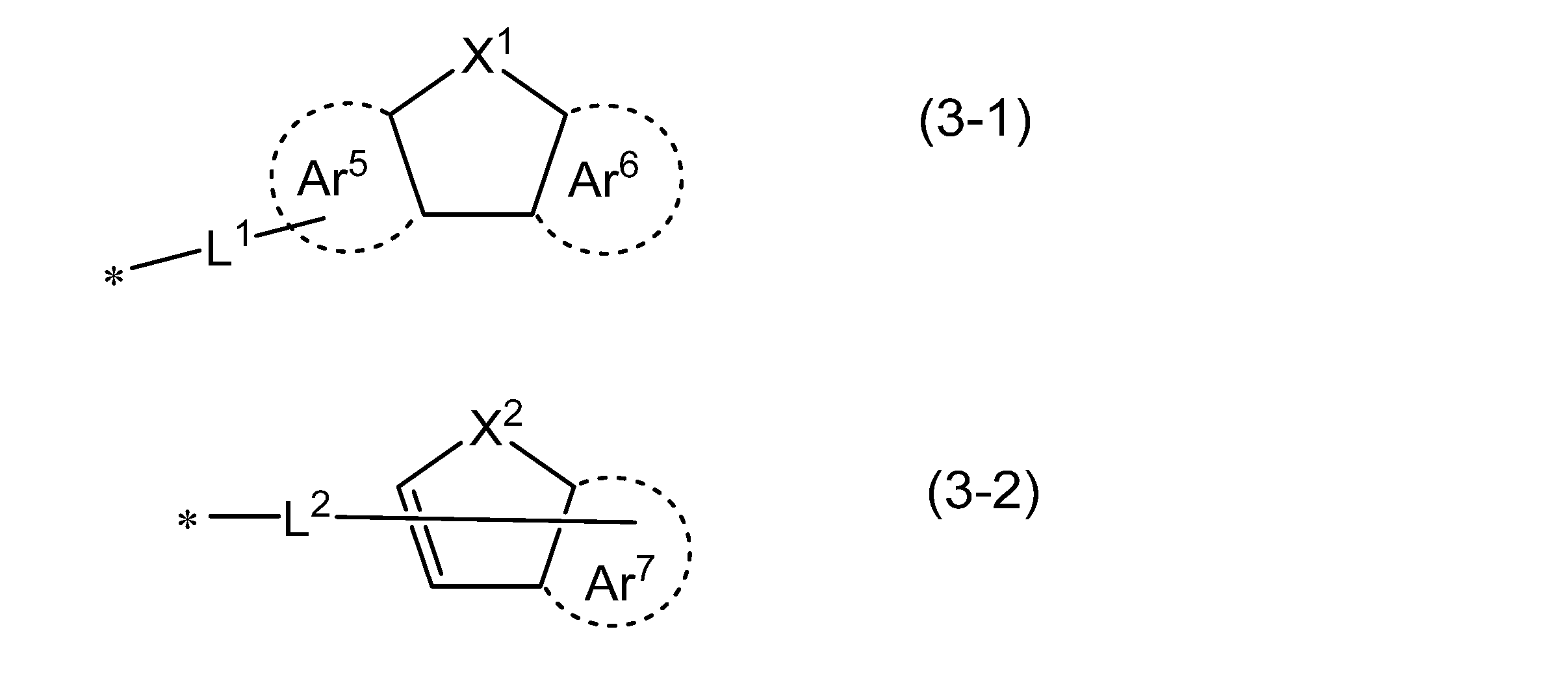
- R a is preferably a group represented by the following formula (3-1) or (3-2).
- X1 and X2 are each independently a group represented by the following formula (i), (ii), (iii) or (iv).
- Ar5 , Ar6 and Ar7 are each independently a substituted or unsubstituted aromatic ring having 6 to 20 ring members that forms a condensed ring structure together with two adjacent carbon atoms in formulas (3-1) and (3-2) above.
- L1 and L2 are each independently a divalent organic group having a single bond or an aromatic ring.
- R 11 and R 12 each independently represent a hydrogen atom or a monovalent organic group having 1 to 20 carbon atoms. At least one of R 11 and R 12 has an iodine atom.
- R 13 is a hydrogen atom or a monovalent organic group having 1 to 20 carbon atoms.
- R 14 is a monovalent organic group having 1 to 20 carbon atoms. At least one of R 13 and R 14 has an iodine atom.
- R 15 is a monovalent organic group having 1 to 20 carbon atoms and an iodine atom.
- R 16 is a monovalent organic group having 1 to 20 carbon atoms and containing a hydrogen atom or an iodine atom.
- Ar 5 , Ar 6 and Ar 7 are each independently a substituted or unsubstituted aromatic ring having 6 to 20 ring members which forms a condensed ring structure together with two adjacent carbon atoms in the above formulas (3-1) and (3-2).
- Ar 5 to Ar 7 an aromatic ring having 6 to 20 ring members among the aromatic rings having 5 to 40 ring members in Ar 1 in the above formula (1) can be suitably used.
- the substituent may be a hydroxy group, the above group ( ⁇ ), or any of the other substituents listed above.
- examples of the monovalent organic groups having 1 to 20 carbon atoms represented by R 11 , R 12 , R 13 , R 14 , R 15 and R 16 include groups corresponding to 1 to 20 carbon atoms among the monovalent organic groups having 1 to 40 carbon atoms represented by R 0 and R 1 in the above formula (1).
- At least one of R 11 and R 12 in the above formula (i), at least one of R 13 and R 14 in the above formula (ii), R 15 in the above formula (iii), and R 16 in the above formula (iv) each preferably have an aromatic ring having 5 to 40 ring members.
- an aromatic ring having 5 to 40 ring members in Ar 1 in the above formula (1) can be suitably adopted.
- it is preferable that at least one hydrogen atom of the aromatic ring is substituted with an iodine atom.
- the number of iodine atoms on the aromatic ring is preferably an integer of 1 to 4, more preferably an integer of 1 to 3, and even more preferably 1 or 2.
- the divalent organic group having an aromatic ring in L1 and L2 is preferably a substituted or unsubstituted group (hereinafter also referred to as "group ( ⁇ )") obtained by removing two hydrogen atoms from the aromatic ring having 5 to 40 ring members in Ar1 in the above formula (1).
- the divalent organic group having an aromatic ring represented by L1 and L2 may be a group obtained by combining the group ( ⁇ ) with a group obtained by removing one hydrogen atom from a monovalent organic group having 1 to 20 carbon atoms represented by the above R11 to R16 .
- the divalent organic group having an aromatic ring represented by L1 and L2 is preferably a substituted or unsubstituted arenediyl group having 6 to 12 ring members, a substituted or unsubstituted alkenediyl group having 2 to 10 carbon atoms, an alkynediyl group having 2 to 10 carbon atoms, or a combination thereof, more preferably a benzenediyl group, a naphthalenediyl group, an ethylenediyl group, an ethynediyl group, or a combination thereof, and even more preferably a benzenediyl group or a combination of a benzenediyl group and an ethynediyl group.
- L 1 and L 2 are preferably single bonds.
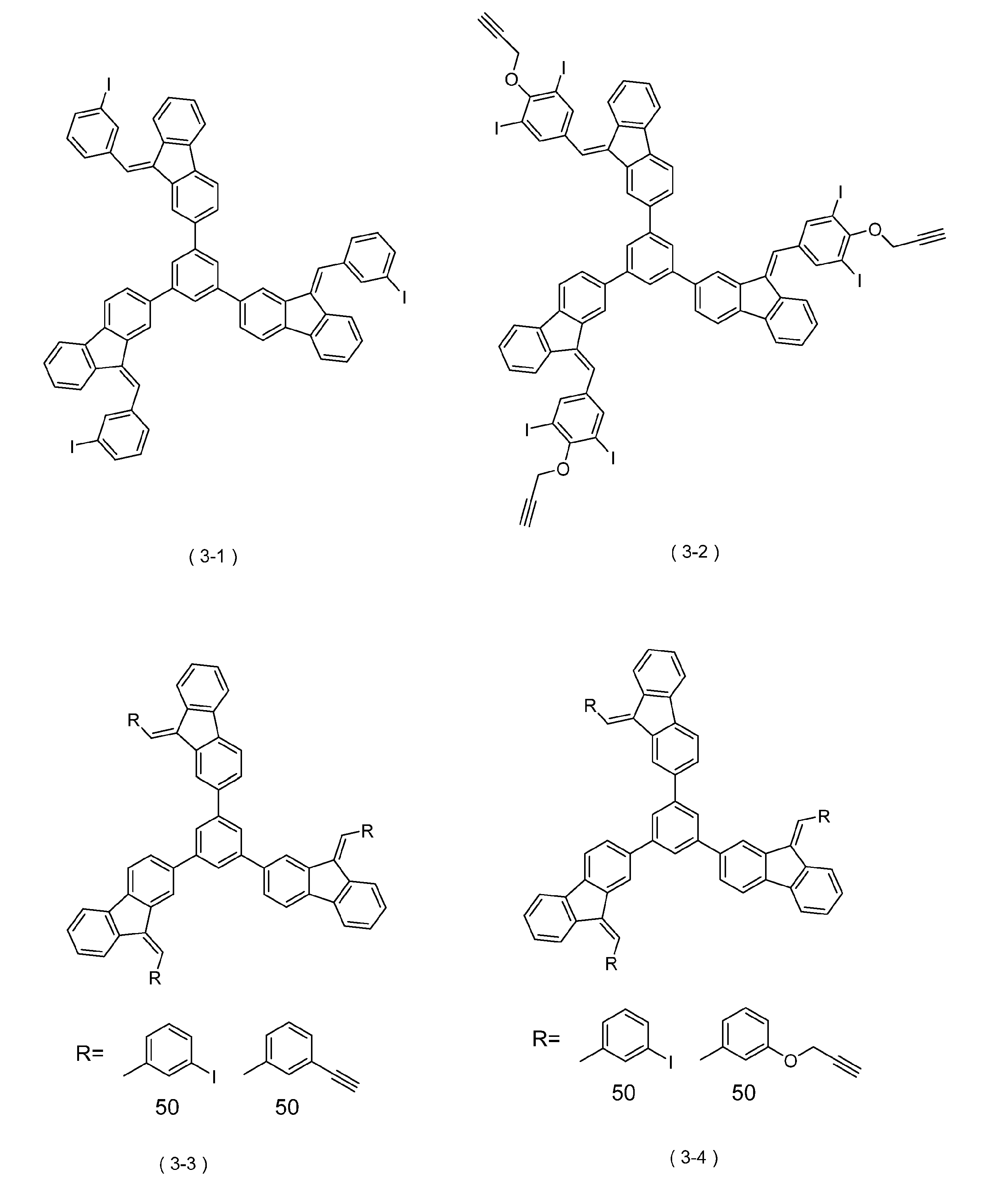
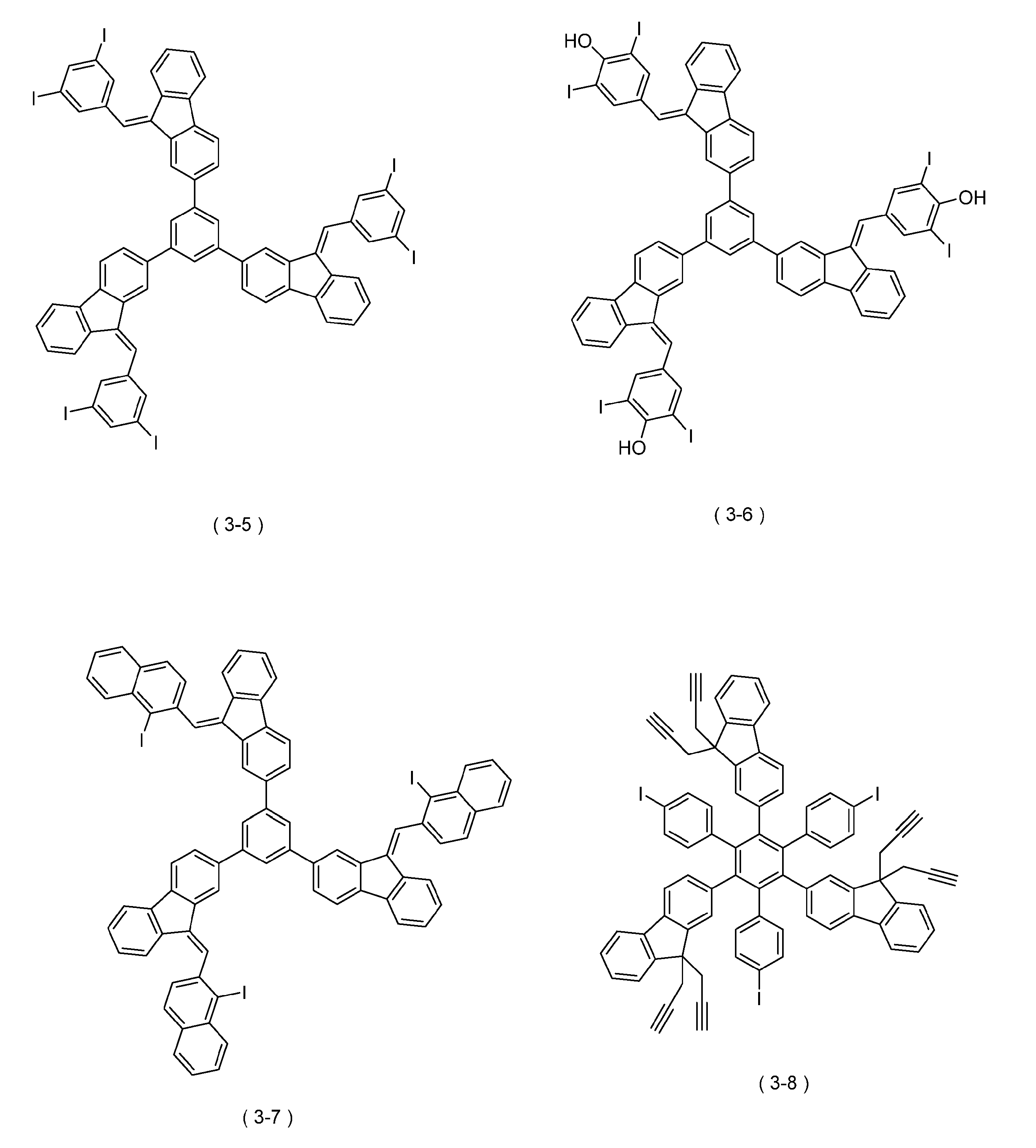
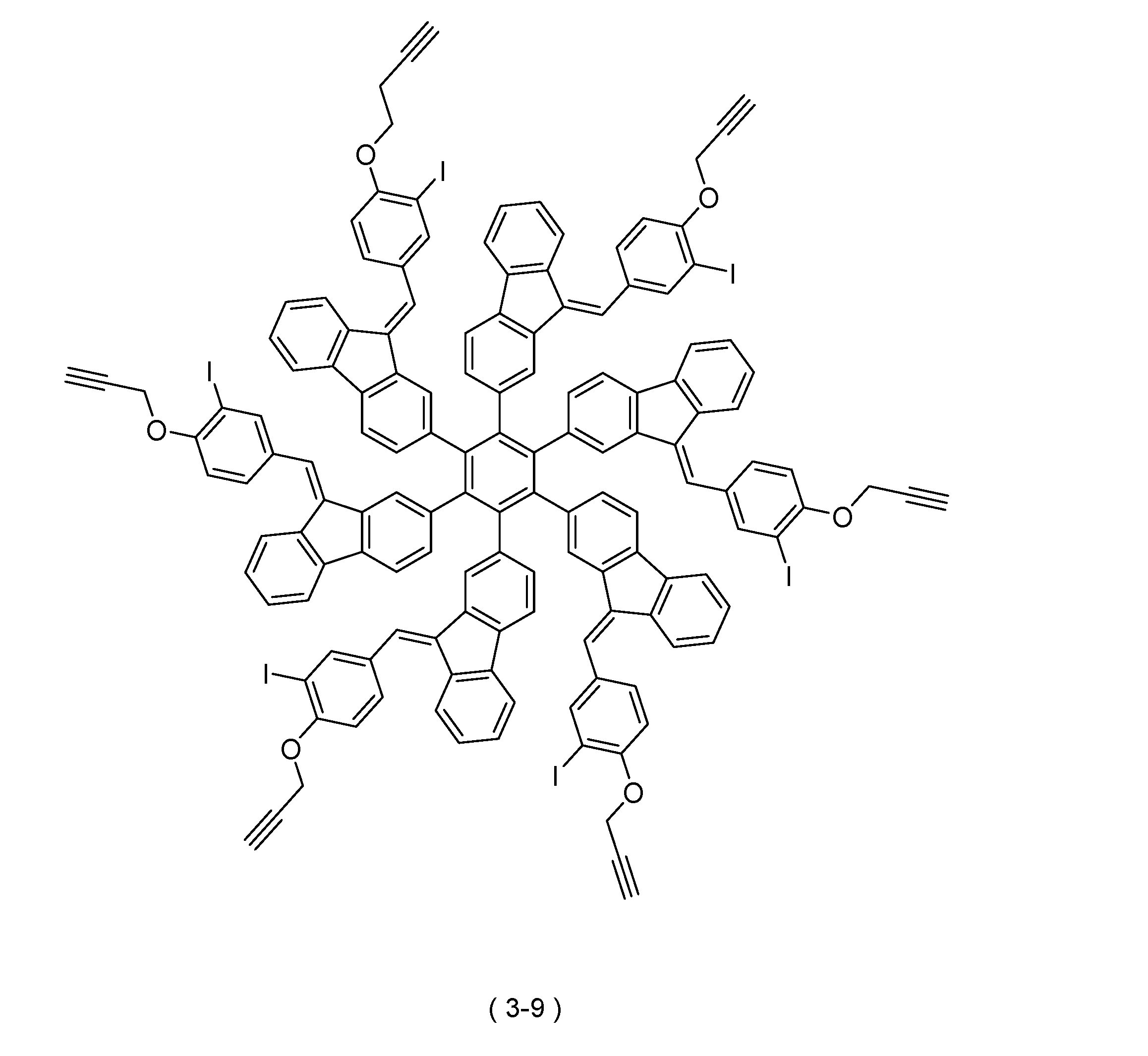
- aromatic ring-containing compound examples include compounds represented by the following formulas (3-1) to (3-9). In the formulas, the number attached to the structure representing R indicates the molar ratio in the aromatic ring-containing compound [A2].
- a typical method for synthesizing aromatic ring-containing compounds is to prepare a ketone or alkyne-substituted fluorene as a starting material, and then proceed with a cyclization reaction of the ketone or alkyne in the presence of a catalyst or the like.
- Other structures can also be synthesized by appropriately selecting the starting material, the structure of the ketone body, etc.
- the content of the compound [A] in the components other than the solvent in the composition for forming a resist underlayer film is 50% by mass or more.
- the lower limit of the content is preferably 60% by mass, more preferably 70% by mass, even more preferably 80% by mass, and particularly preferably 90% by mass.
- the upper limit of the content is preferably 100% by mass (i.e., the composition for forming a resist underlayer film contains only the compound [A] other than the solvent).
- the upper limit of the content is preferably 99% by mass, and more preferably 98% by mass.
- the lower limit of the content of the compound [A] in the composition is preferably 0.01% by mass, more preferably 0.05% by mass, even more preferably 0.1% by mass, and particularly preferably 0.5% by mass, based on the total mass of the compound [A] and the solvent [B].
- the upper limit of the content is preferably 30% by mass, more preferably 20% by mass, even more preferably 10% by mass, and particularly preferably 5% by mass, based on the total mass of the compound [A] and the solvent [B].
- the solvent (B) is not particularly limited as long as it can dissolve or disperse the compound (A) and any optional components contained as necessary.
- Solvents include, for example, hydrocarbon solvents, ester solvents, alcohol solvents, ketone solvents, ether solvents, nitrogen-containing solvents, etc. [B] Solvents can be used alone or in combination of two or more.
- hydrocarbon solvents examples include aliphatic hydrocarbon solvents such as n-pentane, n-hexane, and cyclohexane, and aromatic hydrocarbon solvents such as benzene, toluene, and xylene.
- ester solvents include carbonate solvents such as diethyl carbonate, acetate monoester solvents such as methyl acetate and ethyl acetate, lactone solvents such as gamma-butyrolactone, polyhydric alcohol partial ether carboxylate solvents such as diethylene glycol monomethyl ether acetate and propylene glycol monomethyl ether acetate, and lactate ester solvents such as methyl lactate and ethyl lactate.
- carbonate solvents such as diethyl carbonate
- acetate monoester solvents such as methyl acetate and ethyl acetate
- lactone solvents such as gamma-butyrolactone
- polyhydric alcohol partial ether carboxylate solvents such as diethylene glycol monomethyl ether acetate and propylene glycol monomethyl ether acetate
- lactate ester solvents such as methyl lactate and ethyl lactate.
- alcohol-based solvents examples include monoalcohol-based solvents such as methanol, ethanol, and n-propanol, and polyhydric alcohol-based solvents such as ethylene glycol and 1,2-propylene glycol.
- Ketone solvents include, for example, chain ketone solvents such as methyl ethyl ketone and methyl isobutyl ketone, and cyclic ketone solvents such as cyclohexanone.
- ether solvents include chain ether solvents such as n-butyl ether, polyhydric alcohol ether solvents such as cyclic ether solvents such as tetrahydrofuran, and polyhydric alcohol partial ether solvents such as diethylene glycol monomethyl ether.
- nitrogen-containing solvents examples include chain nitrogen-containing solvents such as N,N-dimethylacetamide, and cyclic nitrogen-containing solvents such as N-methylpyrrolidone.
- an ester solvent or a ketone solvent is preferable, a polyhydric alcohol partial ether carboxylate solvent or a cyclic ketone solvent is more preferable, and propylene glycol monomethyl ether acetate or cyclohexanone is even more preferable.
- the lower limit of the content of the solvent [B] in the composition is preferably 50% by mass, more preferably 60% by mass, even more preferably 70% by mass, and particularly preferably 80% by mass.
- the upper limit of the content is preferably 99.99% by mass, more preferably 99.98% by mass, even more preferably 99.9% by mass, and particularly preferably 99.5% by mass.
- the film-forming composition may contain optional components within the range that does not impair the effects of the present invention.
- optional components include an acid generator, a crosslinking agent, a surfactant, and a sensitizer.
- the composition may contain a polymer different from the polymer [A1] and an aromatic ring-containing compound different from the aromatic ring-containing compound [A2].
- the optional components may be used alone or in combination of two or more.
- composition for forming a resist underlayer film can be prepared by mixing the compound [A], the solvent [B], and, if necessary, any optional components in a predetermined ratio, and filtering the resulting mixture preferably through a membrane filter or the like having a pore size of 0.5 ⁇ m or less.
- the resist underlayer film forming composition is a composition for forming an underlayer film of a resist film to be exposed to extreme ultraviolet rays.
- the resist film forming composition include a positive or negative chemically amplified resist composition containing a radiation-sensitive acid generator, a positive resist composition containing an alkali-soluble resin and a quinone diazide-based photosensitizer, a negative resist composition containing an alkali-soluble resin and a crosslinking agent, and a metal-containing resist composition containing a metal such as tin, zirconium, or hafnium.
- the underlayer film formed by the composition contains iodine atoms derived from the compound [A], so that the efficiency of generating secondary electrons due to the absorption of extreme ultraviolet rays is high. As a result, a sufficient solubility difference occurs in the interface region on the underlayer film side of the organic resist film during exposure to extreme ultraviolet rays, and the insolubilization of the metal-containing resist film is promoted, thereby suppressing the tailing of the pattern at the bottom of the resist film and ensuring the rectangularity of the resist pattern.
- the lower limit of the content of the metal or metal compound in the components other than the solvent in the metal-containing resist composition is preferably 50% by mass, more preferably 70% by mass, even more preferably 80% by mass, and particularly preferably 85% by mass.
- the upper limit of the content is, for example, 100% by mass or 95% by mass.
- the underlayer film formed from this composition has an aromatic ring in the compound [A], which allows for the formation of a dense film through a crosslinking reaction, and the hydrophobic nature of the iodine atoms suppresses the above-mentioned intermixing, resulting in the formation of a desired pattern with suppressed defects.
- the method for manufacturing a semiconductor substrate includes a step of directly or indirectly applying a composition for forming a resist underlayer film to a substrate (hereinafter also referred to as a “coating step (I)”), a step of applying a composition for forming a resist film to the resist underlayer film formed by the above-mentioned coating step of the composition for forming a resist film (hereinafter also referred to as a “coating step (II)”), a step of exposing the resist film formed by the above-mentioned coating step of the composition for forming a resist film to extreme ultraviolet light (hereinafter also referred to as an "exposure step”), and a step of developing at least the exposed resist film (hereinafter also referred to as a "development step”).
- a resist underlayer film having excellent resist pattern rectangularity can be formed, and therefore a semiconductor substrate having a good pattern shape can be manufactured.
- the method for manufacturing the semiconductor substrate may further include, as necessary, a step of forming a silicon-containing film directly or indirectly on the substrate prior to the coating step (I) (hereinafter also referred to as the "silicon-containing film forming step").
- composition for forming a resist underlayer film used in the method for manufacturing a semiconductor substrate, and each step in the case where the method includes the optional silicon-containing film formation step.
- Silicon-containing film formation process In this step, which is carried out prior to the above coating step (I), a silicon-containing film is formed directly or indirectly on a substrate.
- the substrate examples include metal or semimetal substrates such as silicon substrates, aluminum substrates, nickel substrates, chromium substrates, molybdenum substrates, tungsten substrates, copper substrates, tantalum substrates, and titanium substrates, among which silicon substrates are preferred.
- the substrate may be a substrate on which a silicon nitride film, an alumina film, a silicon dioxide film, a tantalum nitride film, a titanium nitride film, or the like is formed.
- the silicon-containing film can be formed by coating a silicon-containing film-forming composition, chemical vapor deposition (CVD), atomic layer deposition (ALD), or the like.
- methods for forming a silicon-containing film by coating a silicon-containing film-forming composition include a method in which the silicon-containing film-forming composition is directly or indirectly coated on a substrate, and the coated film is then cured by exposure and/or heating.
- Examples of commercially available silicon-containing film-forming compositions include "NFC SOG01", “NFC SOG04", and "NFC SOG080” (all from JSR Corporation).
- Silicon oxide films, silicon nitride films, silicon oxynitride films, and amorphous silicon films can be formed by chemical vapor deposition (CVD) or atomic layer deposition (ALD).
- Radiation used for the above-mentioned exposure includes, for example, electromagnetic waves such as visible light, ultraviolet light, far ultraviolet light, X-rays, and gamma rays, as well as particle beams such as electron beams, molecular beams, and ion beams.
- the lower limit of the temperature when heating the coating film is preferably 90°C, more preferably 150°C, and even more preferably 200°C.
- the upper limit of the above temperature is preferably 550°C, more preferably 450°C, and even more preferably 300°C.
- the lower limit of the average thickness of the silicon-containing film is preferably 1 nm, more preferably 10 nm, and even more preferably 15 nm.
- the upper limit is preferably 20,000 nm, more preferably 1,000 nm, and even more preferably 100 nm.
- the average thickness of the silicon-containing film can be measured in the same manner as the average thickness of the resist underlayer film.
- Examples of the case where a silicon-containing film is indirectly formed on a substrate include a case where a silicon-containing film is formed on a low dielectric insulating film or an organic underlayer film formed on a substrate, a metal hard mask (such as TiO2 ), or a carbon film formed by a CVD method.
- the composition for forming resist underlayer film is coated on the silicon-containing film formed on the substrate.
- the coating method of the composition for forming resist underlayer film is not particularly limited, and can be carried out by suitable methods such as spin coating, casting coating, roll coating, etc.This forms a coating film, and the solvent [B] volatilizes, etc., to form a resist underlayer film.
- the silicon-containing film forming step can be omitted.
- Heating the coating film promotes the formation of the resist underlayer film. More specifically, heating the coating film promotes the evaporation of the solvent [B], etc.
- the coating film may be heated in an air atmosphere or in a nitrogen atmosphere.
- the lower limit of the heating temperature is preferably 100°C, more preferably 150°C, and even more preferably 200°C.
- the upper limit of the heating temperature is preferably 400°C, more preferably 350°C, and even more preferably 280°C.
- the lower limit of the heating time is preferably 15 seconds, and more preferably 30 seconds.
- the upper limit of the heating time is preferably 1,200 seconds, and more preferably 600 seconds.
- the resist underlayer film may be exposed to light.
- the resist underlayer film may be exposed to plasma.
- ions may be implanted into the resist underlayer film. Exposing the resist underlayer film to light improves the etching resistance of the resist underlayer film. Exposing the resist underlayer film to plasma improves the etching resistance of the resist underlayer film. Implanting ions into the resist underlayer film improves the etching resistance of the resist underlayer film.
- the radiation used to expose the resist underlayer film is appropriately selected from electromagnetic waves such as visible light, ultraviolet light, far ultraviolet light, X-rays, and gamma rays; and particle beams such as electron beams, molecular beams, and ion beams.
- the method of exposing the resist underlayer film to plasma includes, for example, a direct method in which the substrate is placed in a gas atmosphere and plasma discharge is performed.
- the conditions for plasma exposure are usually a gas flow rate of 50 cc/min to 100 cc/min, and a power supply of 100 W to 1,500 W.
- the lower limit of the plasma exposure time is preferably 10 seconds, more preferably 30 seconds, and even more preferably 1 minute.
- the upper limit of the above time is preferably 10 minutes, more preferably 5 minutes, and even more preferably 2 minutes.
- the plasma is generated in an atmosphere of a mixed gas of H2 gas and Ar gas, for example.
- a carbon-containing gas such as CF4 gas or CH4 gas may be introduced.
- CF4 gas NF3 gas, CHF3 gas , CO2 gas, CH2F2 gas, CH4 gas , and C4F8 gas may be introduced.
- Ion implantation of the resist underlayer film implants dopants into the resist underlayer film.
- the dopants may be selected from the group consisting of boron, carbon, nitrogen, phosphorus, arsenic, aluminum, and tungsten.
- the implant energy used to energize the dopants may range from about 0.5 keV to 60 keV depending on the type of dopant used and the desired depth of implantation.
- the lower limit of the average thickness of the resist underlayer film formed is preferably 0.5 nm, more preferably 1 nm, and even more preferably 2 nm.
- the upper limit of the average thickness is 15 nm, preferably 12 nm, more preferably 10 nm, even more preferably 8 nm, and particularly preferably 6 nm.
- the method for measuring the average thickness is as described in the Examples.
- a composition for forming a resist film is applied to the resist underlayer film formed in the above-mentioned step of applying the composition for forming a resist film.
- the method for applying the composition for forming a resist film is not particularly limited, and examples thereof include a rotational coating method.
- a resist film-forming composition is applied so that the resist film to be formed has a predetermined thickness, and then the composition is pre-baked (hereinafter also referred to as "PB") to volatilize the solvent in the applied film, thereby forming a resist film.
- PB pre-baked
- the PB temperature and PB time can be appropriately determined depending on the type of resist film forming composition used, etc.
- the lower limit of the PB temperature is preferably 30°C, and more preferably 50°C.
- the upper limit of the PB temperature is preferably 200°C, and more preferably 150°C.
- the lower limit of the PB time is preferably 10 seconds, and more preferably 30 seconds.
- the upper limit of the PB time is preferably 600 seconds, and more preferably 300 seconds.
- the resist film-forming composition used in this process is preferably a composition that is exposed to extreme ultraviolet rays, and examples of such compositions include positive or negative chemically amplified resist compositions that contain a radiation-sensitive acid generator, and metal-containing resist compositions that contain metals such as tin, zirconium, and hafnium.
- the resist film formed in the resist film forming composition application step is exposed to extreme ultraviolet (EUV) rays.
- EUV extreme ultraviolet
- the exposure conditions can be appropriately determined depending on the type of the resist film forming composition used, etc.
- PEB post-exposure baking
- the PEB temperature and PEB time can be appropriately determined depending on the type of resist film-forming composition used, etc.
- the lower limit of the PEB temperature is preferably 50°C, and more preferably 70°C.
- the upper limit of the PEB temperature is preferably 200°C, and more preferably 150°C.
- the lower limit of the PEB time is preferably 10 seconds, and more preferably 30 seconds.
- the upper limit of the PEB time is preferably 600 seconds, and more preferably 300 seconds.
- the exposed resist film is developed. At this time, a part of the resist underlayer film may be further developed.
- the developer used in this development include an alkaline aqueous solution (alkaline developer), an organic solvent-containing liquid (organic solvent developer), and the like.
- the basic liquid for alkaline development is not particularly limited, and any known basic liquid can be used.
- Examples of basic liquids for alkaline development include aqueous alkaline solutions in which at least one of the following alkaline compounds is dissolved: sodium hydroxide, potassium hydroxide, sodium carbonate, sodium silicate, sodium metasilicate, aqueous ammonia, ethylamine, n-propylamine, diethylamine, di-n-propylamine, triethylamine, methyldiethylamine, ethyldimethylamine, triethanolamine, tetramethylammonium hydroxide (TMAH), pyrrole, piperidine, choline, 1,8-diazabicyclo-[5.4.0]-7-undecene, 1,5-diazabicyclo-[4.3.0]-5-nonene, etc.
- TMAH tetramethylammonium hydroxide
- TMAH tetramethylammonium hydrox
- examples of the organic solvent developer include those exemplified as the solvent [B] above.
- organic solvent developer ester-based solvents, ether-based solvents, alcohol-based solvents, ketone-based solvents and/or hydrocarbon-based solvents are preferred, ketone-based solvents are more preferred, and 2-heptanone is particularly preferred.
- washing and/or drying may be performed after the development.
- etching is performed using the resist pattern (and resist underlayer film pattern) as a mask.
- the number of times of etching may be one or more, that is, etching may be performed sequentially using the pattern obtained by etching as a mask. From the viewpoint of obtaining a pattern with a better shape, multiple times are preferable.
- etching is performed sequentially in the order of the silicon-containing film and the substrate.
- the etching method include dry etching and wet etching. From the viewpoint of obtaining a better shape of the pattern of the substrate, dry etching is preferable. For this dry etching, for example, gas plasma such as oxygen plasma is used.
- Dry etching can be performed, for example, using a known dry etching device.
- the etching gas used in dry etching can be appropriately selected according to the mask pattern, the elemental composition of the film to be etched, etc., and can include, for example, fluorine-based gases such as CHF3, CF4, C2F6 , C3F8 , SF6 , etc.
- chlorine-based gases such as Cl2 , BCl3
- oxygen-based gases such as O2 , O3 , H2O , H2 , CO, CO2 , CH4 , C2H2 , C2H4 , C2H6 , C3H4 , C3H6 , C3H8 , HF, HI, HBr, HCl, NO, NH3 , BCl3, etc.
- reducing gases inert gases such as He, N2 , Ar, etc.
- gases can also be used in mixture.
- a fluorine-based gas is usually used.
- the silicon-containing film can be removed by carrying out a removal process.
- Mw Weight average molecular weight
- the average thickness of the film was determined by measuring the film thickness at any nine positions at 5 cm intervals including the center of the resist underlayer film formed on the silicon wafer using a spectroscopic ellipsometer (J.A. WOOLLAM's "M2000D") and calculating the average value of the film thicknesses.
- the introduction rate of the propargyl group was determined by 13 C-NMR analysis using a measurement sample prepared by dissolving compound [A] in DMSO- d6 solvent containing 5% chromium acetylacetate, using a JEOL Ltd. " JNM -ECX400P" analyzer.
- the reaction solution was transferred to a separatory funnel, and 100 g of methyl isobutyl ketone and 200 g of water were added to wash the organic phase. After separating the aqueous phase, the obtained organic phase was washed several times with water. Then, the mixture was concentrated with an evaporator, and the residue was dropped into 100 g of methanol to obtain a precipitate. The precipitate was collected by suction filtration and washed several times with 50 g of methanol. Then, the mixture was dried in a vacuum dryer at 60 ° C. for 12 hours to obtain a polymer (A-1) having a repeating unit represented by the following formula (A-1). The Mw of the polymer (A-1) was 2,390.
- the reaction solution was transferred to a separatory funnel, and 100 g of methyl isobutyl ketone and 200 g of a 5% aqueous oxalic acid solution were added to separate the organic phase.
- the obtained organic phase was concentrated with an evaporator and dropped into 150 g of methanol to obtain a precipitate.
- the precipitate was collected by suction filtration and washed several times with 50 g of methanol.
- the mixture was dried in a vacuum dryer at 60° C. for 12 hours to obtain a polymer (A-13) having a repeating unit represented by the following formula (A-13).
- the Mw of the polymer (A-13) was 3,115, and the introduction rate of the propargyl group in the polymer (A-13) was 83% based on the total hydroxy groups.
- the obtained organic phase was concentrated with an evaporator and dropped into 300 g of methanol to obtain a precipitate.
- the precipitate was collected by suction filtration and washed several times with 50.0 g of methanol. Then, it was dried in a vacuum dryer at 60°C for 12 hours.
- 50.0 g of methyl isobutyl ketone, 20.0 g of methanol, and 7.3 g of tetramethylammonium hydroxide (25% aqueous solution) were added to 10.0 g of the obtained compound, and the mixture was stirred at room temperature for several minutes.
- 2.4 g of propargyl bromide was added, and the mixture was heated from room temperature to 40° C.
- the reaction solution was transferred to a separatory funnel, and 200 g of methyl isobutyl ketone and 200 g of a 5% aqueous oxalic acid solution were added to separate the organic phase.
- the obtained organic phase was concentrated with an evaporator and dropped into 300 g of methanol to obtain a precipitate.
- the precipitate was collected by suction filtration and washed several times with 50 g of methanol. Then, the mixture was dried in a vacuum dryer at 60° C. for 12 hours to obtain a compound (A-26) represented by the following formula (A-26).
- the introduction rate of the propargyl group in the compound (A-26) was 82% with respect to the total hydroxyl groups.
- the organic phase was washed several times with water, and then the resulting organic phase was concentrated using an evaporator and dropped into 100 g of hexane to obtain a precipitate.
- the precipitate was collected by suction filtration and washed several times with 50.0 g of hexane. Thereafter, the precipitate was dried in a vacuum dryer at 60° C. for 12 hours to obtain a polymer (X-1) represented by the following formula (X-1).
- the Mw of the polymer (X-1) was 4,420.
- E-1 A polymer having a repeating unit represented by the following formula (E-1) (Mw: 1500)
- E-2 A polymer having a repeating unit represented by the following formula (E-2) (Mw: 1800)
- E-3 A compound represented by the following formula (E-3):
- Example 1-1 2 parts by mass of (A-1) as the compound [A], 0.05 parts by mass of (C-1) as the acid generator [C], and 0.05 parts by mass of (D-1) as the crosslinking agent [D] were dissolved in 97.9 parts by mass of (B-1) as the solvent [B].
- the resulting solution was filtered through a polytetrafluoroethylene (PTFE) membrane filter having a pore size of 0.45 ⁇ m to prepare a composition (J-1).
- PTFE polytetrafluoroethylene
- Example 1-1 Compositions (J-2) to (J-30) and (CJ-1) were prepared in the same manner as in Example 1, except that the types and amounts of each component were used as shown in Table 1 below.
- Table 1 the "-" in the columns “[C] Acid generator” and “[D] Crosslinker” indicates that the corresponding component was not used.
- PTFE polytetrafluoroethylene
- an organic underlayer film forming material (“HM8006” by JSR Corporation) was applied by a spin coating method using a spin coater ("CLEAN TRACK ACT12" by Tokyo Electron Co., Ltd.), and then heated at 250 ° C. for 60 seconds to form an organic underlayer film with an average thickness of 100 nm.
- a silicon-containing film forming composition (“NFC SOG080” by JSR Corporation) was applied, heated at 220 ° C. for 60 seconds, and then cooled at 23 ° C. for 30 seconds to form a silicon-containing film with an average thickness of 20 nm.
- the resist underlayer film forming composition prepared above was applied, heated at 250 ° C. for 60 seconds, and then cooled at 23 ° C. for 30 seconds to form a resist underlayer film with an average thickness of 5 nm.
- a resist composition (R-1) was applied onto the resist underlayer film formed above, heated at 130° C. for 60 seconds, and then cooled at 23° C. for 30 seconds to form a resist film having an average thickness of 50 nm.
- the resist film was irradiated with extreme ultraviolet rays using an EUV scanner (ASML's "TWINSCAN NXE:3300B" (NA 0.3, sigma 0.9, quadrupole illumination, 1:1 line and space mask with a line width of 16 nm on the wafer).
- EUV scanner ASML's "TWINSCAN NXE:3300B” (NA 0.3, sigma 0.9, quadrupole illumination, 1:1 line and space mask with a line width of 16 nm on the wafer).
- the substrate was heated at 110°C for 60 seconds, and then cooled at 23°C for 60 seconds. Thereafter, a 2.38 mass% aqueous solution of tetramethylammonium hydroxide (20°C to 25°C) was used for development by the paddle method, followed by washing with water and drying to obtain an evaluation substrate on which a resist pattern was formed.
- a scanning electron microscope (Hitachi High-Tech's "SU8220") was used to measure and observe the resist pattern of the evaluation substrate.
- the rectangularity of the resist pattern was evaluated as "A” (good) when the cross-sectional shape of the pattern was rectangular, and as "B” (bad) when the cross-section of the pattern had a skirt.
- Compound (S-1) was an oxide hydroxide product of a hydrolysis product of isopropyltin trichloride (having a structural unit of i-PrSnO (3/2-x/2) (OH) x (0 ⁇ x ⁇ 3)).
- resist composition (R-2) 2 parts by weight of the compound (S-1) synthesized above was mixed with 98 parts by weight of propylene glycol monoethyl ether, and the resulting mixture was passed through an activated 4 ⁇ molecular sieve to remove residual water, and then filtered through a polytetrafluoroethylene (PTFE) membrane filter with a pore size of 0.2 ⁇ m to prepare resist composition (R-2).
- PTFE polytetrafluoroethylene
- resist composition (R-2) was applied by a spin coating method using the spin coater, and after a predetermined time had elapsed, the resist film was heated at 90°C for 60 seconds, and then cooled at 23°C for 30 seconds to form a resist film having an average thickness of 35 nm.
- the resist film was exposed to light using an EUV scanner (ASML's "TWINSCAN NXE:3300B" (NA 0.3, sigma 0.9, quadrupole illumination, 1:1 line and space mask with a line width of 25 nm on the wafer). After exposure, the substrate was heated at 110°C for 60 seconds and then cooled at 23°C for 60 seconds.
- the substrate was developed by the paddle method using 2-heptanone (20 to 25°C) and then dried to obtain an evaluation substrate on which a resist pattern was formed.
- a scanning electron microscope (Hitachi High-Tech's "SU8220") was used to measure and observe the resist pattern of the evaluation substrate.
- the rectangularity of the resist pattern was evaluated as "A” (good) when the cross-sectional shape of the pattern was rectangular, and as "B” (bad) when the cross-sectional shape of the pattern had a footing.
- a scanning electron microscope (Hitachi High-Technologies Corporation's "SU8220") was used to observe the pattern of the evaluation substrate.
- defect suppression after etching was evaluated as "A" (good) when there was no residue (defect) in the part where the resist underlayer film was selectively removed in the cross section of the resist underlayer film pattern, and as “B” (bad) when there was residue (defect).
- the resist underlayer film formed from the resist underlayer film forming composition of the Example had superior resist pattern rectangularity and post-etching defect suppression properties compared to the resist underlayer film formed from the resist underlayer film forming composition of the Comparative Example.
- the resist underlayer film forming composition of the present invention can form a film with excellent resist pattern rectangularity.
- the semiconductor substrate manufacturing method of the present invention uses a resist underlayer film forming composition capable of forming a resist underlayer film with excellent resist pattern rectangularity, so that semiconductor substrates can be manufactured efficiently. Therefore, these can be suitably used in the manufacture of semiconductor devices, which are expected to become even more miniaturized in the future.
Landscapes
- Physics & Mathematics (AREA)
- General Physics & Mathematics (AREA)
- Engineering & Computer Science (AREA)
- Architecture (AREA)
- Structural Engineering (AREA)
- Chemical & Material Sciences (AREA)
- Organic Chemistry (AREA)
- Metallurgy (AREA)
- Spectroscopy & Molecular Physics (AREA)
- Materials For Photolithography (AREA)
- Exposure Of Semiconductors, Excluding Electron Or Ion Beam Exposure (AREA)
- Compositions Of Macromolecular Compounds (AREA)
- Optics & Photonics (AREA)
Abstract
Description
極端紫外線での露光に供されるレジスト膜の下層膜形成用組成物であって、
ヨウ素原子を有する化合物(以下、「[A]化合物」ともいう。)と、
溶媒(以下、「[B]溶媒」ともいう。)と
を含み、
上記ヨウ素原子を有する化合物が、下記式(1)で表される繰り返し単位を有する重合体(以下、「[A1]重合体」ともいう。)、ヨウ素原子を有する分子量が750以上3000以下の芳香環含有化合物(以下、「[A2]芳香環含有化合物」ともいう。)又はこれらの組み合わせであり、
上記下層膜形成用組成物における溶媒以外の成分に占める上記ヨウ素原子を有する化合物の含有割合が50質量%以上である、レジスト下層膜形成用組成物に関する。

基板に直接又は間接にレジスト下層膜形成用組成物を塗工する工程と、
上記レジスト下層膜形成用組成物塗工工程により形成されたレジスト下層膜にレジスト膜形成用組成物を塗工する工程と、
上記レジスト膜形成用組成物塗工工程により形成されたレジスト膜を極端紫外線により露光する工程と、
少なくとも上記露光されたレジスト膜を現像する工程と
を備え、
上記レジスト下層膜形成用組成物が、
ヨウ素原子を有する化合物と、
溶媒と
を含み、
上記ヨウ素原子を有する化合物が、下記式(1)で表される繰り返し単位を有する重合体、ヨウ素原子を有する分子量が750以上3000以下の芳香環含有化合物又はこれらの組み合わせであり、
上記下層膜形成用組成物における溶媒以外の成分に占める上記ヨウ素原子を有する化合物の含有割合が50質量%以上である、半導体基板の製造方法に関する。
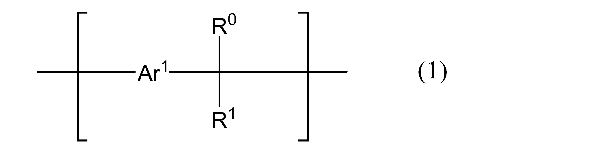
当該レジスト下層膜形成用組成物(以下、単に「組成物」ともいう。)は、極端紫外線での露光に供されるレジスト膜の下層膜形成用組成物として用いられ、[A]化合物と[B]溶媒とを含有する。当該組成物は、本発明の効果を損なわない範囲において、任意成分を含有していてもよい。
[A]化合物は、ヨウ素原子を有する化合物であり、[A1]重合体、[A2]芳香環含有化合物(ただし、[A1]重合体に該当する化合物を除く。)又はこれらの組み合わせである。[A1]重合体及び[A2]芳香環含有化合物はそれぞれ1種単独で又は2種以上を組み合わせて用いることができる。
[A]化合物としての[A1]重合体は、下記式(1)で表される繰り返し単位を有する重合体である。[A1]重合体は、下記式(1)で表される繰り返し単位を2種以上有していてもよい。


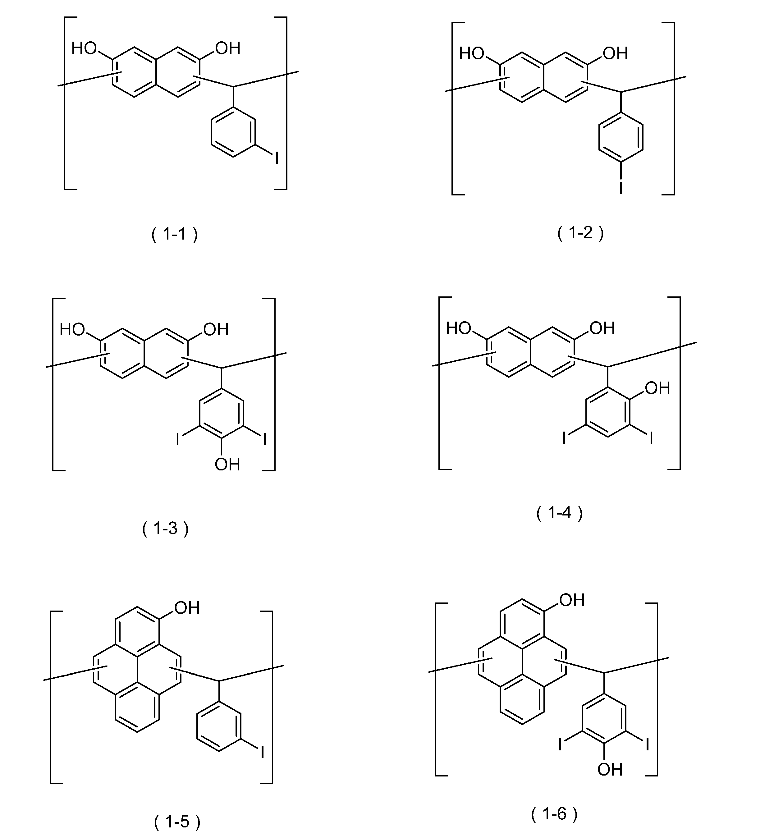


[A1]重合体は、代表的に、上記式(1)のAr1を与えるフェノール性水酸基を有する前駆体としての芳香環化合物と、上記式(1)のR0及びR1を与える前駆体としてのアルデヒド誘導体との酸付加縮合により製造することができる。さらに、上記式(2-1)又は(2-2)で表される基(α)に対応するハロゲン化炭化水素へのフェノール性水酸基による求核置換反応により、置換基として基(α)を導入した[A1]重合体を製造することができる。酸触媒としては特に限定されず、公知の無機酸及び有機酸を用いることができる。反応後、分離、精製、乾燥等を経て[A1]重合体を得ることができる。反応溶媒としては、後述の[B]溶媒を好適に採用することができる。
[A2]芳香環含有化合物は、ヨウ素原子を有し、かつ分子量が750以上3000以下の化合物である限り特に限定されない(ただし、[A1]重合体に該当する化合物を除く。)。[A2]芳香環含有化合物の分子量の下限としては、750が好ましく、950がより好ましく、1050がさらに好ましい。上記分子量の上限としては、3000が好ましく、2500がより好ましく、2000がさらに好ましい。

Wは、置換又は非置換の環員数5~60の芳香環を含むq価の基である。
Raは、環員数5~40の芳香環を含む1価の基である。
qは1~10の整数である。qが2以上である場合、複数のRaは、互いに同一又は異なる。
W及び1又は複数のRaのうちの少なくとも1つはヨウ素原子を有する。)
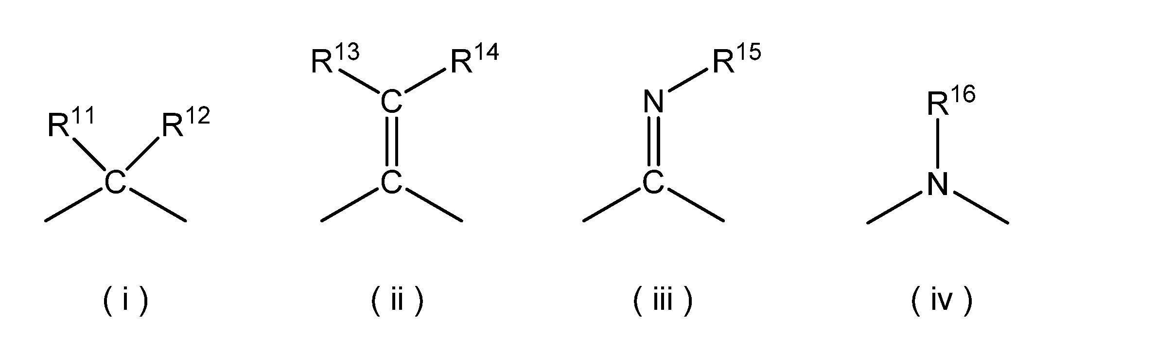
式(ii)中、R13は、水素原子又は炭素数1~20の1価の有機基である。R14は、炭素数1~20の1価の有機基である。R13及びR14のうちの少なくとも1つがヨウ素原子有する。
式(iii)中、R15は、ヨウ素原子を有する炭素数1~20の1価の有機基である。
式(iv)中、R16は、水素原子又はヨウ素原子を有する炭素数1~20の1価の有機基である。)
[B]溶媒は、[A]化合物及び必要に応じて含有する任意成分を溶解又は分散することができれば特に限定されない。
当該膜形成用組成物は、本発明の効果を損なわない範囲において任意成分を含有していてもよい。任意成分としては、例えば酸発生剤、架橋剤、界面活性剤、増感剤等が挙げられる。その他の成分として、[A1]重合体と異なる重合体、[A2]芳香環含有化合物と異なる芳香環含有化合物を含有してもよい。任意成分は、1種単独で又は2種以上を組み合わせて用いることができる。
当該レジスト下層膜形成用組成物は、[A]化合物、[B]溶媒、及び必要に応じて任意成分を所定の割合で混合し、好ましくは得られた混合物を孔径0.5μm以下のメンブランフィルター等でろ過することにより調製できる。
当該レジスト下層膜形成用組成物は、上述のように、極端紫外線での露光に供されるレジスト膜の下層膜形成用組成物である。レジスト膜形成用組成物としては、例えば、感放射線性酸発生剤を含有するポジ型又はネガ型の化学増幅型レジスト組成物、アルカリ可溶性樹脂とキノンジアジド系感光剤とを含有するポジ型レジスト組成物、アルカリ可溶性樹脂と架橋剤とを含有するネガ型レジスト組成物、スズ、ジルコニウム、ハフニウムなどの金属を含有する金属含有レジスト組成物等をあげることができる。当該組成物により形成される下層膜は[A]化合物に由来するヨウ素原子を含有するので、極端紫外線の吸収による二次電子の発生効率が高くなっている。その結果、極端紫外線での露光の際に有機レジスト膜における下層膜側の界面領域において十分な溶解性の差が生じたり、金属含有レジスト膜の不溶化を促進したりすることで、レジスト膜底部でのパターンの裾引きを抑制してレジストパターンの矩形性を確保することができる。金属含有レジスト組成物における溶媒以外の成分に占める金属又は金属化合物の含有割合の下限としては、50質量%が好ましく、70質量%がより好ましく、80質量%がさらに好ましく、85質量%が特に好ましい。上記含有割合の上限としては、例えば100質量%、95質量%が挙げられる。
当該半導体基板の製造方法は、基板に直接又は間接にレジスト下層膜形成用組成物を塗工する工程(以下、「塗工工程(I)」ともいう。)と、上記レジスト下層膜形成用組成物塗工工程により形成されたレジスト下層膜にレジスト膜形成用組成物を塗工する工程(以下、「塗工工程(II)」ともいう。)と、上記レジスト膜形成用組成物塗工工程により形成されたレジスト膜を極端紫外線により露光する工程(以下、「露光工程」ともいう。)と、少なくとも上記露光されたレジスト膜を現像する工程(以下、「現像工程」ともいう。)とを備える。
上記塗工工程(I)より前に行う本工程では、基板に直接又は間接にケイ素含有膜を形成する。
本工程では、上記基板に形成された上述のケイ素含有膜上にレジスト下層膜形成用組成物を塗工する。レジスト下層膜形成用組成物の塗工方法としては特に限定されず、例えば回転塗工、流延塗工、ロール塗工などの適宜の方法で実施することができる。これにより塗工膜が形成され、[B]溶媒の揮発などが起こることによりレジスト下層膜が形成される。
本工程では、上記レジスト下層膜形成用組成物塗工工程により形成されたレジスト下層膜にレジスト膜形成用組成物を塗工する。レジスト膜形成用組成物の塗工方法としては特に制限されず、例えば回転塗工法等が挙げられる。
本工程では、上記レジスト膜形成用組成物塗工工程により形成されたレジスト膜を極端紫外線(EUV)により露光する。露光条件は用いるレジスト膜形成用組成物の種類等に応じて適宜決定することができる。
本工程では、上記露光されたレジスト膜を現像する。この際、さらにレジスト下層膜の一部を現像してもよい。この現像に用いる現像液としては、アルカリ水溶液(アルカリ現像液)、有機溶媒含有液(有機溶媒現像液)等が挙げられる。
本工程では、上記レジストパターン(及びレジスト下層膜パターン)をマスクとしたエッチングを行う。エッチングの回数としては1回でも、複数回、すなわちエッチングにより得られるパターンをマスクとして順次エッチングを行ってもよい。より良好な形状のパターンを得る観点からは、複数回が好ましい。複数回のエッチングを行う場合、例えばケイ素含有膜及び基板の順に順次エッチングを行う。エッチングの方法としては、ドライエッチング、ウエットエッチング等が挙げられる。基板のパターンの形状をより良好なものとする観点からは、ドライエッチングが好ましい。このドライエッチングには、例えば酸素プラズマ等のガスプラズマなどが用いられる。上記エッチングにより、所定のパターンを有する半導体基板が得られる。
重合体のMwは、東ソー(株)のGPCカラム(「G2000HXL」2本、「G3000HXL」1本、及び「G4000HXL」1本)を用い、流量:1.0mL/分、溶出溶媒:テトラヒドロフラン、カラム温度:40℃の分析条件で、単分散ポリスチレンを標準とするゲルパーミエーションクロマトグラフィー(検出器:示差屈折計)により測定した。
膜の平均厚みは、分光エリプソメータ(J.A.WOOLLAM社の「M2000D」)を用いて、シリコンウェハ上に形成されたレジスト下層膜の中心を含む5cm間隔の任意の9点の位置で膜厚を測定し、それらの膜厚の平均値を算出した値として求めた。
プロパルギル基の導入率は、アセチル酢酸クロムを5%添加したDMSO-d6溶媒に[A]化合物を溶解させたものを測定試料として、日本電子株式会社製「JNM-ECX400P」を用い、13C-NMR分析により求めた。
反応容器に、窒素雰囲気下、2,7-ジヒドロキシナフタレン10.0g、3-ヨードベンズアルデヒド14.5gおよび1-ブタノール65.0gを仕込み、攪拌させて化合物を溶解させた。p-トルエンスルホン酸1水和物5.9gの1-ブタノール溶液9.0gを反応容器に添加した後、110℃に加熱して12時間反応させた。反応終了後、反応溶液を分液ロートに移し、メチルイソブチルケトン100gと水200gを加えて有機相を洗浄した。水相を分離した後、得られた有機相を数回、水で洗浄した。その後、エバポレーターで濃縮し、残渣をメタノール100g中に滴下させて沈殿物を得た。沈殿物を吸引濾過により回収し、メタノール50gで数回洗浄した。その後、真空乾燥機内にて60℃で12時間乾燥することにより、下記式(A-1)で表される繰り返し単位を有する重合体(A-1)を得た。重合体(A-1)のMwは2390であった。

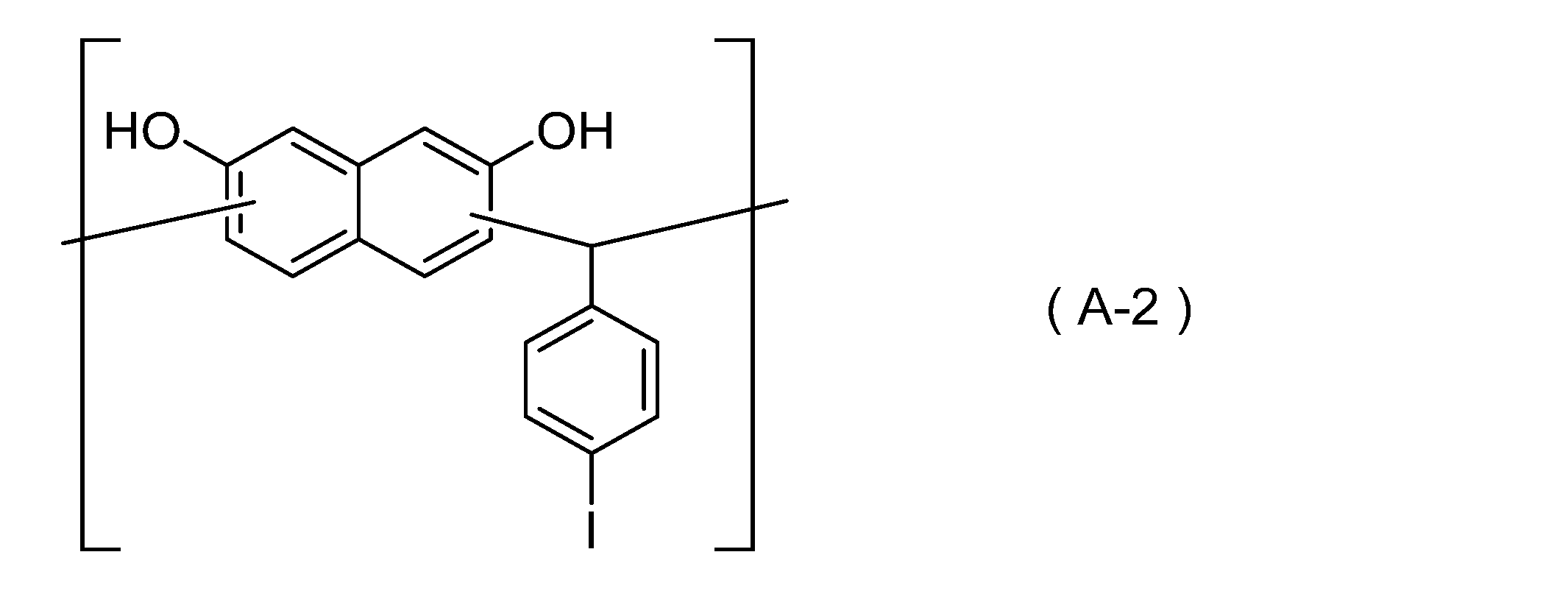
3-ヨードベンズアルデヒド14.5gの代わりに、4-ヨードベンズアルデヒド14.5gに変えたこと以外は[合成例1]と同様の条件で反応させることにより、下記式(A-2)で表される繰り返し単位を有する重合体(A-2)を得た。重合体(A-2)のMwは2500であった。
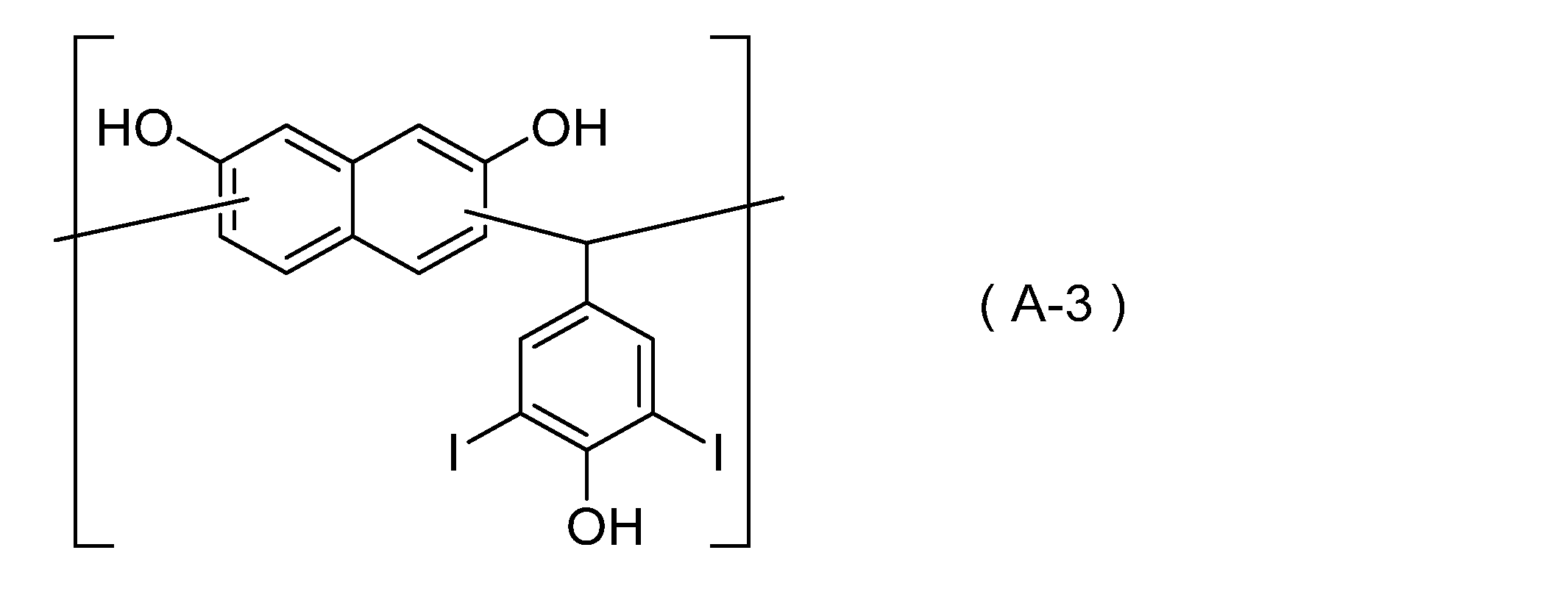
3-ヨードベンズアルデヒド14.5gの代わりに、3,5-ジヨード-4-ヒドロキシベンズアルデヒド23.3gに変えたこと以外は[合成例1]と同様の条件で反応させることにより、下記式(A-3)で表される繰り返し単位を有する重合体(A-3)を得た。重合体(A-3)のMwは2900であった。
3-ヨードベンズアルデヒド23.3gの代わりに、3,5-ジヨード-2-ヒドロキシベンズアルデヒド23.3gに変えたこと以外は[合成例1]と同様の条件で反応させることにより、下記式(A-4)で表される繰り返し単位を有する重合体(A-4)を得た。重合体(A-4)のMwは3100であった。

2,7-ジヒドロキシナフタレン10.0gの代わりに、1-ヒドロキシピレン13.7gに変えたこと以外は[合成例1]と同様の条件で反応させることにより、下記式(A-5)で表される繰り返し単位を有する重合体(A-5)を得た。重合体(A-5)のMwは3400であった。

2,7-ジヒドロキシナフタレン10.0gの代わりに、1-ヒドロキシピレン13.7gに変えたこと以外は[合成例3]と同様の条件で反応させることにより、下記式(A-6)で表される繰り返し単位を有する重合体(A-6)を得た。重合体(A-6)のMwは3200であった。

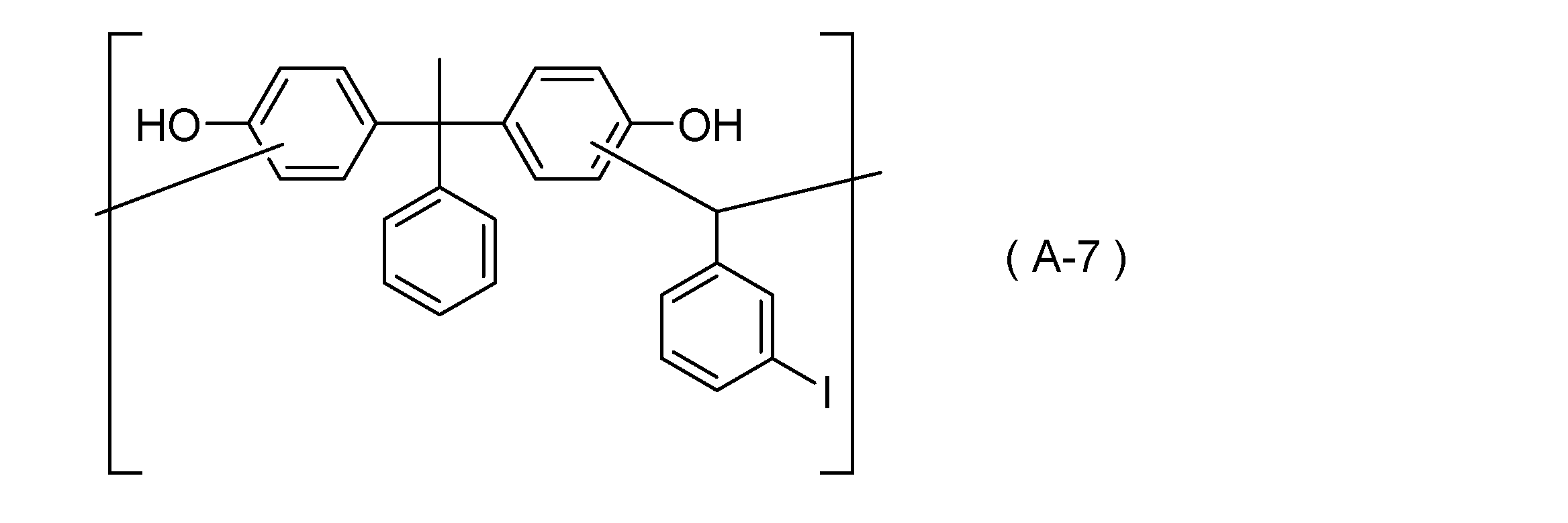
2,7-ジヒドロキシナフタレン10.0gの代わりに、1,1-ビス(4-ヒドロキシフェニル)-1-フェニルエタン18.1gに変えたこと以外は[合成例1]と同様の条件で反応させることにより、下記式(A-7)で表される繰り返し単位を有する重合体(A-7)を得た。重合体(A-7)のMwは3000であった。
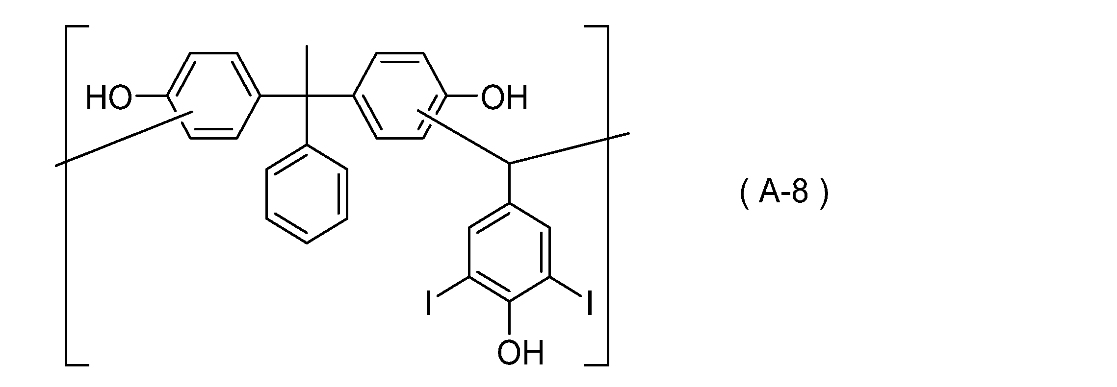
2,7-ジヒドロキシナフタレン10.0gの代わりに、1,1-ビス(4-ヒドロキシフェニル)-1-フェニルエタン18.1gに変えたこと以外は[合成例3]と同様の条件で反応させることにより、下記式(A-8)で表される繰り返し単位を有する重合体(A-8)を得た。重合体(A-8)のMwは2310であった。
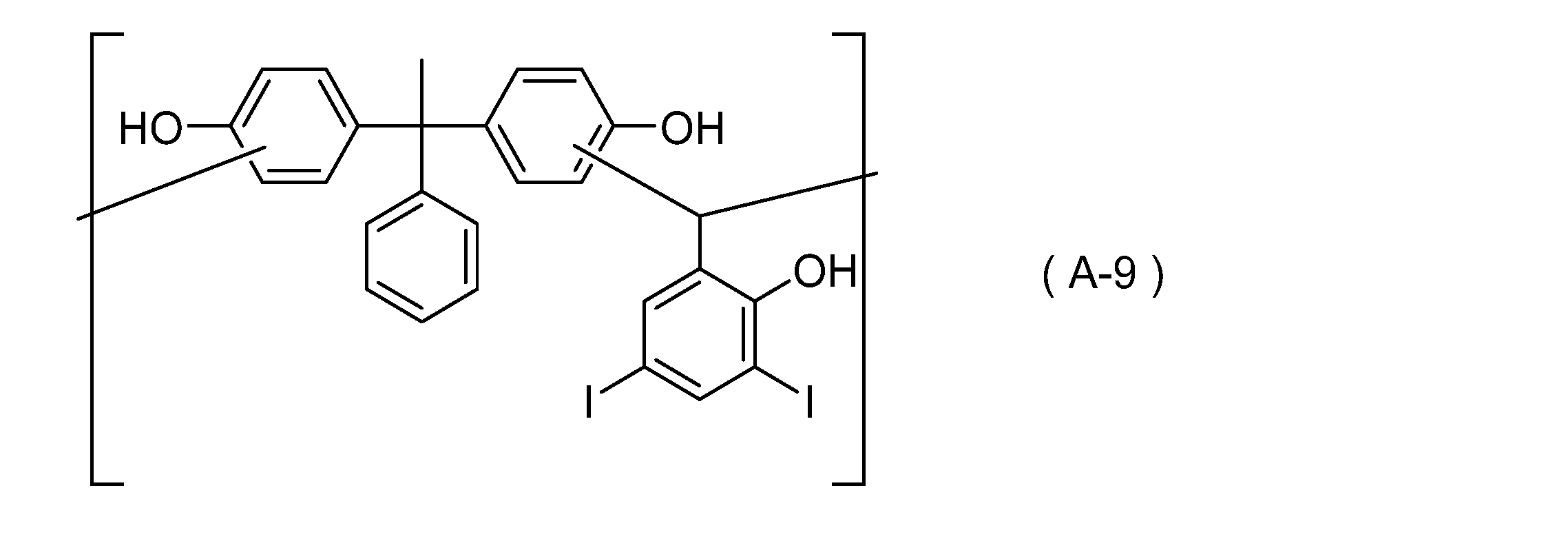
2,7-ジヒドロキシナフタレン10.0gの代わりに、1,1-ビス(4-ヒドロキシフェニル)-1-フェニルエタン18.1gに変えたこと以外は[合成例4]と同様の条件で反応させることにより、下記式(A-9)で表される繰り返し単位を有する重合体(A-9)を得た。重合体(A-9)のMwは2890であった。
2,7-ジヒドロキシナフタレン10.0gの代わりに、1-ナフトール9.0gに変えたこと以外は[合成例3]と同様の条件で反応させることにより、下記式(A-10)で表される繰り返し単位を有する重合体(A-10)を得た。重合体(A-10)のMwは2000であった。
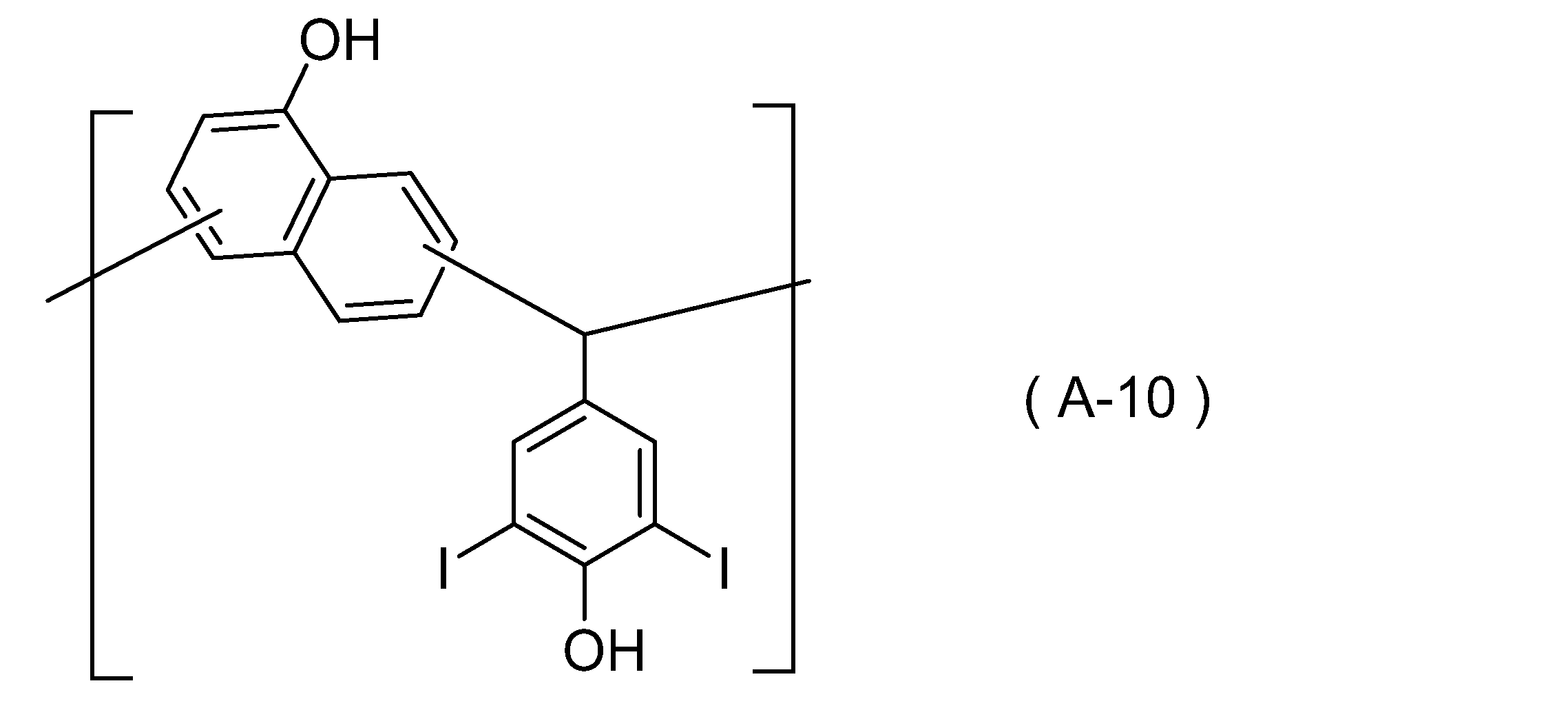
2,7-ジヒドロキシナフタレン10.0gの代わりに、9,9-ビス(4-ヒドロキシフェニル)フルオレン21.9gに変えたこと以外は[合成例3]と同様の条件で反応させることにより、下記式(A-11)で表される繰り返し単位を有する重合体(A-11)を得た。重合体(A-11)のMwは3100であった。
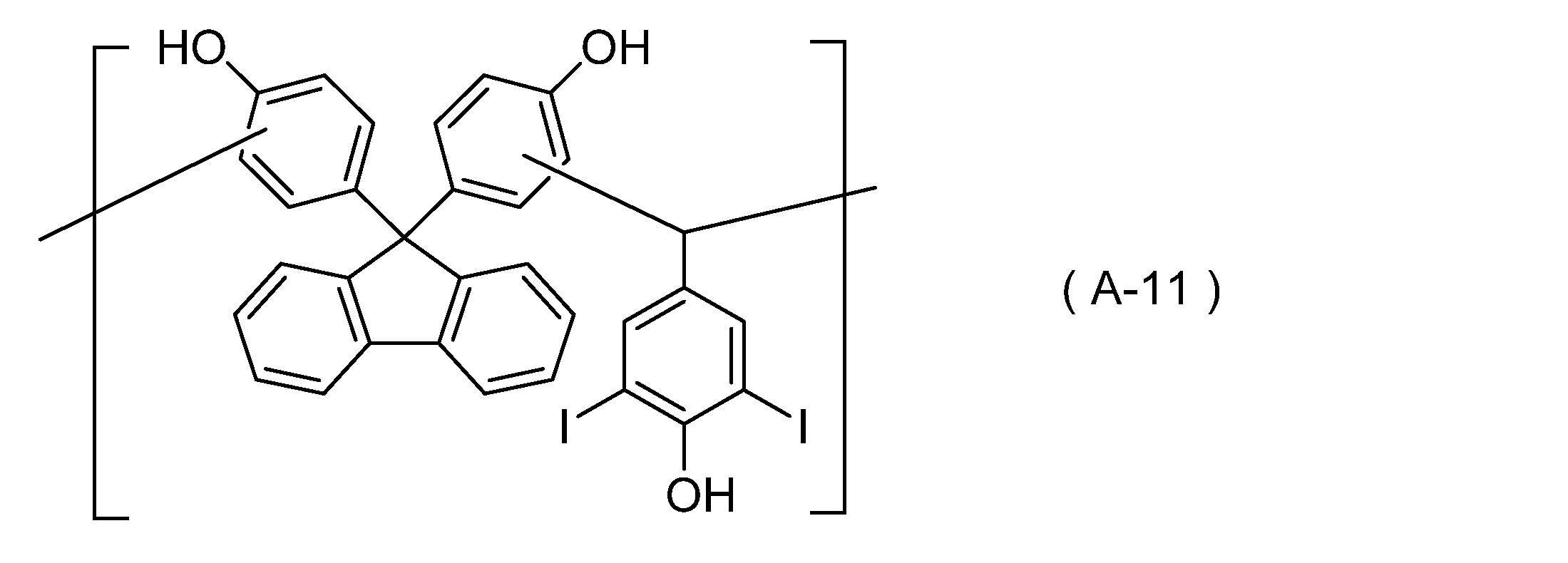
2,7-ジヒドロキシナフタレン10.0gの代わりに、m-クレゾール6.8gに変えたこと以外は[合成例3]と同様の条件で反応させることにより、下記式(A-12)で表される繰り返し単位を有する重合体(A-12)を得た。重合体(A-12)のMwは1980であった。

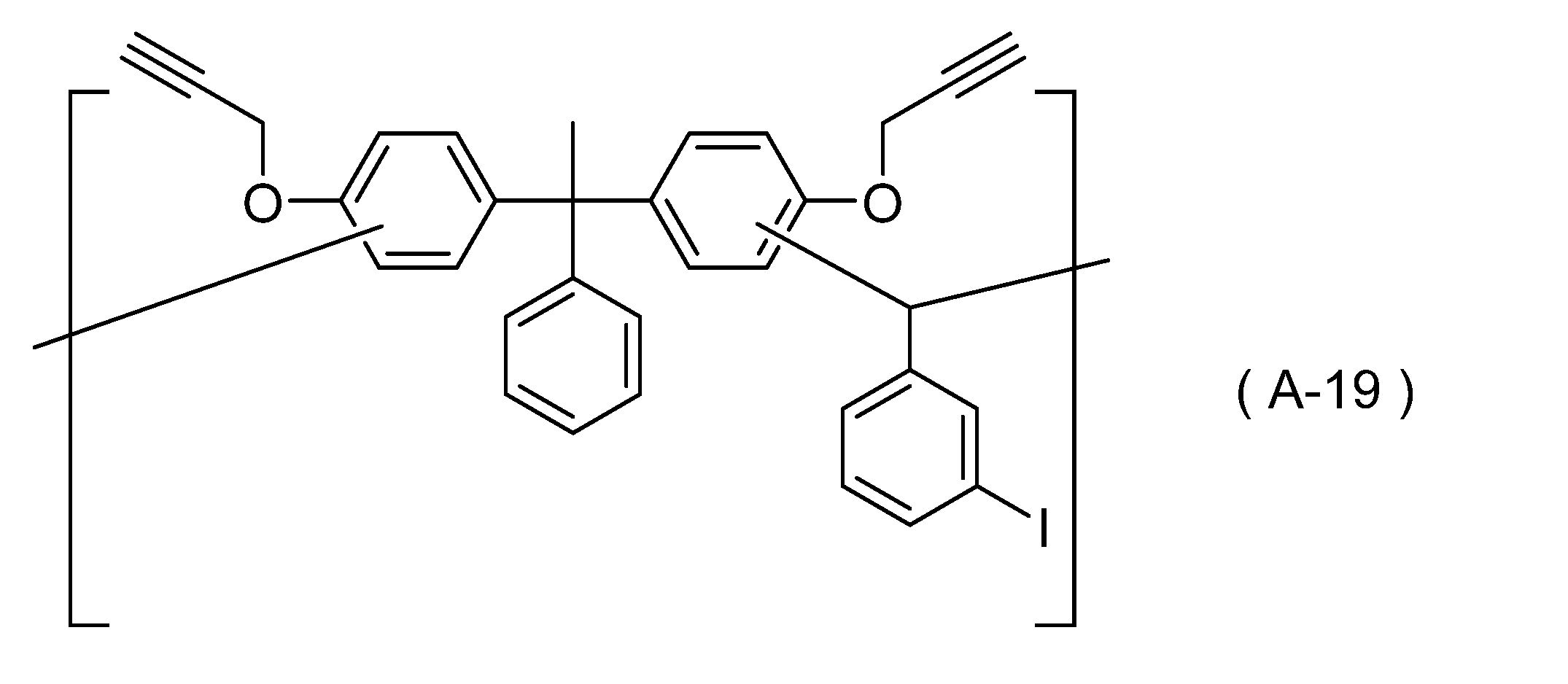
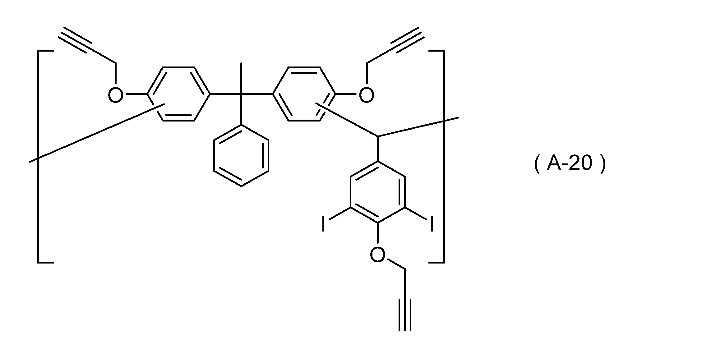
反応容器に重合体(A-1)5.0g、メチルイソブチルケトン30.0g、メタノール12.0g、テトラメチルアンモニウムヒドロキシド(25%水溶液)12.0gを加えて、室温で数分間攪拌させることで重合体(A-1)を溶解させた。臭化プロパルギル3.8gを添加し、室温から40℃に加熱して4時間反応させた。反応終了後、反応溶液を分液ロートに移し、メチルイソブチルケトン100gと5%シュウ酸水溶液200gを加えて有機相を分離した。有機相を数回水で洗浄した後、得られた有機相をエバポレーターで濃縮し、メタノール150g中に滴下させて沈殿物を得た。沈殿物を吸引濾過により回収し、メタノール50gで数回洗浄した。その後、真空乾燥機内にて60℃で12時間乾燥することにより、下記式(A-13)で表される繰り返し単位を有する重合体(A-13)を得た。重合体(A-13)のMwは3115であり、重合体(A-13)におけるプロパルギル基の導入率は、全ヒドロキシ基に対して83%であった。

重合体(A-1)5.0gの代わりに、重合体(A-2)5.0gに変えたこと以外は[合成例13]と同様の条件で反応させることにより、下記式(A-14)で表される繰り返し単位を有する重合体(A-14)を得た。重合体(A-14)のMwは3520であり、重合体(A-14)におけるプロパルギル基の導入率は、全ヒドロキシ基に対して90%であった。
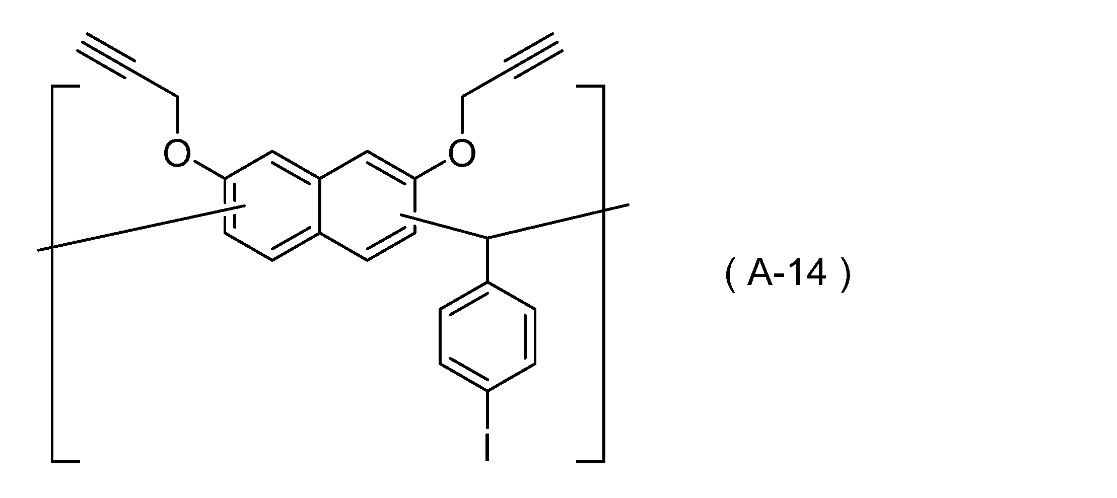
重合体(A-1)5.0gの代わりに、重合体(A-3)6.9gに変えたこと以外は[合成例13]と同様の条件で反応させることにより、下記式(A-15)で表される繰り返し単位を有する重合体(A-15)を得た。重合体(A-15)のMwは3700であり、重合体(A-15)におけるプロパルギル基の導入率は、全ヒドロキシ基に対して87%であった。
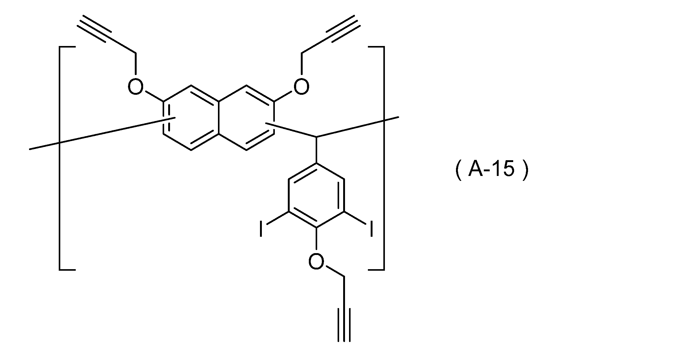
重合体(A-1)5.0gの代わりに、重合体(A-4)6.9gに変えたこと以外は[合成例13]と同様の条件で反応させることにより、下記式(A-16)で表される繰り返し単位を有する重合体(A-16)を得た。重合体(A-16)のMwは4070であり、重合体(A-16)におけるプロパルギル基の導入率は、全ヒドロキシ基に対して76%であった。
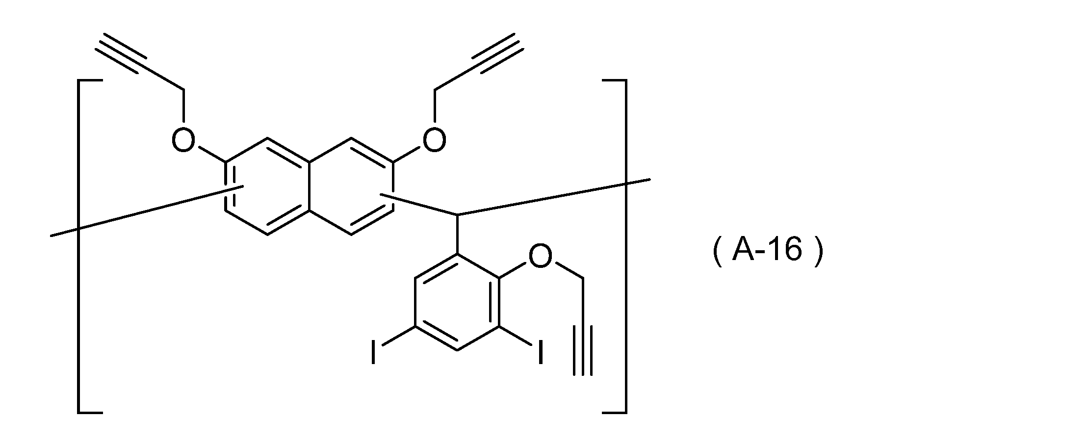
重合体(A-1)5.0gの代わりに、重合体(A-5)5.8gに変えたこと以外は[合成例13]と同様の条件で反応させることにより、下記式(A-17)で表される繰り返し単位を有する重合体(A-17)を得た。重合体(A-17)のMwは3960であり、重合体(A-17)におけるプロパルギル基の導入率は、全ヒドロキシ基に対して71%であった。
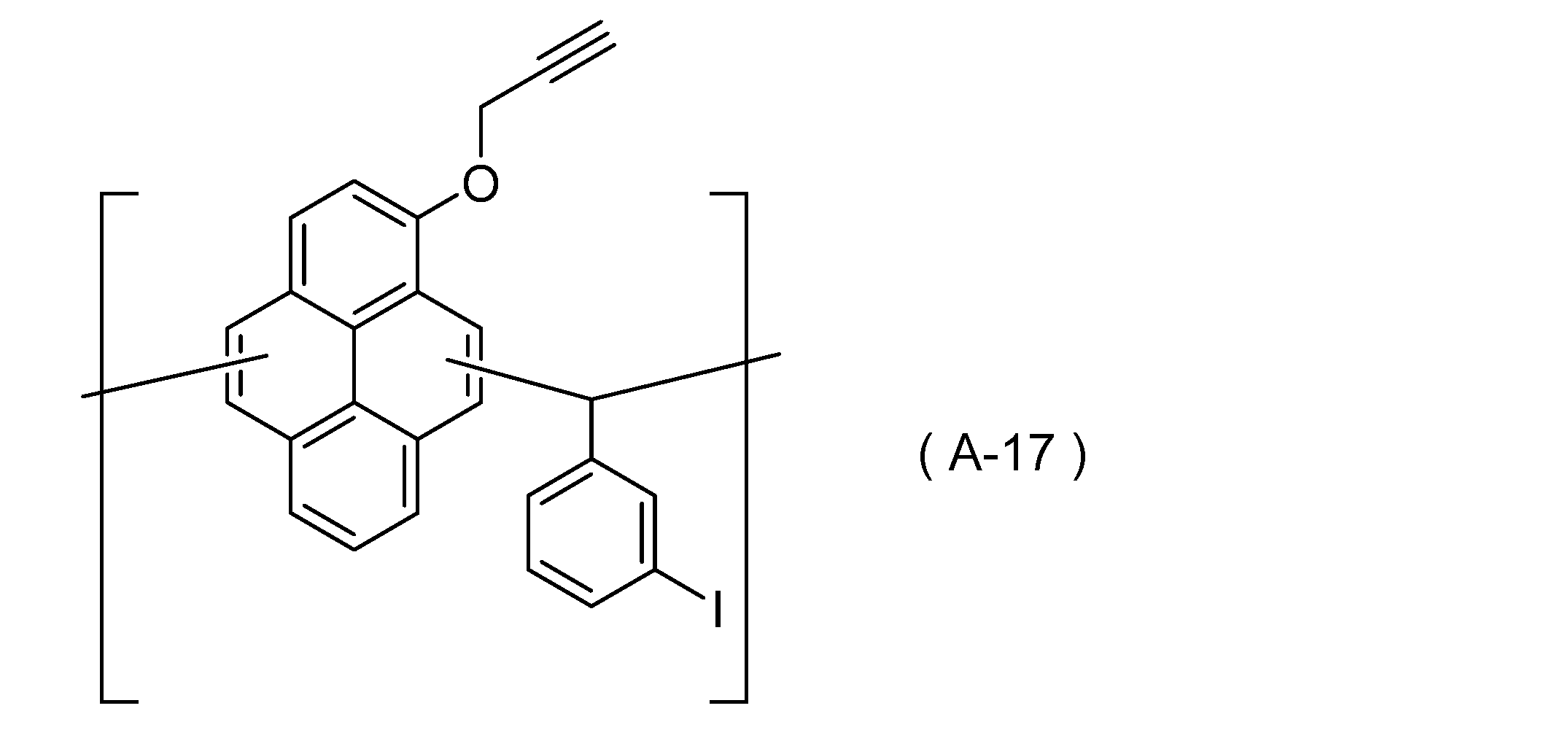
重合体(A-1)5.0gの代わりに、重合体(A-6)7.7gに変えたこと以外は[合成例13]と同様の条件で反応させることにより、下記式(A-18)で表される繰り返し単位を有する重合体(A-18)を得た。重合体(A-18)のMwは3835であり、重合体(A-18)におけるプロパルギル基の導入率は、全ヒドロキシ基に対して92%であった。

重合体(A-1)5.0gの代わりに、重合体(A-7)6.8gに変えたこと以外は[合成例13]と同様の条件で反応させることにより、下記式(A-19)で表される繰り返し単位を有する重合体(A-19)を得た。重合体(A-19)のMwは4110であり、重合体(A-19)におけるプロパルギル基の導入率は、全ヒドロキシ基に対して78%であった。
重合体(A-1)5.0gの代わりに、重合体(A-8)8.7gに変えたこと以外は[合成例13]と同様の条件で反応させることにより、下記式(A-20)で表される繰り返し単位を有する重合体(A-20)を得た。重合体(A-20)のMwは2900であり、重合体(A-20)におけるプロパルギル基の導入率は、全ヒドロキシ基に対して90%であった。
重合体(A-1)5.0gの代わりに、重合体(A-9)8.7gに変えたこと以外は[合成例13]と同様の条件で反応させることにより、下記式(A-21)で表される繰り返し単位を有する重合体(A-21)を得た。重合体(A-21)のMwは3750であり、重合体(A-21)におけるプロパルギル基の導入率は、全ヒドロキシ基に対して81%であった。
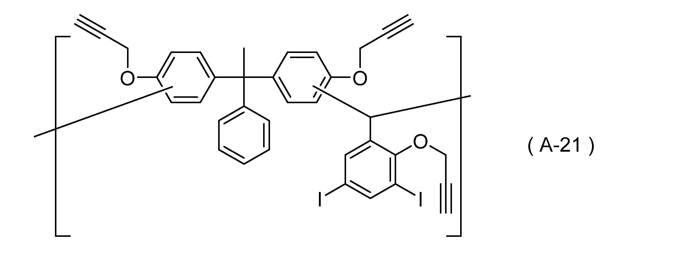
重合体(A-1)5.0gの代わりに、重合体(A-10)6.7gに変えたこと以外は[合成例13]と同様の条件で反応させることにより、下記式(A-22)で表される繰り返し単位を有する重合体(A-22)を得た。重合体(A-22)のMwは4290であり、重合体(A-22)におけるプロパルギル基の導入率は、全ヒドロキシ基に対して70%であった。
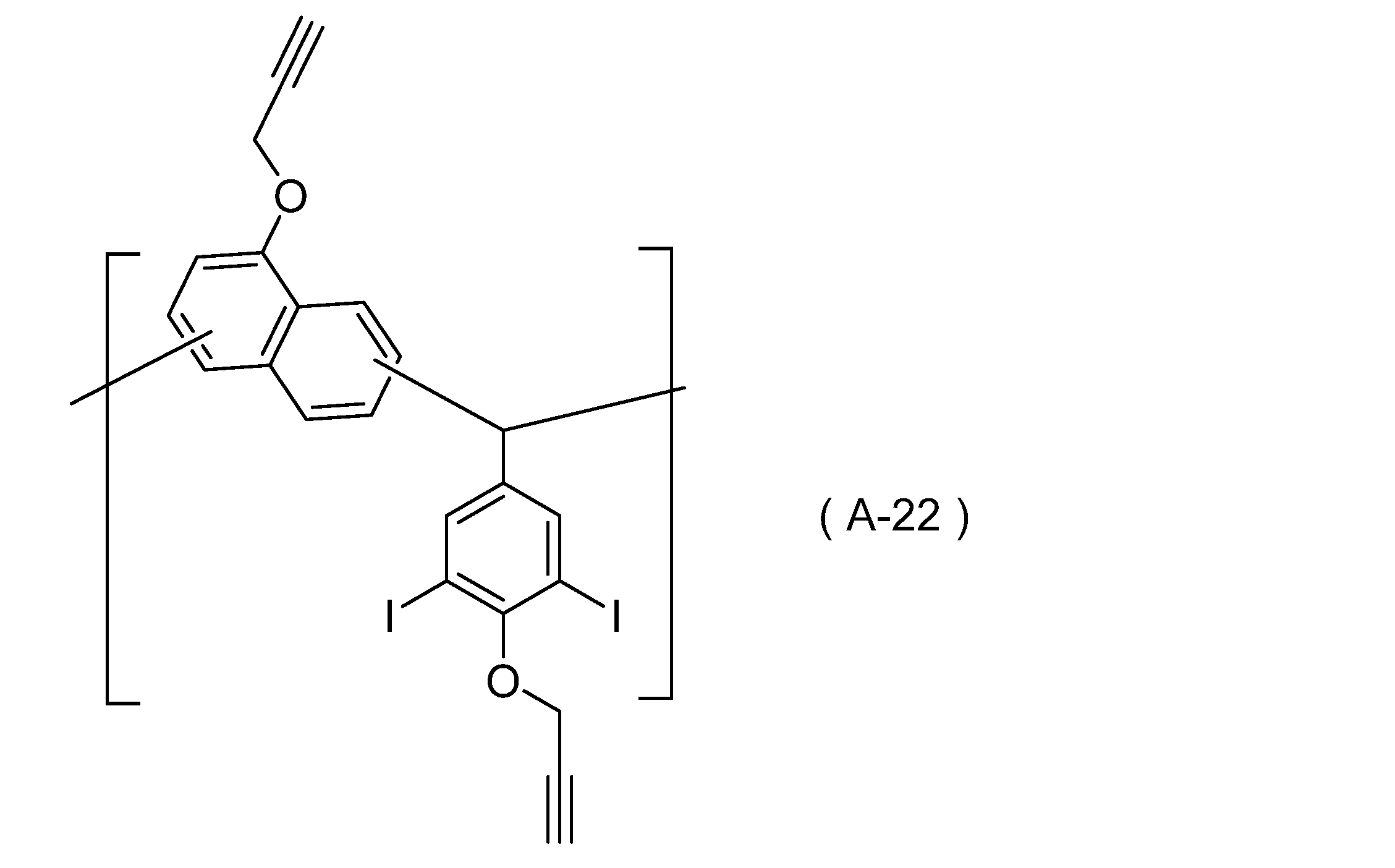
重合体(A-1)5.0gの代わりに、重合体(A-11)9.5gに変えたこと以外は[合成例13]と同様の条件で反応させることにより、下記式(A-23)で表される繰り返し単位を有する重合体(A-23)を得た。重合体(A-23)のMwは4300であり、重合体(A-23)におけるプロパルギル基の導入率は、全ヒドロキシ基に対して74%であった。

重合体(A-1)5.0gの代わりに、重合体(A-12)6.2gに変えたこと以外は[合成例13]と同様の条件で反応させることにより、下記式(A-24)で表される繰り返し単位を有する重合体(A-24)を得た。重合体(A-24)のMwは2290であり、重合体(A-24)におけるプロパルギル基の導入率は、全ヒドロキシ基に対して77%であった。

反応容器に、窒素雰囲気下、1,3,5-ベンゼントリイルトリス-9H-フルオレン10.0g、3-ヨードベンズアルデヒド22.7gおよびテトラヒドロフラン140.0gを加えて懸濁させた。25%テトラメチルアンモニウムヒドロキシド46.0gおよびテトラブチルアンモニウムブロミド1.7gを加え、60℃で4時間反応させた。反応終了後、メチルイソブチルケトン300.0gと5%シュウ酸水溶液200.0gを加えて有機相を分離した。有機相を数回水で洗浄した後、得られた有機相をエバポレーターで濃縮し、メタノール300g中に滴下させて沈殿物を得た。沈殿物を吸引濾過により回収し、メタノール50.0gで数回洗浄した。その後、真空乾燥機内にて60℃で12時間乾燥することにより、下記式(A-25)で表される化合物(A-25)を得た。

反応容器に、窒素雰囲気下、1,3,5-ベンゼントリイルトリス-9H-フルオレン10.0g、3,5-ジヨード-4-ヒドロキシベンズアルデヒド36.7gおよびテトラヒドロフラン180.0gを加えて懸濁させた。1,8-ジアザビシクロ[5.4.0]-7-ウンデセン2.6gを加え、100℃で8時間反応させた。反応終了後、メチルイソブチルケトン300.0gと5%シュウ酸水溶液200.0gを加えて有機相を分離した。有機相を数回水で洗浄した後、得られた有機相をエバポレーターで濃縮し、メタノール300g中に滴下させて沈殿物を得た。沈殿物を吸引濾過により回収し、メタノール50.0gで数回洗浄した。その後、真空乾燥機内にて60℃で12時間乾燥させた。得られた化合物10.0gにメチルイソブチルケトン50.0g、メタノール20.0g、テトラメチルアンモニウムヒドロキシド(25%水溶液)7.3gを加えて、室温で数分間攪拌させた。臭化プロパルギル2.4gを添加し、室温から40℃に加熱して4時間反応させた。反応終了後、反応溶液を分液ロートに移し、メチルイソブチルケトン200gと5%シュウ酸水溶液200gを加えて有機相を分離した。有機相を数回水で洗浄した後、得られた有機相をエバポレーターで濃縮し、メタノール300g中に滴下させて沈殿物を得た。沈殿物を吸引濾過により回収し、メタノール50gで数回洗浄した。その後、真空乾燥機内にて60℃で12時間乾燥することにより、下記式(A-26)で表される化合物(A-26)を得た。化合物(A-26)におけるプロパルギル基の導入率は、全ヒドロキシ基に対して82%であった。
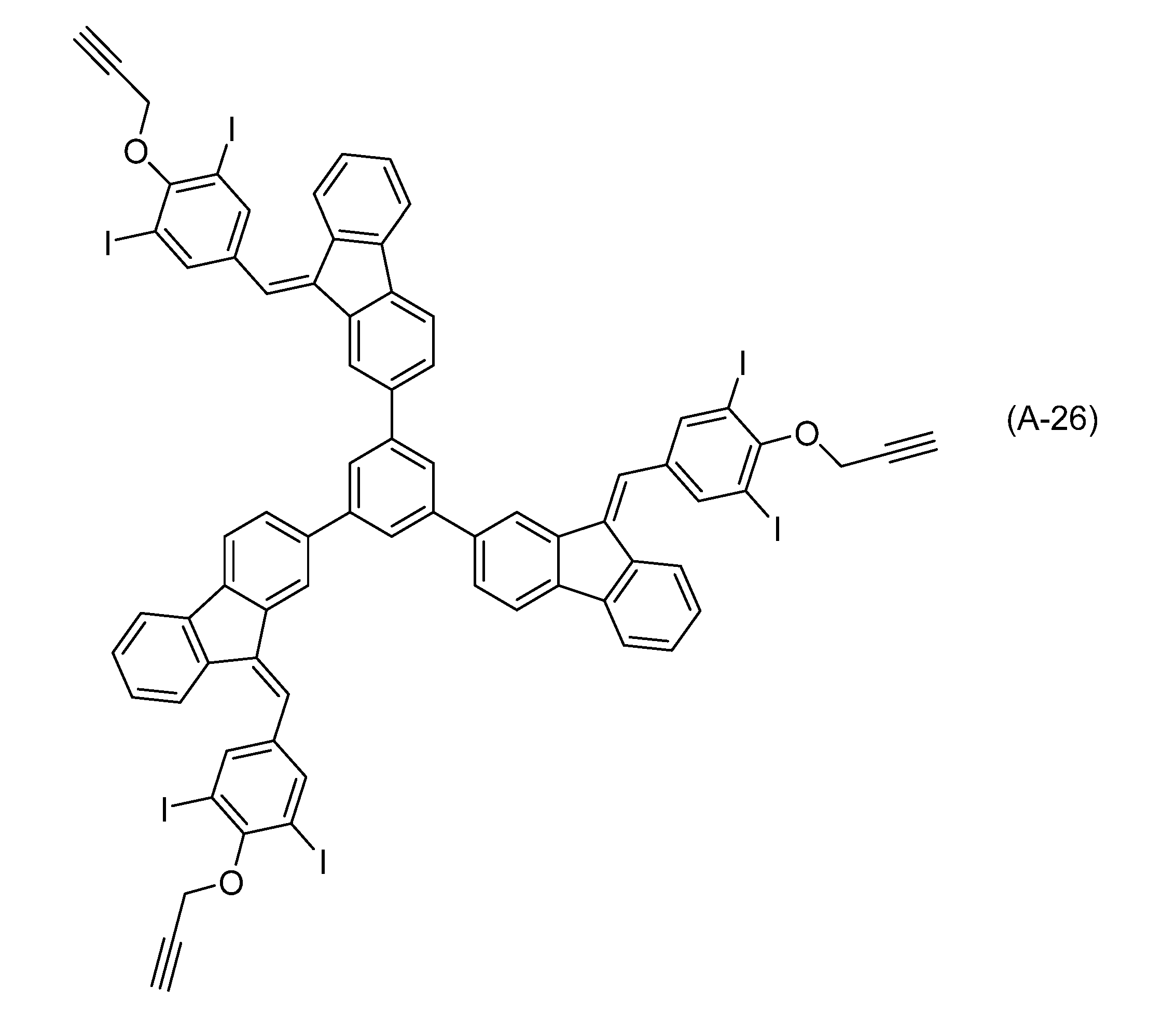
3-ヨードベンズアルデヒド22.7gの代わりに、3-ヨードベンズアルデヒド11.3gと3-エチニルベンズアルデヒド6.4gの混合物に変えたこと以外は[合成例25]と同様の条件で反応させることにより、下記式(A-27)で表される化合物(A-27)を得た。式中、Rを示す構造に添えた数字は化合物(A-27)中でのモル比を表す。

3,5-ジヨード-4-ヒドロキシベンズアルデヒド36.7gの代わりに、3-ヨードベンズアルデヒド11.3gと3-ヒドロキシベンズアルデヒド6.0gの混合物に変えたこと以外は[合成例26]と同様の条件で反応させることにより、下記式(A-28)で表される化合物(A-28)を得た。式中、Rを示す構造に添えた数字は化合物(A-28)中でのモル比を表す。化合物(A-28)におけるプロパルギル基の導入率は、全ヒドロキシ基に対して92%であった。

反応容器に、窒素雰囲気下、メタクリル酸グリシジル7.0g、2,2’-アゾビス(2,4-ジメチルバレロニトリル)1.6gおよびメチルイソブチルケトン2.0gを加えて、均一に溶解させた。その後、80℃まで昇温させ6時間加熱することで反応させた。得られた反応液をヘキサン120g中に滴下させて沈殿物を得た。沈殿物を吸引濾過により回収し、ヘキサン50gで数回洗浄した。その後、真空乾燥機内にて60℃で12時間乾燥することにより、メタクリル酸グリシジルのホモポリマーを得た(Mw=2870)。得られたポリマー5.0gをメチルイソブチルケトン20.0gに溶解させた。4-ヨード安息香酸11.3gおよび25%テトラメチルアンモニウムヒドロキシド2.6gを加え、80℃で6時間反応させた。反応終了後、メチルイソブチルケトン100.0gと5%シュウ酸水溶液100.0gを加えて有機相を分離した。有機相を数回水で洗浄した後、得られた有機相をエバポレーターで濃縮し、ヘキサン100g中に滴下させて沈殿物を得た。沈殿物を吸引濾過により回収し、ヘキサン50.0gで数回洗浄した。その後、真空乾燥機内にて60℃で12時間乾燥することにより、下記式(X-1)で表される重合体(X-1)を得た。重合体(X-1)のMwは4420であった。
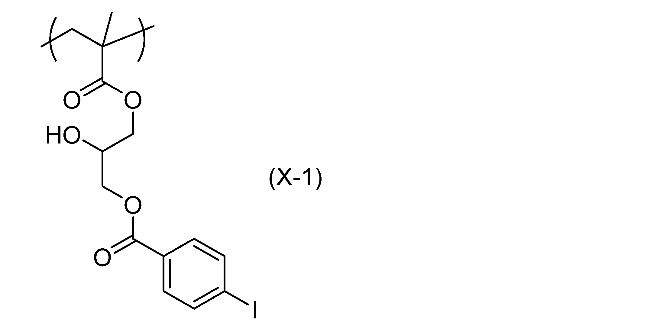
組成物の調製に用いた[A]化合物、[B]溶媒、[C]酸発生剤、[D]架橋剤及び[E]その他の成分について以下に示す。
実施例:上記重合体(A-1)~(A-24)、化合物(A-25)~(A-28)
比較例:上記重合体(X-1)
B-1:酢酸プロピレングリコールモノメチルエーテル
C-1:下記式(C-1)で表される化合物)

D-1:下記式(D-1)で表される化合物

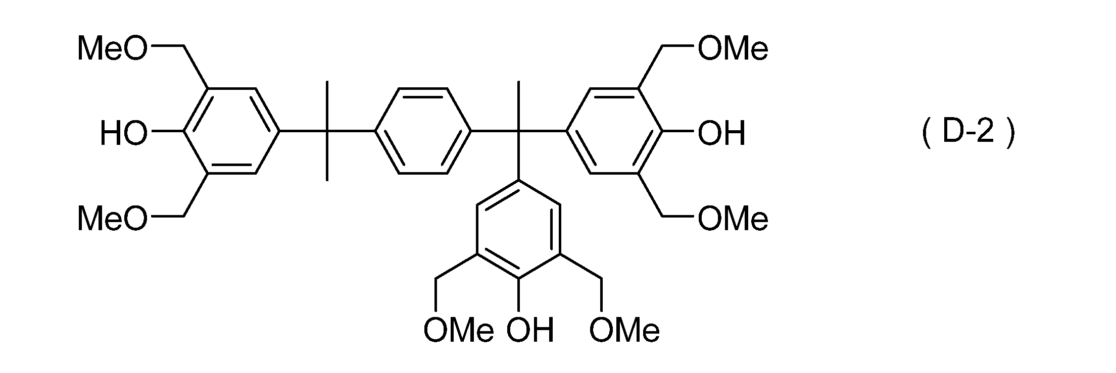
E-1:下記式(E-1)で表される繰り返し単位を有する重合体(Mw:1500)
E-2:下記式(E-2)で表される繰り返し単位を有する重合体(Mw:1800)
E-3:下記式(E-3)で表される化合物

[A]化合物としての(A-1)2質量部、[C]酸発生剤としての(C-1)0.05質量部及び[D]架橋剤としての(D-1)0.05質量部を[B]溶媒としての(B-1)97.9質量部に溶解した。得られた溶液を孔径0.45μmのポリテトラフルオロエチレン(PTFE)メンブランフィルターでろ過して、組成物(J-1)を調製した。
下記表1に示す種類及び含有量の各成分を使用したこと以外は、実施例1と同様にして組成物(J-2)~(J-30)及び(CJ-1)を調製した。表1中の「[C]酸発生剤」及び「[D]架橋剤」の列における「-」は、該当する成分を使用しなかったことを示す。

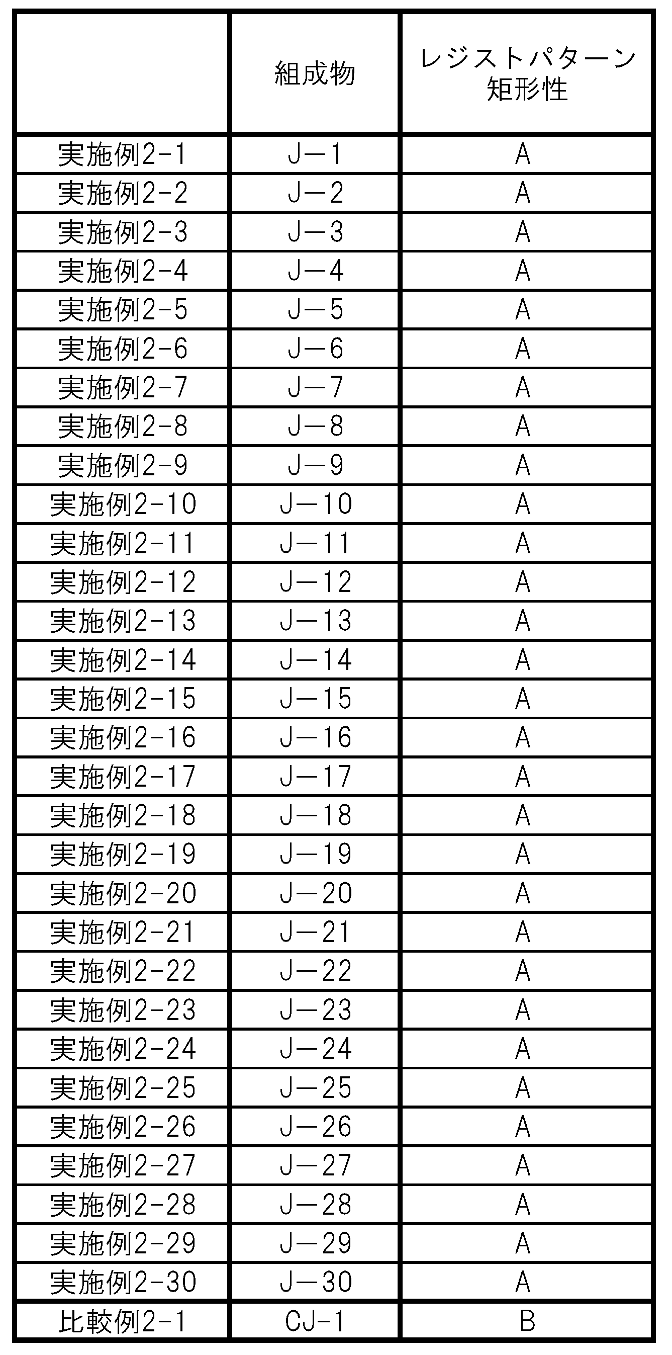
上記調製したレジスト下層膜形成用組成物を用いて、以下の方法により、レジストパターンの矩形性を評価した。評価結果を下記表2に示す。
レジスト組成物(R-1)は、4-ヒドロキシスチレンに由来する構造単位(1)、スチレンに由来する構造単位(2)及び4-t-ブトキシスチレンに由来する構造単位(3)(各構造単位の含有割合は、(1)/(2)/(3)=65/5/30(モル%))を有する重合体100質量部と、感放射線性酸発生剤としてのトリフェニルスルホニウムトリフルオロメタンスルホネート1.0質量部と、溶媒としての乳酸エチル4,400質量部及びプロピレングリコールモノメチルエーテルアセテート1,900質量部とを混合し、得られた溶液を孔径0.2μmのポリテトラフルオロエチレン(PTFE)メンブランフィルターでろ過することで得た。
12インチシリコンウェハ上に、有機下層膜形成用材料(JSR(株)の「HM8006」)をスピンコーター(東京エレクトロン(株)の「CLEAN TRACK ACT12」)による回転塗工法により塗工した後、250℃で60秒間加熱を行うことにより平均厚み100nmの有機下層膜を形成した。この有機下層膜上に、ケイ素含有膜形成用組成物(JSR(株)の「NFC SOG080」)を塗工し、220℃で60秒間加熱した後、23℃で30秒間冷却することにより平均厚み20nmのケイ素含有膜を形成した。上記形成したケイ素含有膜上に、上記調製したレジスト下層膜形成用組成物を塗工し、250℃で60秒間加熱した後、23℃で30秒間冷却することにより平均厚み5nmのレジスト下層膜を形成した。上記形成したレジスト下層膜上に、レジスト組成物(R-1)を塗工し、130℃で60秒間加熱した後、23℃で30秒間冷却することにより平均厚み50nmのレジスト膜を形成した。次いで、EUVスキャナー(ASML社の「TWINSCAN NXE:3300B」(NA0.3、シグマ0.9、クアドルポール照明、ウェハ上寸法が線幅16nmの1対1ラインアンドスペースのマスク)を用いてレジスト膜に極端紫外線を照射した。極端紫外線の照射後、基板を110℃で60秒間加熱を行い、次いで23℃で60秒間冷却した。その後、2.38質量%のテトラメチルアンモニウムヒドロキシド水溶液(20℃~25℃)を用い、パドル法により現像した後、水で洗浄し、乾燥することにより、レジストパターンが形成された評価用基板を得た。上記評価用基板のレジストパターンの測長及び観察には走査型電子顕微鏡((株)日立ハイテクの「SU8220」)を用いた。レジストパターン矩形性は、パターンの断面形状が矩形である場合を「A」(良好)と、パターンの断面に裾引きがある場合を「B」(不良)と評価した。
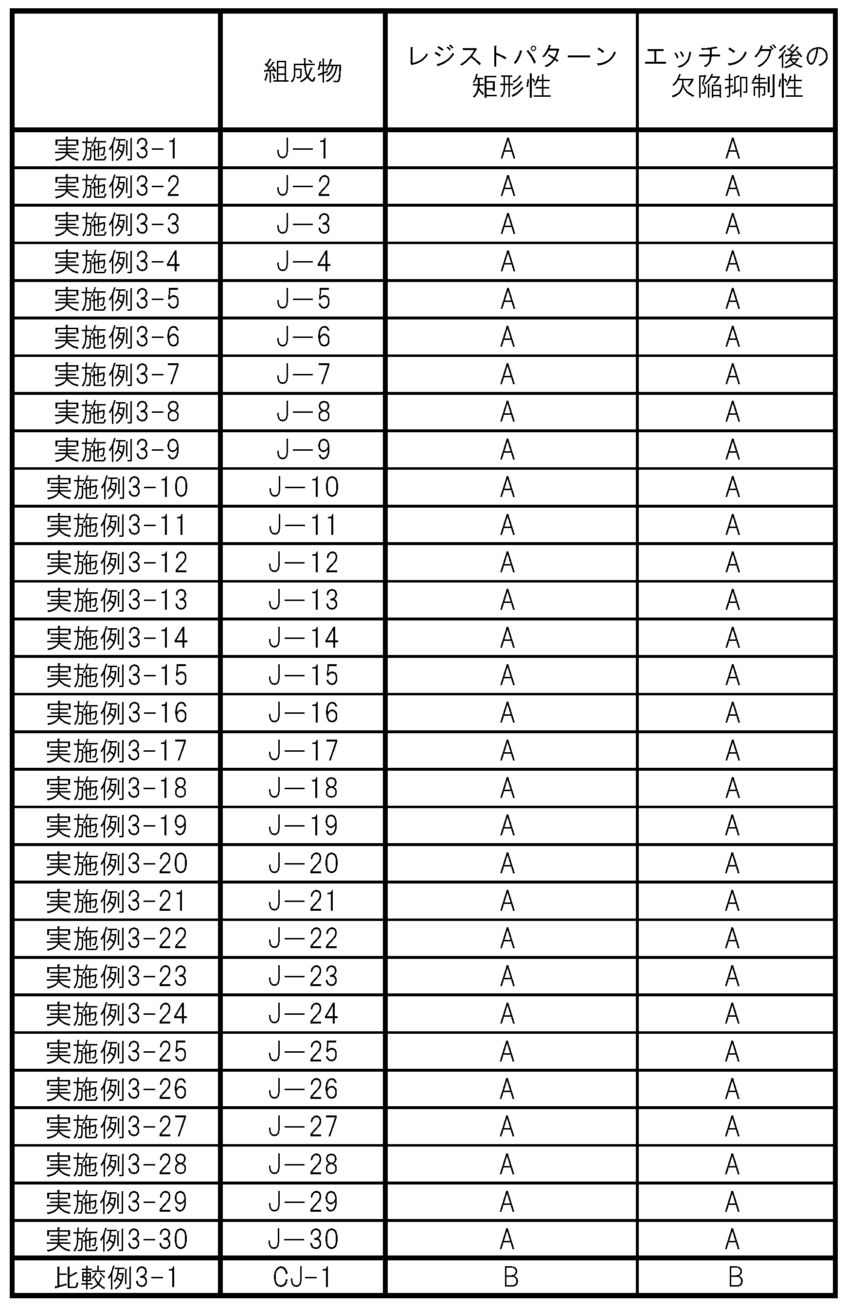
上記調製したレジスト下層膜形成用組成物を用いて、以下の方法により、レジストパターンの矩形性及びエッチング後の欠陥抑制性を評価した。評価結果を下記表3に示す。
レジスト組成物(R-2)の調製に用いる化合物(S-1)を、以下に示す手順により合成した。反応容器内において、150mLの0.5N水酸化ナトリウム水溶液を攪拌しながら、イソプロピルスズ三塩化物6.5質量部を添加し、反応を2時間実施した。析出した沈殿物をろ取し、50質量部の水で2回洗浄した後、乾燥させ、化合物(S-1)を得た。化合物(S-1)は、イソプロピルスズ三塩化物の加水分解物の酸化水酸化物生成物(i-PrSnO(3/2-x/2)(OH)x(0<x<3)を構造単位とする)であった。
12インチシリコンウェハ上に、有機下層膜形成用材料(JSR(株)の「HM8006」)をスピンコーター(東京エレクトロン(株)の「CLEAN TRACK ACT12」)による回転塗工法により塗工した後、250℃で60秒間加熱を行うことにより平均厚み100nmの有機下層膜を形成した。この有機下層膜上に、上記調製したレジスト下層膜形成用組成物を塗工し、220℃で60秒間加熱した後、23℃で30秒間冷却することにより平均厚み5nmのレジスト下層膜を形成した。このレジスト下層膜上に、レジスト組成物(R-2)を、上記スピンコーターによる回転塗工法により塗工し、所定の時間経過後に、90℃で60秒間加熱してから、23℃で30秒間冷却することにより平均厚み35nmのレジスト膜を形成した。EUVスキャナー(ASML社の「TWINSCAN NXE:3300B」(NA0.3、シグマ0.9、クアドルポール照明、ウェハ上寸法が線幅25nmの1対1ラインアンドスペースのマスク)を用いてレジスト膜に露光を行った。露光後、基板を110℃で60秒間加熱し、次いで23℃で60秒間冷却した。その後、2-ヘプタノン(20~25℃)を用い、パドル法により現像した後、乾燥することにより、レジストパターンが形成された評価用基板を得た。上記評価用基板のレジストパターンの測長及び観察には走査型電子顕微鏡((株)日立ハイテクの「SU8220」)を用いた。レジストパターン矩形性は、パターンの断面形状が矩形である場合を「A」(良好)と、パターンの断面形状に裾引きがある場合を「B」(不良)と評価した。
上記レジスト組成物(R-2)によるレジストパターンが形成された評価用基板を、エッチング装置(東京エレクトロン社の「TACTRAS」)を用いて、O2=400sccm、PRESS.=25MT、HF RF=400W、LF RF=0W、DCS=0V、RDC=50%条件にて処理を行い、上記レジストパターンをマスクとして上記レジスト下層膜を選択的に除去した評価用基板を得た。上記評価用基板のパターンの観察には走査型電子顕微鏡((株)日立ハイテクの「SU8220」)を用いた。エッチング後の欠陥抑制性は、レジスト下層膜パターンの断面において、選択的にレジスト下層膜を除去した部分に残渣(欠陥)が無い場合を「A」(良好)と、残渣(欠陥)がある場合を「B」(不良)と評価した。
Claims (12)
- 極端紫外線での露光に供されるレジスト膜の下層膜形成用組成物であって、
ヨウ素原子を有する化合物と、
溶媒と
を含み、
上記ヨウ素原子を有する化合物が、下記式(1)で表される繰り返し単位を有する重合体、ヨウ素原子を有する分子量が750以上3000以下の芳香環含有化合物又はこれらの組み合わせであり、
上記下層膜形成用組成物における溶媒以外の成分に占める上記ヨウ素原子を有する化合物の含有割合が50質量%以上である、レジスト下層膜形成用組成物。

- 上記R1が環員数5~40の芳香環を有する、請求項1に記載のレジスト下層膜形成用組成物。
- 上記芳香環の水素原子の少なくとも1つがヨウ素原子で置換されている、請求項2に記載のレジスト下層膜形成用組成物。
- 上記芳香環が、ベンゼン環、ナフタレン環、アントラセン環、フェナレン環、フェナントレン環、ピレン環、フルオレン環及びペリレン環からなる群より選ばれる少なくとも1つの芳香族炭化水素環である、請求項1~3のいずれか1項に記載のレジスト下層膜形成用組成物。
- 上記ヨウ素原子を有する化合物は、ヒドロキシ基、下記式(2-1)で表される基及び下記式(2-2)で表される基からなる群より選ばれる少なくとも1つの基を有する、請求項1~3のいずれか1項に記載のレジスト下層膜形成用組成物。
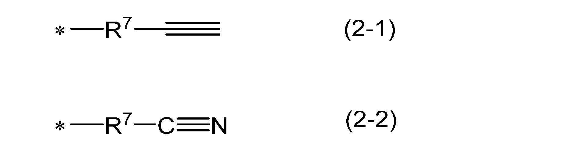
- 金属含有レジスト膜の下層膜形成用である、請求項1~3のいずれか1項に記載のレジスト下層膜形成用組成物。
- 基板に直接又は間接にレジスト下層膜形成用組成物を塗工する工程と、
上記レジスト下層膜形成用組成物塗工工程により形成されたレジスト下層膜にレジスト膜形成用組成物を塗工する工程と、
上記レジスト膜形成用組成物塗工工程により形成されたレジスト膜を極端紫外線により露光する工程と、
少なくとも上記露光されたレジスト膜を現像する工程と
を備え、
上記レジスト下層膜形成用組成物が、
ヨウ素原子を有する化合物と、
溶媒と
を含み、
上記ヨウ素原子を有する化合物が、下記式(1)で表される繰り返し単位を有する重合体、ヨウ素原子を有する分子量が750以上3000以下の芳香環含有化合物又はこれらの組み合わせであり、
上記下層膜形成用組成物における溶媒以外の成分に占める上記ヨウ素原子を有する化合物の含有割合が50質量%以上である、半導体基板の製造方法。

- 上記R1が環員数5~40の芳香環を有する、請求項7に記載の半導体基板の製造方法。
- 上記芳香環の水素原子の少なくとも1つがヨウ素原子で置換されている、請求項8に記載の半導体基板の製造方法。
- 上記芳香環が、ベンゼン環、ナフタレン環、アントラセン環、フェナレン環、フェナントレン環、ピレン環、フルオレン環及びペリレン環からなる群より選ばれる少なくとも1つの芳香族炭化水素環である、請求項7~9のいずれか1項に記載の半導体基板の製造方法。
- 上記ヨウ素原子を有する化合物は、ヒドロキシ基、下記式(2-1)で表される基及び下記式(2-2)で表される基からなる群より選ばれる少なくとも1つの基を有する、請求項7~9のいずれか1項に記載の半導体基板の製造方法。

- 上記レジスト膜が金属を含有する、請求項7~9のいずれか1項に記載の半導体基板の製造方法。
Priority Applications (3)
| Application Number | Priority Date | Filing Date | Title |
|---|---|---|---|
| JP2024550107A JPWO2024070786A1 (ja) | 2022-09-30 | 2023-09-19 | |
| KR1020257009374A KR20250085723A (ko) | 2022-09-30 | 2023-09-19 | 레지스트 하층막 형성용 조성물 및 반도체 기판의 제조 방법 |
| US19/093,450 US20250251666A1 (en) | 2022-09-30 | 2025-03-28 | Resist underlayer film-forming composition, and method for manufacturing semiconductor substrate |
Applications Claiming Priority (2)
| Application Number | Priority Date | Filing Date | Title |
|---|---|---|---|
| JP2022-157452 | 2022-09-30 | ||
| JP2022157452 | 2022-09-30 |
Related Child Applications (1)
| Application Number | Title | Priority Date | Filing Date |
|---|---|---|---|
| US19/093,450 Continuation-In-Part US20250251666A1 (en) | 2022-09-30 | 2025-03-28 | Resist underlayer film-forming composition, and method for manufacturing semiconductor substrate |
Publications (1)
| Publication Number | Publication Date |
|---|---|
| WO2024070786A1 true WO2024070786A1 (ja) | 2024-04-04 |
Family
ID=90477456
Family Applications (1)
| Application Number | Title | Priority Date | Filing Date |
|---|---|---|---|
| PCT/JP2023/033814 Ceased WO2024070786A1 (ja) | 2022-09-30 | 2023-09-19 | レジスト下層膜形成用組成物及び半導体基板の製造方法 |
Country Status (5)
| Country | Link |
|---|---|
| US (1) | US20250251666A1 (ja) |
| JP (1) | JPWO2024070786A1 (ja) |
| KR (1) | KR20250085723A (ja) |
| TW (1) | TW202419435A (ja) |
| WO (1) | WO2024070786A1 (ja) |
Cited By (2)
| Publication number | Priority date | Publication date | Assignee | Title |
|---|---|---|---|---|
| WO2024204163A1 (ja) * | 2023-03-31 | 2024-10-03 | 日産化学株式会社 | レジスト下層膜形成用組成物 |
| WO2026064217A1 (en) * | 2024-09-21 | 2026-03-26 | Applied Materials, Inc. | Sulfur based resist hardening |
Citations (6)
| Publication number | Priority date | Publication date | Assignee | Title |
|---|---|---|---|---|
| WO2014038483A1 (ja) * | 2012-09-07 | 2014-03-13 | 日産化学工業株式会社 | リソグラフィー用レジスト上層膜形成組成物及びそれを用いた半導体装置の製造方法 |
| JP2014513312A (ja) * | 2011-02-08 | 2014-05-29 | エイゼット・エレクトロニック・マテリアルズ・ユーエスエイ・コーポレイション | 下層コーティング組成物および微細電子デバイスを製造するための方法 |
| WO2016158457A1 (ja) * | 2015-03-30 | 2016-10-06 | 三菱瓦斯化学株式会社 | 化合物、樹脂、及びそれらの精製方法、リソグラフィー用の下層膜形成材料、下層膜形成用組成物、及び下層膜、並びに、レジストパターン形成方法、及び回路パターン形成方法 |
| WO2017038643A1 (ja) * | 2015-08-31 | 2017-03-09 | 三菱瓦斯化学株式会社 | リソグラフィー用下層膜形成材料、リソグラフィー用下層膜形成用組成物、リソグラフィー用下層膜及びその製造方法、並びにレジストパターン形成方法 |
| WO2020040161A1 (ja) * | 2018-08-24 | 2020-02-27 | 三菱瓦斯化学株式会社 | 化合物、及びそれを含む組成物、並びに、レジストパターンの形成方法及び絶縁膜の形成方法 |
| JP2020084175A (ja) * | 2018-11-21 | 2020-06-04 | 信越化学工業株式会社 | ヨウ素含有熱硬化性ケイ素含有材料、これを含むeuvリソグラフィー用レジスト下層膜形成用組成物、及びパターン形成方法 |
Family Cites Families (1)
| Publication number | Priority date | Publication date | Assignee | Title |
|---|---|---|---|---|
| KR20220137951A (ko) | 2020-02-06 | 2022-10-12 | 미쯔비시 가스 케미칼 컴파니, 인코포레이티드 | 리소그래피용 조성물 및 패턴 형성방법 |
-
2023
- 2023-09-19 JP JP2024550107A patent/JPWO2024070786A1/ja active Pending
- 2023-09-19 WO PCT/JP2023/033814 patent/WO2024070786A1/ja not_active Ceased
- 2023-09-19 KR KR1020257009374A patent/KR20250085723A/ko active Pending
- 2023-09-26 TW TW112136676A patent/TW202419435A/zh unknown
-
2025
- 2025-03-28 US US19/093,450 patent/US20250251666A1/en active Pending
Patent Citations (6)
| Publication number | Priority date | Publication date | Assignee | Title |
|---|---|---|---|---|
| JP2014513312A (ja) * | 2011-02-08 | 2014-05-29 | エイゼット・エレクトロニック・マテリアルズ・ユーエスエイ・コーポレイション | 下層コーティング組成物および微細電子デバイスを製造するための方法 |
| WO2014038483A1 (ja) * | 2012-09-07 | 2014-03-13 | 日産化学工業株式会社 | リソグラフィー用レジスト上層膜形成組成物及びそれを用いた半導体装置の製造方法 |
| WO2016158457A1 (ja) * | 2015-03-30 | 2016-10-06 | 三菱瓦斯化学株式会社 | 化合物、樹脂、及びそれらの精製方法、リソグラフィー用の下層膜形成材料、下層膜形成用組成物、及び下層膜、並びに、レジストパターン形成方法、及び回路パターン形成方法 |
| WO2017038643A1 (ja) * | 2015-08-31 | 2017-03-09 | 三菱瓦斯化学株式会社 | リソグラフィー用下層膜形成材料、リソグラフィー用下層膜形成用組成物、リソグラフィー用下層膜及びその製造方法、並びにレジストパターン形成方法 |
| WO2020040161A1 (ja) * | 2018-08-24 | 2020-02-27 | 三菱瓦斯化学株式会社 | 化合物、及びそれを含む組成物、並びに、レジストパターンの形成方法及び絶縁膜の形成方法 |
| JP2020084175A (ja) * | 2018-11-21 | 2020-06-04 | 信越化学工業株式会社 | ヨウ素含有熱硬化性ケイ素含有材料、これを含むeuvリソグラフィー用レジスト下層膜形成用組成物、及びパターン形成方法 |
Cited By (2)
| Publication number | Priority date | Publication date | Assignee | Title |
|---|---|---|---|---|
| WO2024204163A1 (ja) * | 2023-03-31 | 2024-10-03 | 日産化学株式会社 | レジスト下層膜形成用組成物 |
| WO2026064217A1 (en) * | 2024-09-21 | 2026-03-26 | Applied Materials, Inc. | Sulfur based resist hardening |
Also Published As
| Publication number | Publication date |
|---|---|
| TW202419435A (zh) | 2024-05-16 |
| US20250251666A1 (en) | 2025-08-07 |
| JPWO2024070786A1 (ja) | 2024-04-04 |
| KR20250085723A (ko) | 2025-06-12 |
Similar Documents
| Publication | Publication Date | Title |
|---|---|---|
| JP7836500B2 (ja) | 半導体基板の製造方法及び組成物 | |
| JP7824580B2 (ja) | 半導体基板の製造方法、組成物、重合体及び重合体の製造方法 | |
| US20250251666A1 (en) | Resist underlayer film-forming composition, and method for manufacturing semiconductor substrate | |
| WO2024203160A1 (ja) | 半導体基板の製造方法及びレジスト下層膜形成用組成物 | |
| JP7702974B2 (ja) | 半導体基板の製造方法及び組成物 | |
| JP2023059024A (ja) | 半導体基板の製造方法及び組成物 | |
| TWI911471B (zh) | 半導體基板的製造方法及抗蝕劑底層膜形成用組成物 | |
| WO2025047565A1 (ja) | 半導体基板の製造方法及びレジスト下層膜形成用組成物 | |
| WO2025205091A1 (ja) | 半導体基板の製造方法、組成物及び化合物の製造方法 | |
| WO2025211358A1 (ja) | 半導体基板の製造方法及びレジスト下層膜形成用組成物 | |
| WO2025164408A1 (ja) | 半導体基板の製造方法、レジスト下層膜形成用組成物及び窒素含有化合物の製造方法 | |
| WO2023199851A1 (ja) | 半導体基板の製造方法、組成物及び化合物 | |
| WO2025197551A1 (ja) | 半導体基板の製造方法、レジスト下層膜形成用組成物及び窒素含有化合物の製造方法 | |
| WO2024203153A1 (ja) | レジスト下層膜形成用組成物、半導体基板の製造方法及びレジスト下層膜形成用重合体 | |
| WO2025263206A1 (ja) | 半導体基板の製造方法及び組成物 | |
| WO2026034307A1 (ja) | 半導体基板の製造方法、レジスト下層膜形成用組成物及び窒素含有化合物の製造方法 | |
| WO2024070728A1 (ja) | 半導体基板の製造方法、組成物及び重合体 | |
| WO2024085030A1 (ja) | 半導体基板の製造方法及び組成物 | |
| WO2024142925A1 (ja) | 半導体基板の製造方法、組成物及び重合体 | |
| WO2026004498A1 (ja) | 半導体基板の製造方法、レジスト下層膜形成用組成物及び窒素含有化合物の製造方法 | |
| WO2026063319A1 (ja) | レジスト下層膜形成用組成物、半導体基板の製造方法及び芳香環含有化合物の製造方法 | |
| WO2026042732A1 (ja) | レジスト下層膜形成用組成物、半導体基板の製造方法及び窒素含有化合物の製造方法 | |
| WO2026018782A1 (ja) | 保護膜形成用組成物及び半導体基板の製造方法 | |
| WO2024029292A1 (ja) | 組成物、化合物及び半導体基板の製造方法 | |
| WO2022191062A1 (ja) | 半導体基板の製造方法、組成物、重合体及び重合体の製造方法 |
Legal Events
| Date | Code | Title | Description |
|---|---|---|---|
| 121 | Ep: the epo has been informed by wipo that ep was designated in this application |
Ref document number: 23872014 Country of ref document: EP Kind code of ref document: A1 |
|
| WWE | Wipo information: entry into national phase |
Ref document number: 2024550107 Country of ref document: JP |
|
| NENP | Non-entry into the national phase |
Ref country code: DE |
|
| WWP | Wipo information: published in national office |
Ref document number: 1020257009374 Country of ref document: KR |
|
| 122 | Ep: pct application non-entry in european phase |
Ref document number: 23872014 Country of ref document: EP Kind code of ref document: A1 |