WO2024070650A1 - 多層メタサーフェス構造体の製造方法および多層メタサーフェス構造体 - Google Patents
多層メタサーフェス構造体の製造方法および多層メタサーフェス構造体 Download PDFInfo
- Publication number
- WO2024070650A1 WO2024070650A1 PCT/JP2023/033137 JP2023033137W WO2024070650A1 WO 2024070650 A1 WO2024070650 A1 WO 2024070650A1 JP 2023033137 W JP2023033137 W JP 2023033137W WO 2024070650 A1 WO2024070650 A1 WO 2024070650A1
- Authority
- WO
- WIPO (PCT)
- Prior art keywords
- substrate
- metasurface
- layer
- multilayer
- metasurface structure
- Prior art date
- Legal status (The legal status is an assumption and is not a legal conclusion. Google has not performed a legal analysis and makes no representation as to the accuracy of the status listed.)
- Ceased
Links
Images


Classifications
-
- G—PHYSICS
- G02—OPTICS
- G02B—OPTICAL ELEMENTS, SYSTEMS OR APPARATUS
- G02B3/00—Simple or compound lenses
-
- G—PHYSICS
- G02—OPTICS
- G02B—OPTICAL ELEMENTS, SYSTEMS OR APPARATUS
- G02B5/00—Optical elements other than lenses
-
- G—PHYSICS
- G02—OPTICS
- G02B—OPTICAL ELEMENTS, SYSTEMS OR APPARATUS
- G02B5/00—Optical elements other than lenses
- G02B5/18—Diffraction gratings
-
- H—ELECTRICITY
- H01—ELECTRIC ELEMENTS
- H01P—WAVEGUIDES; RESONATORS, LINES, OR OTHER DEVICES OF THE WAVEGUIDE TYPE
- H01P1/00—Auxiliary devices
-
- H—ELECTRICITY
- H01—ELECTRIC ELEMENTS
- H01P—WAVEGUIDES; RESONATORS, LINES, OR OTHER DEVICES OF THE WAVEGUIDE TYPE
- H01P11/00—Apparatus or processes specially adapted for manufacturing waveguides or resonators, lines, or other devices of the waveguide type
-
- H—ELECTRICITY
- H01—ELECTRIC ELEMENTS
- H01Q—ANTENNAS, i.e. RADIO AERIALS
- H01Q15/00—Devices for reflection, refraction, diffraction or polarisation of waves radiated from an antenna, e.g. quasi-optical devices
- H01Q15/02—Refracting or diffracting devices, e.g. lens, prism
- H01Q15/10—Refracting or diffracting devices, e.g. lens, prism comprising three-dimensional [3D] array of impedance discontinuities, e.g. holes in conductive surfaces or conductive discs forming artificial dielectric
-
- H—ELECTRICITY
- H05—ELECTRIC TECHNIQUES NOT OTHERWISE PROVIDED FOR
- H05K—PRINTED CIRCUITS; CASINGS OR CONSTRUCTIONAL DETAILS OF ELECTRIC APPARATUS; MANUFACTURE OF ASSEMBLAGES OF ELECTRICAL COMPONENTS
- H05K1/00—Printed circuits
- H05K1/02—Details
- H05K1/03—Use of materials for the substrate
Definitions
- the present invention relates to a method for manufacturing a multilayer metasurface structure formed by stacking multiple metasurface structures, and to a multilayer metasurface structure.
- metasurface structures are known as flat-plate elements in which metal microstructures made of metal or the like are arranged on a substrate.
- a metasurface structure can bend electromagnetic waves in a desired direction, for example by imparting a phase difference to the electromagnetic waves passing through it, using metal microstructures arranged on a substrate. Therefore, metasurface structures are expected to be applied to various elements such as convex lenses (converging lenses) and deflection elements.
- high-frequency electromagnetic waves such as millimeter waves and terahertz waves (THz waves) used in high-capacity wireless communications tend to travel in a straight line. Therefore, due to the need to control the directionality to communication devices, there is a high demand for collimating (turning into a plane wave) the electromagnetic waves emitted from the wave source by refracting them with a phase difference using an element that has a convex lens effect.
- THz waves terahertz waves
- the metasurface structure refracts electromagnetic waves, for example, by imparting a phase difference to the electromagnetic waves using the arranged metal microstructures.
- Such metasurface structures are flat and do not require the thickness of conventional optical refractive lenses, nor do they require the formation of irregularities with steep groove structures like diffractive lenses (Fresnel lenses).
- diffractive lenses diffractive lenses
- Patent Document 1 describes a multilayer metasurface structure (laminated metamaterial film) that transmits various electromagnetic waves by stacking multiple metasurface structures.
- the object of the present invention is to solve the problems of the conventional technology and to provide a manufacturing method for a multilayer metasurface structure in which multiple metasurface structures are stacked, which can appropriately align the metasurface structures with each other and can manufacture a multilayer metasurface structure with excellent positional accuracy between the metasurface structures, and a multilayer metasurface structure manufactured by this manufacturing method, which has excellent positional accuracy between the metasurface structures.
- a method for manufacturing a multilayer metasurface structure comprising: a step 3 of polymerizing the polymerizable compound.
- Step 1 includes a step A of forming a photosensitive layer containing a polymerizable compound on a first metasurface structure including a first substrate and a first structure layer including a first metal microstructure arranged in an in-plane direction on the first substrate; A step B of patternwise exposing the photosensitive layer; A method for manufacturing a multilayer metasurface structure described in [1], comprising a step C of subjecting the exposed photosensitive layer to a development process to form a spacer portion.
- step 1 is a step of forming a spacer portion by laminating a photosensitive layer containing a patterned polymerizable compound on a first metasurface structure including a first substrate and a first structure layer having a plurality of first metal microstructures arranged in an in-plane direction on the first substrate.
- step 4 A method for manufacturing a multilayer metasurface structure according to any one of [1] to [3], wherein the melt viscosity of the spacer portion at 23°C is 1.0 x 10 5 Pa ⁇ s or more and the melt viscosity at 80°C is less than 1.0 x 10 5 Pa ⁇ s.
- [5] A multilayer metasurface structure manufactured by the manufacturing method of a multilayer metasurface structure according to any one of [1] to [4].
- [6] The multilayer metasurface structure according to [5], which is a transmission type element.
- [7] The multilayer metasurface structure according to [5], which is a sheet-type metalens.
- the present invention in the manufacture of a multilayer metasurface structure in which multiple metasurface structures are stacked, it is possible to obtain a multilayer metasurface structure with excellent positional accuracy between the metasurface structures.
- FIG. 1 is a diagram conceptually illustrating an example of a metasurface structure manufactured by the manufacturing method of the present invention.
- FIG. 13 conceptually illustrates another example of a metasurface structure manufactured by the manufacturing method of the present invention.
- FIG. 13 conceptually illustrates another example of a metasurface structure manufactured by the manufacturing method of the present invention.
- FIG. 1 is a conceptual diagram for explaining the manufacturing method of the present invention.
- FIG. 1 is a conceptual diagram for explaining an embodiment of the present invention.
- FIG. 1 is a conceptual diagram for explaining an embodiment of the present invention.
- a numerical range expressed using “to” means a range that includes the numerical values before and after “to” as the lower and upper limits.
- the term “same” includes a margin of error generally accepted in the technical field.
- FIG. 1 conceptually illustrates an example of a multilayer metasurface structure.
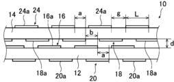
- the multilayer metasurface structure 10 shown in FIG. 1 includes a first substrate 12, a second substrate 14, a first structural layer 16, a second structural layer 18, a third structural layer 20, a fourth structural layer 24, and a spacer 26 disposed between the first substrate 12 and the second substrate 14.
- Figure 1 Figures 2 and 3 conceptually shows a cut of the multilayer metasurface structure cut in the thickness direction, i.e., the stacking direction of the first structure layer 16 to the fourth structure layer 24, and in the longitudinal direction of the first metal microstructure 16a to the fourth metal microstructure 24a described below, but in order to clearly show the configuration of the multilayer metasurface structure, hatching is omitted in all figures.
- the first structure layer 16 is formed using one surface (the top surface in the figure) of the first substrate 12, and is composed of a plurality of first metal microstructures 16a arranged (disposed) on the surface of the first substrate 12.
- the second structure layer 18 is formed using one surface (the bottom surface in the figure) of the second substrate 14, and is composed of a plurality of second metal microstructures 18a arranged (disposed) on the surface of the first substrate 12.
- the third structure layer 20 is formed using the other surface (the bottom surface in the figure) of the first substrate 12, and is composed of a plurality of third metal microstructures 20a arranged (disposed) on the surface of the first substrate 12.
- the fourth structure layer 24 is formed using the other surface (the top surface in the figure) of the second substrate 14, and is composed of a plurality of fourth metal microstructures 24a arranged (disposed) on the surface of the second substrate 14.
- the first substrate 12 and the first structure layer 16 constitute the first metasurface structure of the present invention.
- the second substrate 14 and the second structure layer 18 constitute the second metasurface structure of the present invention.
- the multilayer metasurface structure 10 shown in Figure 1 has a third metasurface structure composed of a first substrate 12 and a third structure layer 20, and a fourth metasurface structure composed of a second substrate 14 and a fourth structure layer 24.
- a metasurface refers to a structure in which a number of metal microstructures smaller than the optical wavelength corresponding to the design frequency, i.e., the frequency of the corresponding electromagnetic wave, are arranged on the surface of a dielectric film, and the macroscopic response to incident electromagnetic waves is utilized.
- the first substrate 12 and the second substrate 14 are stacked and fixed with the first structural layer 16 and the second structural layer 18 facing each other with a spacer 26 sandwiched between them.
- the multilayer metasurface structure 10 has the first substrate 12 and the second substrate 14 stacked with the spacer 26 sandwiched between them, thereby stacking the first structural layer 16 and the second structural layer 18 at a distance from each other.
- the first substrate 12 and the second substrate 14 are attached to each other by a spacer 26. This will be described in detail later.
- the first structural layer 16 and the third structural layer 20 are stacked while being spaced apart from each other by the first substrate 12, and the second structural layer 18 and the fourth structural layer 24 are stacked while being spaced apart from each other by the second substrate 14.
- the multilayer metasurface structure in the illustrated example has four layers, namely, a first structure layer 16 to a fourth structure layer 24.
- the multilayer metasurface structure of the invention may have only two structural layers as shown in FIG. 3, three structural layers, or even five or more structural layers, so long as it has a first structural layer 16 and a second structural layer 18.
- the following description also applies to multilayer metasurface structures having two to three, five or more structure layers.
- the multilayer metasurface structure 10 manufactured by the manufacturing method of the present invention is responsive to electromagnetic waves having a frequency of 10 THz or less, i.e., electromagnetic waves having a wavelength of 30 ⁇ m or more.
- the design electromagnetic wave of the multilayer metasurface structure 10 is preferably 10 THz or less.
- a multilayer metasurface structure that acts on electromagnetic waves with a frequency of 10 THz or less means that when electromagnetic waves of a certain frequency of 10 THz or less are incident on it, it functions as a body with a high refractive index against the electromagnetic waves, in other words, it functions as a structure that can obtain a high diffraction angle.
- the multilayer metasurface structure 10 acts on electromagnetic waves with a frequency of 10 GHz or more, i.e., a wavelength of 30 mm or less. More preferably, the multilayer metasurface structure 10 acts on electromagnetic waves with a frequency of 100 GHz or more, i.e., a wavelength of 3 mm or less. That is, it is preferable that the multilayer metasurface structure 10 is effective for electromagnetic waves having a frequency of 10 GHz to 10 THz, so-called terahertz waves (THz waves).
- THz waves terahertz waves
- the multilayer metasurface structure 10 is formed by stacking a first substrate 12 having a first structural layer 16 on one side and a third structural layer 20 on the other side, and a second substrate 14 having a second structural layer 18 on one side and a fourth structural layer 24 on the other side, with a spacer 26 interposed therebetween.
- the spacer 26 has a pattern (not a solid shape) that separates and stacks the first substrate 12 and the second substrate 14.
- the pattern shape preferably satisfies the following requirements.
- the spacer 26 may be a frame-shaped member that surrounds the arrangement of the first metal microstructures 16a of the first structure layer 16 and the arrangement of the second metal microstructures 18a of the second structure layer 18 in the in-plane direction of the first substrate 12 and the second substrate 14. When the spacer 26 is in the shape of a frame, a part of the frame may be cut out.
- the spacers 26 are provided in a region corresponding to 50% or more of the outer circumferential length of a frame body that surrounds the arrangement of the first metal microstructures 16a of the first structural layer 16 and the arrangement of the second metal microstructures 18a of the second structural layer 18 in the in-plane direction of the first substrate 12 and the second substrate 14, it is more preferable that the spacers 26 are provided in a region corresponding to 75% or more, and it is even more preferable that the spacers 26 are provided in a region corresponding to 90% or more.
- the first substrate 12 and the second substrate 14 are both substrates made of a dielectric material. That is, in the illustrated multilayer metasurface structure 10, the first substrate 12 acts as a dielectric layer provided between the first structural layer 16 and the third structural layer 20, and the second substrate 14 acts as a dielectric layer provided between the second structural layer 18 and the fourth structural layer 24.
- the spacer 26 also forms an air layer between the first structural layer 16 and the second structural layer 18, which acts as a dielectric layer.
- the multilayer metasurface structure 10 in the illustrated example is not limited to being formed by providing metal microstructures on both sides of a single substrate, and stacking two of these substrates at a distance from each other, with the first structure layer to the fourth structure layer stacked at a distance from each other.
- the multilayer metasurface structure may be formed by stacking four substrates, including a substrate having a first structure layer on one side, a substrate having a second structure layer on one side, a substrate having a third structure layer on one side, and a substrate having a fourth structure layer on one side, with the structure layers facing the substrates, so that the first to fourth structure layers are stacked at a distance from each other.
- first substrate 12 and the first structural layer 16 may be disposed between the first substrate 12 and the first structural layer 16, between the first substrate 12 and the third structural layer 20, between the second substrate 14 and the second structural layer 18, and between the second substrate 14 and the fourth structural layer 24.
- adhesive layers may be disposed between the first substrate 12 and the first structural layer 16, between the first substrate 12 and the third structural layer 20, between the second substrate 14 and the second structural layer 18, and between the second substrate 14 and the fourth structural layer 24.
- the first substrate 12 and the second substrate 14 are dielectric resin films.
- the dielectric resin film refers to one or more dielectric substrates that can be handled independently and on which a metal pattern can be formed.
- the dielectric substrate may have a single layer structure or a multilayer structure.
- dielectric substrates examples include polyesters such as polyethylene terephthalate (PET) and polyethylene naphthalate (PEN), polyethylene (PE), polypropylene (PP), polystyrene, ethylene vinyl acetate (EVA), polyolefins such as cycloolefin polymer (COP) and cycloolefin copolymer (COC), vinyl resins, polycarbonate (PC), polyamide, polyimide, acrylic resin, and dielectric substrates formed from triacetyl cellulose (TAC), etc.
- PET polyethylene terephthalate
- PEN polyethylene naphthalate
- PE polyethylene
- PP polypropylene
- EVA ethylene vinyl acetate
- polyolefins such as cycloolefin polymer (COP) and cycloolefin copolymer (COC)
- vinyl resins polycarbonate (PC)
- PC polyamide
- polyimide polyimide
- acrylic resin and dielectric substrates formed from
- the thickness of the first substrate 12 and the second substrate 14 is preferably 5 to 100 ⁇ m, more preferably 10 to 80 ⁇ m, and even more preferably 15 to 50 ⁇ m.
- the first substrate 12 and the second substrate 14 have a high transmittance for the electromagnetic waves to be transmitted.
- the transmittance for the electromagnetic waves to be transmitted through the first substrate 12 and the second substrate 14 is preferably 75% or more, more preferably 85% or more, and even more preferably 95% or more.
- the transmittance for the electromagnetic waves there is no particular upper limit to the transmittance for the electromagnetic waves, and it is often less than 100%.
- the first substrate 12 and the second substrate 14 have a thickness equal to or greater than a predetermined thickness, they are easy to handle.
- the first substrate 12 and the second substrate 14 have a thickness equal to or less than a predetermined value and/or have a transmittance equal to or greater than a predetermined value, they are more likely to function as a metamaterial.
- the materials forming the first substrate 12 and the second substrate 14 are usually the same, but may be different. Furthermore, the thicknesses of the first substrate 12 and the second substrate 14 are usually the same, but may be different.
- the multilayer metasurface structure 10 is formed by stacking a first substrate 12 and a second substrate 14 with a spacer 26 interposed therebetween.
- the spacers 26 are formed in a pattern.
- the spacers 26 are in the form of frames that surround the array of first metal microstructures 16a of the first structure layer 16 and the array of second metal microstructures 18a of the second structure layer 18 in the in-plane direction of the first substrate 12 and the second substrate 14.
- the spacer 26 is not limited to having a frame-shaped pattern surrounding the arrangement of the first metal microstructures 16a and the second metal microstructures 18a, and various patterns can be used depending on the arrangement of the metal microstructures.
- examples include a pattern consisting of a rectangular frame body and a diagonal line of the frame body, a pattern consisting of a circular frame body and a line crossing the circle in the diameter direction, and a pattern consisting of a rectangular frame body and a line parallel to the frame body.
- the spacer 26 having a frame-shaped pattern surrounding the arrangement of the first metal microstructures 16a and the second metal microstructures 18a is preferably used.
- the thickness of the spacer 26 there is no restriction on the distance between the first substrate 12 and the second substrate 14, i.e., the thickness of the spacer 26, and the distance may be set appropriately so as to ensure an air layer of sufficient thickness to act as a dielectric layer.
- the distance may be set appropriately so as to ensure an air layer of sufficient thickness to act as a dielectric layer.
- the thickness of the spacer 26 is sufficiently thinner than the wavelength of the electromagnetic wave of interest, the proximity (bonding) of the first metal microstructure 16a and the second metal microstructure 18a may change the resonance structure and deform the resonance peak, but this effect can be actively utilized.
- care must be taken not to affect the transmitted electromagnetic wave due to alignment errors, etc., that occur during stacking.
- the thickness of the spacer 26 can be made sufficiently large so that resonance between the first metal microstructure 16a and the second metal microstructure 18a can be ignored and so that alignment errors occurring during stacking do not affect the electromagnetic waves passing through.
- the spacer 26 contains at least a polymer (cured product) of a polymerizable compound.
- the first structure layer 16 is formed by arranging a plurality of first metal microstructures 16a at a distance from one another on one surface (the upper surface in the figure) of the first substrate 12.
- the first structure layer 16 is basically composed of an arrangement of unit cells each formed by one first metal microstructure 16a and the space surrounding the first metal microstructure 16a.
- the second structure layer 18 is formed by arranging a plurality of second metal microstructures 18a at a distance from one another on one surface (the lower surface in the figure) of the second substrate 14.
- the second structure layer 18 is basically constituted by an arrangement of unit cells each formed by one second metal microstructure 18a and the space surrounding the second metal microstructure 18a.
- the third structure layer 20 is formed by arranging a plurality of third metal microstructures 20a at a distance from one another on the other surface (the lower surface in the figure) of the first substrate 12.
- the third structure layer 20 is basically constituted by an arrangement of unit cells each formed by one third metal microstructure 20a and the space surrounding the third metal microstructure 20a.
- the fourth structure layer 24 is formed by arranging a plurality of fourth metal microstructures 24a at a distance from one another on the other surface (the lower surface in the figure) of the second substrate 14.
- the fourth structure layer 24 is basically constituted by an arrangement of unit cells each formed by one fourth metal microstructure 24a and the space surrounding the fourth metal microstructure 24a.
- the first structure layer 16 to the fourth structure layer 24 all use the surface of a corresponding substrate, and have the same basic structure in which the first metal microstructure 16a to the fourth metal microstructure 24a are arranged on this surface. Therefore, in the following description, when there is no need to distinguish between the first structure layer 16 to the fourth structure layer 24, they will also be collectively referred to as structure layers. Similarly, when there is no need to distinguish between the first metal microstructure 16a to the fourth metal microstructure 24a, they will also be collectively referred to as metal microstructures.
- the structure layer has a configuration similar to that of a conventional metasurface structure (metamaterial), in which metal microstructures (unit cells) are arranged on one surface of a substrate. Therefore, there are no limitations on the shape of the metal microstructures, the arrangement of the metal microstructures, the spacing (pitch) of the metal microstructures, and the like.
- the metal microstructures are made of metal. As described above, the multilayer metasurface structure 10 is preferably adapted to act on electromagnetic waves with frequencies of 10 THz or less. Metals have high electrical conductivity and transmittance for electromagnetic waves with frequencies of 10 THz or less. Therefore, by using metal microstructures, the multilayer metasurface structure 10 can efficiently refract electromagnetic waves with frequencies of 10 THz or less.
- the material for forming the metal microstructure is not particularly limited as long as it contains a metal in part and causes resonance when a specific electromagnetic wave is incident thereon, and the metal microstructure may contain, in addition to metal, a dielectric material, a magnetic material, etc. Furthermore, the metal microstructure may contain, in part, a conductive material such as a conductive polymer. Preferred examples of the metal include gold, silver, platinum, copper, aluminum, and alloys containing one or more of these, with silver and copper being more preferred.
- the metal microstructures that make up the structure layer, and various shapes used as metal microstructures (resonators) in known metasurface structures can be used. It is preferable that the metal microstructure has a structure and properties in which, when electromagnetic waves are incident, electric resonance and magnetic resonance occur simultaneously due to interaction between the electric field and magnetic field of the incident electromagnetic waves, and the effective dielectric constant and permeability can be controlled simultaneously.
- Examples of the shape of the metal microstructure include a metal cut wire, a cross or swastika shape formed by crossing metal cut wires, a C shape, a U shape, a double ring shape, a V shape, an L shape, an H shape, a lattice shape, a spiral shape, a square shape, and a circle shape.
- a solid body having a bottom shape as shown in Figure 5 of "Appl. Sci. 2018, 8(9), 1689; https://doi.org/10.3390/app8091689" can also be used.
- a metal cut wire (a metal rod) is preferably used.
- the cross-sectional shape of the metal cut wire there is no limitation on the cross-sectional shape of the metal cut wire, and various columnar shapes such as a quadrangular prism, a triangular prism, and a cylindrical shape can be used.
- the quadrangular prism the cross section in the direction perpendicular to the longitudinal direction can have various shapes such as a square, a rectangle, a parallelogram, and a trapezoid.
- triangular prism various shapes such as an equilateral triangle and an isosceles triangle can be used, and in the cylinder, not only a circle but also an ellipse can be used.
- metal microstructure In one structure layer, only one type of metal microstructure may be used, or a plurality of types may be used in combination. Furthermore, the metal microstructures in each structure layer may be the same or different.
- the size of the metal microstructures there is no limit to the size of the metal microstructures, but as with conventional metasurface structures (metamaterials), the size should be less than the wavelength of the target electromagnetic wave, preferably less than 1.0 times the wavelength, and more preferably less than 0.5 times the wavelength.
- the size (major axis) of the metal microstructure is preferably 1 to 3000 ⁇ m, and more preferably 5 to 1000 ⁇ m.
- the multilayer metasurface structure 10 shown in Figure 1 has a first metal microstructure 16a, a second metal microstructure 18a, a third metal microstructure 20a, and a fourth metal microstructure 24a that are arranged offset from each other in the in-plane direction of the first substrate 12 and the second substrate 14.
- first metal microstructure 16a, the second metal microstructure 18a, the third metal microstructure 20a, and the fourth metal microstructure 24a do not completely overlap.
- the normal direction is a direction perpendicular to the main surface of the sheet-like material, and in the multilayer metasurface structure 10, it is the thickness direction, i.e., the stacking direction of the structure layers, i.e., the stacking direction of the first substrate 12, the spacer 26 and the second substrate 14.
- the main surface is the largest surface of the sheet-like material, and usually both surfaces in the thickness direction.
- the multilayer metasurface structure manufactured by the manufacturing method of the present invention is not limited to this, and as conceptually shown in Figure 2, the first metal microstructure 16a, the second metal microstructure 18a, the third metal microstructure 20a, and the fourth metal microstructure 24a may be arranged in line with each other in the in-plane direction of the first substrate 12 and the second substrate 14. That is, when viewed from the normal direction of the substrate, the multilayer metasurface structure may have the first metal microstructure 16a, the second metal microstructure 18a, the third metal microstructure 20a, and the fourth metal microstructure 24a completely overlapping.
- the multilayer metasurface structure manufactured by the manufacturing method of the present invention may have only two structural layers, a first structural layer 16 and a second structural layer 18, as conceptually shown in Figure 3.
- the multilayer metasurface structure manufactured by the manufacturing method of the present invention may focus, diffuse, or refract electromagnetic waves in one direction.
- the multilayer metasurface structure may be of either a transmission type or a reflection type, but is preferably of a transmission type. Therefore, the multilayer metasurface structure can be used in a variety of known elements, such as metalenses such as convex and concave lenses, and deflection elements that bend electromagnetic waves.
- the multilayer metasurface structure can be made into a sheet-type element by providing a refractive index distribution structure in the structure layer by utilizing the characteristic optical response exhibited by the metal microstructure in the structure layer. Therefore, the multilayer metasurface structure is preferably a sheet-type metalens such as a convex lens or a concave lens.
- the multilayer metasurface structure of the present invention is a multilayer metasurface structure manufactured by the manufacturing method of the present invention having steps 1 to 3 shown below.
- a first metasurface structure is prepared in which a first structure layer 16 having first metal microstructures 16a arranged thereon is provided on one surface of a first substrate 12.
- a third metasurface structure is provided in which a third structure layer 20 having third metal microstructures 20a arranged thereon is provided on the other surface of the first substrate 12.
- a second metasurface structure is prepared in which a second structure layer 18 having second metal microstructures 18a arranged thereon is provided on one surface of a second substrate 14.
- a fourth metasurface structure is provided in which a fourth structure layer 24 having fourth metal microstructures 24a arranged thereon is provided on the other surface of the second substrate 14.
- the way in which the multilayer metasurface structure reacts to electromagnetic waves with frequencies of 10 THz or less can be set by appropriately selecting and combining the shape and material of the metal microstructures in each structure layer, the arrangement of the metal microstructures, and the spacing between the metal microstructures, etc.
- the metal microstructures used and the arrangement of the metal microstructures in each structure layer may be set using known methods so as to obtain the desired characteristics of the multilayer metasurface structure.
- the metasurface structure is a sheet-type lens (convex lens)
- the arrangement density of the metal microstructures is gradually decreased from the center toward the periphery so that the phase difference imparted to the transmitted electromagnetic wave gradually decreases from the center toward the periphery.
- the amplitude and phase of the electromagnetic waves passing through the metal microstructures to be used can be calculated using commercially available simulation software, and the arrangement of the metal microstructures can be set so as to achieve the desired distribution of phase difference (phase modulation amount (refractive index)).
- a metal layer may be formed on both sides (or one side) of a substrate by a known film formation method such as sputtering, and a structural layer may be formed on this metal layer by arranging metal microstructures using photolithography technology.
- step 1 in the manufacturing method of the multilayer metasurface structure of the present invention, first, in step 1, as conceptually shown in the middle part of Figure 4, spacer portions 26a which become frame-shaped spacers 26 are formed in a pattern on the first metasurface structure (i.e., the surface of the first substrate 12 on which the first structure layer 16 is formed) so as to surround the arrangement of first metal microstructures 16a which constitute the first structure layer 16 in the substrate surface direction.
- step 2 as conceptually shown in the lower part of Figure 4, the spacer portion 26a and the second metasurface structure, i.e., the surface on which the second structure layer 18 of the second substrate 14 is formed, are bonded to obtain a laminate including the first metasurface structure, the spacer portion 26a and the second metasurface structure.
- the spacer portion 26a contains a polymerizable compound and has some adhesiveness until it is polymerized in the subsequent step 3. Therefore, even after the spacer portion 26a and the second metasurface structure (i.e., the surface on which the second structure layer 18 of the second substrate 14 is formed) are laminated and bonded together in step 2, they can be easily peeled off and rebonded. Moreover, in the manufacturing method of the present invention, since the spacer portion 26a is arranged in a pattern, the first metasurface structure and the second metasurface structure are not entirely bonded together. In the illustrated example, as a preferred embodiment, the spacer portion 26a has a frame-shaped pattern.
- step 3 described later the polymerizable compound in the spacer portion 26a is polymerized, and the adhesion between the first metasurface structure and the second metasurface structure is improved.
- the manufacturing method of the layered metasurface structure of the present invention thereby makes it possible to manufacture a layered metasurface structure with high positional accuracy between the metasurface structures.
- a multilayer metasurface structure which is made by stacking multiple metasurface structures, is capable of imparting a larger phase to an incident electromagnetic wave than a conventional single-layer metasurface structure.
- the microstructures forming the metasurface structure are very small. For example, in the case of electromagnetic waves with a frequency of 0.1 to 10 THz as described above, the size of the microstructure is exemplified as 1 to 3000 ⁇ m. Therefore, in order to stack the metasurface structures in the appropriate positional relationship, extremely high precision is required, and it is rare that the metasurface structures can be stacked in the appropriate positional relationship in a single operation.
- the stacked metasurface structures are attached with an adhesive, so that even if the positional relationship between the stacked metasurface structures is not correct, it is very difficult to peel off the stacked metasurface structures.
- the second metasurface structure can be easily peeled off even after the spacer portion 26a and the second metasurface structure are stacked to form a laminate including the first metasurface structure, the spacer portion 26a and the second metasurface structure. Therefore, even if the positional relationship between the first metasurface structure and the second metasurface structure is inappropriate when the spacer portion 26a and the second metasurface structure are stacked, the second metasurface structure can be easily peeled off, realigned, and the spacer portion 26a and the second metasurface structure can be stacked. As a result, according to the manufacturing method of the present invention, it is possible to suitably align metasurface structures with each other, and it is possible to manufacture a multilayer metasurface structure having excellent positional accuracy between the metasurface structures.
- Step 1 of the manufacturing method of the present invention is a step of arranging a spacer portion containing a polymerizable compound in a pattern on a first metasurface structure including a first substrate and a first structure layer provided on at least one surface side of the first substrate, the first structure layer having a plurality of first metal microstructures arranged in the in-plane direction.
- the first metasurface structure including the first structure layer used in this process is as described above.
- the spacer portion used in this process contains a polymerizable compound. As described above, the spacer portion contains a polymerizable compound, which causes some adhesion. Furthermore, during the polymerization process in step 3 described below, polymerization of the polymerizable compound progresses, improving the adhesion between the first metasurface structure and the second metasurface structure.
- the type of polymerizable compound contained in the spacer portion is not particularly limited, and any known polymerizable compound can be used.
- the polymerizable compound means a compound different from the resin described below.
- the polymerizable group of the polymerizable compound may be any group that is involved in a polymerization reaction, and examples thereof include groups having an ethylenically unsaturated group such as a vinyl group, an acryloyl group, a methacryloyl group, a styryl group, and a maleimide group; and groups having a cationic polymerizable group such as an epoxy group and an oxetane group.
- a group having an ethylenically unsaturated group is preferable, and an acryloyl group or a methacryloyl group is more preferable.
- the polymerizable compound a compound having one or more ethylenically unsaturated groups is preferable, and a compound having two or more ethylenically unsaturated groups in the molecule is more preferable.
- the number of ethylenically unsaturated groups in the molecule of the ethylenically unsaturated compound is preferably 1 to 6, more preferably 1 to 3, even more preferably 2 or 3, and particularly preferably 3.
- the polymerizable compound may have an alkyleneoxy group.
- the alkyleneoxy group is preferably an ethyleneoxy group or a propyleneoxy group, and more preferably an ethyleneoxy group in terms of superior effects of the present invention.
- the number of alkyleneoxy groups in the polymerizable compound is preferably 2 to 30, more preferably 2 to 20, per molecule.
- the polymerizable compound contains a polymerizable compound X.
- the polymerizable compound X is a bifunctional ethylenically unsaturated compound having one or more aromatic rings in the molecule, among the above polymerizable compounds.
- aromatic ring of the polymerizable compound X examples include aromatic hydrocarbon rings such as a benzene ring, a naphthalene ring, and an anthracene ring; aromatic heterocycles such as a thiophene ring, a furan ring, a pyrrole ring, an imidazole ring, a triazole ring, and a pyridine ring; and condensed rings thereof, with an aromatic hydrocarbon ring being preferred, and a benzene ring being more preferred.
- the aromatic ring may have a substituent.
- the polymerizable compound X may have two or more aromatic rings.
- the polymerizable compound X preferably has a bisphenol structure, since this suppresses swelling of the photosensitive layer due to a developer, thereby improving the resolution.
- the bisphenol structure include a bisphenol A structure derived from bisphenol A (2,2-bis(4-hydroxyphenyl)propane), a bisphenol F structure derived from bisphenol F (2,2-bis(4-hydroxyphenyl)methane), and a bisphenol B structure derived from bisphenol B (2,2-bis(4-hydroxyphenyl)butane), with the bisphenol A structure being preferred.
- An example of the polymerizable compound X having a bisphenol structure is a compound having a bisphenol structure and two polymerizable groups (preferably (meth)acryloyl groups) bonded to both ends of the bisphenol structure. Both ends of the bisphenol structure may be directly bonded to the two polymerizable groups, or may be bonded via one or more alkyleneoxy groups.
- the alkyleneoxy groups added to both ends of the bisphenol structure are preferably ethyleneoxy groups or propyleneoxy groups, and more preferably ethyleneoxy groups.
- the number of alkyleneoxy groups (preferably ethyleneoxy groups) added to the bisphenol structure is preferably 2 to 30, and more preferably 2 to 20, per molecule.
- the polymerizable compound also includes difunctional ethylenically unsaturated compounds having no aromatic ring and tri- or higher functional ethylenically unsaturated compounds.
- difunctional ethylenically unsaturated compounds having no aromatic ring include alkylene glycol di(meth)acrylates, polyalkylene glycol di(meth)acrylates, urethane di(meth)acrylates, and trimethylolpropane diacrylate.
- the molecular weight of the polymerizable compound is preferably 200 to 3,000, more preferably 280 to 2,200, and even more preferably 300 to 2,200.
- the content of the polymerizable group in the polymerizable compound is preferably 1.0 mmol/g or more, more preferably 2.0 mmol/g or more, and the upper limit is preferably 10.0 mmol/g or less.
- the spacer portion contains a plurality of polymerizable compounds
- the content of the polymerizable groups in all of the contained polymerizable compounds is preferably within the above-mentioned preferred embodiment.
- the "content of polymerizable group” means the equivalent (mol) of the polymerizable group contained per gram of the polymerizable compound.
- the polymerizable compounds may be used alone or in combination of two or more.
- the content of the polymerizable compound is preferably from 5 to 70% by mass, and more preferably from 10 to 60% by mass, based on the total mass of the spacer portion.
- the spacer portion may contain components other than the polymerizable compound.
- the other components include resins.
- the resin is preferably a (meth)acrylic resin.
- the (meth)acrylic resin is a resin having a structural unit derived from a (meth)acrylic compound, and examples of the (meth)acrylic compound include (meth)acrylic acid, (meth)acrylic acid esters, (meth)acrylamide, and (meth)acrylonitrile, etc.
- the content of the structural unit derived from the (meth)acrylic compound is preferably 50% by mass or more, more preferably 70% by mass or more, and even more preferably 90% by mass or more, based on the total structural units of the resin.
- the (meth)acrylic resin preferably contains, for example, a structural unit having an aromatic ring structure (for example, a structural unit derived from styrene and a structural unit derived from benzyl (meth)acrylate, etc.), a structural unit having an aliphatic hydrocarbon ring structure (for example, a structural unit having an aliphatic hydrocarbon ring structure such as a tricyclodecane ring, a cyclohexane ring, a cyclopentane ring, a norbornane ring, an isoborone ring, or a tetrahydrodicyclopentadiene ring), a structural unit having an acid group (examples of the acid group include a carboxy group, a sulfo group, a phosphonic acid group, and a phosphoric acid group), and a structural unit having a reactive group (for example, a polymerizable group).
- an aromatic ring structure for example,
- the content of the structural unit having an aromatic ring structure is preferably 10 to 90 mass%, and more preferably 20 to 80 mass%, based on the total structural units of the (meth)acrylic resin.
- the content of the structural unit having an acid group is preferably 5 to 50 mass%, and more preferably 5 to 40 mass%, based on the total structural units of the (meth)acrylic resin.
- the content of the structural unit having a reactive group is preferably 5 to 70 mass%, and more preferably 10 to 50 mass%, based on the total structural units of the (meth)acrylic resin.
- the weight average molecular weight of the resin is preferably from 5,000 to 500,000, more preferably from 10,000 to 100,000, and even more preferably from 10,000 to 60,000.
- the Tg of the resin is preferably from 60 to 135°C, and more preferably from 70 to 120°C.
- the resins may be used alone or in combination of two or more.
- the resin content is preferably from 10 to 85% by mass, and more preferably from 20 to 75% by mass, based on the total mass of the spacer portion.
- the spacer portion may contain other components such as a surfactant, a polymerization initiator, a sensitizer, a color developer, and a rust inhibitor.
- the thickness of the spacer portion is preferably 1 to 5000 ⁇ m, and more preferably 10 to 1000 ⁇ m.
- the spacer portions are arranged in a pattern.
- the shape of the pattern is not particularly limited, and they are arranged so as to form the spacer pattern described above. For example, as described above, they are arranged so as to obtain a spacer having a frame-shaped pattern that surrounds the arrangement of the first metal microstructures and the second metal microstructures.
- frame-shaped spacer portions may be arranged on the first metasurface structure so as to surround the arrangement of the first metal microstructures.
- the melt viscosity of the spacer portion is not particularly limited, it is preferable that the melt viscosity at 23° C. is 1.0 ⁇ 10 5 Pa ⁇ s or more and the melt viscosity at 80° C. is less than 1.0 ⁇ 10 5 Pa ⁇ s.
- the melt viscosity of the spacer portion satisfies the above characteristics, the second metasurface structure can be more easily peeled off after being bonded to the spacer portion, improving the productivity of the multilayer metasurface structure.
- the melt viscosity of the spacer portion at 23° C. is preferably 1.0 ⁇ 10 10 Pa ⁇ s or less.
- the melt viscosity of the spacer portion at 80° C. is preferably 1.0 ⁇ 10 1 Pa ⁇ s or more.
- the melt viscosity ⁇ c of the spacer portion at 23° C. and 80° C. is measured as follows. After preparing a spacer portion having a thickness of about 0.5 mm, the melt viscosity is measured using a rheometer DHR-2 manufactured by T.A. Instruments (using a 20 mm ⁇ parallel plate and a Peltier plate (Gap: about 0.5 mm)) at a set temperature of 20-125° C., a heating rate of 5° C./min, a frequency of 1 Hz, and a strain of 0.5%, and the melt viscosity at each temperature is calculated from the measured values at 23° C. and 80° C.
- step 1 includes step A of forming a photosensitive layer containing a polymerizable compound on a first metasurface structure including a first structure layer having a first substrate and a plurality of first metal microstructures arranged in the in-plane direction on the first substrate, step B of exposing the photosensitive layer to light in a pattern, and step C of developing the exposed photosensitive layer to form a spacer portion.
- steps A to C a photosensitive layer is formed on the first metasurface structure, and then unnecessary portions are removed to form a patterned spacer portion. Steps A to C will be described in detail below.
- the method of forming the photosensitive layer is not particularly limited as long as it is possible to form a photosensitive layer containing a polymerizable compound on the first metasurface structure, but examples include a method using a transfer film and a method of applying a photosensitive composition.
- a method using a transfer film a method is preferred in which a transfer film containing a temporary support and a photosensitive layer is prepared, and the transfer film is attached to the first metasurface structure so that the photosensitive layer side of the transfer film faces the first structure layer.
- a method of applying a photosensitive composition a method is used in which a photosensitive composition is applied onto the first structure layer of the first metasurface structure to form a photosensitive layer.
- the method using a transfer film is preferred.
- the temporary support included in the transfer film is preferably a film, more preferably a resin film, such as a polyethylene terephthalate film (e.g., a biaxially stretched polyethylene terephthalate film), a polymethyl methacrylate film, a cellulose triacetate film, a polystyrene film, a polyimide film, or a polycarbonate film.
- the thickness of the temporary support is preferably 5 ⁇ m or more, more preferably 6 ⁇ m or more.
- the upper limit is preferably 200 ⁇ m or less, and from the viewpoint of ease of handling and versatility, more preferably 150 ⁇ m or less, even more preferably 50 ⁇ m or less.
- the surface of the temporary support which comes into contact with the photosensitive layer may be subjected to a surface modification treatment.
- surface modification treatments include treatments using UV irradiation, corona discharge, plasma, and the like.
- the photosensitive layer preferably contains the above-mentioned polymerizable compound, and more preferably contains the above-mentioned polymerizable compound and resin.
- the content of the polymerizable compound is preferably from 5 to 70% by mass, and more preferably from 15 to 60% by mass, based on the total mass of the photosensitive layer.
- the content of the resin is preferably from 10 to 85% by mass, and more preferably from 20 to 75% by mass, based on the total mass of the photosensitive layer.
- the photosensitive layer may contain components other than the polymerizable compound and the resin.
- the other components include a polymerization initiator.
- a polymerization initiator known polymerization initiators can be used depending on the type of polymerization reaction.
- the polymerization initiator may be either a radical polymerization initiator or a cationic polymerization initiator, with a radical polymerization initiator being preferred.
- the radical polymerization initiator examples include a polymerization initiator having an oxime ester structure, a polymerization initiator having an ⁇ -aminoalkylphenone structure, a polymerization initiator having an ⁇ -hydroxyalkylphenone structure, a polymerization initiator having an acylphosphine oxide structure, and a polymerization initiator having an N-phenylglycine structure.
- the radical polymerization initiator preferably contains at least one selected from the group consisting of 2,4,5-triarylimidazole dimers and derivatives thereof.
- the content of the polymerization initiator is preferably from 0.1 to 20% by mass, and more preferably from 0.5 to 10% by mass, based on the total mass of the photosensitive layer.
- the photosensitive layer may contain polymerization inhibitors, surfactants, sensitizers, color formers, rust inhibitors, etc.
- the method for attaching the transfer film to the first metasurface structure is not particularly limited, but a method of thermocompression using a roll or the like is preferred.
- step B is carried out in which the photosensitive layer is exposed to light in a pattern.
- the exposed portions of the photosensitive layer remain as spacer portions as described below. It is preferable to set the exposure conditions so that a portion of the polymerizable compound contained in the photosensitive layer remains after exposure.
- the exposure method may be a known method, for example, a method using a photomask. By disposing a photomask between the photosensitive layer and the exposure light source, the photosensitive layer can be exposed to pattern light through the photomask.
- exposure light sources include various lasers, light-emitting diodes (LEDs), ultra-high pressure mercury lamps, high pressure mercury lamps, and metal halide lamps.
- the exposure dose is preferably 5 to 200 mJ/ cm2 , more preferably 10 to 200 mJ/ cm2 .
- the exposure dose is determined by the illuminance of the light source and the exposure time.
- the exposure dose may be measured using a known actinometer.
- the photosensitive layer may be exposed by using a direct imaging device without using a photomask.
- the exposed photosensitive layer is subjected to a development treatment to form spacer portions in step C.
- a development treatment to form spacer portions in step C.
- the development process may be carried out by a known method using a developer, such as paddle development, shower development, spin development, or dip development.
- the developer is preferably an alkaline aqueous solution.
- alkaline compound contained in the alkaline aqueous solution include sodium hydroxide, potassium hydroxide, sodium carbonate, and sodium hydrogen carbonate.
- step 1 is a step in which step 1 is a step of forming a spacer portion by laminating a photosensitive layer containing a patterned polymerizable compound on a first metasurface structure including a first substrate and a first structure layer having a plurality of first metal microstructures arranged in the in-plane direction on the first substrate.
- a patterned photosensitive layer containing a polymerizable compound is laminated directly on the first metasurface structure. This patterned photosensitive layer corresponds to the spacer portion.
- a method using a transfer film including a temporary support and a photosensitive layer including a pattern-shaped polymerizable compound arranged on the temporary support is preferred.
- a method of preparing a transfer film including a temporary support and a photosensitive layer including a pattern-shaped polymerizable compound, and attaching the transfer film to the first metasurface structure so that the photosensitive layer side of the transfer film faces the first structure layer can be mentioned.
- the structures of the temporary support and the photosensitive layer constituting the transfer film are as described above.
- the method for forming the pattern-shaped photosensitive layer containing a polymerizable compound is not particularly limited, and examples thereof include a method in which unnecessary portions of the photosensitive layer in a transfer film are cut out.
- the method for attaching the transfer film to the first metasurface structure is not particularly limited, but a method of thermocompression bonding using a roll or the like is preferable.
- a step 2 is carried out in which a second metasurface structure including a second substrate and a second structure layer having a plurality of second metal microstructures arranged in the in-plane direction and provided on at least one surface side of the second substrate is bonded to a spacer portion to obtain a laminate including the first metasurface structure, the spacer portion, and the second metasurface structure.
- the method for bonding the spacer portion and the second metasurface structure is not particularly limited, and any known method can be used.
- the second metasurface structure can be easily peeled off, so that the second metasurface structure can be stacked on the spacer portion with high positional accuracy.
- step 3 is carried out to polymerize the polymerizable compound. That is, step 3 is a step of hardening the polymerizable compound.
- step 3 is a step of hardening the polymerizable compound.
- polymerization of the polymerizable compound in the spacer portion progresses, and the adhesion between the first metasurface structure and the second metasurface structure is improved.
- the spacer 26 described in FIG. 1 is formed.
- the method for polymerizing the polymerizable compound is not particularly limited, and examples thereof include heat treatment and light irradiation treatment, with heat treatment being preferred from the viewpoint of polymerizability.
- the conditions for the heat treatment are not particularly limited, and the optimum conditions are selected depending on the type of polymerizable compound used.
- the heating temperature during the heat treatment is preferably 80 to 250° C., more preferably 90 to 160° C.
- the heating time during the heat treatment is preferably 1 to 180 minutes, more preferably 5 to 60 minutes.
- the laminate Before or simultaneously with the heat treatment, the laminate may be subjected to an exposure treatment (hereinafter also referred to as a post-exposure treatment) as necessary.
- exposure light sources in the post-exposure treatment include various lasers, light-emitting diodes (LEDs), ultra-high pressure mercury lamps, high pressure mercury lamps, and metal halide lamps.
- the exposure dose in the post-exposure treatment is preferably from 100 to 5000 mJ/cm 2 , and more preferably from 200 to 3000 mJ/cm 2 .
- reaction solution was then reacted for another 3 hours.
- the reaction solution was diluted with propylene glycol monomethyl ether acetate (33 g) and propylene glycol monomethyl ether (100 g). Under an air stream, the diluted reaction solution was heated to 100° C., and tetraethylammonium bromide (0.53 g) and p-methoxyphenol (0.26 g) were added.
- glycidyl methacrylate (Blenmer G manufactured by NOF Corp.) (32 g) was added dropwise over 20 minutes. The resulting reaction solution was reacted at 100° C.
- Table 1 shows the amount of structural units, weight average molecular weight, double bond content, and glass transition temperature (Tg) of each of the synthesized resins.
- Tg glass transition temperature
- st styrene MMA: structural unit derived from methyl methacrylate
- MAA structural unit derived from methacrylic acid
- GMA-MAA structural unit obtained by adding glycidyl methacrylate to a structural unit derived from methacrylic acid
- BzMA structural unit derived from benzyl methacrylate
- compositions 1 to 3 were prepared according to the formulations shown in Table 2.
- the numerical values of each component shown in Table 2 represent parts by mass.
- the abbreviations shown in Table 2 are as follows.
- BPE-100 ethoxylated bisphenol A dimethacrylate, manufactured by Shin-Nakamura Chemical Co., Ltd.
- M-270 Aronix M-270, polypropylene glycol diacrylate (n ⁇ 12), manufactured by Toagosei Co., Ltd.
- BPE-500 ethoxylated bisphenol A dimethacrylate, manufactured by Shin-Nakamura Chemical Co., Ltd. (double bond content: 2.49 mmol/g)
- Phenothiazine/Phenidone Phenidone 1% solution in methyl ethyl ketone (MEK)
- (anti-rust) CBT-1 Carboxybenzotriazole, manufactured by Johoku Chemical Co., Ltd.
- a transfer film was prepared using the above composition.
- the specific steps are as follows: First, the composition 1 was applied to the surface of a temporary support (a polyethylene terephthalate film (E5001, manufactured by Toyobo Co., Ltd.) having a thickness of 100 ⁇ m) using a bar coater so as to form a coating film having a thickness of about 20 ⁇ m after drying. Next, the coating film was dried at 90° C. using an oven. This operation was repeated five times to form a film so as to form a photosensitive layer with a total thickness of 100 ⁇ m, and then a polypropylene film (E-201F, manufactured by Oji F-Tex Co., Ltd.) was attached as a protective film to prepare transfer film 1.
- a temporary support a polyethylene terephthalate film (E5001, manufactured by Toyobo Co., Ltd.) having a thickness of 100 ⁇ m
- E5001 polyethylene terephthalate film
- a bar coater so as to form
- Transfer film 2 was prepared according to the same procedure as above, except that composition 2 was used instead of composition 1. Further, a transfer film 3 was prepared in the same manner as above, except that the composition 1 was changed to the composition 3 and the total thickness of the photosensitive layer was set to 20 ⁇ m. Further, a transfer film 4 was prepared in the same manner as above, except that the composition 1 was changed to the composition 4 and the total thickness of the photosensitive layer was set to 20 ⁇ m.
- a cycloolefin polymer film (COP film) (thickness: 40 ⁇ m) was prepared as the first substrate and the second substrate.
- the first substrate was cut into a size of 10 x 10 cm, and the surface was ultrasonically cleaned (45 kHz).
- the cut first substrate was then placed inside a sputtering device. After reducing the pressure inside the device, argon gas was introduced, and sputtering was performed using copper as a target.
- the sputtering conditions were Ar gas pressure: 2 mTorr (0.27 Pa), and power supply: 3.3 W/ cm2 . This sputtering was carried out on each side of the first substrate in turn, forming copper layers with a thickness of 100 nm on both sides of the first substrate.
- composition for forming a negative resist layer was applied onto a temporary support (PET film, average thickness 30 ⁇ m, haze 0.19%) using a slit nozzle so as to give a dry film thickness of 3 ⁇ m and a coating width of 1 m.
- a temporary support PET film, average thickness 30 ⁇ m, haze 0.19%
- composition 1B for forming a negative resist layer described in paragraph 0562 of JP-A-2020-204757 was used as the composition for forming a negative resist layer described in paragraph 0562 of JP-A-2020-204757.
- the temporary support coated with the composition for forming a negative resist layer was passed through a drying zone at 80°C for 40 seconds, and then a protective film (polyethylene film, manufactured by Tredegar, OSM-N) was pressed onto the temporary support to prepare a negative transfer material.
- the prepared negative transfer material had a temporary support, a negative resist layer, and a protective film in this order.
- the prepared negative transfer material was cut into a size of 9 ⁇ 9 cm, and the protective film was peeled off from the negative transfer material.
- the first substrate and the negative transfer material were bonded together so that the negative resist layer surface exposed by peeling off the protective film was in contact with the copper layer.
- the negative transfer material was bonded to both sides of the first substrate in order, one side at a time, to obtain a laminate. This bonding was performed under the conditions of a roll temperature of 100° C., a linear pressure of 1.0 MPa, and a linear speed of 4.0 m/min.
- a photomask having a pattern complementary to the metal microstructure was laminated on the temporary support side of the negative transfer material on both sides of the obtained laminate.
- an ultra-high pressure mercury lamp manufactured by Dai Nippon Kaken Co., Ltd., MAP-1200L, exposure dominant wavelength: 365 nm
- the photomask pattern was formed only in a central region of 1 ⁇ 1 cm within the substrate surface.
- the patterns were different on both sides of the first substrate, with one side having a design corresponding to the pattern of the first structure layer described below, and the other side having a design corresponding to the pattern of the third structure layer described below.
- the temporary supports of the negative transfer materials on both sides were peeled off from the exposed laminate.
- the laminate was subjected to shower development for 30 seconds using a 1.0% aqueous sodium carbonate solution at a liquid temperature of 25° C., thereby forming resist patterns on the copper layers on both sides.
- the copper layer of the obtained laminate was etched using a copper etching solution (Cu-02, manufactured by Kanto Chemical Co., Ltd.) at 23° C. for 30 seconds.
- the resist pattern was stripped using propylene glycol monomethyl ether acetate.
- a first structure layer (first metasurface structure) was formed in a 1 x 1 cm area in the center of one surface of the first substrate, in which first metal microstructures (metal cut wires) having a length L of 0.4 mm and a width W of 0.05 mm were arranged in a lattice pattern with a longitudinal spacing g of 0.02 mm and a lateral spacing y of 0.09 mm, as conceptually shown in Figures 5 and 6 .
- a third structure layer (third metasurface structure) in which third metal microstructures were similarly arranged was formed on the other surface of the first substrate, with the third structure layer being formed such that the longitudinal deviation a between the first metal microstructures and the third metal microstructures was 0.28 mm.
- a second structure layer (second metasurface structure) and a fourth structure layer (fourth metasurface structure) were formed on the second substrate in exactly the same manner as the first structure layer and the third structure layer.
- the photosensitive layer exposed by peeling off the temporary support of the transfer film 1 of the obtained laminate was bonded to one side (the side on the second structure layer side) of a second substrate (COP film) on both sides of which another metal microstructure was formed.
- the bonding was performed by aligning the positions by sticking and peeling while observing with an optical microscope so that the area of the second structure layer on the second substrate coincided with the hollowed-out area of the photosensitive layer and the arrangement of the metal microstructures was in the positional relationship shown in Figure 5, and then bonding was performed under the conditions of a roll temperature of 100°C, a linear pressure of 1.0 MPa, and a linear speed of 1.0 m/min.
- the above alignment was achieved by smoothly attaching and peeling the metal microstructures while observing with an optical microscope, so that the metal microstructures were attached in the positional relationship shown in Fig. 5.
- the positional deviation from the design of the metal microstructures was within 10 ⁇ m, and the rotational deviation was within 3°.
- the obtained laminate was subjected to a heat treatment at 100° C. for 5 minutes to polymerize the polymerizable compound in the spacer portion, thereby producing a multilayer metasurface structure.
- the second structure layer formed on the second substrate was laminated such that the misalignment amount b between the first metal microstructures and the second metal microstructures was 0.07 mm. This resulted in the fabrication of a multilayer metasurface structure having four structure layers, namely, a first structure layer to a fourth structure layer, as shown in FIG. 5.
- Example 2 Similarly to Example 1, a first substrate on which a first structural layer and a third structural layer were arranged, and a second substrate on which a second structural layer and a fourth structural layer were arranged were produced. Next, one side (the side on the first structure layer side) of the first substrate on both sides of which the metal microstructures were formed and the surface of the photosensitive layer exposed by peeling off the protective film of the transfer film 2 were bonded together so as to be in contact with each other to obtain a laminate.
- a mask was placed on the temporary support of the obtained laminate, which shielded the 1 x 1 cm area where the first structure layer was formed and did not shield the other parts, and the photosensitive layer was exposed to pattern exposure by irradiating with an ultra-high pressure mercury lamp (main exposure wavelength: 365 nm) at 100 mJ/cm 2.
- the temporary support was peeled off, and the laminate was subjected to shower development for 30 seconds using a 1.0 mass% sodium carbonate aqueous solution at a liquid temperature of 25 ° C. to form a spacer portion.
- the spacer portion was arranged so as to surround the area where the first structure layer was located on the first substrate.
- the spacer portion contained a polymerizable compound, and the content of the polymerizable compound in the spacer portion was 10% by mass with respect to the total mass of the spacer portion.
- the spacer portion and one side (side of the second structure layer) of the second substrate (COP film) on both sides of which another metal microstructure was formed were laminated while visually aligning so that the opening (1 ⁇ 1 cm area) of the spacer portion and the area on the second substrate where the second structure layer was located coincided.
- the lamination was performed by aligning the positions by sticking and peeling while observing with an optical microscope so that the area on the second substrate where the second structure layer was located coincided with the opening of the spacer portion and so that the arrangement of the metal microstructures was in the positional relationship shown in FIG.
- Example 3 A multilayer metasurface structure was fabricated following the same procedure as in Example 1, except that transfer film 3 was used instead of transfer film 1.
- the second substrate was aligned by smoothly attaching and peeling it off while observing with an optical microscope, as in Example 1, so that the arrangement of the metal microstructures was in the positional relationship shown in Fig. 5.
- the positional deviation from the design of the metal microstructures was within 10 ⁇ m, and the rotational deviation was within 3°.
- Example 4 A multilayer metasurface structure was fabricated following the same procedure as in Example 1, except that transfer film 4 was used instead of transfer film 1. With regard to the alignment of the second substrate, more force was required to peel the second substrate from the spacer portion than in Examples 1 to 3, and a peeling sound was generated, so the alignment had to be performed more carefully. The positional deviation from the design of the metal microstructure was within 10 ⁇ m, and the rotational deviation was within 3°.
- Comparative Example 1 An attempt was made to fabricate a multilayer metasurface structure following the same procedure as in Example 1, except that the transfer film 1 was not die-cut. In this Comparative Example 1, a photosensitive layer was disposed over the entire surface of the first substrate. When an attempt was made to align the second substrate by attaching and peeling it off on this photosensitive layer in the same manner as in Example 1, the second metal microstructure on the second substrate was damaged, and it was not possible to fabricate a multilayer metasurface structure.
- the results of Examples 1 to 4 and Comparative Example 1 are summarized below.
- the "Spacer portion” column indicates the shape of the spacer portion, with “patterned” meaning that the spacer portion is arranged so as to surround the structure layer and “solid” meaning that the spacer portion is arranged over the entire surface of the substrate.
- the “Melt Viscosity” column shows the melt viscosity characteristics of the spacer part used in each example, with “A” meaning that the melt viscosity of the spacer part at 23°C is 1.0 x 10⁵ Pa ⁇ s or more and the melt viscosity at 80°C is less than 1.0 x 10⁵ Pa ⁇ s, and "B" meaning that the above requirement of "A” is not met.
- the melt viscosity ⁇ c of the spacer portion at 23° C. and 80° C. was measured as follows.
- the method for measuring the melt viscosity of the spacer portion in Examples 1, 3, and 4 was as follows: first, the spacer portion was laminated and adjusted to a thickness of about 0.5 mm to prepare an evaluation sample; then, using a rheometer DHR-2 manufactured by TA Instruments (using a 20 mm ⁇ parallel plate and a Peltier plate (Gap: about 0.5 mm)), measurements were performed at set temperatures of 20-125° C., a heating rate of 5° C./min, a frequency of 1 Hz, and a strain of 0.5%, and the melt viscosity at each temperature was calculated from the measured values at 23° C.
- melt viscosity of the spacer portion in Example 2 was measured by laminating the photosensitive layers in the transfer film 2 to a thickness of about 0.5 mm, and irradiating the resulting laminate with an ultra-high pressure mercury lamp (dominant wavelength of exposure: 365 nm) at 100 mJ/ cm2 , which is an exposure dose equivalent to pattern exposure, to obtain an evaluation sample. Using the obtained evaluation sample, measurements were performed using the above-mentioned rheometer DHR-2 manufactured by TA Instruments (20 mm ⁇ parallel plate and Peltier plate (Gap: about 0.5 mm used)).
- Multilayer metasurface structure First substrate 14 Second substrate 16 First structure layer 16a First metal microstructure 18 Second structure layer 18a Second metal microstructure 20 Third structure layer 20a Third metal microstructure 24 Fourth structure layer 24a Fourth metal microstructure 26 Spacer 26a Spacer portion
Landscapes
- Physics & Mathematics (AREA)
- General Physics & Mathematics (AREA)
- Optics & Photonics (AREA)
- Engineering & Computer Science (AREA)
- Manufacturing & Machinery (AREA)
- Microelectronics & Electronic Packaging (AREA)
- Laminated Bodies (AREA)
- Micromachines (AREA)
Priority Applications (2)
| Application Number | Priority Date | Filing Date | Title |
|---|---|---|---|
| JP2024550019A JPWO2024070650A1 (https=) | 2022-09-30 | 2023-09-12 | |
| CN202380069814.8A CN120051895A (zh) | 2022-09-30 | 2023-09-12 | 多层超表面结构体的制造方法及多层超表面结构体 |
Applications Claiming Priority (2)
| Application Number | Priority Date | Filing Date | Title |
|---|---|---|---|
| JP2022-157964 | 2022-09-30 | ||
| JP2022157964 | 2022-09-30 |
Publications (1)
| Publication Number | Publication Date |
|---|---|
| WO2024070650A1 true WO2024070650A1 (ja) | 2024-04-04 |
Family
ID=90477544
Family Applications (1)
| Application Number | Title | Priority Date | Filing Date |
|---|---|---|---|
| PCT/JP2023/033137 Ceased WO2024070650A1 (ja) | 2022-09-30 | 2023-09-12 | 多層メタサーフェス構造体の製造方法および多層メタサーフェス構造体 |
Country Status (4)
| Country | Link |
|---|---|
| JP (1) | JPWO2024070650A1 (https=) |
| CN (1) | CN120051895A (https=) |
| TW (1) | TW202445177A (https=) |
| WO (1) | WO2024070650A1 (https=) |
Citations (3)
| Publication number | Priority date | Publication date | Assignee | Title |
|---|---|---|---|---|
| US20100314040A1 (en) * | 2009-06-10 | 2010-12-16 | Toyota Motor Engineering & Manufacturing North America, Inc. | Fabrication of metamaterials |
| US20180138589A1 (en) * | 2016-11-15 | 2018-05-17 | Rogers Corporation | Composite metamaterial, method of manufacture, and uses thereof |
| WO2021199542A1 (ja) * | 2020-03-30 | 2021-10-07 | 富士フイルム株式会社 | 感光性転写材料、樹脂パターンの製造方法、及び回路配線の製造方法 |
-
2023
- 2023-09-12 WO PCT/JP2023/033137 patent/WO2024070650A1/ja not_active Ceased
- 2023-09-12 JP JP2024550019A patent/JPWO2024070650A1/ja active Pending
- 2023-09-12 CN CN202380069814.8A patent/CN120051895A/zh active Pending
- 2023-09-23 TW TW112136399A patent/TW202445177A/zh unknown
Patent Citations (3)
| Publication number | Priority date | Publication date | Assignee | Title |
|---|---|---|---|---|
| US20100314040A1 (en) * | 2009-06-10 | 2010-12-16 | Toyota Motor Engineering & Manufacturing North America, Inc. | Fabrication of metamaterials |
| US20180138589A1 (en) * | 2016-11-15 | 2018-05-17 | Rogers Corporation | Composite metamaterial, method of manufacture, and uses thereof |
| WO2021199542A1 (ja) * | 2020-03-30 | 2021-10-07 | 富士フイルム株式会社 | 感光性転写材料、樹脂パターンの製造方法、及び回路配線の製造方法 |
Also Published As
| Publication number | Publication date |
|---|---|
| JPWO2024070650A1 (https=) | 2024-04-04 |
| TW202445177A (zh) | 2024-11-16 |
| CN120051895A (zh) | 2025-05-27 |
Similar Documents
| Publication | Publication Date | Title |
|---|---|---|
| KR100565387B1 (ko) | 마이크로렌즈 어레이, 마이크로렌즈 어레이용 전사 원형 제조 방법, 이러한 전사 원형으로부터 얻어진 요철 패턴, 전사용 적층체, 확산 반사판 및 액정 디스플레이 장치 | |
| KR102747239B1 (ko) | 편광판 및 이 편광판을 구비하는 표시 장치, 그리고 그 제조 방법 | |
| KR20190029489A (ko) | 회절 도광판 및 회절 도광판의 제조 방법 | |
| WO2013163933A1 (zh) | 一种具有凹陷微结构的导光片及其制作方法 | |
| JP7549091B2 (ja) | 光源ユニット、光学ユニット、及び光源ユニットの製造方法 | |
| TW201423164A (zh) | 附透鏡基板及其製造方法、以及附透鏡光波導路 | |
| CN101059576A (zh) | 一种二元光子筛 | |
| KR20210134656A (ko) | 적층체 | |
| TW200848799A (en) | Method for manufacturing surface unevenness | |
| TWI656162B (zh) | 下層膜形成用樹脂組成物、積層體、圖案形成方法及元件的製造方法 | |
| CN101283313B (zh) | 表面凹凸的制作方法 | |
| WO2024070650A1 (ja) | 多層メタサーフェス構造体の製造方法および多層メタサーフェス構造体 | |
| CN101915950B (zh) | 成形体及其制造方法 | |
| TWI810305B (zh) | 光學積層體、轉印用積層體、及光學積層體之製造方法 | |
| TWI875689B (zh) | 樹脂積層光學體的製造方法 | |
| JP3808212B2 (ja) | 転写フィルム及び拡散反射板の製造法 | |
| JP2007271673A (ja) | 光拡散フィルムの製造方法 | |
| JP2009080506A (ja) | 拡散反射板の製造法及び転写フィルム | |
| JP2004302007A (ja) | 光導波路部材及び光メモリ素子 | |
| WO2007032246A1 (ja) | パターン形成材料、並びにパターン形成装置及びパターン形成方法 | |
| KR20260060332A (ko) | 광학 소자 | |
| JPWO2018101421A1 (ja) | 接着剤組成物、該接着剤組成物を用いた積層体、該積層体の製造方法及び該接着剤組成物の使用 | |
| JP2025005548A (ja) | 光学素子 | |
| JP2665269B2 (ja) | 成型ローラーの製造方法 | |
| JP2005292336A (ja) | パターン形成材料、並びにパターン形成装置及びパターン形成方法 |
Legal Events
| Date | Code | Title | Description |
|---|---|---|---|
| 121 | Ep: the epo has been informed by wipo that ep was designated in this application |
Ref document number: 23871885 Country of ref document: EP Kind code of ref document: A1 |
|
| WWE | Wipo information: entry into national phase |
Ref document number: 2024550019 Country of ref document: JP |
|
| WWE | Wipo information: entry into national phase |
Ref document number: 202380069814.8 Country of ref document: CN |
|
| NENP | Non-entry into the national phase |
Ref country code: DE |
|
| WWP | Wipo information: published in national office |
Ref document number: 202380069814.8 Country of ref document: CN |
|
| 122 | Ep: pct application non-entry in european phase |
Ref document number: 23871885 Country of ref document: EP Kind code of ref document: A1 |