WO2024070514A1 - 導波路装置 - Google Patents
導波路装置 Download PDFInfo
- Publication number
- WO2024070514A1 WO2024070514A1 PCT/JP2023/032217 JP2023032217W WO2024070514A1 WO 2024070514 A1 WO2024070514 A1 WO 2024070514A1 JP 2023032217 W JP2023032217 W JP 2023032217W WO 2024070514 A1 WO2024070514 A1 WO 2024070514A1
- Authority
- WO
- WIPO (PCT)
- Prior art keywords
- waveguide
- wall portion
- wall
- waveguide device
- conductive
- Prior art date
- Legal status (The legal status is an assumption and is not a legal conclusion. Google has not performed a legal analysis and makes no representation as to the accuracy of the status listed.)
- Ceased
Links
Images











Classifications
-
- H—ELECTRICITY
- H01—ELECTRIC ELEMENTS
- H01P—WAVEGUIDES; RESONATORS, LINES, OR OTHER DEVICES OF THE WAVEGUIDE TYPE
- H01P3/00—Waveguides; Transmission lines of the waveguide type
- H01P3/12—Hollow waveguides
- H01P3/123—Hollow waveguides with a complex or stepped cross-section, e.g. ridged or grooved waveguides
-
- H—ELECTRICITY
- H01—ELECTRIC ELEMENTS
- H01P—WAVEGUIDES; RESONATORS, LINES, OR OTHER DEVICES OF THE WAVEGUIDE TYPE
- H01P11/00—Apparatus or processes specially adapted for manufacturing waveguides or resonators, lines, or other devices of the waveguide type
-
- H—ELECTRICITY
- H01—ELECTRIC ELEMENTS
- H01P—WAVEGUIDES; RESONATORS, LINES, OR OTHER DEVICES OF THE WAVEGUIDE TYPE
- H01P3/00—Waveguides; Transmission lines of the waveguide type
- H01P3/12—Hollow waveguides
Definitions
- the present invention relates to a waveguide device.
- a waveguide device that uses a conductive rod array to propagate high-frequency electromagnetic waves, including those in the millimeter wave band, with low leakage loss (see, for example, Patent Documents 1 to 4).
- Such a waveguide device typically includes two plate-shaped members with conductive surfaces.
- a conductive rod array that suppresses leakage of the propagating electromagnetic waves is arranged on the surface of one of the first members.
- a waveguide member (ridge) that extends along the surface of the first member is provided between the conductive rod arrays.
- the other second member covers the conductive rod array and the waveguide member provided on the surface of the first member in a manner that faces them.
- the electromagnetic waves propagate along the waveguide member.
- a configuration is also known in which a peripheral wall portion that positions and fixes the first member and the second member is provided around the first member and the second member, outside the waveguide region (for example, outside the conductive rod array) (see, for example, Patent Document 1).
- Patent Document 1 the positioning of the first and second members constituting the waveguide device in the direction in which they face each other is performed by a peripheral wall portion that is located around the first and second members and outside the waveguiding region. For this reason, for example, if the first and/or second member is warped, the distance between the first and second members may widen or narrow in the center or other area. Since electromagnetic waves propagate through the gap above the waveguide member, it is desirable to accurately determine the height of the gap above the waveguide member, but in Patent Document 1, the distance between the first and second members may change in the center or other area, so the height of the gap above the waveguide member may differ from the desired size.
- the present invention has been made in consideration of the above problems, and aims to provide a waveguide device that allows the height of the gap above the waveguide member to be set to a desired size.
- the present invention is a waveguide device comprising: a first member having a conductive first surface; a second member having a conductive second surface facing the first surface; a waveguide member provided between the first surface and the second surface and extending in the planar direction of the first surface, in contact with the first surface and forming a first gap between the first surface and the second surface, and having a conductive waveguide surface facing the second surface; a plurality of rods provided around the waveguide member between the first surface and the second surface, in contact with one of the first surface and the second surface and extending toward the other surface, forming a second gap between the other surface, and having a conductive surface; and a wall portion provided between the first surface and the second surface, in contact with or high-frequency-coupled with the first surface and the second surface, adjacent to the waveguide member without the plurality of rods, and at least the side facing the waveguide member is conductive.
- the length of the wall portion along the waveguide member in the planar direction can be configured to be greater than the distance between the first surface and the second surface at the position of the wall portion.
- the multiple rods can be configured to contact the first surface and extend toward the second surface, forming the second gap between the rods and the second surface.
- the side surface of the wall portion can be configured to extend along the waveguide member.
- the side surface of the wall portion can be configured to be adjacent to the straight portion of the waveguide member.
- the waveguide member includes a bent portion where the direction in which the waveguide member extends changes, and the side surface of the wall portion can be configured to be adjacent to the waveguide member and include a part of the bent portion.
- some of the rods can be configured to be provided on both sides of the wall in the direction in which the waveguide member extends.
- some of the rods can be arranged adjacent to the waveguide on the opposite side of the waveguide from the wall.
- the above configuration may include a fixing member that fixes the second member to the wall portion.
- the upper surface of the wall portion may have a through hole or a recess, and the second member may be fixed to the wall portion by inserting the fixing member into the through hole or the recess.
- the wall portion has a groove on the upper surface located between the through hole or recess and the waveguide member, extending in the direction in which the waveguide member extends, and the depth of the groove can be within the range of ⁇ 0 /4 ⁇ ⁇ 0 /8, where ⁇ 0 is the free space wavelength at the center frequency of the band in use.
- the groove can be configured to surround the through hole or recess.
- the length of the wall portion along the waveguide member in the planar direction may be greater than ⁇ 0 /2, where ⁇ 0 is a free space wavelength at a center frequency of a band in use.
- the wall portion can be configured to define the distance between the first member and the second member.
- a dielectric film may be provided between at least one of the first surface and the second surface and the wall portion.
- the present invention allows the height of the gap above the waveguide to be adjusted to the desired size.
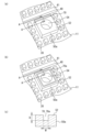
- FIG. 1A is a perspective view of a waveguide device according to a first embodiment
- FIG. 1B is a cross-sectional view taken along line AA of FIG.
- FIG. 2 is a perspective view of the waveguide device according to the first embodiment, seen through a second member.
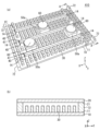
- FIG. 3A is a cross-sectional view of a waveguide device according to a comparative example
- FIG. 3B is a perspective view seen through a second member in the waveguide device according to the comparative example.
- 4A shows the results of simulation 1 of the comparative example
- FIG. 4B shows the results of simulation 1 of the first embodiment.
- FIG. 5A is a cross-sectional view of a waveguide device used in Simulation 2, and FIG. FIG.
- FIG. 6A is a cross-sectional view of a waveguide device used in Simulation 3
- FIG. 7A and 7B are cross-sectional views of waveguide devices according to first and second modifications of the first embodiment
- FIG. 7C is a perspective view showing a rod in a third modification of the first embodiment
- 8A to 8D are cross-sectional views of waveguide devices according to Modifications 4 to 7 of the first embodiment.
- FIG. 9A is a cross-sectional view of a waveguide device according to a second embodiment
- FIG. 9B is a perspective view of the waveguide device according to the second embodiment, in which a second member and a fixing member are seen through.
- FIG. 10 is a cross-sectional view showing a case where a recess is provided in a wall portion.
- FIG. 11(a) and 11(b) are cross-sectional views of the second embodiment in which a gap or a dielectric film is provided between the wall and the second member
- FIG. 11(c) and 11(d) are cross-sectional views of the second embodiment in which a gap or a dielectric film is provided between the wall and the first member
- 12(a) and 12(b) are perspective views showing the vicinity of a wall portion in Modifications 1 and 2 of Example 2
- FIG. 12(c) is a cross-sectional view of the wall portion taken along line AA in FIG. 12(a) and FIG. 12(b).
- FIG. 13A is a cross-sectional view of a waveguide device according to a third embodiment
- FIG. 13B is a perspective view seen through a second member in the waveguide device according to the third embodiment.
- FIG. 14A is a cross-sectional view of a waveguide device according to a fourth embodiment
- FIG. 14B is a perspective view seen through a second member in the waveguide device according to the fourth embodiment.
- FIG. 15A is a perspective view of a waveguide device according to a first modified example of the fourth embodiment, seen through a second member
- FIG. 15B is a cross-sectional view of the waveguide device according to the first modified example of the fourth embodiment.
- FIG. 16A is a perspective view of a waveguide device according to a second modification of the fourth embodiment, seen through a second member, and FIG.
- FIG. 16B is a cross-sectional view of the waveguide device according to the second modification of the fourth embodiment.
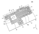
- FIG. 17 is a perspective view of a waveguide device according to a fifth embodiment, in which a second member and a fixing member are seen through.
- FIG. 18 is a perspective view of a waveguide device according to a sixth embodiment, in which a second member and a fixing member are seen through.
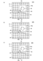
- 19A to 19C are plan views showing the second member and the fixing member in the waveguide devices according to the first to third modifications of the sixth embodiment.
- 20(a) and 20(b) are views of Example 6 and its modified example in which a gap is provided between the wall portion and the second member, and FIGS.
- FIG. 20(c) and 20(d) are views of the case in which a dielectric film is provided between the wall portion and the second member.
- FIG. 21 is a plan view showing a waveguide device according to a seventh embodiment, in which a second member and a fixing member are seen through the waveguide device.
- 22A and 22B are plan views showing a second member and a fixing member in a waveguide device according to an eighth embodiment and a modified example of the eighth embodiment.
- FIG. 23 is a cross-sectional view showing another example of the rod.
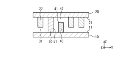
- FIG. 1(a) is a perspective view of a waveguide device 100 according to the first embodiment
- FIG. 1(b) is a cross-sectional view taken along the line A-A of FIG. 1(a).
- FIG. 2 is a perspective view of the waveguide device 100 according to the first embodiment, seen through the second member 20.
- FIG. 1(a), FIG. 1(b), and FIG. 2 show an XYZ coordinate system indicating mutually orthogonal X, Y, and Z directions.
- the Z direction is a direction perpendicular to the surface 11 of the first member 10 facing the second member 20.
- the X direction is a direction parallel to one direction in which the multiple rods 30 are arranged
- the Y direction is a direction parallel to the other direction.
- the waveguide device 100 includes a plate-like first member 10 and a plate-like second member 20 that extend along the XY plane, face each other in the Z direction, and are arranged substantially parallel to each other.
- the first member 10 has a conductive surface 11 (hereinafter referred to as the conductive surface 11) that faces the second member 20.
- the second member 20 has a conductive surface 21 (hereinafter referred to as the conductive surface 21) that faces the first member 10.
- the first member 10 and the second member 20 may be conductive members such as metal members, or a conductive film such as a metal film may be provided on the surface of an insulating member such as a resin.
- the waveguide device 100 further includes a waveguide member 40 having, for example, a ridge shape that is arranged on the conductive surface 11 of the first member 10, and a plurality of rods 30 arranged on both sides of the waveguide member 40.
- a waveguide member 40 having, for example, a ridge shape that is arranged on the conductive surface 11 of the first member 10, and a plurality of rods 30 arranged on both sides of the waveguide member 40.
- WRG Waffle iron Ridge Waveguide
- the waveguide member 40 is formed integrally with the first member 10 as a part of the first member 10, for example, and extends in the planar direction of the conductive surface 11 of the first member 10.
- integral includes the case where two members having conductive surfaces are continuously formed of the same material, for example, formed by integral molding of metal. Alternatively, it also includes the case where two members having conductive surfaces have a structure that maintains a contact state and are fixed with screws or the like.
- the waveguide member 40 may be a conductive member such as a metal member, like the first member 10, or a conductive film such as a metal film may be provided on the surface of an insulating member such as resin.
- the waveguide member 40 does not contact the second member 20, and is provided away from the conductive surface 21 of the second member 20.
- "contact" between two members having conductive surfaces refers to a state in which they are physically abutted and electrically conductive with each other.
- the surface of the waveguide member 40 facing the conductive surface 21 (the end face on the +Z direction side) is a conductive waveguide surface 41.
- the waveguide surface 41 extends in the direction in which the waveguide member 40 extends.
- a gap 42 is formed between the conductive surface 21 and the waveguide surface 41.
- a waveguide for the electromagnetic wave is formed in this gap 42. In other words, the electromagnetic wave propagates through the gap 42.
- the rods 30 are formed integrally with the first member 10 as a part of the first member 10, and extend from the conductive surface 11 toward the second member 20.
- the rods 30 have a conductive surface.
- the rods 30 may be a conductive member such as a metal member, as with the first member 10, or a conductive film such as a metal film may be provided on the surface of an insulating member such as a resin.
- a gap 31 is formed between the tip of the rod 30 and the conductive surface 21 of the second member 20, and the tip of the rod 30 does not contact the conductive surface 21.
- the tips of some of the rods 30 may be in contact with the conductive surface 21.
- the rods 30 are, for example, rectangular parallelepiped shaped.
- the arrangement periods T1 and T2 of the rods 30 are smaller than ⁇ 0 /2, for example , about ⁇ 0 /4, and for example, within the range of ⁇ 0 /4 ⁇ 0 /8, when the wavelength in free space of the electromagnetic wave propagating through the waveguide device 100 is ⁇ 0 .
- the arrangement periods T1 and T2 may be the same or different.
- the widths W1 and W2 of the rods 30 and the intervals D1 and D2 of the rods 30 are, for example, about ⁇ 0 /8, and for example, smaller than ⁇ 0 /4 and larger than ⁇ 0 /16.
- the widths W1 and W2 may be the same or different.
- the intervals D1 and D2 may also be the same or different.
- the rod 30 and the waveguide member 40 have substantially the same height H1, and the height H1 is, for example, larger than the widths W1 and W2 of the rod 30, and is, for example, about ⁇ 0 /4, and is, for example, within the range of ⁇ 0 /4 ⁇ 0 /8.
- the height of the gap 31 between the tip of the rod 30 and the conductive surface 21 and the height of the gap 42 between the waveguide surface 41 and the conductive surface 21 have substantially the same height H2, and the height H2 is, for example, about ⁇ 0 /8, and is, for example, smaller than ⁇ 0 /4.
- the reason for using the free space wavelength ⁇ 0 here is that the wavelength of the electromagnetic wave propagating within the waveguide device 100 is difficult to grasp because it can vary in various ways depending on the dimensions and shapes of each part of the device.
- the frequency band used in the waveguide device 100 is, for example, 30 GHz to 300 GHz.
- the waveguide device 100 also includes a wall portion 50 extending from the conductive surface 11 of the first member 10 toward the conductive surface 21 of the second member 20.
- the wall portion 50 is, for example, formed integrally with the first member 10 as a part of the first member 10, protrudes from the conductive surface 11, and contacts, for example, the conductive surface 21 of the second member 20 at its upper end (end in the +Z direction).
- the wall portion 50 may be a conductive member such as a metal member, as with the first member 10, or a conductive film such as a metal film may be provided on the surface of an insulating member such as a resin.
- the wall portion 50 is disposed adjacent to the waveguide member 40.
- the wall portion 50 faces the waveguide member 40 without any other member interposed therebetween.
- the wall portion 50 is disposed adjacent only to the straight portion of the waveguide member 40.
- adjacent refers to a state in which the wall portion 50 is disposed in close proximity to the waveguide member 40 through a space or a dielectric without sandwiching any other conductive object. In such a case, the distance between two adjacent members having conductive surfaces is, for example, about ⁇ 0 /4.
- the side surface 51 of the wall portion 50 facing the waveguide member 40 has an extension along the direction in which the waveguide member 40 extends.
- At least the side surface 51 of the wall portion 50 is conductive, and is electrically connected, for example, to the conductive surface 11 of the first member 10 and the conductive surface 21 of the second member 20.
- electrically connected includes not only the case where a part of the wall portion 50 is physically abutted against these conductive surfaces 11 and 21, but also the case where they are separated from each other with a non-conductive micro gap, are not conductive in terms of direct current, but are coupled in terms of high frequency in the frequency band used and are in a mutually conductive state. In this specification, this is referred to as a "high frequency coupled" state.
- This micro gap has a gap dimension of, for example, 100 ⁇ m or less (for example, ⁇ 0 /40 or less when the center frequency of the band used (operating frequency band) is 79 GHz), and this gap may be an air layer or a dielectric layer such as a non-conductive resin.
- the size of the minute gap where this high frequency coupling state occurs depends at least on the area of the two conductive surfaces that face each other across the minute gap. Therefore, even if two members with conductive surfaces are arranged with a minute gap of 100 ⁇ m or more, whether or not the state is high frequency coupled also depends on the structure at that time. This can be determined by the results of electromagnetic simulations at the design stage.
- the side surface 51 of the wall portion 50 extends along the waveguide member 40.
- the side surface 51 of the wall portion 50 extends along the waveguide member 40.
- the length L of the side surface 51 of the wall portion 50 in the direction along the waveguide member 40 (X direction) can be selected from various sizes, but is, for example, larger than the distance between the conductive surface 11 and the conductive surface 21 at the position of the wall portion 50.
- the length L of the side surface 51 of the wall portion 50 is preferably ⁇ 0 /2 or more, more preferably 3 ⁇ 0 /4 or more, and even more preferably ⁇ 0 or more.
- the width of the wall portion 50 in the Y direction is, for example, ⁇ 0 /8, but may be ⁇ 0 /4 or more.
- the length L is preferably at least twice the arrangement period T, more preferably at least three times, and even more preferably at least four times. In the example of Fig. 2, the length L is 4.5 times the arrangement period T of the multiple rods 30. It is also possible to use the length L at ⁇ 0 /2 or less.
- the upper edge of the side surface 51 of the wall 50 is preferably in contact with or high-frequency coupled to the conductive surface 21 of the second member 20, and is electrically conductive to the conductive surface 21. At least a part of the upper end (or upper surface, the same applies below) of the wall 50 is preferably in contact with or high-frequency coupled to the conductive surface 21 of the second member 20, and is electrically conductive to the conductive surface 21.
- the upper end of the wall 50 and the conductive surface 21 may not only be in contact with or in close contact with each other, but may also be part of the second member 20, or may be fixed together by diffusion bonding, caulking, screwing, or the like.
- a structure in which a conductive member, such as a conductive adhesive, conductive oil, conductive rubber, or elastic conductive resin, is interposed between the upper end of the wall 50 and the conductive surface 21 may be used.
- the upper end of the wall 50 and the conductive surface 21 may have a minute space or be electrically separated by a thin non-conductive film. Even in this case, if there is a high-frequency coupling state in the frequency band of the electromagnetic waves being used, the wall 50 can still suppress the leakage of electromagnetic waves. In other words, as long as the wall portion 50 has the effect of suppressing the leakage of electromagnetic waves, it is considered that the wall portion 50 and the second member 20 are in a high-frequency coupled state.
- FIG. 3(a) is a cross-sectional view of a waveguide device 1000 according to a comparative example
- Fig. 3(b) is a perspective view of the waveguide device 1000 according to the comparative example, seen through the second member 20.
- no wall portion is provided adjacent to the waveguide member 40.
- Rods 30 are also provided in the locations where the walls 50 were provided in Example 1.
- a plurality of rods 30 are provided adjacent to the waveguide member 40 on both sides of the waveguide member 40, and no wall portion is provided.
- the rods 30 are provided away from the second member 20 in order to suppress leakage of electromagnetic waves propagating through the gaps 42 on the waveguide member 40.
- the distance between the waveguide surface 41 and the conductive surface 21 it is necessary to set the distance between the waveguide surface 41 and the conductive surface 21 to the exact desired size. If the distance between the waveguide surface 41 and the conductive surface 21 changes and the height of the gap 42 on the waveguide member 40 differs from the desired size, the propagation characteristics of the electromagnetic waves may deteriorate.
- Example 1 as shown in Figures 1(b) and 2, the wall portion 50 is provided adjacent to the waveguide member 40 without the rod 30 in between.
- the distance between the first member 10 and the second member 20 near the waveguide member 40 is determined by the wall portion 50, so that the height of the gap 42 above the waveguide member 40 can be set to the desired size even if the first member 10 and/or the second member 20 is warped.
- Example 1 An electromagnetic simulation was performed to obtain S parameters for the waveguide devices according to Example 1 and the comparative example.
- the simulation conditions were as follows. Common conditions for Example 1 and Comparative Example Center frequency of the band used (operating frequency band): 79 GHz Width of the rod 30 in the X and Y directions: ⁇ 0 /8 Spacing between rods 30: ⁇ 0 /8 Height ⁇ 0 /4 of the rod 30 and the waveguide member 40 in the Z direction Distance between the rod 30 and the waveguide member 40: ⁇ 0 /8 Distance between the tips of the rod 30 and the waveguide member 40 and the conductive surface 21: ⁇ 0 /8
- Figure 4(a) shows the results of simulation 1 of the comparative example
- Figure 4(b) shows the results of simulation 1 of Example 1.
- the frequency characteristics of S11 are shown by solid lines
- the frequency characteristics of S21 are shown by dashed lines.
- S11 indicates the return loss, and indicates the degree of leakage of electromagnetic waves propagating through the gap 42 on the wave-guiding member 40.
- S11 indicating the return loss is slightly greater than -30 dB near 75 GHz, but is approximately -30 dB or less in the range from 75 GHz to 82 GHz. This shows the electromagnetic wave propagation blocking effect of the multiple rods 34.
- S11 indicating the return loss is -30 dB or less in the entire range from 75 GHz to 82 GHz. This is superior to the characteristics of the comparative example in Figure 4(a). In other words, when a wall portion 50 is provided adjacent to the wave guide member 40, it is found that the same or better electromagnetic wave propagation blocking effect can be obtained compared to when only the rod 30 is provided without the wall portion 50.
- Example 1 in addition to the waveguide on the waveguide member 40 formed by arranging a plurality of rods 30 on both sides of the waveguide member 40, a waveguide is also formed on the waveguide member 40 in the portion adjacent to the wall portion 50.
- the waveguide formed in the portion adjacent to the wall portion 50 is referred to as waveguide A.
- the waveguide A is formed by having one side adjacent to the wall portion 50 and the other side adjacent to the rod 30. Such a waveguide A has never been disclosed before and is a new waveguide. From the simulation results of Figures 4(a) and 4(b), it can be seen that the impedance of the waveguide A adjacent to the wall portion 50 is different from the impedance of the other waveguides sandwiched between the rods 30.
- the wall portion 50 by arranging the wall portion 50 and adjusting its length L, it is possible to adjust the phase of the signal wave propagating through the waveguide. It has also been found that in the portion where the side surface 51 of the wall portion 50 is adjacent to the waveguide member 40, the wavelength of the propagating electromagnetic wave is extended by about 3%. From this, it can be seen that the waveguide A is a novel waveguide that has never been seen before.
- the configuration in which the walls 50 are arranged at adjacent positions on both sides of the waveguide member 40 is the same as, for example, a waveguide having a ridge structure with an H-shaped cross section, and therefore can be understood to be within the scope of publicly known technology.
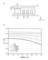
- FIG. 5(a) is a cross-sectional view of the waveguide device used in Simulation 2.
- the waveguide device used in Simulation 2 has a gap 80 formed between the wall portion 50 and the second member 20.
- the width of the wall portion 50 is different from that in Example 1.
- the other configurations are the same as those in Example 1.
- S parameters were obtained when the distance h between the wall portion 50 and the second member 20 was changed depending on the height of the gap 80.
- the simulation conditions are as follows.
- Figure 5(b) shows the results of simulation 2.
- Figure 5(b) shows the frequency characteristics of S21.
- the larger the interval h the more S21 deteriorates.
- the deterioration of S21 is suppressed to a level that does not impair the electromagnetic wave propagation blocking performance of the wall 50.
- the gap 80 is formed, if the decrease in S21 due to the gap 80 is within the range allowable for the intended use, it can be said that the wall 50 and the second member 20 are in a high-frequency coupled state.
- the decrease in S21 varies depending on the opposing area and interval between the wall 50 and the second member 20, and whether the decrease in S21 is within the allowable range varies depending on the characteristics expected of the waveguide depending on the intended use and required performance.
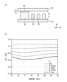
- FIG. 6(a) is a cross-sectional view of the waveguide device used in Simulation 3.
- the waveguide device used in Simulation 3 has a dielectric film 82 provided between the wall portion 50 and the second member 20.
- the width of the wall portion 50 is different from that in Example 1.
- the other configurations are the same as those in Example 1.
- S parameters were obtained when the distance h between the wall portion 50 and the second member 20 was changed depending on the thickness of the dielectric film 82.
- the simulation conditions are as follows.
- Figure 6(b) shows the results of Simulation 3.
- Figure 6(b) shows the frequency characteristics of S21.
- the dielectric film 82 is provided between the wall 50 and the second member 20
- the larger the distance h the more S21 deteriorates.
- the distance h is sufficiently small compared to the wavelength, it can be seen that the deterioration of S21 is suppressed to a level that does not impair the electromagnetic wave propagation blocking performance of the wall 50.
- the dielectric film 82 is provided, if the decrease in S21 due to the dielectric film 82 is within the range acceptable for the intended use, it can be said that the wall 50 and the second member 20 are in a high-frequency coupled state.
- the decrease in S21 varies depending on the opposing area and distance between the wall 50 and the second member 20, and whether the decrease in S21 is within the acceptable range varies depending on the characteristics expected of the waveguide depending on the intended use and the required performance.
- the wall portion 50 is provided adjacent to the waveguide member 40 without the rod 30 therebetween.
- the wall portion 50 is provided between the conductive surface 11 of the first member 10 and the conductive surface 21 of the second member 20 by contacting or high-frequency coupling with the conductive surface 11 and the conductive surface 21.
- the distance between the first member 10 and the second member 20 in the vicinity of the waveguide member 40 is determined by the wall portion 50, so that even if the first member 10 and/or the second member 20 are warped, the height of the gap 42 on the waveguide member 40 can be set to a desired size.
- the side surface 51 of the wall portion 50 facing the waveguide member 40 is conductive. Therefore, the wall portion 50 can function as an electric wall, and a good electromagnetic wave propagation blocking effect can be obtained as shown in FIG. 4(b).
- the length L of the wall 50 along the waveguide 40 in the surface direction of the conductive surface 11 is greater than the distance between the conductive surface 11 and the conductive surface 21 at the position of the wall 50. This prevents the difference between the length L of the wall 50 and the width W1 of the rod 30 in the direction along the waveguide 40 from becoming small, and prevents the effect of suppressing the lateral leakage of electromagnetic waves propagating through the gap 42 on the waveguide 40 from being disturbed, so that a good electromagnetic wave propagation blocking effect can be obtained for the electromagnetic waves propagating through the gap 42.
- the length L is preferably 1.5 times or more, more preferably 2.0 times or more, and even more preferably 2.5 times or more, of the distance between the conductive surface 11 and the conductive surface 21.
- the length L is preferably 5 times or less, more preferably 4 times or less, and even more preferably 3 times or less, the distance between the conductive surface 11 and the conductive surface 21.
- the length L of the wall 50 along the waveguide 40 in the surface direction of the conductive surface 11 is greater than ⁇ 0 /2, where ⁇ 0 is the free space wavelength at the center frequency of the band used by the waveguide device 100. This prevents the difference between the length L of the wall 50 and the width W1 of the rod 30 in the direction along the waveguide 40 from becoming small, and prevents the effect of suppressing lateral leakage of electromagnetic waves propagating through the gap 42 on the waveguide 40 from being disturbed, thereby providing a good electromagnetic wave propagation blocking effect for electromagnetic waves propagating through the gap 42.
- the length L is preferably 3 ⁇ 0 /4 or more, more preferably ⁇ 0 or more, and even more preferably 5 ⁇ 0 /4 or more.
- the length L is preferably 3 ⁇ 0 or less, more preferably 2.5 ⁇ 0 or less, and even more preferably 2.0 ⁇ 0 or less.
- Example 1 as shown in FIG. 2, the side surface 51 of the wall portion 50 extends along the wave guide member 40. This enhances the function of the wall portion 50 as an electric wall, and provides a good electromagnetic wave propagation blocking effect.
- Example 1 as shown in FIG. 2, the side surface 51 of the wall portion 50 is adjacent to the straight portion of the wave guide member 40. This makes it easier for the wall portion 50 to function as an electric wall, and makes it easier to obtain a good electromagnetic wave propagation blocking effect.
- some of the rods 30 are provided adjacent to the waveguide 40 on the opposite side of the waveguide 40 from the wall 50. This makes it possible to suppress lateral leakage of electromagnetic waves propagating through the gap 42 above the waveguide 40, and to obtain a good electromagnetic wave propagation blocking effect against electromagnetic waves propagating through the gap 42.
- Example 1 some of the rods 30 are provided on both sides of the wall portion 50 in the direction in which the waveguide member 40 extends. This makes it possible to suppress lateral leakage of electromagnetic waves propagating through the gap 42 above the waveguide member 40, and to obtain a good electromagnetic wave propagation blocking effect against electromagnetic waves propagating through the gap 42.
- FIG. 7(a) and 7(b) are cross-sectional views of the waveguide devices 110 and 120 according to the first and second modifications of the first embodiment
- FIG. 7(c) is a perspective view showing the rod 30 according to the third modification of the first embodiment.
- the edge portions of the rod 30, the waveguide member 40, and the wall portion 50 are R-shaped (corner round).
- the R-shape may be chamfered.
- the rod 30, the waveguide member 40, and the wall 50 have a shape that gradually tapers from the conductive surface 11 toward the conductive surface 21.
- the side surfaces of these members are tapered.
- the gradually tapering shape of the rod 30, the waveguide member 40, and the wall 50 increases the ease of molding when the rod 30, the waveguide member 40, and the wall 50 are molded together with the first member 10 using resin or metal.
- this tapering shape is not limited to the case where it becomes continuously tapered, but may be a shape that becomes tapered once and then maintains the same thickness, or may be a shape that becomes tapered again. It is sufficient that the shape does not have at least a gradually thickening portion.
- the rod 30 in the third modified example of the first embodiment has a cylindrical shape. That is, the rod 30 has a circular shape in a plan view. Electromagnetic simulations have confirmed that making the rod 30 cylindrical has the effect of improving the frequency characteristics in electromagnetic wave propagation, particularly the operating band. Note that the rod 30 may have an elliptical cylindrical shape, that is, an elliptical shape in a plan view, or may have an oval shape in a plan view.
- the rounded structures such as the R-shape (corner radius) of the edge portion and the chamfered structure described in Variation 1 of Example 1, the tapered structure described in Variation 2 of Example 1, and the cylindrical structure described in Variation 3 of Example 1 can also be applied to Examples 2 and onward.
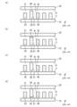
- FIG. 8(a) to 8(d) are cross-sectional views of modified examples 4 to 7 of the first embodiment.
- a gap 80 may be formed between the wall 50 and the second member 20.
- a dielectric film 82 may be provided between the wall 50 and the second member 20.
- a gap 80 may be formed between the wall 50 and the first member 10.
- a dielectric film 82 may be provided between the wall 50 and the first member 10.
- the wall 50 and the first member 10 or the second member 20 are in a high-frequency coupled state.
- the gap 80 or the dielectric film 82 may be provided between the wall 50 and both the first member 10 and the second member 20.
- the height of the gap 80 and the thickness of the dielectric film 82 are dimensions that realize high frequency coupling, for example, ⁇ 0 /40 or less.
- FIG. 9(a) is a cross-sectional view of the waveguide device 200 according to the second embodiment
- FIG. 9(b) is a perspective view of the waveguide device 200 according to the second embodiment, seen through the second member 20 and the fixing member 60.
- FIG. 9(a) shows a cross-section of a portion corresponding to A-A in FIG. 9(b).
- the waveguide device 200 according to the second embodiment has two waveguide members 40.
- the two waveguide members 40 both extend in the X direction and are aligned with each other in the Y direction.
- Two wall portions 50a are provided adjacent to each of the two waveguide members 40.
- the two wall portions 50a adjacent to one of the two waveguide members 40 are located on the opposite side of the other waveguide member 40 across the other waveguide member 40.
- the two wall portions 50a adjacent to the other waveguide member 40 are located on the opposite side of the other waveguide member 40 across the other waveguide member 40.
- the wall portions 50a are provided with a through hole 54 penetrating between an upper end 52 that contacts or is high-frequency coupled with the conductive surface 21 of the second member 20 and a lower end 53 opposite the upper end 52.
- the first member 10 is provided with a through hole 13 penetrating the first member 10
- the second member 20 is provided with a through hole 23 penetrating the second member 20.
- the waveguide device 200 has a fixing member 60.
- the fixing member 60 is, for example, a screw such as a bolt.
- the fixing member 60 is integrally formed of a shaft portion 61 and a umbrella portion 62.
- the shaft portion 61 passes through the through hole 23 of the second member 20, the through hole 54 of the wall portion 50a, and the through hole 13 of the first member 10, and exits in the -Z direction of the first member 10, where a fixing member 63 such as a nut is tightened and fixed.
- the umbrella portion 62 is disposed on the +Z direction side of the second member 20, and receives the tightening pressure transmitted to the shaft portion 61 and transmits it to the second member 20, thereby fixing the second member 20 to the wall portion 50a.
- the shaft portion 61 may be fixed by fitting a male thread provided on the shaft portion 61 into a female thread provided on the inner surface of the through hole 54 of the wall portion 50, or may be fixed by other fixing methods.
- the rest of the configuration is the same as in Example 1, so the explanation will be omitted.
- a typical WRG waveguide device is composed of multiple layers. These layers are assembled with a fixed distance between them using fixing means such as bolts. In conventional WRG waveguide devices, this distance in the Z direction is ensured by using members such as spacers placed between each layer, or by integrating spacers into each layer. Such spacers are provided outside the waveguiding region, as in Patent Document 1.
- the second member 20 is fixed to the wall 50a provided adjacent to the waveguide member 40 by the fixing member 60. That is, the second member 20 is pressed against the wall 50a by the fixing member 60, and the upper end 52 of the wall 50a and the conductive surface 21 of the second member 20 are in close contact with each other.
- the wall 50a serves as a spacer.
- the spacer is disposed outside the waveguide region, so that it is necessary to secure a region for providing the spacer on the outer periphery of the waveguide device. This results in an increase in the size of the waveguide device.
- the wall 50a provided in the waveguide region adjacent to the waveguide member 40a functions as a spacer, so that the waveguide device 200 can be made smaller.
- the conductive surface 11 of the first member 10 and the conductive surface 21 of the second member 20 are electrically connected via the wall portion 50a, which improves the effect of suppressing leakage of electromagnetic waves.
- the wall 50a has a through hole 54 at the upper end 52 that contacts the conductive surface 21 of the second member 20.
- the second member 20 is fixed to the wall 50a by inserting a fixing member 60 into the through hole 54.
- a recess 59 having a bottom surface may be provided at the upper end 52 of the wall 50a as shown in FIG. 10, and the fixing member 60 may be inserted into this recess 59.
- the through hole 54 and the recess 59 are not limited to being provided at the upper end 52 that contacts the conductive surface 21, and may be provided on the upper surface that does not contact the conductive surface 21.
- a gap 80 or a dielectric film 82 may be provided between the wall 50a and the second member 20.
- a gap 80 or a dielectric film 82 may be provided between the wall 50a and the first member 10 or the second member 20. Even if a gap 80 or a dielectric film 82 is provided between the wall 50a and the first member 10 or the second member 20 as described above, if the decrease in S21 due to the gap 80 or the dielectric film 82 is within an allowable range for the intended use, it can be said that the wall 50a and the first member 10 or the second member 20 are in a high-frequency coupling state.
- the gap 80 or the dielectric film 82 may be provided between the wall 50a and both the first member 10 and the second member 20. In Figs. 11(a) to 11(d), the fixing member 60 and the like are omitted for clarity.
- the conductive surface 21 of the second member 20 is in contact only with the upper ends 52 of the four wall portions 50a.
- the portion corresponding to the spacer is realized by a peripheral wall that is the outer shell of the member corresponding to the first member 10 and is provided outside the waveguiding region on the outside of the rod. That is, the upper end of this peripheral wall abuts against the lower surface of the member corresponding to the second member 20, thereby securing a gap of the height of this peripheral wall. Comparing the structure of Patent Document 1 with the structure of Example 2, the size of the waveguide device in Patent Document 1 is larger by the area of the peripheral wall.
- the member corresponding to the first member 10 and the member corresponding to the second member 20 are fixed only at the peripheral wall portion on the outer periphery, so that if there is warping in the central portion of these members, the gap between the two members in the central portion changes.
- the wall portion 50a is provided within the waveguiding region, that is, inside the rod 30.
- the wall portion 50a can be provided within any waveguiding region. This allows the height of the gap 42 between the waveguide surface 41 of the waveguide member 40 and the conductive surface 21 of the second member 20 to be a more uniform and accurate dimension, even if there is warping in the center, for example.
- the return loss of the waveguide device 200 according to the second embodiment was determined by electromagnetic simulation. As a result, S11, which indicates the return loss, was -28 dB or less over the entire range from 75 GHz to 82 GHz. In other words, even when a wall portion 50a large enough to allow the fixing member 60 to be inserted is used, the wall portion 50a has a sufficient effect of suppressing electromagnetic wave leakage, and the waveguide device 200 has excellent transmission characteristics.
- FIG. 12(a) and 12(b) are perspective views showing the vicinity of the wall portion 50a in the first and second modified examples of the second embodiment
- FIG. 12(c) is a cross-sectional view of the wall portion taken along line A-A in FIG. 12(a) and FIG. 12(b).
- a groove 70 is provided at the upper end 52 of the wall portion 50a, located between the through hole 54 and the waveguide member 40. The groove 70 extends along the direction in which the waveguide member 40 extends.
- the waveguide member 40 extends includes a case in which the groove 70 and the waveguide member 40 are completely parallel to each other, and also a case in which the groove 70 is inclined within a range of 30° or less with respect to the waveguide member 40.
- the groove 70 opens, for example, on both opposing side walls of the wall portion 50a, but may not reach both side walls.
- the depth D of the groove 70 is, for example, ⁇ 0 /4.
- the other configurations are the same as those of the second embodiment, and therefore will not be described.
- the groove 70 forms a waveguide in the depth direction. Electromagnetic waves that enter the groove 70 propagate in the depth direction of the groove 70 and are reflected at the bottom. When the reflected electromagnetic waves return to the entrance of the groove 70, their phase changes by 180° from when they entered. As a result, the reflected electromagnetic waves reflected at the bottom of the groove 70 and the invading electromagnetic waves that enter the groove 70 cancel each other out, and the electromagnetic waves are attenuated. This is the effect of the groove 70's electromagnetic wave propagation blocking action.
- the width W of the groove 70 is not particularly limited, but may be, for example, ⁇ 0 /4 or less, for example, about ⁇ 0 /8.
- the groove 70 may be formed at the upper end 52 of the wall portion 50a, located outside the through hole 54 and inside the side wall on the waveguide member 40 side.
- the side surface of the groove 70 may have a tapered shape that gradually widens from the bottom. This tapered shape may not only have a width that continuously widens as the height from the bottom increases, but may also have a constant width in some parts without widening. In other words, the tapered shape may have a shape in which the width at least does not narrow as the height from the bottom increases.
- the groove 70a is provided surrounding the through hole 54. That is, the groove 70a is located outside the through hole 54 and inside the side wall of the wall 50a, and is provided on the upper end 52 of the wall 50a so as to surround the through hole 54.
- the shape of the groove 70a may be a rectangle with rounded corners or a circle.
- the groove 70a may also have a tapered shape like the groove 70.
- the other configurations are the same as those of the second embodiment, and therefore a description thereof will be omitted.
- the return loss of the waveguide devices according to the first and second variations of the second embodiment was determined by electromagnetic simulation. As a result, S11, which indicates the return loss, was -30 dB or less over the entire range from 75 GHz to 82 GHz. This confirmed the electromagnetic wave leakage blocking effect of the grooves 70 and 70a.
- the depth D of the grooves 70, 70a is preferably ⁇ 0 /4, but may be within the range of ⁇ 0 /4 ⁇ ⁇ 0 /8. Simulation results and actual measurement results have shown that the depth D of the grooves 70, 70a is effective in blocking electromagnetic wave propagation when it is within the range of ⁇ 0 /4 ⁇ ⁇ 0 /8. Specifically, the depth D that realizes the optimal blocking effect in relation to the surrounding parts can be selected at the design stage.
- the wall portion 50a has grooves 70, 70a at the upper end 52, which are located between the through hole 54 and the waveguide member 40 and extend in the direction in which the waveguide member 40 extends.
- the depth D of the grooves 70, 70a is within the range of ⁇ 0 /4 ⁇ ⁇ 0 /8. This allows electromagnetic waves penetrating the grooves 70, 70a to be attenuated by canceling out electromagnetic waves that have entered the grooves 70, 70a and been reflected at the bottom. This makes it possible to prevent electromagnetic waves propagating through the gap 42 above the waveguide member 40 from leaking out of the through hole 54.
- a groove 70a is provided surrounding the through hole 54. This makes it possible to further suppress the leakage of electromagnetic waves.
- the grooves 70 and 70a shown in the first and second variations of the second embodiment can also be applied to the other embodiments. By applying the grooves 70 and 70a, it is possible to further reduce electromagnetic wave leakage, and to realize a high-performance waveguide device.
- the waveguide device 300 according to the third embodiment includes two waveguide members 40 each extending in the X direction and arranged in the Y direction, as in the second embodiment.
- Two walls 50a are provided between the two waveguide members 40.
- Each of the two walls 50a is adjacent to both of the two waveguide members 40, and has a side 51a that extends in the direction in which one waveguide member 40 extends, and a side 51b that extends in the direction in which the other waveguide member 40 extends.
- the side surfaces 51a and 51b face the waveguide members 40, and no other members such as a rod 30 are provided between the waveguide members 40. Electromagnetic waves propagating through the gap 42 above the waveguide 40 are less likely to leak to the side due to the electromagnetic wave propagation blocking function provided by the wall 50a and rod 30 arranged on the side of the waveguide 40.
- the rest of the configuration is the same as in Example 2, so a description will be omitted.
- the return loss of the waveguide device 300 according to Example 3 was determined by electromagnetic simulation. As a result, S11, which indicates the return loss, was -30 dB or less over the entire range from 75 GHz to 82 GHz. In other words, it was confirmed that the wall portion 50a has a sufficient effect of blocking electromagnetic wave leakage, and the waveguide device 300 has excellent transmission characteristics.
- the wall portion 50a is provided adjacent to both of the two waveguide members 40. This allows the number of wall portions 50a to be reduced, and the waveguide device 300 can be further miniaturized.
- the waveguide device 400 according to the fourth embodiment includes three waveguide members 40 each extending in the X direction and arranged in the Y direction, and three walls 50a provided between the waveguide members 40.
- the three walls 50a are arranged in a zigzag pattern.
- Each of the three walls 50a is adjacent to the waveguide member 40 and has a side surface 51 that extends in the direction in which the waveguide member 40 extends.
- the side surface 51 faces the waveguide member 40, and no other members such as the rod 30 are interposed between them.
- the first member 10 is provided with a through hole 14 that is adjacent to the tip of the waveguide member 40 and penetrates the first member 10.
- the through hole 14 has a conductive inner surface.
- the through hole 14 serves to connect the waveguide provided in the layer below the first member 10 to the waveguide formed in the gap 42 above the waveguide member 40.
- the rest of the configuration is the same as in Example 2, so a description thereof will be omitted.
- Example 4 the end of the waveguide member 40 is cut off for convenience of explanation, and the outside is excluded from the explanation.
- a through hole 14 is provided in the first member 10 adjacent to the tip of the waveguide member 40.
- electromagnetic waves propagating through the gap 42 on the waveguide member 40 are input from the through hole 14 adjacent to one tip of the waveguide member 40 and output from the through hole 14 adjacent to the other tip.
- Two rows of rods 30 are provided on the outer lateral sides of the through hole 14, resulting in a structure that has the effect of blocking electromagnetic wave propagation.
- the return loss of the waveguide device 400 according to Example 4 was determined by electromagnetic simulation. As a result, S11, which indicates the return loss, was -30 dB or less over the entire range from 75 GHz to 82 GHz. In other words, it was confirmed that the wall portion 50a has a sufficient electromagnetic wave leakage blocking effect, and the waveguide device 400 has excellent transmission characteristics.
- Example 4 the first member 10 and the second member 20 are fixed to each other while maintaining a distance therebetween only by three walls 50a and three fixing members 60.
- Example 2 A similar configuration was described in FIG. 9(a) and FIG. 9(b) of Example 2, but in Example 2, for example, a member not shown may be present outside the end of the waveguide member 40.
- the waveguide device 400 of Example 4 is a waveguide device closed within a pair of layers formed by the first member 10 and the second member 20. No other members are present in the outer shell of the first member 10 and the second member 20. In such a waveguide device 400, only three walls 50a and three fixing members 60 are used as a means for fixing the first member 10 and the second member 20. This is different from the conventional WRG waveguide device described in the above-mentioned Patent Document 1 and the like. As a result, the effect of miniaturizing the waveguide device 400 can be obtained, as in Example 2.
- FIG. 15(a) is a perspective view of the second member 20 in the waveguide device 410 according to the first modification of the fourth embodiment
- FIG. 15(b) is a cross-sectional view of the waveguide device 410 according to the first modification of the fourth embodiment
- FIG. 15(b) is a cross-sectional view of a portion corresponding to the A-A section in FIG. 15(a).
- pillars 72 having a width wider than the rods 30 provided around the waveguide member 40 are provided at the four corners of the first member 10.
- the pillars 72 have the same height as the wall 50a. Therefore, the pillars 72 are in contact with the conductive surface 11 of the first member 10 and are in contact with the conductive surface 21 of the second member 20.
- the other configurations are the same as those in the fourth embodiment, and therefore will not be described.
- FIG. 16(a) is a perspective view of the second member 20 in a waveguide device 420 according to the second modification of the fourth embodiment
- FIG. 16(b) is a cross-sectional view of the waveguide device 420 according to the second modification of the fourth embodiment
- FIG. 16(b) is a cross-sectional view of a portion corresponding to A-A in FIG. 16(a).
- pillars 72a instead of the pillars 72, pillars 72a having a width similar to that of the rod 30 are provided at the four corners of the first member 10.
- the pillars 72a have the same height as the wall 50a, similar to the pillars 72, and are in contact with the conductive surface 11 of the first member 10 and the conductive surface 21 of the second member 20.
- the other configurations are the same as those in the fourth embodiment, and therefore will not be described.
- the gap between the first member 10 and the second member 20 is adjusted by the three wall portions 50a and the four pillar portions 72 or 72a.
- the pillar portions 72 and 72a are effective when the outer shell of the first member 10 is warped in a direction that narrows the gap relative to the second member 20.
- the pillar portions 72 and 72a like the rod 30, also have the function of suppressing leakage of electromagnetic waves propagated inside the waveguide device.
- the pillar portions 72 and 72a are installed within the waveguiding region.
- the pillar portions 72 and 72a are not limited to being installed at the four corners, and may be installed at any two corners, for example, two corners located diagonally. They may also be installed at one location where warping is particularly a concern.
- the column portion 72 is wider than the rod 30, it can withstand strong stress when the second member 20 abuts against it.
- the waveguide device 500 according to the fifth embodiment includes a waveguide member 40a bent in an L-shape in addition to the straight waveguide member 40. Adjacent to the straight waveguide member 40 are a wall portion 50 without a through hole and a wall portion 50a with a through hole 54. Furthermore, adjacent to the tip of the waveguide members 40, 40a, a through hole 14 is provided that penetrates the first member 10 and has the function of connecting the waveguide formed on the waveguide members 40, 40a to the waveguide in the layer below the first member 10.
- the other configurations are the same as those of the second embodiment, so a description thereof will be omitted.
- the fixing member 60 is inserted into the through hole 54 in the wall 50a, so that the upper end of the wall 50a abuts against the conductive surface 21 of the second member 20, and the size of the gap between the first member 10 and the second member 20 is determined. Since the wall 50a is adjacent to the waveguide member 40, the wall 50a determines the gap between the first member 10 and the second member 20, and the height of the gap 42 between the waveguide surface 41 of the waveguide member 40, 40a and the conductive surface 21 of the second member 20 can be set to a desired size. In addition, the wall 50, which has a width approximately equal to that of the rod 30, is provided adjacent to the waveguide member 40 at a position away from the wall 50a.
- the conductive surface 21 of the second member 20 also abuts against the upper end of the wall 50. As a result, the size of the gap between the first member 10 and the second member 20 in the range where the first member 10 and the second member 20 face each other can be made uniform.
- a wide wall portion 50a having a through hole 54 into which the fixing member 60 is inserted and a thin wall portion 50 having no through hole.
- the wall portion 50a plays two roles: determining the distance between the first member 10 and the second member 20, and fixing the second member 20 to the wall portion 50a.
- the wall portion 50a may be provided adjacent to the waveguide member 40 or the waveguide member 40a, and may have a sufficient space for disposing the wide wall portion 50a. For example, if the frequency of the electromagnetic wave used is in the band of 76 GHz to 81 GHz, the free space wavelength ⁇ 0 is approximately 4 mm.
- the arrangement period T of the rods 30 is generally selected to be a value of about ⁇ 0 /4.
- the upper end of the wall portion 50a having the through hole 54 may be a square having a size of, for example, 4 mm or more.
- the length of the side surface 51 of the wall portion 50a facing the waveguide member 40 is 4 mm or more, which is a dimension that is approximately equal to or greater than the free space wavelength ⁇ 0. This determines the length of the wall portion 50a having the through hole 54 into which the fixing member 60 is inserted, in the direction along the waveguide member 40.
- the length of the side surface 51 of the wall portion 50 having no through holes, facing the wave-guiding member 40 is preferably at least twice the arrangement period T of the rods 30, as described in the first embodiment.
- the side surface 51 is ⁇ 0 /2 or less, there is an effect of blocking electromagnetic wave propagation. Therefore, it is also possible to use the side surface 51 with a length of ⁇ 0 /2 or less.
- the length and thickness of the wall portion 50 having no through holes can be freely selected. It can be made thicker when a relatively large strength is required.
- the arrangement of the wall portion 50 can also be freely selected.
- the WRG allows for three-dimensional waveguide arrangements. Therefore, it is possible to freely design which positions of the multiple waveguide layers that make up the waveguide device are fixed at, and at which positions the walls determine the spacing between the first and second members. By taking advantage of this design freedom, it is possible to place the walls in the most effective positions. In this way, by taking advantage of the freedom of waveguide design in the WRG, it is possible to optimize the placement of the walls. This makes it possible to assemble a waveguide device as designed, resulting in a high-performance waveguide device.
- FIG. 18 is a perspective view of the second member 20 and the fixing member 60 in the waveguide device 600 of Example 6.
- FIG. 18 shows a part of the waveguide device 600 of Example 6.
- the L-shaped waveguide member 40a is bent into a quarter-circular arc.
- a wall portion 50a is provided adjacent to the outside of the bent portion 43 of the waveguide member 40a.
- the wall portion 50a has a recess 55 recessed toward the center of the wall portion 50a to correspond to the bent portion 43 of the waveguide member 40a.
- the side surface 56 of the recess 55 of the wall portion 50a faces the outer side surface of the bent portion 43 of the waveguide member 40a.
- no other members such as the rod 30 are arranged between the side surface 56 of the wall portion 50a and the waveguide member 40a.
- the side surface 56 of the wall portion 50a has a portion that is curved in a quarter-circular arc shape to fit along the quarter-circular arc-shaped bend portion 43 of the wave guide member 40a.
- the impedance of the waveguide formed on the waveguide surface 41 of the waveguide member 40a changes at the bent portion 43 that bends in a quarter-circular arc shape of the waveguide member 40a.
- a recess 44 is provided on the upper surface of the bent portion 43 to match the impedance at the straight portion.
- the rods 30 are provided in the regions on both sides of the waveguide member 40a, except for the region between the side surface 56 of the wall portion 50a and the waveguide member 40a. Of the rods 30, the rod 30a facing the inner side surface of the bent portion 43 of the waveguide member 40a has a different shape from the other rods 30.
- the side surface of the rod 30a facing the waveguide member 40a is curved in a quarter-circular arc shape so as to follow the bent portion 43 of the waveguide member 40a.
- the impedance at the quarter-circular arc-shaped bent portion 43 can be adjusted.
- the side surface 56 of the wall portion 50a curved so as to follow the bend 43, the impedance of the electromagnetic waves propagating on the waveguide surface 41 of the waveguide member 40a can be adjusted.
- the bent portion 43 of the waveguide member 40a is bent in a quarter-circular arc shape, but it may be bent in other curved shapes, such as an elliptical arc shape or a free-form curve.
- [Modification] 19(a) to 19(c) are plan views of the second member 20 and the fixing member 60 in the waveguide devices 610 to 630 according to the first to third modifications of the sixth embodiment.
- FIGS. 19(a) to 19(c) also show a part of the waveguide devices 610 to 630 according to the first to third modifications of the sixth embodiment.
- the bending portion 43 of the waveguide member 40a is bent at a right angle in a plan view, and the outer corners are chamfered, and the side surface 45 is formed by chamfering. That is, the bending portion 43 is bent linearly in a plan view.
- the side surface 56 of the recess 55 of the wall portion 50a is curved in a quarter semicircular arc shape in a plan view, similar to FIG. 17. That is, in the first modification of the sixth embodiment, the curved side surface 56 faces the outer side surface 45 of the bending portion 43 bent linearly.
- the impedance at the bent portion 43 of the waveguide 40a is matched to the impedance at the straight portion of the waveguide 40a by the recess 44 provided on the upper surface of the bent portion 43 and the side surface 45 formed by chamfering the bent portion 43.
- the rod 30 is provided in a region adjacent to the outer side wall of the wall portion 50a so as to surround the wall portion 50a.
- the bent portion 43 of the waveguide 40a may be bent in a straight line, and the side surface 56 of the recess 55 of the wall portion 50a may be curved.
- the bent portion 43 of the waveguide member 40a is bent at a right angle in a plan view, and the outer corners are chamfered to form side surfaces 45, as in the first modification of the sixth embodiment.
- the side surfaces 56 of the recess 55 of the wall portion 50a are formed in a straight line in a plan view so as to face along the bent portion 43.
- the rod 30 is provided in a region adjacent to the outer side wall of the wall portion 50a so as to surround the wall portion 50a.
- the bent portion 43 of the waveguide member 40a may be bent in a straight line, and the side surfaces 56 of the recess 55 of the wall portion 50a may be straight, with the straight portions facing each other.
- the bent portion 43 of the waveguide member 40a is bent in a curved shape in a planar view, as in the sixth embodiment.
- the side surface 56 of the recess 55 of the wall portion 50a is formed in a straight line in a planar view, as in the second modification of the sixth embodiment.
- a rod 30 is provided in an area adjacent to the outer side wall of the wall portion 50a so as to surround the wall portion 50a.
- the bent portion 43 of the waveguide member 40a may be bent in a curved shape, and the side surface 56 of the recess 55 of the wall portion 50a may be straight.
- the waveguide member 40a includes a bent portion 43 where the extension direction of the waveguide member 40a changes.
- the side surface 56 of the wall portion 50a includes a part of the bent portion 43 and is adjacent to the waveguide member 40a. Even in this case, the wall portion 50a functions as an electric wall, and an electromagnetic wave propagation blocking effect is obtained.
- the shape of the bent portion 43 of the waveguide member 40a and the shape of the side surface 56 of the wall portion 50a can be appropriately changed to adjust the impedance.
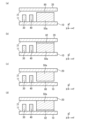
- a gap 80 may be formed between the wall 50a and the second member 20 as shown in Figs. 20(a) and 20(b), or a dielectric film 82 may be provided between the wall 50a and the second member 20 as shown in Figs. 20(c) and 20(d).
- a gap 80 or a dielectric film 82 may be provided between the wall 50a and the first member 10. Even in these cases, if the decrease in S21 due to the gap 80 or the dielectric film 82 is within an allowable range for the intended use, it can be said that the wall 50a and the first member 10 or the second member 20 are in a high-frequency coupled state.
- Figs. 20(a) and 20(c) are exploded perspective views, and in Figs. 20(b) and 20(d), the fixing member 60 and the like are omitted for clarity.
- FIG. 21 is a plan view of the second member 20 and the fixing member 60 in the waveguide device 700 of the seventh embodiment.
- the wall portion 50a is provided adjacent to the inside of the bent portion 43 of the waveguide member 40a. Since the through hole 14 adjacent to the tip of the waveguide member 40a is arranged near the wall portion 50a, a cutout portion 57 is provided in the wall portion 50a. As a result, two rows of rods 30 are arranged between the through hole 14 and the wall portion 50a, and an electromagnetic wave propagation blocking effect is obtained. In this way, the wall portion 50a does not need to be square in plan view. Any shape can be adopted as necessary while taking into account the simulation results at the time of design.
- the corner of the wall portion 50a facing the bent portion 43 of the waveguide member 40a is a corner radius 58.
- a corner radius 58 By forming a corner radius 58 at the corner of the wall 50a facing the bent portion 43 of the waveguide member 40a, it is possible to adjust the impedance of the electromagnetic waves propagating on the waveguide surface 41 of the waveguide member 40a.
- the wall portion 50a may be disposed adjacent to the outside of the bent portion 43 of the wave guide member 40a, as in Example 6 and its modified example, or may be disposed adjacent to the inside of the bent portion 43, as in Example 7. In either case, the wall portion 50a functions as an electric wall, and provides the effect of blocking electromagnetic wave propagation.
- FIG. 22(a) is a plan view of the second member 20 and the fixing member 60 in a waveguide device 800 according to Example 8
- FIG. 22(b) is a plan view of the second member 20 and the fixing member 60 in a waveguide device 810 according to a modified example of Example 8.
- the waveguide device 800 according to Example 8 and the waveguide device 810 according to a modified example of Example 8 include a waveguide member 40b having a T-shaped branching portion 46.
- the wall portion 50a may be disposed on the head side (outside) of the T-shaped branching portion 46, or may be disposed at one of the side corners of the T-shaped branching portion 46.
- the waveguide members 40 to 40b may be part of the second member 20 and may protrude from the conductive surface 21 toward the conductive surface 11. Even in this case, the tip surfaces of the waveguide members 40 to 40b become the waveguide surface 41, and electromagnetic waves propagate through the gap 42 between the waveguide surface 41 and the conductive surface 11.
- the multiple rods 30 may be part of the first member 10 and protrude from the conductive surface 11 toward the conductive surface 21 as shown in FIG. 1(b), with a gap 31 between them and the conductive surface 21, or may be part of the second member 20 and protrude from the conductive surface 21 toward the conductive surface 11 as shown in FIG. 23, with a gap 31 between them and the conductive surface 11.
- the waveguide members 40-40b are part of the first member 10 and protrude from the conductive surface 11 toward the conductive surface 21, and that the rod 30 is also part of the first member 10 and protrude from the conductive surface 11 toward the conductive surface 21. It is preferable that the waveguide members 40-40b are part of the second member 20 and protrude from the conductive surface 21 toward the conductive surface 11, and that the rod 30 is also part of the second member 20 and protrude from the conductive surface 21 toward the conductive surface 11.
Landscapes
- Engineering & Computer Science (AREA)
- Manufacturing & Machinery (AREA)
- Waveguide Connection Structure (AREA)
- Waveguides (AREA)
Abstract
Description
図3(a)は、比較例に係る導波路装置1000の断面図、図3(b)は、比較例に係る導波路装置1000において第2部材20を透視した斜視図である。図3(a)および図3(b)に示すように、比較例に係る導波路装置1000では、導波部材40に隣接する壁部が設けられていない。実施例1において壁部50が設けられていた箇所にもロッド30が設けられている。導波部材40の両側に複数のロッド30が配列して設けられていることで、導波部材40上の空隙42を伝搬する電磁波が側方に漏れることが抑制される。
実施例1および比較例に係る導波路装置に対してSパラメータを求める電磁シミュレーションを行った。シミュレーション条件は以下である。
実施例1および比較例の共通の条件
使用帯域(動作周波数帯域)の中心周波数:79GHz
ロッド30のX方向およびY方向の幅:λ0/8
ロッド30の間隔:λ0/8
ロッド30および導波部材40のZ方向の高さλ0/4
ロッド30と導波部材40の間隔:λ0/8
ロッド30および導波部材40の先端と導電性表面21との間隔:λ0/8
実施例1の条件
壁部50:第2部材20に接触
壁部50のY方向の幅:λ0/8
壁部50のX方向の長さ:λ0
壁部50と導波部材40の間隔:λ0/8
壁部50と第2部材20との間に空隙が形成された場合でのSパラメータを求める電磁シミュレーションを行った。図5(a)は、シミュレーション2に用いた導波路装置の断面図である。図5(a)に示すように、シミュレーション2に用いた導波路装置は、壁部50と第2部材20との間に空隙80が形成されている。壁部50の幅は実施例1と異なっている。その他の構成は実施例1と同じである。シミュレーション2では、空隙80の高さによって壁部50と第2部材20の間隔hを異ならせた場合のSパラメータを求めた。
シミュレーション条件は以下である。
使用帯域(動作周波数帯域)の中心周波数:79GHz
ロッド30のX方向およびY方向の幅:λ0/8
ロッド30の間隔:λ0/8
ロッド30および導波部材40のZ方向の高さλ0/4
ロッド30と導波部材40の間隔:λ0/8
ロッド30および導波部材40の先端と導電性表面21との間隔:λ0/8
壁部50と導電性表面21との間隔h:0mm、0.025mm、0.05mm、0.075mm、0.1mm
壁部50のY方向の幅:3λ0/8
壁部50のX方向の長さ:λ0
壁部50と導波部材40の間隔:λ0/8
壁部50と第2部材20との間に誘電体膜を設けた場合でのSパラメータを求める電磁シミュレーションを行った。図6(a)は、シミュレーション3に用いた導波路装置の断面図である。図6(a)に示すように、シミュレーション3に用いた導波路装置は、壁部50と第2部材20との間に誘電体膜82が設けられている。壁部50の幅は実施例1と異なっている。その他の構成は実施例1と同じである。シミュレーション3では、誘電体膜82の厚さによって壁部50と第2部材20の間隔hを異ならせた場合のSパラメータを求めた。
シミュレーション条件は以下である。
使用帯域(動作周波数帯域)の中心周波数:79GHz
ロッド30のX方向およびY方向の幅:λ0/8
ロッド30の間隔:λ0/8
ロッド30および導波部材40のZ方向の高さλ0/4
ロッド30と導波部材40の間隔:λ0/8
ロッド30および導波部材40の先端と導電性表面21との間隔:λ0/8
壁部50と導電性表面21との間隔h:0mm、0.025mm、0.05mm、0.075mm、0.1mm
壁部50のY方向の幅:3λ0/8
壁部50のX方向の長さ:λ0
壁部50と導波部材40の間隔:λ0/8
誘電体膜82:比誘電率が3.2、tanδが0.005のエンジニアプラスチック
図7(a)および図7(b)は、実施例1の変形例1、2に係る導波路装置110、120の断面図、図7(c)は、実施例1の変形例3におけるロッド30を示す斜視図である。図7(a)に示すように、実施例1の変形例1に係る導波路装置110では、ロッド30、導波部材40、および壁部50のエッジ部分はR形状(コーナアール)となっている。R形状は面取りでもよい。ロッド30および導波部材40のエッジ部分をR形状や面取り形状とすることにより、電磁波伝搬における周波数特性、特に動作帯域が広くなる効果が電磁シミュレーションにより認められた。なお、これらのR形状や面取りの寸法、および、R形状や面取りをどの部位に採用するかは、設計時の電磁シミュレーションの結果に基づき決定される。したがって、考えられ得る変形が可能である。
図12(a)および図12(b)は、実施例2の変形例1、2における壁部50a近傍を示す斜視図、図12(c)は、図12(a)、図12(b)のA-Aでの壁部の断面図である。図12(a)および図12(c)に示すように、実施例2の変形例1では、壁部50aの上端52に、貫通孔54と導波部材40との間に位置する溝70が設けられている。溝70は、導波部材40の延びる方向に沿って延びている。導波部材40の延びる方向に沿うとは、溝70と導波部材40とが完全に平行な場合の他に、溝70が導波部材40に対して30°以下の範囲内で傾いている場合も含む。溝70は、例えば壁部50aの対向する両側壁に開口しているが、両側壁に到達していない場合でもよい。溝70の深さDは、例えばλ0/4である。その他の構成は実施例2と同じであるため説明を省略する。
図15(a)は、実施例4の変形例1に係る導波路装置410において第2部材20を透視した斜視図、図15(b)は、実施例4の変形例1に係る導波路装置410の断面図である。図15(b)は、図15(a)のA-A間に相当する箇所の断面図である。図15(a)および図15(b)に示すように、実施例4の変形例1に係る導波路装置410では、第1部材10の4隅に、導波部材40の周囲に設けられたロッド30よりも幅が広い柱部72が設けられている。柱部72は壁部50aと同じ高さを有する。このため、柱部72は、第1部材10の導電性表面11に接し、かつ、第2部材20の導電性表面21に接している。その他の構成は実施例4と同じであるため説明を省略する。
図19(a)から図19(c)は、実施例6の変形例1から変形例3に係る導波路装置610~630において第2部材20および固定部材60を透視した平面図である。図19(a)から図19(c)においても、実施例6の変形例1から変形例3に係る導波路装置610~630の一部を示している。図19(a)に示すように、実施例6の変形例1に係る導波路装置610では、導波部材40aの屈曲部43は、平面視において、直角に屈曲しかつ外側角部が面取りされ、面取りされることで形成された側面45を有する。すなわち、屈曲部43は平面視において直線状に屈曲している。壁部50aの凹部55における側面56は、図17と同様に、平面視において4半円弧状に湾曲している。すなわち、実施例6の変形例1では、曲線状に湾曲した側面56が直線状に屈曲した屈曲部43の外側の側面45に対向している。屈曲部43の上面に設けられた凹部44と、屈曲部43に面取りされて形成された側面45と、によって、導波部材40aの屈曲部43でのインピーダンスを導波部材40aの直線部でのインピーダンスと整合させている。また、壁部50aの外側側壁に隣接する領域に壁部50aを囲むようにロッド30が設けられている。これにより、導波部材40aの屈曲部43から漏れる電磁波の外部漏洩を抑制できる。実施例6の変形例1のように、導波部材40aの屈曲部43は直線状に屈曲し、壁部50aの凹部55における側面56は曲線状となっている場合でもよい。
11 導電性表面
13 貫通孔
20 第2部材
21 導電性表面
23 貫通孔
30、30a ロッド
31 空隙
40、40a、40b 導波部材
41 導波面
42 空隙
43 屈曲部
44 凹部
45 側面
46 分岐部
50、50a 壁部
51、51a、51b 側面
52 上端
53 下端
54 貫通孔
55 凹部
56 側面
57 切取り部
58 コーナアール
59 凹部
60 固定部材
63 固定部材
61 軸部
62 傘部
70、70a 溝
72、72a 柱部
80 空隙
82 誘電体膜
100、110、120、200、300、400、410、420、500、600、610、620、630、700、800、810、1000 導波路装置
Claims (15)
- 導電性の第1表面を有する第1部材と、
前記第1表面に対向する導電性の第2表面を有する第2部材と、
前記第1表面と前記第2表面との間に前記第1表面の面方向に延びて設けられ、前記第1表面に接触しかつ前記第2表面との間に第1空隙が形成され、前記第2表面に対向する導電性の導波面を有する導波部材と、
前記第1表面と前記第2表面との間で前記導波部材の周囲に設けられ、前記第1表面および前記第2表面のうち一方の表面に接触して他方の表面に向かって延び、前記他方の表面との間に第2空隙が形成され、導電性の表面を有する複数のロッドと、
前記第1表面と前記第2表面との間に、前記第1表面および前記第2表面に接触または高周波結合しかつ前記導波部材に前記複数のロッドを介さずに隣接して設けられ、少なくとも前記導波部材に対向する側面は導電性を有する壁部と、を備える導波路装置。 - 前記面方向において前記壁部の前記導波部材に沿った長さは、前記壁部の位置における前記第1表面と前記第2表面との間の間隔より大きい、請求項1に記載の導波路装置。
- 前記複数のロッドは、前記第1表面に接触して前記第2表面に向かって延び、前記第2表面との間に前記第2空隙が形成される、請求項1または2に記載の導波路装置。
- 前記壁部の前記側面は、前記導波部材に沿って延びている、請求項1または2に記載の導波路装置。
- 前記壁部の前記側面は、前記導波部材の直線部に隣接する、請求項1または2に記載の導波路装置。
- 前記導波部材は、前記導波部材の延びる方向が変化する屈曲部を含み、
前記壁部の前記側面は、前記屈曲部の一部を含んで前記導波部材に隣接する、請求項1または2に記載の導波路装置。 - 前記複数のロッドの一部は、前記導波部材が延びる方向における前記壁部の両側に設けられる、請求項5に記載の導波路装置。
- 前記複数のロッドの一部は、前記導波部材を挟んで前記壁部とは反対側に、前記導波部材に隣接して設けられる、請求項1または2に記載の導波路装置。
- 前記第2部材を前記壁部に固定する固定部材を備える、請求項1または2に記載の導波路装置。
- 前記壁部の上面には貫通孔または凹部を有し、
前記第2部材は、前記固定部材が前記貫通孔または凹部に挿入されることで、前記壁部に固定される、請求項9に記載の導波路装置。 - 前記壁部は、前記上面に前記貫通孔または凹部と前記導波部材との間に位置して前記導波部材の延びる方向に沿った溝を有し、
前記溝の深さは、使用帯域の中心周波数における自由空間波長をλ0とした場合に、λ0/4±λ0/8の範囲内である、請求項10に記載の導波路装置。 - 前記溝は、前記貫通孔または凹部を囲んで設けられる、請求項11に記載の導波路装置。
- 前記面方向において前記壁部の前記導波部材に沿った長さは、使用帯域の中心周波数における自由空間波長をλ0とした場合に、λ0/2より大きい、請求項1または2に記載の導波路装置。
- 前記壁部は、前記第1部材と前記第2部材との間隔を規定する、請求項1または2に記載の導波路装置。
- 前記第1表面および前記第2表面の少なくとも一方と前記壁部との間に誘電体膜を備える、請求項1または2に記載の導波路装置。
Priority Applications (3)
| Application Number | Priority Date | Filing Date | Title |
|---|---|---|---|
| JP2024549938A JPWO2024070514A1 (ja) | 2022-09-30 | 2023-09-04 | |
| CN202380069418.5A CN119948696A (zh) | 2022-09-30 | 2023-09-04 | 波导装置 |
| US19/059,896 US20250202090A1 (en) | 2022-09-30 | 2025-02-21 | Waveguide device |
Applications Claiming Priority (2)
| Application Number | Priority Date | Filing Date | Title |
|---|---|---|---|
| JP2022158895 | 2022-09-30 | ||
| JP2022-158895 | 2022-09-30 |
Related Child Applications (1)
| Application Number | Title | Priority Date | Filing Date |
|---|---|---|---|
| US19/059,896 Continuation US20250202090A1 (en) | 2022-09-30 | 2025-02-21 | Waveguide device |
Publications (1)
| Publication Number | Publication Date |
|---|---|
| WO2024070514A1 true WO2024070514A1 (ja) | 2024-04-04 |
Family
ID=90477300
Family Applications (1)
| Application Number | Title | Priority Date | Filing Date |
|---|---|---|---|
| PCT/JP2023/032217 Ceased WO2024070514A1 (ja) | 2022-09-30 | 2023-09-04 | 導波路装置 |
Country Status (4)
| Country | Link |
|---|---|
| US (1) | US20250202090A1 (ja) |
| JP (1) | JPWO2024070514A1 (ja) |
| CN (1) | CN119948696A (ja) |
| WO (1) | WO2024070514A1 (ja) |
Citations (3)
| Publication number | Priority date | Publication date | Assignee | Title |
|---|---|---|---|---|
| JP2020088863A (ja) * | 2018-11-21 | 2020-06-04 | 日本電産株式会社 | 同軸−導波管変換器アレイの製造方法、アンテナアレイの製造方法、および導波装置の製造方法 |
| JP2020099051A (ja) * | 2018-12-18 | 2020-06-25 | 日本電産株式会社 | 導波路装置、アンテナ装置、および通信装置 |
| WO2021016216A1 (en) * | 2019-07-23 | 2021-01-28 | Veoneer Us, Inc. | Transitional waveguide structures and related sensor assemblies |
-
2023
- 2023-09-04 CN CN202380069418.5A patent/CN119948696A/zh active Pending
- 2023-09-04 WO PCT/JP2023/032217 patent/WO2024070514A1/ja not_active Ceased
- 2023-09-04 JP JP2024549938A patent/JPWO2024070514A1/ja active Pending
-
2025
- 2025-02-21 US US19/059,896 patent/US20250202090A1/en active Pending
Patent Citations (3)
| Publication number | Priority date | Publication date | Assignee | Title |
|---|---|---|---|---|
| JP2020088863A (ja) * | 2018-11-21 | 2020-06-04 | 日本電産株式会社 | 同軸−導波管変換器アレイの製造方法、アンテナアレイの製造方法、および導波装置の製造方法 |
| JP2020099051A (ja) * | 2018-12-18 | 2020-06-25 | 日本電産株式会社 | 導波路装置、アンテナ装置、および通信装置 |
| WO2021016216A1 (en) * | 2019-07-23 | 2021-01-28 | Veoneer Us, Inc. | Transitional waveguide structures and related sensor assemblies |
Also Published As
| Publication number | Publication date |
|---|---|
| CN119948696A (zh) | 2025-05-06 |
| US20250202090A1 (en) | 2025-06-19 |
| JPWO2024070514A1 (ja) | 2024-04-04 |
Similar Documents
| Publication | Publication Date | Title |
|---|---|---|
| JP3269448B2 (ja) | 誘電体線路 | |
| CN104221217B (zh) | 波导管缝隙阵列天线装置 | |
| JP2998614B2 (ja) | 誘電体線路 | |
| US20100148891A1 (en) | Dielectric Waveguide-Microstrip Transition Structure | |
| US10522894B2 (en) | Coaxial line to microstrip line conversion circuit, where the conversion circuit comprises a waveguide in which the coaxial line and the microstrip line are disposed | |
| US8779873B2 (en) | Ferrite phase shifter and automatic matching apparatus | |
| JP6559385B2 (ja) | 偏波分離回路 | |
| US4523160A (en) | Waveguide polarizer having conductive and dielectric loading slabs to alter polarization of waves | |
| JP2002076716A (ja) | 導波管および導波管フランジ | |
| JP4712841B2 (ja) | 導波管・ストリップ線路変換器及び高周波回路 | |
| CA2025288A1 (en) | Waveguide-to-stripline directional coupler | |
| US20200251831A1 (en) | Slot array antenna | |
| WO2024070514A1 (ja) | 導波路装置 | |
| WO2024070515A1 (ja) | 導波路装置 | |
| KR20060002775A (ko) | Nrd 가이드 모드 서프레서 | |
| CN121219911A (zh) | 多层波导过渡部 | |
| TW202312554A (zh) | 射頻裝置 | |
| JP5462298B2 (ja) | 導波管接続構造 | |
| JP4869306B2 (ja) | 伝送線路構造物 | |
| JP4447488B2 (ja) | 非放射性誘電体線路および変換器 | |
| JP5153858B2 (ja) | 伝送線路構造物 | |
| WO2025084010A1 (ja) | 導波路装置 | |
| JPH04358401A (ja) | 導波管 | |
| AU2019290034B2 (en) | An electromagnetic coupler | |
| WO2025154116A1 (ja) | T分岐導波管およびアンテナ装置 |
Legal Events
| Date | Code | Title | Description |
|---|---|---|---|
| 121 | Ep: the epo has been informed by wipo that ep was designated in this application |
Ref document number: 23871754 Country of ref document: EP Kind code of ref document: A1 |
|
| WWE | Wipo information: entry into national phase |
Ref document number: 2024549938 Country of ref document: JP |
|
| WWE | Wipo information: entry into national phase |
Ref document number: 202380069418.5 Country of ref document: CN |
|
| NENP | Non-entry into the national phase |
Ref country code: DE |
|
| WWP | Wipo information: published in national office |
Ref document number: 202380069418.5 Country of ref document: CN |
|
| 122 | Ep: pct application non-entry in european phase |
Ref document number: 23871754 Country of ref document: EP Kind code of ref document: A1 |