WO2024057876A1 - 半導体装置 - Google Patents
半導体装置 Download PDFInfo
- Publication number
- WO2024057876A1 WO2024057876A1 PCT/JP2023/030657 JP2023030657W WO2024057876A1 WO 2024057876 A1 WO2024057876 A1 WO 2024057876A1 JP 2023030657 W JP2023030657 W JP 2023030657W WO 2024057876 A1 WO2024057876 A1 WO 2024057876A1
- Authority
- WO
- WIPO (PCT)
- Prior art keywords
- width
- lead
- main
- semiconductor device
- root
- Prior art date
- Legal status (The legal status is an assumption and is not a legal conclusion. Google has not performed a legal analysis and makes no representation as to the accuracy of the status listed.)
- Ceased
Links
Images


Classifications
-
- H—ELECTRICITY
- H10—SEMICONDUCTOR DEVICES; ELECTRIC SOLID-STATE DEVICES NOT OTHERWISE PROVIDED FOR
- H10W—GENERIC PACKAGES, INTERCONNECTIONS, CONNECTORS OR OTHER CONSTRUCTIONAL DETAILS OF DEVICES COVERED BY CLASS H10
- H10W70/00—Package substrates; Interposers; Redistribution layers [RDL]
- H10W70/40—Leadframes
- H10W70/411—Chip-supporting parts, e.g. die pads
- H10W70/417—Bonding materials between chips and die pads
-
- H—ELECTRICITY
- H10—SEMICONDUCTOR DEVICES; ELECTRIC SOLID-STATE DEVICES NOT OTHERWISE PROVIDED FOR
- H10W—GENERIC PACKAGES, INTERCONNECTIONS, CONNECTORS OR OTHER CONSTRUCTIONAL DETAILS OF DEVICES COVERED BY CLASS H10
- H10W70/00—Package substrates; Interposers; Redistribution layers [RDL]
- H10W70/40—Leadframes
- H10W70/411—Chip-supporting parts, e.g. die pads
-
- H—ELECTRICITY
- H10—SEMICONDUCTOR DEVICES; ELECTRIC SOLID-STATE DEVICES NOT OTHERWISE PROVIDED FOR
- H10W—GENERIC PACKAGES, INTERCONNECTIONS, CONNECTORS OR OTHER CONSTRUCTIONAL DETAILS OF DEVICES COVERED BY CLASS H10
- H10W70/00—Package substrates; Interposers; Redistribution layers [RDL]
- H10W70/40—Leadframes
- H10W70/421—Shapes or dispositions
- H10W70/424—Cross-sectional shapes
-
- H—ELECTRICITY
- H10—SEMICONDUCTOR DEVICES; ELECTRIC SOLID-STATE DEVICES NOT OTHERWISE PROVIDED FOR
- H10W—GENERIC PACKAGES, INTERCONNECTIONS, CONNECTORS OR OTHER CONSTRUCTIONAL DETAILS OF DEVICES COVERED BY CLASS H10
- H10W70/00—Package substrates; Interposers; Redistribution layers [RDL]
- H10W70/40—Leadframes
- H10W70/481—Leadframes for devices being provided for in groups H10D8/00 - H10D48/00
-
- H—ELECTRICITY
- H10—SEMICONDUCTOR DEVICES; ELECTRIC SOLID-STATE DEVICES NOT OTHERWISE PROVIDED FOR
- H10W—GENERIC PACKAGES, INTERCONNECTIONS, CONNECTORS OR OTHER CONSTRUCTIONAL DETAILS OF DEVICES COVERED BY CLASS H10
- H10W72/00—Interconnections or connectors in packages
-
- H—ELECTRICITY
- H10—SEMICONDUCTOR DEVICES; ELECTRIC SOLID-STATE DEVICES NOT OTHERWISE PROVIDED FOR
- H10W—GENERIC PACKAGES, INTERCONNECTIONS, CONNECTORS OR OTHER CONSTRUCTIONAL DETAILS OF DEVICES COVERED BY CLASS H10
- H10W74/00—Encapsulations, e.g. protective coatings
- H10W74/10—Encapsulations, e.g. protective coatings characterised by their shape or disposition
- H10W74/111—Encapsulations, e.g. protective coatings characterised by their shape or disposition the semiconductor body being completely enclosed
- H10W74/114—Encapsulations, e.g. protective coatings characterised by their shape or disposition the semiconductor body being completely enclosed by a substrate and the encapsulations
-
- H—ELECTRICITY
- H10—SEMICONDUCTOR DEVICES; ELECTRIC SOLID-STATE DEVICES NOT OTHERWISE PROVIDED FOR
- H10W—GENERIC PACKAGES, INTERCONNECTIONS, CONNECTORS OR OTHER CONSTRUCTIONAL DETAILS OF DEVICES COVERED BY CLASS H10
- H10W90/00—Package configurations
- H10W90/811—Multiple chips on leadframes
-
- H—ELECTRICITY
- H10—SEMICONDUCTOR DEVICES; ELECTRIC SOLID-STATE DEVICES NOT OTHERWISE PROVIDED FOR
- H10W—GENERIC PACKAGES, INTERCONNECTIONS, CONNECTORS OR OTHER CONSTRUCTIONAL DETAILS OF DEVICES COVERED BY CLASS H10
- H10W72/00—Interconnections or connectors in packages
- H10W72/60—Strap connectors, e.g. thick copper clips for grounding of power devices
- H10W72/631—Shapes of strap connectors
-
- H—ELECTRICITY
- H10—SEMICONDUCTOR DEVICES; ELECTRIC SOLID-STATE DEVICES NOT OTHERWISE PROVIDED FOR
- H10W—GENERIC PACKAGES, INTERCONNECTIONS, CONNECTORS OR OTHER CONSTRUCTIONAL DETAILS OF DEVICES COVERED BY CLASS H10
- H10W90/00—Package configurations
- H10W90/701—Package configurations characterised by the relative positions of pads or connectors relative to package parts
- H10W90/761—Package configurations characterised by the relative positions of pads or connectors relative to package parts of strap connectors
- H10W90/766—Package configurations characterised by the relative positions of pads or connectors relative to package parts of strap connectors between a chip and a stacked lead frame, conducting package substrate or heat sink
Definitions
- the present invention relates to a semiconductor device.
- Patent Document 1 discloses a semiconductor element using a nitride semiconductor.
- the semiconductor element disclosed in this document includes an element body made of a semiconductor, and a nitride semiconductor layer and an electrode laminated on the main surface side of the element body.
- the electrodes include a source electrode, a drain electrode, and a gate electrode arranged on the nitride semiconductor layer.
- This semiconductor device is configured as a GaN-HEMT (High Electron Mobility Transistor) device.
- GaN-HEMT High Electron Mobility Transistor
- An object of the present disclosure is to provide a semiconductor device that is improved over the conventional semiconductor device. Particularly, in view of the above-mentioned circumstances, an object of the present disclosure is to provide a semiconductor device that can alleviate current concentration in a conduction path.
- a semiconductor device A1 provided by one aspect of the present disclosure includes a plurality of leads, a semiconductor element, and a sealing resin that covers at least a portion of the plurality of leads and the semiconductor element.
- the plurality of leads include a first lead.
- the semiconductor element includes a main surface of the device facing one side in the thickness direction, a back surface of the device facing the other side, and a plurality of first electrodes arranged along a first direction intersecting the thickness direction on the main surface of the device. and has.
- the first lead includes a first main portion and a plurality of first leads extending from the first main portion in the thickness direction and a second direction intersecting the first direction, and arranged along the first direction. including branches.
- the first branch portion has a first root portion connected to the first main portion, and a first connecting portion electrically connected to the first electrode.
- a first width, which is a width in the first direction, of a tip of the first connecting portion is narrower than a second width, which is a width in the first direction, of a boundary between the first root portion and the first main portion. .
- FIG. 1 is a plan view showing a semiconductor device according to a first embodiment of the present disclosure.
- FIG. 2 is a partial plan view showing the semiconductor device according to the first embodiment of the present disclosure.
- FIG. 3 is a bottom view showing the semiconductor device according to the first embodiment of the present disclosure.
- FIG. 4 is a front view showing the semiconductor device according to the first embodiment of the present disclosure.
- FIG. 5 is a rear view of the semiconductor device according to the first embodiment of the present disclosure.
- FIG. 6 is a left side view showing the semiconductor device according to the first embodiment of the present disclosure.
- FIG. 7 is a right side view showing the semiconductor device according to the first embodiment of the present disclosure.
- FIG. 8 is a cross-sectional view taken along line VIII-VIII in FIG. FIG.
- FIG. 9 is a cross-sectional view taken along line IX-IX in FIG.
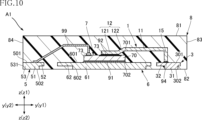
- FIG. 10 is a sectional view taken along line XX in FIG. 1.
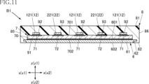
- FIG. 11 is a cross-sectional view taken along line XI-XI in FIG.
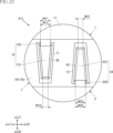
- FIG. 12 is a partially enlarged plan view showing the semiconductor device according to the first embodiment of the present disclosure.
- FIG. 13 is a partially enlarged plan view showing a first modification of the semiconductor device according to the first embodiment of the present disclosure.
- FIG. 14 is a partially enlarged plan view showing a second modification of the semiconductor device according to the first embodiment of the present disclosure.
- FIG. 15 is a partially enlarged plan view showing a third modification of the semiconductor device according to the first embodiment of the present disclosure.
- FIG. 13 is a partially enlarged plan view showing a first modification of the semiconductor device according to the first embodiment of the present disclosure.
- FIG. 14 is a partially enlarged plan view showing a second modification of the semiconductor device according to the first embodiment of the present disclosure
- FIG. 16 is a plan view showing a semiconductor device according to a second embodiment of the present disclosure.
- FIG. 17 is a cross-sectional view taken along line XVII-XVII in FIG. 16.
- FIG. 18 is a cross-sectional view taken along line XVIII-XVIII in FIG. 16.
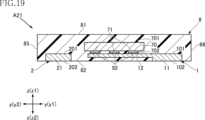
- FIG. 19 is a cross-sectional view showing a first modification of the semiconductor device according to the second embodiment of the present disclosure.
- FIG. 20 is a cross-sectional view showing a second modification of the semiconductor device according to the second embodiment of the present disclosure.
- a thing A is formed on a thing B and "a thing A is formed on a thing B” mean “a thing A is formed on a thing B” unless otherwise specified.
- "something A is placed on something B” and “something A is placed on something B” mean "something A is placed on something B” unless otherwise specified.
- a certain surface A faces (one side or the other side of) the direction B is not limited to the case where the angle of the surface A with respect to the direction B is 90 degrees; Including cases where it is tilted to the opposite direction.
- First embodiment: 1 to 12 show a semiconductor device according to a first embodiment of the present disclosure.
- the semiconductor device A1 of this embodiment includes a plurality of leads 1 to 6, a semiconductor element 7, a wire 99, and a sealing resin 8.
- the semiconductor device A1 is for switching current by being mounted on a substrate, for example, but the specific use of the semiconductor device A1 is not limited in any way.
- the thickness direction of the present disclosure is defined as the thickness direction z.
- One side in the thickness direction z is referred to as the z1 side, and the side opposite to the z1 side in the z direction is referred to as the z2 side.
- one direction perpendicular to the thickness direction z is defined as a first direction x.
- One side in the first direction x is called the x1 side, and the side opposite to the x1 side is called the x2 side.
- a direction perpendicular to the thickness direction z and the first direction x is defined as a second direction y.
- One side in the second direction y is defined as the y1 side
- the side opposite to the y1 side is defined as the y2 side.
- the plurality of leads 1 to 6 are used to appropriately achieve the function of supporting the semiconductor element 7, the function of forming a conductive path to the semiconductor element 7, and the like.
- the plurality of leads 1 to 6 are made of metal such as copper (Cu), nickel (Ni), iron (Fe), or the like.
- the plurality of leads 1 to 6 are formed, for example, by subjecting a metal plate material to a process selected from punching, bending, etching, or the like. Further, a plating layer made of silver (Ag), Ni, gold (Au), etc. may be provided at appropriate locations on each of the plurality of leads 1 to 6, if necessary.
- the plurality of leads 1 to 6 will be described as a first lead 1, a second lead 2, a third lead 3, a fourth lead 4, a fifth lead 5, and an island lead 6. That is, the plurality of leads 1 to 6 include a first lead 1, a second lead 2, a third lead 3, a fourth lead 4, a fifth lead 5, and an island lead 6. Note that, as described later, in this embodiment, the fourth lead 4 and the island lead 6 are connected to each other. Depending on the conduction form of each of the leads 1 to 6, they may be configured as separate pieces, or any of the leads may be connected to each other.
- first lead 1 and the second lead 2 are formed by punching and bending a metal plate material
- third lead 3, fourth lead 4, fifth lead 5, and island lead 6 are formed by punching and bending a metal plate material.
- An example will be explained in which a metal plate material is formed by etching.
- the island lead 6 has a main surface 601, a back surface 602, a thick part 61, a thin part 62, and a plurality of extension parts 63.
- the main surface 601 is a surface facing the z1 side in the z direction, and in the illustrated example, is a smooth surface that is perpendicular to the z direction.
- the island lead 6 may have, for example, a recess or a groove recessed from the main surface 601 as appropriate.
- the back surface 602 is a surface facing the z2 side in the z direction, and faces the opposite side to the main surface 601. In the illustrated example, back surface 602 is a smooth surface that is perpendicular to the z direction.
- a plating layer made of Ni, titanium (Ti), or the like may be provided on the back surface 602 as appropriate.
- the thick portion 61 is a portion where the main surface 601 and the back surface 602 overlap when viewed in the z direction, and in the illustrated example, is a rectangular portion when viewed in the z direction. Note that the shape of the thick portion 61 is not limited at all.
- the thickness of the thick portion 61 in the z direction is the distance between the main surface 601 and the back surface 602.
- the thin portion 62 is a portion that overlaps with the main surface 601 when viewed in the z direction but does not overlap with the back surface 602. In the illustrated example, the thin portion 62 extends from the thick portion 61 to both sides in the x direction and both sides in the y direction when viewed in the z direction. It is connected in such a way that it extends to.
- the thickness of the thin portion 62 in the z direction is smaller than the distance between the main surface 601 and the back surface 602.
- the thickness of the thick portion 61 and the thickness of the thin portion 62 are not limited at all.
- the thickness of the thick portion 61 is approximately 0.2 mm to 0.5 mm
- the thickness of the thin portion 62 is approximately 0.1 mm to 0.4 mm.
- the portion of the thin portion 62 that extends from the thick portion 61 toward the y1 side in the y direction is larger than the portion that extends toward the y2 side.
- the plurality of extending portions 63 are portions extending from the end of the thin wall portion 62. In the illustrated example, the plurality of extending portions 63 extend from the thin portion 62 to both sides in the x direction.
- the number of extension parts 63 is not limited at all, and may be plural or one. In the illustrated example, two extending portions 63 are provided on the x1 side in the x direction, and two extending portions 63 are provided on the x2 side.
- the extending portion 63 has an end surface 631.
- the end surface 631 is a surface facing away from the thin wall portion 62 in the x direction, in other words, a surface facing outward in the x direction.
- the illustrated end surface 631 is a surface perpendicular to the x direction.
- the positions in the x direction of the two end surfaces 631 located on the x1 side in the x direction are the same (or substantially the same). Moreover, the positions in the x direction of the two end surfaces 631 located on the x2 side in the x direction are the same (or substantially the same).
- the first lead 1 As shown in FIGS. 1, 7, and 8 to 12, the first lead 1 is arranged on the z1 side in the z direction relative to the third lead 3, fourth lead 4, fifth lead 5, and island lead 6. ing.
- the first lead 1 of this embodiment includes a first main portion 11 , a plurality of first branch portions 12 , a first extension portion 13 , a third extension portion 14 , and a first standing portion 15 .
- the first main portion 11 is a plate-shaped portion along the xy plane, and in the illustrated example, has a substantially rectangular shape with the x direction as the longitudinal direction.
- the first main portion 11 in the illustrated example has a through hole 111 .
- the through hole 111 penetrates the first main portion 11 in the z direction.
- the number of through holes 111 is not limited, and may be one or more.
- the first main portion 11 has two through holes 111.
- the shape of the through hole 111 is not limited at all, and a circular shape, an elliptical shape, a rectangular shape, a polygonal shape, etc. are appropriately selected.
- the through hole 111 has an elliptical shape with the x direction as the longitudinal direction when viewed in the z direction.
- the plurality of first branch parts 12 extend from the first main part 11 to the y2 side in the y direction.
- the number of first branch parts 12 is not limited at all, and in the illustrated example, three first branch parts 12 are provided.
- the plurality of first branch parts 12 are arranged side by side in the x direction.
- the first branch portion 12 has a first connecting portion 121 and a first root portion 122 .
- the first connecting portion 121 is a portion located on the y2 side in the y direction with respect to the first main portion 11.
- the first connecting portion 121 is located closer to the z2 side than the first main portion 11 in the z direction.
- the shape of the first connecting portion 121 is not limited at all, and in the illustrated example, it has a shape whose longitudinal direction is the y direction when viewed in the z direction.
- the first connection portion 121 is perpendicular to the z direction.
- the first root portion 122 is located between the first connecting portion 121 and the first main portion 11 and is connected to the first connecting portion 121 and the first main portion 11.
- the first root portion 122 approaches the semiconductor element 7 in the z direction (located on the z2 side) as it goes from the first main portion 11 to the first connection portion 121 in the y direction (from the y1 side to the y2 side). is inclined to.
- the three first branch portions 12 include first branch portions 12 that have different lengths in the y direction.
- the first branch 12 located closest to the x2 side in the x direction has a shorter length in the y direction than the other first branches 12.
- the first branch portion 12 located closest to the x2 side in the x direction is located close to a third electrode 73 and a wire 99, which will be described later.
- the plurality of first branch parts 12 may have the same length.
- the first width W11 which is the width in the first direction It is narrower than the second width W12, which is the width in the first direction x.
- the first connecting portion 121 of this example has a shape in which the width in the first direction x decreases from the tip on the y2 side toward the first root portion 122 in the y direction. This first connecting portion 121 is configured only by the first tapered portion of the present disclosure.
- the third width W13 which is the width in the first direction x of the boundary between the first root portion 122 and the first connection portion 121, is smaller than the second width W12.
- the width of the first root portion 122 in the first direction x increases from the first connecting portion 121 side (y2 side) to the first main portion 11 side (y1 side) in the y direction. It has a tapered shape that increases in size.
- the first branch portion 12 in the illustrated example has a tapered shape in which the width in the first direction x increases as it goes from the y2 side to the y1 side in the y direction. That is, the first connecting portion 121 and the first root portion 122 have a continuous tapered shape when viewed in the z direction.
- the first extending portion 13 is a portion extending from the first main portion 11.
- the first extending portion 13 extends from the end of the first main portion 11 on the x1 side in the x direction toward the x1 side.
- the first extending portion 13 has a first end surface 131 .
- the first end surface 131 is a surface facing the opposite side from the first main portion 11 in the x direction, in other words, a surface facing the x1 side which is the outside in the x direction.
- the illustrated first end surface 131 is a surface perpendicular to the x direction.
- the position of the first end surface 131 in the x direction is the same (or substantially the same) as the position in the x direction of the plurality of end surfaces 631 located on the x1 side in the x direction.
- the third extending portion 14 is a portion extending from the first main portion 11.
- the third extending portion 14 extends from the end of the first main portion 11 on the x2 side in the x direction toward the x2 side.
- the third extending portion 14 has a third end surface 141.
- the third end surface 141 is a surface facing the opposite side from the first main portion 11 in the x direction, in other words, a surface facing the x2 side which is the outside in the x direction.
- the illustrated third end surface 141 is a surface perpendicular to the x direction. Further, the position of the third end surface 141 in the x direction is the same (or substantially the same) as the position in the x direction of the plurality of end surfaces 631 located on the x2 side in the x direction.
- the first standing portion 15 is connected to an end portion of the first main portion 11 on the y1 side in the y direction, which is opposite to the first branch portion 12.
- the first upright portion 15 extends from the first main portion 11 toward the z2 side in the z direction.
- the shape of the first upright portion 15 is not limited in any way, and in the illustrated example, it has a rectangular shape with the x direction as the longitudinal direction. In the illustrated example, the center of the first upright portion 15 in the x direction is the same (or substantially the same) as the center of the first main portion 11 in the x direction.
- the z2 side tip of the first upright portion 15 of the first lead 1 in the z direction is electrically connected to the third lead 3 via the fourth conductive joint 94.
- the fourth conductive joint 94 is made of, for example, solder, Ag paste material, Ag sintered material, Cu sintered material, or the like.
- 2nd lead 2 As shown in FIGS. 1, 7, and 8 to 12, the second lead 2 is arranged on the z1 side in the z direction relative to the third lead 3, fourth lead 4, fifth lead 5, and island lead 6. ing. Further, the second lead 2 is arranged on the y2 side in the y direction with respect to the first lead 1.
- the second lead 2 of this embodiment includes a second main portion 21, a plurality of second branch portions 22, a second extension portion 23, a fourth extension portion 24, a second upright portion 25, and a connecting portion 29. are doing.
- the second main portion 21 is a plate-shaped portion along the xy plane, and in the illustrated example, has a substantially rectangular shape with the x direction as the longitudinal direction.
- the first main portion 11 and the second main portion 21 are arranged on opposite sides of each other in the y direction with the semiconductor element 7 as a reference.
- the second main portion 21 in the illustrated example has a through hole 211 .
- the through hole 211 penetrates the second main portion 21 in the z direction.
- the number of through holes 211 is not limited, and may be one or more.
- the second main portion 21 has two through holes 211 .
- the shape of the through hole 211 is not limited at all, and a circular shape, an elliptical shape, a rectangular shape, a polygonal shape, etc.
- the through hole 211 has an elliptical shape with the x direction as the longitudinal direction when viewed in the z direction.
- the second main part 21 is arranged at the same (or substantially the same) position as the first main part 11 in the z direction.
- the plurality of second branch portions 22 extend from the second main portion 21 toward the y1 side in the y direction.
- the number of second branch parts 22 is not limited at all, and in the illustrated example, two second branch parts 22 are provided.
- the plurality of second branch parts 22 are arranged side by side in the x direction.
- the second branch portion 22 has a second connecting portion 221 and a second root portion 222 .
- the second connecting portion 221 is a portion located on the y1 side in the y direction with respect to the second main portion 21.
- the second connecting portion 221 is located closer to the z2 side than the second main portion 21 in the z direction.
- the shape of the second connecting portion 221 is not limited at all, and in the illustrated example, it has a shape whose longitudinal direction is the y direction when viewed in the z direction.
- the second connection portion 221 is perpendicular to the z direction.
- the second root portion 222 is located between the second connection portion 221 and the second main portion 21 and is connected to the second connection portion 221 and the second main portion 21 .
- the second root portion 222 approaches the semiconductor element 7 in the z direction (located on the z2 side) as it goes from the second main portion 21 to the second connection portion 221 in the y direction (as it goes from the y2 side to the y1 side). is inclined to.
- the lengths of the two second branch portions 22 in the y direction are equal.
- the plurality of second branch portions 22 may have different lengths in the y direction.
- the fourth width W21 which is the width in the first direction It is narrower than the fifth width W22, which is the width in the first direction x.
- the second connecting portion 221 of this example has a shape in which the width in the first direction x decreases from the tip on the y1 side toward the second root portion 222 in the y direction. This second connecting portion 221 is configured only by the second tapered portion of the present disclosure.
- the sixth width W23 which is the width in the first direction x of the boundary between the second root portion 222 and the second connecting portion 221, is smaller than the fifth width W22.
- the width of the second root portion 222 in the first direction x increases from the second connecting portion 221 side (y1 side) to the second main portion 21 side (y2 side) in the y direction. It has a tapered shape that increases in size.
- the second branch portion 22 in the illustrated example has a tapered shape in which the width in the first direction x increases as it goes from the y1 side to the y2 side in the y direction. That is, the second connecting portion 221 and the second root portion 222 have a continuous tapered shape when viewed in the z direction.
- the second extending portion 23 is a portion extending from the second main portion 21.
- the second extending portion 23 extends from the end of the second main portion 21 on the x1 side in the x direction toward the x1 side.
- the second extending portion 23 has a second end surface 231 .
- the second end surface 231 is a surface facing the opposite side from the second main portion 21 in the x direction, in other words, a surface facing the x1 side which is the outside in the x direction.
- the illustrated second end surface 231 is a surface perpendicular to the x direction.
- the position of the second end surface 231 in the x direction is the same (or substantially the same) as the first end surface 131 and the end surface 631 located on the x1 side in the x direction.
- the fourth extending portion 24 is connected to the second main portion 21 via a connecting portion 29.
- the connecting portion 29 has a smaller dimension in the y direction than the second main portion 21 and the fourth extending portion 24 .
- the fourth extending portion 24 in the present disclosure is not limited to a configuration in which it is directly connected to the second main portion 21, but includes a configuration in which it is connected to the second main portion 21 via another portion. The same applies to the second extending portion 23 in this respect.
- the above-mentioned first extension part 13 and third extension part 14 are not limited to a structure in which they are directly connected to the first main part 11, but are also in a structure in which they are connected to the first main part 11 through other parts. including.
- the fourth extending portion 24 extends along the y direction.
- the fourth extending portion 24 has a fourth end surface 241 .
- the fourth end surface 241 is a surface facing opposite to the second main portion 21 in the y direction, in other words, a surface facing the y2 side, which is the outside in the y direction.
- the illustrated fourth end surface 241 is a surface perpendicular to the y direction.
- the second upright portion 25 is connected to the end of the second main portion 21 on the y2 side in the y direction, which is opposite to the second branch portion 22.
- the second upright portion 25 extends from the second main portion 21 toward the z2 side in the z direction.
- the shape of the second upright portion 25 is not limited at all, and in the illustrated example, it has a rectangular shape with the x direction as the longitudinal direction. In the illustrated example, the center of the second upright portion 25 in the x direction is the same (or substantially the same) as the center of the second main portion 21 in the x direction.
- the tip of the second upright portion 25 of the second lead 2 on the z2 side in the z direction is electrically connected to the fourth lead 4 via the fifth conductive joint 95.
- the fifth conductive joint 95 is, for example, solder.
- the third lead 3 is arranged apart from the island lead 6 on the y1 side in the y direction.
- the center of the third lead 3 in the x direction is the same (or substantially the same) as the center of the island lead 6 in the x direction.
- the third lead 3 has a main surface 301, a back surface 302, a thick part 31, a thin part 32, and a plurality of extension parts 33.
- the main surface 301 is a surface facing the z1 side in the z direction, and in the illustrated example, is a smooth surface that is perpendicular to the z direction.
- the third lead 3 may have, for example, a recess or a groove recessed from the main surface 301 as appropriate.
- the first upright portion 15 described above is joined to the main surface 301 via the fourth conductive joint 94 .
- the back surface 302 is a surface facing the z2 side in the z direction, and faces the opposite side to the main surface 301.
- back surface 302 is a smooth surface that is perpendicular to the z direction.
- a plating layer made of Ni, Ti, etc. may be provided on the back surface 302 as appropriate.
- the main surface 301 is at the same (or substantially the same) position as the main surface 601 in the z direction
- the back surface 302 is at the same (or substantially the same) position as the back surface 602.
- the thick portion 31 is a portion where the main surface 301 and the back surface 302 overlap when viewed in the z direction.
- the thick portion 31 is a rectangular portion whose longitudinal direction is the x direction when viewed in the z direction. Note that the shape of the thick portion 31 is not limited at all.
- the thickness of the thick portion 31 in the z direction is the distance between the main surface 301 and the back surface 302.
- the thin portion 32 is a portion that overlaps the main surface 301 and does not overlap the back surface 302 when viewed in the z direction.
- the thin portion 32 is connected to the thick portion 31 so as to extend from the thick portion 31 to both sides in the x direction and to the y2 side in the y direction.
- the thin portion 32 has a portion connected to the thick portion 31 so as to extend toward the y1 side in the y direction when viewed in the z direction, and this portion is sandwiched between the extending portions 33 in the x direction.
- the thickness of the thin portion 32 in the z direction is smaller than the distance between the main surface 301 and the back surface 302.
- the thickness of the thick portion 31 and the thickness of the thin portion 32 are not limited at all. In this embodiment, the thickness of the thick portion 31 is the same (or approximately the same) as the thickness of the thick portion 61, and the thickness of the thin portion 32 is the same (or approximately the same) as the thickness of the thin portion 62. ).
- the plurality of extending portions 33 are portions extending from the end of the thick portion 31. In the illustrated example, the plurality of extending portions 33 extend from the thick portion 31 toward the y1 side in the y direction.
- the number of extension parts 33 is not limited at all, and may be plural or one. In the illustrated example, four extensions 33 are provided.
- the extending portion 33 has an end surface 331.
- the end surface 331 is a surface facing the opposite side from the thick portion 31 in the y direction, in other words, a surface facing the y1 side, which is the outside in the y direction.
- the illustrated end surface 331 is a surface perpendicular to the y direction. The positions of the plurality of end surfaces 331 in the y direction are the same (or substantially the same).
- the fourth lead 4 is arranged on the y2 side of the island lead 6 in the y direction. Further, the center of the fourth lead 4 in the x direction is located on the x1 side in the x direction from the center of the island lead 6 in the x direction. In the semiconductor device A1, the fourth lead 4 and the island lead 6 are connected by a relay portion 49. Unlike this configuration, the fourth lead 4 may be separated from the island lead 6. As shown in FIGS. 1 to 3 and 8 to 10, the fourth lead 4 has a main surface 401, a back surface 402, a thick part 41, a thin part 42, and a plurality of extension parts 43.
- the main surface 401 is a surface facing the z1 side in the z direction, and in the illustrated example, is a smooth surface that is perpendicular to the z direction.
- the fourth lead 4 may have, for example, a recess or a groove recessed from the main surface 401 as appropriate.
- the aforementioned second standing portion 25 is joined to the main surface 401 via the fifth conductive joining portion 95 .
- the back surface 402 is a surface facing the z2 side in the z direction, and faces the opposite side to the main surface 401.
- back surface 402 is a smooth surface that is perpendicular to the z direction.
- a plating layer made of Ni, Ti, etc. may be provided on the back surface 402 as appropriate.
- the main surface 401 is at the same (or substantially the same) position as the main surface 601 in the z direction
- the back surface 402 is at the same (or substantially the same) position as the back surface 602.
- the thick portion 41 is a portion where the main surface 401 and the back surface 402 overlap when viewed in the z direction.
- the thick portion 41 is a rectangular portion whose longitudinal direction is the x direction when viewed in the z direction. Note that the shape of the thick portion 41 is not limited at all.
- the thickness of the thick portion 41 in the z direction is the distance between the main surface 401 and the back surface 402. In this embodiment, the dimension of the thick portion 41 in the x direction is smaller than the dimension of the thick portion 31 in the x direction.
- the thin portion 42 is a portion that overlaps the main surface 401 and does not overlap the back surface 402 when viewed in the z direction.
- the thin portion 42 is connected to the thick portion 41 so as to extend from the thick portion 41 to both sides in the x direction and to the y1 side in the y direction. Further, the thin wall portion 42 has a portion extending from the thick wall portion 41 toward the y2 side in the y direction when viewed in the z direction, and this portion is sandwiched between the extending portions 43 in the x direction.
- the thickness of the thin portion 42 in the z direction is smaller than the distance between the main surface 401 and the back surface 402.
- the thickness of the thick portion 41 and the thickness of the thin portion 42 are not limited at all. In this embodiment, the thickness of the thick portion 41 is the same (or approximately the same) as the thickness of the thick portion 61, and the thickness of the thin portion 42 is the same (or approximately the same) as the thickness of the thin portion 62. ).
- the plurality of extending portions 43 are portions extending from the end of the thick portion 41.
- the plurality of extending portions 43 extend from the thick portion 41 toward the y2 side in the y direction.
- the number of extension parts 43 is not limited at all, and may be plural or one.
- three extensions 43 are provided. The positions of these three extensions 43 in the x direction are the same (or approximately the same) as the positions in the x direction of the three extensions 33 located on the x1 side in the x direction among the plurality of extensions 33. .
- the extending portion 43 has an end surface 431.
- the end surface 431 is a surface facing away from the thick portion 41 in the y direction, in other words, a surface facing the y2 side, which is the outside in the y direction.
- the illustrated end surface 431 is a surface perpendicular to the y direction.
- the positions of the plurality of end surfaces 431 in the y direction are the same (or substantially the same). Further, the positions of the plurality of end surfaces 431 in the y direction are the same (or substantially the same) as the fourth end surface 241.
- the fifth lead 5 is arranged on the y2 side of the island lead 6 in the y direction. Further, the center of the fifth lead 5 in the x direction is located on the x2 side in the x direction from the center of the island lead 6 in the x direction. The fifth lead 5 is arranged on the x2 side in the x direction with respect to the fourth lead 4. As shown in FIGS. 1 to 3 and FIG. 10, the fifth lead 5 has a main surface 501, a back surface 502, a thick portion 51, a thin portion 52, and an extending portion 53.
- the main surface 501 is a surface facing the z1 side in the z direction, and in the illustrated example, is a smooth surface that is perpendicular to the z direction.
- the fifth lead 5 may have, for example, a recess or a groove recessed from the main surface 501 as appropriate.
- a wire 99 is bonded to the main surface 501 .
- the back surface 502 is a surface facing the z2 side in the z direction, and faces the opposite side to the main surface 501.
- back surface 502 is a smooth surface that is perpendicular to the z direction.
- a plating layer made of Ni, Ti, etc. may be provided on the back surface 502 as appropriate.
- the main surface 501 is at the same (or substantially the same) position as the main surface 601 in the z direction
- the back surface 502 is at the same (or substantially the same) position as the back surface 602.
- the thick portion 51 is a portion where the main surface 501 and the back surface 502 overlap when viewed in the z direction.
- the thick portion 51 is a rectangular portion when viewed in the z direction.
- the shape of the thick portion 51 is not limited at all.
- the thickness of the thick portion 51 in the z direction is the distance between the main surface 501 and the back surface 502.
- the dimension of the thick portion 51 in the x direction is smaller than the dimension of the thick portion 31 and the thick portion 41 in the x direction.
- the thin portion 32 is a portion that overlaps the main surface 301 and does not overlap the back surface 302 when viewed in the z direction.
- the thin portion 32 is connected to the thick portion 51 so as to extend from the thick portion 51 to both sides in the x direction and to the y1 side in the y direction.
- the thickness of the thin portion 52 in the z direction is smaller than the distance between the main surface 501 and the back surface 502.
- the thickness of the thick portion 51 and the thickness of the thin portion 52 are not limited at all. In this embodiment, the thickness of the thick portion 51 is the same (or approximately the same) as the thickness of the thick portion 61, and the thickness of the thin portion 52 is the same (or approximately the same) as the thickness of the thin portion 62. ).
- the extending portion 53 is a portion extending from the end of the thick portion 51. In the illustrated example, the extending portion 53 extends from the thick portion 51 toward the y2 side in the y direction.
- the number of extension parts 53 is not limited at all, and may be plural or one. In the illustrated example, one extension 53 is provided.
- the position of the extension part 53 in the x direction is the same (or substantially the same) as the position in the x direction of the extension part 33 located closest to the x2 side in the x direction among the plurality of extension parts 33.
- the extending portion 53 has an end surface 531.
- the end surface 531 is a surface facing opposite to the thick portion 51 in the y direction, in other words, a surface facing the y2 side, which is the outside in the y direction.
- the illustrated end surface 531 is a surface perpendicular to the y direction. Further, the position of the end surface 531 in the y direction is the same (or substantially the same) as the fourth end surface 241 and the plurality of end surfaces 431.
- the semiconductor element 7 is an element that performs the electrical functions of the semiconductor device A1.
- the specific configuration of the semiconductor element 7 is not limited at all, and in this embodiment, the semiconductor element 7 is a transistor using a nitride semiconductor, and more specifically, a GaN-transistor using gallium nitride (GaN). It is a HEMT (High Electron Mobility Transistor) element.
- the semiconductor element 7 is not limited to one using a nitride semiconductor, and may also use other semiconductors such as silicon (Si) and silicon carbide (SiC).
- the semiconductor element 7 is not limited to a HEMT, and may be other transistors such as a MOSFET (Metal-Oxide-Semiconductor Field Effect Transistor) and an IGBT (Insulated Gate Bipolar Transistor).
- MOSFET Metal-Oxide-Semiconductor Field Effect Transistor
- IGBT Insulated Gate Bipolar Transistor
- the semiconductor element 7 is mounted on the thick portion 61 of the island lead 6. As shown in FIGS. 1, 2, and 8 to 12, the semiconductor element 7 includes an element body 70, a plurality of first electrodes 71, a plurality of second electrodes 72, and a third electrode 73.
- the element body 70 is, for example, a portion in which a substrate layer, a buffer layer, and a nitride layer (all not shown) are laminated.
- the element body 70 has an element main surface 701 and an element back surface 702.
- the element main surface 701 is a surface facing the z1 side in the z direction.
- the element back surface 702 is a surface facing the z2 side in the z direction, and faces the opposite side to the element main surface 701.
- the back surface 702 of the element is provided with a metal layer. As shown in FIGS. 12 to 14, this metal layer and the main surface 601 of the island lead 6 are joined by a first conductive joint 91. As shown in FIGS.
- the first conductive joint 91 is made of, for example, solder, Ag paste material, Ag sintered material, Cu sintered material, or the like.
- the above-described metal layer is provided for bonding by the first conductive bonding portion 91, a configuration may be adopted in which the metal layer is not provided.
- the metal layer may have the same potential as, for example, the second electrode 72 and the like.
- the semiconductor element 7 is disposed at a position overlapping a portion of the thick portion 61 and a portion of the thin portion 62 of the island lead 6 when viewed in the z direction.
- a plurality of first electrodes 71, a plurality of second electrodes 72, and a third electrode 73 are arranged on the element main surface 701.
- the numbers of the plurality of first electrodes 71 and the plurality of second electrodes 72 are not limited at all. In the illustrated example, three first electrodes 71 and two second electrodes 72 are provided.
- the number of the plurality of first electrodes 71 and the number of the plurality of first branch parts 12 are the same, and the number of the plurality of second electrodes 72 and the number of the plurality of second branch parts 22 are the same.
- the first electrode 71 is an electrode that functions as a drain electrode.
- the second electrode 72 is an electrode that functions as a source electrode.
- the plurality of first electrodes 71 and the plurality of second electrodes 72 are arranged alternately in the x direction.
- the shapes of the first electrode 71 and the second electrode 72 are not limited at all, and in the illustrated example, they have a shape whose longitudinal direction is in the y direction, and more specifically, a tapered shape.
- FIG. 1, FIG. 2, FIG. 8, and FIGS. They are individually electrically connected via conductive joints 92 .
- the second conductive joint 92 is made of, for example, solder, Ag paste material, Ag sintered material, Cu sintered material, or the like.
- FIG. 1, FIG. 2, FIG. 9, FIG. 11, and FIG. They are individually electrically connected via conductive joints 93.
- the third conductive joint 93 is made of, for example, solder, Ag paste material, Ag sintered material, Cu sintered material, or the like.
- the third electrode 73 is an electrode that functions as a gate electrode.
- the number of third electrodes 73 is not limited, and may be one or more. In the illustrated example, one third electrode 73 is provided.
- the third electrode 73 is arranged, for example, at one of the four corners of the element main surface 701, and in the illustrated example, it is arranged near the corner of the element main surface 701 on the x2 side in the x direction and the y2 side in the y direction. has been done. Further, the third electrode 73 is arranged on the y2 side in the y direction with respect to the first electrode 71 on the x2 side in the x direction of the two first electrodes 71.
- a wire 99 is connected to the third electrode 73 and electrically connected to the fifth lead 5 via the wire 99. Note that instead of the wire 99, a conductive member made of a metal plate material may be used to conduct the third electrode 73 and the fifth lead 5.
- the sealing resin 8 covers a portion of each of the plurality of leads 1 to 6, the semiconductor element 7, and the wire 99, and is made of an insulating material such as epoxy resin. As shown in FIGS. 1 to 11, the sealing resin 8 has a first surface 81, a second surface 82, a third surface 83, a fourth surface 84, a fifth surface 85, and a sixth surface 86. , has a rectangular parallelepiped shape.
- the first surface 81 is a surface facing the z1 side in the z direction. In the illustrated example, the first surface 81 is a plane perpendicular to the z direction.
- the second surface 82 is a surface facing the z2 side in the z direction. In the illustrated example, the second surface 82 is a plane perpendicular to the z direction.
- the third surface 83 is a surface facing the y1 side in the y direction. In the illustrated example, the third surface 83 is a plane perpendicular to the y direction.
- the fourth surface 84 is a surface facing the y2 side in the y direction. In the illustrated example, the fourth surface 84 is a plane perpendicular to the y direction.
- the fifth surface 85 is a surface facing the x1 side in the x direction. In the illustrated example, the fifth surface 85 is a plane perpendicular to the x direction.
- the sixth surface 86 is a surface facing the x2 side in the x direction. In the illustrated example, the sixth surface 86 is a plane perpendicular to the x direction.
- the back surface 602 of the island lead 6, the back surface 302 of the third lead 3, the back surface 402 of the fourth lead 4, and the back surface 502 of the fifth lead 5 are exposed on the z2 side in the z direction.
- the second surface 82, the back surface 602 of the island lead 6, the back surface 302 of the third lead 3, the back surface 402 of the fourth lead 4, and the back surface 502 of the fifth lead 5 are flush with each other.
- all or any of the back surface 602 of the island lead 6, the back surface 302 of the third lead 3, the back surface 402 of the fourth lead 4, and the back surface 502 of the fifth lead 5 may protrude slightly from the second surface 82. good.
- a plurality of end surfaces 331 of the third lead 3 are exposed on the y1 side in the y direction.
- the third surface 83 and the plurality of end surfaces 331 of the third lead 3 are flush with each other. However, all or any of the plurality of end surfaces 331 may slightly protrude from the third surface 83.
- the fourth end surface 241 of the second lead 2, the plurality of end surfaces 431 of the fourth lead 4, and the end surface 531 of the fifth lead 5 are exposed on the y2 side in the y direction.
- the fourth surface 84, the fourth end surface 241 of the second lead 2, the plurality of end surfaces 431 of the fourth lead 4, and the end surface 531 of the fifth lead 5 are flush with each other.
- all or any of the fourth end surface 241 of the second lead 2, the plurality of end surfaces 431 of the fourth lead 4, and the end surface 531 of the fifth lead 5 may protrude slightly from the fourth surface 84.
- the first end surface 131 of the first lead 1, the second end surface 231 of the second lead 2, and the plurality of end surfaces 631 of the island lead 6 are exposed on the x1 side in the x direction.
- the fifth surface 85, the first end surface 131 of the first lead 1, the second end surface 231 of the second lead 2, and the plurality of end surfaces 631 of the island lead 6 are flush with each other. However, all or any of the first end surface 131 of the first lead 1, the second end surface 231 of the second lead 2, and the plurality of end surfaces 631 of the island lead 6 may protrude slightly from the fifth surface 85.
- the third end surface 141 of the first lead 1 and the plurality of end surfaces 631 of the island leads 6 are exposed on the x2 side in the x direction.
- the sixth surface 86, the third end surface 141 of the first lead 1, and the plurality of end surfaces 631 of the island lead 6 are flush with each other.
- all or any of the third end surface 141 of the first lead 1 and the plurality of end surfaces 631 of the island lead 6 may protrude slightly from the sixth surface 86.
- the semiconductor device A1 is mounted on a circuit board (not shown) or the like using the back surface 302, back surface 402, and back surface 502 exposed from the second surface 82 of the sealing resin 8 as mounting terminals. That is, in the semiconductor device A1, the mounting surface is the z2 side opposite to the z1 side, which is the side toward which the element main surface 701 of the semiconductor element 7 faces in the z direction. Further, the back surface 602 is used as a heat dissipation surface for dissipating heat from the semiconductor element 7.
- the first width W11 of the first branch portion 12 is narrower than the second width W12.
- the first connecting portion 121 is electrically connected to the first electrode 71 . Therefore, a current flows in the first branch portion 12 in the y direction. This current increases toward the first main portion 11 in the y direction.
- the first branch portion 12, which is a current conduction path, has a larger width on the side where the first main portion 11 is located in the y direction. Therefore, current concentration on the current path can be alleviated.
- the first branch portion 12 is in a cantilevered state with one side supported by the first main portion 11.
- the tip of the first branch part 12 is positioned on the z2 side in the thickness direction z.
- the entire first branch portion 12 may bend.
- the second width W12 is larger than the first width W11, it is possible to suppress the bending of the first branch portion 12, and it is possible to more appropriately manufacture the semiconductor device A1. .
- the first connecting portion 121 has a tapered shape in which the width in the first direction x increases toward the first root portion 122 in the y direction. Such a shape is preferable for alleviating current concentration. Further, in this example, the entire first connecting portion 121 has a tapered shape. Such a configuration is preferable because it alleviates current concentration.
- the first root portion 122 has a tapered shape. This can further promote mitigation of current concentration and suppression of deflection.
- the fourth width W21 of the second branch portion 22 is narrower than the fifth width W22.
- the second connection portion 221 is electrically connected to the second electrode 72 . Therefore, a current flows in the second branch portion 22 in the y direction. This current increases toward the first main portion 11 in the y direction.
- the second branch portion 22, which is the current conduction path has a larger width on the side where the first main portion 11 is located in the y direction. Therefore, current concentration on the current path can be alleviated.
- the second branch portion 22 is in a cantilevered state with one side supported by the first main portion 11.
- the tip of the second branch portion 22 is positioned on the z2 side in the thickness direction z.
- the entire second branch portion 22 may bend.
- the fifth width W22 is larger than the fourth width W21, it is possible to suppress the bending of the second branch portion 22, and the semiconductor device A1 can be manufactured more appropriately. .
- the second connecting portion 221 has a tapered shape in which the width in the first direction x increases toward the first root portion 122 in the y direction. Such a shape is preferable for alleviating current concentration. Further, in this example, the entire second connecting portion 221 has a tapered shape. Such a configuration is preferable because it alleviates current concentration.
- first root portion 122 has a tapered shape. This can further promote mitigation of current concentration and suppression of deflection.
- FIG. 13 shows a first modification of the semiconductor device A1.
- the configurations of the first branch portion 12 and the second branch portion 22 are different from the semiconductor device A1.
- the second width W12 and the third width W13 of the first branch portion 12 are equal. That is, the first root portion 122 has a shape with a constant width in the first direction x. Further, the fifth width W22 and the sixth width W23 of the second branch portion 22 are equal. That is, the second root portion 222 has a shape with a constant width in the first direction x.
- the first branch portion 12 and the first extension portion 13 are not limited to a tapered configuration as a whole.
- FIG. 14 shows a second modification of the semiconductor device A1.
- the configurations of the first branch portion 12 and the second branch portion 22 are different from those of the above-mentioned example.
- first root portion 122 and the second root portion 222 both have a shape with a constant width in the first direction x.
- the first connecting portion 121 includes a first tapered portion 1211 and a first equal width portion 1212.
- the first tapered portion 1211 has a shape in which the width in the first direction x increases from the tip on the y2 side toward the first root portion 122 side (y1 side).
- the first equal width portion 1212 is interposed between the first tapered portion 1211 and the first root portion 122.
- the first equal width portion 1212 has a constant width in the first direction x. In the illustrated example, the width of the first equal width portion 1212 in the first direction x is the same as (or approximately equal to) the width of the first root portion 122 in the first direction same).
- the first length L11 which is the length of the first tapered part 1211 in the y direction, is longer than the second length L12, which is the length of the first equal width part 1212 in the y direction.
- the second connecting portion 221 includes a second tapered portion 2211 and a second equal width portion 2212.
- the second tapered portion 2211 has a shape in which the width in the first direction x increases from the tip on the y1 side toward the second root portion 222 side (y2 side).
- the second equal width portion 2212 is interposed between the second tapered portion 2211 and the second root portion 222.
- the second equal width portion 2212 has a constant width in the first direction x.
- the width of the second equal width portion 2212 in the first direction x is the same as (or approximately) the width of the second root portion 222 in the first direction same).
- the third length L21 which is the length of the second tapered portion 2211 in the y direction, is longer than the fourth length L22, which is the length of the second equal width portion 2212 in the y direction.
- the first connecting portion 121 and the first root portion 122 are not limited to a configuration consisting only of a tapered portion.
- FIG. 15 shows a third modification of the semiconductor device A1.
- the configurations of the first branch portion 12 and the second branch portion 22 are different from those of the above-mentioned example.
- the first root portion 122 of this modification includes a first wide portion 1221 and a second narrow portion 1222.
- the first wide portion 1221 has a larger width in the first direction x than the second narrow portion 1222 and is interposed between the second narrow portion 1222 and the first main portion 11 .
- the second narrow portion 1222 is interposed between the first wide portion 1221 and the first connecting portion 121 .
- the width of the first wide portion 1221 in the first direction x is the second width W12
- the width of the second narrow portion 1222 in the first direction x is the third width W13. There is.
- the first wide portion 1221 does not overlap the first electrode 71 when viewed in the thickness direction z.
- the second root portion 222 of this modification includes a first wide portion 2221 and a second narrow portion 2222.
- the first wide portion 2221 has a larger width in the first direction x than the second narrow portion 2222 and is interposed between the second narrow portion 2222 and the second main portion 21 .
- the second narrow portion 2222 is interposed between the first wide portion 2221 and the second connecting portion 221.
- the width of the first wide portion 2221 in the first direction x is the fifth width W22
- the width of the second narrow portion 2222 in the first direction x is the sixth width W23.
- the first wide portion 2221 does not overlap the second electrode 72 when viewed in the thickness direction z.
- the shapes of the first root portion 122 and the second root portion 222 are not limited at all.
- the first wide part 1221 does not overlap with the first electrode 71 and the first wide part 2221 does not overlap with the second electrode 72 when viewed in the thickness direction z, the first wide part 1221 and the first wide part 1221 do not overlap with the second electrode 72. Insulation between the first electrode 71 and the first wide portion 2221 and the second electrode 72 can be more reliably ensured.
- Second embodiment 16 to 18 show a semiconductor device according to a second embodiment of the present disclosure.
- the semiconductor device A2 of this embodiment includes a first lead 1, a second lead 2, a fifth lead 5, a semiconductor element 7, and a sealing resin 8.
- the semiconductor element 7 of this embodiment is arranged with the element main surface 701 facing the z2 side in the z direction and the element back surface 702 facing the z1 side in the z direction.
- the plurality of first electrodes 71, the plurality of second electrodes 72, and the third electrodes 73 are constituted by a plurality of metal bumps.
- the plurality of first electrodes 71 are made up of a plurality of metal bumps (two or three in the figure) arranged in the y direction.
- a plurality of sets (three sets) of first electrodes 71 are arranged in the first direction x.
- the plurality of second electrodes 72 are made up of a plurality of metal bumps (three in the figure) arranged in the y direction.
- a plurality of sets (two sets) of second electrodes 72 are arranged in the first direction x.
- the plurality of sets of first electrodes 71 and the plurality of sets of second electrodes 72 are arranged alternately in the first direction x.
- the first lead 1 has a main surface 101 and a back surface 102.
- the main surface 101 is a surface facing the z1 side in the z direction, and faces the element main surface 701 of the semiconductor element 7 .
- the back surface 102 is a surface facing the z2 side in the z direction, and is exposed from the second surface 82 of the sealing resin 8.
- the thickness of the first lead 1 in the z direction is constant.
- the second lead 2 has a main surface 201 and a back surface 202.
- the main surface 201 is a surface facing the z1 side in the z direction, and faces the element main surface 701 of the semiconductor element 7 .
- the back surface 202 is a surface facing the z2 side in the z direction, and is exposed from the second surface 82 of the sealing resin 8.
- the thickness of the second lead 2 in the z direction is constant.
- the shapes of the plurality of first branch portions 12 of the first lead 1 and the plurality of second branch portions 22 of the second lead 2 when viewed in the z direction are, for example, similar to the plurality of first branch portions 12 and the plurality of second branch portions 22 of the semiconductor device A1 described above. This is similar to the second branch 22 of.
- the plurality of first branch parts 12 and the plurality of second branch parts 22 may have the shapes in the semiconductor devices A11, A12, A13, or may have other shapes.
- the plurality of first branch parts 12 and the plurality of second branch parts 22 are located on the z2 side in the z direction with respect to the semiconductor element 7.
- the plurality of first branch parts 12 are individually electrically connected to the plurality of sets of first electrodes 71 via second conductive joints 92.
- the plurality of second branch parts 22 are electrically connected to the plurality of sets of second electrodes 72 via third conductive joints 93.
- the fifth lead 5 has a third connecting portion 55.
- a third electrode 73 is electrically connected to the third connection portion 55 by a conductive connection portion (not shown).
- One surface of the fifth lead 5 is exposed from the second surface 82 of the sealing resin 8.
- the semiconductor device A2 of this embodiment has a structure in which the semiconductor element 7 is flip-chip bonded to the first lead 1, the second lead 2, and the third lead 3.
- the back surface 102 of the first lead 1, the back surface 202 of the second lead 2, and one surface (the surface exposed from the second surface 82) of the fifth lead 5 are used when the semiconductor device A2 is mounted on a circuit board (not shown) or the like. It is used as a mounting terminal when mounting.
- the bonding form between the first lead 1 and the second lead 2 and the semiconductor element 7 is not limited at all.
- FIG. 19 shows a first modification of the semiconductor device A2.
- the first branch portion 12 of the first lead 1 is thinner than the first main portion 11.
- the first branch portion 12 is not exposed from the second surface 82 of the sealing resin 8 to the z2 side in the z direction.
- the second branch portion 22 of the second lead 2 is thinner than the second main portion 21 .
- the second branch portion 22 is not exposed from the second surface 82 of the sealing resin 8 to the z2 side in the z direction.
- Such first leads 1 and second leads 2 can be formed, for example, by etching a metal plate material from both sides in the z direction.
- the first lead 1 and the second lead 2 may have a configuration in which the thickness is not constant.
- FIG. 20 shows a second modification of the semiconductor device A2.
- the semiconductor device A22 of this modification has a configuration in which the first branch portion 12 of the first lead 1 is located closer to the z1 side than the first main portion 11 in the z direction.
- the first branch portion 12 is not exposed from the second surface 82 of the sealing resin 8 to the z2 side in the z direction.
- the first main portion 11 and the first branch portion 12 have the same (or substantially the same) thickness in the thickness direction z.
- the second branch portion 22 is located closer to the z1 side in the z direction than the second main portion 21.
- the second branch portion 22 is not exposed from the second surface 82 of the sealing resin 8 to the z2 side in the z direction.
- the second main portion 21 and the second branch portion 22 have the same (or substantially the same) thickness in the thickness direction z.
- Such first and second leads 2 can be formed, for example, by bending a metal plate material.
- the first lead 1 and the second lead 2 may be bent in the thickness direction z.
- the semiconductor device according to the present disclosure is not limited to the embodiments described above.
- the specific configuration of each part of the semiconductor device according to the present disclosure can be changed in design in various ways.
- the present disclosure includes the embodiments described in the appendix below.
- the plurality of leads include a first lead
- the semiconductor element includes a main surface of the device facing one side in the thickness direction, a back surface of the device facing the other side, and a plurality of first electrodes arranged along a first direction intersecting the thickness direction on the main surface of the device.
- the first lead includes a first main portion and a plurality of first leads extending from the first main portion in the thickness direction and a second direction intersecting the first direction, and arranged along the first direction.
- the first branch portion has a first root portion connected to the first main portion, and a first connection portion electrically connected to the first electrode, A first width, which is a width in the first direction, of a tip of the first connecting portion is narrower than a second width, which is a width in the first direction, of a boundary between the first root portion and the first main portion.
- semiconductor devices Appendix 2. The semiconductor device according to appendix 1, wherein the first connection portion includes a first tapered portion whose width in the first direction increases from the tip toward the first root. Appendix 3. The semiconductor device according to appendix 2, wherein the first connection portion includes only the first tapered portion. Appendix 4.
- the semiconductor device wherein the first connection portion includes a first equal width portion interposed between the first tapered portion and the first root portion.
- Appendix 5 The semiconductor according to appendix 4, wherein a first length of the first tapered portion in the second direction is longer than a second length of the first uniform width portion in the second direction.
- Device. Appendix 6.
- Appendix 7. The semiconductor according to supplementary note 1, wherein a third width, which is a width in the first direction of a boundary between the first root portion and the first connection portion, is smaller than the second width and larger than the first width.
- the first root portion includes a first wide portion and a first narrow portion
- the plurality of leads include a second lead,
- the semiconductor element includes a plurality of second electrodes arranged along the first direction on the main surface of the element, The plurality of first electrodes and the plurality of second electrodes are arranged alternately in the first direction,
- the second lead includes a second main portion located on the opposite side in the second direction from the first main portion across the plurality of first electrodes and the plurality of second electrodes when viewed in the thickness direction.
- the semiconductor device according to any one of Supplementary Notes 1 to 8.
- Appendix 10 The semiconductor device according to appendix 9, wherein the second connecting portion includes a second tapered portion whose width in the first direction increases from the tip toward the second root. Appendix 11.
- Appendix 12. The semiconductor device according to appendix 10, wherein the second connection portion includes a second equal width portion interposed between the second tapered portion and the second root portion.
- Appendix 13. The semiconductor according to appendix 12, wherein a third length of the second tapered portion in the second direction is longer than a fourth length of the second uniform width portion in the second direction.
- Device Appendix 14.
- a sixth width which is a width in the first direction of a boundary between the second root portion and the second connection portion, is smaller than the fifth width and larger than the fourth width.
- the second root portion includes a second wide portion and a second narrow portion, The semiconductor according to appendix 15, wherein the second wide part is wider in the first direction than the second narrow part, and is interposed between the second narrow part and the second main part.
Landscapes
- Lead Frames For Integrated Circuits (AREA)
- Engineering & Computer Science (AREA)
- Microelectronics & Electronic Packaging (AREA)
Priority Applications (2)
| Application Number | Priority Date | Filing Date | Title |
|---|---|---|---|
| JP2024546818A JPWO2024057876A1 (https=) | 2022-09-16 | 2023-08-25 | |
| US19/077,846 US20250210578A1 (en) | 2022-09-16 | 2025-03-12 | Semiconductor device |
Applications Claiming Priority (2)
| Application Number | Priority Date | Filing Date | Title |
|---|---|---|---|
| JP2022147744 | 2022-09-16 | ||
| JP2022-147744 | 2022-09-16 |
Related Child Applications (1)
| Application Number | Title | Priority Date | Filing Date |
|---|---|---|---|
| US19/077,846 Continuation US20250210578A1 (en) | 2022-09-16 | 2025-03-12 | Semiconductor device |
Publications (1)
| Publication Number | Publication Date |
|---|---|
| WO2024057876A1 true WO2024057876A1 (ja) | 2024-03-21 |
Family
ID=90274976
Family Applications (1)
| Application Number | Title | Priority Date | Filing Date |
|---|---|---|---|
| PCT/JP2023/030657 Ceased WO2024057876A1 (ja) | 2022-09-16 | 2023-08-25 | 半導体装置 |
Country Status (3)
| Country | Link |
|---|---|
| US (1) | US20250210578A1 (https=) |
| JP (1) | JPWO2024057876A1 (https=) |
| WO (1) | WO2024057876A1 (https=) |
Citations (4)
| Publication number | Priority date | Publication date | Assignee | Title |
|---|---|---|---|---|
| US20160268185A1 (en) * | 2015-03-11 | 2016-09-15 | Gan Systems Inc. | PACKAGING SOLUTIONS FOR DEVICES AND SYSTEMS COMPRISING LATERAL GaN POWER TRANSISTORS |
| JP2018082011A (ja) * | 2016-11-15 | 2018-05-24 | ローム株式会社 | 半導体デバイス |
| WO2020262212A1 (ja) * | 2019-06-24 | 2020-12-30 | ローム株式会社 | 半導体装置 |
| US20220238421A1 (en) * | 2021-01-22 | 2022-07-28 | Semiconductor Components Industries, Llc | Molded packaging for wide band gap semiconductor devices |
-
2023
- 2023-08-25 WO PCT/JP2023/030657 patent/WO2024057876A1/ja not_active Ceased
- 2023-08-25 JP JP2024546818A patent/JPWO2024057876A1/ja active Pending
-
2025
- 2025-03-12 US US19/077,846 patent/US20250210578A1/en active Pending
Patent Citations (4)
| Publication number | Priority date | Publication date | Assignee | Title |
|---|---|---|---|---|
| US20160268185A1 (en) * | 2015-03-11 | 2016-09-15 | Gan Systems Inc. | PACKAGING SOLUTIONS FOR DEVICES AND SYSTEMS COMPRISING LATERAL GaN POWER TRANSISTORS |
| JP2018082011A (ja) * | 2016-11-15 | 2018-05-24 | ローム株式会社 | 半導体デバイス |
| WO2020262212A1 (ja) * | 2019-06-24 | 2020-12-30 | ローム株式会社 | 半導体装置 |
| US20220238421A1 (en) * | 2021-01-22 | 2022-07-28 | Semiconductor Components Industries, Llc | Molded packaging for wide band gap semiconductor devices |
Also Published As
| Publication number | Publication date |
|---|---|
| US20250210578A1 (en) | 2025-06-26 |
| JPWO2024057876A1 (https=) | 2024-03-21 |
Similar Documents
| Publication | Publication Date | Title |
|---|---|---|
| US11955411B2 (en) | Semiconductor device | |
| JP7137558B2 (ja) | 半導体装置 | |
| US8575744B2 (en) | Semiconductor device and lead frame thereof | |
| CN105917463B (zh) | 半导体装置 | |
| JP7648602B2 (ja) | 半導体装置 | |
| US12009310B2 (en) | Semiconductor device | |
| JP7636219B2 (ja) | 半導体装置 | |
| US9953902B2 (en) | Semiconductor device including semiconductor chips electrically connected via a metal plate | |
| WO2024057876A1 (ja) | 半導体装置 | |
| CN113363228A (zh) | 半导体装置 | |
| WO2021002225A1 (ja) | 半導体装置 | |
| JP7835681B2 (ja) | 半導体装置 | |
| JP6967627B2 (ja) | 半導体装置 | |
| WO2023100663A1 (ja) | 半導体装置 | |
| WO2024150668A1 (ja) | 半導体装置 | |
| US20250391805A1 (en) | Semiconductor device | |
| US20210351092A1 (en) | Semiconductor apparatus | |
| WO2024185473A1 (ja) | 半導体装置 | |
| WO2025142395A1 (ja) | 半導体装置 | |
| US20240404941A1 (en) | Semiconductor device and package structure of semiconductor device | |
| US11171458B2 (en) | Contact element, power semiconductor module with a contact element and method for producing a contact element | |
| WO2026042545A1 (ja) | 半導体装置 | |
| WO2025182584A1 (ja) | 半導体装置 | |
| WO2024128062A1 (ja) | 半導体装置 | |
| WO2024219244A1 (ja) | 半導体装置 |
Legal Events
| Date | Code | Title | Description |
|---|---|---|---|
| 121 | Ep: the epo has been informed by wipo that ep was designated in this application |
Ref document number: 23865233 Country of ref document: EP Kind code of ref document: A1 |
|
| WWE | Wipo information: entry into national phase |
Ref document number: 2024546818 Country of ref document: JP |
|
| NENP | Non-entry into the national phase |
Ref country code: DE |
|
| 122 | Ep: pct application non-entry in european phase |
Ref document number: 23865233 Country of ref document: EP Kind code of ref document: A1 |