WO2024053217A1 - 信号送信装置 - Google Patents
信号送信装置 Download PDFInfo
- Publication number
- WO2024053217A1 WO2024053217A1 PCT/JP2023/023589 JP2023023589W WO2024053217A1 WO 2024053217 A1 WO2024053217 A1 WO 2024053217A1 JP 2023023589 W JP2023023589 W JP 2023023589W WO 2024053217 A1 WO2024053217 A1 WO 2024053217A1
- Authority
- WO
- WIPO (PCT)
- Prior art keywords
- level
- input signal
- control input
- signal
- voltage
- Prior art date
- Legal status (The legal status is an assumption and is not a legal conclusion. Google has not performed a legal analysis and makes no representation as to the accuracy of the status listed.)
- Ceased
Links
Images








Classifications
-
- H—ELECTRICITY
- H03—ELECTRONIC CIRCUITRY
- H03K—PULSE TECHNIQUE
- H03K17/00—Electronic switching or gating, i.e. not by contact-making and –breaking
- H03K17/51—Electronic switching or gating, i.e. not by contact-making and –breaking characterised by the components used
- H03K17/56—Electronic switching or gating, i.e. not by contact-making and –breaking characterised by the components used by the use, as active elements, of semiconductor devices
- H03K17/687—Electronic switching or gating, i.e. not by contact-making and –breaking characterised by the components used by the use, as active elements, of semiconductor devices the devices being field-effect transistors
-
- H—ELECTRICITY
- H03—ELECTRONIC CIRCUITRY
- H03K—PULSE TECHNIQUE
- H03K19/00—Logic circuits, i.e. having at least two inputs acting on one output; Inverting circuits
- H03K19/0175—Coupling arrangements; Interface arrangements
- H03K19/0185—Coupling arrangements; Interface arrangements using field effect transistors only
-
- H—ELECTRICITY
- H04—ELECTRIC COMMUNICATION TECHNIQUE
- H04L—TRANSMISSION OF DIGITAL INFORMATION, e.g. TELEGRAPHIC COMMUNICATION
- H04L25/00—Baseband systems
- H04L25/02—Details ; arrangements for supplying electrical power along data transmission lines
Definitions
- the present disclosure relates to a signal transmitting device.
- An object of the present disclosure is to provide a signal transmitting device that contributes to reducing power supply voltage dependence of an output signal.
- a signal transmitting device includes an output terminal configured to be connected to an application end of a power supply voltage via a pull-up resistor and a reverse current prevention diode, and an output transistor provided between the output terminal and ground. a capacitor connected between the gate of the output transistor and the output terminal; a signal generation circuit configured to generate a control input signal based on the original input signal; a charging/discharging circuit configured to charge or discharge a gate of the output transistor in response to the original input signal and the control input signal by turning the output transistor on or off through charging or discharging the gate of the output transistor.
- the reverse current prevention diode has a forward direction from the application end of the power supply voltage to the output terminal
- the charging/discharging circuit is configured such that the control input signal has a first level. when the output transistor is turned on by charging the gate of the output transistor; and when the control input signal has a second level, the output transistor is turned off by discharging the gate of the output transistor;
- the values of the charging current and the discharging current are set according to the power supply voltage, and the signal generation circuit adjusts the width of the second level of the control input signal according to the power supply voltage.
- FIG. 1 is an overall configuration diagram of a communication system according to an embodiment of the present disclosure.
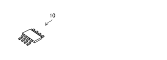
- FIG. 2 is an external perspective view of a transceiver according to an embodiment of the present disclosure.
- FIG. 3 is a configuration diagram of a transmitting circuit in a transceiver according to an embodiment of the present disclosure.
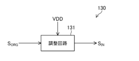
- FIG. 4 is a diagram illustrating a configuration for generating a control input signal from an original input signal according to an embodiment of the present disclosure.
- FIG. 5 is a diagram illustrating a configuration for generating an original input signal according to an embodiment of the present disclosure.
- FIG. 6 is a diagram showing the principle relationship between the original input signal and the control input signal according to the embodiment of the present disclosure.
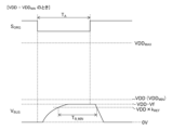
- FIG. 7 is a diagram for explaining signal output conditions according to the embodiment of the present disclosure.
- FIG. 1 is an overall configuration diagram of a communication system according to an embodiment of the present disclosure.
- FIG. 2 is an external perspective view of a transceiver according to an embodiment of the present disclosure.
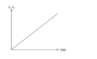
- FIG. 8 is a relationship diagram between power supply voltage and charging current or discharging current according to an embodiment of the present disclosure.
- FIG. 9 is a diagram schematically showing waveforms of a control input signal and an output voltage according to an embodiment of the present disclosure.
- FIG. 10 is a diagram schematically showing the waveforms of the control input signal and output voltage when the power supply voltage is relatively high.
- FIG. 11 is a diagram schematically showing the waveforms of the control input signal and output voltage when the power supply voltage is relatively low.
- FIG. 12 is a diagram showing how the low level width of the output voltage depends on the power supply voltage according to the reference method.
- FIG. 13 is a diagram showing how the relationship between the original input signal and the control input signal depends on the power supply voltage, according to an improved method according to an embodiment of the present disclosure.
- FIG. 14 is a diagram illustrating an example of the relationship between power supply voltage and delay time, according to an improved method according to an embodiment of the present disclosure.
- FIG. 15 is a waveform diagram of several signals and voltages according to an improved method according to an embodiment of the present disclosure.
- FIG. 16 is a diagram illustrating another example of the relationship between the power supply voltage and the delay time, according to the improved method according to the embodiment of the present disclosure.
- bus connection terminal BUS referred to by "BUS" below (see Figure 1) may be written as bus connection terminal BUS or may be abbreviated as terminal BUS, but all of them are refer to the same thing.
- Line refers to wiring through which electrical signals are propagated or applied.
- the ground refers to a reference conductive part having a reference potential of 0V (zero volts), or refers to the 0V potential itself.
- the reference conductive part may be formed using a conductor such as metal.
- the potential of 0V is sometimes referred to as a ground potential.
- voltages shown without particular reference represent potentials as seen from ground.
- Level refers to the level of potential, and for any signal or voltage of interest, a high level has a higher potential than a low level.
- a signal or voltage being at a high level strictly means that the level of the signal or voltage is at a high level, and a signal or voltage being at a low level does not strictly mean that the level of the signal or voltage is at a high level. It means that the signal or voltage level is at low level.
- a level for a signal may be expressed as a signal level, and a level for a voltage may be expressed as a voltage level.
- a switch from a low level to a high level in any signal or voltage of interest is called an up edge.
- the timing at which an up edge occurs is called an up edge timing. You can read up edge as rising edge.
- the transition from a high level to a low level in any signal or voltage of interest is called a down edge.
- the timing at which a down edge occurs is referred to as down edge timing. You can read down edge as falling edge.
- an on state refers to a state in which the drain and source of the transistor are electrically connected
- an off state refers to a state in which the drain and source of the transistor are electrically connected. Refers to the state where there is no conduction between the two (blocked state).
- the MOSFET is understood to be an enhancement type MOSFET unless otherwise specified.
- MOSFET is an abbreviation for "metal-oxide-semiconductor field-effect transistor.”
- the back gate of any MOSFET may be considered to be short-circuited to the source.
- the period during which the level of the signal is high level is referred to as the high level period
- the period during which the level of the signal is at low level is referred to as the low level period.
- Connections between multiple parts forming a circuit such as arbitrary circuit elements, wiring (lines), and nodes, may be understood to refer to electrical connections, unless otherwise specified.
- FIG. 1 shows an overall configuration diagram of a communication system 1 according to an embodiment of the present disclosure.
- the communication system 1 includes a transceiver 10, a microcomputer 20, and a counterpart device 30.
- the bus line 51, pull-up resistor 52, backflow prevention diode 53, capacitor 54, data line 61, data line 62, and pull-up resistor 63 are also included in the components of the communication system 1.
- FIG. 2 is an external perspective view of the transceiver 10.
- the transceiver 10 includes a semiconductor chip having a semiconductor integrated circuit formed on a semiconductor substrate, a housing (package) that houses the semiconductor chip, and a plurality of external terminals exposed to the outside of the transceiver 10 from the housing. It is an electronic component equipped with The transceiver 10 is formed by enclosing a semiconductor chip in a housing (package) made of resin. Note that the number of external terminals of the transceiver 10 and the type of casing of the transceiver 10 shown in FIG. 2 are merely examples, and they can be designed arbitrarily. FIG.
- a power supply terminal VIN shows a power supply terminal VIN, a bus connection terminal BUS, a ground terminal GND, a reception data output terminal RXD, and a transmission data input terminal TXD, which are included in the plurality of external terminals.
- External terminals other than these may also be provided in the transceiver 10.
- a power supply voltage VDD is supplied from a voltage source (not shown) to the power supply terminal VIN.
- Power supply voltage VDD has a predetermined positive DC voltage value.
- Transceiver 10 is driven based on power supply voltage VDD.
- a ground terminal GND is connected to ground.
- the bus connection terminal BUS is connected to one end of the bus line 51, and the other end of the bus line 51 is connected to the counterpart device 30. That is, the bus connection terminal BUS is connected to the counterpart device 30 via the bus line 51.
- the counterpart device 30 also has a terminal receiving the power supply voltage VDD and a terminal connected to the ground, and is driven based on the power supply voltage VDD.
- the bus line 51 is connected to the application end 50 of the power supply voltage VDD via a pull-up resistor 52 and a backflow prevention diode 53.
- the application terminal 50 is a terminal to which the power supply voltage VDD is applied.
- the backflow prevention diode 53 has a forward direction from the application end 50 toward the bus line 51 and the bus connection terminal BUS.
- the backflow prevention diode 53 prevents current from flowing from the bus line 51 to the application end 50 . More specifically, the anode of the backflow prevention diode 53 is connected to the application terminal 50, the cathode of the backflow prevention diode 53 is connected to one end of the pull-up resistor 52, and the other end of the pull-up resistor 52 is connected to the bus line 51. connected to.
- the application end 50 may be connected to the anode of the backflow prevention diode 53 via the pull-up resistor 52, and the cathode of the backflow prevention diode 53 may be connected to the bus line 51.
- a capacitor 54 is connected between the bus line 51 and ground. That is, one end of the capacitor 54 is connected to the bus line 51, and the other end of the capacitor 54 is connected to the ground. Note that the capacitor 54 may be composed of a plurality of capacitors separated from each other. Capacitor 54 may be omitted.
- the received data output terminal RXD is connected to one end of the data line 61, and the other end of the data line 61 is connected to the microcomputer 20.
- the transmission data input terminal TXD is connected to one end of the data line 62, and the other end of the data line 62 is connected to the microcomputer 20. That is, terminals RXD and TXD are connected to microcomputer 20 via data lines 61 and 62.
- Data line 61 is connected to the application terminal of power supply voltage VCC via pull-up resistor 63.
- Power supply voltage VCC has a predetermined positive DC voltage value. It does not matter whether the values of the power supply voltages VCC and VDD match or do not match.
- the microcomputer 20 has a terminal receiving the power supply voltage VCC and a terminal connected to the ground, and is driven based on the power supply voltage VCC.
- the transceiver 10 includes a receiving circuit RX and a transmitting circuit TX.
- the receiving circuit RX is connected to a received data output terminal RXD and a bus connection terminal BUS.
- the transmission circuit TX is connected to a transmission data input terminal TXD and a bus connection terminal BUS.
- the transceiver 10 and the other device 30 perform bidirectional communication via the bus line 51 in a half-duplex manner.
- the bidirectional communication assumed in this embodiment is serial communication using a single wire method (that is, serial communication using the bus line 51, which is one wire).
- the transceiver 10 may function as a master and the other device 30 may function as a slave, or the other device 30 may function as a master and the transceiver 10 may function as a slave.
- the two-way communication between the transceiver 10 and the other device 30 may be, for example, two-way communication based on the LIN (Local Interconnect Network) standard or the CXPI (Clock Extension Peripheral Interface) standard.
- one of the transceiver 10 and the other device 30 operates as a transmitting device, and the other functions as a receiving device.
- the transceiver 10 When the transceiver 10 functions as a receiving device, the counterpart device 30 transmits a signal (hereinafter referred to as signal S R ) via the bus line 51, and the receiving circuit RX transmits a signal to the counterpart device 30 via the bus connection terminal BUS. Receives the signal S R transmitted from the terminal. The receiving circuit RX transmits the received signal S R from the terminal RXD to the microcomputer 20 via the data line 61.
- the bus connection terminal BUS functions as an input terminal (signal receiving terminal) that receives a signal transmitted from the counterpart device 30.
- transceiver 10 When transceiver 10 functions as a transmitting device, microcomputer 20 transmits a signal (hereinafter referred to as signal S T ) to transceiver 10 via data line 62 . A signal S T from the microcomputer 20 is received at the terminal TXD.
- the transmitting circuit TX transmits the signal S T received from the microcomputer 20 to the counterpart device 30 via the bus line 51.
- the counterpart device 30 may be configured with a transceiver and microcomputer set equivalent to the transceiver 10 and the microcomputer 20, and in this case, the signal S T received from the transceiver 10 is transmitted from the transceiver in the counterpart device 30 to the counterpart device. The information is transmitted to the microcomputer in the side device 30.
- the bus connection terminal BUS functions as an output terminal (signal transmission terminal) at which a signal to be transmitted from the transceiver 10 appears.
- Transmission of a signal via the bus line 51 is realized by controlling the level of the bus line 51 to a high level or a low level.
- the level of the bus line 51 and the level of the bus connection terminal BUS are the same.
- the level of the bus line 51 is higher than 0V and lower than the power supply voltage VDD.
- VDD ⁇ k H the level of the bus line 51 corresponds to a high level
- VDD ⁇ k L the voltage (VDD ⁇ k L )
- Level 51 corresponds to the low level.
- the voltage V BUS corresponds to the output voltage (output voltage of the transmitting circuit TX). Therefore, the voltage V BUS when focusing on the configuration or operation of the transmitting circuit TX may be referred to as an output voltage hereinafter.
- the signal indicated by the output voltage V BUS can be referred to as an output signal.
- the transmission circuit TX in the transceiver 10 adjusts the slew rate of the output voltage V BUS in order to reduce radiation noise when the level of the bus line 51 changes between a high level and a low level when transmitting a signal via the bus line 51. It has the ability to control.
- FIG. 3 shows the basic configuration of the transmitting circuit TX.
- the transmission circuit TX according to the basic configuration includes an output transistor 111, a capacitor (feedback capacitor) 112, a backflow prevention diode 113, a charging/discharging circuit 120, a control input signal supply circuit 130, and a gate voltage limiting circuit 140. Be prepared.
- the output transistor 111 is an N-channel MOSFET.
- the output transistor 111 is provided between the bus connection terminal BUS functioning as an output terminal and the ground, and the transmission circuit TX transmits a signal using the output transistor 111 having an open drain configuration.
- a backflow prevention diode 113 is provided between the output transistor 111 and the bus connection terminal BUS to prevent the flow of current from the ground toward the bus line 51 via the output transistor 111 and the bus connection terminal BUS.
- the drain of the output transistor 111 is connected to the cathode of the backflow prevention diode 113, and the anode of the backflow prevention diode 113 is connected to the bus connection terminal BUS.
- the source of output transistor 111 is connected to ground.
- the gate voltage of the output transistor 111 (that is, the voltage applied to the gate of the output transistor 111) is represented by the symbol “V G ".
- the gate threshold voltage of the output transistor 111 is represented by the symbol “V G_TH “.
- the gate threshold voltage V G_TH has a positive voltage value that depends on the characteristics of the output transistor 111.
- a capacitor 112 is connected between the gate of the output transistor 111 and the bus connection terminal BUS. That is, one end of the capacitor 112 is connected to the gate of the output transistor 111, and the other end of the capacitor 112 is connected to the bus connection terminal BUS.
- the charging/discharging circuit 120 charges or discharges the gate of the output transistor 111 according to the control input signal S IN .
- the charging/discharging circuit 120 can control the output transistor 111 to turn on by charging the gate of the output transistor 111, and can control the output transistor 111 to turn off by discharging the gate of the output transistor 111.
- the control input signal S IN is a binary signal having a high or low signal level.
- the high level control input signal S IN has substantially the potential of the internal power supply voltage V REG
- the low level control input signal S IN has substantially the ground potential.
- a regulator (not shown) within transceiver 10 generates internal power supply voltage V REG , which is a positive DC voltage, from power supply voltage VDD.
- the charging/discharging circuit 120 includes a charging circuit 121 and a discharging circuit 122.
- the charging circuit 121 increases the gate voltage V G of the output transistor 111 by supplying a charging current to the gate of the output transistor 111 during the high level period of the control input signal S IN .
- the gate voltage V G has an upper limit, and the gate voltage V G does not rise beyond the upper limit voltage.
- the upper limit voltage of the gate voltage V G is the internal power supply voltage V REG or a predetermined voltage lower than the internal power supply voltage V REG .
- the upper limit voltage of the gate voltage V G is higher than the gate threshold voltage V G_TH of the output transistor 111.
- the output transistor 111 switches from the off state to the on state. Specifically, in the process of increasing the gate voltage V G from a sufficiently low voltage (for example, 0 V), when the gate voltage V G becomes equal to or higher than the gate threshold voltage V G_TH , the resistance value of the channel of the output transistor 111 sharply decreases. When the resistance value of the channel of the output transistor 111 becomes sufficiently smaller than the resistance value of the pull-up resistor 52, the voltage V BUS decreases to substantially 0V.
- the resistance value of the channel of the output transistor 111 refers to the resistance value between the drain and source of the output transistor 111.
- the discharging circuit 122 lowers the gate voltage V G of the output transistor 111 by drawing a discharge current from the gate of the output transistor 111 during the low level period of the control input signal S IN .
- the gate voltage V G has a lower limit, and the gate voltage V G does not fall below the lower limit voltage.
- the lower limit voltage of the gate voltage V G is 0V. In the process of decreasing the gate voltage V G from a voltage higher than the gate threshold voltage V G_TH , when the gate voltage V G becomes lower than the gate threshold voltage V G_TH , the output transistor 111 switches from the on state to the off state.
- the resistance value of the channel of the output transistor 111 increases sharply.
- the output voltage V BUS increases to near the power supply voltage VDD.
- the charging circuit 121 is configured by a series circuit of a charging current source 121a and a switch 121b
- the discharging circuit 122 is configured by a series circuit of a discharging current source 122a and a switch 122b.
- the charging current source 121a is provided between the application end of the internal power supply voltage V REG and the switch 121b, and generates a current I C based on the internal power supply voltage V REG .
- Switch 121b is provided between charging current source 121a and node 123.
- the discharge current source 122a is provided between the ground and the switch 122b, and generates a current I D based on the internal power supply voltage V REG .
- Switch 122b is provided between discharge current source 122a and node 123. Node 123 is connected to the gate of output transistor 111. Switches 121b and 122b are controlled to be turned on or off based on a control input signal S IN .
- a current I C (hereinafter referred to as charging current I C ) for increasing the gate voltage V G is output from the charging current source 121a via the switch 121b and the node 123. It is supplied to the gate of transistor 111.
- charging current I C a current I C for increasing the gate voltage V G is output from the charging current source 121a via the switch 121b and the node 123. It is supplied to the gate of transistor 111.
- the low level period of the control input signal S IN there is no charge exchange between the gate of the output transistor 111 and the charging circuit 121.
- the switch 121b is turned off while the switch 122b is turned on. Therefore, during the low level period of the control input signal S IN , the current I D (hereinafter referred to as discharge current I D ) for lowering the gate voltage V G is discharged from the gate of the output transistor 111 via the node 123 and the switch 122b. current source 122a.
- discharge current I D for lowering the gate voltage V G is discharged from the gate of the output transistor 111 via the node 123 and the switch 122b. current source 122a.
- the high level period of the control input signal S IN there is no charge exchange between the gate of the output transistor 111 and the discharge circuit 122.
- the control input signal supply circuit 130 generates a control input signal S IN based on the signal S T received from the microcomputer 20 and supplies the control input signal S IN to the charging/discharging circuit 120 .
- the control input signal supply circuit 130 generates the control input signal S IN through waveform shaping or the like of the signal S T .
- the configuration of the charging circuit 121 is arbitrary as long as the charging current I C can be supplied to the gate of the output transistor 111 during the high level period of the control input signal S IN .
- the charging circuit 121 may stop generating the charging current I C during the low level period of the control input signal S IN . In any case, the charging current I C flowing from the charging circuit 121 to the gate of the output transistor 111 is zero during the low level period of the control input signal S IN .
- the configuration of the discharge circuit 122 is arbitrary as long as the discharge current ID can be drawn from the gate of the output transistor 111 during the low level period of the control input signal S IN .
- the discharge circuit 122 may stop generating the discharge current ID during the high level period of the control input signal S IN . In any case, the discharge current ID flowing from the gate of the output transistor 111 to the discharge circuit 122 is zero during the high level period of the control input signal S IN .
- Gate voltage limiting circuit 140 is connected to the gate of output transistor 111 and ground.
- Gate voltage limiting circuit 140 has two diodes 141 and 142.
- the anode of diode 141 is connected to the gate of output transistor 111
- the cathode of diode 141 is connected to the anode of diode 142
- the cathode of diode 142 is connected to ground.
- the gate voltage limiting circuit 140 has a function of suppressing the gate voltage V G from exceeding a predetermined limit voltage V LIM , and may be any circuit having this function.
- the limiting voltage V LIM here is higher than the gate threshold voltage V G_TH , and corresponds to the sum of the forward voltages of the diodes 141 and 142 in the configuration example of FIG.
- the circuit 140 may be formed by a series circuit of three or more diodes.
- the output transistor 111 In the process in which the output transistor 111 is switched from the OFF state to the ON state due to an increase in the gate voltage V G based on the charging current I C , the output voltage V BUS decreases, and the decrease in the output voltage V BUS is transferred to the output transistor 111 via the capacitor 112 . feedback to the gate. Conversely, in the process in which the output transistor 111 is switched from the on state to the off state due to a decrease in the gate voltage V G based on the discharge current ID, the output voltage V BUS increases, and the increase in the output voltage V BUS is caused through the capacitor 112. It is fed back to the gate of the output transistor 111. Therefore, to the charge/discharge circuit 120, the capacitance value of the capacitor 112 appears to be equivalently larger than the actual capacitance value of the capacitor 112 due to the Miller effect. In other words, the capacitor 112 functions as a Miller capacitance.
- the control input signal supply circuit 130 includes an adjustment circuit 131 (signal generation circuit).
- the original input signal S ORG is input to the adjustment circuit 131 .
- the original input signal S ORG like the control input signal S IN , is a binary signal having a signal level of high level or low level.
- the original input signal S ORG is a signal based on the signal S T received from the microcomputer 20. Referring to FIG. 5, for example, a Schmitt trigger buffer 132 connected to the terminal TXD is provided in the control input signal supply circuit 130, and the original input signal S Generate ORG .
- the signal S T itself may be the original input signal S ORG .
- the adjustment circuit 131 generates and outputs a control input signal S IN based on the original input signal S ORG . At this time, the adjustment circuit 131 adjusts the low level width of the control input signal S IN according to the power supply voltage VDD.
- the length of the low level period and the length of the high level period of the signal or voltage of interest are referred to as a low level width and a high level width, respectively. Therefore, for example, the low level width of the control input signal S IN refers to the length of the low level period of the control input signal S IN , and the high level width of the output voltage V BUS refers to the length of the high level period of the output voltage V BUS . refers to
- the adjustment circuit 131 basically causes the control input signal S IN to have a high level during the high level period of the original input signal S ORG , and controls the control input signal S IN during the low level period of the original input signal S ORG .
- the input signal S IN also has a low level.
- the adjustment circuit 131 may change the low level width of the control input signal S IN by adjusting the low level width of the control input signal S IN based on the low level width of the control input signal S IN . It is made different from the low level width of the input signal S ORG . This will be explained in detail later.
- the slew rate of the output voltage V BUS includes a rising slew rate, which is the slew rate when the output voltage V BUS increases, and a falling slew rate, which is the slew rate when the output voltage V BUS decreases.
- the rising slew rate refers to the maximum value or average value of the rate of change of the output voltage V BUS when the output voltage V BUS rises.
- the falling slew rate refers to the maximum value or average value of the rate of change of the output voltage V BUS when the output voltage V BUS decreases.
- the rising slew rate and the falling slew rate will be collectively referred to as the output slew rate.
- the output slew rate is understood to refer to either the rising slew rate or the falling slew rate, or to both the rising slew rate and the falling slew rate.
- the output signal conditions here may be, for example, conditions defined by the LIN standard or the CXPI standard.
- FIG. 7 shows the waveforms of the original input signal S ORG and the output voltage V BUS .
- the length of the low level period of the original input signal S ORG is represented by time T A .
- the low level period and high level period of the original input signal S ORG occur alternately and repeatedly, but the length of one low level period of interest among the low level periods of the original input signal S ORG is time T A .
- the time from time t 1 to time t 3 is time T A.
- time t 2 shown in FIG. 7 is after time t 1 and before time t 3 .
- Time t 4 is a time after time t 3 .
- the output voltage V BUS continues to rise after time t 2 .
- the length between times t 2 and t 4 is expressed as time T B .
- the time T B corresponds to the high level width of the output voltage V BUS .
- the output signal condition is that the ratio of time T B to time T A , ie, the ratio (T B / TA ), is greater than or equal to a predetermined threshold value R TH .
- the forward voltage of the reverse current prevention diode 53 is represented by the symbol "Vf".
- Vf The forward voltage of the reverse current prevention diode 53.
- the power supply voltage VDD has a voltage within the power supply voltage range from the minimum voltage VDD MIN to the maximum voltage VDD MAX .
- the minimum voltage VDD MIN and the maximum voltage VDD MAX have positive predetermined voltage values satisfying "0 ⁇ VDD MIN ⁇ VDD MAX ".
- the output slew rate of the transceiver 10 is set according to the power supply voltage VDD.
- the rising slew rate depends on the charging current I C and the falling slew rate depends on the discharging current ID .
- the charging/discharging circuit 120 variably sets the respective values of the charging current I C and the discharging current ID in accordance with the power supply voltage VDD, thereby variably setting the output slew rate in accordance with the power supply voltage VDD.
- the charging circuit 121 increases the charging current I C as the power supply voltage VDD increases, and the discharging circuit 122 increases the discharging current ID as the power supply voltage VDD increases.
- the charging circuit 121 may make the charging current I C proportional to the power supply voltage VDD, and the discharging circuit 122 may make the discharging current ID proportional to the power supply voltage VDD.
- FIG. 9 shows waveform examples of the original input signal S ORG and the output voltage V BUS .
- a rectangular waveform 610 is an example of the waveform of the original input signal S ORG .
- the output slew rate is made proportional to the power supply voltage VDD by making the charging current I C and the discharging current ID proportional to the power supply voltage VDD.
- FIG. 12 shows the waveforms of the original input signal S ORG , control input signal S IN , and output voltage V BUS according to the reference method.
- the time required for the output voltage V BUS to rise by about 0.814 times the voltage (VDD - Vf) is the time required for the output voltage V BUS to rise by about 0.719 times the voltage (VDD - Vf). longer than the time it takes to As a result, in the reference method, "T B_MAX > T B_MIN ". This means that, for example, assuming that the original input signal S ORG is a periodic rectangular wave signal, the H duty of the output voltage BUS changes depending on the power supply voltage VDD.
- the output voltage BUS When the original input signal S ORG is a rectangular wave signal with periodicity, the output voltage BUS also has periodicity, and the H duty of the output voltage BUS is the high level of the output voltage BUS that occupies one cycle of the output voltage BUS . Represents the width percentage.
- the adjustment circuit 131 shown in FIG. 4 generates a down edge in the control input signal S IN in response to the down edge of the original input signal S ORG, and also generates a down edge in the control input signal S IN in response to the up edge of the original input signal S ORG . Generates an up edge on IN as well. This point does not depend on the power supply voltage VDD. However, the adjustment circuit 131 adjusts the low level width of the control input signal S IN according to the power supply voltage VDD based on the low level width of the original input signal S ORG .
- the low level width of the control input signal S IN will be different from the low level width of the original input signal S ORG .
- the adjustment circuit 131 always sets the level of the control input signal S IN to the high level (therefore, regardless of the power supply voltage VDD) during the high level period of the original input signal S ORG .
- the adjustment circuit 131 adjusts the timing from the down edge timing of the original input signal S ORG to the down edge timing of the control input signal S IN .
- a delay time T DLY is inserted depending on the power supply voltage VDD.
- the adjustment circuit 131 makes the high level period of the original input signal S ORG match the high level period of the control input signal S IN , and also makes the high level period of the original input signal S ORG coincide with the high level period of the control input signal S IN.
- the adjustment circuit 131 adjusts the level of the control input signal S IN after the delay time T DLY when the level of the original input signal S ORG transitions from high level to low level. Transition from high level to low level.
- the adjustment circuit 131 When the level of the original input signal S ORG changes from a low level to a high level, the adjustment circuit 131 immediately changes the level of the control input signal S IN from a low level to a high level without depending on the power supply voltage VDD. .
- FIG. 14 shows the relationship between the power supply voltage VDD and the delay time T DLY according to the improved method.
- the adjustment circuit 31 increases the delay time T DLY as the power supply voltage VDD increases.
- the delay time T DLY may be nonlinearly increased as the power supply voltage VDD increases.
- FIG. 15 shows the waveforms of the original input signal S ORG , control input signal S IN , and output voltage V BUS according to the improved method.
- Waveforms 660 to 662, 631', and 632' in FIG. 15 are all waveforms according to the improved method, and among these, waveform 660 is the waveform of the original input signal S ORG .
- the above difference can be made zero. can.
- an increase in the output slew rate causes an increase in radiation noise.
- the above difference can be reduced (ideally, it can be reduced to zero) without causing such an increase in radiation noise.
- the delay time T DLY is continuously changed according to the power supply voltage VDD, but the delay time T DLY may be changed stepwise according to the power supply voltage VDD.
- the delay time T DLY may be variably set in two or more stages depending on the power supply voltage VDD.
- the communication system 1 can be mounted on a vehicle such as an automobile.
- the communication system 1 can be used as a system for performing bidirectional communication in accordance with the LIN standard or the CXPI standard. More specifically, for example, communication between the transceiver 10 and the other device 30 can be used to communicate signals for realizing body control of power windows, mirrors, electric seats, door locks, etc. installed in a car. can.
- the communication system 1 is not limited to in-vehicle use.
- the communication system 1 can be applied to any application where relatively low-speed communication is performed.
- the transceiver 10 includes a signal transmitting device that generates an output signal corresponding to the original input signal S ORG at the bus connection terminal BUS functioning as an output terminal (in other words, transmits it from the bus connection terminal BUS).
- the components of the signal transmitting device include a transmitting circuit TX, and may also include a bus connection terminal BUS.
- a semiconductor device including the functions of the transceiver 10 and the microcomputer 20 may be formed, and in this case, a signal transmitting device will be provided within the semiconductor device.
- the control input signal supply circuit 130 (particularly the adjustment circuit 131) functions as a signal generation circuit that generates the control input signal S IN from the original input signal S ORG .
- the relationship between high and low levels may be reversed as described above, without detracting from the spirit of the above. Therefore, for example, a modification is made in which the high level of the original input signal S ORG is associated with the low level of the control input signal S IN , and the low level of the original input signal S ORG is associated with the high level of the control input signal S IN . Also good.
- the adjustment circuit 131 according to the modification generates a down edge in the control input signal S IN in response to an up edge of the original input signal S ORG, and generates a down edge in the control input signal S IN in response to a down edge of the original input signal S ORG . This will cause an up edge to occur.
- channels of FETs field effect transistors
- the channel type of any FET may be varied between P-channel and N-channel.
- any transistor mentioned above may be any type of transistor as long as no inconvenience occurs.
- any transistor described above as a MOSFET can be replaced with a junction FET, an IGBT (Insulated Gate Bipolar Transistor), or a bipolar transistor, as long as no inconvenience occurs.
- Any transistor has a first electrode, a second electrode, and a control electrode.
- a FET one of the first and second electrodes is the drain, the other is the source, and the control electrode is the gate.
- an IGBT one of the first and second electrodes is the collector, the other is the emitter, and the control electrode is the gate.
- a bipolar transistor that does not belong to an IGBT one of the first and second electrodes is the collector, the other is the emitter, and the control electrode is the base.
- a signal transmitting device (10) is configured to be connected to an application terminal (50) of a power supply voltage (VDD) via a pull-up resistor (52) and a reverse current prevention diode (53).
- the reverse current prevention diode has a forward direction from the power supply voltage application end toward the output terminal, and the charging/discharging circuit has a control input signal having a first level (for example, a high level).
- the output transistor when the output transistor is turned on by charging the gate of the output transistor, and when the control input signal has a second level (e.g., a low level), the output transistor is turned off by discharging the gate of the output transistor;
- the value of the charging current (I C ) and the discharging current (I D ) for the gate of the output transistor is set according to the power supply voltage, and the signal generating circuit sets the width in which the control input signal has the second level to the power supply voltage.
- This is a configuration (first configuration) that adjusts according to the voltage.
- the high level width of the output signal will vary depending on the power supply voltage even if the original input signal is constant.
- the above fluctuation can be suppressed by adjusting the width in which the control input signal has the second level according to the power supply voltage. That is, the dependence of the output signal on the power supply voltage can be reduced.
- the signal generation circuit controls the control in response to a transition of the level of the original input signal from a third level (for example, high level) to a fourth level (for example, low level).
- the level of the input signal is changed from the first level to the second level, and the level of the control input signal is changed from the second level to the second level triggered by the transition of the level of the original input signal from the fourth level to the third level.
- the signal generating circuit determines that when the power supply voltage has a predetermined first voltage value (for example, VDD MIN ) in a situation where the original input signal has a fourth level and the width is a predetermined width, A configuration (second configuration) in which the width in which the control input signal has the second level is set to be larger than when the power supply voltage has a predetermined second voltage value (for example, VDD MAX ) larger than the first voltage value. ).
- a predetermined first voltage value for example, VDD MIN
- VDD MAX predetermined second voltage value
- the signal generation circuit controls the control in response to a transition of the level of the original input signal from a third level (for example, high level) to a fourth level (for example, low level).
- the level of the input signal is changed from the first level to the second level, and the level of the control input signal is changed from the second level to the second level triggered by the transition of the level of the original input signal from the fourth level to the third level.
- the signal generation circuit sets the level of the control input signal to the first level (for example, high level) when the original input signal has a third level (for example, high level), and the signal generating circuit sets the level of the control input signal to the first level (for example, high level),
- the power source is A configuration (third configuration) may be used in which a delay time ( TDLY ) depending on the voltage can be inserted.
- the signal generation circuit is arranged such that when the power supply voltage has a predetermined first voltage value (for example, VDD MIN ), the level of the original input signal is a third level (for example, VDD MIN ).
- the level of the control input signal changes from the first level (for example, high level) to the fourth level without providing the delay time, the power supply voltage changes from the first level to the fourth level.
- the original input signal has a predetermined second voltage value (for example, VDD MAX ) larger than the voltage value, and the level of the original input signal transitions from the third level to the fourth level, the control input signal is output after the delay time. It may be a configuration (fourth configuration) in which the level of the data is transitioned from the first level to the second level.
- the charging/discharging circuit has a configuration in which the charging current and the discharging current to the gate of the output transistor are increased as the power supply voltage increases ( 5th configuration).
- the slew rate of the output signal can be increased in accordance with the increase in the power supply voltage, and as a result, the dependence of the high level width or the low level width of the output signal on the power supply voltage can be suppressed.
- the charging/discharging circuit is configured to supply the charging current to the gate of the output transistor during a period in which the control input signal has a first level. and a discharging circuit (122) configured to draw the discharge current from the gate of the output transistor during a period in which the control input signal has a second level. 6) may be used.
- the drain of the output transistor is connected to the output terminal via another backflow prevention diode (113) having a forward direction from the output terminal to the ground.
- the drain of the output transistor may be directly connected to the output terminal (seventh configuration).
Landscapes
- Engineering & Computer Science (AREA)
- Computer Hardware Design (AREA)
- Power Engineering (AREA)
- Computer Networks & Wireless Communication (AREA)
- Signal Processing (AREA)
- Physics & Mathematics (AREA)
- Computing Systems (AREA)
- General Engineering & Computer Science (AREA)
- Mathematical Physics (AREA)
- Logic Circuits (AREA)
Priority Applications (2)
| Application Number | Priority Date | Filing Date | Title |
|---|---|---|---|
| JP2024545456A JPWO2024053217A1 (https=) | 2022-09-08 | 2023-06-26 | |
| US19/073,761 US20250240017A1 (en) | 2022-09-08 | 2025-03-07 | Signal transmitting apparatus |
Applications Claiming Priority (2)
| Application Number | Priority Date | Filing Date | Title |
|---|---|---|---|
| JP2022-143092 | 2022-09-08 | ||
| JP2022143092 | 2022-09-08 |
Related Child Applications (1)
| Application Number | Title | Priority Date | Filing Date |
|---|---|---|---|
| US19/073,761 Continuation US20250240017A1 (en) | 2022-09-08 | 2025-03-07 | Signal transmitting apparatus |
Publications (1)
| Publication Number | Publication Date |
|---|---|
| WO2024053217A1 true WO2024053217A1 (ja) | 2024-03-14 |
Family
ID=90192326
Family Applications (1)
| Application Number | Title | Priority Date | Filing Date |
|---|---|---|---|
| PCT/JP2023/023589 Ceased WO2024053217A1 (ja) | 2022-09-08 | 2023-06-26 | 信号送信装置 |
Country Status (3)
| Country | Link |
|---|---|
| US (1) | US20250240017A1 (https=) |
| JP (1) | JPWO2024053217A1 (https=) |
| WO (1) | WO2024053217A1 (https=) |
Citations (4)
| Publication number | Priority date | Publication date | Assignee | Title |
|---|---|---|---|---|
| JPH1098363A (ja) * | 1996-09-19 | 1998-04-14 | Yamaha Corp | 出力バッファ回路 |
| JP2000165456A (ja) * | 1998-11-24 | 2000-06-16 | Nec Eng Ltd | ラインドライバ回路 |
| JP2011250345A (ja) * | 2010-05-31 | 2011-12-08 | Rohm Co Ltd | トランスミッタ、インタフェイス装置、車載通信システム |
| JP2017200103A (ja) * | 2016-04-28 | 2017-11-02 | ローム株式会社 | 信号処理装置及びバス通信システム |
-
2023
- 2023-06-26 WO PCT/JP2023/023589 patent/WO2024053217A1/ja not_active Ceased
- 2023-06-26 JP JP2024545456A patent/JPWO2024053217A1/ja active Pending
-
2025
- 2025-03-07 US US19/073,761 patent/US20250240017A1/en active Pending
Patent Citations (4)
| Publication number | Priority date | Publication date | Assignee | Title |
|---|---|---|---|---|
| JPH1098363A (ja) * | 1996-09-19 | 1998-04-14 | Yamaha Corp | 出力バッファ回路 |
| JP2000165456A (ja) * | 1998-11-24 | 2000-06-16 | Nec Eng Ltd | ラインドライバ回路 |
| JP2011250345A (ja) * | 2010-05-31 | 2011-12-08 | Rohm Co Ltd | トランスミッタ、インタフェイス装置、車載通信システム |
| JP2017200103A (ja) * | 2016-04-28 | 2017-11-02 | ローム株式会社 | 信号処理装置及びバス通信システム |
Also Published As
| Publication number | Publication date |
|---|---|
| JPWO2024053217A1 (https=) | 2024-03-14 |
| US20250240017A1 (en) | 2025-07-24 |
Similar Documents
| Publication | Publication Date | Title |
|---|---|---|
| US8410827B2 (en) | Transmitter, interface device, and car mounted communication system | |
| US5877647A (en) | CMOS output buffer with slew rate control | |
| US6100713A (en) | Termination circuits and methods for memory buses and devices | |
| KR101596763B1 (ko) | Can 트랜시버 회로의 제어 방법 및 장치 | |
| JP4212896B2 (ja) | 電流源を有し負荷変動に対して低感度なラインドライバ | |
| US11310072B2 (en) | Bus transceiver with ring suppression | |
| CN109714234B (zh) | 用于经由差分总线传输数据的收发器单元 | |
| US10483977B1 (en) | Level shifter | |
| CN114204926B (zh) | 半导体装置 | |
| US11387821B2 (en) | Pulse signal sending circuit | |
| US20030132794A1 (en) | Level conversion circuit | |
| JP2020025158A (ja) | 高耐圧集積回路 | |
| WO2023181633A1 (ja) | スイッチング装置及びdc/dcコンバータ | |
| WO2024053217A1 (ja) | 信号送信装置 | |
| CN113037272A (zh) | 总线驱动装置 | |
| WO2024053215A1 (ja) | 信号送信装置 | |
| US6323675B1 (en) | Termination circuits and methods therefor | |
| WO2024053216A1 (ja) | 信号送信装置 | |
| US6331786B1 (en) | Termination circuits and methods therefor | |
| WO2022185783A1 (ja) | 送信回路、電子制御ユニット、及び車両 | |
| US6323676B1 (en) | Termination circuits and methods therefor | |
| JP7680526B2 (ja) | 送信回路、電子制御ユニット、及び車両 | |
| JP2025136969A (ja) | 信号出力回路 | |
| JP2025136971A (ja) | 信号出力回路 | |
| JP3654484B2 (ja) | 出力バッファ回路 |
Legal Events
| Date | Code | Title | Description |
|---|---|---|---|
| 121 | Ep: the epo has been informed by wipo that ep was designated in this application |
Ref document number: 23862762 Country of ref document: EP Kind code of ref document: A1 |
|
| WWE | Wipo information: entry into national phase |
Ref document number: 2024545456 Country of ref document: JP |
|
| NENP | Non-entry into the national phase |
Ref country code: DE |
|
| 122 | Ep: pct application non-entry in european phase |
Ref document number: 23862762 Country of ref document: EP Kind code of ref document: A1 |