WO2024048166A1 - 照明装置 - Google Patents
照明装置 Download PDFInfo
- Publication number
- WO2024048166A1 WO2024048166A1 PCT/JP2023/028018 JP2023028018W WO2024048166A1 WO 2024048166 A1 WO2024048166 A1 WO 2024048166A1 JP 2023028018 W JP2023028018 W JP 2023028018W WO 2024048166 A1 WO2024048166 A1 WO 2024048166A1
- Authority
- WO
- WIPO (PCT)
- Prior art keywords
- light distribution
- shape
- distribution shape
- light
- value
- Prior art date
- Legal status (The legal status is an assumption and is not a legal conclusion. Google has not performed a legal analysis and makes no representation as to the accuracy of the status listed.)
- Ceased
Links
Images










Classifications
-
- F—MECHANICAL ENGINEERING; LIGHTING; HEATING; WEAPONS; BLASTING
- F21—LIGHTING
- F21V—FUNCTIONAL FEATURES OR DETAILS OF LIGHTING DEVICES OR SYSTEMS THEREOF; STRUCTURAL COMBINATIONS OF LIGHTING DEVICES WITH OTHER ARTICLES, NOT OTHERWISE PROVIDED FOR
- F21V14/00—Controlling the distribution of the light emitted by adjustment of elements
- F21V14/003—Controlling the distribution of the light emitted by adjustment of elements by interposition of elements with electrically controlled variable light transmissivity, e.g. liquid crystal elements or electrochromic devices
-
- F—MECHANICAL ENGINEERING; LIGHTING; HEATING; WEAPONS; BLASTING
- F21—LIGHTING
- F21S—NON-PORTABLE LIGHTING DEVICES; SYSTEMS THEREOF; VEHICLE LIGHTING DEVICES SPECIALLY ADAPTED FOR VEHICLE EXTERIORS
- F21S2/00—Systems of lighting devices, not provided for in main groups F21S4/00 - F21S10/00 or F21S19/00, e.g. of modular construction
-
- F—MECHANICAL ENGINEERING; LIGHTING; HEATING; WEAPONS; BLASTING
- F21—LIGHTING
- F21V—FUNCTIONAL FEATURES OR DETAILS OF LIGHTING DEVICES OR SYSTEMS THEREOF; STRUCTURAL COMBINATIONS OF LIGHTING DEVICES WITH OTHER ARTICLES, NOT OTHERWISE PROVIDED FOR
- F21V9/00—Elements for modifying spectral properties, polarisation or intensity of the light emitted, e.g. filters
- F21V9/40—Elements for modifying spectral properties, polarisation or intensity of the light emitted, e.g. filters with provision for controlling spectral properties, e.g. colour, or intensity
-
- G—PHYSICS
- G02—OPTICS
- G02F—OPTICAL DEVICES OR ARRANGEMENTS FOR THE CONTROL OF LIGHT BY MODIFICATION OF THE OPTICAL PROPERTIES OF THE MEDIA OF THE ELEMENTS INVOLVED THEREIN; NON-LINEAR OPTICS; FREQUENCY-CHANGING OF LIGHT; OPTICAL LOGIC ELEMENTS; OPTICAL ANALOGUE/DIGITAL CONVERTERS
- G02F1/00—Devices or arrangements for the control of the intensity, colour, phase, polarisation or direction of light arriving from an independent light source, e.g. switching, gating or modulating; Non-linear optics
- G02F1/01—Devices or arrangements for the control of the intensity, colour, phase, polarisation or direction of light arriving from an independent light source, e.g. switching, gating or modulating; Non-linear optics for the control of the intensity, phase, polarisation or colour
- G02F1/13—Devices or arrangements for the control of the intensity, colour, phase, polarisation or direction of light arriving from an independent light source, e.g. switching, gating or modulating; Non-linear optics for the control of the intensity, phase, polarisation or colour based on liquid crystals, e.g. single liquid crystal display cells
-
- G—PHYSICS
- G02—OPTICS
- G02F—OPTICAL DEVICES OR ARRANGEMENTS FOR THE CONTROL OF LIGHT BY MODIFICATION OF THE OPTICAL PROPERTIES OF THE MEDIA OF THE ELEMENTS INVOLVED THEREIN; NON-LINEAR OPTICS; FREQUENCY-CHANGING OF LIGHT; OPTICAL LOGIC ELEMENTS; OPTICAL ANALOGUE/DIGITAL CONVERTERS
- G02F1/00—Devices or arrangements for the control of the intensity, colour, phase, polarisation or direction of light arriving from an independent light source, e.g. switching, gating or modulating; Non-linear optics
- G02F1/01—Devices or arrangements for the control of the intensity, colour, phase, polarisation or direction of light arriving from an independent light source, e.g. switching, gating or modulating; Non-linear optics for the control of the intensity, phase, polarisation or colour
- G02F1/13—Devices or arrangements for the control of the intensity, colour, phase, polarisation or direction of light arriving from an independent light source, e.g. switching, gating or modulating; Non-linear optics for the control of the intensity, phase, polarisation or colour based on liquid crystals, e.g. single liquid crystal display cells
- G02F1/133—Constructional arrangements; Operation of liquid crystal cells; Circuit arrangements
- G02F1/1333—Constructional arrangements; Manufacturing methods
- G02F1/1347—Arrangement of liquid crystal layers or cells in which the final condition of one light beam is achieved by the addition of the effects of two or more layers or cells
-
- H—ELECTRICITY
- H05—ELECTRIC TECHNIQUES NOT OTHERWISE PROVIDED FOR
- H05B—ELECTRIC HEATING; ELECTRIC LIGHT SOURCES NOT OTHERWISE PROVIDED FOR; CIRCUIT ARRANGEMENTS FOR ELECTRIC LIGHT SOURCES, IN GENERAL
- H05B47/00—Circuit arrangements for operating light sources in general, i.e. where the type of light source is not relevant
- H05B47/10—Controlling the light source
- H05B47/105—Controlling the light source in response to determined parameters
-
- H—ELECTRICITY
- H05—ELECTRIC TECHNIQUES NOT OTHERWISE PROVIDED FOR
- H05B—ELECTRIC HEATING; ELECTRIC LIGHT SOURCES NOT OTHERWISE PROVIDED FOR; CIRCUIT ARRANGEMENTS FOR ELECTRIC LIGHT SOURCES, IN GENERAL
- H05B47/00—Circuit arrangements for operating light sources in general, i.e. where the type of light source is not relevant
- H05B47/10—Controlling the light source
- H05B47/16—Controlling the light source by timing means
-
- F—MECHANICAL ENGINEERING; LIGHTING; HEATING; WEAPONS; BLASTING
- F21—LIGHTING
- F21Y—INDEXING SCHEME ASSOCIATED WITH SUBCLASSES F21K, F21L, F21S and F21V, RELATING TO THE FORM OR THE KIND OF THE LIGHT SOURCES OR OF THE COLOUR OF THE LIGHT EMITTED
- F21Y2115/00—Light-generating elements of semiconductor light sources
- F21Y2115/10—Light-emitting diodes [LED]
-
- Y—GENERAL TAGGING OF NEW TECHNOLOGICAL DEVELOPMENTS; GENERAL TAGGING OF CROSS-SECTIONAL TECHNOLOGIES SPANNING OVER SEVERAL SECTIONS OF THE IPC; TECHNICAL SUBJECTS COVERED BY FORMER USPC CROSS-REFERENCE ART COLLECTIONS [XRACs] AND DIGESTS
- Y02—TECHNOLOGIES OR APPLICATIONS FOR MITIGATION OR ADAPTATION AGAINST CLIMATE CHANGE
- Y02B—CLIMATE CHANGE MITIGATION TECHNOLOGIES RELATED TO BUILDINGS, e.g. HOUSING, HOUSE APPLIANCES OR RELATED END-USER APPLICATIONS
- Y02B20/00—Energy efficient lighting technologies, e.g. halogen lamps or gas discharge lamps
- Y02B20/40—Control techniques providing energy savings, e.g. smart controller or presence detection
Definitions
- the present invention relates to a lighting device.
- a lighting device that combines a light source such as an LED (Light Emitting Diode) with a thin lens carved with a prism pattern, and changes the light distribution angle by changing the distance between the light source and the thin lens.
- a lighting fixture has been disclosed in which the front surface of a transparent light bulb is covered with a liquid crystal light control element and the transmittance of the liquid crystal layer is changed to switch between direct light and scattered light (for example, see Patent Document 1).
- liquid crystal light control element makes it possible to change the light distribution shape instantaneously, controlling only the instantaneous change may result in poor performance and limited applications.
- the present invention has been made in view of the above, and an object of the present invention is to provide a lighting device that can vary the shape of light distribution.
- a lighting device includes a light source section that emits light, a light distribution shape setting section that sets a light distribution shape of light from the light source section, and light distribution shape data regarding the light distribution shape. and a control section that controls the light distribution shape setting section based on the light distribution shape data, and the light distribution shape setting section controls the light distribution shape setting section based on the signal level input from the control section.
- the control section sets a light distribution shape, and when changing the signal level input to the light distribution shape setting section from a first level to a second level, the control section changes the signal level from the first level to the first level.
- the third level is set between the second level and the third level is maintained for a predetermined time, and then the third level is changed to the second level.
- FIG. 1 is a diagram showing an example of the light distribution shape of light by the lighting device of the first embodiment.
- FIG. 2 is a diagram showing a comparative example of changes in the light distribution shape of light caused by lighting devices.
- FIG. 3 is a diagram showing an example of a change in the light distribution shape of light by the lighting device of the first embodiment.
- FIG. 4 is a diagram showing an example of a change in the voltage value applied to a liquid crystal cell over time.
- FIG. 5 is a block diagram showing the functional configuration of the lighting device according to the first embodiment of the present disclosure.
- FIG. 6 is a time chart illustrating the transmission and reception of signals in each part of the lighting device of the first embodiment.
- FIG. 7 is a flowchart showing the operation of the lighting device of the first embodiment.
- FIG. 1 is a diagram showing an example of the light distribution shape of light by the lighting device of the first embodiment.
- FIG. 2 is a diagram showing a comparative example of changes in the light distribution shape of light caused by lighting devices
- FIG. 8 is a flowchart showing the operation of the lighting device of the first embodiment.
- FIG. 9 is a diagram showing an example of a screen for setting the lighting device of the first embodiment.
- FIG. 10 is a flowchart illustrating an operation when data for controlling a lighting device is saved by a terminal such as a smartphone.
- FIG. 11 is a diagram illustrating the process of changing the light distribution shape in the vertical and horizontal directions by the task control unit.
- FIG. 12 is a block diagram showing the functional configuration of a lighting device according to a second embodiment of the present disclosure.
- FIG. 13 is a flowchart showing the operation of the lighting device of the second embodiment.
- FIG. 14 is a flowchart showing the operation of the lighting device of the second embodiment.
- FIG. 15 is a diagram showing an example of a screen for setting the lighting device according to the second embodiment.
- FIG. 16 is a flowchart illustrating the operation when setting the lighting device using a terminal such as a smartphone.
- FIG. 17 is a diagram showing an example of a change in the light distribution shape over time.
- FIG. 18 is a perspective view showing an example of the optical element section according to the embodiment.
- FIG. 19 is a schematic plan view of the first substrate viewed from the Dz direction.
- FIG. 20 is a schematic plan view of the second substrate viewed from the Dz direction.
- FIG. 21 is a perspective view of a liquid crystal cell in which a first substrate and a second substrate are stacked in the Dz direction.
- FIG. 22 is a sectional view taken along the line A-A' shown in FIG.
- FIG. 23 is a diagram showing the alignment direction of the alignment film of the first substrate.
- FIG. 24 is a diagram showing the alignment direction of the alignment film of the second substrate.
- FIG. 25 is a stacked structure diagram of the optical element according to the embodiment.
- FIG. 26 is a conceptual diagram for explaining a change in the shape of light caused by the optical element according to the embodiment.
- FIG. 27 is a conceptual diagram for explaining a change in the shape of light caused by the optical element according to the embodiment.
- FIG. 28 is a conceptual diagram for explaining a change in the shape of light caused by the optical element according to the embodiment.
- FIG. 29 is a conceptual diagram for explaining a change in the shape of light caused by the optical element according to the embodiment.
- FIG. 30 is a conceptual diagram conceptually explaining light distribution control by the lighting device according to the embodiment.
- FIG. 31 is a schematic diagram showing an example of light distribution control using light distribution control areas.
- FIG. 1 is a diagram showing an example of the light distribution shape of light by the lighting device of the first embodiment.
- a lighting device 100 is provided, for example, on the ceiling of a room.
- the lighting device 100 emits light toward the floor of a room.
- the lighting device 100 has four liquid crystal cells, as described later.
- the light distribution shape Ra can be realized by the operation of the four liquid crystal cells of the lighting device 100.
- the light distribution shapes Ra and Rb are circular shapes.
- the circular light distribution shape Ra and the circular light distribution shape Rb share a center point P.
- the circular shape of the light distribution shape Ra is larger than the circular shape of the light distribution shape Rb.
- the light distribution shapes Ra and Rb can be realized by emitting light from the lighting device 100 almost directly below.
- the light distribution shape Rc and the light distribution shape Rd can be realized by the operation of the four liquid crystal cells of the lighting device 100.
- the light distribution shapes Rc and Rd are elliptical shapes.
- the ellipse of the light distribution shape Rc and the ellipse of the light distribution shape Rd share a center point P.
- the longitudinal direction of the light distribution shape Rc and the longitudinal direction of the light distribution shape Rd are orthogonal to each other.
- controlling the light distribution shape in the Dx direction may be referred to as controlling lateral diffusion.
- controlling the light distribution shape in the Dy direction may be referred to as controlling vertical diffusion.
- the magnitude of lateral diffusion can be expressed numerically as the lateral diffusion degree, and in this embodiment, the lateral diffusion degree is set in the range of 0 to 255.
- the degree of vertical diffusion is expressed as a numerical value in the range of 0 to 255.
- FIG. 2 is a diagram illustrating a comparative example of changes in the shape of light distribution caused by lighting devices.
- FIG. 2 shows an example in which the light distribution shape R1 of the light emitted from the lighting device is changed to the light distribution shape Rn.
- the degree of diffusivity in the horizontal direction (hereinafter referred to as lateral diffusivity) is assumed to be H
- the degree of diffusion in the vertical direction (hereinafter referred to as vertical diffusivity) is assumed to be V.
- the shaded area in FIG. 2 is the light distribution shape of the light.
- the horizontal direction and the vertical direction are orthogonal to each other. The same applies to subsequent explanations.
- the light distribution shape R1 shown in FIG. 2 is a vertically long shape, that is, a vertically elongated shape. Therefore, regarding the diffusivity of the light distribution shape R1, for example, the horizontal diffusivity H is "0" and the vertical diffusivity V is "170".
- the light distribution shape Rn is a horizontally long shape, that is, a horizontally long shape. Therefore, regarding the diffusivity of the light distribution shape Rn, for example, the horizontal diffusivity H is "170" and the vertical diffusivity V is "0". Therefore, the longitudinal direction of the light distribution shape R1 and the longitudinal direction of the light distribution shape Rn are orthogonal to each other.
- the vertically elongated light distribution shape R1 changes to the horizontally elongated light distribution shape Rn, as shown by the arrow Y11 in FIG.
- the light distribution shape changes to the light distribution shape Rn.
- the shape of the light distribution appears to change instantaneously.
- the application of the lighting device is not only to change the light distribution shape instantaneously, but also to change the light distribution shape from a certain light distribution shape. There may be cases where it is desired to enhance the effect by gradually or slowly changing the light distribution shape to another light distribution shape.
- FIG. 3 is a diagram showing an example of a change in the light distribution shape of light by the lighting device of the first embodiment.
- the shaded area in FIG. 3 is the light distribution shape of the light.
- the horizontal diffusivity H is "0" and the vertical diffusivity V is "170".
- the horizontal diffusivity H is "170” and the vertical diffusivity V is "0".
- light distribution shapes R2, R3, R4, etc. are inserted in the middle of the change from light distribution shape R1 to light distribution shape Rn.
- the horizontal diffusivity H is "25" and the vertical diffusivity V is "145".
- the horizontal diffusivity H is "50” and the vertical diffusivity V is "130”.
- the horizontal diffusivity H is "75” and the vertical diffusivity V is "95”.
- the light distribution shape R1 is changed to the light distribution shape R2 as shown by the arrow Y12 in FIG. 3, and then the light distribution shape R2 is changed to the light distribution shape R3 as shown by the arrow Y23. Thereafter, the light distribution shape R3 is changed to the light distribution shape R4 as shown by the arrow Y34, and then the light distribution shape R4 is changed to another light distribution shape as shown by the arrow Y45.
- the time from the time when the light distribution shape R1 changes to the light distribution shape R2 is X [ms]
- the time from the time when the light distribution shape R2 changes to the light distribution shape R3 is X [ms]
- the light distribution shape The time from R3 to the time when the light distribution shape is changed to R4 is X [ms]
- the time until the time when the light distribution shape is changed to another light distribution shape is X [ms]. That is, the light distribution shape is changed to another light distribution shape every fixed time period X [ms].
- the time interval for changing the shape of the light distribution shape (hereinafter referred to as shape change interval) is X [ms].
- the shape change interval is, for example, 100 [ms].
- the time Xtotal [ms] for changing from the light distribution shape R1 to the light distribution shape Rn is an integral multiple of X [ms].
- Xtotal [ms] is six times X [ms].
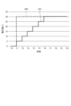
- FIG. 4 is a diagram showing an example of a change in the voltage value applied to a liquid crystal cell over time.
- the horizontal axis is time
- the vertical axis is voltage value [V].
- a broken line H40 shown in FIG. 4 shows an example of voltage change in the case of the comparative example described with reference to FIG.
- the voltage value increases from 0 [V] to 30 [V] at time T1. Thereafter, the voltage value is maintained at 30 [V] without increasing.
- this comparative example it appears to the human eye that the light distribution shape changes instantaneously.
- a solid line H41 shown in FIG. 4 shows an example of a change in voltage value in the case of the lighting device 1 according to the first embodiment of the present disclosure.
- the voltage value changes as follows. That is, at time T1, the voltage value increases from 0 [V] to 5 [V], and thereafter, the voltage value between time T1 and time T2 does not increase and is maintained at 5 [V]. Next, at time T2, the voltage value increases from 5 [V] to 10 [V], and thereafter, the voltage value between time T2 and time T3 does not increase and is maintained at 10 [V].
- the first level is changed to the third level, which is a level between the first level and the second level, and the third level is maintained for a predetermined time.
- the third level is changed to the second level.
- the voltage value is increased from 10 [V] to 15 [V]
- the voltage value between time T3 and time T4 is maintained at 15 [V] without increasing.
- the voltage value increases from 15 [V] to 20 [V]
- the voltage value between time T4 and time T5 does not increase and is maintained at 20 [V].
- the voltage value in the case of the lighting device 1 according to the first embodiment of the present disclosure increases six times in a stepwise manner as shown by the solid line H41.
- the first level is changed to the third level, which is a level between the first level and the second level, and after maintaining the third level for a predetermined time. , change from the third level to the second level. Therefore, the light distribution shape can be gradually changed, and to the human eye, it appears as if the light distribution shape has changed gradually. Therefore, it feels like the light distribution shape has changed naturally.
- the signal level that is, the voltage value input to the liquid crystal cell of the optical element section is changed multiple times, and the shape is changed multiple times.
- the amount of shape change per time is a fixed value in the first embodiment described later. That is, in the first embodiment described below, the same amount of shape change is performed multiple times. On the other hand, in a second embodiment described later, the amount of shape change at one time can be changed.
- FIG. 4 describes the case where the signal level, that is, the voltage value is increased.
- the voltage value is lowered in steps.
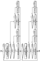
- FIG. 5 is a block diagram showing the functional configuration of the lighting device 100 according to the first embodiment of the present disclosure.
- the illumination device 100 according to the first embodiment includes a light source section 80, an optical element section 700, and a control section 60.
- the light source section 80 includes a light source 800.
- Light source 800 is, for example, an LED.
- the light source section 80 emits light in the direction of arrow Yz.
- the optical element section 700 includes a plurality of liquid crystal cells 1-1 to 1-4.
- the illumination device 100 is capable of controlling the light distribution shape of the light from the light source 800 of the light source section 80 using the optical element section 700.
- the optical element section 700 functions as a light distribution shape setting section for setting the light distribution shape of the light from the light source 800.
- the optical element section 700 includes a liquid crystal cell for p-wave polarization and a liquid crystal cell for s-wave polarization. The detailed configuration of the liquid crystal cell included in the optical element section 700 will be described later.
- the control unit 60 includes an MCU (Micro Controller Unit) 62, a D (Digital)/A (Analog) conversion unit 64, and a light source drive unit 65.
- the MCU 62 includes a storage section 61, a timer control section 621, a task control section 622, and a communication section 623.
- the MCU 62 can read various data from the storage unit 61.
- the storage unit 61 stores various data. The storage contents of the storage unit 61 will be described later.
- the MCU 62 outputs various signals to the D/A converter 64 and the light source driver 65.
- the MCU 62 controls each part of the lighting device 100.
- the timer control unit 621 manages the time and time related to the operation of the lighting device 100.
- the task control unit 622 performs calculations regarding the shape of light distribution by the lighting device 100, calculations of light distribution and dimming values, and the like.
- the communication unit 623 sends and receives signals to and from each part in the lighting device 100.
- the communication unit 623 also receives an update signal S1 transmitted from the terminal 200 such as a smartphone. As will be described later, when the settings are updated by operating the terminal 200, which is a device external to the lighting device 100, an update signal S1 is transmitted from the terminal 200, and the communication unit 623 receives this.
- the contents of the update signal S1 received by the communication unit 623 are stored in the storage unit 61.
- the D/A conversion section 64 outputs an analog signal for operating the plurality of liquid crystal cells 1-1 to 1-4 included in the optical element section 700, based on a digital signal that is a signal from the MCU 62.
- the D/A converter 64 includes a plurality of DAC (Digital-to-Analog Converter) circuits.
- the DAC circuit will be simply referred to as "DAC”.
- the D/A converter 64 includes eight DACs 64a to 64h. Each of the plurality of DACs 64a to 64h converts an input digital signal into an analog signal.
- DAC64a and DAC64b correspond to operational amplifier 67-1.
- DAC64a and DAC64b convert digital signals output from MCU62 into analog signals.
- DAC64a and DAC64b output analog signals that are input to operational amplifier 67-1.
- a digital signal may be converted into an analog signal by a plurality of DACs 64a and 64b, or a digital signal may be converted into an analog signal by one DAC.
- DAC64c and DAC64d correspond to operational amplifier 67-2.
- DAC64c and DAC64d convert the digital signal output from MCU62 into an analog signal.
- DAC64c and DAC64d output analog signals that are input to operational amplifier 67-2.
- a digital signal may be converted into an analog signal by a plurality of DACs 64c and 64d, or a digital signal may be converted into an analog signal by one DAC.
- DAC64e and DAC64f correspond to operational amplifier 67-3.
- DAC64e and DAC64f convert the digital signal output from MCU62 into an analog signal.
- DAC64e and DAC64f output analog signals that are input to operational amplifier 67-3.
- a digital signal may be converted into an analog signal by a plurality of DACs 64e and 64f, or a digital signal may be converted into an analog signal by one DAC.
- DAC64g and DAC64h correspond to operational amplifier 67-4.
- DAC64g and DAC64h convert the digital signal output from MCU62 into an analog signal.
- DAC64g and DAC64h output analog signals that are input to operational amplifier 67-4.
- a digital signal may be converted into an analog signal by a plurality of DACs 64g and 64h, or a digital signal may be converted into an analog signal by one DAC.
- the light source drive unit 65 is a controller that performs ON/OFF control of the light source 800 included in the light source unit 80 and control of the light emission intensity when ON under the control of the MCU 62.
- the controller may include one circuit or multiple circuits.
- the operational amplifiers 67-1, 67-2, 67-3, and 67-4 correspond to the liquid crystal cells 1-1, 1-2, 1-3, and 1-4.
- the operational amplifiers 67-1, 67-2, 67-3, and 67-4 input analog signals output from the D/A converter 64.
- the operational amplifiers 67-1, 67-2, 67-3, and 67-4 apply analog signals to the corresponding liquid crystal cells 1-1, 1-2, 1-3, and 1-4.
- the operational amplifiers 67-1, 67-2, 67-3, and 67-4 maintain the voltage levels of analog signals applied to the corresponding liquid crystal cells 1-1, 1-2, 1-3, and 1-4.
- the storage unit 61 of the lighting device 100 of the first embodiment includes a shape change interval holding area 611 and a diffusivity holding area 612.
- the shape change interval holding area 611 stores the value of the shape change interval.
- the diffusivity holding area 612 stores the value of the diffusivity.
- the light distribution shape of the light from the light source section 80 can be set by controlling the signal level, that is, the voltage value input to the optical element section 700.
- light distribution shapes R01, R02, R03, and R04 can be realized.
- the light distribution shape R01 is an elliptical light distribution shape.
- the light distribution shape R02 is a horizontally elongated light distribution shape.
- the light distribution shape R03 is a vertically elongated light distribution shape.
- the light distribution shape R04 is a cross-shaped light distribution shape that is a combination of a horizontally elongated light distribution shape and a vertically elongated light distribution shape.
- FIG. 6 is a time chart illustrating the transmission and reception of signals in each part of the lighting device 100 of the first embodiment.
- FIG. 6 shows the transmission and reception of signals among a terminal 200 such as a smartphone, an MCU 62, a light source 800, a D/A conversion section 64, and an optical element section 700.
- a terminal 200 such as a smartphone
- MCU 62 the transmission and reception of signals between the timer control unit 621 and the task control unit 622 is shown. Note that in FIG. 6, illustration of the operational amplifier in FIG. 5 is omitted.
- the setting content that is, the target value
- the setting content is transmitted as an update signal (S1) by operating the control application 20AP of the terminal 200.
- the task control unit 622 of the MCU 62 of the lighting device 100 receives the update signal (S1)
- the task control unit 622 outputs a timer activation signal (S2).
- the timer control unit 621 sets a timer value.
- the first timer value is, for example, 100 [ms].
- the timer control unit 621 outputs a timer out signal every time the set timer value elapses.
- the timer control unit 621 outputs a timer out signal (S3) when the set timer value elapses.
- the task control unit 622 calculates a light distribution value (S4).
- the task control unit 622 outputs a dimming signal (S5) to the light source 800.
- the dimming value and the light distribution value are controlled independently.
- the task control unit 622 outputs the dimming value set in the terminal 200 as a dimming signal. Thereafter, similarly, the dimming value set in the terminal 200 is output as a dimming signal.
- the task control unit 622 outputs a light distribution signal (S6) which is a digital signal.
- the light distribution signal (S6) is converted by the D/A converter 64 into a light distribution signal (S7) which is an analog signal.
- the light distribution signal (S7) is input to the optical element section 700, and the liquid crystal cell of the optical element section 700 performs light distribution control.
- the task control unit 622 calculates the light distribution value (S4), outputs the dimming signal (S5), outputs the light distribution signal (S6), and the D/A converter 64 calculates the light distribution signal (S7).
- S4 calculates the light distribution value
- S5 outputs the dimming signal
- S6 outputs the light distribution signal
- S7 the D/A converter 64 calculates the light distribution signal (S7).
- a series of processes for converting to The task control unit 622 performs the same process as process SS1 every time it receives a timer-out signal.
- the timer control unit 621 outputs a timer out signal (S8), and the task control unit 622 calculates the light distribution value (S9), outputs the dimming signal (S10), and controls the light distribution.
- a series of processing SS2 is performed in which the optical signal (S11) is output and the D/A converter 64 converts it into a light distribution signal (S12).
- the task control section 622 calculates the light distribution and dimming value, outputs the dimming signal, outputs the light distribution signal, and performs the D/A conversion section. A series of processing including conversion into a light distribution signal by 64 is performed.
- the voltage value changes six times. For this reason, calculation of a light distribution value (S21), output of a dimming signal (S22), output of a light distribution signal (S23), and conversion into a light distribution signal (S24) by the D/A converter 64 are performed. After processing SS6, the task control unit 622 outputs a timer stop signal (S25). As a result, the timer control unit 621 stops outputting the timer out signal.
- FIG. 7 and 8 are flowcharts showing the operation of the lighting device of the first embodiment. 7 and 8 mainly show the operation of the MCU 62.
- the transition from FIG. 7 to FIG. 8 is indicated by a circled number (1).
- the transition from FIG. 8 to FIG. 7 is indicated by a circled number (2).
- the user's operation changes the current light distribution shape in which the horizontal diffusivity H is 0 and the vertical diffusivity V is 170 to a light distribution shape in which the horizontal diffusivity H is 170 and the vertical diffusivity V is 0.
- the horizontal diffusivity and the vertical diffusivity may be collectively expressed as a diffusivity [H:0, V:170], etc.
- a case will be described in which a shape change amount is added to the current value in order to approach the horizontal target value or the vertical target value. If the target value is smaller than the current value, the amount of shape change is subtracted from the current value to approach the horizontal target value or the vertical target value.
- the terminal 200 When the user changes the degree of diffusion from the current [H: 0, V: 170] to [H: 170, V: 0] by an operation on the screen of the terminal 200, the terminal 200 The subsequent degree of diffusion (shape data) is transmitted to the lighting device 100a as an update signal S1. Specific screen operations by the user at this time will be described later. Further, the value of the degree of diffusion after the operation is a target value (horizontal target value, vertical target value).
- the task control unit 622 of the MCU 62 of the lighting device 100a receives shape data (horizontal target value (H: 170), vertical target value (V: 0)) from the terminal 200 (step S101).
- the task control unit 622 also obtains the shape change interval (X) (100 ms in this embodiment) and the shape change amount (H, V) ( ⁇ 25 in this embodiment) from the storage unit 61 (step S102). .
- the task control unit 622 starts the timer control unit 621 (step S103).
- the timer control unit 621 starts a control timer based on the shape change interval (X).
- the task control unit 622 uses a horizontal change completion flag Fh and a vertical change completion flag Fv, which indicate completion or incompleteness of processing for horizontal changes and vertical changes.
- the control timer is activated, the task control unit 622 sets the horizontal direction change completion flag Fh to "0" (incomplete) and sets the vertical direction change completion flag Fv to "0" (incomplete). do.
- step S104 the process goes into a standby state until the timer control unit 621 detects a timeout (No in step S104 ⁇ step S104).
- a timeout that is, a predetermined shape change interval (for example, 100 ms) has elapsed
- the process moves to FIG. 8 (Yes in step S104).
- the task control unit 622 determines whether the lateral direction change completion flag Fh is "0" (incomplete) (step S107).
- step S107 if the horizontal change completion flag Fh is "0" (Yes in step S107), the task control unit 622 calculates the horizontal residual ⁇ h (step S108). That is, the task control unit 622 calculates the difference between the lateral target value and the lateral current value.
- the lateral current value refers to the value of the current lateral light distribution shape, and the value changes every time the shape change interval passes.
- the task control unit 622 also determines whether the value of the horizontal residual ⁇ h calculated in step S108 is greater than 0 (step S109).
- the task control unit 622 determines that if the value of the horizontal residual ⁇ h is larger than 0, that is, if the light distribution shape is to be increased toward the horizontal target value (Yes in step S109). , it is determined whether the absolute value of the lateral residual ⁇ h is smaller than the lateral diffusivity H, which is the amount of lateral shape change (step S110). That is, it is determined whether the absolute value of the horizontal residual ⁇ h is smaller than "25", which is the horizontal diffusivity H.
- step S110 If the absolute value of the horizontal residual ⁇ h is not smaller than the horizontal diffusivity H (or higher than the horizontal diffusivity H) (No in step S110), the horizontal diffusivity is added to the current horizontal value in order to approach the horizontal target value. H is added (step S111).
- step S110 if the absolute value of the lateral residual ⁇ h is smaller than the lateral diffusivity H (Yes in step S110), it is not possible to reach the lateral target value using only the lateral diffusivity H. Therefore, the task control unit 622 adds only the lateral residual ⁇ h to the lateral current value to make the lateral current value match the lateral target value, and sets the lateral change completion flag Fh to "1" (step S115).
- step S109 if the value of the horizontal residual ⁇ h is not larger than 0 (less than or equal to 0), that is, if the light distribution shape is to be made smaller toward the horizontal target value (No in step S109), the task The control unit 622 determines whether the absolute value of the lateral residual ⁇ h is larger than the lateral diffusivity H (step S112). In step S112, if the absolute value of the horizontal residual ⁇ h is larger than H (Yes in step S112), the task control unit 622 subtracts the horizontal diffusivity H from the current horizontal value in order to approach the horizontal target value ( Step S113).
- step S112 if the absolute value of the lateral residual ⁇ h is not larger than the lateral diffusivity H (less than or equal to the lateral diffusivity H) (No in step S112), only the lateral diffusivity H is used to determine the lateral target value. I can't bring myself to do it. Therefore, the task control unit 622 subtracts only the lateral residual ⁇ h from the lateral current value so that the lateral current value matches the lateral target value, and sets the lateral change completion flag Fh to "1" (step S114).
- step S111 After step S111, S113, S114 or S115, the process moves to step S116.
- the process similarly moves to step S116.
- the task control unit 622 determines whether the vertical change completion flag Fv is "0" (incomplete) (step S116). As a result of the determination in step S116, if the vertical change completion flag Fv is "0" (Yes in step S116), the task control unit 622 calculates the vertical residual ⁇ v (step S117). ). That is, the task control unit 622 calculates the difference between the vertical target value and the vertical current value.
- the current value in the vertical direction refers to the value of the current vertical light distribution shape, and the value changes every time the shape change interval passes.
- the task control unit 622 determines whether the value of the vertical residual ⁇ v calculated in step S117 is greater than 0 (step S118). As a result of the determination in step S118, the task control unit 622 determines that if the value of the vertical residual ⁇ v is larger than 0, that is, if the light distribution shape is to be increased toward the vertical target value (Yes in step S118). , it is determined whether the absolute value of the vertical residual ⁇ v is smaller than the vertical diffusivity V, which is the amount of change in shape in the vertical direction (step S119). That is, it is determined whether the absolute value of the vertical residual ⁇ v is smaller than "25", which is the vertical diffusivity V.
- step S119 If the absolute value of the vertical residual ⁇ v is not smaller than the vertical diffusivity V in the vertical direction (it is greater than or equal to the vertical diffusivity V) (No in step S119), the current value in the vertical direction is changed in order to approach the vertical target value. Vertical diffusivity V is added (step S120).
- step S119 if the absolute value of the vertical residual ⁇ v is smaller than the vertical diffusivity V (Yes in step S119), it is possible to reach the vertical target value using only the vertical diffusivity V. Can not. Therefore, the task control unit 622 adds only the vertical residual ⁇ v to the vertical current value to make the vertical current value match the vertical target value, and sets the vertical change completion flag Fv to "1" (step S124).
- step S118 if the value of the vertical residual ⁇ v is not larger than 0 (less than or equal to 0), that is, if the light distribution shape is to be reduced toward the vertical target value (No in step S118), The task control unit 622 determines whether the absolute value of the vertical residual ⁇ v is larger than the vertical diffusivity V (step S121). In step S121, if the absolute value of the vertical residual ⁇ v is larger than the vertical diffusivity V (Yes in step S121), the task control unit 622 changes the vertical diffusivity V from the current vertical value in order to approach the vertical target value. (step S122).
- step S121 if the absolute value of the vertical residual ⁇ v is not larger than the vertical diffusivity V (less than or equal to the vertical diffusivity V) (No in step S121), only the vertical diffusivity V is used to set the vertical target value. I can't bring myself to do it. Therefore, the task control unit 622 subtracts only the vertical residual ⁇ v from the vertical current value to make the vertical current value match the vertical target value, and sets the vertical change completion flag Fv to "1" (step S123). After step S120, step S122, step S123 or S124, return to FIG. 7 and proceed to step S125. Similarly, if the vertical change completion flag Fv is "1" as a result of the determination in step S116 (No in step S116), the process returns to FIG. 7 and proceeds to step S125.
- the task control unit 622 calculates horizontal and vertical data based on the horizontal current value and the vertical current value (step S125).
- the task control unit 622 outputs digital signals corresponding to horizontal and vertical data to the D/A converter 64 (step S126).
- step S127 determines whether all controls have been completed. That is, it is determined whether the horizontal direction change completion flag Fh is "1" and the vertical direction change completion flag Fv is "1".
- step S127 if the horizontal direction change completion flag Fh is not "1" or if the vertical direction change completion flag Fv is not "1" (No in step S127), the task control unit 622 proceeds to step S104. Return and continue processing.
- step S127 if the horizontal direction change completion flag Fh is "1" and the vertical direction change completion flag Fv is "1" (Yes in step S127), the task control unit 622 controls the timer control. The operation of the control timer of the unit 621 is ended, and the series of processes is ended (step S128).
- the shape change interval and the degree of diffusion of the light distribution shape can be instructed from outside the device. For example, by installing application software in advance on a terminal such as a smartphone and activating the application software on the terminal, it is possible to instruct the shape change interval and the degree of diffusion of the light distribution shape.
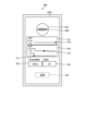
- FIG. 9 is a diagram showing an example of a screen for setting the lighting device 100 of the first embodiment.
- FIG. 9 shows an example of a screen of a terminal 200 such as a smartphone.
- FIG. 9 shows an example of a screen 200s displayed by operating the terminal 200 to start up the application software.
- the screen 200s of this example includes a light distribution possible range region 20s indicating a light distribution possible range of the lighting device 100, a light control adjustment region 21s, a light distribution adjustment region 22s, and a shape changeable region 20s.
- An interval setting area 23s and a shape change amount setting area 24s are displayed.
- the light distribution possible range area 20s is an area indicating a light distribution shape set by operating the terminal 200.
- a light distribution shape object R20 corresponding to the light distribution shape realized by the lighting device settings at that time is displayed in the light distribution possible range area 20s, and is linked to the numerical value shown in the light distribution adjustment area 22 below. are doing.
- the dimming adjustment area 21s is an area indicating a dimming adjustment value set by operating the terminal 200.
- the current set value of the dimming adjustment value is displayed in the dimming adjustment area 21s.
- the current setting value of the dimming adjustment value is "255".
- the light distribution adjustment area 22s is an area indicating a light distribution adjustment value set by operating the terminal 200.
- the light distribution adjustment area 22s displays the current light distribution shape control state on the illumination device side, that is, the current values of the degree of diffusion in the horizontal and vertical directions.
- the horizontal setting value of the light distribution adjustment value is "128".
- the set value can be changed by dragging the operating point 21h to the right or left in the figure.
- the vertical setting value of the light distribution adjustment value is "0". In the vertical direction, the setting value can be changed by dragging the operating point 21v to the right or left in the figure.
- the terminal 200 displays the diffusivity (target value) after the change in the vertical direction and the change in the horizontal direction.
- the degree of diffusion (target value) is sent to the illumination device 100 at the same time.
- a method for simultaneously sending the changed vertical diffusivity (target value) and the changed horizontal diffusivity (target value) from the terminal 200 to the lighting device 100 is as follows, for example. That is, a send button 24t may be provided on the screen 200s, and when the send button is tapped after inputting a set value, the changed diffusion degree (target value) in the vertical and horizontal directions may be sent at the same time. In addition, the transmit button 24t is not provided, the two operation points 21h and 21v are operated simultaneously with two fingers, and when the fingers are separated from the screen 200s, the degree of diffusion (target value) after changing in the vertical and horizontal directions is ) can be sent at the same time.
- the shape of the light distribution shape object R20 is changed by a swipe operation with two fingers, and when the finger moves away from the screen 200s, the degree of diffusion after changing in the vertical and horizontal directions (target value) can be sent at the same time. It is preferable that the operating points 21h and 21v move in conjunction with changes in the shape of the light distribution shape object R20.
- the shape change interval setting area 23s is an area indicating the value of the shape change interval set by operating the terminal 200.
- the current setting value of the shape change interval is displayed in the shape change interval setting area 23s.
- the current setting value of the shape change interval is "100ms”.
- the set value of the shape change interval can be changed by inputting a numerical value.
- the shape change amount setting area 24s is an area indicating the value of the shape change amount set by the operation of the terminal 200.
- the current setting value of the shape change amount is displayed in the shape change amount setting area 24s.
- the current setting value for the amount of shape change is "25". That is, the set value indicates that the amount of change in the light distribution shape in both the horizontal direction and the vertical direction is 25, and the amount of change is 25 in both the increasing direction and the decreasing direction.
- the set value of the amount of shape change can be changed by inputting a numerical value.
- the settings of the lighting device are changed, Can be sent.
- the shape change interval setting area 23s and the shape change amount setting area 24s are for changing the change amount and polarization interval time settings when changing the shape, and even if these are changed, the light distribution shape will not change. That thing doesn't change. Therefore, these numerical values can be changed at a timing different from the timing at which the light distribution shape is changed.
- changing the light distribution adjustment area 22s changes the light distribution shape itself. Therefore, the change in the light distribution shape shown in FIGS.
- the terminal 200 sends data regarding the shape change interval (X) and the amount of shape change (H, V) as the update signal (S1) based on the contents set by the operations of each area described above. It is transmitted to the lighting device 100. Therefore, the user of the lighting device 100 can use the terminal 200 to realize a desired light distribution shape with the lighting device 100.
- the storage unit 61 of the MCU 62 can store data (X) regarding the shape change interval and data (H, V) regarding the amount of shape change.
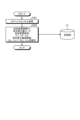
- FIG. 10 is a flowchart illustrating the operation when data for controlling the lighting device 100 is saved by a terminal such as a smartphone. As shown in FIG. 10, the lighting device 100 receives data (X) regarding the shape change interval and data (H, V) regarding the amount of shape change from the terminal 200 such as a smartphone (step S201). Next, the lighting device 100 stores the received data (X) regarding the shape change interval and the data (H, V) regarding the amount of shape change in the storage unit 61 (step S202). The lighting device 100 operates as described above based on these data stored in the storage unit 61.
- FIG. 11 is a diagram illustrating the process of changing the light distribution shape in the vertical and horizontal directions by the task control unit 622.
- the task control unit 622 approaches the vertical target value TV and the horizontal target value TH by adding the amount of shape change in each of the vertical direction (vertical direction) and the horizontal direction (horizontal direction).
- a case in which the amount of shape change is added will be described below, but by subtracting the amount of shape change, it may be possible to approach the vertical target value TV and the horizontal target value TH.
- the current value when focusing on the horizontal direction with the center point P of the light distribution shape as a reference, the current value is the horizontal current value HP1.
- the task control unit 622 adds the lateral shape change amount H1 to the lateral current value HP1.
- the current value changes to the horizontal current value HP2.
- the task control unit 622 adds the lateral shape change amount H2 to the lateral current value HP2 to obtain a new current value.
- the task control unit 622 repeats the above processing.
- the current value is the vertical current value VP1.
- the task control unit 622 adds the vertical shape change amount V1 to the vertical current value VP1.
- the current value changes to the vertical current value VP2.
- the vertical current value VP2 becomes the new current value.
- the task control unit 622 adds the vertical shape change amount V2 to the vertical current value VP2, and sets it as a new current value.
- the task control unit 622 repeats the above processing.
- FIG. 12 is a block diagram showing the functional configuration of a lighting device 100a according to a second embodiment of the present disclosure.
- the lighting device 100a according to the second embodiment differs from the lighting device 100 according to the first embodiment in the content stored in the storage unit 61.
- the illumination device 100a according to the second embodiment includes a shape change interval holding area 611 and a diffusivity holding area 612, as well as a diffusivity adjustment value holding area 613 and a shape switching time holding area 614.
- the diffusivity adjustment value holding area 613 is an area for storing the diffusivity adjustment value.
- the diffusivity adjustment value is a value for adjusting the diffusivity.
- the MCU 62 stores the spreading degree adjustment value received by the communication unit 623 from the terminal 200 in the spreading degree adjustment value holding area 613.
- the shape switching time holding area 614 is an area for storing the value of the shape switching time.
- the shape switching time indicates the time at which the shape of the light distribution shape is switched.
- the MCU 62 stores the shape switching time value received by the communication unit 623 from the terminal 200 in the shape switching time holding area 614.
- FIG. 13 and 14 are flowcharts showing the operation of the lighting device 100a of the second embodiment.
- the transition from FIG. 13 to FIG. 14 is indicated by a circled number (3).
- the transition from FIG. 14 to FIG. 13 is indicated by a circled number (4).
- 13 and 14 among the processes of the lighting device 100a of the second embodiment, what is different from the process described with reference to FIG. 7 is that the process of step S102a and the processes of step S105 and step S106 are added. That's what happened.
- the task control unit 622 of the MCU 62 receives shape data (horizontal target value, vertical target value) (step S101).
- the task control unit 622 receives from the storage unit 61 data regarding shape change time (T1, T2...Tn), shape change interval (X), shape change amount (H, V), and shape change amount adjustment.
- Data regarding the values ((H T1 , V T1 )...(H Tn , V Tn )) are acquired (step S102a).
- the task control unit 622 starts the timer control unit 621 (step S103).
- the timer control unit 621 starts a control timer based on the shape change interval (X).
- the horizontal direction change completion flag Fh is set to "0" (incomplete)
- the vertical direction change completion flag Fv is set to "0" (incomplete).
- step S104 the process goes into a standby state until the timer control unit 621 detects a timeout (No in step S104 ⁇ step S104).
- the process moves to FIG. 14 (Yes in step S104).
- the task control unit 622 determines whether there is data (T1, T2...Tn) regarding the next shape change time (step S105).
- step S105 if there is data regarding the next shape change time (Yes in step S105), the process moves to step S106, and the shape change amount is updated (step S106). That is, the horizontal shape change amount adjustment value H Tn is updated as the horizontal diffusivity H, which is the horizontal shape change amount, and the vertical shape change amount adjustment value V Tn is updated as the vertical diffusion degree, which is the vertical shape change amount. Update as degree V. After that, the process moves to step S107.
- step S105 if there is no data regarding the next shape change time (No in step S105), the process moves to step S107.
- step S107 the task control unit 622 determines whether the lateral direction change completion flag Fh is "0" (incomplete) (step S107). The subsequent processing is similar to the processing described with reference to FIGS. 7 and 8.
- FIG. 15 is a diagram showing an example of a screen for setting the lighting device 100a of the second embodiment.
- FIG. 15 shows an example of a screen of a terminal 200 such as a smartphone.
- FIG. 15 shows an example of a screen 200s displayed by operating the terminal 200 to start up the application software.
- An adjustment value setting area 26s and a shape change period setting area 27s are displayed.
- Shape change period setting area 27s "100ms", “200ms”, “300ms” and “400ms” correspond to numbers “1", “2", “3” and "4" indicating the order of shape change. Displayed.
- the first setting value is “200ms”
- the third setting value is “300ms”
- the fourth setting value is "400ms”.
- the settings of the lighting device can be changed by inputting or operating into the shape change amount adjustment value setting area 26s and the shape change period setting area 27s.
- the terminal 200 stores data regarding the shape change interval (X), shape change amount (H, V), shape change time (T1, T2...Tn), and the shape based on the contents set by the operations in each area described above. Data regarding the change amount adjustment values ((H T1 , V T1 )...(H Tn , V Tn )) is transmitted to the lighting device 100a. Therefore, the user of the lighting device 100a can use the terminal 200 to realize a desired light distribution shape with the lighting device 100a.
- FIG. 16 is a flowchart illustrating the operation when setting the lighting device 100a using a terminal such as a smartphone. As shown in FIG. 16, the lighting device 100 receives data regarding the shape change interval (X), data regarding the amount of shape change (H, V), and data regarding the shape change time (T1, T2%) from a terminal 200 such as a smartphone.
- the lighting device 100 stores these received data in the storage unit 61 (step S302).
- the lighting device 100 operates as described above based on these data stored in the storage unit 61.
- FIG. 17 is a diagram showing an example of a change in the light distribution shape over time.
- the horizontal axis represents time
- the vertical axis represents shape values.
- a change in shape in the lateral direction will be explained.
- the horizontal shape change amount adjustment value is “H T1 ”.
- This “H T1 ” is the value of the shape before change. Let the value of the changed shape be “H TX ”.
- the horizontal shape change amount adjustment value is "H T2 " at time T2. Further, at time T3, the horizontal shape change amount adjustment value is “H T3 ". Similarly, the shape changes at each time, and at time Tn, the horizontal shape change amount adjustment value is "H Tn ".
- the line connecting the shape values at each time is the solid line JH in FIG. 17.
- the shape change amount adjustment value changes in the order of “V T1 ”, “V T2 ”, “V T3 ”, ..., “V Tn ”, and the shape value after the change is “V TX ” (not shown).
- liquid crystal cell liquid crystal cell
- FIG. 18 is a perspective view showing an example of the optical element section 700 according to the embodiment.
- the Dz direction indicates the direction in which light is emitted from the light source 800 and a reflector (not shown).
- the optical element section 700 is configured by stacking a first liquid crystal cell 1-1, a second liquid crystal cell 1-2, a third liquid crystal cell 1-3, and a fourth liquid crystal cell 1-4 in the Dz direction.
- the optical element section 700 includes, from the light source 800 side (lower side of FIG. 18), a first liquid crystal cell 1-1, a second liquid crystal cell 1-2, a third liquid crystal cell 1-3, and a fourth liquid crystal cell. 1 to 4 are stacked in this order.
- FIG. 18 the light source 800 side (lower side of FIG. 18)
- the direction is the Dx direction (first direction), and the direction perpendicular to both the Dx direction and the Dz direction is the Dy direction (second direction).
- the first liquid crystal cell 1-1, the second liquid crystal cell 1-2, the third liquid crystal cell 1-3, and the fourth liquid crystal cell 1-4 each have a similar configuration.
- the first liquid crystal cell 1-1 and the fourth liquid crystal cell 1-4 are liquid crystal cells for p-wave polarization.
- the second liquid crystal cell 1-2 and the third liquid crystal cell 1-3 are liquid crystal cells for s-wave polarization.
- the first liquid crystal cell 1-1, the second liquid crystal cell 1-2, the third liquid crystal cell 1-3, and the fourth liquid crystal cell 1-4 will also be collectively referred to as "liquid crystal cell 1."
- the liquid crystal cell 1 includes a first substrate 5 and a second substrate 6.
- FIG. 19 is a schematic plan view of the first substrate viewed from the Dz direction.
- FIG. 20 is a schematic plan view of the second substrate viewed from the Dz direction. In FIG. 20, although the drive electrodes are visible through the substrate, the drive electrodes and wiring are shown in solid lines for ease of understanding.
- FIG. 21 is a perspective view of a liquid crystal cell in which a first substrate and a second substrate are stacked in the Dz direction. In FIG. 21 as well, for ease of understanding, the driving electrodes and wiring on the second substrate side are shown with solid lines, and the driving electrodes and wiring on the first substrate side are shown with dotted lines.
- FIG. 19 is a schematic plan view of the first substrate viewed from the Dz direction.
- FIG. 20 is a schematic plan view of the second substrate viewed from the Dz direction. In FIG. 20, although the drive electrodes are visible through the substrate, the drive electrodes and wiring are shown in solid lines for ease of understanding
- FIG. 22 is a sectional view taken along the line A-A' shown in FIG. 21. Note that in FIGS. 19, 20, 21, and 22, the drive electrodes 10a, 10b of the first substrate 5 extend in the Dx direction, and the drive electrodes 13a, 13b of the second substrate 6 extend in the Dy direction. A third liquid crystal cell 1-3 and a fourth liquid crystal cell 1-4 are illustrated.
- the liquid crystal cell 1 includes a liquid crystal layer 8 between a first substrate 5 and a second substrate 6, the periphery of which is sealed with a sealant 7.
- the liquid crystal layer 8 modulates the light passing through the liquid crystal layer 8 depending on the state of the electric field.
- the liquid crystal molecules positive nematic liquid crystals are used, but other liquid crystals having similar effects may also be used.
- the liquid crystal layer 8 side of the base material 9 of the first substrate 5 there are a plurality of drive electrodes 10a, 10b and a plurality of metals that supply drive voltages to be applied to these drive electrodes 10a, 10b. It includes wirings 11a and 11b, and a plurality of metal wirings 11c and 11d that supply a driving voltage to be applied to a plurality of driving electrodes 13a and 13b (see FIG. 20) provided on a second substrate 6, which will be described later.
- the metal wirings 11a, 11b, 11c, and 11d are provided in the wiring layer of the first substrate 5.
- the metal wirings 11a, 11b, 11c, and 11d are provided at intervals in the wiring layer on the first substrate 5.
- the plurality of drive electrodes 10a, 10b may be simply referred to as “drive electrodes 10.” Furthermore, the plurality of metal interconnects 11a, 11b, 11c, and 11d may be referred to as "first metal interconnects 11.” As shown in FIG. 19, in the third liquid crystal cell 1-3 and the fourth liquid crystal cell 1-4, the drive electrode 10 on the first substrate 5 extends in the Dx direction. Note that in the first liquid crystal cell 1-1 and the second liquid crystal cell 1-2, the drive electrode 10 on the first substrate 5 extends in the Dy direction.
- the plurality of drive electrodes 13a and 13b may be simply referred to as "drive electrodes 13.”
- the plurality of metal interconnects 14a and 14b may be referred to as "second metal interconnects 14.”
- the drive electrode 13 on the second substrate 6 extends in the Dy direction. Note that in the first liquid crystal cell 1-1 and the second liquid crystal cell 1-2, the drive electrode 13 on the second substrate 6 extends in the Dx direction.
- the drive electrode 10 and the drive electrode 13 are transparent electrodes formed of a transparent conductive material (transparent conductive oxide) such as ITO (Indium Tin Oxide).
- the first substrate 5 and the second substrate 6 are transparent substrates made of glass, resin, or the like.
- the first metal wiring 11 and the second metal wiring 14 are formed of at least one metal material selected from aluminum (Al), copper (Cu), silver (Ag), molybdenum (Mo), or an alloy thereof. Further, the first metal wiring 11 and the second metal wiring 14 may be a laminate in which a plurality of these metal materials are laminated. At least one metal material such as aluminum (Al), copper (Cu), silver (Ag), molybdenum (Mo), or an alloy thereof has a lower resistance than a transparent conductive oxide such as ITO.
- the metal wiring 11c of the first substrate 5 and the metal wiring 14a of the second substrate 6 are connected by a conductive portion 15a made of, for example, a conductive paste. Further, the metal wiring 11d of the first substrate 5 and the metal wiring 14b of the second substrate 6 are connected by a conductive portion 15b made of, for example, a conductive paste.
- connection terminal portion 16a that is connected to a flexible printed circuit (FPC) (not shown) is provided.
- FPC flexible printed circuit
- connection terminal portions 16a and 16b each include four connection terminals corresponding to the metal wirings 11a, 11b, 11c, and 11d.
- connection terminal portions 16a and 16b are provided on the wiring layer of the first substrate 5.
- a drive voltage is applied to the drive electrodes 10a, 10b on the first substrate 5 and the drive electrodes 13a, 13b on the second substrate 6 from the FPC connected to the connection terminal section 16a or 16b. Supplied.
- the connection terminal parts 16a and 16b may be simply referred to as "the connection terminal part 16.”
- a first substrate 5 and a second substrate 6 overlap in the Dz direction (light irradiation direction), and a plurality of drive electrodes on the first substrate 5 overlap when viewed from the Dz direction. 10 and the plurality of drive electrodes 13 on the second substrate 6 intersect.
- the liquid crystal of the liquid crystal layer 8 is controlled by supplying drive voltages to the plurality of drive electrodes 10 on the first substrate 5 and the plurality of drive electrodes 13 on the second substrate 6, respectively.
- the orientation direction of the molecules 17 can be controlled.
- the area in which the orientation direction of the liquid crystal molecules 17 in the liquid crystal layer 8 can be controlled is referred to as an "effective area AA.”
- an effective area AA By changing the refractive index distribution of the liquid crystal layer 8 in this effective area AA, it becomes possible to control the degree of diffusion of light transmitted through the effective area AA of the liquid crystal cell 1.
- the area where the liquid crystal layer 8 is sealed with the sealant 7 is referred to as a "peripheral area GA" (see FIG. 22).
- the drive electrode 10 (drive electrode 10a in FIG. 22) is covered by the alignment film 18. Further, in the effective area AA of the second substrate 6, the drive electrodes 13 (drive electrodes 13a and 13b in FIG. 22) are covered by the alignment film 19.
- the orientation film 18 and the orientation film 19 have different orientation directions of liquid crystal molecules.
- FIG. 23 is a diagram showing the orientation direction of the orientation film of the first substrate.
- FIG. 24 is a diagram showing the alignment direction of the alignment film of the second substrate.
- the alignment direction of the alignment film 18 of the first substrate 5 and the alignment direction of the alignment film 19 of the second substrate 6 are directions that intersect with each other in plan view. Specifically, as shown by the solid line arrow in FIG. 23, the alignment direction of the alignment film 18 of the first substrate 5 is perpendicular to the extending direction of the drive electrodes 10a and 10b, which is shown by the broken line arrow in FIG. Further, as shown by the solid line arrow in FIG. 24, the orientation direction of the alignment film 19 of the second substrate 6 is perpendicular to the extending direction of the drive electrodes 13a and 13b, which is shown by the broken line arrow in FIG.
- the extending direction of each of these drive electrodes 10, 13 and the alignment direction of the alignment films 18, 19 covering it are perpendicular to each other, but these may be made at an angle other than orthogonal, for example, 85° to 90°. It does not matter if they intersect within the angular range. Further, it is preferable that the drive electrodes 10 on the first substrate 5 side and the drive electrodes 13 on the second substrate 6 side are perpendicular to each other, but they may also intersect at an angle of 85° to 90°, for example. do not have.
- the alignment direction of the alignment films 18 and 19 is formed by a rubbing process or a photo alignment process.
- each liquid crystal cell 1 (first liquid crystal cell 1-1, second liquid crystal cell 1-2, third liquid crystal cell 1-3, and fourth liquid crystal cell 1-4) changes the shape of light.
- FIG. 25 is a stacked structure diagram of the optical element according to the embodiment.
- FIG. 27, FIG. 28, and FIG. 29 are conceptual diagrams for explaining changes in the shape of light caused by the optical element according to the embodiment.
- FIG. 27, FIG. 28, and FIG. 29 show examples in which a potential difference is generated between each drive electrode of the shaded substrate of each liquid crystal cell 1.
- the optical element section 700 is provided on the optical axis of the light source 800 shown by the dashed line, and as described above, from the light source 800 side (lower side in FIG. 25), the first liquid crystal cell 1- 1, a second liquid crystal cell 1-2, a third liquid crystal cell 1-3, and a fourth liquid crystal cell 1-4 are stacked in this order.
- the third liquid crystal cell 1-3 and the fourth liquid crystal cell 1-4 are stacked while being rotated by 90 degrees with respect to the first liquid crystal cell 1-1 and the second liquid crystal cell 1-2.
- each liquid crystal cell 1 as shown in FIGS. 23 and 24, the alignment directions of the alignment films intersect on the first substrate 5 side and the second substrate 6 side.
- the direction of the liquid crystal molecules in the liquid crystal layer 8 gradually changes from the Dx direction to the Dy direction (or from the Dy direction to the Dx direction) as it goes from the first substrate 5 side to the second substrate 6 side.
- the polarization component of the transmitted light rotates along the axis.
- the polarized light component that was a p-polarized light component on the first substrate 5 side changes to an s-polarized light component as it moves toward the second substrate 6 side, and the polarized light that was an s-polarized light component on the first substrate 5 side
- the component changes to a p-polarized component as it moves toward the second substrate 6 side.
- Such rotation of polarized light components may be referred to as optical rotation.
- FIG. 26 shows a state in which no potential is generated between adjacent electrodes of each liquid crystal cell 1. In this case, only optical rotation occurs in each liquid crystal cell 1, and none of the polarized light components is diffused.
- liquid crystal molecules are aligned in an arc shape between the electrodes. , thereby forming a refractive index distribution in the liquid crystal layer 8 along the Dx direction.
- the refractive index distribution acts on the polarized light component parallel to the Dx direction (the p polarized light component in FIG. 27), thereby causing the p polarized light component to be diffused in the Dx direction. do.
- the s-polarized light component is diffused in the Dy direction on the second substrate 6 side. That is, the polarized light component that changed from the p-polarized light component to the s-polarized light component while passing through the liquid crystal layer 8 of the first liquid crystal cell 1-1 is now diffused also in the Dy direction.
- the s-polarized light component when it enters the first liquid crystal cell 1-1 undergoes optical rotation while passing through the liquid crystal layer 8, but since it becomes a polarized light component that intersects with any refractive index distribution, it is not diffused but only optically rotated. and passes through the first liquid crystal cell 1-1.
- the s-polarized light component when it enters the first liquid crystal cell 1-1 changes to a p-polarized light component after passing through the first liquid crystal cell 1-1, and the p-polarized light component is transferred to the second liquid crystal cell 1-2.
- the first liquid crystal cell 1-1 acts on the p-polarized light component
- the second liquid crystal cell 1-1 acts on the s-polarized light component. 2 comes into play.
- the third liquid crystal cell 1-3 and the fourth liquid crystal cell 1-4 are rotated by 90 degrees with respect to the first liquid crystal cell 1-1 and the second liquid crystal cell 1-2
- the polarization component that acts on them Also swaps 90 degrees. That is, the third liquid crystal cell 1-3 acts on the s-polarized light component when it enters the optical element section 700, and the fourth liquid crystal cell 1-4 acts on the p-polarized light component when it enters the optical element section 700.
- the degree of light diffusion in each direction depends on the potential difference between adjacent drive electrodes 10a and 10b (or between drive electrodes 13a and 13b). If the potential difference between the drive electrodes 10a and 10b (or between the drive electrodes 13a and 13b) is a predefined maximum potential difference (for example, 30 [V]), the spread of light in that direction is the maximum (100 [%]). , if no potential difference is generated at all, no light spreads in that direction (0 [%]). Alternatively, if the potential difference between the drive electrodes 10a and 10b (or between the drive electrodes 13a and 13b) is set to 50[%] (for example, 15[V]) of the maximum potential difference, the spread of light in that direction is 50[%]. becomes. Note that if the relationship between the voltage difference and the spread of light is not linear, it is possible to set the potential difference to another potential difference instead of 15 [V].
- each liquid crystal cell 1 has a wide gap (also referred to as a cell gap) between its substrates (between the first substrate 5 and the second substrate 6), which is approximately 30 ⁇ m to 50 ⁇ m.
- the effect of the electric field formed on one substrate on the other substrate is suppressed as much as possible.
- the drive voltage that generates the potential difference between the adjacent drive electrodes 10a and 10b (or between the drive electrodes 13a and 13b) is a so-called AC square wave, and it goes without saying that this prevents burn-in of liquid crystal molecules. .
- each alignment film the extending direction of the drive electrode of each substrate, and the angle formed between these may be determined depending on the characteristics of the liquid crystal employed and the optical characteristics desired to be applied to the entire optical element section 700 or the liquid crystal cell. It can be changed appropriately for each one.
- the optical element section 700 has a structure in which four first liquid crystal cells 1-1, second liquid crystal cells 1-2, third liquid crystal cells 1-3, and fourth liquid crystal cells 1-4 are stacked.
- the structure is not limited to this, and for example, a structure in which two or three liquid crystal cells 1 are stacked, or a structure in which five or more liquid crystal cells 1 are stacked can also be adopted.
- the illumination device 1 having the above-described configuration, by controlling the driving voltage of each liquid crystal cell 1, light incident on the optical element from the light source 800 is directed in the Dx direction (horizontal diffusion direction) and the Dy direction (vertical diffusion direction). control in two directions (direction).
- the above-mentioned vertical diffusion and horizontal diffusion may be collectively referred to as light diffusion.
- the shape of the light is the shape of light appearing on a plane parallel to the output surface of the optical element, and may also be referred to as a light distribution shape. Control of light diffusivity in the present disclosure will be described below with reference to FIG. 30.
- FIG. 30 is a conceptual diagram conceptually explaining control of light diffusion degree by the lighting device according to the embodiment.
- the figure shows the irradiation range of light on the virtual plane xy perpendicular to the Dz direction. Note that the outline of the actual irradiation range becomes somewhat unclear due to the distance to the light source 800, light diffraction phenomenon, and the like.
- the liquid crystal molecules 17 of the liquid crystal layer 8 are The orientation direction is controlled. Thereby, the light distribution shape of the light emitted from the optical element section 700 is controlled.
- the light distribution shape in the Dx direction changes depending on the drive voltage applied to the drive electrode 10 or the drive electrode 13 extending in the Dy direction in each liquid crystal cell 1.
- Such diffusion of light in the Dx direction may be referred to as lateral diffusion.
- the light distribution shape in the Dy direction changes depending on the drive voltage applied to the drive electrode 10 or the drive electrode 13 extending in the Dx direction in the first to fourth liquid crystal cells.
- Such diffusion of light in the Dy direction may be referred to as vertical diffusion.
- the minimum diffusivity of horizontal diffusion and vertical diffusion is set to 0, and the maximum diffusivity is set to 255. More specifically, when the lateral diffusivity is 0, a drive electrode that functions to widen the light distribution state in the Dx direction (for example, a drive electrode that extends in the Dy direction on the first substrate 5 of the first liquid crystal cell 1-1) The electrode 10) does not affect the refractive index distribution of the liquid crystal layer 8. In this case, there is either no potential difference between the adjacent drive electrodes 10a and 10b, or no potential is supplied to the electrodes.
- the drive electrode for example, the drive electrode 10 extending in the Dy direction on the first substrate 5 of the first liquid crystal cell 1-1) that functions to widen the light distribution state in the Dx direction It has the greatest effect on the refractive index distribution of the liquid crystal layer 8.
- the potential difference between the adjacent drive electrodes 10a and 10b is set to the maximum potential difference (for example, 30 [V]) in the optical element section 700.
- the lateral diffusivity is greater than 0 and less than 255
- the potential is adjusted so that the potential difference between the adjacent drive electrodes 10a and 10b is greater than 0 [V] and smaller than the maximum potential difference (for example, 30 [V]). is applied to the electrode.
- the maximum potential difference for example, 30 [V]
- a contour a shown in FIG. 30 exemplifies the irradiation range when both the horizontal diffusivity and the vertical diffusivity are 100%. Further, a contour b shown in FIG. 30 exemplifies the irradiation range when the horizontal diffusivity is 100 [%] and the vertical diffusivity is 0 [%]. A contour c shown in FIG. 30 exemplifies the irradiation range when the horizontal diffusivity is 0 [%] and the vertical diffusivity is 100 [%]. Moreover, the contour d shown in FIG. 30 illustrates the irradiation range when both the horizontal diffusivity and the vertical diffusivity are 0%. That is, the contour d shows the light distribution state when the light from the light source 800 is emitted without being controlled in any way by the optical element section 700 (so to speak, it passes through the optical element section 700 as it is).
- the horizontal and vertical diffusivity of the light emitted from the optical element section 700 can be controlled.
- the light distribution shape of the emitted light from the lighting device 1 can be changed.
- the control for changing the light distribution shape of the light emitted from the lighting device 1 will also be referred to as "light distribution control.”
- a lighting device 1 that can control light distribution in two directions, the Dx direction and the Dy direction, is exemplified, but parameters that can be controlled in the lighting device 1 are not limited to light distribution (spread of light).
- the lighting device 1 may have a mode in which dimming control is possible.
- the controllable parameters in the lighting device 1 may include dimming (brightness).
- FIG. 31 is a schematic diagram showing an example of light distribution control using the light distribution control area LDA.
- the light distribution control area LDA is an area in which a plurality of drive electrodes 10 and a plurality of drive electrodes 13 are arranged in a plan view. That is, the light distribution control area LDA includes a plurality of electrodes extending in the Dx direction and lined up in the Dy direction, and a plurality of electrodes extending in the Dy direction and lined up in the Dx direction.
- the electrodes extending in the Dx direction and lined up in the Dy direction are, for example, the drive electrodes 10.
- the electrodes extending in the Dy direction and lined up in the Dx direction are, for example, the drive electrodes 13.
- the optical element section 700 has four liquid crystal cells 1-1 to 1-4 that overlap in the Dz direction, a plurality of electrodes extend in the Dx direction and line up in the Dy direction, and a plurality of electrodes extend in the Dy direction and line up in the Dx direction.
- the plurality of electrodes are arranged in four layers in the Dy direction.
- a plurality of electrodes extending in the Dx direction and lined up in the Dy direction and a plurality of electrodes extending in the Dy direction and lined up in the Dx direction of the four liquid crystal cells 1-1 to 1-4 included in the optical element section 700 are By controlling each potential, the light distribution control area LDA can be controlled from one side of the optical element section 700 to the other side, for example, as in examples E1, E2, E3, and E4 of "Example of light distribution shape" shown in FIG.
- the transmission range and degree of transmission of light toward the surface side can be controlled.
- Example E1 in FIG. 31 is a case where the potential difference between adjacent electrodes of a plurality of electrodes extending in the Dx direction and lined up in the Dy direction and a plurality of electrodes extending in the Dy direction and lined up in the Dx direction is all 0 volt (V).
- FIG. 2 is a schematic diagram showing a state in which the light distribution control area LDA is viewed from a plan view from the opposite side of a light source (for example, a light source 800). In example E1, the light from the light source passes through the light distribution control area LDA almost unchanged.
- FIG. 7 is a schematic diagram showing a state in which the light distribution control area LDA is viewed from a plan view from the opposite side of a light source (for example, a light source 800) when the potential difference is greater than 0 volts (V).
- a light source for example, a light source 800
- the light from the light source is distributed so that it spreads relatively largely in the Dx direction, but does not spread much in the Dy direction.
- the light distribution control area LDA is shown in a state where the light distribution control area LDA is being controlled. In this way, by making the potential difference between adjacent electrodes of the plurality of electrodes extending in the Dy direction and aligned in the Dx direction larger than the potential difference between adjacent electrodes of the plurality of electrodes extending in the Dy direction and aligned in the Dy direction. , the diffusion in the Dx direction (horizontal diffusion) can be made larger than the diffusion in the Dy direction (vertical diffusion).
- Example E3 is a potential where the potential difference between adjacent electrodes of a plurality of electrodes extending in the Dx direction and aligned in the Dy direction exceeds 0 volt (V), and between the plurality of adjacent electrodes extending in the Dy direction and aligned in the Dx direction.
- FIG. 7 is a schematic diagram showing a state in which the light distribution control area LDA is viewed from a plan view from the opposite side of the light source (for example, the light source 800) when the potential difference is 0 volt (V).
- the light from the light source spreads relatively largely in the Dy direction, but the light is distributed so that it does not spread much in the Dx direction.
- the light distribution control area LDA is shown in a state where the light distribution control area LDA is being controlled.
- the diffusion in the Dy direction vertical diffusion
- the diffusion in the Dx direction horizontal diffusion
- Example E4 is a light source when all the potentials of the plurality of electrodes extending in the Dx direction and lined up in the Dy direction and the plurality of electrodes extending in the Dy direction and lined up in the Dx direction are electric potentials exceeding 0 volts (V).
- FIG. 3 is a schematic diagram showing a state in which the light distribution control area LDA is viewed from a plan view from the opposite side of the light source 800 (for example, a light source 800).
- the light distribution control area LDA is viewed from a plan view from the opposite side of the light source 800 (for example, a light source 800).
- horizontal diffusion and vertical diffusion occur substantially simultaneously, and as a result, light distribution control is performed in a state where the entire light source is dim when viewed from the opposite side of the light source across the light distribution control area LDA. Area LDA is shown.
- the light distribution control area LDA includes, from a plan view, two or more electrodes extending in the Dx direction and lined up in the Dy direction, and two or more electrodes extending in the Dy direction and lined up in the Dx direction. All you have to do is stay there.
- one light distribution control area LDA has m electrodes extending in the Dx direction and lined up in the Dy direction, and n electrodes extending in the Dy direction and lined up in the Dx direction. This is the first condition.
- the number of electrodes for example, first electrodes 25
- the number of electrodes extending in the Dy direction is m ⁇ p.
- the second condition is that the number of electrodes (for example, second electrodes 33) arranged in the Dx direction is n ⁇ q.
- the optical element section 700 can set p light distribution control areas LDA in the Dx direction and q light distribution control areas LDA in the Dy direction in a matrix.
- m, n, p, and q are natural numbers of 2 or more.
- the entire active region (region where a liquid crystal layer is provided) of one liquid crystal cell from a plan view may be used as one light distribution control area LDA.
- examples E1, E2, E3, and E4 shown in FIG. 31 particularly show the difference in the shape of the light distribution shape in a plan view due to potential control.
- the shape of the light transmission range and the size of the light transmission range are determined by the relationship between the potential applied to the first electrode 25 and the potential applied to the second electrode 33. can be controlled more flexibly. This control allows the shape and size of the irradiated light to be changed.
Landscapes
- Physics & Mathematics (AREA)
- Chemical & Material Sciences (AREA)
- Crystallography & Structural Chemistry (AREA)
- Engineering & Computer Science (AREA)
- General Engineering & Computer Science (AREA)
- Nonlinear Science (AREA)
- Spectroscopy & Molecular Physics (AREA)
- General Physics & Mathematics (AREA)
- Optics & Photonics (AREA)
- Mathematical Physics (AREA)
- Circuit Arrangement For Electric Light Sources In General (AREA)
Abstract
Description
図1は、第1実施形態の照明装置による光の配光形状の例を示す図である。図1において、照明装置100は、例えば、部屋の天井に設けられる。照明装置100は、例えば、部屋の床に向かって光を射出する。照明装置100は、後述するように、4つの液晶セルを有している。照明装置100の4つの液晶セルの動作により、配光形状Raを実現できる。配光形状RaおよびRbは、円形形状である。配光形状Raの円形と配光形状Rbの円形とは中心点Pを共通とする。配光形状Raの円形は、配光形状Rbの円形よりも大きい。配光形状RaおよびRbは、照明装置100からほぼ真下に向かって光を照射することによって実現できる。
ここで、本開示の理解のため、光の配光形状の変化の比較例について説明する。
図3は、第1実施形態の照明装置による光の配光形状の変化の例を示す図である。図3中の網掛け部分が光の配光形状である。図3において、図2の場合と同様に、配光形状R1については、横拡散度Hが「0」、縦拡散度Vが「170」、である。配光形状Rnについては、横拡散度Hが「170」、縦拡散度Vが「0」である。比較例とは異なり、本例では、配光形状R1から、配光形状Rnまでの変化の途中に、配光形状R2、R3、R4…が挿入される。例えば、変化の途中に挿入される配光形状R2については、横拡散度Hが「25」、縦拡散度Vが「145」とする。同じく配光形状R3については、横拡散度Hが「50」、縦拡散度Vが「130」とする。同じく配光形状R4については、横拡散度Hが「75」、縦拡散度Vが「95」とする。
図5は、本開示の第1実施形態による照明装置100の機能構成を示すブロック図である。図5において、第1実施形態による照明装置100は、光源部80と、光学素子部700と、制御部60と、を有する。光源部80は、光源800を含む。光源800は、例えばLEDである。光源部80は、矢印Yzの方向に光を射出する。光学素子部700は、複数の液晶セル1-1から1-4を含む。
図6は、第1実施形態の照明装置100の各部における信号の授受を説明するタイムチャートである。図6は、スマートフォンなどの端末200、MCU62、光源800、D/A変換部64、および、光学素子部700における信号の授受を示す。MCU62については、タイマ制御部621およびタスク制御部622の信号の授受を示す。なお、図6において、図5中のオペアンプについては、図示を省略している。
照明装置100については、配光形状の形状変更間隔および拡散度を、装置の外部から指示することができる。例えば、スマートフォンなどの端末にアプリケーションソフトウェアを予めインストールしておき、端末においてアプリケーションソフトウェアを起動することによって、配光形状の形状変更間隔および拡散度を指示することができる。
図9は、第1実施形態の照明装置100の設定を行うための画面の例を示す図である。図9は、スマートフォンなどの端末200の画面の例を示す。図9は、端末200を操作してアプリケーションソフトウェアを起動することによって表示される画面200sの例を示す。図9に示すように、本例の画面200sには、照明装置100の配光可能な範囲を示す配光可能範囲領域20sと、調光調整領域21sと、配光調整領域22sと、形状変更間隔の設定領域23sと、形状変化量の設定領域24sと、が表示される。
MCU62の記憶部61には、形状変更間隔に関するデータ(X)、形状変化量に関するデータ(H、V)を保存しておくことができる。図10は、スマートフォンなどの端末によって、照明装置100を制御するためのデータを保存する場合の動作を説明するフローチャートである。図10に示すように、照明装置100は、スマートフォンなどの端末200から形状変更間隔に関するデータ(X)と、形状変化量に関するデータ(H、V)とを受信する(ステップS201)。次に、照明装置100は、受信した形状変更間隔に関するデータ(X)と、形状変化量に関するデータ(H、V)とを記憶部61に保存する(ステップS202)。照明装置100は、記憶部61に保存された、これらのデータに基づいて、上記のように動作する。
図12は、本開示の第2実施形態による照明装置100aの機能構成を示すブロック図である。図12において、第2実施形態による照明装置100aは、記憶部61に記憶する内容が第1実施形態による照明装置100とは異なる。第2実施形態による照明装置100aは、形状変更間隔保持領域611、拡散度保持領域612の他に、拡散度調整値保持領域613と、形状切替時刻保持領域614とを有する。拡散度調整値保持領域613は、拡散度調整値を記憶する領域である。拡散度調整値は、拡散度を調整するための値である。MCU62は、端末200から通信部623が受信した拡散度調整値を、拡散度調整値保持領域613に保存する。形状切替時刻保持領域614は、形状切替時刻の値を記憶する領域である。形状切替時刻は、配光形状の形状を切り替える時刻を示す。MCU62は、端末200から通信部623が受信した形状切替時刻の値を形状切替時刻保持領域614に保存する。
図15は、第2実施形態の照明装置100aの設定を行うための画面の例を示す図である。図15は、スマートフォンなどの端末200の画面の例を示す。図15は、端末200を操作してアプリケーションソフトウェアを起動することによって表示される画面200sの例を示す。第2実施形態の照明装置100aにおいては、図9を参照して説明した第1実施形態の画面200sに加えて、横方向の形状変化量調整値の設定領域25sと、縦方向の形状変化量調整値の設定領域26sと、形状変更期間の設定領域27sと、が表示される。
MCU62の記憶部61には、形状変更間隔に関するデータ(X)、形状変化量に関するデータ(H、V)、形状変更時刻に関するデータ(T1、T2…Tn)、形状変化量調整値((HT1、VT1)…(HTn、VTn))に関するデータを保存しておくことができる。図16は、スマートフォンなどの端末によって、照明装置100aを設定する場合の動作を説明するフローチャートである。図16に示すように、照明装置100は、スマートフォンなどの端末200から形状変更間隔に関するデータ(X)と、形状変化量に関するデータ(H、V)と、形状変更時刻に関するデータ(T1、T2…Tn)と、形状変化量調整値((HT1、VT1)…(HTn、VTn))に関するデータとを受信する(ステップS301)。次に、照明装置100は、受信したこれらのデータを記憶部61に保存する(ステップS302)。照明装置100は、記憶部61に保存された、これらのデータに基づいて、上記のように動作する。
図17は、時間の経過に対する、配光形状についての形状変化の例を示す図である。図17において、横軸は時間を示し、縦軸は形状の値を示す。本例では、横方向(水平方向)の形状変化に関して説明する。
次に、光学素子部700に含まれる液晶セル1-1から1-4について、図18から図30を参照して説明する。
60 制御部
61 記憶部
62 MCU
64 D/A変換部
65 光源駆動部
80 光源部
100、100a 照明装置
200 端末
621 タイマ制御部
622 タスク制御部
623 通信部
700 光学素子部
800 光源
Claims (7)
- 光を出射する光源部と、
前記光源部からの光の配光形状を設定するための配光形状設定部と、
前記配光形状に関する配光形状データを記憶する記憶部と、
前記配光形状データに基づいて前記配光形状設定部を制御する制御部と、
を含み、
前記配光形状設定部は、
前記制御部から入力される信号レベルによって前記配光形状を設定し、
前記制御部は、
前記配光形状設定部に入力する前記信号レベルを、第1レベルから第2レベルに変化させる場合に、前記第1レベルから、前記第1レベルと前記第2レベルとの間のレベルである第3レベルにし、前記第3レベルを所定時間維持した後、前記第3レベルから前記第2レベルに変化させる
照明装置。 - 前記記憶部は、
前記配光形状の形状を変更する時間間隔である形状変更間隔と、
前記配光形状の形状を変化させる量である形状変化量と、
を記憶し、
前記制御部は、
前記記憶部に記憶されている、前記形状変更間隔および前記形状変化量に基づいて、前記配光形状設定部を制御する
請求項1に記載の照明装置。 - 前記記憶部は、さらに、
前記形状変化量を調整するための値である形状変化量調整値と、
前記配光形状の形状を切り替える時刻を示す形状切替時刻と、
を記憶し、
前記制御部は、
前記記憶部に記憶されている前記形状変化量調整値に基づいて、前記形状変化量を調整し、
前記記憶部に記憶されている前記形状切替時刻に基づいて、前記配光形状の形状を変更する
請求項2に記載の照明装置。 - 前記形状変化量は、前記配光形状について、互いに直交する横方向および縦方向のそれぞれについての変化量のデータを含み、
前記制御部は、
前記横方向および前記縦方向のそれぞれについて、前記配光形状設定部を制御する
請求項2または請求項3に記載の照明装置。 - 前記制御部は、
現在の前記配光形状について、前記形状変化量を加えるまたは減じることによって新たな配光形状とし、
前記形状変化量を加えるまたは減じることを繰り返すことによって、前記配光形状を目標値の配光形状に近づける
請求項2または請求項3に記載の照明装置。 - 前記制御部は、
現在の前記配光形状と前記目標値の配光形状との差が、前記形状変化量より小さい場合、現在の前記配光形状を前記目標値の配光形状とみなす
請求項5に記載の照明装置。 - 外部の装置から送信される信号を受信する通信部をさらに含み、
前記通信部は、前記形状変化量調整値および前記形状切替時刻を受信し、
前記通信部が受信した前記形状変化量調整値および前記形状切替時刻は、前記記憶部に記憶される
請求項3に記載の照明装置。
Priority Applications (3)
| Application Number | Priority Date | Filing Date | Title |
|---|---|---|---|
| JP2024544047A JPWO2024048166A1 (ja) | 2022-09-01 | 2023-07-31 | |
| CN202380062827.2A CN119817177A (zh) | 2022-09-01 | 2023-07-31 | 照明装置 |
| US19/056,389 US12565980B2 (en) | 2022-09-01 | 2025-02-18 | Illumination device |
Applications Claiming Priority (2)
| Application Number | Priority Date | Filing Date | Title |
|---|---|---|---|
| JP2022-139366 | 2022-09-01 | ||
| JP2022139366 | 2022-09-01 |
Related Child Applications (1)
| Application Number | Title | Priority Date | Filing Date |
|---|---|---|---|
| US19/056,389 Continuation US12565980B2 (en) | 2022-09-01 | 2025-02-18 | Illumination device |
Publications (1)
| Publication Number | Publication Date |
|---|---|
| WO2024048166A1 true WO2024048166A1 (ja) | 2024-03-07 |
Family
ID=90099196
Family Applications (1)
| Application Number | Title | Priority Date | Filing Date |
|---|---|---|---|
| PCT/JP2023/028018 Ceased WO2024048166A1 (ja) | 2022-09-01 | 2023-07-31 | 照明装置 |
Country Status (4)
| Country | Link |
|---|---|
| US (1) | US12565980B2 (ja) |
| JP (1) | JPWO2024048166A1 (ja) |
| CN (1) | CN119817177A (ja) |
| WO (1) | WO2024048166A1 (ja) |
Cited By (1)
| Publication number | Priority date | Publication date | Assignee | Title |
|---|---|---|---|---|
| WO2025249065A1 (ja) * | 2024-05-31 | 2025-12-04 | 株式会社ジャパンディスプレイ | 照明装置 |
Citations (2)
| Publication number | Priority date | Publication date | Assignee | Title |
|---|---|---|---|---|
| JP2008270089A (ja) * | 2007-04-24 | 2008-11-06 | Matsushita Electric Works Ltd | 照明システム |
| WO2012074056A1 (ja) * | 2010-12-01 | 2012-06-07 | 株式会社オプトエレクトロニクス | 情報表示装置及び表示駆動方法 |
Family Cites Families (6)
| Publication number | Priority date | Publication date | Assignee | Title |
|---|---|---|---|---|
| JPH0265001A (ja) | 1988-08-30 | 1990-03-05 | Sekisui Chem Co Ltd | 照明器具の調光装置 |
| WO2023079829A1 (ja) * | 2021-11-02 | 2023-05-11 | 株式会社ジャパンディスプレイ | 照明装置 |
| WO2023105911A1 (ja) * | 2021-12-10 | 2023-06-15 | 株式会社ジャパンディスプレイ | 照明制御装置 |
| JPWO2023145347A1 (ja) * | 2022-01-26 | 2023-08-03 | ||
| JP7570541B2 (ja) * | 2022-01-27 | 2024-10-21 | 株式会社ジャパンディスプレイ | 照明装置 |
| KR102932127B1 (ko) * | 2022-08-25 | 2026-02-27 | 가부시키가이샤 재팬 디스프레이 | 조명 시스템 및 제어 장치 |
-
2023
- 2023-07-31 WO PCT/JP2023/028018 patent/WO2024048166A1/ja not_active Ceased
- 2023-07-31 CN CN202380062827.2A patent/CN119817177A/zh active Pending
- 2023-07-31 JP JP2024544047A patent/JPWO2024048166A1/ja active Pending
-
2025
- 2025-02-18 US US19/056,389 patent/US12565980B2/en active Active
Patent Citations (2)
| Publication number | Priority date | Publication date | Assignee | Title |
|---|---|---|---|---|
| JP2008270089A (ja) * | 2007-04-24 | 2008-11-06 | Matsushita Electric Works Ltd | 照明システム |
| WO2012074056A1 (ja) * | 2010-12-01 | 2012-06-07 | 株式会社オプトエレクトロニクス | 情報表示装置及び表示駆動方法 |
Cited By (1)
| Publication number | Priority date | Publication date | Assignee | Title |
|---|---|---|---|---|
| WO2025249065A1 (ja) * | 2024-05-31 | 2025-12-04 | 株式会社ジャパンディスプレイ | 照明装置 |
Also Published As
| Publication number | Publication date |
|---|---|
| US20250189102A1 (en) | 2025-06-12 |
| US12565980B2 (en) | 2026-03-03 |
| CN119817177A (zh) | 2025-04-11 |
| JPWO2024048166A1 (ja) | 2024-03-07 |
Similar Documents
| Publication | Publication Date | Title |
|---|---|---|
| JP5474775B2 (ja) | 光出力デバイス | |
| US10928580B2 (en) | Backlight module, display device and method for adjusting brightness of backlight module | |
| EP3067742B1 (en) | Liquid crystal display apparatus | |
| CN105572930A (zh) | 一种显示模组及显示系统 | |
| WO2024048166A1 (ja) | 照明装置 | |
| US11402716B2 (en) | Visual range adjustment component and driving method thereof, visual range adjustment device, and display device | |
| US20240427211A1 (en) | Optical device with light intensity sensor | |
| KR20160118433A (ko) | 표시 장치 | |
| JP2003315764A5 (ja) | ||
| CN214038022U (zh) | 一种可调光灯具 | |
| US12320478B2 (en) | Lighting device | |
| JP7746591B2 (ja) | 照明システム及び制御装置 | |
| CN110275352A (zh) | 背光模块及其透光率的调控方法 | |
| JP2009500671A (ja) | 光の形状及び方向の制御装置 | |
| WO2022143330A1 (zh) | 一种可调光灯具 | |
| CN112682727A (zh) | 一种可调光灯具 | |
| JP2016170887A (ja) | 照明装置 | |
| JP7735573B2 (ja) | 照明装置、及び照明システム | |
| WO2024135247A1 (ja) | 照明装置の制御装置 | |
| WO2024185300A1 (ja) | 照明システム | |
| US20190285963A1 (en) | Luminous display substrate, display panel and method of controlling the same, and display apparatus | |
| TW202614897A (zh) | 顯示裝置及包括其之電子裝置 | |
| JP2025157290A (ja) | 照明装置の制御装置、及び照明システム | |
| CN118732353A (zh) | 一种电致变色显示器件及其驱动方法 | |
| WO2023245424A1 (zh) | 调光玻璃切换方法 |
Legal Events
| Date | Code | Title | Description |
|---|---|---|---|
| 121 | Ep: the epo has been informed by wipo that ep was designated in this application |
Ref document number: 23859935 Country of ref document: EP Kind code of ref document: A1 |
|
| WWE | Wipo information: entry into national phase |
Ref document number: 2024544047 Country of ref document: JP |
|
| WWE | Wipo information: entry into national phase |
Ref document number: 202380062827.2 Country of ref document: CN |
|
| NENP | Non-entry into the national phase |
Ref country code: DE |
|
| WWP | Wipo information: published in national office |
Ref document number: 202380062827.2 Country of ref document: CN |
|
| 122 | Ep: pct application non-entry in european phase |
Ref document number: 23859935 Country of ref document: EP Kind code of ref document: A1 |