WO2024047973A1 - 積層セラミック電子部品の実装構造 - Google Patents
積層セラミック電子部品の実装構造 Download PDFInfo
- Publication number
- WO2024047973A1 WO2024047973A1 PCT/JP2023/019377 JP2023019377W WO2024047973A1 WO 2024047973 A1 WO2024047973 A1 WO 2024047973A1 JP 2023019377 W JP2023019377 W JP 2023019377W WO 2024047973 A1 WO2024047973 A1 WO 2024047973A1
- Authority
- WO
- WIPO (PCT)
- Prior art keywords
- electrode
- external electrode
- multilayer ceramic
- land
- ceramic electronic
- Prior art date
- Legal status (The legal status is an assumption and is not a legal conclusion. Google has not performed a legal analysis and makes no representation as to the accuracy of the status listed.)
- Ceased
Links
Images




Classifications
-
- H—ELECTRICITY
- H01—ELECTRIC ELEMENTS
- H01G—CAPACITORS; CAPACITORS, RECTIFIERS, DETECTORS, SWITCHING DEVICES, LIGHT-SENSITIVE OR TEMPERATURE-SENSITIVE DEVICES OF THE ELECTROLYTIC TYPE
- H01G2/00—Details of capacitors not covered by a single one of groups H01G4/00-H01G11/00
- H01G2/02—Mountings
- H01G2/06—Mountings specially adapted for mounting on a printed-circuit support
-
- H—ELECTRICITY
- H01—ELECTRIC ELEMENTS
- H01G—CAPACITORS; CAPACITORS, RECTIFIERS, DETECTORS, SWITCHING DEVICES, LIGHT-SENSITIVE OR TEMPERATURE-SENSITIVE DEVICES OF THE ELECTROLYTIC TYPE
- H01G4/00—Fixed capacitors; Processes of their manufacture
- H01G4/002—Details
- H01G4/018—Dielectrics
- H01G4/06—Solid dielectrics
- H01G4/08—Inorganic dielectrics
- H01G4/12—Ceramic dielectrics
-
- H—ELECTRICITY
- H01—ELECTRIC ELEMENTS
- H01G—CAPACITORS; CAPACITORS, RECTIFIERS, DETECTORS, SWITCHING DEVICES, LIGHT-SENSITIVE OR TEMPERATURE-SENSITIVE DEVICES OF THE ELECTROLYTIC TYPE
- H01G4/00—Fixed capacitors; Processes of their manufacture
- H01G4/002—Details
- H01G4/228—Terminals
- H01G4/232—Terminals electrically connecting two or more layers of a stacked or rolled capacitor
-
- H—ELECTRICITY
- H01—ELECTRIC ELEMENTS
- H01G—CAPACITORS; CAPACITORS, RECTIFIERS, DETECTORS, SWITCHING DEVICES, LIGHT-SENSITIVE OR TEMPERATURE-SENSITIVE DEVICES OF THE ELECTROLYTIC TYPE
- H01G4/00—Fixed capacitors; Processes of their manufacture
- H01G4/002—Details
- H01G4/228—Terminals
- H01G4/232—Terminals electrically connecting two or more layers of a stacked or rolled capacitor
- H01G4/2325—Terminals electrically connecting two or more layers of a stacked or rolled capacitor characterised by the material of the terminals
-
- H—ELECTRICITY
- H01—ELECTRIC ELEMENTS
- H01G—CAPACITORS; CAPACITORS, RECTIFIERS, DETECTORS, SWITCHING DEVICES, LIGHT-SENSITIVE OR TEMPERATURE-SENSITIVE DEVICES OF THE ELECTROLYTIC TYPE
- H01G4/00—Fixed capacitors; Processes of their manufacture
- H01G4/30—Stacked capacitors
-
- H—ELECTRICITY
- H05—ELECTRIC TECHNIQUES NOT OTHERWISE PROVIDED FOR
- H05K—PRINTED CIRCUITS; CASINGS OR CONSTRUCTIONAL DETAILS OF ELECTRIC APPARATUS; MANUFACTURE OF ASSEMBLAGES OF ELECTRICAL COMPONENTS
- H05K1/00—Printed circuits
- H05K1/02—Details
- H05K1/11—Printed elements for providing electric connections to or between printed circuits
- H05K1/111—Pads for surface mounting, e.g. lay-out
-
- H—ELECTRICITY
- H05—ELECTRIC TECHNIQUES NOT OTHERWISE PROVIDED FOR
- H05K—PRINTED CIRCUITS; CASINGS OR CONSTRUCTIONAL DETAILS OF ELECTRIC APPARATUS; MANUFACTURE OF ASSEMBLAGES OF ELECTRICAL COMPONENTS
- H05K1/00—Printed circuits
- H05K1/18—Printed circuits structurally associated with non-printed electric components
- H05K1/181—Printed circuits structurally associated with non-printed electric components associated with surface mounted components
-
- H—ELECTRICITY
- H05—ELECTRIC TECHNIQUES NOT OTHERWISE PROVIDED FOR
- H05K—PRINTED CIRCUITS; CASINGS OR CONSTRUCTIONAL DETAILS OF ELECTRIC APPARATUS; MANUFACTURE OF ASSEMBLAGES OF ELECTRICAL COMPONENTS
- H05K3/00—Apparatus or processes for manufacturing printed circuits
- H05K3/30—Assembling printed circuits with electric components, e.g. with resistors
- H05K3/32—Assembling printed circuits with electric components, e.g. with resistors electrically connecting electric components or wires to printed circuits
- H05K3/34—Assembling printed circuits with electric components, e.g. with resistors electrically connecting electric components or wires to printed circuits by soldering
- H05K3/341—Surface mounted components
- H05K3/3431—Leadless components
- H05K3/3442—Leadless components having edge contacts, e.g. leadless chip capacitors, chip carriers
-
- H—ELECTRICITY
- H05—ELECTRIC TECHNIQUES NOT OTHERWISE PROVIDED FOR
- H05K—PRINTED CIRCUITS; CASINGS OR CONSTRUCTIONAL DETAILS OF ELECTRIC APPARATUS; MANUFACTURE OF ASSEMBLAGES OF ELECTRICAL COMPONENTS
- H05K2201/00—Indexing scheme relating to printed circuits covered by H05K1/00
- H05K2201/10—Details of components or other objects attached to or integrated in a printed circuit board
- H05K2201/10007—Types of components
- H05K2201/10015—Non-printed capacitor
-
- H—ELECTRICITY
- H05—ELECTRIC TECHNIQUES NOT OTHERWISE PROVIDED FOR
- H05K—PRINTED CIRCUITS; CASINGS OR CONSTRUCTIONAL DETAILS OF ELECTRIC APPARATUS; MANUFACTURE OF ASSEMBLAGES OF ELECTRICAL COMPONENTS
- H05K2201/00—Indexing scheme relating to printed circuits covered by H05K1/00
- H05K2201/10—Details of components or other objects attached to or integrated in a printed circuit board
- H05K2201/10007—Types of components
- H05K2201/10022—Non-printed resistor
-
- H—ELECTRICITY
- H05—ELECTRIC TECHNIQUES NOT OTHERWISE PROVIDED FOR
- H05K—PRINTED CIRCUITS; CASINGS OR CONSTRUCTIONAL DETAILS OF ELECTRIC APPARATUS; MANUFACTURE OF ASSEMBLAGES OF ELECTRICAL COMPONENTS
- H05K2201/00—Indexing scheme relating to printed circuits covered by H05K1/00
- H05K2201/10—Details of components or other objects attached to or integrated in a printed circuit board
- H05K2201/10007—Types of components
- H05K2201/1003—Non-printed inductor
Definitions
- the present invention relates to a mounting structure for laminated ceramic electronic components.
- Patent Document 1 discloses a multilayer ceramic capacitor as such a multilayer ceramic electronic component.
- Such a multilayer ceramic capacitor consists of a laminate in which multiple dielectric layers made of ceramic materials and multiple internal electrode layers (internal conductor layers) are laminated, and two layers arranged on two end faces of the laminate, respectively. and an external electrode.
- the external electrode of the multilayer ceramic electronic component is connected to the land electrode of the circuit board.
- fillets of paste solder are formed on the external electrodes on the end faces of the multilayer ceramic electronic component in the mounting process of the multilayer ceramic electronic component, thereby stabilizing the mounting posture of the multilayer ceramic electronic component.
- fillets of paste solder are formed on the end surfaces of multilayer ceramic electronic components in the mounting process of multilayer ceramic electronic components in which external electrodes are not arranged on the end surfaces. Because the mounting position of the laminated ceramic electronic component is not stable, for example, it may float or tilt. Such a decrease in the stability of the mounting posture has sometimes occurred more significantly as multilayer ceramic electronic components have become smaller.
- An object of the present invention is to provide a mounting structure for laminated ceramic electronic components that suppresses deterioration in stability of mounting posture.
- the multilayer ceramic electronic component mounting structure is a multilayer ceramic electronic component mounting structure in which the multilayer ceramic electronic component is mounted on a circuit board.
- the multilayer ceramic electronic component is a multilayer body in which a plurality of dielectric layers and internal conductor layers made of ceramic materials are stacked, and has two main surfaces facing each other in the thickness direction and a main surface intersecting in the thickness direction.
- the laminate has two side faces facing each other in the width direction and two end faces facing each other in the length direction intersecting the thickness direction and the width direction, and only the two main faces of the laminate, Alternatively, only one of the two main surfaces of the laminate is provided with a first external electrode and a second external electrode that are spaced apart in the length direction.
- the circuit board has a first land electrode and a second land electrode that are spaced apart in the length direction and are connected to the first external electrode and the second external electrode of the multilayer ceramic electronic component, respectively. Equipped with a land electrode.
- the inner end of the first external electrode on the second external electrode side in the length direction is smaller than the inner end of the first land electrode on the second land electrode side in the length direction. It is located on the second external electrode side and the second land electrode side, and the inner end of the second external electrode on the first external electrode side in the length direction is located on the second land electrode side. is located closer to the first external electrode and the first land electrode than the inner end on the first land electrode side in the length direction.
- the present invention in the mounting structure of a multilayer ceramic electronic component, it is possible to suppress a decrease in the stability of the mounting posture.
- FIG. 1 is a perspective view showing a multilayer ceramic capacitor (multilayer ceramic electronic component) according to the present embodiment.
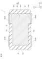
- 2 is a cross-sectional view (WT cross-section) taken along line II-II of the multilayer ceramic capacitor (multilayer ceramic electronic component) shown in FIG. 1.
- FIG. 3 is a cross-sectional view (LT cross-section) taken along the line IIIA-IIIA of the multilayer ceramic capacitor (multilayer ceramic electronic component) shown in FIG. 2.
- FIG. 3 is a cross-sectional view (LT cross-section) taken along the line IIIB-IIIB of the multilayer ceramic capacitor (multilayer ceramic electronic component) shown in FIG. 2.
- FIG. FIG. 1 is a perspective view showing a mounting structure of a multilayer ceramic capacitor (multilayer ceramic electronic component) according to the present embodiment.
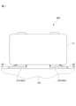
- FIG. 1 is a side view showing a mounting structure of a multilayer ceramic capacitor (multilayer ceramic electronic component) according to the present embodiment.
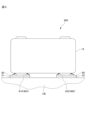
- FIG. 1 is a side view showing a mounting structure of a multilayer ceramic capacitor (multilayer ceramic electronic component) according to the present embodiment.
- FIG. 3 is a side view showing a mounting structure of a multilayer ceramic capacitor (multilayer ceramic electronic component) according to a comparative example.
- FIG. 3 is a side view showing a mounting structure of a multilayer ceramic capacitor (multilayer ceramic electronic component) according to a comparative example.
- FIG. 1 is a perspective view showing a multilayer ceramic capacitor (multilayer ceramic electronic component) according to the present embodiment
- FIG. 2 is a sectional view taken along line II-II of the multilayer ceramic capacitor (multilayer ceramic electronic component) shown in FIG. WT cross section).
- 3A is a cross-sectional view (LT cross-section) taken along line IIIA-IIIA of the multilayer ceramic capacitor (multilayer ceramic electronic component) shown in FIG. -IIIB line cross-sectional view (LT cross-section).
- a multilayer ceramic capacitor (multilayer ceramic electronic component) 1 shown in FIGS. 1 to 3B includes a multilayer body 10 and two sets of external electrodes 40. Each of the external electrodes 40 includes a first external electrode 41 and a second external electrode 42 .
- FIGS. 1 to 3B An XYZ orthogonal coordinate system is shown in FIGS. 1 to 3B and the drawings described below.
- the X direction is the length direction L of the multilayer ceramic capacitor 1 and the laminate 10
- the Y direction is the width direction W of the multilayer ceramic capacitor 1 and the laminate 10
- the Z direction is the thickness direction of the multilayer ceramic capacitor 1 and the laminate 10.
- the horizontal direction is T. Accordingly, the cross section shown in FIG. 2 is also referred to as a WT cross section, and the cross sections shown in FIGS. 3A and 3B are also referred to as an LT cross section.
- length direction L, width direction W, and thickness direction T are not necessarily orthogonal to each other, but may be intersecting with each other.
- the laminate 10 has a substantially rectangular parallelepiped shape, and has a first main surface TS1 and a second main surface TS2 facing each other in the thickness direction T, and a first side surface WS1 and a second side surface WS2 facing each other in the width direction W. and a first end surface LS1 and a second end surface LS2 facing each other in the length direction L.
- a corner is a part where three sides of the laminate 10 intersect, and a ridgeline is a part where two sides of the laminate 10 intersect.
- the laminate 10 includes a plurality of dielectric layers 20 and a plurality of internal electrode layers 30 stacked in the width direction W. Further, the laminate 10 includes, in the width direction W, that is, in the lamination direction, an inner layer portion 100, and a first outer layer portion 101 and a second outer layer portion 102 that are arranged to sandwich the inner layer portion 100.
- the inner layer section 100 includes a portion of a plurality of dielectric layers 20 and a plurality of internal electrode layers (internal conductor layers) 30. In the inner layer section 100, a plurality of internal electrode layers 30 are arranged facing each other with the dielectric layer 20 in between.
- the inner layer portion 100 is a portion (effective region) that generates capacitance and essentially functions as a capacitor.
- the first outer layer section 101 is arranged on the first side surface WS1 side of the stacked body 10, and the second outer layer section 102 is arranged on the second side surface WS2 side of the stacked body 10. More specifically, the first outer layer portion 101 is disposed between the internal electrode layer 30 closest to the first side surface WS1 among the plurality of internal electrode layers 30 and the first side surface WS1, and The outer layer portion 102 of No. 2 is disposed between the inner electrode layer 30 closest to the second side surface WS2 among the plurality of inner electrode layers 30 and the second side surface WS2.
- the first outer layer section 101 and the second outer layer section 102 do not include the internal electrode layer 30 and each include a portion of the plurality of dielectric layers 20 other than a portion for the inner layer section 100.
- the first outer layer section 101 and the second outer layer section 102 are portions that function as a protective layer of the inner layer section 100.
- dielectric layer 20 As a material for the dielectric layer 20, for example, a dielectric ceramic containing BaTiO 3 , CaTiO 3 , SrTiO 3 , CaZrO 3 or the like as a main component can be used. Further, as the material of the dielectric layer 20, a Mn compound, an Fe compound, a Cr compound, a Co compound, a Ni compound, or the like may be added as a subcomponent. More specifically, dielectric layer 20 includes a plurality of dielectric grains. The dielectric grain is a barium titanate ceramic such as a perovskite compound containing Ba and Ti. The dielectric grains may contain at least one of La, Ce, Pr, Nd, Sm, Eu, Gd, Tb, Dy, Ho, Er, Tm, Yb, Lu, and Y as a subcomponent.
- the thickness of the dielectric layer 20 is not particularly limited, but may be, for example, 0.40 ⁇ m or more and 1.0 ⁇ m or less.
- the number of dielectric layers 20 is not particularly limited, but may be, for example, 10 or more and 1000 or less. Note that the number of dielectric layers 20 is the total number of dielectric layers in the inner layer portion and the number of dielectric layers in the outer layer portion.
- the plurality of internal electrode layers 30 include a plurality of first internal electrode layers 31 and a plurality of second internal electrode layers 32.
- the plurality of first internal electrode layers 31 and the plurality of second internal electrode layers 32 are arranged alternately in the width direction W of the stacked body 10, that is, in the stacking direction.
- the first internal electrode layer 31 includes a counter electrode section 311 and an extraction electrode section 312, and the second internal electrode layer 32 includes a counter electrode section 321 and an extraction electrode section 322.
- the counter electrode section 311 and the counter electrode section 321 face each other with the dielectric layer 20 in between in the width direction T of the stacked body 10, that is, in the stacking direction.
- the shapes of the counter electrode section 311 and the counter electrode section 321 are not particularly limited, and may be, for example, approximately rectangular.
- the counter electrode portion 311 and the counter electrode portion 321 are portions (effective regions) that generate capacitance and essentially function as a capacitor.
- the extraction electrode section 312 extends from the portion of the counter electrode section 311 on the first end surface LS1 side of the laminate 10 toward the first main surface TS1 of the laminate 10, and is exposed on the first main surface TS1. are doing. Further, the extraction electrode section 312 extends from the portion of the counter electrode section 311 on the side of the first end surface LS1 of the laminate 10 toward the second main surface TS2 of the laminate 10, and exposed in The extraction electrode section 322 extends from the portion of the counter electrode section 321 on the second end surface LS2 side of the laminate 10 toward the first main surface TS1 of the laminate 10, and is exposed at the first main surface TS1. are doing.
- the extraction electrode section 322 extends from the portion of the counter electrode section 321 on the second end surface LS2 side of the laminate 10 toward the second main surface TS2 of the laminate 10, and is exposed at the second main surface TS2. are doing.
- the shapes of the extraction electrode portion 312 and the extraction electrode portion 322 are not particularly limited, and may be approximately rectangular, for example.
- the first internal electrode layer 31 is connected to the first external electrode 41 arranged on the first main surface TS1 and the second main surface TS2 of the multilayer body 10, and It is spaced apart from the second external electrode 42 arranged on the main surface TS1 and the second main surface TS2.
- the second internal electrode layer 32 is connected to the second external electrode 42 disposed on the first main surface TS1 and the second main surface TS2 of the multilayer body 10, and It is spaced apart from the first external electrode 41 arranged on the surface TS1 and the second main surface TS2.
- the first internal electrode layer 31 and the second internal electrode layer 32 contain metal Ni as a main component. Further, the first internal electrode layer 31 and the second internal electrode layer 32 are made of, for example, a metal such as Cu, Ag, Pd, or Au, or an alloy containing at least one of these metals, such as an Ag-Pd alloy. , may be included as a main component, or may be included as a component other than the main component. Further, the first internal electrode layer 31 and the second internal electrode layer 32 may contain dielectric particles having the same composition as the ceramic contained in the dielectric layer 20 as a component other than the main component. In this specification, the main component metal is defined as the metal component having the highest weight percentage.
- the thickness of the first internal electrode layer 31 and the second internal electrode layer 32 is not particularly limited, but may be, for example, 0.20 ⁇ m or more and 1.00 ⁇ m or less.
- the number of first internal electrode layers 31 and second internal electrode layers 32 is not particularly limited, but may be, for example, 10 or more and 1000 or less.
- the dimensions of the above-mentioned laminate 10 are not particularly limited, but for example, the length in the length direction L is 0.20 mm or more and 1.00 mm or less, and the width in the width direction W is 0.10 mm or more and 0.50 mm or less.
- the thickness in the thickness direction T may be 0.10 mm or more and 0.50 mm or less.
- the dimensions of the multilayer ceramic capacitor 1 including the external electrode 40 described later are not particularly limited, but for example, the length in the length direction L is 0.20 mm or more and 1.00 mm or less, and the width in the width direction W is 0.2 mm or more and 1.00 mm or less.
- the thickness may be 10 mm or more and 0.50 mm or less, and the thickness in the thickness direction T may be 0.10 mm or more and 0.50 mm or less.
- each value may be an average value of measured values at a plurality of locations in the width direction, or may be an average value of measured values at a plurality of locations in the thickness direction.
- the thickness of the laminate 10 or the thickness of the multilayer ceramic capacitor 1 can be measured using, for example, a WT cross section near the longitudinal center of the laminate exposed by polishing, or a WT cross section of the laminate exposed by polishing. Another method is to observe the LT cross section near the center in the width direction of the multilayer ceramic capacitor using a scanning electron microscope. Further, each value may be an average value of measured values at a plurality of locations in the length direction or width direction. Similarly, as a method for measuring the length of the laminate 10 or the length of the multilayer ceramic capacitor 1, for example, the LT cross section of the laminate or multilayer ceramic capacitor exposed by polishing near the center in the width direction is measured using a scanning electron microscope. One example is the observation method.
- each value may be an average value of measured values at multiple locations in the thickness direction.
- a method for measuring the width of the laminate 10 or the width of the multilayer ceramic capacitor 1 for example, a WT cross section near the longitudinal center of the laminate or multilayer ceramic capacitor exposed by polishing is observed using a scanning electron microscope. One method is to do so.
- each value may be an average value of measured values at multiple locations in the thickness direction.
- Each of the two sets of external electrodes 40 includes a first external electrode 41 and a second external electrode 42.
- the first external electrode 41 is disposed on the second main surface TS2 of the laminate 10, specifically, on a part of the second main surface TS2 on the first end surface LS1 side, and is disposed on the first inner surface. It is connected to the electrode layer 31. Further, the first external electrode 41 is disposed on the first main surface TS1 of the laminate 10, specifically, on a part of the first main surface TS1 on the first end surface LS1 side. It is connected to the internal electrode layer 31 of. The first external electrode 41 is not arranged on the first end surface LS1 and the two side surfaces WS1 and WS2.
- the second external electrode 42 is disposed on the second main surface TS2 of the laminate 10, specifically, on a part of the second main surface TS2 on the second end surface LS2 side, and It is connected to the electrode layer 32. Further, the second external electrode 42 is disposed on the first main surface TS1 of the laminate 10, specifically, on a part of the first main surface TS1 on the second end surface LS2 side. is connected to the internal electrode layer 32 of. The second external electrode 42 is not arranged on the second end surface LS2 and the two side surfaces WS1 and WS2.
- two sets of external electrodes 40 are formed on each of the first main surface TS1 and the second main surface TS2 of the laminate 10, but the first main surface of the laminate 10 A configuration may be adopted in which a set of external electrodes 40 are formed only on one of the main surfaces (mounting surface) of TS1 and second main surface TS2. In this case, the extraction electrodes 312 and 322 are not formed on the main surface side where the set of external electrodes 40 are not formed. Note that in surface-mounted electronic components, since the top surface and the bottom surface are often not distinguished, two sets of external electrodes 40 are formed on each of the first main surface TS1 and the second main surface TS2 of the laminate 10. It is preferable that the
- Each of the first external electrode 41 and the second external electrode 42 has a base electrode layer and a plating layer. Note that each of the first external electrode 41 and the second external electrode 42 may be composed of only a plating layer.
- the base electrode layer may be a fired layer containing metal and glass.
- the glass include glass components containing at least one selected from B, Si, Ba, Mg, Al, Li, and the like. As a specific example, borosilicate glass can be used.
- the metal includes Cu as a main component. Further, the metal may include at least one selected from metals such as Ni, Ag, Pd, or Au, or alloys such as Ag-Pd alloy as a main component, or may contain as a component other than the main component. But that's fine.
- the fired layer is a layer obtained by applying a conductive paste containing metal and glass to the laminate using a dipping method and firing it. Note that the firing may be performed after the internal electrode layer is fired, or the firing may be performed simultaneously with the internal electrode layer. Moreover, the fired layer may be a plurality of layers.
- the base electrode layer may be a resin layer containing conductive particles and a thermosetting resin.
- the resin layer may be formed on the above-mentioned fired layer, or may be formed directly on the laminate without forming the fired layer.
- the resin layer is a layer obtained by applying a conductive paste containing conductive particles and a thermosetting resin to the laminate using a coating method and then baking it. Note that the firing may be performed after the internal electrode layer is fired, or the firing may be performed simultaneously with the internal electrode layer. Moreover, the resin layer may be a plurality of layers.
- the thickness per base electrode layer as a fired layer or resin layer is not particularly limited, and may be 1 ⁇ m or more and 10 ⁇ m or less.
- the base electrode layer may be formed by a thin film forming method such as a sputtering method or a vapor deposition method, and may be a thin film layer with a thickness of 1 ⁇ m or less on which metal particles are deposited.
- the plating layer covers at least a portion of the base electrode layer.
- the plating layer includes, for example, at least one selected from metals such as Cu, Ni, Ag, Pd, or Au, or alloys such as Ag-Pd alloy.
- the plating layer may be formed of multiple layers. Preferably, it has a two-layer structure of Ni plating and Sn plating.
- the Ni plating layer can prevent the base electrode layer from being eroded by solder when mounting ceramic electronic components, and the Sn plating layer can improve the wettability of solder when mounting ceramic electronic components. , can be easily implemented.
- each plating layer is not particularly limited, and may be 1 ⁇ m or more and 10 ⁇ m or less.
- a method for manufacturing the above-described multilayer ceramic capacitor 1 will be explained.
- a dielectric sheet for the dielectric layer 20 and a conductive paste for the internal electrode layer 30 are prepared.
- the dielectric sheet and conductive paste contain a binder and a solvent. Known materials can be used as the binder and solvent.
- an internal electrode pattern is formed on the dielectric sheet by printing a conductive paste in a predetermined pattern, for example, on the dielectric sheet.
- a method for forming the internal electrode pattern screen printing, gravure printing, or the like can be used.
- a predetermined number of dielectric sheets for the second outer layer portion 102 on which internal electrode patterns are not printed are laminated.
- dielectric sheets for the inner layer portion 100 on which internal electrode patterns are printed are sequentially laminated.
- a predetermined number of dielectric sheets for the first outer layer portion 101 on which internal electrode patterns are not printed are laminated thereon. In this way, a laminated sheet is produced.
- the laminated sheet is pressed in the lamination direction by means such as a hydrostatic press to produce a laminated block.
- the laminated block is cut to a predetermined size, and laminated chips are cut out. At this time, the corners and ridges of the stacked chips are rounded by barrel polishing or the like.
- the stacked chips are fired to produce the stacked body 10.
- the firing temperature is preferably 900° C. or more and 1400° C. or less, although it depends on the materials of the dielectric and internal electrodes.
- a conductive paste which is an electrode material for the base electrode layer, is applied to the second main surface TS2 and the first main surface TS1 of the laminate 10 using a coating method. Thereafter, by firing these conductive pastes, a base electrode layer, which is a fired layer, is formed.
- the firing temperature is preferably 600°C or higher and 900°C or lower.
- the base electrode layer which is a thin film, may be formed by a thin film forming method such as a sputtering method or a vapor deposition method.
- the base electrode layer was formed and fired after the laminated chip was fired, that is, the laminated body and the external electrode were fired separately.
- the base electrode layer may be formed and fired before firing the laminated chip, that is, the laminated body and the external electrodes may be fired at the same time.
- the multilayer ceramic capacitor 1 described above is obtained.
- FIG. 4 is a perspective view showing a mounting structure of a multilayer ceramic capacitor (multilayer ceramic electronic component) according to this embodiment.
- the mounting structure 90 includes a circuit board CB and a multilayer ceramic capacitor 1.
- the circuit board CB includes a first land electrode 51 and a second land electrode 52 that are spaced apart in the length direction L.
- the multilayer ceramic capacitor 1 includes the first external electrode 41 and the second external electrode 42 that are spaced apart in the length direction L on at least the second main surface TS2 (mounting surface). .
- the first external electrode 41 of the multilayer ceramic capacitor 1 is connected to the first land electrode 51 of the circuit board CB via paste solder 60
- the second external electrode 42 of the multilayer ceramic capacitor 1 is connected to the first land electrode 51 of the circuit board CB via paste solder 60. 60 to the second land electrode 52 of the circuit board CB.
- the outer end of the first external electrode 41 on the side opposite to the second external electrode 42 side in the length direction L is the outer end of the first land electrode 51 on the side opposite to the second land electrode 52 side in the length direction L. It is located closer to the second external electrode 42 and the second land electrode 52 than the outer end. Further, the outer end of the second external electrode 42 on the side opposite to the first external electrode 41 in the length direction L is opposite to the side of the first land electrode 51 in the length direction L of the second land electrode 52. It is located closer to the first external electrode 41 and the first land electrode 51 than the outer end of the side.
- the inner end of the first external electrode 41 on the second external electrode 42 side in the length direction L is smaller than the inner end of the first land electrode 51 on the second land electrode 52 side in the length direction L. It is located on the second external electrode 42 side and on the second land electrode 52 side. Further, the inner end of the second external electrode 42 on the first external electrode 41 side in the length direction L is smaller than the inner end of the second land electrode 52 on the first land electrode 51 side in the length direction L. , are located on the first external electrode 41 side and the first land electrode 51 side.
- the distance between the inner end of the first external electrode 41 and the inner end of the second external electrode 42 is shorter than the distance between the inner end of the first land electrode 51 and the second land electrode 52. preferable.
- the dimension in the length direction L of each of the first external electrode 41 and the second external electrode 42 is 74% or more of the dimension of each of the first land electrode 51 and the second land electrode 52 in the length direction L. It is preferable that
- the dimension in the width direction W of each of the first external electrode 41 and the second external electrode 42 may be 0.12 mm or more and 0.21 mm or less.
- a shape in which external electrodes are arranged on the end face is well known.
- fillets of paste solder are formed on the external electrodes on the end faces of the multilayer ceramic electronic components during the mounting process of mounting the multilayer ceramic electronic components on the circuit board. Stable posture (implementability).
- fillets of paste solder are formed on the end surfaces of multilayer ceramic electronic components in the mounting process of multilayer ceramic electronic components in which external electrodes are not arranged on the end surfaces. Because the mounting position of the laminated ceramic electronic component is not stable, for example, it may float or tilt. Such a decrease in the stability of the mounting posture has sometimes occurred more significantly as multilayer ceramic electronic components have become smaller.
- FIGS. 7 and 8 are side views showing the mounting structure of the multilayer ceramic capacitor (multilayer ceramic electronic component) according to the comparative example.
- ) is a side view showing the mounting structure of the device.
- the mounting structure 90 of the embodiment shown in FIG. 6 differs from the mounting structure 90 of the embodiment shown in FIG. 5 mainly in the following points. - The distance between the inner end of the first external electrode 41 and the inner end of the second external electrode 42 is short; - The inner end of the first external electrode 41 is located further on the second external electrode 42 side and the second land electrode 52 side than the inner end of the first land electrode 51, - The inner end of the second external electrode 42 is located further toward the first external electrode 41 and the first land electrode 51 than the inner end of the second land electrode 52.
- the mounting structure 90X of the comparative example shown in FIG. 7 differs from the mounting structure 90 of the embodiment shown in FIG. 5 mainly in the following points. -
- Each of the first external electrode 41X and the second external electrode 42X of the multilayer ceramic capacitor 1X is small in size, in other words, the length direction of each of the first external electrode 41X and the second external electrode 42X is small.
- the dimension L is less than 74% of the dimension in the length direction L of each of the first land electrode 51 and the second land electrode 52, -
- the inner end of the first external electrode 41X of the multilayer ceramic capacitor 1X is located at approximately the same position in the length direction L as the inner end of the first land electrode 51, -
- the inner end of the second external electrode 42X of the multilayer ceramic capacitor 1X is located at approximately the same position in the length direction L as the inner end of the second land electrode 52.
- the mounting structure 90X of the comparative example shown in FIG. 8 differs from the mounting structure 90 of the embodiment shown in FIG. 5 mainly in the following points. -
- Each of the first external electrode 41X and the second external electrode 42X of the multilayer ceramic capacitor 1X is small in size, in other words, the length direction of each of the first external electrode 41X and the second external electrode 42X is small.
- the dimension L is less than 74% of the dimension in the length direction L of each of the first land electrode 51 and the second land electrode 52, -
- the distance between the inner end of the first external electrode 41X and the inner end of the second external electrode 42X of the multilayer ceramic capacitor 1X is long; -
- the inner end of the first external electrode 41X of the multilayer ceramic capacitor 1X is located on the side opposite to the second external electrode 42X side and the second land electrode 52 side than the inner end of the first land electrode 51.
- - The inner end of the second external electrode 42X of the multilayer ceramic capacitor 1X is located on the side opposite to the first external electrode 41X side and the first land electrode 51 side than the inner end of the second land electrode 52. ing.
- the outer end of the first external electrode 41 (41X) is located closer to the second external electrode 42 (42X) and the second land electrode 52 than the outer end of the first land electrode 51.
- the outer end of the second external electrode 42 (42X) is located closer to the first external electrode 41 (41X) and the first land electrode 51 than the outer end of the second land electrode 52. and, In the mounting process of the multilayer ceramic capacitor 1 (1X), the force acting from the paste solder 60 on the outer ends of the external electrodes 41, 42 (41X, 42X) is considered to be directed inward in the length direction L (Figs. 5 to 5). (see arrow in FIG. 8).
- the inner end of the first external electrode 41X is located on the side opposite to the second external electrode 42X side and the second land electrode 52 side than the inner end of the first land electrode 51
- the inner end of the second external electrode 42X is located on the side opposite to the first external electrode 41X side and the first land electrode 51 side than the inner end of the second land electrode 52
- the force acting from the paste solder 60 on the inner ends of the external electrodes 41X, 42X is considered to be directed outward in the length direction L (see arrows in FIG. 8).
- the multilayer ceramic capacitor 1X floats and tilts. It is thought that it will be put away.
- the inner end of the first external electrode 41X is located at approximately the same position as the inner end of the first land electrode 51 in the length direction L
- the inner end of the second external electrode 42X is located at substantially the same position as the inner end of the second land electrode 52 in the length direction L;
- the force acting from the paste solder 60 on the inner ends of the external electrodes 41X and 42X is considered to be directed upward (see the arrow in FIG. 7).
- the multilayer ceramic capacitor 1X will float. It is possible that it is tilted.
- the inner end of the first external electrode 41 is located closer to the second external electrode 42 and the second land electrode 52 than the inner end of the first land electrode 51
- the inner end of the second external electrode 42 is located closer to the first external electrode 41 and the first land electrode 51 than the inner end of the second land electrode 52
- the force acting from the paste solder 60 on the inner ends of the external electrodes 41, 42 is considered to be directed inward in the length direction L (see arrows in FIGS. 5 and 6).
- the multilayer ceramic capacitor 1 will float and tilt. It is thought that it is possible to suppress storage.
- the inner end of the first external electrode 41 on the second external electrode 42 side in the length direction L is smaller than the inner end of the first land electrode 51 on the second land electrode 52 side in the length direction L. It is located on the second external electrode 42 side and the second land electrode 52 side, - The inner end of the second external electrode 42 on the first external electrode 41 side in the length direction L is smaller than the inner end of the second land electrode 52 on the first land electrode 51 side in the length direction L.
- the distance between the inner end of the first external electrode 41 and the inner end of the second external electrode 42 is the first It is preferable that the distance be shorter than the distance between the inner end of the land electrode 51 and the inner end of the second land electrode 52.
- the positional relationship between the inner end of the first external electrode 41 and the inner end of the first land electrode 51 and the inner end of the second external electrode 42 and the inner end of the second land electrode 52 are changed. It is easy to realize the positional relationship with
- the dimension in the length direction L of each of the first external electrode 41 and the second external electrode 42 is the first It is preferable that it is 74% or more of the dimension in the length direction L of each of the land electrode 51 and the second land electrode 52.
- the contact area between the external electrode and the paste solder can be increased, and in the mounting process of the multilayer ceramic capacitor 1, floating and tilting of the multilayer ceramic capacitor 1 can be further suppressed, and the multilayer ceramic capacitor Deterioration in the stability of the mounting posture of No. 1 can be further suppressed.
- the dimension in the width direction W of each of the first external electrode 41 and the second external electrode 42 is 0.12 mm. It may be greater than or equal to 0.21 mm. In this way, the above-mentioned effects are particularly achieved in the miniaturized multilayer ceramic capacitor 1.
- a multilayer ceramic capacitor using dielectric ceramic is exemplified as the multilayer ceramic electronic component.
- the features of the external electrode of the present invention are not limited thereto, and can also be applied to various laminated ceramic electronic components such as piezoelectric components using piezoelectric ceramics, thermistors using semiconductor ceramics, and inductors using magnetic ceramics. Applicable. Piezoelectric ceramics include PZT ceramics, semiconductor ceramics include spinel ceramics, and magnetic ceramics include ferrite.
- the laminated ceramic electronic component is A laminate in which a plurality of dielectric layers and internal conductor layers made of ceramic materials are laminated, and has two main surfaces facing each other in the thickness direction and two main faces facing each other in the width direction crossing the thickness direction.
- the laminate having a side surface and two end surfaces facing each other in a length direction intersecting the thickness direction and the width direction;
- the circuit board has a first land electrode and a second land electrode that are spaced apart in the length direction and are connected to the first external electrode and the second external electrode of the multilayer ceramic electronic component, respectively. Equipped with a land electrode, The inner end of the first external electrode on the second external electrode side in the length direction is smaller than the inner end of the first land electrode on the second land electrode side in the length direction. located on the second external electrode side and the second land electrode side, The inner end of the second external electrode on the first external electrode side in the longitudinal direction is smaller than the inner end of the second land electrode on the first land electrode side in the longitudinal direction. located on the first external electrode side and the first land electrode side, Mounting structure of multilayer ceramic electronic components.
- the outer end of the first external electrode opposite to the inner end in the length direction is wider than the outer end of the first land electrode opposite to the inner end in the length direction. located on the second external electrode side and the second land electrode side, The outer end of the second external electrode opposite to the inner end in the length direction is closer to the first outer end than the outer end of the second land electrode opposite to the inner end in the length direction. located on the external electrode side and the first land electrode side, A mounting structure of the multilayer ceramic electronic component according to ⁇ 1>.
- the distance between the inner end of the first external electrode and the inner end of the second external electrode is equal to the distance between the inner end of the first land electrode and the inner end of the second land electrode.
- each of the first external electrode and the second external electrode is equal to the longitudinal dimension of each of the first land electrode and the second land electrode.
- the dimension in the width direction of each of the first external electrode and the second external electrode is 0.12 mm or more and 0.21 mm or less. Mounting structure of the described multilayer ceramic electronic component.
- Multilayer ceramic capacitor (multilayer ceramic electronic component) 10 Laminated body 20 Dielectric layer 30 Internal electrode layer (internal conductor layer) 31 first internal electrode layer 311 counter electrode section 312 extraction electrode section 32 second internal electrode layer 321 counter electrode section 322 extraction electrode section 40 external electrode 41 first external electrode 42 second external electrode 51 first land Electrode 52 Second land electrode 60 Paste solder 90 Mounting structure 100 Inner layer 101 First outer layer 102 Second outer layer L Length direction T Thickness direction W Width direction LS1 First end surface LS2 Second end surface TS1 First main surface TS2 Second main surface WS1 First side WS2 Second side CB Circuit board
Landscapes
- Engineering & Computer Science (AREA)
- Power Engineering (AREA)
- Microelectronics & Electronic Packaging (AREA)
- Manufacturing & Machinery (AREA)
- Chemical & Material Sciences (AREA)
- Ceramic Engineering (AREA)
- Inorganic Chemistry (AREA)
- Fixed Capacitors And Capacitor Manufacturing Machines (AREA)
- Ceramic Capacitors (AREA)
Priority Applications (2)
| Application Number | Priority Date | Filing Date | Title |
|---|---|---|---|
| JP2024543787A JPWO2024047973A1 (https=) | 2022-09-02 | 2023-05-24 | |
| US18/800,548 US20240407101A1 (en) | 2022-09-02 | 2024-08-12 | Layered ceramic electronic component mounting structure |
Applications Claiming Priority (2)
| Application Number | Priority Date | Filing Date | Title |
|---|---|---|---|
| JP2022139916 | 2022-09-02 | ||
| JP2022-139916 | 2022-09-02 |
Related Child Applications (1)
| Application Number | Title | Priority Date | Filing Date |
|---|---|---|---|
| US18/800,548 Continuation US20240407101A1 (en) | 2022-09-02 | 2024-08-12 | Layered ceramic electronic component mounting structure |
Publications (1)
| Publication Number | Publication Date |
|---|---|
| WO2024047973A1 true WO2024047973A1 (ja) | 2024-03-07 |
Family
ID=90099290
Family Applications (1)
| Application Number | Title | Priority Date | Filing Date |
|---|---|---|---|
| PCT/JP2023/019377 Ceased WO2024047973A1 (ja) | 2022-09-02 | 2023-05-24 | 積層セラミック電子部品の実装構造 |
Country Status (3)
| Country | Link |
|---|---|
| US (1) | US20240407101A1 (https=) |
| JP (1) | JPWO2024047973A1 (https=) |
| WO (1) | WO2024047973A1 (https=) |
Citations (4)
| Publication number | Priority date | Publication date | Assignee | Title |
|---|---|---|---|---|
| JPH09139324A (ja) * | 1995-11-16 | 1997-05-27 | Hitachi Aic Inc | チップ型電子部品 |
| JP2007129224A (ja) * | 2005-10-31 | 2007-05-24 | Avx Corp | 内部電流キャンセル機能および底面端子を有する積層セラミックコンデンサ |
| JP2014011210A (ja) * | 2012-06-28 | 2014-01-20 | Taiyo Yuden Co Ltd | チップ部品の実装構造 |
| JP2019134067A (ja) * | 2018-01-31 | 2019-08-08 | Tdk株式会社 | 電子部品 |
Family Cites Families (1)
| Publication number | Priority date | Publication date | Assignee | Title |
|---|---|---|---|---|
| JP7702261B2 (ja) * | 2021-02-17 | 2025-07-03 | 太陽誘電株式会社 | セラミック電子部品、回路基板およびセラミック電子部品の製造方法 |
-
2023
- 2023-05-24 WO PCT/JP2023/019377 patent/WO2024047973A1/ja not_active Ceased
- 2023-05-24 JP JP2024543787A patent/JPWO2024047973A1/ja active Pending
-
2024
- 2024-08-12 US US18/800,548 patent/US20240407101A1/en active Pending
Patent Citations (4)
| Publication number | Priority date | Publication date | Assignee | Title |
|---|---|---|---|---|
| JPH09139324A (ja) * | 1995-11-16 | 1997-05-27 | Hitachi Aic Inc | チップ型電子部品 |
| JP2007129224A (ja) * | 2005-10-31 | 2007-05-24 | Avx Corp | 内部電流キャンセル機能および底面端子を有する積層セラミックコンデンサ |
| JP2014011210A (ja) * | 2012-06-28 | 2014-01-20 | Taiyo Yuden Co Ltd | チップ部品の実装構造 |
| JP2019134067A (ja) * | 2018-01-31 | 2019-08-08 | Tdk株式会社 | 電子部品 |
Also Published As
| Publication number | Publication date |
|---|---|
| US20240407101A1 (en) | 2024-12-05 |
| JPWO2024047973A1 (https=) | 2024-03-07 |
Similar Documents
| Publication | Publication Date | Title |
|---|---|---|
| CN111724991B (zh) | 层叠陶瓷电容器 | |
| JP2020057738A (ja) | 電子部品、回路基板、および電子部品の回路基板への実装方法 | |
| JP2019212746A (ja) | セラミック電子部品およびその製造方法 | |
| JP2020119991A (ja) | 積層セラミックコンデンサ | |
| KR101932423B1 (ko) | 전자부품 | |
| KR102002388B1 (ko) | 전자부품 | |
| US12518928B2 (en) | Multilayer ceramic electronic component | |
| JP7717476B2 (ja) | 積層セラミックコンデンサ、実装基板および積層セラミックコンデンサの製造方法 | |
| KR101932421B1 (ko) | 실장 기판 | |
| WO2024047973A1 (ja) | 積層セラミック電子部品の実装構造 | |
| KR20150012075A (ko) | 적층 세라믹 전자부품 및 적층 세라믹 전자부품의 실장 기판 | |
| JP2024008171A (ja) | 積層セラミックコンデンサ | |
| JP2023158894A (ja) | 積層セラミックコンデンサ | |
| JP7835297B2 (ja) | 積層セラミックコンデンサ | |
| CN217035414U (zh) | 层叠陶瓷电容器 | |
| KR102953115B1 (ko) | 적층 세라믹 콘덴서, 회로 모듈, 및 회로 모듈의 제조 방법 | |
| JP7653799B2 (ja) | セラミック電子部品、回路基板およびセラミック電子部品の製造方法 | |
| CN216015095U (zh) | 层叠陶瓷电容器 | |
| US20260100311A1 (en) | Method for manufacturing multilayer ceramic electronic component and multilayer ceramic electronic component | |
| US20240249881A1 (en) | Multilayer ceramic capacitor | |
| CN216749609U (zh) | 层叠陶瓷电容器 | |
| WO2023238453A1 (ja) | 積層セラミックコンデンサ | |
| WO2024127895A1 (ja) | 積層セラミック電子部品 | |
| WO2025164277A1 (ja) | 積層セラミックコンデンサ | |
| KR20260040334A (ko) | 적층 세라믹 콘덴서 |
Legal Events
| Date | Code | Title | Description |
|---|---|---|---|
| 121 | Ep: the epo has been informed by wipo that ep was designated in this application |
Ref document number: 23859743 Country of ref document: EP Kind code of ref document: A1 |
|
| WWE | Wipo information: entry into national phase |
Ref document number: 2024543787 Country of ref document: JP |
|
| NENP | Non-entry into the national phase |
Ref country code: DE |
|
| 122 | Ep: pct application non-entry in european phase |
Ref document number: 23859743 Country of ref document: EP Kind code of ref document: A1 |