WO2024047871A1 - 狭帯域化レーザ装置、及び電子デバイスの製造方法 - Google Patents
狭帯域化レーザ装置、及び電子デバイスの製造方法 Download PDFInfo
- Publication number
- WO2024047871A1 WO2024047871A1 PCT/JP2022/033143 JP2022033143W WO2024047871A1 WO 2024047871 A1 WO2024047871 A1 WO 2024047871A1 JP 2022033143 W JP2022033143 W JP 2022033143W WO 2024047871 A1 WO2024047871 A1 WO 2024047871A1
- Authority
- WO
- WIPO (PCT)
- Prior art keywords
- grating
- laser
- manufacturing
- band
- laser device
- Prior art date
- Legal status (The legal status is an assumption and is not a legal conclusion. Google has not performed a legal analysis and makes no representation as to the accuracy of the status listed.)
- Ceased
Links
Images







Classifications
-
- H—ELECTRICITY
- H01—ELECTRIC ELEMENTS
- H01S—DEVICES USING THE PROCESS OF LIGHT AMPLIFICATION BY STIMULATED EMISSION OF RADIATION [LASER] TO AMPLIFY OR GENERATE LIGHT; DEVICES USING STIMULATED EMISSION OF ELECTROMAGNETIC RADIATION IN WAVE RANGES OTHER THAN OPTICAL
- H01S3/00—Lasers, i.e. devices using stimulated emission of electromagnetic radiation in the infrared, visible or ultraviolet wave range
- H01S3/05—Construction or shape of optical resonators; Accommodation of active medium therein; Shape of active medium
- H01S3/08—Construction or shape of optical resonators or components thereof
- H01S3/08004—Construction or shape of optical resonators or components thereof incorporating a dispersive element, e.g. a prism for wavelength selection
- H01S3/08009—Construction or shape of optical resonators or components thereof incorporating a dispersive element, e.g. a prism for wavelength selection using a diffraction grating
-
- G—PHYSICS
- G03—PHOTOGRAPHY; CINEMATOGRAPHY; ANALOGOUS TECHNIQUES USING WAVES OTHER THAN OPTICAL WAVES; ELECTROGRAPHY; HOLOGRAPHY
- G03F—PHOTOMECHANICAL PRODUCTION OF TEXTURED OR PATTERNED SURFACES, e.g. FOR PRINTING, FOR PROCESSING OF SEMICONDUCTOR DEVICES; MATERIALS THEREFOR; ORIGINALS THEREFOR; APPARATUS SPECIALLY ADAPTED THEREFOR
- G03F7/00—Photomechanical, e.g. photolithographic, production of textured or patterned surfaces, e.g. printing surfaces; Materials therefor, e.g. comprising photoresists; Apparatus specially adapted therefor
- G03F7/20—Exposure; Apparatus therefor
-
- H—ELECTRICITY
- H01—ELECTRIC ELEMENTS
- H01S—DEVICES USING THE PROCESS OF LIGHT AMPLIFICATION BY STIMULATED EMISSION OF RADIATION [LASER] TO AMPLIFY OR GENERATE LIGHT; DEVICES USING STIMULATED EMISSION OF ELECTROMAGNETIC RADIATION IN WAVE RANGES OTHER THAN OPTICAL
- H01S3/00—Lasers, i.e. devices using stimulated emission of electromagnetic radiation in the infrared, visible or ultraviolet wave range
- H01S3/05—Construction or shape of optical resonators; Accommodation of active medium therein; Shape of active medium
- H01S3/08—Construction or shape of optical resonators or components thereof
- H01S3/08004—Construction or shape of optical resonators or components thereof incorporating a dispersive element, e.g. a prism for wavelength selection
-
- H—ELECTRICITY
- H01—ELECTRIC ELEMENTS
- H01S—DEVICES USING THE PROCESS OF LIGHT AMPLIFICATION BY STIMULATED EMISSION OF RADIATION [LASER] TO AMPLIFY OR GENERATE LIGHT; DEVICES USING STIMULATED EMISSION OF ELECTROMAGNETIC RADIATION IN WAVE RANGES OTHER THAN OPTICAL
- H01S3/00—Lasers, i.e. devices using stimulated emission of electromagnetic radiation in the infrared, visible or ultraviolet wave range
- H01S3/09—Processes or apparatus for excitation, e.g. pumping
- H01S3/091—Processes or apparatus for excitation, e.g. pumping using optical pumping
- H01S3/094—Processes or apparatus for excitation, e.g. pumping using optical pumping by coherent light
- H01S3/0943—Processes or apparatus for excitation, e.g. pumping using optical pumping by coherent light of a gas laser
-
- H—ELECTRICITY
- H01—ELECTRIC ELEMENTS
- H01S—DEVICES USING THE PROCESS OF LIGHT AMPLIFICATION BY STIMULATED EMISSION OF RADIATION [LASER] TO AMPLIFY OR GENERATE LIGHT; DEVICES USING STIMULATED EMISSION OF ELECTROMAGNETIC RADIATION IN WAVE RANGES OTHER THAN OPTICAL
- H01S3/00—Lasers, i.e. devices using stimulated emission of electromagnetic radiation in the infrared, visible or ultraviolet wave range
- H01S3/10—Controlling the intensity, frequency, phase, polarisation or direction of the emitted radiation, e.g. switching, gating, modulating or demodulating
-
- H—ELECTRICITY
- H01—ELECTRIC ELEMENTS
- H01S—DEVICES USING THE PROCESS OF LIGHT AMPLIFICATION BY STIMULATED EMISSION OF RADIATION [LASER] TO AMPLIFY OR GENERATE LIGHT; DEVICES USING STIMULATED EMISSION OF ELECTROMAGNETIC RADIATION IN WAVE RANGES OTHER THAN OPTICAL
- H01S3/00—Lasers, i.e. devices using stimulated emission of electromagnetic radiation in the infrared, visible or ultraviolet wave range
- H01S3/10—Controlling the intensity, frequency, phase, polarisation or direction of the emitted radiation, e.g. switching, gating, modulating or demodulating
- H01S3/105—Controlling the intensity, frequency, phase, polarisation or direction of the emitted radiation, e.g. switching, gating, modulating or demodulating by controlling the mutual position or the reflecting properties of the reflectors of the cavity, e.g. by controlling the cavity length
-
- H—ELECTRICITY
- H01—ELECTRIC ELEMENTS
- H01S—DEVICES USING THE PROCESS OF LIGHT AMPLIFICATION BY STIMULATED EMISSION OF RADIATION [LASER] TO AMPLIFY OR GENERATE LIGHT; DEVICES USING STIMULATED EMISSION OF ELECTROMAGNETIC RADIATION IN WAVE RANGES OTHER THAN OPTICAL
- H01S3/00—Lasers, i.e. devices using stimulated emission of electromagnetic radiation in the infrared, visible or ultraviolet wave range
- H01S3/10—Controlling the intensity, frequency, phase, polarisation or direction of the emitted radiation, e.g. switching, gating, modulating or demodulating
- H01S3/105—Controlling the intensity, frequency, phase, polarisation or direction of the emitted radiation, e.g. switching, gating, modulating or demodulating by controlling the mutual position or the reflecting properties of the reflectors of the cavity, e.g. by controlling the cavity length
- H01S3/1055—Controlling the intensity, frequency, phase, polarisation or direction of the emitted radiation, e.g. switching, gating, modulating or demodulating by controlling the mutual position or the reflecting properties of the reflectors of the cavity, e.g. by controlling the cavity length one of the reflectors being constituted by a diffraction grating
-
- H—ELECTRICITY
- H01—ELECTRIC ELEMENTS
- H01S—DEVICES USING THE PROCESS OF LIGHT AMPLIFICATION BY STIMULATED EMISSION OF RADIATION [LASER] TO AMPLIFY OR GENERATE LIGHT; DEVICES USING STIMULATED EMISSION OF ELECTROMAGNETIC RADIATION IN WAVE RANGES OTHER THAN OPTICAL
- H01S3/00—Lasers, i.e. devices using stimulated emission of electromagnetic radiation in the infrared, visible or ultraviolet wave range
- H01S3/10—Controlling the intensity, frequency, phase, polarisation or direction of the emitted radiation, e.g. switching, gating, modulating or demodulating
- H01S3/106—Controlling the intensity, frequency, phase, polarisation or direction of the emitted radiation, e.g. switching, gating, modulating or demodulating by controlling devices placed within the cavity
-
- H—ELECTRICITY
- H01—ELECTRIC ELEMENTS
- H01S—DEVICES USING THE PROCESS OF LIGHT AMPLIFICATION BY STIMULATED EMISSION OF RADIATION [LASER] TO AMPLIFY OR GENERATE LIGHT; DEVICES USING STIMULATED EMISSION OF ELECTROMAGNETIC RADIATION IN WAVE RANGES OTHER THAN OPTICAL
- H01S3/00—Lasers, i.e. devices using stimulated emission of electromagnetic radiation in the infrared, visible or ultraviolet wave range
- H01S3/10—Controlling the intensity, frequency, phase, polarisation or direction of the emitted radiation, e.g. switching, gating, modulating or demodulating
- H01S3/13—Stabilisation of laser output parameters, e.g. frequency or amplitude
- H01S3/1305—Feedback control systems
-
- H—ELECTRICITY
- H01—ELECTRIC ELEMENTS
- H01S—DEVICES USING THE PROCESS OF LIGHT AMPLIFICATION BY STIMULATED EMISSION OF RADIATION [LASER] TO AMPLIFY OR GENERATE LIGHT; DEVICES USING STIMULATED EMISSION OF ELECTROMAGNETIC RADIATION IN WAVE RANGES OTHER THAN OPTICAL
- H01S3/00—Lasers, i.e. devices using stimulated emission of electromagnetic radiation in the infrared, visible or ultraviolet wave range
- H01S3/10—Controlling the intensity, frequency, phase, polarisation or direction of the emitted radiation, e.g. switching, gating, modulating or demodulating
- H01S3/13—Stabilisation of laser output parameters, e.g. frequency or amplitude
- H01S3/136—Stabilisation of laser output parameters, e.g. frequency or amplitude by controlling devices placed within the cavity
- H01S3/137—Stabilisation of laser output parameters, e.g. frequency or amplitude by controlling devices placed within the cavity for stabilising of frequency
-
- H—ELECTRICITY
- H01—ELECTRIC ELEMENTS
- H01S—DEVICES USING THE PROCESS OF LIGHT AMPLIFICATION BY STIMULATED EMISSION OF RADIATION [LASER] TO AMPLIFY OR GENERATE LIGHT; DEVICES USING STIMULATED EMISSION OF ELECTROMAGNETIC RADIATION IN WAVE RANGES OTHER THAN OPTICAL
- H01S3/00—Lasers, i.e. devices using stimulated emission of electromagnetic radiation in the infrared, visible or ultraviolet wave range
- H01S3/10—Controlling the intensity, frequency, phase, polarisation or direction of the emitted radiation, e.g. switching, gating, modulating or demodulating
- H01S3/13—Stabilisation of laser output parameters, e.g. frequency or amplitude
- H01S3/139—Stabilisation of laser output parameters, e.g. frequency or amplitude by controlling the mutual position or the reflecting properties of the reflectors of the cavity, e.g. by controlling the cavity length
-
- H—ELECTRICITY
- H01—ELECTRIC ELEMENTS
- H01S—DEVICES USING THE PROCESS OF LIGHT AMPLIFICATION BY STIMULATED EMISSION OF RADIATION [LASER] TO AMPLIFY OR GENERATE LIGHT; DEVICES USING STIMULATED EMISSION OF ELECTROMAGNETIC RADIATION IN WAVE RANGES OTHER THAN OPTICAL
- H01S3/00—Lasers, i.e. devices using stimulated emission of electromagnetic radiation in the infrared, visible or ultraviolet wave range
- H01S3/14—Lasers, i.e. devices using stimulated emission of electromagnetic radiation in the infrared, visible or ultraviolet wave range characterised by the material used as the active medium
- H01S3/22—Gases
- H01S3/223—Gases the active gas being polyatomic, i.e. containing two or more atoms
- H01S3/225—Gases the active gas being polyatomic, i.e. containing two or more atoms comprising an excimer or exciplex
Definitions
- the present disclosure relates to a band narrowing laser device and a method for manufacturing an electronic device.
- a KrF excimer laser device that outputs a laser beam with a wavelength of about 248 nm and an ArF excimer laser device that outputs a laser beam with a wavelength of about 193 nm are used.
- the spectral line width of the spontaneous oscillation light of the KrF excimer laser device and the ArF excimer laser device is as wide as 350 to 400 pm. Therefore, if the projection lens is made of a material that transmits ultraviolet light such as KrF and ArF laser light, chromatic aberration may occur. As a result, resolution may be reduced. Therefore, it is necessary to narrow the spectral linewidth of the laser beam output from the gas laser device until the chromatic aberration becomes negligible. Therefore, in order to narrow the spectral line width, a line narrowing module (LNM) including a narrowing element (etalon, grating, etc.) is installed in the laser resonator of a gas laser device. There is. A gas laser device whose spectral linewidth is narrowed is called a narrowband gas laser device.
- LNM line narrowing module
- a band-narrowing laser device is a laser resonator including an output coupling mirror and a band-narrowing module, wherein the band-narrowing module includes a prism and a grating, and the reflective surface of the grating has a concave shape.
- a wavefront adjuster including an output coupling mirror, a spectrum detector for measuring the spectral linewidth of the pulsed laser beam output from the output coupling mirror, and a wavefront adjustment based on the measured spectral linewidth.
- a processor that controls the device.
- a method for manufacturing an electronic device includes a laser resonator including an output coupling mirror and a band narrowing module, the band narrowing module including a prism and a grating, and a reflecting surface of the grating having a concave shape.
- a wavefront adjuster including an output coupling mirror, a spectrum detector for measuring the spectral linewidth of the pulsed laser beam output from the output coupling mirror, and a wavefront adjustment based on the measured spectral linewidth.
- a processor for controlling the device; and a narrowband laser device comprising: a narrowband laser device; Including exposing to light.
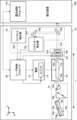
- FIG. 1 schematically shows the configuration of an exposure system in a comparative example.
- FIG. 2 schematically shows the configuration of a laser device according to a comparative example.
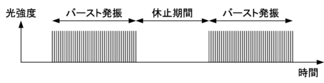
- FIG. 3 is a graph showing an example of output timing of pulsed laser light.
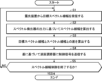
- FIG. 4 is a flowchart showing the procedure of spectral line width control in the comparative example.
- FIG. 5 shows an example of a spectrum waveform for explaining E95.
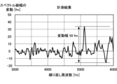
- FIG. 6 shows measurement results of fluctuations in spectral line width according to the repetition frequency of pulsed laser light in a comparative example.
- FIG. 7 shows simulation results of fluctuations in spectral line width according to the repetition frequency of pulsed laser light in a comparative example.
- FIG. 1 schematically shows the configuration of an exposure system in a comparative example.
- FIG. 2 schematically shows the configuration of a laser device according to a comparative example.
- FIG. 3 is a graph showing an example of output timing of pulsed laser light.
- FIG. 4 is a flowchart showing the procedure
- FIG. 8 schematically shows the configuration of the laser device according to the first embodiment.
- FIG. 9 shows the configuration of the band narrowing module in the first embodiment.
- FIG. 10 shows the configuration of the wavefront adjuster in the first embodiment.
- FIG. 11 is a graph showing simulation results of the spectral linewidth of pulsed laser light depending on the g-parameter of the grating and the wavefront adjuster.
- FIG. 12 shows measurement results of fluctuations in spectral line width according to the repetition frequency of pulsed laser light in the first embodiment.
- FIG. 13 shows simulation results of variations in spectral line width according to the repetition frequency of pulsed laser light in the first embodiment.
- FIG. 14 is a graph showing the results of a simulation of the relationship between the g parameter of the grating and the pulse energy.
- FIG. 15 schematically shows the configuration of a laser device in the second embodiment.
- FIG. 16 schematically shows the configuration of a laser device in the third embodiment.
- FIG. 17 shows the power oscillator shown in FIG. 16
- Laser device 1b including master oscillator MO and power oscillator PO 3.1 Configuration 3.2 Operation 3.2.1 Laser control processor 30 3.2.2 Master oscillator MO 3.2.3 Power oscillator PO 3.3 Effect 4. Laser device 1c including a ring resonator 4.1 Configuration 4.2 Operation 4.3 Effect 5. others
- Comparative Example FIG. 1 schematically shows the configuration of an exposure system in a comparative example.
- a comparative example of the present disclosure is a form that the applicant recognizes as being known only by the applicant, and is not a publicly known example that the applicant admits.
- the exposure system includes a laser device 1 and an exposure device 100.
- Laser device 1 includes a laser control processor 30 .
- the laser control processor 30 is a processing device that includes a memory 302 in which a control program is stored, and a CPU (central processing unit) 301 that executes the control program.
- Laser control processor 30 is specifically configured or programmed to perform the various processes included in this disclosure.
- Laser control processor 30 corresponds to the processor in this disclosure.
- the laser device 1 corresponds to a band narrowing laser device in the present disclosure, and is configured to output pulsed laser light toward the exposure device 100.
- the exposure apparatus 100 includes an illumination optical system 101, a projection optical system 102, and an exposure control processor 110.
- Illumination optical system 101 illuminates a reticle pattern of a reticle (not shown) placed on reticle stage RT with pulsed laser light incident from laser device 1 .
- the projection optical system 102 reduces and projects the pulsed laser light that has passed through the reticle, and forms an image on a workpiece (not shown) placed on the workpiece table WT.
- the workpiece is a photosensitive substrate such as a semiconductor wafer coated with a resist film.
- the exposure control processor 110 is a processing device that includes a memory 112 that stores a control program, and a CPU 111 that executes the control program. Exposure control processor 110 is specifically configured or programmed to perform various processes included in this disclosure. The exposure control processor 110 controls the exposure apparatus 100 and transmits and receives various data and signals to and from the laser control processor 30 .
- Exposure Apparatus 100 transmits setting data of the target spectral linewidth and target pulse energy, and a trigger signal to the laser control processor 30.
- Laser control processor 30 controls laser device 1 according to these data and signals.
- Exposure control processor 110 synchronously moves reticle stage RT and workpiece table WT in parallel in opposite directions. As a result, the workpiece is exposed to pulsed laser light that reflects the reticle pattern. The reticle pattern is transferred onto the semiconductor wafer through such an exposure process. After that, an electronic device can be manufactured through a plurality of steps.
- FIG. 2 schematically shows the configuration of a laser device 1 according to a comparative example.
- the laser device 1 includes a laser chamber 10, a discharge electrode 11a, a power supply 12, a band narrowing module 14, a wavefront adjuster 15a, a monitor module 16, and a laser control processor 30.
- the laser device 1 is connectable to an exposure device 100.
- the wavefront adjuster 15a includes an output coupling mirror, and the output coupling mirror and the band narrowing module 14 constitute a laser resonator.
- the laser chamber 10 is placed in the optical path of the laser resonator. Windows 10a and 10b are provided at both ends of the laser chamber 10.
- a discharge electrode 11a and a paired discharge electrode are arranged inside the laser chamber 10.
- a discharge electrode (not shown) is positioned so as to overlap the discharge electrode 11a in the direction of the V axis perpendicular to the paper surface.
- the direction of the V-axis corresponds to the first direction in the present disclosure.
- the laser chamber 10 is filled with a laser gas containing, for example, argon gas or krypton gas as a rare gas, fluorine gas as a halogen gas, and neon gas as a buffer gas.
- the power source 12 includes a switch 13 and is connected to the discharge electrode 11a and a charger (not shown).
- Band narrowing module 14 includes a plurality of prisms 14a and 14b and a grating 14c.
- the prisms 14a and 14b are arranged in this order on the optical path of the light emitted from the window 10a.
- the surfaces of prisms 14a and 14b through which light enters and exits are both parallel to the V-axis.
- the grating 14c is placed in the optical path of the light that has passed through the prisms 14a and 14b.
- the direction of the grooves of the grating 14c is parallel to the V axis.
- the wavefront adjuster 15a includes a cylindrical convex lens 15b and a cylindrical concave lens 15c.
- the cylindrical convex lens 15b is a cylindrical plano-convex lens that includes a flat surface on which a partially reflective film is formed and a convex surface opposite to this flat surface.
- the focal axis of the cylindrical convex lens 15b is parallel to the V-axis.
- the cylindrical concave lens 15c is a cylindrical plano-concave lens that includes a flat surface and a concave surface opposite to the flat surface.
- the focal axis of the cylindrical concave lens 15c is parallel to the V-axis.
- the cylindrical concave lens 15c is supported by a linear stage 15d.
- the linear stage 15d includes an actuator (not shown) that moves the cylindrical concave lens 15c along the optical path of the laser resonator, and a driver (not shown) that drives the actuator in response to a control signal from the laser control processor 30.
- the convex surface of the cylindrical convex lens 15b and the concave surface of the cylindrical concave lens 15c face each other.
- the flat surface of the cylindrical convex lens 15b constitutes an output coupling mirror
- the convex surface of the cylindrical convex lens 15b and the cylindrical concave lens 15c constituting the wavefront adjuster 15a are located between the output coupling mirror and the laser chamber 10.
- the cylindrical convex lens and the output coupling mirror may be composed of separate optical components.
- the wavefront adjuster 15a includes an output coupling mirror that is formed of a flat substrate or a wedge substrate and has a partially reflective film, and a partially reflective film that is located between the output coupling mirror and the laser chamber 10.
- Monitor module 16 The monitor module 16 is located on the optical path of the pulsed laser beam output from the output coupling mirror included in the wavefront adjuster 15a. Monitor module 16 includes beam splitters 16a and 16b, an energy detector 16c, and a spectrum detector 16d.
- the beam splitter 16a is located in the optical path of the pulsed laser beam output from the output coupling mirror.
- the beam splitter 16a is configured to transmit a part of the pulsed laser light toward the exposure apparatus 100 with high transmittance, and reflect the other part.
- Beam splitter 16b is located in the optical path of the pulsed laser beam reflected by beam splitter 16a.
- Energy detector 16c is located in the optical path of the pulsed laser beam reflected by beam splitter 16b.
- the spectrum detector 16d is located on the optical path of the pulsed laser beam that has passed through the beam splitter 16b.
- the spectrum detector 16d includes an etalon and a light distribution sensor (not shown).
- Laser control processor 30 Based on the target pulse energy setting data received from the exposure control processor 110, the laser control processor 30 transmits setting data for the applied voltage to be applied to the discharge electrode 11a to the power source 12. Laser control processor 30 transmits a control signal to linear stage 15d included in wavefront adjuster 15a based on the target spectral linewidth setting data received from exposure control processor 110. Further, the laser control processor 30 transmits an oscillation trigger signal based on the trigger signal received from the exposure control processor 110 to the switch 13 included in the power supply 12.
- Light generated inside the laser chamber 10 is emitted to the outside of the laser chamber 10 via windows 10a and 10b.
- the light emitted from the window 10a of the laser chamber 10 has its beam width expanded by the prisms 14a and 14b, and then enters the grating 14c.
- Light that enters the grating 14c from the prisms 14a and 14b is reflected by the plurality of grooves in the grating 14c, and is diffracted in a direction according to the wavelength of the light.
- Prisms 14a and 14b reduce the beam width of the diffracted light from grating 14c and return the light to laser chamber 10 via window 10a.
- the output coupling mirror included in the wavefront adjuster 15a transmits a part of the light emitted from the window 10b of the laser chamber 10 and outputs it, and reflects the other part and sends it to the laser chamber 10 through the window 10b. Return to inside.
- the light emitted from the laser chamber 10 travels back and forth between the band narrowing module 14 and the output coupling mirror, and is amplified every time it passes through the discharge space inside the laser chamber 10.
- This light is band-narrowed every time it is returned by the band-narrowing module 14.
- the light thus laser oscillated and narrowed in band is output from the output coupling mirror as a pulsed laser light.
- the repetition frequency of the pulsed laser beam is the same as the repetition frequency of the high voltage pulse applied to the discharge electrode 11a, and this repetition frequency changes according to the repetition frequency of the trigger signal received from the exposure apparatus 100.
- Monitor module 16 The energy detector 16c detects the pulse energy of the pulsed laser beam and outputs pulse energy data to the laser control processor 30.
- the pulse energy data is used by the laser control processor 30 to feedback control the setting data of the applied voltage applied to the discharge electrode 11a.
- interference fringes formed by an etalon are measured by a light distribution sensor (not shown), and a fringe waveform representing the light intensity distribution of the interference fringes is generated.
- FIG. 3 is a graph showing an example of output timing of pulsed laser light.
- the laser device 1 performs laser oscillation at a repetition frequency of a certain value or higher over a certain period of time in accordance with a trigger signal from the exposure control processor 110. Performing laser oscillation at a repetition frequency higher than a certain value and outputting pulsed laser light is called "burst oscillation.”
- the laser device 1 stops burst oscillation. Thereafter, the laser device 1 performs burst oscillation again in accordance with the trigger signal from the exposure control processor 110.
- the period between the first burst oscillation and the subsequent second burst oscillation is referred to as a "rest period”.
- the period in which the burst oscillation is performed corresponds to, for example, the period in which one exposure area of the semiconductor wafer is exposed in the exposure apparatus 100.
- the pause period corresponds to, for example, a period in which the imaging position of a reticle pattern is moved from one exposure area to another in the exposure apparatus 100 or a period in which a semiconductor wafer is replaced.
- the linear stage 15d included in the wavefront adjuster 15a controls the laser chamber 10 and the cylindrical convex lens 15b according to the control signal output from the laser control processor 30.
- the cylindrical concave lens 15c is moved along the optical path between.
- the wavefront of the light traveling from the wavefront adjuster 15a to the band narrowing module 14 changes.
- the spectral linewidth of the pulsed laser light changes.
- FIG. 4 is a flowchart showing the procedure of spectral line width control in the comparative example. The process shown in FIG. 4 is executed every time several pulses to several tens of pulses of pulsed laser light are output.
- laser control processor 30 receives a target spectral linewidth from exposure apparatus 100.
- the laser control processor 30 calculates the spectral line width based on the fringe waveform data output from the spectrum detector 16d. Specifically, the laser control processor 30 extracts a portion of the fringe waveform that corresponds to the free spectral range of the etalon. A portion of the waveform extracted from the fringe waveform shows the relationship between the distance from the center of the concentric circles forming the interference fringe and the light intensity. Next, the laser control processor 30 acquires a spectral waveform by coordinately transforming this waveform into a relationship between wavelength and light intensity. Laser control processor 30 calculates the spectral linewidth based on the spectral waveform. The spectral line width may be the full width at half maximum or may be an index called E95.
- FIG. 5 shows an example of a spectrum waveform for explaining E95.
- the horizontal axis in FIG. 5 indicates wavelength, and the vertical axis indicates light intensity.
- the full width of the portion that occupies 95% of the total energy of this spectrum around the center wavelength ⁇ 0 is defined as E95.
- the laser control processor 30 calculates the difference ⁇ between the received target spectral linewidth and the calculated spectral linewidth.
- the laser control processor 30 sends a control signal to the wavefront adjuster 15a based on the difference ⁇ .
- the spectral line width of the pulsed laser beam is feedback-controlled.
- the laser control processor 30 determines whether to end the control of the spectral linewidth. For example, when burst oscillation in which pulsed laser light is output at a constant repetition frequency ends and a rest period begins, control of the spectral line width is ended. When terminating the control of the spectral line width (S5: YES), the laser control processor 30 terminates the processing of this flowchart. If the control of the spectral linewidth is not finished (S5: NO), the laser control processor 30 returns the process to S1 and repeats the above-described operation.
- FIG. 6 shows measurement results of fluctuations in spectral line width according to the repetition frequency of pulsed laser light in a comparative example. Fluctuations in spectral linewidth are measured by the following procedure. First, a first burst oscillation is performed with the repetition frequency of the pulsed laser beam set to 6000 Hz, and the spectral linewidth is controlled using the wavefront adjuster 15a. Thereafter, the control of the spectral line width using the wavefront adjuster 15a is stopped, and the repetition frequency of the pulsed laser beam is set to, for example, 4500 Hz, and a second burst oscillation is performed following the first burst oscillation.
- the difference between the target spectral linewidth in the first burst oscillation and the average value of the spectral linewidths of a predetermined number of pulses from the first pulse in the second burst oscillation is defined as a variation in the spectral linewidth.
- a change in the spectral linewidth is measured by switching to another repetition frequency.
- FIG. 6 it is shown that the spectral line width fluctuated by 50 fm at the maximum due to a change in the repetition frequency of the pulsed laser beam.
- the maximum value of spectral linewidth fluctuation due to a change in repetition frequency is hereinafter referred to as fluctuation width.
- FIG. 7 shows simulation results of fluctuations in spectral line width according to the repetition frequency of pulsed laser light in a comparative example.
- the fluctuation width of the spectral line width due to a change in the repetition frequency of the pulsed laser beam is 59 fm.
- acoustic waves are generated inside the laser chamber 10.
- the acoustic wave is a gas density wave, and when the acoustic wave reaches the optical path of the laser resonator inside the laser chamber 10, a refractive index distribution occurs in the optical path due to the gas density. Due to the refractive index distribution of the optical path, the wavefront of the light toward the band narrowing module 14 changes, and the spectral line width of the pulsed laser light changes.
- the relationship between the timing at which the acoustic wave arrives on the optical path and the timing at which the light passes through depends on the repetition frequency of the pulsed laser beam, so changing the repetition frequency of the pulsed laser beam will change the spectral linewidth of the pulsed laser beam. Conceivable.
- the spectral linewidth is feedback-controlled using the wavefront adjuster 15a, but the spectral linewidth changes significantly at the timing of switching the repetition frequency of the pulsed laser beam, and then the spectral linewidth is controlled by feedback control. It may take time to converge to the target spectral linewidth.
- the repetition frequency of the pulsed laser beam is changed, for example, in the following cases.
- (a) When the repetition frequency of the trigger signal received from the exposure control processor 110 changes (b) When the repetition frequency is changed when aligning the laser device 1 and returned to the original repetition frequency after the alignment is completed (c) ) When changing the repetition frequency when calibrating the laser device 1 and returning to the original repetition frequency after calibration is completed
- the embodiments described below are related to suppressing fluctuations in spectral line width when the repetition frequency of pulsed laser light is changed.
- FIG. 8 schematically shows the configuration of the laser device 1a according to the first embodiment.
- the band narrowing module 14 included in the laser device 1a includes a grating 14c having a concave reflective surface.
- a grating bending mechanism including a holder 14d, an expandable portion 14e, and support portions 14f and 14g may be provided.
- FIG. 9 shows the configuration of the band narrowing module 14 in the first embodiment.
- a holder 14d included in the grating bending mechanism is located opposite the back surface of the grating 14c, and support parts 14f and 14g support both ends of the grating 14c.
- the extensible part 14e located between the support parts 14f and 14g includes, for example, a bolt, and can adjust the curvature of the reflective surface 14h of the grating 14c by adjusting the distance between the central part of the grating 14c and the holder 14d. It is configured. When the interval is narrowed, the reflective surface 14h becomes concave, and when the interval is widened, the reflective surface 14h becomes convex.
- the grating 14c includes a plurality of grooves and ridge lines parallel to the V-axis, and these grooves and ridge lines are arranged alternately in a direction perpendicular to the V-axis.
- the curved surface including these ridgelines that is, the surface of the grating 14c created when all the grooves of the grating 14c are filled, is defined as the reflective surface 14h of the grating 14c.
- the reflective surface 14h may be a part of a cylinder curved in a plane perpendicular to the V-axis, and the radius of this cylinder is defined as the radius of curvature R_Grating.
- the radius of curvature R_Grating of the reflective surface 14h can be calculated from the measurement results obtained by measuring the wavefront of the light diffracted by the grating 14c and directed toward the prism 14b using a wavefront measuring instrument (not shown).
- a wavefront measuring instrument GPI-XP manufactured by Zygo Corporation of the United States can be used.
- g_Grating 1-(L ⁇ M 2 )/(R_Grating ⁇ cos ⁇ )
- the g parameter g_Grating has a value smaller than 1.
- the optical path length L between the principal points of the grating 14c and the wavefront adjuster 15a is 1 ⁇ 10 3 mm
- the beam expansion factor M of the prisms 14a and 14b is 40 times
- the radius of curvature R_Grating of the reflecting surface 14h is 1 ⁇
- the g parameter g_Grating is approximately 0.53.
- the g parameter g_Grating has a value larger than 1.
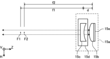
- FIG. 10 shows the configuration of the wavefront adjuster 15a in the first embodiment.
- the focal axis of the cylindrical concave lens 15c is F1
- the focal length is f1
- the focal axis of the cylindrical convex lens 15b is F2
- the focal length is f2
- the distance between the principal points of the cylindrical concave lens 15c and the cylindrical convex lens 15b is d.
- the g parameter g_EFM of the wavefront adjuster 15a is calculated as follows.
- the combined focal length f_EFM1 from the laser chamber 10 to the partially reflective film 15e is as follows.
- f_EFM1 (f1 ⁇ f2)/(f1+f2-d)
- the composite focal length f_EFM2 from the partial reflection film 15e to the laser chamber 10 is the same as the composite focal length f_EFM1.
- f_EFM2 f_EFM1
- the combined focal length f_EFM of the wavefront adjuster 15a is as follows.
- f_EFM (f_EFM1 ⁇ f_EFM1)/(f_EFM1+f_EFM1+ ⁇ 1- ⁇ 2)
- ⁇ 1 is the distance between the cylindrical concave lens 15c and the image-side principal point, and is calculated by the following formula.
- ⁇ 1 f_EFM1 ⁇ d/f2
- ⁇ 2 f_EFM1 ⁇ d/f1
- the g parameter g_EFM has a value smaller than 1.
- the focal length f2 of the cylindrical convex lens 15b is smaller than the sum of the absolute value of the focal length f1 of the cylindrical concave lens 15c and the distance d between the principal points of the cylindrical concave lens 15c and the cylindrical convex lens 15b
- the g parameter g_EFM has a value smaller than 1.
- the focal length f2 is larger than the sum of the absolute value of the focal length f1 and the distance d
- the g parameter g_EFM takes a value larger than 1.
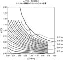
- FIG. 11 is a graph showing the simulation results of the spectral linewidth of pulsed laser light according to the g-parameters g_Grating and g_EFM of the grating 14c and the wavefront adjuster 15a.
- the horizontal axis in FIG. 11 indicates the g parameter g_Grating of the grating 14c, and the vertical axis indicates the g parameter g_EFM of the wavefront adjuster 15a.
- Contours of the spectral linewidth for each combination of these g parameters are shown in the graph. Contour lines are drawn alternately as solid lines and dotted lines every 0.0375 pm.
- the g parameter g_Grating of the grating 14c is 1.
- the g parameter g_Grating is fixed to 1 and the g parameter g_EFM of the wavefront adjuster 15a is changed, the spectral linewidth of the pulsed laser beam changes.
- the reflective surface of the grating 14c is concave, and the g parameter g_Grating of the grating 14c is less than 1.
- the g parameter g_Grating is made smaller than 1, the interval between the contour lines of the spectral linewidth becomes wider. That is, the stability of the spectral linewidth increases when the g parameter g_EFM of the wavefront adjuster 15a is changed. It is thought that the stability of the spectral linewidth is similarly increased when a refractive index distribution occurs in the optical path of the laser resonator due to acoustic waves.
- the spectral line width of the pulsed laser beam can take a value from 0.15 pm to 0.75 pm, but the spectral line width is preferably 0.15 pm or more and 0.5 pm or less.
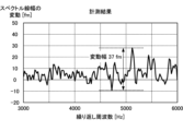
- FIG. 12 shows measurement results of fluctuations in spectral line width according to the repetition frequency of pulsed laser light in the first embodiment.
- the g parameter g_Grating of the grating 14c is set to 0.4.
- FIG. 12 it is shown that the fluctuation width of the spectral line width due to the change in the repetition frequency of the pulsed laser beam was 37 fm.
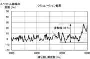
- FIG. 13 shows simulation results of variations in spectral line width according to the repetition frequency of pulsed laser light in the first embodiment.
- the g parameter g_Grating of the grating 14c is set to 0.4.
- the fluctuation width of the spectral line width due to the change in the repetition frequency of the pulsed laser beam is 34 fm.
- FIG. 14 is a graph showing the result of simulating the relationship between the g parameter g_Grating of the grating 14c and pulse energy.
- the target spectral line width when simulating pulse energy was 0.3 pm.
- FIG. 14 also shows the fluctuation range of the spectral line width due to the change in the repetition frequency of the pulsed laser beam.
- the horizontal axis of FIG. 14 shows the g parameter g_Grating of the grating 14c, and the vertical axis shows the relative value of the pulse energy with respect to the pulse energy when g_Grating is set to 1, or the fluctuation width of the spectral line width.
- the pulse energy reaches a peak when the g parameter g_Grating is 0.4 or more and less than 0.5, and the pulse energy becomes low even if the g parameter g_Grating is larger or smaller than that range.
- the pulse energy when the g parameter g_Grating is 0.2 is approximately the same as the pulse energy when the g parameter g_Grating is 1.
- the g parameter g_Grating becomes less than 0.2 or more than 1.0, the proportion of light incident on the wavefront adjuster 15a among the light diffracted by the grating 14c decreases, leaking to the outside of the laser resonator and reducing the pulse energy. is expected to decrease. Therefore, the g parameter g_Grating is preferably 0.2 or more and less than 1.0, more preferably 0.4 or more and less than 0.5.
- the laser device 1a includes a laser resonator, a laser chamber 10, a power source 12, a wavefront adjuster 15a, a spectrum detector 16d, and a laser control processor.
- the laser resonator includes an output coupling mirror constituted by a flat surface of a cylindrical convex lens 15b, and a band narrowing module 14.
- the band narrowing module 14 includes prisms 14a and 14b and a grating 14c.
- the reflective surface 14h is concave.
- the laser chamber 10 includes a discharge electrode 11a and a discharge electrode paired therewith, and is arranged in the optical path of the laser resonator.
- the power source 12 is configured to apply high voltage pulses to the discharge electrode 11a, and the repetition frequency of the high voltage pulses is variable.
- Wavefront adjuster 15a includes an output coupling mirror.
- the spectrum detector 16d generates a fringe waveform to measure the spectral linewidth of the pulsed laser beam output from the output coupling mirror and reflected by the beam splitter 16a.
- Laser control processor 30 controls wavefront adjuster 15a based on the measured spectral linewidth. According to this, by forming the reflective surface 14h into a concave shape, fluctuations in the spectral linewidth due to changes in the repetition frequency of the pulsed laser beam are suppressed, and the spectral linewidth is stabilized.
- the radius of curvature of the reflective surface 14h of the grating 14c is R_Grating
- the incident angle of the light incident on the grating 14c from the prisms 14a and 14b is ⁇
- the wavefront from the principal point of the grating 14c is
- the optical path length to the principal point of the adjuster 15a is L
- the beam expansion rate by the prisms 14a and 14b is M
- g_Grating 1-(L ⁇ M 2 )/(R_Grating ⁇ cos ⁇ )
- the value of g_Grating calculated by the formula is 0.2 or more and less than 1.0. According to this, it is possible to stabilize the spectral line width and suppress a decrease in pulse energy.
- the value of g_Grating is 0.4 or more and less than 0.5. According to this, it is possible to stabilize the spectral line width and obtain high pulse energy.
- the laser control processor 30 g_EFM 1-L/(2 ⁇ f_EFM)
- the wavefront adjuster 15a is controlled so that g_EFM calculated by the equation is larger than the value of g_Grating.
- the target spectral linewidth can be achieved by increasing the g parameter g_EFM of the wavefront adjuster 15a by an amount corresponding to decreasing the g parameter g_Grating of the grating 14c.
- the laser control processor 30 controls the wavefront adjuster 15a so that the spectral line width measured using the spectrum detector 16d is 0.15 pm or more and 0.5 pm or less.
- the g parameter g_Grating of the grating 14c is 0.2 or more and less than 1.0. According to this, by setting the spectral line width to 0.15 pm or more and 0.5 pm or less, and setting the g parameter g_Grating of the grating 14c to 0.2 or more and less than 1.0, the spectral line width is stabilized and the pulse energy can suppress the decline in
- the grating 14c includes a plurality of grooves in the V-axis direction, and the reflective surface 14h has a concave shape curved in a plane perpendicular to the V-axis direction. According to this, the spectral linewidth can be stabilized by adjusting the wavefront shape in a plane perpendicular to the V-axis direction.
- the surface of the prism 14a from which light traveling back and forth in the laser resonator enters the prism 14a and exits from the prism 14a, and the surface of the prism 14b from which light enters the prism 14b and exits from the prism 14b. is parallel to the direction of the V axis. According to this, the beam width in a plane perpendicular to the V-axis direction is expanded by the prisms 14a and 14b, and the beam is made incident on the grating 14c, thereby making it possible to narrow the spectral line width.
- the wavefront adjuster 15a includes the cylindrical convex lens 15b having the focal axis F2 parallel to the V-axis direction and the cylindrical concave lens 15c having the focal axis F1 parallel to the V-axis direction. include. According to this, the spectral linewidth can be controlled by adjusting the wavefront shape in a plane perpendicular to the V-axis direction.
- the wavefront adjuster 15a includes a cylindrical convex lens 15b, a cylindrical concave lens 15c, and a linear stage 15d.
- Cylindrical convex lens 15b includes a flat surface constituting an output coupling mirror and a convex surface located between this flat surface and laser chamber 10.
- the cylindrical concave lens 15c is located on the optical path between the cylindrical convex lens 15b and the laser chamber 10.
- the linear stage 15d moves the cylindrical concave lens 15c. According to this, since the cylindrical concave lens 15c is moved, the wavefront can be adjusted and the spectral linewidth can be controlled without changing the resonator length.
- the band narrowing module 14 includes a grating bending mechanism that includes a holder 14d that adjusts the curvature of the grating 14c, an expandable portion 14e, and support portions 14f and 14g. According to this, the curvature of the reflective surface 14h of the grating 14c can be adjusted to an appropriate value.
- the first embodiment is similar to the comparative example.
- FIG. 15 schematically shows the configuration of a laser device 1b in the second embodiment.
- Laser device 1b includes a master oscillator MO, a power oscillator PO, a monitor module 16, a laser control processor 30, and high reflection mirrors 31 and 32.
- the configuration of the laser control processor 30 is similar to the corresponding configuration in the first embodiment.
- the master oscillator MO includes a laser chamber 10, a discharge electrode 11a, a band narrowing module 14, and a wavefront adjuster 15a. These configurations are similar to the corresponding configurations in the first embodiment, and the reflective surface of the grating 14c included in the band narrowing module 14 is concave.
- FIG. 15 shows a discharge electrode 11b paired with a discharge electrode 11a. In FIG. 15, illustration of the power supply 12 is omitted.
- the high reflection mirrors 31 and 32 are placed in the optical path of the pulsed laser beam B1 output from the master oscillator MO.
- the high reflection mirrors 31 and 32 are configured so that their positions and orientations can be changed by respective actuators (not shown).
- the high reflection mirrors 31 and 32 constitute a beam steering unit for adjusting the incident position and direction of the pulsed laser beam B1 on the power oscillator PO.
- the power oscillator PO is placed in the optical path of the pulsed laser beam B1 that has passed through the beam steering unit.
- Power oscillator PO includes a laser chamber 20, a discharge electrode 21a and a discharge electrode 21b paired therewith, a rear mirror 24, and an output coupling mirror 25.
- the rear mirror 24 is made of a material that transmits the pulsed laser beam B1, and one surface thereof is coated with a partially reflective film. The same applies to the output coupling mirror 25. However, the reflectance of the rear mirror 24 is set higher than the reflectance of the output coupling mirror 25.
- the rear mirror 24 and the output coupling mirror 25 constitute a laser resonator.
- Laser chamber 20 is placed in the optical path of the laser resonator. Windows 20a and 20b are provided at both ends of the laser chamber 20.
- the above-mentioned components of the power oscillator PO are similar to the corresponding components of the master oscillator MO.
- the monitor module 16 is placed in the optical path of the pulsed laser beam B2 output from the output coupling mirror 25.
- the configuration of the monitor module 16 is similar to the corresponding configuration in the first embodiment. In FIG. 15, illustration of the energy detector 16c and beam splitter 16b is omitted.
- Laser control processor 30 receives from exposure control processor 110 setting data for the first target pulse energy of pulsed laser light B2 output from power oscillator PO. Laser control processor 30 further sets a second target pulse energy of pulsed laser light B1 output from master oscillator MO.
- Laser control processor 30 transmits setting data for applied voltages to the respective power supplies of master oscillator MO and power oscillator PO based on the first and second target pulse energies. Laser control processor 30 transmits first and second oscillation trigger signals based on the trigger signal received from exposure control processor 110 to switches included in the power supplies of master oscillator MO and power oscillator PO, respectively.
- the power source included in the master oscillator MO is connected so that the timing at which discharge occurs inside the laser chamber 20 and the timing at which the pulsed laser beam B1 outputted from the master oscillator MO enters the inside of the laser chamber 20 are synchronized.
- a delay time of the second oscillation trigger signal to the power supply included in the power oscillator PO with respect to the first oscillation trigger signal is set.
- the pulsed laser beam B1 reciprocates between the rear mirror 24 and the output coupling mirror 25, and is amplified every time it passes through the discharge space inside the laser chamber 20.
- the amplified pulsed laser beam B2 is output from the output coupling mirror 25.
- the second embodiment by amplifying the pulsed laser beam B1 output from the master oscillator MO, it is possible to output the pulsed laser beam B2 having high pulse energy toward the exposure apparatus 100. can.
- the spectral linewidth of the pulsed laser beam B2 depends on the spectral linewidth of the pulsed laser beam B1.
- the second embodiment is similar to the first embodiment.
- FIG. 16 schematically shows the configuration of a laser device 1c in the third embodiment.
- FIG. 17 shows the power oscillator PO shown in FIG. 16 viewed from a different direction from that shown in FIG.
- Laser device 1c includes a master oscillator MO, a power oscillator PO, a monitor module 16, a laser control processor 30, and high reflection mirrors 31 and 32.
- the configuration of the master oscillator MO is similar to the corresponding configuration in the second embodiment, and the reflective surface of the grating 14c included in the band narrowing module 14 is concave.
- Power oscillator PO includes a laser chamber 20, high reflection mirrors 26a to 26c, an output coupling mirror 27, and a high reflection mirror 33.
- the configurations of the laser chamber 20, the windows 20a and 20b provided therein, and the pair of discharge electrodes 21a and 21b are similar to the corresponding configurations in the second embodiment.
- the output coupling mirror 27 and the high reflection mirror 26a are arranged outside the laser chamber 20 and near the window 20a.
- High reflective mirrors 26b and 26c are located outside of laser chamber 20 and near window 20b.
- a laser resonator composed of the high reflection mirrors 26a to 26c and the output coupling mirror 27 is called a ring resonator.
- the pulsed laser beam B1 output from the master oscillator MO is reflected by the high reflection mirrors 31, 32, and 33 in this order, and is reflected from the outside of the laser resonator of the power oscillator PO to the output coupling mirror 27 by approximately - It is incident in the H direction.
- the pulsed laser beam B1 that enters the laser resonator via the output coupling mirror 27 is reflected by the high reflection mirrors 26a, 26b, and 26c in this order, is amplified when passing through the discharge space, and is reflected in the laser resonator.
- the light enters the output coupling mirror 27 from the inside in the Z direction.
- a part of the pulsed laser beam B1 incident on the output coupling mirror 27 in the Z direction is reflected approximately in the -H direction, and is again reflected and amplified by the high reflection mirrors 26a, 26b, and 26c.
- the other part of the pulsed laser beam B1 incident on the output coupling mirror 27 in the Z direction is transmitted and output toward the exposure apparatus 100 as a pulsed laser beam B2.
- the third embodiment since return light from the power oscillator PO toward the master oscillator MO is less likely to occur, the master oscillator MO can be stably operated.
- the third embodiment is similar to the second embodiment.
Landscapes
- Physics & Mathematics (AREA)
- Electromagnetism (AREA)
- Engineering & Computer Science (AREA)
- Plasma & Fusion (AREA)
- Optics & Photonics (AREA)
- Automation & Control Theory (AREA)
- General Physics & Mathematics (AREA)
- Lasers (AREA)
Abstract
Description
1.比較例
1.1 露光装置100の構成
1.2 露光装置100の動作
1.3 レーザ装置1の構成
1.3.1 レーザ共振器
1.3.2 モニタモジュール16
1.4 レーザ装置1の動作
1.4.1 レーザ制御プロセッサ30
1.4.2 レーザ発振
1.4.3 モニタモジュール16
1.4.4 バースト発振
1.4.5 スペクトル線幅制御
1.5 比較例の課題
2.凹面状のグレーティング14cを含むレーザ装置1a
2.1 構成
2.2 グレーティング14cのgパラメータg_Grating
2.3 波面調節器15aのgパラメータg_EFM
2.4 gパラメータとスペクトル線幅との関係
2.5 gパラメータとパルスエネルギーとの関係
2.6 作用
3.マスターオシレータMO及びパワーオシレータPOを含むレーザ装置1b
3.1 構成
3.2 動作
3.2.1 レーザ制御プロセッサ30
3.2.2 マスターオシレータMO
3.2.3 パワーオシレータPO
3.3 作用
4.リング共振器を含むレーザ装置1c
4.1 構成
4.2 動作
4.3 作用
5.その他
図1は、比較例における露光システムの構成を概略的に示す。本開示の比較例とは、出願人のみによって知られていると出願人が認識している形態であって、出願人が自認している公知例ではない。
露光装置100は、照明光学系101と、投影光学系102と、露光制御プロセッサ110と、を含む。
照明光学系101は、レーザ装置1から入射したパルスレーザ光によって、レチクルステージRT上に配置された図示しないレチクルのレチクルパターンを照明する。
投影光学系102は、レチクルを透過したパルスレーザ光を、縮小投影してワークピーステーブルWT上に配置された図示しないワークピースに結像させる。ワークピースはレジスト膜が塗布された半導体ウエハ等の感光基板である。
露光制御プロセッサ110は、目標スペクトル線幅及び目標パルスエネルギーの設定データ、及びトリガ信号をレーザ制御プロセッサ30に送信する。レーザ制御プロセッサ30は、これらのデータ及び信号に従ってレーザ装置1を制御する。
露光制御プロセッサ110は、レチクルステージRTとワークピーステーブルWTとを同期して互いに逆方向に平行移動させる。これにより、レチクルパターンを反映したパルスレーザ光でワークピースが露光される。
このような露光工程によって半導体ウエハにレチクルパターンが転写される。その後、複数の工程を経ることで電子デバイスを製造することができる。
図2は、比較例に係るレーザ装置1の構成を概略的に示す。レーザ装置1は、レーザチャンバ10と、放電電極11aと、電源12と、狭帯域化モジュール14と、波面調節器15aと、モニタモジュール16と、レーザ制御プロセッサ30と、を含む。レーザ装置1は露光装置100に接続可能とされている。
波面調節器15aは出力結合ミラーを含み、この出力結合ミラーと狭帯域化モジュール14とで、レーザ共振器が構成される。レーザチャンバ10は、レーザ共振器の光路に配置されている。レーザチャンバ10の両端にはウインドウ10a及び10bが設けられている。レーザチャンバ10の内部に、放電電極11a及びこれと対をなす図示しない放電電極が配置されている。図示しない放電電極は、紙面に垂直なV軸の方向において放電電極11aと重なるように位置している。V軸の方向は本開示における第1方向に相当する。レーザチャンバ10には、例えばレアガスとしてアルゴンガス又はクリプトンガス、ハロゲンガスとしてフッ素ガス、バッファガスとしてネオンガス等を含むレーザガスが封入される。
電源12は、スイッチ13を含むとともに、放電電極11aと図示しない充電器とに接続されている。
グレーティング14cは、プリズム14a及び14bを透過した光の光路に配置されている。グレーティング14cの溝の方向は、V軸に平行である。
シリンドリカル凸レンズ15bは、部分反射膜が形成された平らな表面と、この表面と反対側の凸面と、を含むシリンドリカル平凸レンズである。シリンドリカル凸レンズ15bの焦点軸はV軸に平行である。
シリンドリカル凹レンズ15cは、平らな表面と、この表面と反対側の凹面と、を含むシリンドリカル平凹レンズである。シリンドリカル凹レンズ15cの焦点軸はV軸に平行である。シリンドリカル凹レンズ15cは、リニアステージ15dに支持されている。リニアステージ15dは、シリンドリカル凹レンズ15cをレーザ共振器の光路に沿って移動させる図示しないアクチュエータと、レーザ制御プロセッサ30からの制御信号に応じてアクチュエータを駆動する図示しないドライバと、を含む。
ここではシリンドリカル凸レンズ15bの平らな表面が出力結合ミラーを構成する場合について説明したが、シリンドリカル凸レンズと出力結合ミラーとは別々の光学部品で構成されてもよい。すなわち、波面調節器15aは、シリンドリカル凸レンズ15bの代わりに、平面基板又はウェッジ基板で構成され部分反射膜を有する出力結合ミラーと、この出力結合ミラーとレーザチャンバ10との間に位置し部分反射膜を有しないシリンドリカル凸レンズと、を含んでもよい。
モニタモジュール16は、波面調節器15aに含まれる出力結合ミラーから出力されたパルスレーザ光の光路に位置する。モニタモジュール16は、ビームスプリッタ16a及び16bと、エネルギー検出器16cと、スペクトル検出器16dと、を含む。
1.4.1 レーザ制御プロセッサ30
レーザ制御プロセッサ30は、露光制御プロセッサ110から受信した目標パルスエネルギーの設定データに基づいて、放電電極11aに印加される印加電圧の設定データを電源12に送信する。レーザ制御プロセッサ30は、露光制御プロセッサ110から受信した目標スペクトル線幅の設定データに基づいて、波面調節器15aに含まれるリニアステージ15dに制御信号を送信する。また、レーザ制御プロセッサ30は、露光制御プロセッサ110から受信したトリガ信号に基づく発振トリガ信号を電源12に含まれるスイッチ13に送信する。
スイッチ13は、レーザ制御プロセッサ30から発振トリガ信号を受信するとオン状態となる。電源12は、スイッチ13がオン状態となると、図示しない充電器に充電された電気エネルギーから高電圧パルスを生成し、この高電圧パルスを放電電極11aに印加する。
プリズム14a及び14bからグレーティング14cに入射した光は、グレーティング14cの複数の溝によって反射されるとともに、光の波長に応じた方向に回折させられる。
波面調節器15aに含まれる出力結合ミラーは、レーザチャンバ10のウインドウ10bから出射した光のうちの一部を透過させて出力し、他の一部を反射してウインドウ10bを介してレーザチャンバ10の内部に戻す。
エネルギー検出器16cは、パルスレーザ光のパルスエネルギーを検出し、パルスエネルギーのデータをレーザ制御プロセッサ30に出力する。パルスエネルギーのデータは、レーザ制御プロセッサ30が放電電極11aに印加される印加電圧の設定データをフィードバック制御するのに用いられる。
図3は、パルスレーザ光の出力タイミングの例を示すグラフである。レーザ装置1は、露光制御プロセッサ110からのトリガ信号に従い、ある期間にわたって一定値以上の繰り返し周波数でレーザ発振を行う。一定値以上の繰り返し周波数でレーザ発振を行い、パルスレーザ光を出力することを「バースト発振」という。
図2を再び参照し、波面調節器15aに含まれるリニアステージ15dは、レーザ制御プロセッサ30から出力される制御信号に応じて、レーザチャンバ10とシリンドリカル凸レンズ15bとの間の光路に沿ってシリンドリカル凹レンズ15cを移動させる。これにより、波面調節器15aから狭帯域化モジュール14へ向かう光の波面が変化する。波面が変化することにより、パルスレーザ光のスペクトル線幅が変化する。
S1において、レーザ制御プロセッサ30は、露光装置100から目標スペクトル線幅を受信する。
具体的には、レーザ制御プロセッサ30は、フリンジ波形のうちのエタロンのフリースペクトラルレンジに相当する一部分の波形を抽出する。フリンジ波形から抽出された一部分の波形は、干渉縞を構成する同心円の中心からの距離と光強度との関係を示している。次に、レーザ制御プロセッサ30は、この波形を、波長と光強度との関係に座標変換することにより、スペクトル波形を取得する。レーザ制御プロセッサ30は、スペクトル波形に基づいてスペクトル線幅を算出する。スペクトル線幅は、半値全幅でもよいし、E95と呼ばれる指標でもよい。
S4において、レーザ制御プロセッサ30は、差ΔΔλに基づいて波面調節器15aに制御信号を送信する。これにより、パルスレーザ光のスペクトル線幅がフィードバック制御される。
図6は、比較例におけるパルスレーザ光の繰り返し周波数に応じたスペクトル線幅の変動の計測結果を示す。スペクトル線幅の変動は、以下の手順により計測される。まず、パルスレーザ光の繰り返し周波数を6000Hzとして第1のバースト発振を行い、波面調節器15aを用いたスペクトル線幅の制御を行う。その後、波面調節器15aを用いたスペクトル線幅の制御を中止し、パルスレーザ光の繰り返し周波数を例えば4500Hzとして第1のバースト発振の次の第2のバースト発振を行う。第1のバースト発振における目標スペクトル線幅と、第2のバースト発振における最初のパルスから所定数のパルスのスペクトル線幅の平均値との差をスペクトル線幅の変動とする。同様に、繰り返し周波数を6000Hzとして第1のバースト発振を行った後、他の繰り返し周波数に切り替えてスペクトル線幅の変動を計測する。
図7においては、パルスレーザ光の繰り返し周波数の変化によるスペクトル線幅の変動幅が59fmであることが示されている。
(a)露光制御プロセッサ110から受信するトリガ信号の繰り返し周波数が変わった場合
(b)レーザ装置1のアライメントを行う際に繰り返し周波数を変更し、アライメントの終了後に元の繰り返し周波数に戻す場合
(c)レーザ装置1のキャリブレーションを行う際に繰り返し周波数を変更し、キャリブレーションの終了後に元の繰り返し周波数に戻す場合
2.1 構成
図8は、第1の実施形態に係るレーザ装置1aの構成を概略的に示す。レーザ装置1aに含まれる狭帯域化モジュール14は、凹面状の反射面を有するグレーティング14cを含む。グレーティング14cの反射面の形状を調整するために、ホルダ14d、伸縮部14e、支持部14f及び14gを含むグレーティング曲げ機構が設けられてもよい。
M=w2/w1
プリズム14bからグレーティング14cに入射する光の入射角をθとする。グレーティング14cと波面調節器15aとの主点間の光路長をLとする(図8参照)。このとき、グレーティング14cのgパラメータg_Gratingは以下の式で定義される。
g_Grating=1-(L×M2)/(R_Grating×cosθ)
反射面14hが凸面であるとき、gパラメータg_Gratingは1より大きい値となる。
図10は、第1の実施形態における波面調節器15aの構成を示す。シリンドリカル凹レンズ15cの焦点軸をF1、焦点距離をf1とし、シリンドリカル凸レンズ15bの焦点軸をF2、焦点距離をf2とし、シリンドリカル凹レンズ15cとシリンドリカル凸レンズ15bとの主点間の距離をdとする。波面調節器15aのgパラメータg_EFMは以下のように算出される。
f_EFM1=(f1×f2)/(f1+f2-d)
部分反射膜15eからレーザチャンバ10までの合成焦点距離f_EFM2は合成焦点距離f_EFM1と同じである。
f_EFM2=f_EFM1
f_EFM=(f_EFM1×f_EFM1)/(f_EFM1+f_EFM1+δ1-δ2)
ここで、δ1はシリンドリカル凹レンズ15cと像側主点との距離であり、以下の式で算出される。
δ1=f_EFM1×d/f2
δ2はシリンドリカル凸レンズ15bと物側主点との距離であり、以下の式で算出される。
δ2=f_EFM1×d/f1
g_EFM=1-L/(2×f_EFM)
焦点距離f1の絶対値と距離dとの和より焦点距離f2が大きいとき、gパラメータg_EFMは1より大きい値となる。
図11は、グレーティング14c及び波面調節器15aのgパラメータg_Grating及びg_EFMに応じたパルスレーザ光のスペクトル線幅のシミュレーション結果を示すグラフである。図11の横軸はグレーティング14cのgパラメータg_Gratingを示し、縦軸は波面調節器15aのgパラメータg_EFMを示す。これらのgパラメータの組み合わせごとのスペクトル線幅の等高線がグラフに示されている。等高線は0.0375pmごとに実線と点線とで交互に描かれている。
図12においては、パルスレーザ光の繰り返し周波数の変化によるスペクトル線幅の変動幅が37fmであったことが示されている。
図13においては、パルスレーザ光の繰り返し周波数の変化によるスペクトル線幅の変動幅が34fmであることが示されている。
図14は、グレーティング14cのgパラメータg_Gratingとパルスエネルギーとの関係をシミュレーションした結果を示すグラフである。パルスエネルギーをシミュレーションする際の目標スペクトル線幅は0.3pmとした。図14には、パルスレーザ光の繰り返し周波数の変化によるスペクトル線幅の変動幅が併せて示されている。図14の横軸はグレーティング14cのgパラメータg_Gratingを示し、縦軸はg_Gratingを1としたときのパルスエネルギーを基準としたパルスエネルギーの相対値、あるいは、スペクトル線幅の変動幅を示す。
但し、gパラメータg_Gratingが0.4以上0.5未満でパルスエネルギーはピークとなり、gパラメータg_Gratingがその範囲よりも大きくても小さくてもパルスエネルギーが低くなる。gパラメータg_Gratingが0.2である場合のパルスエネルギーは、gパラメータg_Gratingが1である場合のパルスエネルギーとほぼ同じとなる。gパラメータg_Gratingが0.2未満又は1.0以上となると、グレーティング14cによって回折された光のうちの波面調節器15aに入射する光の割合が低下し、レーザ共振器の外部に漏れてパルスエネルギーが低下すると考えられる。従って、gパラメータg_Gratingは0.2以上1.0未満が好ましく、0.4以上0.5未満がより好ましい。
(1)第1の実施形態によれば、レーザ装置1aは、レーザ共振器と、レーザチャンバ10と、電源12と、波面調節器15aと、スペクトル検出器16dと、レーザ制御プロセッサ30と、を含む。
レーザ共振器は、シリンドリカル凸レンズ15bの平らな表面で構成される出力結合ミラーと、狭帯域化モジュール14と、を含み、狭帯域化モジュール14はプリズム14a及び14bとグレーティング14cとを含み、グレーティング14cの反射面14hは凹面状である。
レーザチャンバ10は、放電電極11a及びこれと対をなす放電電極を含み、レーザ共振器の光路に配置される。
電源12は、放電電極11aに高電圧パルスを印加するように構成され、高電圧パルスの繰り返し周波数は可変である。
波面調節器15aは、出力結合ミラーを含む。
スペクトル検出器16dは、出力結合ミラーから出力され、ビームスプリッタ16aによって反射されたパルスレーザ光のスペクトル線幅を計測するためにフリンジ波形を生成する。
レーザ制御プロセッサ30は、計測されたスペクトル線幅に基づいて波面調節器15aを制御する。
これによれば、反射面14hを凹面状としたことで、パルスレーザ光の繰り返し周波数の変化によるスペクトル線幅の変動が抑制され、スペクトル線幅が安定化する。
g_Grating=1-(L×M2)/(R_Grating×cosθ)
の式で算出されるg_Gratingの値が0.2以上1.0未満である。
これによれば、スペクトル線幅を安定化するとともに、パルスエネルギーの低下を抑制し得る。
これによれば、スペクトル線幅を安定化するとともに、高いパルスエネルギーを得ることができる。
g_EFM=1-L/(2×f_EFM)
の式で算出されるg_EFMがg_Gratingの値より大きい値となるように波面調節器15aを制御する。
これによれば、グレーティング14cのgパラメータg_Gratingを小さくする分だけ波面調節器15aのgパラメータg_EFMを大きくすることで、目標スペクトル線幅を実現し得る。
これによれば、スペクトル線幅を0.15pm以上0.5pm以下とし、グレーティング14cのgパラメータg_Gratingを0.2以上1.0未満とすることで、スペクトル線幅が安定化するとともに、パルスエネルギーの低下を抑制し得る。
これによれば、V軸の方向に垂直な面内の波面形状を調整することで、スペクトル線幅を安定化できる。
これによれば、プリズム14a及び14bによりV軸の方向に垂直な面内のビーム幅を拡大してグレーティング14cに入射させることで、スペクトル線幅を狭帯域化できる。
これによれば、V軸の方向に垂直な面内の波面形状を調整することで、スペクトル線幅を制御できる。
これによれば、シリンドリカル凹レンズ15cを移動させるので、共振器長を変化させることなく波面を調整してスペクトル線幅を制御できる。
これによれば、グレーティング14cの反射面14hの曲率を適切な値に調整し得る。
他の点については、第1の実施形態は比較例と同様である。
3.1 構成
図15は、第2の実施形態におけるレーザ装置1bの構成を概略的に示す。レーザ装置1bは、マスターオシレータMOと、パワーオシレータPOと、モニタモジュール16と、レーザ制御プロセッサ30と、高反射ミラー31及び32と、を含む。レーザ制御プロセッサ30の構成は第1の実施形態において対応する構成と同様である。
3.2.1 レーザ制御プロセッサ30
レーザ制御プロセッサ30は、パワーオシレータPOから出力されるパルスレーザ光B2の第1の目標パルスエネルギーの設定データを露光制御プロセッサ110から受信する。
レーザ制御プロセッサ30は、さらに、マスターオシレータMOから出力されるパルスレーザ光B1の第2の目標パルスエネルギーを設定する。
レーザ制御プロセッサ30は、露光制御プロセッサ110から受信したトリガ信号に基づく第1及び第2の発振トリガ信号をマスターオシレータMO及びパワーオシレータPOそれぞれの電源に含まれるスイッチに送信する。
マスターオシレータMOの動作は、第1の実施形態におけるレーザ装置1aの動作と同様である。
パワーオシレータPOに含まれる電源は、レーザ制御プロセッサ30から第2の発振トリガ信号を受信すると高電圧パルスを生成し、この高電圧パルスを放電電極21aに印加する。
第2の実施形態によれば、マスターオシレータMOから出力されたパルスレーザ光B1を増幅することにより、高いパルスエネルギーを有するパルスレーザ光B2を露光装置100に向けて出力することができる。
パルスレーザ光B2のスペクトル線幅はパルスレーザ光B1のスペクトル線幅に依存する。グレーティング14cの反射面を凹面状とすることで、パルスレーザ光B2のスペクトル線幅を安定化し得る。
他の点については、第2の実施形態は第1の実施形態と同様である。
4.1 構成
図16は、第3の実施形態におけるレーザ装置1cの構成を概略的に示す。図17は、図16に示されるパワーオシレータPOを図16と異なる方向から見た様子を示す。レーザ装置1cは、マスターオシレータMOと、パワーオシレータPOと、モニタモジュール16と、レーザ制御プロセッサ30と、高反射ミラー31及び32と、を含む。マスターオシレータMOの構成は第2の実施形態において対応する構成と同様であり、狭帯域化モジュール14に含まれるグレーティング14cの反射面は凹面状である。
マスターオシレータMOから出力されたパルスレーザ光B1は、高反射ミラー31、32、及び33によってこの順で反射され、パワーオシレータPOのレーザ共振器の外側から出力結合ミラー27にほぼ-H方向に入射する。出力結合ミラー27を介してレーザ共振器に入射したパルスレーザ光B1は、高反射ミラー26a、26b、及び26cによってこの順で反射され、放電空間を通過する際に増幅されて、レーザ共振器の内側から出力結合ミラー27にZ方向に入射する。
第3の実施形態によれば、パワーオシレータPOからマスターオシレータMOへ向かう戻り光が発生しにくいため、マスターオシレータMOを安定して動作させることができる。
他の点については、第3の実施形態は第2の実施形態と同様である。
上述の説明は、制限ではなく単なる例示を意図している。従って、特許請求の範囲を逸脱することなく本開示の実施形態に変更を加えることができることは、当業者には明らかである。また、本開示の実施形態を組み合わせて使用することも当業者には明らかである。
Claims (20)
- 出力結合ミラー及び狭帯域化モジュールを含むレーザ共振器であって、前記狭帯域化モジュールがプリズム及びグレーティングを含み、前記グレーティングの反射面が凹面状である、前記レーザ共振器と、
一対の放電電極を含み、前記レーザ共振器の光路に配置されたレーザチャンバと、
前記放電電極に高電圧パルスを印加する電源であって、前記高電圧パルスの繰り返し周波数が可変である前記電源と、
前記出力結合ミラーを含む波面調節器と、
前記出力結合ミラーから出力されたパルスレーザ光のスペクトル線幅を計測するためのスペクトル検出器と、
前記計測されたスペクトル線幅に基づいて前記波面調節器を制御するプロセッサと、
を備える狭帯域化レーザ装置。 - 請求項1記載の狭帯域化レーザ装置であって、
前記グレーティングの反射面の曲率半径をR_Gratingとし、前記プリズムから前記グレーティングに入射する光の入射角をθとし、前記グレーティングの主点から前記波面調節器の主点までの光路長をLとし、前記プリズムによるビーム拡大率をMとしたとき、
g_Grating=1-(L×M2)/(R_Grating×cosθ)
の式で算出されるg_Gratingの値が0.2以上1.0未満である、
狭帯域化レーザ装置。 - 請求項2記載の狭帯域化レーザ装置であって、
前記g_Gratingの値が0.4以上0.5未満である、
狭帯域化レーザ装置。 - 請求項2記載の狭帯域化レーザ装置であって、
前記波面調節器の合成焦点距離をf_EFMとしたとき、前記プロセッサは、
g_EFM=1-L/(2×f_EFM)
の式で算出されるg_EFMが前記g_Gratingの値より大きい値となるように前記波面調節器を制御する、
狭帯域化レーザ装置。 - 請求項2記載の狭帯域化レーザ装置であって、
前記プロセッサは、前記計測されるスペクトル線幅が0.15pm以上0.5pm以下となるように前記波面調節器を制御する、
狭帯域化レーザ装置。 - 請求項1記載の狭帯域化レーザ装置であって、
前記グレーティングは、第1方向の複数の溝を含み、前記反射面は、前記第1方向に垂直な面内に湾曲した凹面状である、
狭帯域化レーザ装置。 - 請求項6記載の狭帯域化レーザ装置であって、
前記レーザ共振器を往復する光が前記プリズムに入射及び前記プリズムから出射する前記プリズムの表面は、前記第1方向に平行である、
狭帯域化レーザ装置。 - 請求項6記載の狭帯域化レーザ装置であって、
前記波面調節器は、それぞれ前記第1方向に平行な焦点軸を有するシリンドリカル凸レンズ及びシリンドリカル凹レンズを含む、
狭帯域化レーザ装置。 - 請求項1記載の狭帯域化レーザ装置であって、
前記波面調節器は、
前記出力結合ミラーを構成する平らな表面と、前記平らな表面と前記レーザチャンバとの間に位置する凸面と、を含むシリンドリカル平凸レンズと、
前記シリンドリカル平凸レンズと前記レーザチャンバとの間の光路に位置するシリンドリカル凹レンズと、
前記シリンドリカル凹レンズを移動させるアクチュエータと、
を含む、狭帯域化レーザ装置。 - 請求項1記載の狭帯域化レーザ装置であって、
前記狭帯域化モジュールは、前記グレーティングの曲率を調整するグレーティング曲げ機構を含む、
狭帯域化レーザ装置。 - 電子デバイスの製造方法であって、
出力結合ミラー及び狭帯域化モジュールを含むレーザ共振器であって、前記狭帯域化モジュールがプリズム及びグレーティングを含み、前記グレーティングの反射面が凹面状である、前記レーザ共振器と、
一対の放電電極を含み、前記レーザ共振器の光路に配置されたレーザチャンバと、
前記放電電極に高電圧パルスを印加する電源であって、前記高電圧パルスの繰り返し周波数が可変である前記電源と、
前記出力結合ミラーを含む波面調節器と、
前記出力結合ミラーから出力されたパルスレーザ光のスペクトル線幅を計測するためのスペクトル検出器と、
前記計測されたスペクトル線幅に基づいて前記波面調節器を制御するプロセッサと、
を備える狭帯域化レーザ装置によって前記パルスレーザ光を生成し、
前記パルスレーザ光を露光装置に出力し、
前記電子デバイスを製造するために、前記露光装置内で感光基板上に前記パルスレーザ光を露光する
ことを含む電子デバイスの製造方法。 - 請求項11記載の電子デバイスの製造方法であって、
前記グレーティングの反射面の曲率半径をR_Gratingとし、前記プリズムから前記グレーティングに入射する光の入射角をθとし、前記グレーティングの主点から前記波面調節器の主点までの光路長をLとし、前記プリズムによるビーム拡大率をMとしたとき、
g_Grating=1-(L×M2)/(R_Grating×cosθ)
の式で算出されるg_Gratingの値が0.2以上1.0未満である、
電子デバイスの製造方法。 - 請求項12記載の電子デバイスの製造方法であって、
前記g_Gratingの値が0.4以上0.5未満である、
電子デバイスの製造方法。 - 請求項12記載の電子デバイスの製造方法であって、
前記波面調節器の合成焦点距離をf_EFMとしたとき、前記プロセッサは、
g_EFM=1-L/(2×f_EFM)
の式で算出されるg_EFMが前記g_Gratingの値より大きい値となるように前記波面調節器を制御する、
電子デバイスの製造方法。 - 請求項12記載の電子デバイスの製造方法であって、
前記プロセッサは、前記計測されるスペクトル線幅が0.15pm以上0.5pm以下となるように前記波面調節器を制御する、
電子デバイスの製造方法。 - 請求項11記載の電子デバイスの製造方法であって、
前記グレーティングは、第1方向の複数の溝を含み、前記反射面は、前記第1方向に垂直な面内に湾曲した凹面状である、
電子デバイスの製造方法。 - 請求項16記載の電子デバイスの製造方法であって、
前記レーザ共振器を往復する光が前記プリズムに入射及び前記プリズムから出射する前記プリズムの表面は、前記第1方向に平行である、
電子デバイスの製造方法。 - 請求項16記載の電子デバイスの製造方法であって、
前記波面調節器は、それぞれ前記第1方向に平行な焦点軸を有するシリンドリカル凸レンズ及びシリンドリカル凹レンズを含む、
電子デバイスの製造方法。 - 請求項11記載の電子デバイスの製造方法であって、
前記波面調節器は、
前記出力結合ミラーを構成する平らな表面と、前記平らな表面と前記レーザチャンバとの間に位置する凸面と、を含むシリンドリカル平凸レンズと、
前記シリンドリカル平凸レンズと前記レーザチャンバとの間の光路に位置するシリンドリカル凹レンズと、
前記シリンドリカル凹レンズを移動させるアクチュエータと、
を含む、電子デバイスの製造方法。 - 請求項11記載の電子デバイスの製造方法であって、
前記狭帯域化モジュールは、前記グレーティングの曲率を調整するグレーティング曲げ機構を含む、
電子デバイスの製造方法。
Priority Applications (4)
| Application Number | Priority Date | Filing Date | Title |
|---|---|---|---|
| CN202280098841.3A CN119654750A (zh) | 2022-09-02 | 2022-09-02 | 窄带化激光装置以及电子器件的制造方法 |
| PCT/JP2022/033143 WO2024047871A1 (ja) | 2022-09-02 | 2022-09-02 | 狭帯域化レーザ装置、及び電子デバイスの製造方法 |
| JP2024543749A JPWO2024047871A1 (ja) | 2022-09-02 | 2022-09-02 | |
| US19/040,321 US20250174960A1 (en) | 2022-09-02 | 2025-01-29 | Line narrowing laser device, and electronic device manufacturing method |
Applications Claiming Priority (1)
| Application Number | Priority Date | Filing Date | Title |
|---|---|---|---|
| PCT/JP2022/033143 WO2024047871A1 (ja) | 2022-09-02 | 2022-09-02 | 狭帯域化レーザ装置、及び電子デバイスの製造方法 |
Related Child Applications (1)
| Application Number | Title | Priority Date | Filing Date |
|---|---|---|---|
| US19/040,321 Continuation US20250174960A1 (en) | 2022-09-02 | 2025-01-29 | Line narrowing laser device, and electronic device manufacturing method |
Publications (1)
| Publication Number | Publication Date |
|---|---|
| WO2024047871A1 true WO2024047871A1 (ja) | 2024-03-07 |
Family
ID=90099081
Family Applications (1)
| Application Number | Title | Priority Date | Filing Date |
|---|---|---|---|
| PCT/JP2022/033143 Ceased WO2024047871A1 (ja) | 2022-09-02 | 2022-09-02 | 狭帯域化レーザ装置、及び電子デバイスの製造方法 |
Country Status (4)
| Country | Link |
|---|---|
| US (1) | US20250174960A1 (ja) |
| JP (1) | JPWO2024047871A1 (ja) |
| CN (1) | CN119654750A (ja) |
| WO (1) | WO2024047871A1 (ja) |
Citations (6)
| Publication number | Priority date | Publication date | Assignee | Title |
|---|---|---|---|---|
| JPH0427182A (ja) * | 1990-05-22 | 1992-01-30 | Mitsubishi Electric Corp | パルスレーザ装置 |
| US5095492A (en) * | 1990-07-17 | 1992-03-10 | Cymer Laser Technologies | Spectral narrowing technique |
| JPH1126856A (ja) * | 1997-06-30 | 1999-01-29 | Komatsu Ltd | 反射型波長選択素子の曲げ機構 |
| JPH11274632A (ja) * | 1998-03-25 | 1999-10-08 | Komatsu Ltd | 狭帯域化レーザの波面制御装置 |
| JP2008016544A (ja) * | 2006-07-04 | 2008-01-24 | Komatsu Ltd | 狭帯域化レーザのスペクトル幅調整方法 |
| WO2022085146A1 (ja) * | 2020-10-22 | 2022-04-28 | ギガフォトン株式会社 | レーザ装置、及び電子デバイスの製造方法 |
-
2022
- 2022-09-02 WO PCT/JP2022/033143 patent/WO2024047871A1/ja not_active Ceased
- 2022-09-02 CN CN202280098841.3A patent/CN119654750A/zh active Pending
- 2022-09-02 JP JP2024543749A patent/JPWO2024047871A1/ja active Pending
-
2025
- 2025-01-29 US US19/040,321 patent/US20250174960A1/en active Pending
Patent Citations (6)
| Publication number | Priority date | Publication date | Assignee | Title |
|---|---|---|---|---|
| JPH0427182A (ja) * | 1990-05-22 | 1992-01-30 | Mitsubishi Electric Corp | パルスレーザ装置 |
| US5095492A (en) * | 1990-07-17 | 1992-03-10 | Cymer Laser Technologies | Spectral narrowing technique |
| JPH1126856A (ja) * | 1997-06-30 | 1999-01-29 | Komatsu Ltd | 反射型波長選択素子の曲げ機構 |
| JPH11274632A (ja) * | 1998-03-25 | 1999-10-08 | Komatsu Ltd | 狭帯域化レーザの波面制御装置 |
| JP2008016544A (ja) * | 2006-07-04 | 2008-01-24 | Komatsu Ltd | 狭帯域化レーザのスペクトル幅調整方法 |
| WO2022085146A1 (ja) * | 2020-10-22 | 2022-04-28 | ギガフォトン株式会社 | レーザ装置、及び電子デバイスの製造方法 |
Also Published As
| Publication number | Publication date |
|---|---|
| US20250174960A1 (en) | 2025-05-29 |
| CN119654750A (zh) | 2025-03-18 |
| JPWO2024047871A1 (ja) | 2024-03-07 |
Similar Documents
| Publication | Publication Date | Title |
|---|---|---|
| US11467502B2 (en) | Wavelength control method of laser apparatus and electronic device manufacturing method | |
| JP5114767B2 (ja) | 狭帯域化レーザのスペクトル幅調整装置 | |
| JP7714656B2 (ja) | 放電励起型レーザ装置の制御方法、放電励起型レーザ装置、及び電子デバイスの製造方法 | |
| US20230208094A1 (en) | Laser device and electronic device manufacturing method | |
| WO2022180698A1 (ja) | レーザ装置、及び電子デバイスの製造方法 | |
| CN107851955A (zh) | 激光装置 | |
| JP2026053448A (ja) | スペクトル波形の制御方法、レーザ装置、露光装置、及び電子デバイスの製造方法 | |
| WO2021186740A1 (ja) | 狭帯域化ガスレーザ装置、その制御方法、及び電子デバイスの製造方法 | |
| WO2021186698A1 (ja) | 露光システム、レーザ制御パラメータの作成方法、及び電子デバイスの製造方法 | |
| JP2025108753A (ja) | レーザ装置、レーザ制御方法及び電子デバイスの製造方法 | |
| WO2023276103A1 (ja) | 波長制御方法、レーザ装置、及び電子デバイスの製造方法 | |
| WO2023026501A1 (ja) | ガスレーザ装置、及び電子デバイスの製造方法 | |
| US20240413600A1 (en) | Line narrowing laser device, and electronic device manufacturing method | |
| JP5755068B2 (ja) | 狭帯域化レーザのスペクトル幅調整装置 | |
| WO2024047871A1 (ja) | 狭帯域化レーザ装置、及び電子デバイスの製造方法 | |
| US12401171B2 (en) | Laser device, laser oscillation method, and electronic device manufacturing method | |
| WO2022157897A1 (ja) | レーザシステムの制御方法、レーザシステム、及び電子デバイスの製造方法 | |
| US20250364775A1 (en) | Laser device, exposure apparatus, and electronic device manufacturing method | |
| CN117099274A (zh) | 波长计测装置、窄带化激光装置和电子器件的制造方法 | |
| JP7744376B2 (ja) | レーザシステム、スペクトル波形算出方法、及び電子デバイスの製造方法 | |
| JP7416811B2 (ja) | レーザ装置、及び電子デバイスの製造方法 | |
| JP5832581B2 (ja) | 狭帯域化レーザのスペクトル幅調整装置 | |
| WO2025004358A1 (ja) | レーザ装置、及び電子デバイスの製造方法 | |
| US20260058431A1 (en) | Laser apparatus and method of manufacturing electronic device | |
| CN120222130A (zh) | 激光装置以及电子器件的制造方法 |
Legal Events
| Date | Code | Title | Description |
|---|---|---|---|
| 121 | Ep: the epo has been informed by wipo that ep was designated in this application |
Ref document number: 22957465 Country of ref document: EP Kind code of ref document: A1 |
|
| WWE | Wipo information: entry into national phase |
Ref document number: 202280098841.3 Country of ref document: CN |
|
| WWE | Wipo information: entry into national phase |
Ref document number: 2024543749 Country of ref document: JP |
|
| WWP | Wipo information: published in national office |
Ref document number: 202280098841.3 Country of ref document: CN |
|
| NENP | Non-entry into the national phase |
Ref country code: DE |
|
| 122 | Ep: pct application non-entry in european phase |
Ref document number: 22957465 Country of ref document: EP Kind code of ref document: A1 |