WO2024043239A1 - エッチング方法及びプラズマ処理装置 - Google Patents
エッチング方法及びプラズマ処理装置 Download PDFInfo
- Publication number
- WO2024043239A1 WO2024043239A1 PCT/JP2023/030184 JP2023030184W WO2024043239A1 WO 2024043239 A1 WO2024043239 A1 WO 2024043239A1 JP 2023030184 W JP2023030184 W JP 2023030184W WO 2024043239 A1 WO2024043239 A1 WO 2024043239A1
- Authority
- WO
- WIPO (PCT)
- Prior art keywords
- gas
- film
- halogen
- containing gas
- phosphorus
- Prior art date
- Legal status (The legal status is an assumption and is not a legal conclusion. Google has not performed a legal analysis and makes no representation as to the accuracy of the status listed.)
- Ceased
Links
Images
Classifications
-
- H—ELECTRICITY
- H10—SEMICONDUCTOR DEVICES; ELECTRIC SOLID-STATE DEVICES NOT OTHERWISE PROVIDED FOR
- H10P—GENERIC PROCESSES OR APPARATUS FOR THE MANUFACTURE OR TREATMENT OF DEVICES COVERED BY CLASS H10
- H10P50/00—Etching of wafers, substrates or parts of devices
- H10P50/20—Dry etching; Plasma etching; Reactive-ion etching
- H10P50/24—Dry etching; Plasma etching; Reactive-ion etching of semiconductor materials
- H10P50/242—Dry etching; Plasma etching; Reactive-ion etching of semiconductor materials of Group IV materials
-
- C—CHEMISTRY; METALLURGY
- C09—DYES; PAINTS; POLISHES; NATURAL RESINS; ADHESIVES; COMPOSITIONS NOT OTHERWISE PROVIDED FOR; APPLICATIONS OF MATERIALS NOT OTHERWISE PROVIDED FOR
- C09K—MATERIALS FOR MISCELLANEOUS APPLICATIONS, NOT PROVIDED FOR ELSEWHERE
- C09K13/00—Etching, surface-brightening or pickling compositions
- C09K13/04—Etching, surface-brightening or pickling compositions containing an inorganic acid
- C09K13/08—Etching, surface-brightening or pickling compositions containing an inorganic acid containing a fluorine compound
-
- H—ELECTRICITY
- H01—ELECTRIC ELEMENTS
- H01J—ELECTRIC DISCHARGE TUBES OR DISCHARGE LAMPS
- H01J37/00—Discharge tubes with provision for introducing objects or material to be exposed to the discharge, e.g. for the purpose of examination or processing thereof
- H01J37/32—Gas-filled discharge tubes
- H01J37/32009—Arrangements for generation of plasma specially adapted for examination or treatment of objects, e.g. plasma sources
- H01J37/32082—Radio frequency generated discharge
- H01J37/32174—Circuits specially adapted for controlling the RF discharge
-
- H—ELECTRICITY
- H01—ELECTRIC ELEMENTS
- H01J—ELECTRIC DISCHARGE TUBES OR DISCHARGE LAMPS
- H01J37/00—Discharge tubes with provision for introducing objects or material to be exposed to the discharge, e.g. for the purpose of examination or processing thereof
- H01J37/32—Gas-filled discharge tubes
- H01J37/32431—Constructional details of the reactor
- H01J37/3244—Gas supply means
- H01J37/32449—Gas control, e.g. control of the gas flow
-
- H—ELECTRICITY
- H10—SEMICONDUCTOR DEVICES; ELECTRIC SOLID-STATE DEVICES NOT OTHERWISE PROVIDED FOR
- H10P—GENERIC PROCESSES OR APPARATUS FOR THE MANUFACTURE OR TREATMENT OF DEVICES COVERED BY CLASS H10
- H10P50/00—Etching of wafers, substrates or parts of devices
- H10P50/20—Dry etching; Plasma etching; Reactive-ion etching
- H10P50/26—Dry etching; Plasma etching; Reactive-ion etching of conductive or resistive materials
- H10P50/264—Dry etching; Plasma etching; Reactive-ion etching of conductive or resistive materials by chemical means
- H10P50/266—Dry etching; Plasma etching; Reactive-ion etching of conductive or resistive materials by chemical means by vapour etching only
- H10P50/267—Dry etching; Plasma etching; Reactive-ion etching of conductive or resistive materials by chemical means by vapour etching only using plasmas
- H10P50/268—Dry etching; Plasma etching; Reactive-ion etching of conductive or resistive materials by chemical means by vapour etching only using plasmas of silicon-containing layers
-
- H—ELECTRICITY
- H10—SEMICONDUCTOR DEVICES; ELECTRIC SOLID-STATE DEVICES NOT OTHERWISE PROVIDED FOR
- H10P—GENERIC PROCESSES OR APPARATUS FOR THE MANUFACTURE OR TREATMENT OF DEVICES COVERED BY CLASS H10
- H10P50/00—Etching of wafers, substrates or parts of devices
- H10P50/20—Dry etching; Plasma etching; Reactive-ion etching
- H10P50/28—Dry etching; Plasma etching; Reactive-ion etching of insulating materials
- H10P50/282—Dry etching; Plasma etching; Reactive-ion etching of insulating materials of inorganic materials
- H10P50/283—Dry etching; Plasma etching; Reactive-ion etching of insulating materials of inorganic materials by chemical means
-
- H—ELECTRICITY
- H10—SEMICONDUCTOR DEVICES; ELECTRIC SOLID-STATE DEVICES NOT OTHERWISE PROVIDED FOR
- H10P—GENERIC PROCESSES OR APPARATUS FOR THE MANUFACTURE OR TREATMENT OF DEVICES COVERED BY CLASS H10
- H10P50/00—Etching of wafers, substrates or parts of devices
- H10P50/69—Etching of wafers, substrates or parts of devices using masks for semiconductor materials
- H10P50/691—Etching of wafers, substrates or parts of devices using masks for semiconductor materials for Group IV materials or Group III-V materials
-
- H—ELECTRICITY
- H10—SEMICONDUCTOR DEVICES; ELECTRIC SOLID-STATE DEVICES NOT OTHERWISE PROVIDED FOR
- H10P—GENERIC PROCESSES OR APPARATUS FOR THE MANUFACTURE OR TREATMENT OF DEVICES COVERED BY CLASS H10
- H10P50/00—Etching of wafers, substrates or parts of devices
- H10P50/73—Etching of wafers, substrates or parts of devices using masks for insulating materials
-
- H—ELECTRICITY
- H10—SEMICONDUCTOR DEVICES; ELECTRIC SOLID-STATE DEVICES NOT OTHERWISE PROVIDED FOR
- H10P—GENERIC PROCESSES OR APPARATUS FOR THE MANUFACTURE OR TREATMENT OF DEVICES COVERED BY CLASS H10
- H10P72/00—Handling or holding of wafers, substrates or devices during manufacture or treatment thereof
- H10P72/04—Apparatus for manufacture or treatment
- H10P72/0402—Apparatus for fluid treatment
- H10P72/0418—Apparatus for fluid treatment for etching
- H10P72/0421—Apparatus for fluid treatment for etching for drying etching
-
- H—ELECTRICITY
- H01—ELECTRIC ELEMENTS
- H01J—ELECTRIC DISCHARGE TUBES OR DISCHARGE LAMPS
- H01J2237/00—Discharge tubes exposing object to beam, e.g. for analysis treatment, etching, imaging
- H01J2237/32—Processing objects by plasma generation
- H01J2237/33—Processing objects by plasma generation characterised by the type of processing
- H01J2237/334—Etching
Definitions
- the exemplary embodiments of the present disclosure relate to an etching method and a plasma processing apparatus.
- Patent Document 1 discloses a method of etching a film on a substrate.
- the membrane contains silicon.
- the substrate has a mask provided on the membrane.
- the mask includes amorphous carbon or an organic polymer.
- Etching uses a plasma generated from a process gas containing hydrocarbon gas and fluorohydrocarbon.
- the present disclosure provides a technique for improving etched shapes.
- a substrate including a first film and a second film on the first film wherein the first film includes silicon and the second film includes at least a step of etching the first film by generating plasma from a processing gas, the processing gas including hydrogen fluoride gas, a first halogen-containing gas, and a phosphorous-containing gas;
- An etching method is provided that includes a step in which the first halogen-containing gas contains at least a halogen other than carbon and fluorine.
- a technique for improving etched features can be provided.
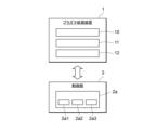
- FIG. 1 is a diagram for explaining a configuration example of a plasma processing system.
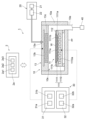
- FIG. 2 is a diagram for explaining a configuration example of a capacitively coupled plasma processing apparatus.
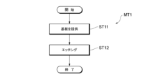
- 3 is a flowchart illustrating method MT1. It is a figure which shows an example of the cross-sectional structure of the board
- a substrate including a first film and a second film on the first film, the first film including silicon and the second film having at least one opening. and a step of etching the first film by generating plasma from a processing gas, the processing gas containing hydrogen fluoride gas, a first halogen-containing gas, and a first phosphorus-containing gas;
- An etching method is provided that includes a step in which the halogen-containing gas contains at least a halogen other than carbon and fluorine.
- the first halogen-containing gas is C s H t Br u Cl v F w , where s is an integer greater than or equal to 1 and less than or equal to 7, and the sum of u and v is an integer greater than or equal to 1. , t, u, v, and w are each an integer of 0 to 16).
- the first halogen-containing gas includes bromine as a halogen other than fluorine.
- the first halogen-containing gas includes chlorine as a halogen other than fluorine.
- the first halogen-containing gas further includes fluorine.
- the first halogen-containing gas includes at least one selected from the group consisting of CHCl 3 gas, CH 2 Cl 2 gas, and CF 2 Br 2 Cl 2 gas.
- the phosphorus-containing gas includes a halogenated phosphorus gas.
- the phosphorus-containing gas comprises an oxyhalogenated phosphorus gas.
- the oxyhalogenated ring gas includes at least one selected from the group consisting of POCl 3 gas, POCl 2 F gas, POClF 2 gas, and POF 3 gas.
- the phosphorus-containing gas includes an oxyhalogenated phosphorus gas and a halogenated phosphorus gas.
- the ratio of the partial pressure of the halogenated phosphorus gas to the partial pressure of the oxyhalogenated phosphorus gas is 0.1 or more and 3.0 or less.
- the ratio of the flow rates of the phosphorus-containing gas and the first halogen-containing gas to the total flow rate of the process gas is 20% by volume or less.
- the processing gas further includes a second halogen-containing gas different from the first halogen-containing gas.
- the second halogen-containing gas is carbon-free.
- the second halogen-containing gas includes a different type of halogen than the halogen contained in the first halogen-containing gas.
- the first film includes at least one selected from the group consisting of a silicon oxide film, a silicon nitride film, and a polysilicon film.
- the second film is a film containing at least one of carbon and metal.
- a substrate including a first film and a second film on the first film, the first film including silicon and the second film having at least one opening. and a step of etching the first film by generating plasma from a processing gas, the processing gas being one or more gases containing fluorine and hydrogen and capable of producing hydrogen fluoride in the plasma. , a first halogen-containing gas, and a phosphorus-containing gas, the first halogen-containing gas containing at least a halogen other than carbon and fluorine, and the phosphorus-containing gas containing phosphorus and a halogen.
- An etching method is provided that includes.
- the processing gas further includes a third halogen-containing gas, and the third halogen-containing gas is free of carbon and phosphorus.
- the controller includes a chamber and a controller, the controller providing a substrate in the chamber that includes a first film and a second film on the first film;
- the first film includes silicon
- the second film includes at least one opening
- the first film is etched by generating plasma from a processing gas
- the processing gas includes hydrogen fluoride gas, hydrogen fluoride gas, and at least one opening.
- a plasma processing apparatus is provided that is configured to perform control including a first halogen-containing gas and a phosphorus-containing gas, the first halogen-containing gas containing at least a halogen other than carbon and fluorine.
- FIG. 1 is a diagram for explaining a configuration example of a plasma processing system.
- a plasma processing system includes a plasma processing apparatus 1 and a controller 2.
- the plasma processing system is an example of a substrate processing system
- the plasma processing apparatus 1 is an example of a substrate processing apparatus.
- the plasma processing apparatus 1 includes a plasma processing chamber 10, a substrate support section 11, and a plasma generation section 12.
- the plasma processing chamber 10 has a plasma processing space.
- the plasma processing chamber 10 also includes at least one gas supply port for supplying at least one processing gas to the plasma processing space, and at least one gas exhaust port for discharging gas from the plasma processing space.
- the gas supply port is connected to a gas supply section 20, which will be described later, and the gas discharge port is connected to an exhaust system 40, which will be described later.
- the substrate support section 11 is disposed within the plasma processing space and has a substrate support surface for supporting a substrate.
- the plasma generation unit 12 is configured to generate plasma from at least one processing gas supplied into the plasma processing space.
- the plasmas formed in the plasma processing space are capacitively coupled plasma (CCP), inductively coupled plasma (ICP), and ECR plasma (Electron-Cyclotron-resonance plasma).
- CCP capacitively coupled plasma
- ICP inductively coupled plasma
- ECR plasma Electro-Cyclotron-resonance plasma
- HWP Helicon wave excited plasma
- SWP surface wave plasma
- various types of plasma generation sections may be used, including an AC (Alternating Current) plasma generation section and a DC (Direct Current) plasma generation section.
- the AC signal (AC power) used in the AC plasma generator has a frequency in the range of 100 kHz to 10 GHz. Therefore, the AC signal includes an RF (Radio Frequency) signal and a microwave signal.
- the RF signal has a frequency within the range of 100kHz to 150MHz.
- the control unit 2 processes computer-executable instructions that cause the plasma processing apparatus 1 to perform various steps described in this disclosure.
- the control unit 2 may be configured to control each element of the plasma processing apparatus 1 to perform the various steps described herein. In one embodiment, part or all of the control unit 2 may be included in the plasma processing apparatus 1.
- the control unit 2 may include a processing unit 2a1, a storage unit 2a2, and a communication interface 2a3.
- the control unit 2 is realized by, for example, a computer 2a.
- the processing unit two a1 may be configured to read a program from the storage unit two a2 and perform various control operations by executing the read program. This program may be stored in the storage unit 2a2 in advance, or may be acquired via a medium when necessary.
- the acquired program is stored in the storage unit 2a2, and is read out from the storage unit 2a2 and executed by the processing unit 2a1.
- the medium may be various storage media readable by the computer 2a, or may be a communication line connected to the communication interface 2a3.
- the processing unit 2a1 may be a CPU (Central Processing Unit).
- the storage unit 2a2 may include a RAM (Random Access Memory), a ROM (Read Only Memory), an HDD (Hard Disk Drive), an SSD (Solid State Drive), or a combination thereof. Good.
- the communication interface 2a3 may communicate with the plasma processing apparatus 1 via a communication line such as a LAN (Local Area Network).
- FIG. 2 is a diagram for explaining a configuration example of a capacitively coupled plasma processing apparatus.
- the capacitively coupled plasma processing apparatus 1 includes a plasma processing chamber 10, a gas supply section 20, a power supply 30, and an exhaust system 40. Further, the plasma processing apparatus 1 includes a substrate support section 11 and a gas introduction section. The gas inlet is configured to introduce at least one processing gas into the plasma processing chamber 10 .
- the gas introduction section includes a shower head 13.
- Substrate support 11 is arranged within plasma processing chamber 10 .
- the shower head 13 is arranged above the substrate support section 11 . In one embodiment, showerhead 13 forms at least a portion of the ceiling of plasma processing chamber 10 .
- the plasma processing chamber 10 has a plasma processing space 10s defined by a shower head 13, a side wall 10a of the plasma processing chamber 10, and a substrate support 11. Plasma processing chamber 10 is grounded.
- the shower head 13 and the substrate support section 11 are electrically insulated from the casing of the plasma processing chamber 10.
- the substrate support section 11 includes a main body section 111 and a ring assembly 112.
- the main body portion 111 has a central region 111a for supporting the substrate W and an annular region 111b for supporting the ring assembly 112.
- a wafer is an example of a substrate W.
- the annular region 111b of the main body 111 surrounds the central region 111a of the main body 111 in plan view.
- the substrate W is placed on the central region 111a of the main body 111, and the ring assembly 112 is placed on the annular region 111b of the main body 111 so as to surround the substrate W on the central region 111a of the main body 111. Therefore, the central region 111a is also called a substrate support surface for supporting the substrate W, and the annular region 111b is also called a ring support surface for supporting the ring assembly 112.
- the main body 111 includes a base 1110 and an electrostatic chuck 1111.
- Base 1110 includes a conductive member.
- the conductive member of the base 1110 can function as a bottom electrode.
- Electrostatic chuck 1111 is placed on base 1110.
- Electrostatic chuck 1111 includes a ceramic member 1111a and an electrostatic electrode 1111b disposed within ceramic member 1111a.
- Ceramic member 1111a has a central region 111a. In one embodiment, ceramic member 1111a also has an annular region 111b. Note that another member surrounding the electrostatic chuck 1111, such as an annular electrostatic chuck or an annular insulating member, may have the annular region 111b.
- ring assembly 112 may be placed on the annular electrostatic chuck or the annular insulation member, or may be placed on both the electrostatic chuck 1111 and the annular insulation member.
- at least one RF/DC electrode coupled to an RF power source 31 and/or a DC power source 32, which will be described later, may be disposed within the ceramic member 1111a.
- at least one RF/DC electrode functions as a bottom electrode.
- An RF/DC electrode is also referred to as a bias electrode if a bias RF signal and/or a DC signal, as described below, is supplied to at least one RF/DC electrode.
- the conductive member of the base 1110 and at least one RF/DC electrode may function as a plurality of lower electrodes.
- the electrostatic electrode 1111b may function as a lower electrode. Therefore, the substrate support 11 includes at least one lower electrode.
- Ring assembly 112 includes one or more annular members.
- the one or more annular members include one or more edge rings and at least one cover ring.
- the edge ring is made of a conductive or insulating material
- the cover ring is made of an insulating material.
- the substrate support unit 11 may include a temperature control module configured to adjust at least one of the electrostatic chuck 1111, the ring assembly 112, and the substrate to a target temperature.
- the temperature control module may include a heater, a heat transfer medium, a flow path 1110a, or a combination thereof.
- a heat transfer fluid such as brine or gas flows through the flow path 1110a.
- a channel 1110a is formed within the base 1110 and one or more heaters are disposed within the ceramic member 1111a of the electrostatic chuck 1111.
- the substrate support section 11 may include a heat transfer gas supply section configured to supply heat transfer gas to the gap between the back surface of the substrate W and the central region 111a.
- the shower head 13 is configured to introduce at least one processing gas from the gas supply section 20 into the plasma processing space 10s.
- the shower head 13 has at least one gas supply port 13a, at least one gas diffusion chamber 13b, and a plurality of gas introduction ports 13c.
- the processing gas supplied to the gas supply port 13a passes through the gas diffusion chamber 13b and is introduced into the plasma processing space 10s from the plurality of gas introduction ports 13c.
- the showerhead 13 also includes at least one upper electrode.
- the gas introduction section may include one or more side gas injectors (SGI) attached to one or more openings formed in the side wall 10a.
- SGI side gas injectors
- the gas supply section 20 may include at least one gas source 21 and at least one flow rate controller 22.
- the gas supply 20 is configured to supply at least one process gas from a respective gas source 21 to the showerhead 13 via a respective flow controller 22 .
- Each flow controller 22 may include, for example, a mass flow controller or a pressure-controlled flow controller.
- gas supply 20 may include at least one flow modulation device that modulates or pulses the flow rate of at least one process gas.
- Power supply 30 includes an RF power supply 31 coupled to plasma processing chamber 10 via at least one impedance matching circuit.
- RF power source 31 is configured to supply at least one RF signal (RF power) to at least one bottom electrode and/or at least one top electrode.
- RF power supply 31 can function as at least a part of the plasma generation section 12. Further, by supplying a bias RF signal to at least one lower electrode, a bias potential is generated in the substrate W, and ion components in the formed plasma can be drawn into the substrate W.
- the RF power supply 31 includes a first RF generation section 31a and a second RF generation section 31b.
- the first RF generation section 31a is coupled to at least one lower electrode and/or at least one upper electrode via at least one impedance matching circuit, and generates a source RF signal (source RF power) for plasma generation. It is configured as follows.
- the source RF signal has a frequency within the range of 10 MHz to 150 MHz.
- the first RF generator 31a may be configured to generate multiple source RF signals having different frequencies. The generated one or more source RF signals are provided to at least one bottom electrode and/or at least one top electrode.
- the second RF generating section 31b is coupled to at least one lower electrode via at least one impedance matching circuit, and is configured to generate a bias RF signal (bias RF power).
- the frequency of the bias RF signal may be the same or different than the frequency of the source RF signal.
- the bias RF signal has a lower frequency than the frequency of the source RF signal.
- the bias RF signal has a frequency within the range of 100kHz to 60MHz.
- the second RF generator 31b may be configured to generate multiple bias RF signals having different frequencies.
- the generated one or more bias RF signals are provided to at least one bottom electrode. Also, in various embodiments, at least one of the source RF signal and the bias RF signal may be pulsed.
- Power source 30 may also include a DC power source 32 coupled to plasma processing chamber 10 .
- the DC power supply 32 includes a first DC generation section 32a and a second DC generation section 32b.
- the first DC generator 32a is connected to at least one lower electrode and configured to generate a first DC signal.
- the generated first DC signal is applied to at least one bottom electrode.
- the second DC generator 32b is connected to the at least one upper electrode and configured to generate a second DC signal.
- the generated second DC signal is applied to the at least one top electrode.
- the first and second DC signals may be pulsed.
- a sequence of voltage pulses is applied to at least one lower electrode and/or at least one upper electrode.
- the voltage pulse may have a pulse waveform that is rectangular, trapezoidal, triangular, or a combination thereof.
- a waveform generator for generating a sequence of voltage pulses from a DC signal is connected between the first DC generator 32a and the at least one bottom electrode. Therefore, the first DC generation section 32a and the waveform generation section constitute a voltage pulse generation section.
- the voltage pulse generation section is connected to at least one upper electrode.
- the voltage pulse may have positive polarity or negative polarity.
- the sequence of voltage pulses may include one or more positive voltage pulses and one or more negative voltage pulses within one period.
- the first and second DC generation units 32a and 32b may be provided in addition to the RF power source 31, or the first DC generation unit 32a may be provided in place of the second RF generation unit 31b. good.
- the exhaust system 40 may be connected to a gas exhaust port 10e provided at the bottom of the plasma processing chamber 10, for example.
- Evacuation system 40 may include a pressure regulating valve and a vacuum pump. The pressure within the plasma processing space 10s is adjusted by the pressure regulating valve.
- the vacuum pump may include a turbomolecular pump, a dry pump, or a combination thereof.
- FIG. 3 is a flowchart illustrating an example of a plasma processing method (hereinafter also referred to as "method MT1") according to one exemplary embodiment.
- method MT1 includes a step ST11 of providing a substrate and a step ST12 of etching.
- the processing in each step may be performed in the plasma processing apparatus 1 shown in FIGS. 1 and 2.
- the control section 2 controls each section of the plasma processing apparatus 1 shown in FIG. 2 to execute the method MT1.
- step ST11 the substrate W is provided to the plasma processing chamber 10 (hereinafter also referred to as "chamber 10").
- the substrate W is carried into the chamber 10 by a transfer arm, placed on the substrate support 11 by a lifter, and held by suction on the substrate support 11 as shown in FIG.
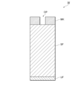
- FIG. 4 is a diagram showing an example of the cross-sectional structure of the substrate W provided in step ST11.
- the substrate W has a silicon-containing film SF and a mask MK placed on the silicon-containing film SF.
- the silicon-containing film SF may be formed on the base film UF.
- the substrate W may be used for manufacturing semiconductor devices.
- Semiconductor devices include, for example, memory devices such as DRAMs and 3D-NAND flash memories, and logic devices.
- the base film UF is a silicon wafer or an organic film, a dielectric film, a metal film, a semiconductor film, etc. formed on a silicon wafer.
- the base film UF may be configured by laminating a plurality of films.
- the silicon-containing film SF is a film to be etched by method MT1.
- the silicon-containing film SF is an example of the first film.
- the silicon-containing film SF may be a silicon oxide film, a silicon nitride film, a silicon carbonitride film, a polycrystalline silicon film, a carbon-containing silicon film.
- the silicon-containing film SF may be configured by stacking two or more films of one or more types.
- the silicon-containing film SF may be configured by alternately stacking silicon oxide films and silicon nitride films.
- the silicon-containing film SF may be configured by alternately stacking silicon oxide films and polycrystalline silicon films.
- the silicon-containing film SF may be a laminated film including a silicon nitride film, a silicon oxide film, and a polycrystalline silicon film.
- the silicon-containing film SF may be configured by stacking a silicon oxide film and a silicon carbonitride film.
- the silicon-containing film SF may be a laminated film including a silicon oxide film, a silicon nitride film, and a silicon carbonitride film.
- the silicon-containing film SF may be doped with elements such as phosphorous, boron or nitrogen.
- the mask MK is formed on the silicon-containing film SF.
- Mask MK is an example of the second film.
- Mask MK has at least one opening OP.
- the opening OP is a space above the silicon-containing film SF and is surrounded by the sidewall of the mask MK. That is, the upper surface of the silicon-containing film SF has a region covered by the mask MK and a region exposed at the bottom of the opening OP.
- the opening OP may be a hole or a slit.
- the mask MK may be a carbon-containing film.
- the carbon-containing film includes, for example, at least one selected from the group consisting of a spin-on carbon (SOC) film, tungsten carbide, an amorphous carbon (ACL) film, a boron carbide film, and a photoresist film.
- SOC spin-on carbon
- ACL amorphous carbon
- the ACL film may be doped with elements such as boron, arsenic, tungsten, xenon, etc.
- the mask MK may be a metal-containing film.
- the metal-containing film contains at least one metal selected from the group consisting of tungsten, molybdenum, ruthenium, and titanium.
- the metal-containing film may include, for example, a carbide or silicide of tungsten, molybdenum or titanium.
- the metal-containing film may be, for example, a tungsten-containing film.
- the metal-containing film may further include tungsten and at least one member selected from the group consisting of silicon, carbon, and nitrogen.
- the metal-containing film includes at least one selected from the group consisting of WC (tungsten carbide), WSi (tungsten silicide), WSiN, and WSiC.
- Mask MK may be a single layer mask consisting of one layer, or may be a multilayer mask consisting of two or more layers.
- the base film UF, silicon-containing film SF, and mask MK may each be formed by any method.
- the base film UF, silicon-containing film SF, and mask MK may be formed by a CVD method, an ALD method, a PVD method, a spin coating method, or the like, respectively.
- Mask MK may be formed by lithography, for example.
- the opening OP of the mask MK may be formed by etching the mask MK.
- the base film UF, silicon-containing film SF, and mask MK may each be a flat film, or may be a film with unevenness.
- the substrate W may further include another film under the base film UF. In this case, a recessed portion having a shape corresponding to the opening OP may be formed in the silicon-containing film SF and the base film UF, and may be used as a mask for etching the other film.
- the process of forming the base film UF, silicon-containing film SF, and mask MK of the substrate W may be performed in the chamber 10 as part of step ST11.
- the etching in step ST11 and the etching in step ST12 which will be described later, may be performed continuously in the chamber 10.
- the substrate W may be provided into the chamber 10 after all or part of the substrate W has been formed in an apparatus or chamber external to the plasma processing apparatus 1 .
- the substrate support 11 is controlled to a set temperature by the temperature control module.
- the set temperature is, for example, room temperature (for example, 25°C) or lower, 0°C or lower, -10°C or lower, -20°C or lower, -30°C or lower, -40°C or lower, -50°C or lower, -60°C or lower, or -70°C or lower.
- the temperature may be below °C.
- the set temperature may be, for example, -100°C or higher or -90°C or higher.
- controlling the temperature of the substrate support 11 to a set temperature means that the temperature of the heat transfer fluid flowing through the flow path 1110a or the heater temperature is set to the set temperature, or a temperature different from the set temperature. including making it.
- the timing at which the heat transfer fluid starts flowing into the flow path 1110a may be before or after the substrate W is placed on the substrate support 11, or may be at the same time.
- the temperature of the substrate support section 11 may be controlled to a set temperature before step ST11. That is, the substrate W may be provided to the substrate support 11 after the temperature of the substrate support 11 is controlled to the set temperature.
- the substrate W may be controlled to a set temperature.
- Controlling the temperature of the substrate W to a set temperature means setting the temperature of the heat transfer fluid flowing through the substrate support 11 and the flow path 1110a and/or the heater temperature to the set temperature, or setting the temperature to a temperature different from the set temperature. Including.
- step ST12 the silicon-containing film SF is etched using plasma generated from the processing gas.
- a processing gas is supplied from the gas supply section 20 into the plasma processing space 10s.
- the processing gas includes hydrogen fluoride (HF) gas, phosphorus-containing gas, and first halogen-containing gas.
- the HF gas may have the highest flow rate (partial pressure) of the process gases other than the inert gases.
- the flow rate of the HF gas is 50% by volume or more, 60% by volume or more, It may be 70 volume% or more, 80 volume% or more, 90 volume% or more, or 95 volume% or more.
- the flow rate of the HF gas may be less than 100 volume %, 99.5 volume % or less, 98 volume % or less, or 96 volume % or less with respect to the total flow rate of the processing gas.
- the flow rate of the HF gas is greater than or equal to 70% by volume and less than or equal to 96% by volume based on the total flow rate of the processing gas.
- the process gas may include a gas capable of generating hydrogen fluoride species (HF species) in the plasma in place of some or all of the HF gas.
- HF species includes at least one of hydrogen fluoride gas, radicals, and ions.
- the gas capable of producing HF species may be, for example, a hydrofluorocarbon gas.
- the hydrofluorocarbon gas may have 2 or more carbon atoms, 3 or more carbon atoms, or 4 or more carbon atoms.
- Hydrofluorocarbon gases include , for example, CH2F2 gas , C3H2F4 gas , C3H2F6 gas , C3H3F5 gas , C4H2F6 gas , and C4H5 .
- the gas is at least one selected from the group consisting of F5 gas, C4H2F8 gas, C5H2F6 gas , C5H2F10 gas, and C5H3F7 gas .
- the hydrofluorocarbon gas is at least one selected from the group consisting of CH 2 F 2 gas, C 3 H 2 F 4 gas, C 3 H 2 F 6 gas, and C 4 H 2 F 6 gas.
- the gas capable of producing HF species may be, for example, a mixed gas containing a hydrogen source and a fluorine source.
- the hydrogen source is, for example, at least one type selected from the group consisting of H 2 gas, NH 3 gas, H 2 O gas, H 2 O 2 gas, and hydrocarbon gas (CH 4 gas, C 3 H 6 gas, etc.). good.
- the fluorine source may be a carbon-free fluorine-containing gas, such as NF3 gas, SF6 gas, WF6 gas or XeF2 gas.
- the fluorine source may also be a fluorine-containing gas containing carbon, such as fluorocarbon gas and hydrofluorocarbon gas.
- Fluorocarbon gases include , in one example , CF4 gas, C2F2 gas, C2F4 gas, C3F6 gas , C3F8 gas , C4F6 gas , C4F8 gas , and C5F . At least one gas selected from the group consisting of 8 gases may be used.
- the hydrofluorocarbon gas include CHF 3 gas, CH 2 F 2 gas, CH 3 F gas, C 2 HF 5 gas, and hydrofluorocarbon gas containing three or more C (C 3 H 2 F 4 gas, C 3 H 2 F 6 gas, C 4 H 2 F 6 gas, etc.).
- the phosphorus-containing gas may include an oxyhalogenated phosphorus gas.
- the oxyhalogenated phosphorous gas may be at least one selected from the group consisting of POCl 3 gas, POCl 2 F gas, POClF 2 gas, and POF 3 gas.
- the oxyhalogenated phosphorus gas may be POCl 3 gas or POF 3 gas.
- the phosphorus-containing gas may include halogenated phosphorus gases in addition to the oxyhalogenated phosphorus gases described above.
- the halogenated phosphorous gas is a gas that includes phosphorus, fluorine and/or chlorine, and is oxygen-free.
- the halogenated phosphorus gas may be at least one selected from the group consisting of PF3 gas, PF5 gas, PCl3 gas, PCl5 gas, PClF2 gas, PCl2F gas, and PCl2F3 .
- the halogenated phosphorous gas may be PF3 gas, PF5 gas, or PCl3 gas.
- the ratio of the flow rate (partial pressure) of the halogenated phosphorus gas to the flow rate (partial pressure) of the oxyhalogenated phosphorus gas is 0.1. It may be 0.2 or more or 0.3 or more. Further, the ratio of the flow rate (partial pressure) of the halogenated phosphorus gas to the flow rate (partial pressure) of the oxyhalogenated phosphorus gas may be 3.0 or less, 2.0 or less, or 1.0 or less.
- the ratio of the flow rate (partial pressure) of the halogenated phosphorus gas to the flow rate (partial pressure) of the oxyhalogenated phosphorus gas is 0.2 or more and 3.0 or less.
- the first halogen-containing gas is a gas that includes at least a halogen other than carbon and fluorine.
- the halogen other than fluorine may be at least one selected from the group consisting of bromine (Br), chlorine (Cl), and iodine (I).
- the halogen other than fluorine may include a different type of halogen from the halogen contained in the phosphorus-containing gas.
- the first halogen-containing gas is C s H t Br u Cl v F w (s is an integer greater than or equal to 1 and less than or equal to 7, the sum of u and v is an integer greater than or equal to 1, and t , u, v, and w are each an integer of 0 to 16).
- the first halogen-containing gas is at least one gas selected from the group consisting of CH 3 Br gas, CH 2 BrF gas, CBr 2 F 2 gas, CBr 2 ClF gas, and CHBrCl 2 gas. good.
- the first halogen-containing gas is CCl 4 gas, CH 2 Cl 2 gas, CHCl 3 gas, CF 2 Cl 2 gas, CH 2 ClF gas, CHCl 2 F gas, C 2 F 5 Br gas, CF 3
- the gas may be at least one selected from the group consisting of I gas, C 2 F 5 I gas, and C 3 F 7 I gas.
- the ratio of the flow rate (partial pressure) of the first halogen-containing gas to the flow rate (partial pressure) of the phosphorus-containing gas is determined by the film type of the silicon-containing film SF, the flow rate (partial pressure) of the HF gas, It may be set as appropriate depending on the type and atomic ratio of the halogen contained in the contained gas and the first halogen-containing gas, the desired shape, etc.
- the ratio of the flow rate (partial pressure) of the first halogen-containing gas to the flow rate (partial pressure) of the phosphorus-containing gas may be greater than or equal to 0.1, greater than or equal to 0.2, or greater than or equal to 0.3.
- the ratio of the flow rate (partial pressure) of the first halogen-containing gas to the flow rate (partial pressure) of the phosphorus-containing gas may be 1.5 or less, 1.2 or less, or 1.0 or less. In one example, the ratio of the flow rate (partial pressure) of the halogen-containing gas to the flow rate (partial pressure) of the phosphorus-containing gas is 0.1 or more and 1.5 or less.
- the total flow rate of the phosphorus-containing gas and the first halogen-containing gas relative to the total flow rate of the process gas (or the total flow rate of all gases except the inert gas, if the process gas includes an inert gas).
- the proportion may be controlled to 20% by volume or less, 15% by volume or less or 10% by volume or less.
- the processing gas may include gases other than HF gas, phosphorus-containing gas, and the first halogen-containing gas.
- the processing gas may further include at least one gas selected from the group consisting of a second halogen-containing gas, a carbon-containing gas, a tungsten-containing gas, and an oxygen-containing gas.
- the second halogen-containing gas is different from the first halogen-containing gas.
- the second halogen-containing gas contains a halogen other than the halogen contained in the first halogen-containing gas.
- the first halogen-containing gas contains bromine (Br) and does not contain chlorine (Cl)
- the second halogen-containing gas may contain at least chlorine (Cl).
- the first halogen-containing gas contains chlorine (Cl) and does not contain bromine (Br)
- the second halogen-containing gas may contain at least bromine (Br).
- at least one of the first halogen-containing gas and the second halogen-containing gas may include chlorine (Cl).
- at least one of the first halogen-containing gas and the second halogen-containing gas may include bromine (Br).
- the second halogen-containing gas may contain a halogen other than fluorine.
- the second halogen-containing gas may be a chlorine-containing gas, a bromine-containing gas, and/or an iodine-containing gas.
- the chlorine-containing gas is, in one example, from Cl2 , SiCl2 , SiCl4 , CCl4 , SiH2Cl2 , Si2Cl6 , CHCl3 , SO2Cl2 , BCl3 , PCl3 , PCl5 , and POCl3.
- the bromine-containing gas may be, in one example, at least one gas selected from the group consisting of Br2 , HBr, CBr2F2 , C2F5Br , PBr3 , PBr5 , POBr3, and BBr3 .
- the iodine-containing gas is at least one gas selected from the group consisting of HI , CF3I , C2F5I , C3F7I , IF5 , IF7 , I2 , and PI3 . good.
- the second halogen-containing gas may be at least one selected from the group consisting of Cl 2 gas, Br 2 gas, and HBr gas.
- the second halogen-containing gas is Cl2 gas or HBr gas.
- the carbon-containing gas may be, for example, either or both of a fluorocarbon gas and a hydrofluorocarbon gas.
- the fluorocarbon gases include CF4 gas, C2F2 gas, C2F4 gas, C3F6 gas , C3F8 gas , C4F6 gas , C4F8 gas , and C5F .
- At least one gas selected from the group consisting of 8 gases may be used.
- the hydrofluorocarbon gas is CHF3 gas, CH2F2 gas , CH3F gas , C2HF5 gas , C2H2F4 gas , C2H3F3 gas , C2H4F 2 gas, C 3 HF 7 gas, C 3 H 2 F 2 gas, C 3 H 2 F 4 gas, C 3 H 2 F 6 gas, C 3 H 3 F 5 gas, C 4 H 2 F 6 gas, C At least one type selected from the group consisting of 4 H 5 F 5 gas, C 4 H 2 F 8 gas, C 5 H 2 F 6 gas, C 5 H 2 F 10 gas, and C 5 H 3 F 7 gas may be used.
- the carbon-containing gas may be a linear gas having an unsaturated bond.
- linear carbon-containing gases having unsaturated bonds examples include C 3 F 6 (hexafluoropropene) gas, C 4 F 8 (octafluoro-1-butene, octafluoro-2-butene) gas, C 3 H 2 F 4 (1,3,3,3-tetrafluoropropene) gas, C 4 H 2 F 6 (trans-1, 1, 1, 4, 4, 4-hexafluoro-2-butene) gas , C 4 F 8 O (pentafluoroethyl trifluorovinyl ether) gas, CF 3 COF gas (1,2,2,2-tetrafluoroethane-1-one), CHF 2 COF (difluoroacetic acid fluoride) gas and COF 2 (carbonyl fluoride) gas may be used.
- C 3 F 6 hexafluoropropene
- C 4 F 8 octafluoro-1-butene, octafluoro-2-butene
- the tungsten-containing gas may be, for example, a gas containing tungsten and halogen.
- the tungsten-containing gas includes tungsten difluoride (WF 2 ) gas, tungsten tetrafluoride (WF 4 ) gas, tungsten pentafluoride (WF 5 ) gas, and tungsten hexafluoride (WF 6 ) gas.
- Tungsten and fluorine-containing gases such as tungsten dichloride (WCl 2 ) gas, tungsten tetrachloride (WCl 4 ) gas, tungsten pentachloride (WCl 5 ) gas, tungsten hexachloride (WCl 6 ) gas, etc.
- It may be a gas containing chlorine.
- at least one of WF 6 gas and WCl 6 gas may be used.
- the flow rate of the tungsten-containing gas may be 5% by volume or less of the total flow rate of the processing gas.
- the processing gas may include at least one of a titanium-containing gas, a ruthenium-containing gas, and/or a molybdenum-containing gas instead of or in addition to the tungsten-containing gas.
- the oxygen-containing gas may be, for example, at least one gas selected from the group consisting of O 2 , CO, CO 2 , H 2 O, and H 2 O 2 .
- the oxygen- containing gas may be an oxygen-containing gas other than H2O , such as at least one gas selected from the group consisting of O2 , CO, CO2, and H2O2 .
- the processing gas may further include an inert gas.
- the inert gas may be a noble gas such as Ar gas, He gas, Kr gas, or nitrogen gas.
- the gas contained in the process gas and its flow rate (partial pressure) may or may not be changed.
- the silicon-containing film SF is composed of a laminated film consisting of different types of silicon-containing films
- the composition of the processing gas and the flow rate (partial pressure) of each gas will change as the etching progresses (i.e., the thickness of the film to be etched). (depending on the type) may be changed.
- the temperature of the substrate support section 11 may be maintained at the set temperature adjusted in step ST11, or may be changed.
- step ST12 after the above-described processing gas is supplied into the plasma processing space 10s, plasma is generated from the processing gas. As a result, the substrate W is etched.
- plasma generation may be performed as follows. First, a source RF signal is supplied to the lower electrode of the substrate support 11 and/or at least one upper electrode of the showerhead 13 . As a result, a high frequency electric field is generated between the shower head 13 and the substrate support section 11, and plasma is generated from the processing gas in the chamber 10. Further, a bias signal is supplied to the lower electrode of the substrate support section 11. As a result, active species in the plasma are attracted to the substrate W, and the silicon-containing film SF is etched.
- the bias signal may be a bias RF signal supplied from the second RF generator 31b. Further, the bias signal may be a bias DC signal supplied from the DC generation section 32a.
- the source RF signal and the bias signal may both be continuous waves or pulsed waves, or one may be continuous wave and the other pulsed wave. When both the source RF signal and the bias signal are pulse waves, the periods of both pulse waves may or may not be synchronized.
- the duty ratio of the source RF signal and/or bias signal pulse wave may be set as appropriate, for example, from 1 to 80%, or from 5 to 50%. Note that the duty ratio is the ratio of the period in which the power or voltage level is high to the period of the pulse wave.
- the pulse wave may have a waveform of a rectangle, a trapezoid, a triangle, or a combination thereof.
- the polarity of the bias DC signal may be negative or positive as long as the potential of the substrate W is set so as to provide a potential difference between the plasma and the substrate and draw in ions.
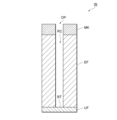
- FIG. 5 is a diagram showing an example of the cross-sectional structure of the substrate W at the end of step ST12.
- the portion of the silicon-containing film SF exposed at the opening OP is etched in the depth direction (from top to bottom in FIG. 5), and a recess RC is formed.
- FIG. 5 is an example in which the bottom part BT of the recess RC reaches the base film UF and the base film UF is exposed due to the etching in step ST12.
- the aspect ratio of the recessed portion RC in this state may be, for example, 20 or more, 30 or more, 40 or more, 50 or more, or 100 or more.
- the processing gas includes HF gas, phosphorus-containing gas, and first halogen-containing gas.
- the HF gas generates HF species in the plasma and functions as an etchant for the silicon-containing film SF.
- the phosphorus-containing gas promotes the reaction between the HF species and the silicon-containing film SF.
- the phosphorus-containing gas is an oxyhalogenated phosphorus gas and/or a halogenated phosphorus gas
- the phosphorus-containing gas promotes the reaction between the HF species and the silicon-containing film SF, and also improves the etching shape and the opening OP. It can contribute to suppressing occlusion (clogging).
- the first halogen-containing gas contributes to improving the etching shape and protecting the mask MK.
- the improvement of the etched shape may be an improvement in roundness, suppression of bending, and/or suppression of bowing.
- the first halogen-containing gas or phosphorus-containing gas is a gas that has multiple functions in etching as described above. Since these gases are composed of one molecule, the partial pressure in the processing gas can be kept lower than when two or more different gases are combined to obtain the same function. Thereby, the partial pressure of HF gas, which is an etchant, in the processing gas can be increased. Therefore, according to method MT1, it is possible to improve the etching shape, suppress clogging, or protect the mask while maintaining a high partial pressure of HF gas.
- a technique for improving etched features can be provided.
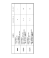
- FIG. 6 is a diagram for explaining an example and a reference example.
- Example 1 Using the plasma processing apparatus 1 shown in FIG. 2, the substrate W shown in FIG. 4 was etched according to the flow chart explained in FIG. First, in step ST11, the substrate W was provided on the substrate support section 11.
- the silicon-containing film SF of the substrate W was a multilayer laminated film consisting of a silicon oxide film and a silicon nitride film.
- Mask MK was an amorphous carbon film having hole-shaped openings OP.
- step ST12 the silicon-containing film SF was etched using plasma generated from the processing gas shown in the "Example 1" column of FIG.
- Example 2 is the same as Example 1 except that in step ST12, the processing gas shown in the "Example 2" column of FIG. 6 was used.
- etching rate is the etching rate of each example when the etching rate of the reference example is set to 1.
- Boeing indicates the CD of bowing that occurred in the silicon-containing film SF of each example, when the CD (critical dimension) of bowing that occurred in the silicon-containing film SF of the reference example is set to 1.
- both Example 1 and Example 2 achieved an etching rate comparable to that of the reference example.
- both Example 1 and Example 2 were able to suppress bowing to the same extent as the reference example.
- Embodiments of the present disclosure further include the following aspects.
- the first halogen-containing gas is C s H t Br u Cl v F w (s is an integer of 1 or more and 7 or less, the sum of u and v is an integer of 1 or more, and t, u, v and
- the first halogen-containing gas meets any one of appendices 1 to 5, including at least one selected from the group consisting of CHCl 3 gas, CH 2 Cl 2 gas, and CF 2 Br 2 Cl 2 gas. Etching method described.
- Appendix 12 The etching method according to any one of appendices 1 to 11, wherein the ratio of the flow rates of the phosphorus-containing gas and the first halogen-containing gas to the total flow rate of the processing gas is 20% by volume or less.
- Appendix 16 The etching method according to any one of appendices 1 to 15, wherein the first film includes at least one selected from the group consisting of a silicon oxide film, a silicon nitride film, and a polysilicon film.
- Appendix 17 The etching method according to any one of appendices 1 to 16, wherein the second film is a film containing at least one of carbon and metal.
- (Appendix 18) providing a substrate including a first film and a second film on the first film, the first film including silicon and the second film including at least one opening; , a step of etching the first film by generating plasma from a processing gas, the processing gas containing at least one type of gas containing fluorine and hydrogen and capable of producing hydrogen fluoride in the plasma; a halogen-containing gas, and a phosphorus-containing gas, the first halogen-containing gas containing at least a halogen other than carbon and fluorine, and the phosphorus-containing gas containing phosphorus and a halogen; Etching methods including.
- the control unit includes: A control for providing in the chamber a substrate including a first film and a second film on the first film, wherein the first film includes silicon and the second film has at least one opening. including, control, and Control for etching the first film by generating plasma from a processing gas, wherein the processing gas includes hydrogen fluoride gas, a first halogen-containing gas, and a phosphorus-containing gas, and the first halogen-containing gas comprises at least a halogen other than carbon and fluorine, and is configured to perform: Plasma processing equipment.
- SYMBOLS 1 Plasma processing apparatus, 2... Control part, 10... Plasma processing chamber, 10s... Plasma processing space, 11... Substrate support part, 13... shower head, 20... Gas supply part, 31a... First RF generation section, 31b... Second RF generation section, 32a... First DC generation section, SF... Silicon-containing film, MK... Mask, OP... Opening, RC... Concavity, UF ... Base film, W ... Substrate
Landscapes
- Chemical & Material Sciences (AREA)
- Engineering & Computer Science (AREA)
- Physics & Mathematics (AREA)
- Plasma & Fusion (AREA)
- Analytical Chemistry (AREA)
- Inorganic Chemistry (AREA)
- Materials Engineering (AREA)
- Organic Chemistry (AREA)
- Drying Of Semiconductors (AREA)
Priority Applications (5)
| Application Number | Priority Date | Filing Date | Title |
|---|---|---|---|
| KR1020257008613A KR20250056935A (ko) | 2022-08-26 | 2023-08-22 | 에칭 방법 및 플라즈마 처리 장치 |
| JP2024542826A JPWO2024043239A1 (cg-RX-API-DMAC7.html) | 2022-08-26 | 2023-08-22 | |
| CN202380059568.8A CN119698689A (zh) | 2022-08-26 | 2023-08-22 | 蚀刻方法及等离子体处理装置 |
| TW112132052A TW202425126A (zh) | 2022-08-26 | 2023-08-25 | 蝕刻方法及電漿處理裝置 |
| US19/062,449 US20250215320A1 (en) | 2022-08-26 | 2025-02-25 | Etching method and plasma processing apparatus |
Applications Claiming Priority (2)
| Application Number | Priority Date | Filing Date | Title |
|---|---|---|---|
| US202263373572P | 2022-08-26 | 2022-08-26 | |
| US63/373,572 | 2022-08-26 |
Related Child Applications (1)
| Application Number | Title | Priority Date | Filing Date |
|---|---|---|---|
| US19/062,449 Continuation US20250215320A1 (en) | 2022-08-26 | 2025-02-25 | Etching method and plasma processing apparatus |
Publications (1)
| Publication Number | Publication Date |
|---|---|
| WO2024043239A1 true WO2024043239A1 (ja) | 2024-02-29 |
Family
ID=90013394
Family Applications (1)
| Application Number | Title | Priority Date | Filing Date |
|---|---|---|---|
| PCT/JP2023/030184 Ceased WO2024043239A1 (ja) | 2022-08-26 | 2023-08-22 | エッチング方法及びプラズマ処理装置 |
Country Status (6)
| Country | Link |
|---|---|
| US (1) | US20250215320A1 (cg-RX-API-DMAC7.html) |
| JP (1) | JPWO2024043239A1 (cg-RX-API-DMAC7.html) |
| KR (1) | KR20250056935A (cg-RX-API-DMAC7.html) |
| CN (1) | CN119698689A (cg-RX-API-DMAC7.html) |
| TW (1) | TW202425126A (cg-RX-API-DMAC7.html) |
| WO (1) | WO2024043239A1 (cg-RX-API-DMAC7.html) |
Citations (2)
| Publication number | Priority date | Publication date | Assignee | Title |
|---|---|---|---|---|
| JP2020115538A (ja) * | 2018-06-04 | 2020-07-30 | 東京エレクトロン株式会社 | エッチング処理方法およびエッチング処理装置 |
| WO2021090798A1 (ja) * | 2019-11-08 | 2021-05-14 | 東京エレクトロン株式会社 | エッチング方法 |
Family Cites Families (1)
| Publication number | Priority date | Publication date | Assignee | Title |
|---|---|---|---|---|
| JP6423643B2 (ja) | 2014-08-08 | 2018-11-14 | 東京エレクトロン株式会社 | 多層膜をエッチングする方法 |
-
2023
- 2023-08-22 JP JP2024542826A patent/JPWO2024043239A1/ja active Pending
- 2023-08-22 CN CN202380059568.8A patent/CN119698689A/zh active Pending
- 2023-08-22 KR KR1020257008613A patent/KR20250056935A/ko active Pending
- 2023-08-22 WO PCT/JP2023/030184 patent/WO2024043239A1/ja not_active Ceased
- 2023-08-25 TW TW112132052A patent/TW202425126A/zh unknown
-
2025
- 2025-02-25 US US19/062,449 patent/US20250215320A1/en active Pending
Patent Citations (2)
| Publication number | Priority date | Publication date | Assignee | Title |
|---|---|---|---|---|
| JP2020115538A (ja) * | 2018-06-04 | 2020-07-30 | 東京エレクトロン株式会社 | エッチング処理方法およびエッチング処理装置 |
| WO2021090798A1 (ja) * | 2019-11-08 | 2021-05-14 | 東京エレクトロン株式会社 | エッチング方法 |
Also Published As
| Publication number | Publication date |
|---|---|
| TW202425126A (zh) | 2024-06-16 |
| JPWO2024043239A1 (cg-RX-API-DMAC7.html) | 2024-02-29 |
| US20250215320A1 (en) | 2025-07-03 |
| KR20250056935A (ko) | 2025-04-28 |
| CN119698689A (zh) | 2025-03-25 |
Similar Documents
| Publication | Publication Date | Title |
|---|---|---|
| KR102815322B1 (ko) | 에칭 방법 및 플라즈마 처리 시스템 | |
| US20220157610A1 (en) | Etching method | |
| JP7348672B2 (ja) | プラズマ処理方法及びプラズマ処理システム | |
| JP7529902B2 (ja) | エッチング方法及びプラズマ処理システム | |
| KR20230161883A (ko) | 에칭 방법 및 플라즈마 처리 시스템 | |
| WO2023238903A1 (ja) | エッチング方法およびプラズマ処理装置 | |
| WO2024043082A1 (ja) | エッチング方法及びプラズマ処理システム | |
| JP2023127546A (ja) | プラズマ処理方法及びプラズマ処理装置 | |
| JP2023143889A (ja) | プラズマ処理方法及びプラズマ処理システム | |
| TW202507839A (zh) | 蝕刻方法及蝕刻裝置 | |
| US20230282447A1 (en) | Plasma processing method and plasma processing apparatus | |
| US20250215320A1 (en) | Etching method and plasma processing apparatus | |
| JP7785422B2 (ja) | エッチング方法及びプラズマ処理装置 | |
| JP2023171269A (ja) | エッチング方法及びプラズマ処理システム | |
| WO2025150427A1 (ja) | エッチング方法及びプラズマ処理システム | |
| WO2025150267A1 (ja) | プラズマ処理装置及びプラズマ処理方法 | |
| JP2024176159A (ja) | プラズマ処理方法及びプラズマ処理装置 | |
| JP2023181081A (ja) | エッチング方法及びプラズマ処理システム | |
| WO2025234350A1 (ja) | エッチング方法及びプラズマ処理装置 | |
| JP2024150167A (ja) | プラズマ処理方法及びプラズマ処理装置 | |
| JP2023151985A (ja) | エッチング方法及びプラズマ処理システム | |
| WO2024219232A1 (ja) | エッチング方法及びプラズマ処理装置 | |
| CN116705601A (zh) | 等离子体处理方法和等离子体处理装置 |
Legal Events
| Date | Code | Title | Description |
|---|---|---|---|
| 121 | Ep: the epo has been informed by wipo that ep was designated in this application |
Ref document number: 23857348 Country of ref document: EP Kind code of ref document: A1 |
|
| WWE | Wipo information: entry into national phase |
Ref document number: 2024542826 Country of ref document: JP |
|
| WWE | Wipo information: entry into national phase |
Ref document number: 202380059568.8 Country of ref document: CN |
|
| ENP | Entry into the national phase |
Ref document number: 20257008613 Country of ref document: KR Kind code of ref document: A |
|
| WWE | Wipo information: entry into national phase |
Ref document number: 1020257008613 Country of ref document: KR |
|
| WWP | Wipo information: published in national office |
Ref document number: 202380059568.8 Country of ref document: CN |
|
| NENP | Non-entry into the national phase |
Ref country code: DE |
|
| WWE | Wipo information: entry into national phase |
Ref document number: 11202501267Q Country of ref document: SG |
|
| WWP | Wipo information: published in national office |
Ref document number: 11202501267Q Country of ref document: SG |
|
| WWP | Wipo information: published in national office |
Ref document number: 1020257008613 Country of ref document: KR |
|
| 122 | Ep: pct application non-entry in european phase |
Ref document number: 23857348 Country of ref document: EP Kind code of ref document: A1 |