WO2024038685A1 - 半導体装置、半導体モジュール及び電子機器 - Google Patents
半導体装置、半導体モジュール及び電子機器 Download PDFInfo
- Publication number
- WO2024038685A1 WO2024038685A1 PCT/JP2023/023897 JP2023023897W WO2024038685A1 WO 2024038685 A1 WO2024038685 A1 WO 2024038685A1 JP 2023023897 W JP2023023897 W JP 2023023897W WO 2024038685 A1 WO2024038685 A1 WO 2024038685A1
- Authority
- WO
- WIPO (PCT)
- Prior art keywords
- field effect
- gate
- effect transistor
- transistor
- semiconductor device
- Prior art date
- Legal status (The legal status is an assumption and is not a legal conclusion. Google has not performed a legal analysis and makes no representation as to the accuracy of the status listed.)
- Ceased
Links
Images









Classifications
-
- H—ELECTRICITY
- H10—SEMICONDUCTOR DEVICES; ELECTRIC SOLID-STATE DEVICES NOT OTHERWISE PROVIDED FOR
- H10D—INORGANIC ELECTRIC SEMICONDUCTOR DEVICES
- H10D89/00—Aspects of integrated devices not covered by groups H10D84/00 - H10D88/00
- H10D89/60—Integrated devices comprising arrangements for electrical or thermal protection, e.g. protection circuits against electrostatic discharge [ESD]
-
- H—ELECTRICITY
- H02—GENERATION; CONVERSION OR DISTRIBUTION OF ELECTRIC POWER
- H02H—EMERGENCY PROTECTIVE CIRCUIT ARRANGEMENTS
- H02H9/00—Emergency protective circuit arrangements for limiting excess current or voltage without disconnection
- H02H9/005—Emergency protective circuit arrangements for limiting excess current or voltage without disconnection avoiding undesired transient conditions
-
- H—ELECTRICITY
- H02—GENERATION; CONVERSION OR DISTRIBUTION OF ELECTRIC POWER
- H02H—EMERGENCY PROTECTIVE CIRCUIT ARRANGEMENTS
- H02H9/00—Emergency protective circuit arrangements for limiting excess current or voltage without disconnection
- H02H9/04—Emergency protective circuit arrangements for limiting excess current or voltage without disconnection responsive to excess voltage
-
- H—ELECTRICITY
- H10—SEMICONDUCTOR DEVICES; ELECTRIC SOLID-STATE DEVICES NOT OTHERWISE PROVIDED FOR
- H10D—INORGANIC ELECTRIC SEMICONDUCTOR DEVICES
- H10D30/00—Field-effect transistors [FET]
- H10D30/01—Manufacture or treatment
- H10D30/021—Manufacture or treatment of FETs having insulated gates [IGFET]
-
- H—ELECTRICITY
- H10—SEMICONDUCTOR DEVICES; ELECTRIC SOLID-STATE DEVICES NOT OTHERWISE PROVIDED FOR
- H10D—INORGANIC ELECTRIC SEMICONDUCTOR DEVICES
- H10D30/00—Field-effect transistors [FET]
- H10D30/01—Manufacture or treatment
- H10D30/051—Manufacture or treatment of FETs having PN junction gates
-
- H—ELECTRICITY
- H10—SEMICONDUCTOR DEVICES; ELECTRIC SOLID-STATE DEVICES NOT OTHERWISE PROVIDED FOR
- H10D—INORGANIC ELECTRIC SEMICONDUCTOR DEVICES
- H10D30/00—Field-effect transistors [FET]
- H10D30/40—FETs having zero-dimensional [0D], one-dimensional [1D] or two-dimensional [2D] charge carrier gas channels
- H10D30/47—FETs having zero-dimensional [0D], one-dimensional [1D] or two-dimensional [2D] charge carrier gas channels having two-dimensional [2D] charge carrier gas channels, e.g. nanoribbon FETs or high electron mobility transistors [HEMT]
- H10D30/471—High electron mobility transistors [HEMT] or high hole mobility transistors [HHMT]
-
- H—ELECTRICITY
- H10—SEMICONDUCTOR DEVICES; ELECTRIC SOLID-STATE DEVICES NOT OTHERWISE PROVIDED FOR
- H10D—INORGANIC ELECTRIC SEMICONDUCTOR DEVICES
- H10D30/00—Field-effect transistors [FET]
- H10D30/40—FETs having zero-dimensional [0D], one-dimensional [1D] or two-dimensional [2D] charge carrier gas channels
- H10D30/47—FETs having zero-dimensional [0D], one-dimensional [1D] or two-dimensional [2D] charge carrier gas channels having two-dimensional [2D] charge carrier gas channels, e.g. nanoribbon FETs or high electron mobility transistors [HEMT]
- H10D30/471—High electron mobility transistors [HEMT] or high hole mobility transistors [HHMT]
- H10D30/475—High electron mobility transistors [HEMT] or high hole mobility transistors [HHMT] having wider bandgap layer formed on top of lower bandgap active layer, e.g. undoped barrier HEMTs such as i-AlGaN/GaN HEMTs
-
- H—ELECTRICITY
- H10—SEMICONDUCTOR DEVICES; ELECTRIC SOLID-STATE DEVICES NOT OTHERWISE PROVIDED FOR
- H10D—INORGANIC ELECTRIC SEMICONDUCTOR DEVICES
- H10D30/00—Field-effect transistors [FET]
- H10D30/60—Insulated-gate field-effect transistors [IGFET]
-
- H—ELECTRICITY
- H10—SEMICONDUCTOR DEVICES; ELECTRIC SOLID-STATE DEVICES NOT OTHERWISE PROVIDED FOR
- H10D—INORGANIC ELECTRIC SEMICONDUCTOR DEVICES
- H10D84/00—Integrated devices formed in or on semiconductor substrates that comprise only semiconducting layers, e.g. on Si wafers or on GaAs-on-Si wafers
-
- H—ELECTRICITY
- H10—SEMICONDUCTOR DEVICES; ELECTRIC SOLID-STATE DEVICES NOT OTHERWISE PROVIDED FOR
- H10D—INORGANIC ELECTRIC SEMICONDUCTOR DEVICES
- H10D84/00—Integrated devices formed in or on semiconductor substrates that comprise only semiconducting layers, e.g. on Si wafers or on GaAs-on-Si wafers
- H10D84/01—Manufacture or treatment
- H10D84/0123—Integrating together multiple components covered by H10D12/00 or H10D30/00, e.g. integrating multiple IGBTs
- H10D84/0126—Integrating together multiple components covered by H10D12/00 or H10D30/00, e.g. integrating multiple IGBTs the components including insulated gates, e.g. IGFETs
-
- H—ELECTRICITY
- H10—SEMICONDUCTOR DEVICES; ELECTRIC SOLID-STATE DEVICES NOT OTHERWISE PROVIDED FOR
- H10D—INORGANIC ELECTRIC SEMICONDUCTOR DEVICES
- H10D84/00—Integrated devices formed in or on semiconductor substrates that comprise only semiconducting layers, e.g. on Si wafers or on GaAs-on-Si wafers
- H10D84/01—Manufacture or treatment
- H10D84/02—Manufacture or treatment characterised by using material-based technologies
- H10D84/03—Manufacture or treatment characterised by using material-based technologies using Group IV technology, e.g. silicon technology or silicon-carbide [SiC] technology
- H10D84/038—Manufacture or treatment characterised by using material-based technologies using Group IV technology, e.g. silicon technology or silicon-carbide [SiC] technology using silicon technology, e.g. SiGe
-
- H—ELECTRICITY
- H10—SEMICONDUCTOR DEVICES; ELECTRIC SOLID-STATE DEVICES NOT OTHERWISE PROVIDED FOR
- H10D—INORGANIC ELECTRIC SEMICONDUCTOR DEVICES
- H10D84/00—Integrated devices formed in or on semiconductor substrates that comprise only semiconducting layers, e.g. on Si wafers or on GaAs-on-Si wafers
- H10D84/80—Integrated devices formed in or on semiconductor substrates that comprise only semiconducting layers, e.g. on Si wafers or on GaAs-on-Si wafers characterised by the integration of at least one component covered by groups H10D12/00 or H10D30/00, e.g. integration of IGFETs
- H10D84/82—Integrated devices formed in or on semiconductor substrates that comprise only semiconducting layers, e.g. on Si wafers or on GaAs-on-Si wafers characterised by the integration of at least one component covered by groups H10D12/00 or H10D30/00, e.g. integration of IGFETs of only field-effect components
- H10D84/83—Integrated devices formed in or on semiconductor substrates that comprise only semiconducting layers, e.g. on Si wafers or on GaAs-on-Si wafers characterised by the integration of at least one component covered by groups H10D12/00 or H10D30/00, e.g. integration of IGFETs of only field-effect components of only insulated-gate FETs [IGFET]
-
- H—ELECTRICITY
- H10—SEMICONDUCTOR DEVICES; ELECTRIC SOLID-STATE DEVICES NOT OTHERWISE PROVIDED FOR
- H10D—INORGANIC ELECTRIC SEMICONDUCTOR DEVICES
- H10D89/00—Aspects of integrated devices not covered by groups H10D84/00 - H10D88/00
- H10D89/60—Integrated devices comprising arrangements for electrical or thermal protection, e.g. protection circuits against electrostatic discharge [ESD]
- H10D89/601—Integrated devices comprising arrangements for electrical or thermal protection, e.g. protection circuits against electrostatic discharge [ESD] for devices having insulated gate electrodes, e.g. for IGFETs or IGBTs
- H10D89/811—Integrated devices comprising arrangements for electrical or thermal protection, e.g. protection circuits against electrostatic discharge [ESD] for devices having insulated gate electrodes, e.g. for IGFETs or IGBTs using FETs as protective elements
-
- H—ELECTRICITY
- H10—SEMICONDUCTOR DEVICES; ELECTRIC SOLID-STATE DEVICES NOT OTHERWISE PROVIDED FOR
- H10D—INORGANIC ELECTRIC SEMICONDUCTOR DEVICES
- H10D62/00—Semiconductor bodies, or regions thereof, of devices having potential barriers
- H10D62/10—Shapes, relative sizes or dispositions of the regions of the semiconductor bodies; Shapes of the semiconductor bodies
- H10D62/13—Semiconductor regions connected to electrodes carrying current to be rectified, amplified or switched, e.g. source or drain regions
- H10D62/149—Source or drain regions of field-effect devices
- H10D62/151—Source or drain regions of field-effect devices of IGFETs
-
- H—ELECTRICITY
- H10—SEMICONDUCTOR DEVICES; ELECTRIC SOLID-STATE DEVICES NOT OTHERWISE PROVIDED FOR
- H10D—INORGANIC ELECTRIC SEMICONDUCTOR DEVICES
- H10D62/00—Semiconductor bodies, or regions thereof, of devices having potential barriers
- H10D62/80—Semiconductor bodies, or regions thereof, of devices having potential barriers characterised by the materials
- H10D62/85—Semiconductor bodies, or regions thereof, of devices having potential barriers characterised by the materials being Group III-V materials, e.g. GaAs
- H10D62/8503—Nitride Group III-V materials, e.g. AlN or GaN
-
- H—ELECTRICITY
- H10—SEMICONDUCTOR DEVICES; ELECTRIC SOLID-STATE DEVICES NOT OTHERWISE PROVIDED FOR
- H10D—INORGANIC ELECTRIC SEMICONDUCTOR DEVICES
- H10D64/00—Electrodes of devices having potential barriers
- H10D64/20—Electrodes characterised by their shapes, relative sizes or dispositions
- H10D64/27—Electrodes not carrying the current to be rectified, amplified, oscillated or switched, e.g. gates
- H10D64/311—Gate electrodes for field-effect devices
- H10D64/411—Gate electrodes for field-effect devices for FETs
- H10D64/511—Gate electrodes for field-effect devices for FETs for IGFETs
- H10D64/512—Disposition of the gate electrodes, e.g. buried gates
- H10D64/513—Disposition of the gate electrodes, e.g. buried gates within recesses in the substrate, e.g. trench gates, groove gates or buried gates
Definitions
- the present disclosure relates to a semiconductor device, a semiconductor module, and an electronic device.
- GaN is used as a wide gap semiconductor material.
- Devices made of GaN have characteristics such as high dielectric breakdown voltage, high temperature operation, and fast saturation drift speed.
- 2DEG two-dimensional electron gas generated in a GaN-based heterojunction is characterized by high mobility and high sheet electron density. Due to these characteristics, GaN-based hetero FETs (HFETs) are capable of low resistance, high speed operation, and high breakdown voltage operation. Therefore, it is expected to be applied to power devices, radio frequency (RF) devices, and the like.
- RF radio frequency
- Patent Document 1 listed below discloses an electrostatic protection circuit.
- the electrostatic protection circuit is placed between an external terminal and a power supply terminal, and includes a plurality of MOS (Metal Oxide Semiconductor) transistors that are electrically connected in series with the drain of one connected to the source of the other. There is. A gate electrode of each of the plurality of MOS transistors is connected to a source. Further, each of the plurality of MOS transistors is electrically isolated by element isolation. In the electrostatic protection circuit configured in this manner, static electricity applied to the external terminal is divided into a plurality of MOS transistors. Therefore, the electrostatic discharge breakdown voltage can be improved.
- MOS Metal Oxide Semiconductor
- the plurality of MOS transistors are separated by element isolation, so as the number of connected MOS transistors increases, the occupied area increases. For this reason, in semiconductor devices for constructing power transistors, high-frequency devices, etc., it is necessary to improve the electrostatic breakdown voltage and reduce the occupied area in the electrostatic breakdown protection circuit provided at the external terminal to which a DC signal is applied. was desired.
- a semiconductor device includes a plurality of field effect transistors having a pair of main electrodes and a gate electrode disposed between the pair of main electrodes, the field effect transistors sharing the main electrodes and electrically connected in series. a first terminal electrically connected to one main electrode of a field effect transistor at one end connected in series of the multi-gate transistors and into which a signal is input or output; a second terminal electrically connected to the other main electrode of the field effect transistor at the other end connected in series of the multi-gate type transistor, and a second terminal to which a fixed potential is supplied; A gate electrode of the field effect transistor is electrically connected to the other main electrode of the field effect transistor.
- the multi-gate transistor constitutes an electrostatic breakdown protection circuit.
- a semiconductor module includes a semiconductor device, in which field effect transistors each having a pair of main electrodes and a gate electrode disposed between the pair of main electrodes have their main electrodes mutually connected to each other.
- a plurality of multi-gate transistors are shared and electrically connected in series, and the multi-gate transistor is electrically connected to one main electrode of a field effect transistor at one end connected in series, and a signal is input or output.
- a first terminal electrically connected to the other main electrode of the field effect transistor at the other end connected in series of the multi-gate transistor, and a second terminal to which a fixed potential is supplied;
- a gate electrode of at least one field effect transistor of the type transistor is electrically connected to the other main electrode of the field effect transistor.
- An electronic device includes a semiconductor device, wherein a field effect transistor having a pair of main electrodes and a gate electrode disposed between the pair of main electrodes has the main electrodes mutually connected to each other.
- a plurality of multi-gate transistors are shared and electrically connected in series, and the multi-gate transistor is electrically connected to one main electrode of a field effect transistor at one end connected in series, and a signal is input or output.
- a first terminal electrically connected to the other main electrode of the field effect transistor at the other end connected in series of the multi-gate transistor, and a second terminal to which a fixed potential is supplied;
- a gate electrode of at least one field effect transistor of the type transistor is electrically connected to the other main electrode of the field effect transistor.
- FIG. 1 is a circuit diagram including an internal circuit of an electrostatic discharge protection circuit (ESD protection element) mounted on a semiconductor device according to a first embodiment of the present disclosure.
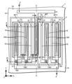
- FIG. 2 is a top view of the electrostatic discharge protection circuit shown in FIG.
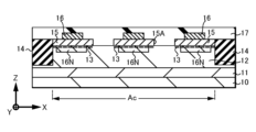
- FIG. 3 is a sectional view of a main part of the electrostatic discharge protection circuit shown in FIG. 2 (a sectional view taken along the line AA shown in FIG. 2).
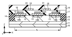
- FIG. 4 is a sectional view of a main part of the electrostatic discharge protection circuit shown in FIG. 2 (a sectional view taken along the line BB shown in FIG. 2).
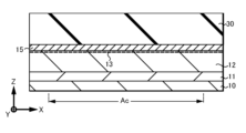
- FIG. 5 is a first step cross-sectional view (cut along the AA cutting line shown in FIG.
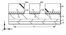
- FIG. 6 is a sectional view of the second step.
- FIG. 1 is a circuit diagram including an internal circuit of an electrostatic discharge protection circuit (ESD protection element) mounted on a semiconductor device according to a first embodiment of the present disclosure.
- FIG. 2 is a top view of the electrostatic
- FIG. 7 is a sectional view of the third step.
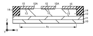
- FIG. 8 is a sectional view of the fourth step.
- FIG. 9 is a sectional view of the fifth step.
- FIG. 10 is a sectional view of the sixth step.
- FIG. 11 is a schematic plan view of the electrostatic discharge protection circuit according to the first embodiment.
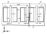
- FIG. 12 is a schematic plan view of an electrostatic discharge protection circuit according to a first comparative example.
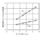
- FIG. 13 is a graph comparing the area occupied by the electrostatic discharge protection circuit according to the first embodiment and the area occupied by the electrostatic discharge protection circuit according to the first comparative example.
- FIG. 14 is a plan view corresponding to FIG. 2 of an electrostatic discharge protection circuit mounted on a semiconductor device according to a second embodiment of the present disclosure.
- FIG. 15 is a schematic plan view corresponding to FIG. 11 of the electrostatic discharge protection circuit according to the second embodiment.
- FIG. 16 is a schematic plan view corresponding to FIG. 12 of the electrostatic discharge protection circuit according to the second comparative example.
- FIG. 17 is a graph comparing the area occupied by the electrostatic discharge protection circuit according to the second embodiment and the area occupied by the electrostatic discharge protection circuit according to the second comparative example.
- FIG. 18 is a cross-sectional view of a main part of a semiconductor device and an internal circuit mounted thereon according to a third embodiment of the present disclosure.
- FIG. 19 is a cross-sectional view of a main part of a semiconductor device and an internal circuit mounted thereon according to a fourth embodiment of the present disclosure.
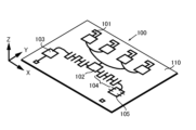
- FIG. 20 is a perspective view of a semiconductor module according to a fifth embodiment of the present disclosure.
- FIG. 21 is a block configuration diagram of an electronic device according to a sixth embodiment of the present disclosure.
- First Embodiment The first embodiment is a first example in which the present technology is applied to a semiconductor device equipped with an electrostatic discharge protection circuit. Here, the circuit configuration, planar configuration, cross-sectional configuration, and manufacturing method of the electrostatic discharge protection circuit will be described. 2. Second Embodiment The second embodiment is a second example in which the number of connected field effect transistors is increased in the electrostatic discharge protection circuit for the semiconductor device according to the first embodiment. 3. Third Embodiment The third embodiment describes the structure of an electrostatic discharge protection circuit and a monolithically constructed field effect transistor in the internal circuit of the semiconductor device according to the first embodiment or the second embodiment.
- the fourth embodiment describes the structure of an electrostatic discharge protection circuit and a monolithically constructed field effect transistor in the internal circuit of the semiconductor device according to the first embodiment or the second embodiment. This is the second example. 5.
- Fifth Embodiment The fifth embodiment is a fifth example for explaining a semiconductor module in which the semiconductor devices according to the first to fourth embodiments are mounted. 6.
- Sixth Embodiment The sixth embodiment is a sixth example for explaining an electronic device in which the semiconductor devices according to the first to fourth embodiments are mounted. 7.
- FIGS. 1 to 13 A semiconductor device 1 according to a first embodiment of the present disclosure will be described using FIGS. 1 to 13.
- the arrow X direction shown as appropriate represents one plane direction of the semiconductor device 1 placed on a plane for convenience.
- the arrow Y direction represents another plane direction orthogonal to the arrow X direction.
- the arrow Z direction represents an upward direction orthogonal to the arrow X direction and the arrow Y direction. That is, the arrow X direction, arrow Y direction, and arrow Z direction exactly correspond to the X-axis direction, Y-axis direction, and Z-axis direction, respectively, of the three-dimensional coordinate system. Note that these directions are illustrated to help understand the explanation, and do not limit the direction of the present technology.
- FIG. 1 shows an example of a circuit configuration including an electrostatic discharge protection circuit (ESD protection element) 2 and an internal circuit 5 mounted on a semiconductor device 1 according to the first embodiment. ing. As shown in FIG. 1, the semiconductor device 1 includes a first terminal 3, a second terminal 4, an internal circuit 5, and further includes an electrostatic discharge protection circuit 2.
- ESD protection element electrostatic discharge protection circuit
- the first terminal 3 is an external signal terminal to which a signal is input from outside the semiconductor device 1 .
- the first terminal 3 is electrically connected to the internal circuit 5 of the semiconductor device 1 .
- the signal is, for example, a DC signal of 2V or more and 20V or less, or -20V or more and -2V or less.
- the second terminal 4 is an external power supply terminal to which power is supplied from outside the semiconductor device 1 .
- the second terminal 4 is electrically connected to the internal circuit 5 of the semiconductor device 1 and the like.
- the power source has a fixed potential, for example, the circuit ground voltage of 0V.
- the internal circuit 5 includes field effect transistors that construct power devices, high frequency devices, etc., for example.
- the field effect transistor for example, a GaN-based hetero field effect transistor (HFET) or a GaN-based hetero junction field effect transistor (HJFET) is used. Note that, as described above, a DC signal is input to the first terminal 3, and a high frequency RF signal is not input. Therefore, even if the electrostatic discharge protection circuit 2 has poor linearity, the high frequency circuit characteristics of the internal circuit 5 will not deteriorate.
- HFET GaN-based hetero field effect transistor
- HJFET GaN-based hetero junction field effect transistor
- the electrostatic discharge protection circuit 2 is disposed between the first terminal 3 and the internal circuit 5.
- the electrostatic discharge protection circuit 2 is disposed between the first terminal 3 and the second terminal 4.
- the electrostatic discharge protection circuit 2 includes a multi-gate transistor MT as a main component. Further, the electrostatic discharge protection circuit 2 includes a resistor R electrically connected in series between the multi-gate transistor MT and the internal circuit 5.
- the multi-gate transistor MT includes a first multi-gate transistor MT1 and a second multi-gate transistor MT2.
- the first multi-gate transistor MT1 includes two first field effect transistors 21 and a second field effect transistor 22.
- the second multi-gate transistor MT2 includes two third field effect transistors 23 and a fourth field effect transistor 24.
- the first field effect transistor 21 to the fourth field effect transistor 24 of the multi-gate transistor MT are each configured to include a pair of main electrodes and a gate electrode disposed between the pair of main electrodes. . Further, in each of the first field effect transistor 21 to the fourth field effect transistor 24, the other of the pair of main electrodes and the gate electrode are electrically connected.
- One main electrode of the first field effect transistor 21 disposed at one end of the first multi-gate transistor MT1 connected in series is connected to the first terminal 3.
- the other main electrode of the first field effect transistor 21 is connected to one main electrode of a second field effect transistor 22 disposed at the other serially connected end of the first multi-gate transistor MT1.
- the other main electrode of the second field effect transistor 22 is connected to the second terminal 4. That is, the first field effect transistor 21 and the second field effect transistor 22 share the main electrode with each other and are electrically connected in series between the first terminal 3 and the second terminal 4.
- “sharing each other's main electrodes” means that one main electrode of a field effect transistor is formed in common with one main electrode of another field effect transistor, and there is no insulation separation or wiring connection, and they are integrally formed. It is used in the sense that it is composed of In other words, the first field effect transistor 21 and the second field effect transistor 22 are electrically connected in parallel between the first terminal 3 and the internal circuit 5.
- One main electrode of the third field effect transistor 23 disposed at one end of the series-connected second multi-gate transistor MT2 is connected to the first terminal 3.
- the other main electrode of the third field effect transistor 23 is connected to one main electrode of a fourth field effect transistor 24 disposed at the other series-connected end of the second multi-gate transistor MT2.
- the other main electrode of the fourth field effect transistor 24 is connected to the second terminal 4. That is, the third field effect transistor 23 and the fourth field effect transistor 24 share the main electrode with each other and are electrically connected in series between the first terminal 3 and the second terminal 4. Similarly, in other words, the third field effect transistor 23 and the fourth field effect transistor 24 are electrically connected in parallel between the first terminal 3 and the internal circuit 5.
- FIG. 2 shows an example of a planar configuration of the electrostatic discharge protection circuit 2.
- FIG. 3 shows an example of a cross-sectional configuration of the electrostatic discharge protection circuit 2.
- FIG. 4 shows an example of a cross-sectional configuration of a connection portion between the gate electrode 18 and the wiring 6 of each of the first field effect transistor 21 and the second field effect transistor 22 that constitute the electrostatic discharge protection circuit 2.
- the semiconductor device 1 includes a substrate 10 as a main component.
- a buffer layer 11 is laminated on the main surface of the substrate 10 in the direction of arrow Z.
- the first field effect transistor 21 to the fourth field effect transistor 24 are arranged on the substrate 10 with the buffer layer 11 interposed therebetween in the active region Ac within the region surrounded by the element isolation region 14.
- the first field effect transistor 21 to the fourth field effect transistor 24 include a channel layer 12, a pair of main electrodes 16, and a gate electrode 18 disposed between the pair of main electrodes 16.
- One of the pair of main electrodes 16 is used as a source electrode (source region).
- the source electrode is electrically connected to the first terminal 3.
- the other of the pair of main electrodes 16 is used as a drain electrode (drain region).
- the drain electrode is electrically connected to the second terminal 4.
- one main electrode 16 is connected to the first terminal 3, and the other main electrode 16 is shared and connected to one main electrode 16 of the second field effect transistor 22. . Further, in the first field effect transistor 21, the gate electrode 18 is connected to the other main electrode 16. A wiring 6 is used to connect the gate electrode 18 and the other main electrode 16. One end of the gate electrode 18 in the gate width direction extends to the element isolation region 14, and one end of the wiring 6 is connected to one end of the extended gate electrode 18. On the other hand, the other end of the wiring 6 extends to a region overlapping the other main electrode 16 and is connected to the other main electrode 16 in this extended region. In the second field effect transistor 22, the other main electrode 16 is connected to the second terminal 4, and the gate electrode 18 is connected to the other main electrode 16. Similar to the first field effect transistor 21, the wiring 6 is used to connect the gate electrode 18 and the other main electrode 16.
- one main electrode 16 is connected to the first terminal 3, and the other main electrode 16 is shared with one main electrode 16 of the fourth field effect transistor 24, and the other main electrode 16 is connected to the first terminal 3. has been done.
- the gate electrode 18 is connected to the other main electrode 16. Similar to the first field effect transistor 21, the wiring 6 is used to connect the gate electrode 18 and the other main electrode 16.
- the other main electrode 16 is connected to the second terminal 4, and the gate electrode 18 is connected to the other main electrode 16. Similar to the first field effect transistor 21, the wiring 6 is used to connect the gate electrode 18 and the other main electrode 16.
- the first field effect transistor 21 to the fourth field effect transistor 24 are arranged in one active region Ac surrounded by the element isolation region 14, and are configured to share the main electrode 16 with each other. That is, the first field effect transistor 21 and the second field effect transistor 22 constitute the first multi-gate transistor MT1, and the third field effect transistor 23 and the fourth field effect transistor 24 constitute the second multi-gate transistor MT2. is being built.
- a center line CC is shown between the first multi-gate transistor MT1 and the second multi-gate transistor MT2 (see FIG. 2).
- the center line CC extends in the direction of the arrow Y at the center position in the direction of the arrow X of one main electrode 16 shared by each of the first field effect transistor 21 and the third field effect transistor 23.
- the second multi-gate transistor MT2 has a line-symmetric shape with respect to the first multi-gate transistor MT1 when viewed from the direction of arrow Z (hereinafter simply referred to as "in plan view") with respect to the center line CC. is formed.
- the first multi-gate transistor MT1 and the second multi-gate transistor MT2 constitute a multi-gate transistor MT.
- the substrate 10 is made of a semiconductor material.
- the substrate 10 is made of, for example, a III-V compound semiconductor material, and here, for example, a nitride semiconductor, specifically a semi-insulating single crystal GaN substrate, is used.
- a buffer layer 11 is provided between the substrate 10 and the channel layer 12, and the lattice constant is controlled by the buffer layer 11. Therefore, a semiconductor material having a different lattice constant from that of the channel layer 12 can be used for the substrate 10.
- SiC, sapphire, Si, etc. can be used for the substrate 10 as semiconductor materials having different lattice constants.
- the buffer layer 11 is provided on the substrate 10.
- the buffer layer 11 is formed of, for example, a compound semiconductor layer grown on the substrate 10 using an epitaxial growth method. If the lattice constant of the channel layer 12 is different from the lattice constant of the substrate 10, the lattice constant can be controlled by the buffer layer 11. This improves the crystalline state of the channel layer 12, making it possible to better control warping of the substrate 10 in a wafer state.
- the buffer layer 11 can be made of, for example, AlN, AlGaN, GaN, or the like. Further, the buffer layer 11 is not limited to a single layer.
- the buffer layer 11 may be formed of a composite film in which the aforementioned AlN, AlGaN, GaN, etc. are laminated as appropriate.
- the buffer layer 11 may be formed of a ternary compound semiconductor layer whose composition is gradually changed in the thickness direction.
- a barrier layer 15 is provided on the opposite side of the channel layer 12 from the buffer layer 11 .
- the channel layer 12 is a region where carriers are accumulated due to polarization with the barrier layer 15.
- 2DEG two-dimensional electron gas
- a compound semiconductor layer is used for the channel layer 12.
- the channel layer 12 is formed of GaN, which is a nitride semiconductor.
- GaN is formed using, for example, an epitaxial growth method.
- undoped GaN (u-GaN) to which no impurities are added is used for the channel layer 12. Since no impurities are added, scattering of carriers due to impurities can be suppressed in the channel layer 12. As a result, high carrier mobility can be achieved.
- a back barrier layer may be provided between the buffer layer 11 and the channel layer 12.
- the back barrier layer is formed of a compound semiconductor material that raises the energy band on the back barrier layer side within the channel layer 12.
- the back barrier layer for example, Al 1-xy Ga x In y N (0 ⁇ x ⁇ 1, 0 ⁇ y ⁇ 1), undoped Al 1-xy Ga x In y N, etc. are practically used. can do.
- the back barrier layer is formed using an epitaxial growth method.
- the barrier layer 15 is provided in the channel layer 12.
- the barrier layer 15 is formed of a compound semiconductor material in which carriers are accumulated in the channel layer 12 due to polarization with the channel layer 12 .
- the barrier layer 15 is formed of, for example, Al 1-xy Ga x In y N (0 ⁇ x ⁇ 1, 0 ⁇ y ⁇ 1). Barrier layer 15 is formed using an epitaxial growth method.
- the barrier layer 15 may be formed of undoped Al 1-xy Ga x In y N. Since no impurities are added, scattering of carriers due to impurities in the channel layer 12 can be suppressed. As a result, high carrier mobility can be achieved. Further, the barrier layer 15 is not limited to a single layer. For example, the barrier layer 15 is formed of a composite film in which a plurality of layers with different compositions of the aforementioned Al 1-xy Ga x In y N (0 ⁇ x ⁇ 1, 0 ⁇ y ⁇ 1) are laminated. Good too. Further, the barrier layer 15 may be formed by gradually changing the composition in the thickness direction.
- a spacer layer may be provided between the channel layer 12 and the barrier layer 15.
- the spacer layer can effectively suppress scattering of carriers due to impurities and achieve high mobility.
- the spacer layer is formed of a compound semiconductor material such as Al 1-x Ga x N (0 ⁇ x ⁇ 1).
- the spacer layer may be formed of a single layer or a composite film.
- a composite film is formed by laminating a plurality of layers with different compositions of spacer layers. Further, the spacer layer may be formed by gradually changing the composition in the thickness direction.
- a gate barrier opening 15A is provided in the barrier layer 15 at an intermediate portion between the pair of main electrodes 16. There is.
- the gate barrier opening 15A is disposed at a position overlapping the gate electrode 18, and is formed here to penetrate the barrier layer 15 in the film thickness direction.
- Gate barrier opening 15A is formed by selectively etching barrier layer 15. For example, wet etching using a chemical solution having a high etching selectivity with respect to the channel layer 12 is used for the etching. Thereby, selective etching of the barrier layer 15 can be realized with high precision.
- the on-current of the first field effect transistor 21 and the like can be increased.
- the off-state current of the first field effect transistor 21 and the like can be reduced.
- the surface layer portion of the channel layer 12 may be partially etched within the gate barrier opening 15A.
- An insulator 17 is provided on the opposite side of the barrier layer 15 from the channel layer 12 and in the channel layer 12 within the gate barrier opening 15A.
- the insulator 17 is used as a gate insulating film of the first field effect transistor 21 and the like.
- the insulator 17 has insulation properties with respect to the channel layer 12 and the barrier layer 15, protects the surfaces of the channel layer 12 and the barrier layer 15 from impurities such as ions, and protects the surfaces of the channel layer 12 and the barrier layer 15 from impurities such as ions. and the barrier layer 15 to form a good interface. That is, the insulator 17 is formed of an insulating material that improves device characteristics of the first field effect transistor 21 and the like.
- the insulator 17 for example, one or more insulating materials selected from aluminum oxide (Al 2 O 3 ), hafnium oxide (HfO 2 ), silicon oxide (SiO 2 ), and silicon nitride (SiN) can be used.
- Al 2 O 3 and HfO 2 can be formed into a film by, for example, an ALD (Atomic Vapor Deposition) method.
- each of SiO 2 and SiN can be formed into a film by a CVD (Chemical Vapor Deposition) method.
- the film thickness of the insulator 17 is set to 20 nm or more in terms of oxide film equivalent film thickness. Note that the insulator 17 may be a single layer or a composite film in which a plurality of the above-selected insulating materials are laminated.
- the gate electrode 18 is disposed on the side of the insulator 17 opposite to the channel layer 12 at a position overlapping the gate barrier opening 15A.
- the gate electrode 18 is formed of a composite film in which nickel (Ni) and gold (Au) are sequentially laminated in the direction of the arrow Z. That is, the first field effect transistor 21 and the like are gate insulated field effect transistors.
- the main electrode 16 is disposed on the channel layer 12 with a barrier layer 15 interposed therebetween.
- the main electrode 16 is an ohmic electrode that forms an ohmic contact with the channel layer 12 . Thereby, the connection between the main electrode 16 and the two-dimensional electron gas 13 becomes low resistance.
- the main electrode 16 is formed of, for example, a composite film in which titanium (Ti), aluminum (Al), nickel (Ni), and gold (Au) are sequentially laminated in the direction of arrow Z.
- the main electrode 16 is connected to the two-dimensional electron gas 13 of the channel layer 12 with a high impurity density region 16N interposed between the channel layer 12 and the barrier layer 15.
- the high impurity density region 16N is disposed at a position overlapping the main electrode 16 of the channel layer 12, has the same conductivity type as the carriers flowing in the channel layer 12, and is more conductive than the channel layer 12. It is also a semiconductor region with high impurity density.
- the high impurity density region 16N is formed of an n-type semiconductor region.
- the high impurity density region 16N is formed to a deeper position on the substrate 10 side than the two-dimensional electron gas 13.
- the high impurity density region 16N is formed to have an impurity density of, for example, 10 18 atoms/cm 3 or more and 10 21 atoms/cm 3 or less. By providing the high impurity density region 16N, the connection between the main electrode 16 and the two-dimensional electron gas 13 becomes low resistance.
- the high impurity density region 16N is formed using a selective regrowth method or an ion implantation method.
- the selective regrowth method is, for example, a method in which a part of the surface of the channel layer 12 is removed by etching, and a high impurity density region 16N is selectively grown in the removed region.
- a semiconductor material such as n-In 1-x Ga x N can be used for the high impurity density region 16N.
- the ion implantation method is a method of implanting an n-type impurity into, for example, the surface portion of the channel layer 12 and activating the implanted n-type impurity.
- the element isolation region 14 is provided in the channel layer 12 and the barrier layer 15 around the active region Ac.
- the element isolation region 14 is formed using, for example, an ion implantation method.
- the ion implantation method is a method of implanting p-type impurities into the barrier layer 15 and the channel layer 12 to break the crystal and lower the conductivity.
- boron (B) is used as the p-type impurity.
- an element isolation region 14 is formed extending from the surface of the channel layer 12 to a deeper position on the substrate 10 side than the two-dimensional electron gas 13 and the high impurity density region 16N.
- the interlayer insulator 19 is disposed to cover the gate electrode 18 and the insulator 17.
- the interlayer insulator 19 is made of an insulating material that has insulation properties with respect to the gate electrode 18 and does not allow current to flow between the wirings 6 .
- Each of Al 2 O 3 and HfO 2 can be formed into a film by, for example, an ALD method.
- Each of SiO 2 and SiN can be formed into a film by a CVD method.
- the interlayer insulator 19 may be a single layer, or may be a composite film in which a plurality of the above-selected insulating materials are laminated.
- the wiring 6 is provided on the opposite side of the interlayer insulator 19 from the gate electrode 18 .
- the wiring 6 is arranged at a position overlapping the main electrode 16 of the first field effect transistor 21 and the like, and is connected to the main electrode 16 through a connection hole 19H formed in the insulator 17 and the interlayer insulator 19.
- the main electrode 16 of the first field effect transistor 21 and the like is formed in a slit shape that is short in the gate length Lg direction and long in the gate width Wg direction in plan view. Therefore, the wiring 6 passes through the connection hole 19H that overlaps most of the planar shape of the main electrode 16 and has a slit-shaped opening that is similar in shape to the main electrode 16 in plan view. connected to the majority of
- the wiring 6 connected to the other main electrode 16 of the first field effect transistor 21 is connected to the gate electrode 18 of the first field effect transistor 21. ing. One end portion of the gate electrode 18 extends into the element isolation region 14 . One end of this gate electrode 18 is connected to the wiring 6 through a connection hole 19H.
- the second field effect transistor 22 to the fourth field effect transistor 24 have a similar configuration.
- the wiring 6 is formed of a wiring material having a resistivity value smaller than that of each of the gate electrode 18 and the main electrode 16.
- one or more wiring materials selected from, for example, Ti, Pt, Al, and Au can be used.
- the resistance value of the wiring 6 between the gate electrode 18 and the main electrode 16 is set to 100 ⁇ or less. More preferably, the resistance value is set to 10 ⁇ or less.
- FIGS. 5 to 10 show examples of process cross sections explaining the manufacturing method step by step.
- the buffer layer 11 is formed on the substrate 10 (see FIG. 5).
- a Si substrate is used as the substrate 10.
- a channel layer 12 is formed on the buffer layer 11 (see FIG. 5).
- GaN is used for the channel layer 12.
- GaN is formed using an epitaxial growth method.
- a barrier layer 15 is formed on the channel layer 12 (see FIG. 5).
- u-AlGaN is used for the barrier layer 15.
- the barrier layer 15 uses Al 0.3 -Ga 0.7 N mixed crystal.
- Barrier layer 15 is formed using an epitaxial growth method. When the barrier layer 15 is formed, two-dimensional electron gas 13 is generated in the vicinity of the barrier layer 15 in the channel layer 12 .
- a mask 30 is formed on the barrier layer 15.
- the above-mentioned insulating material is used for the mask 30.
- the mask 30 is patterned. As a result, an opening 30H is formed in a portion of the mask 30 (see FIG. 6). Photolithography and etching techniques are used for patterning.
- the barrier layer 15 exposed from the opening 30H is patterned using the mask 30.
- a gate barrier opening 15A is formed in the barrier layer 15, through which the surface of the channel layer 12 is exposed.
- Etching techniques are used for patterning.
- wet etching is used which can ensure the etching selectivity between the channel layer 12 and the barrier layer 15.
- wet etching the barrier layer 15 can be selectively removed without over-etching the surface of the channel layer 12. Furthermore, since dry etching is not used, no etching damage occurs to the surface of the channel layer 12.
- patterning dry etching is first used, followed by wet etching. Furthermore, if the damage is low, patterning may be performed only by dry etching.
- the mask 30 is removed. Note that the mask 30 may be used as a protective film in subsequent steps without being removed.
- an element isolation region 14 is formed around the active region Ac.
- the element isolation region 14 is formed as a non-active region having a high resistance by, for example, implanting p-type impurities into the barrier layer 15 and the channel layer 12 by ion implantation. As a result, an island-shaped active region Ac surrounded by the element isolation region 14 is formed. Note that the element isolation region 14 may be formed after the main electrode 16 is formed or after the gate electrode 18 is formed.
- a pair of main electrodes 16 are formed in regions separated from each other on the barrier layer 15.
- the main electrode 16 is formed, for example, by sequentially depositing Ti, Al, Ni, and Au using a mask deposition method.
- an insulator 17 is formed covering the main electrode 16. Insulator 17 is also formed on barrier layer 15 and on channel layer 12 exposed from gate barrier opening 15A. In this manufacturing method, the insulator 17 is formed of, for example, SiO 2 . SiO 2 is formed using, for example, a CVD method.
- a gate electrode 18 is formed on the insulator 17 in a region overlapping the gate barrier opening 15A (see FIG. 10).
- the gate electrode 18 is formed, for example, by sequentially depositing Ni and Au using a mask deposition method.
- interlayer insulator 19 covering gate electrode 18 is formed.
- interlayer insulator 19 is formed of, for example, SiO 2 .
- SiO 2 is formed using, for example, a CVD method.
- connection holes 19H are formed in the interlayer insulator 19 (see FIGS. 2 to 4). Subsequently, as shown in FIGS. 2 to 4 described above, wiring 6 is formed on interlayer insulator 19. The wiring 6 is connected to each of the main electrode 16 and the gate electrode 18 through the connection hole 19H.
- the first to fourth field effect transistors 21 to 24 of the electrostatic discharge protection circuit 2 are formed, and the semiconductor device 1 according to the first embodiment is completed.
- the first multi-gate transistor MT1 is electrically connected in series between the first terminal 3 and the second terminal 4. That is, between the first terminal 3 and the second terminal 4, there is a capacitance C1 between one main electrode 16 and the gate electrode 18 of the first field effect transistor 21 and one main electrode 16 of the second field effect transistor 22. - The capacitance C2 between the gate electrodes 18 is electrically connected in series (see FIG. 2). Each of the capacitance C1 and the capacitance C2 is equivalent.
- the protection durability can be further improved by increasing the gate width Wg of the first to fourth field effect transistors 21 to 24.
- FIG. 11 shows an example of a schematic planar structure of the first multi-gate transistor MT1 of the electrostatic discharge protection circuit 2 according to the first embodiment.
- FIG. 12 shows an example of a schematic planar structure of a stacked transistor of the electrostatic discharge protection circuit CE according to the first comparative example.
- the first field effect transistor 21 and the second field effect transistor 22 share the main electrode 16. They are arranged in the direction of arrow X.
- the gate length Lg of each of the first field effect transistor 21 and the second field effect transistor 22 is set to, for example, 1 ⁇ m.
- the ohmic length Lo of the main electrode 16, which corresponds to the gate length Lg of each of the first field effect transistor 21 and the second field effect transistor 22, is set to, for example, 1 ⁇ m.
- the inter-gate distance Lgg1 between the gate electrode 18 of the first field effect transistor 21 and the gate electrode 18 of the second field effect transistor 22 is set to, for example, 2 ⁇ m.
- the field effect transistor 201 and the field effect transistor 202 are arranged with the element isolation region 14 interposed therebetween. They are arranged in the direction of arrow X.
- the gate length Lg of each of the field effect transistor 201 and the field effect transistor 202 is set to, for example, 1 ⁇ m.
- the ohmic length Lo of each main electrode 16 of the field effect transistor 201 and the field effect transistor 202 is set to, for example, 1 ⁇ m.
- the inter-gate distance Lgg2 between the gate electrode 18 of the field-effect transistor 201 and the gate electrode 18 of the field-effect transistor 202 is calculated by adding the dimension of one main electrode 16 and the element isolation region 14 in the arrow X direction to the inter-gate distance Lgg1. It becomes the added value.
- FIG. 13 is a graph comparing the area occupied by the electrostatic discharge protection circuit 2 according to the first embodiment and the area occupied by the electrostatic discharge protection circuit CE according to the first comparative example.
- the horizontal axis represents the ohmic length Lo [ ⁇ m].
- the vertical axis represents the area occupied by the electrostatic discharge protection circuit 2 and the electrostatic discharge protection circuit CE.
- the first multi-gate transistor MT1 of the electrostatic discharge protection circuit 2 when the total ohmic length Lo of the first field effect transistor 21 and the second field effect transistor 22 is set to 3 ⁇ m, the occupied area is “1 ” is standardized. As shown in FIG.
- the occupied area increases due to an increase in the ohmic length Lo of the field effect transistor 201 and the like and the presence of the element isolation region 14. Also in the electrostatic discharge protection circuit 2 according to the first embodiment, the occupied area increases as the ohmic length Lo of the first field effect transistor 21 and the like increases. However, the rate of increase in the area occupied by the electrostatic discharge protection circuit 2 according to the first embodiment is about 30% smaller than the rate of increase in the area occupied by the electrostatic discharge protection circuit CE according to the first comparative example. In other words, the area occupied by the electrostatic discharge protection circuit 2 according to the first embodiment is smaller than the area occupied by the electrostatic discharge protection circuit CE according to the first comparative example, regardless of the increase or decrease in the ohmic length Lo. ing.
- the semiconductor device 1 includes a multi-gate transistor MT, a first terminal 3, and a second terminal 4, as shown in FIGS. 1 to 4.
- the multi-gate transistor MT includes a first field effect transistor 21 to a fourth field effect transistor 24 having a pair of main electrodes 16 and a gate electrode 18 disposed between the pair of main electrodes 16. A plurality of the first field effect transistors 21 to fourth field effect transistors 24 share the main electrode 16 and are electrically connected in series.
- the multi-gate transistor MT includes a first multi-gate transistor MT1 and a second multi-gate transistor MT2.
- the first multi-gate transistor MT1 is constructed by a first field effect transistor 21 and a second field effect transistor 22.
- the second multi-gate transistor MT2 is constructed by the third field effect transistor 23 and the fourth field effect transistor 24. Since each of the first multi-gate transistor MT1 and the second multi-gate transistor MT2 has the same configuration, the first multi-gate transistor MT1 will be mainly explained, and the second multi-gate transistor MT2 will not be explained. The details will be explained accordingly.
- the first terminal 3 is electrically connected to one main electrode 16 of the first field effect transistor 21 at one end connected in series of the first multi-gate transistor MT1. A signal is input to the first terminal 3.
- the second terminal 4 is electrically connected to the other main electrode 16 of the second field effect transistor 22 at the other end connected in series of the first multi-gate transistor MT1. A fixed potential is supplied to the second terminal 4.
- the gate electrode 18 of at least one first field effect transistor 21 or second field effect transistor 22 of the first multi-gate transistor MT1 is connected to the other main electrode of the first field effect transistor 21 or the second field effect transistor 22. 16.
- the first multi-gate transistor MT1 (and the second multi-gate transistor MT2) construct an electrostatic discharge protection circuit 2.
- the electrostatic discharge protection circuit 2 is configured by the multi-gate transistor MT, and the main electrodes 16 of the first field effect transistor 21 to the fourth field effect transistor 24 of the multi-gate transistor MT are shared. Therefore, as shown in FIGS. 11 to 13, the area occupied by the electrostatic discharge protection circuit 2 can be reduced.
- the electrostatic breakdown voltage can be improved. That is, in the semiconductor device 1, it is possible to improve the electrostatic breakdown voltage while increasing the degree of integration.
- the gate electrodes of all the first field effect transistors 21 to fourth field effect transistors 24 of the multi-gate transistor MT constructing the electrostatic discharge protection circuit 2 are 18 is electrically connected to the other main electrode 16 of the first to fourth field effect transistors 21 to 24. Therefore, the electrostatic discharge protection circuit 2 can absorb a surge immediately when a surge is input, so that the electrostatic breakdown voltage can be further improved.
- the first field effect transistor 21 to the fourth field effect transistor 24 of the electrostatic discharge protection circuit 2 have a gate insulating film on the channel layer 12 as a semiconductor layer.
- a gate electrode 18 is formed with an insulator 17 interposed therebetween. That is, the first field effect transistor 21 to the fourth field effect transistor 24 are constituted by gate insulated field effect transistors.
- the film thickness of the insulator 17 is set to 20 nm or more in oxide film equivalent film thickness. Therefore, in the electrostatic discharge protection circuit 2, the on-state current of each of the first field effect transistor 21 to the fourth field effect transistor 24 can be increased.
- the gate electrode 18 and the other main electrode 16 have their respective specific resistance values. They are connected via a wiring 6 having a resistivity value smaller than that of the two. Therefore, the protection operation speed of the electrostatic discharge protection circuit 2 can be improved. In addition, since no resistor is inserted in the connection path between the gate electrode 18 and the main electrode 16, the area occupied by the electrostatic discharge protection circuit 2 can be further reduced.
- the main electrode 16 and the wiring 6 are connected by ohmic contact.
- the main electrode 16 is an ohmic electrode disposed on the channel layer 12 of the first field effect transistor 21 or the like.
- the ohmic electrode is electrically connected to the channel layer 12 with the high impurity density region 16N interposed therebetween.
- the high impurity density region 16N is disposed in the channel layer 12, has the same conductivity type as carriers flowing in the channel layer 12, and has a higher impurity density than the channel layer 12.
- the gate electrode 18 and the other main electrode 16 are connected at a resistance value of 100 ⁇ or less, preferably 10 ⁇ or less. In the semiconductor device 1 configured in this manner, the protection operation speed of the electrostatic discharge protection circuit 2 can be improved.
- the first field effect transistor 21 to the fourth field effect transistor 24 of the electrostatic discharge protection circuit 2 are configured to include a nitride semiconductor.
- a DC signal is input to the first terminal 3, and a reference potential (or operating power supply potential) of the high frequency circuit is supplied to the second terminal 4.
- the high frequency circuit is, for example, a power device, a high frequency device, or the like. Therefore, it is possible to realize the electrostatic discharge protection circuit 2 suitable for the semiconductor device 1 for constructing power devices, high frequency devices, and the like.
- the electrostatic discharge protection circuit 2 disposed on the signal input side of the semiconductor device 1 is described.
- the present technology may be applied to the electrostatic discharge protection circuit 2 disposed on the signal output side of the semiconductor device 1.
- a DC signal from the internal circuit 5 is output to the first terminal 3.
- the electrostatic discharge protection circuit 2 constructs a multi-gate transistor MT using a first multi-gate transistor MT1 and a second multi-gate transistor MT2 having a bilaterally symmetrical structure.
- the electrostatic discharge protection circuit 2 can control the multi-gate transistor MT by either the first multi-gate transistor MT1 or the second multi-gate transistor MT2. may be constructed.
- Second embodiment> A semiconductor device 1 and an electrostatic discharge protection circuit 2 according to a second embodiment of the present disclosure will be described using FIGS. 14 to 17.
- the same reference numerals are given to the same components or substantially the same components as those in the first embodiment, and duplications are avoided. The explanation will be omitted.
- FIG. 14 shows an example of a planar configuration of the electrostatic discharge protection circuit 2 mounted on the semiconductor device 1.
- the electrostatic discharge protection circuit 2 according to the second embodiment includes a multi-gate transistor MT.
- the multi-gate transistor MT is constructed of a first multi-gate transistor MT1 and a second multi-gate transistor MT2.
- the first multi-gate transistor MT1 further includes a fifth field effect transistor 25 in addition to the first field effect transistor 21 and the second field effect transistor 22.
- the first multi-gate transistor MT1 includes three first field effect transistors 21, three which share the main electrode 16 and are electrically connected in series between the first terminal 3 and the second terminal 4. It is composed of a second field effect transistor 22 and a fifth field effect transistor 25.
- the gate electrode 18 of each of the first field effect transistor 21, the second field effect transistor 22, and the fifth field effect transistor 25 is electrically connected to the other corresponding main electrode 16 with a wiring 6 interposed therebetween.
- the second multi-gate transistor MT2 further includes a sixth field effect transistor 26 in addition to the third field effect transistor 23 and the fourth field effect transistor 24.
- the second multi-gate transistor MT2 includes three third field effect transistors 23, three field effect transistors that share the main electrode 16 and are electrically connected in series between the first terminal 3 and the second terminal 4. It is composed of four field effect transistors 24 and a sixth field effect transistor 26.
- the gate electrode 18 of each of the third field effect transistor 23, the fourth field effect transistor 24, and the sixth field effect transistor 26 is electrically connected to the other corresponding main electrode 16 with a wiring 6 interposed therebetween.
- the second multi-gate transistor MT2 is formed in a line-symmetric shape with respect to the first multi-gate transistor MT1 with respect to the center line CC.
- FIG. 15 shows an example of a schematic planar structure of the first multi-gate transistor MT1 of the electrostatic discharge protection circuit 2 according to the second embodiment.
- FIG. 16 shows an example of a schematic planar structure of a stacked transistor of an electrostatic discharge protection circuit CE according to a second comparative example.
- the first field effect transistor 21, the second field effect transistor 22, and the fifth field effect transistor 25 are arranged in the direction of arrow X.
- the first field effect transistor 21, the second field effect transistor 22, and the fifth field effect transistor 25 each share the main electrode 16.
- the gate length Lg of each of the first field effect transistor 21, the second field effect transistor 22, and the fifth field effect transistor 25 is set to, for example, 1 ⁇ m. There is.
- the ohmic length Lo of the main electrode 16, which corresponds to the gate length Lg of each of the first field effect transistor 21, the second field effect transistor 22, and the fifth field effect transistor 25, is set to, for example, 1 ⁇ m.
- the inter-gate distance Lgg1 between the gate electrode 18 of the first field effect transistor 21 and the gate electrode 18 of the second field effect transistor 22 is set to, for example, 2 ⁇ m.
- the inter-gate distance Lgg1 between the gate electrode 18 of the second field effect transistor 22 and the gate electrode 18 of the fifth field effect transistor 25 is set to, for example, 2 ⁇ m.
- the stacked transistor of the electrostatic discharge protection circuit CE according to the second comparative example includes three field effect transistors 201, 202, and 203. There is. These field effect transistors 201, 202, and 203 are arranged in the direction of arrow X with the element isolation region 14 interposed therebetween.
- the gate length Lg of each of the field effect transistor 201, the field effect transistor 202, and the field effect transistor 203 is set to, for example, 1 ⁇ m.
- the ohmic length Lo of each main electrode 16 of the field effect transistor 201, field effect transistor 202, and field effect transistor 203 is set to, for example, 1 ⁇ m.
- the inter-gate distance Lgg2 between the gate electrode 18 of the field-effect transistor 201 and the gate electrode 18 of the field-effect transistor 202 is calculated by adding the dimension of one main electrode 16 and the element isolation region 14 in the arrow X direction to the inter-gate distance Lgg1. It becomes the added value.
- the inter-gate distance Lgg2 between the gate electrode 18 of the field-effect transistor 202 and the gate electrode 18 of the field-effect transistor 203 is equal to the inter-gate distance Lgg1 of one main electrode 16 and the element isolation region 14 in the arrow X direction.
- the value is the sum of the dimensions of
- FIG. 17 is a graph comparing the area occupied by the electrostatic discharge protection circuit 2 according to the second embodiment and the area occupied by the electrostatic discharge protection circuit CE according to the second comparative example.
- the horizontal axis represents the ohmic length Lo [ ⁇ m].
- the vertical axis represents the area occupied by the electrostatic discharge protection circuit 2 and the electrostatic discharge protection circuit CE.
- the total ohmic length Lo of the first field effect transistor 21, the second field effect transistor 22, and the fifth field effect transistor 25 is set to 3 ⁇ m.
- the occupied area is normalized to a value of "1". As shown in FIG.
- the occupied area increases as the ohmic length Lo of the field effect transistor 201 and the like increases. Also in the electrostatic discharge protection circuit 2 according to the second embodiment, the occupied area increases as the ohmic length Lo of the first field effect transistor 21 and the like increases.
- the rate of increase in the area occupied by the electrostatic discharge protection circuit 2 according to the second embodiment is about 50% smaller than the rate of increase in the area occupied by the electrostatic discharge protection circuit CE according to the second comparative example. In other words, the area occupied by the electrostatic discharge protection circuit 2 according to the second embodiment is smaller than the area occupied by the electrostatic discharge protection circuit CE according to the second comparative example, regardless of the increase or decrease in the ohmic length Lo. ing.
- the semiconductor device 1 and the electrostatic discharge protection circuit 2 according to the second embodiment obtain the same effects as those obtained by the semiconductor device 1 and the electrostatic discharge protection circuit 2 according to the first embodiment described above. be able to.
- the electrostatic discharge protection circuit 2 includes six first field effect transistors 21 to 4 that share a main electrode 16 between the first terminal 3 and the second terminal 4.
- a sixth field effect transistor 26 is provided.
- the electrostatic breakdown voltage can be further improved, and in addition, as shown in FIGS. 15 to 17, the area occupied by the electrostatic discharge protection circuit 2 can be reduced.
- the multi-gate type transistor MT is constructed with a larger number of field effect transistors connected in series than in the electrostatic discharge protection circuit 2 according to the first embodiment. Even if the number of series connections increases, the area occupied by the electrostatic discharge protection circuit 2 can be reduced compared to the electrostatic discharge protection circuit CE according to the second comparative example.
- the first multi-gate transistor MT1 of the electrostatic discharge protection circuit 2 may be constructed with four or more series connections.
- the electrostatic discharge protection circuit 2 includes a first multi-gate transistor MT1 and a second multi-gate transistor MT2 having a bilaterally symmetrical structure. We are building MT. In the present technology, if a sufficient gate width dimension can be ensured, the electrostatic discharge protection circuit 2 can control the multi-gate transistor MT by either the first multi-gate transistor MT1 or the second multi-gate transistor MT2. may be constructed.
- FIG. 18 shows an example of a cross-sectional configuration of the internal circuit 5.
- the first field effect transistor 21 to the fourth field effect transistor 24 of the multi-gate transistor MT of the electrostatic discharge protection circuit 2 according to the first embodiment, and the internal circuit 5 A field effect transistor 27 (see FIG. 1) is constructed monolithically.
- the field effect transistor 27 basically has a structure similar to that of the first field effect transistor 21 to the fourth field effect transistor 24, and here, the field effect transistor 27 is a depletion type field effect transistor exhibiting normally-on operation. It is composed of a transistor (DFET: Depression type Field Effect Transistor).
- DFET Depression type Field Effect Transistor
- the gate barrier opening 15A is not provided in the barrier layer 15 (see FIG. 3). That is, in the field effect transistor 27, the gate electrode 18 is provided on the channel layer 12 with the barrier layer 15 and the insulator 17 interposed therebetween.
- the "barrier layer 15" corresponds to the "semiconductor layer” according to the present technology.
- a two-dimensional electron gas 13 is formed at a position of the channel layer 12 overlapping the gate electrode 18 when the channel layer 12 is in the off state.
- the internal circuit 5 according to the third embodiment is monolithically constructed with the first field effect transistor 21 to the sixth field effect transistor 26 of the multi-gate transistor MT of the electrostatic discharge protection circuit 2 according to the second embodiment.
- the field effect transistor 27 may also be configured as a field effect transistor 27.
- the semiconductor device 1 and internal circuit 5 according to the third embodiment have the same effects as the semiconductor device 1 and the electrostatic discharge protection circuit 2 according to the first or second embodiment described above. Effects can be obtained.
- the field effect transistor 27 of the internal circuit 5 is monolithically configured with the multi-gate transistor MT of the electrostatic discharge protection circuit 2 according to the first embodiment or the second embodiment described above. be done.
- the semiconductor device 1 can be constructed using a simple structure and manufacturing method.
- FIG. 19 shows an example of a cross-sectional configuration of the internal circuit 5.
- the internal circuit 5 according to the fourth embodiment includes a field effect transistor 27 similarly to the internal circuit 5 according to the third embodiment.
- the field effect transistor 27 has a T-type gate structure.
- the gate barrier opening 15A is not provided in the barrier layer 15, as in the field effect transistor 27 of the internal circuit 5 according to the third embodiment (see FIG. (See 3).
- a gate opening 7A penetrating through the insulator 17 in the film thickness direction is provided at a position overlapping the gate electrode 18.
- a gate insulating film 7 is provided at least on the barrier layer 15 exposed from the gate opening 7A. That is, in the field effect transistor 27, the gate electrode 18 is disposed within the gate opening 7A with the gate insulating film 7 interposed in the barrier layer 15.
- the "barrier layer 15" corresponds to the "semiconductor layer” according to the present technology.
- the gate electrode 18 is formed to have a larger dimension in the gate length Lg direction and gate width Wg direction than the opening dimension of the gate opening 7A. That is, in a side view, the cross section of the gate electrode 18 is formed in a T-shape.
- the internal circuit 5 according to the fourth embodiment is monolithically constructed with the first field effect transistor 21 to the sixth field effect transistor 26 of the multi-gate transistor MT of the electrostatic discharge protection circuit 2 according to the second embodiment.
- the field effect transistor 27 may also be configured as a field effect transistor 27.
- the semiconductor device 1 and internal circuit 5 according to the fourth embodiment can provide the same effects as those obtained by the semiconductor device 1 and internal circuit 5 according to the third embodiment described above.
- the field effect transistor 27 of the internal circuit 5 is monolithically configured with the multi-gate type transistor MT of the electrostatic discharge protection circuit 2 according to the first embodiment or the second embodiment described above. be done.
- the semiconductor device 1 can be constructed using a simple structure and manufacturing method.
- FIG. 20 shows a schematic structure of a semiconductor module 100 according to the fifth embodiment.
- the semiconductor module 100 is an antenna integrated module in which, for example, an edge antenna 101 arranged in an array and a front end component are mounted on a substrate 110 as one module.
- the front end components include a switch 102, a low noise amplifier 103, a bandpass filter 104, a power amplifier 105, and the like.
- the semiconductor module 100 can be used, for example, as a communication transceiver.
- the semiconductor module 100 includes one of the semiconductor devices 1 according to the first to fourth embodiments as transistors that constitute the switch 102, the low noise amplifier 103, the power amplifier 105, etc., for example.
- the semiconductor module 100 according to the fifth embodiment includes the semiconductor device 1, it is possible to achieve even higher speed, higher efficiency, and lower power consumption of wireless communication. Further, the electrostatic discharge protection circuit 2 according to any one of the first to fourth embodiments is mounted on the semiconductor device 1. Therefore, in the semiconductor module 100, it is possible to reduce the area occupied by the electrostatic discharge protection circuit 2 while improving resistance to electrostatic discharge protection.
- FIG. 21 shows a schematic block configuration of a wireless communication device 300 according to the sixth embodiment.
- the wireless communication device 300 includes an antenna ANT, an antenna switch circuit 301, a high power amplifier HPA, a radio frequency integrated circuit (RFIC), a baseband section BB, and an audio output section. It includes a MIC, a data output section DT, and an interface section I/F.
- the interface unit I/F includes, for example, a wireless LAN (W-LAN: Wireless Local Area Network), Bluetooth (registered trademark), and the like.
- the wireless communication device 300 is, for example, a mobile phone system having multiple functions such as voice, data communication, and LAN connection.
- the wireless communication device 300 is a semiconductor device according to any one of the first to fourth embodiments as a transistor constituting an antenna switch circuit 301, a high power amplifier HPA, a high frequency integrated circuit RFIC, or a baseband section BB. 1.
- the wireless communication device 300 according to the sixth embodiment includes the semiconductor device 1, it is possible to realize even higher speed, higher efficiency, and lower power consumption of wireless communication. Therefore, when the wireless communication device 300 is a mobile communication terminal, the usage time of the wireless communication device 300 can be further extended, so that portability can be further improved. Further, the electrostatic discharge protection circuit 2 according to any one of the first to fourth embodiments is mounted on the semiconductor device 1. Therefore, in the wireless communication device 300, it is possible to reduce the area occupied by the electrostatic discharge protection circuit 2 while improving resistance to electrostatic discharge protection.
- the transistor is made of a GaN-based semiconductor.
- the present technology is applicable to a semiconductor device in which a transistor is configured using a GaAs-based, InP-based, or SiGe-based compound semiconductor. Further, the present technology is also applicable to a semiconductor device in which a transistor is configured using a Si semiconductor. Further, in the present technology, a Schottky junction field effect transistor may be used as the field effect transistor of the electrostatic discharge protection circuit.
- the semiconductor device includes a multi-gate transistor, a first terminal, and a second terminal.
- a multi-gate transistor a plurality of field effect transistors each having a pair of main electrodes and a gate electrode disposed between the pair of main electrodes are electrically connected in series while sharing the main electrodes.
- the first terminal is electrically connected to one main electrode of a field effect transistor at one end connected in series of the multi-gate transistor.
- a signal is input or output to the first terminal.
- the second terminal is electrically connected to the other main electrode of the field effect transistor at the other end of the multi-gate transistor connected in series. A fixed potential is supplied to the second terminal.
- the gate electrode of at least one field effect transistor of the multi-gate transistor is electrically connected to the other main electrode of the field effect transistor.
- the multi-gate transistor constitutes an electrostatic breakdown protection circuit. For this reason, an electrostatic discharge protection circuit in which a plurality of field effect transistors are electrically connected in series is provided between the first terminal and the second terminal, so that the electrostatic breakdown protection withstand voltage can be improved. . In addition, since the plurality of field effect transistors are multi-gate transistors and share a main electrode, the area occupied by the electrostatic breakdown protection circuit can be reduced.
- a semiconductor module according to a second embodiment of the present disclosure includes a semiconductor device.
- the semiconductor device is a semiconductor device according to the first embodiment. Therefore, in the semiconductor module, the same effects as those obtained by the semiconductor device according to the first embodiment can be obtained.
- An electronic device includes a semiconductor device.
- the semiconductor device is a semiconductor device according to the first embodiment. Therefore, in the electronic device, the same effects as those obtained by the semiconductor device according to the first embodiment can be obtained.
- the present technology has the following configuration. According to the present technology having the following configuration, in a semiconductor device, a semiconductor module, and an electronic device, the electrostatic breakdown protection withstand voltage can be improved, and the area occupied by the electrostatic breakdown protection circuit can be reduced.
- a multi-gate type transistor in which a plurality of field effect transistors each having a pair of main electrodes and a gate electrode disposed between the pair of main electrodes are electrically connected in series while sharing the main electrodes; a first terminal electrically connected to one of the main electrodes of the field effect transistors at one end connected in series of the multi-gate transistors, and into which a signal is input or output; a second terminal electrically connected to the other main electrode of the field effect transistor at the other end connected in series of the multi-gate transistor and supplied with a fixed potential;
- a semiconductor device wherein the gate electrode of at least one field effect transistor of the multi-gate transistor is electrically connected to the main electrode of the other field effect transistor.
- the other main electrode and the wiring are connected by ohmic junction.
- the other main electrode is an ohmic electrode disposed in the channel layer of the field effect transistor, The ohmic electrode is disposed in the channel layer, has the same conductivity type as carriers flowing in the channel layer, and is connected to the channel layer with a high impurity density region interposed therebetween, which has a higher impurity density than the channel layer.
- the semiconductor device according to (5) or (6) above which is electrically connected.
- the semiconductor device according to any one of (1) to (8), wherein the field effect transistor includes a nitride semiconductor.
- a DC signal is input or output to the first terminal, The semiconductor device according to any one of (1) to (9), wherein the second terminal is supplied with an operating power supply potential or a reference potential of a high-frequency circuit.
- the high frequency circuit is a power amplifier.
- the multi-gate transistor constitutes an electrostatic breakdown protection circuit.
- the semiconductor device includes: A multi-gate type transistor in which a plurality of field effect transistors each having a pair of main electrodes and a gate electrode disposed between the pair of main electrodes are electrically connected in series while sharing the main electrodes; a first terminal electrically connected to one of the main electrodes of the field effect transistors at one end connected in series of the multi-gate transistors, and into which a signal is input or output; a second terminal electrically connected to the other main electrode of the field effect transistor at the other end connected in series of the multi-gate transistor and supplied with a fixed potential;
- the semiconductor module wherein the gate electrode of at least one field effect transistor of the multi-gate transistor is electrically connected to the main electrode of the other field effect transistor.
- the semiconductor device includes: A multi-gate type transistor in which a plurality of field effect transistors each having a pair of main electrodes and a gate electrode disposed between the pair of main electrodes are electrically connected in series while sharing the main electrodes; a first terminal electrically connected to one of the main electrodes of the field effect transistors at one end connected in series of the multi-gate transistors, and into which a signal is input or output; a second terminal electrically connected to the other main electrode of the field effect transistor at the other end connected in series of the multi-gate transistor and supplied with a fixed potential; An electronic device, wherein the gate electrode of at least one field effect transistor of the multi-gate transistor is electrically connected to the main electrode of the other field effect transistor.
Landscapes
- Junction Field-Effect Transistors (AREA)
- Electronic Switches (AREA)
- Metal-Oxide And Bipolar Metal-Oxide Semiconductor Integrated Circuits (AREA)
Abstract
半導体装置は、一対の主電極及び一対の主電極間に配設されたゲート電極を有する電界効果トランジスタが、互いに主電極を共有して電気的に直列に複数接続されたマルチゲート型トランジスタと、マルチゲート型トランジスタの直列に接続された一端の電界効果トランジスタの一方の主電極に電気的に接続され、信号が入力又は出力される第1端子と、マルチゲート型トランジスタの直列に接続された他端の電界効果トランジスタの他方の主電極に電気的に接続され、固定電位が供給される第2端子とを備えている。マルチゲート型トランジスタの少なくとも1つの電界効果トランジスタのゲート電極は、当該電界効果トランジスタの他方の主電極に電気的に接続されている。
Description
本開示は、半導体装置、半導体モジュール及び電子機器に関する。
ワイドギャップ半導体材料として、GaNが使用されている。GaNにより製作されるデバイスでは、絶縁破壊電圧が高く、高温動作が可能であり、飽和ドリフト速度が速い等の特徴がある。また、GaN系ヘテロ接合に生成される二次元電子ガス(2DEG)においては、移動度が高く、かつ、シート電子密度が高いという特徴がある。
これらの特徴により、GaN系ヘテロFET(HFET)では、低抵抗、高速動作、高耐圧動作が可能である。このため、パワーデバイスや高周波(RF)デバイス等への適用が期待されている。
これらの特徴により、GaN系ヘテロFET(HFET)では、低抵抗、高速動作、高耐圧動作が可能である。このため、パワーデバイスや高周波(RF)デバイス等への適用が期待されている。
GaN等の化合物半導体を用いた高周波デバイスでは、一般に、高周波特性に優れているが、静電気放電(ESD:Electro Static Discharge)破壊に対して弱い。このため、静電気放電破壊の対策が望まれている。
下記特許文献1には、静電保護回路が開示されている。静電保護回路は、外部端子と電源端子との間に配置され、一方のドレインと他方のソースとを接続して電気的に直列に接続された複数のMOS(Metal Oxide Semiconductor)トランジスタを備えている。複数のMOSトランジスタのそれぞれのゲート電極は、ソースに接続されている。また、複数のMOSトランジスタは、各々、素子分離により電気的に分離されている。
このように構成される静電保護回路では、外部端子に印加される静電気が複数のMOSトランジスタに分圧される。このため、静電気放電破壊耐圧を向上させることができる。
下記特許文献1には、静電保護回路が開示されている。静電保護回路は、外部端子と電源端子との間に配置され、一方のドレインと他方のソースとを接続して電気的に直列に接続された複数のMOS(Metal Oxide Semiconductor)トランジスタを備えている。複数のMOSトランジスタのそれぞれのゲート電極は、ソースに接続されている。また、複数のMOSトランジスタは、各々、素子分離により電気的に分離されている。
このように構成される静電保護回路では、外部端子に印加される静電気が複数のMOSトランジスタに分圧される。このため、静電気放電破壊耐圧を向上させることができる。
上記静電保護回路では、複数のMOSトランジスタが素子分離により分離されているので、MOSトランジスタの接続数が増加すれば、占有面積が増大する。このため、パワートランジスタ、高周波デバイス等を構築する半導体装置では、DC信号が印加される外部端子に配設される静電気破壊保護回路において、静電気破壊耐圧を向上させ、かつ、占有面積を縮小させることが望まれていた。
本開示の第1実施態様に係る半導体装置は、一対の主電極及び一対の主電極間に配設されたゲート電極を有する電界効果トランジスタが、互いに主電極を共有して電気的に直列に複数接続されたマルチゲート型トランジスタと、マルチゲート型トランジスタの直列に接続された一端の電界効果トランジスタの一方の主電極に電気的に接続され、信号が入力又は出力される第1端子と、マルチゲート型トランジスタの直列に接続された他端の電界効果トランジスタの他方の主電極に電気的に接続され、固定電位が供給される第2端子とを備え、マルチゲート型トランジスタの少なくとも1つの電界効果トランジスタのゲート電極が、当該電界効果トランジスタの他方の主電極に電気的に接続されている。
ここで、マルチゲート型トランジスタは、静電気破壊保護回路を構成している。
ここで、マルチゲート型トランジスタは、静電気破壊保護回路を構成している。
本開示の第2実施態様に係る半導体モジュールは、半導体装置を備え、半導体装置は、一対の主電極及び一対の主電極間に配設されたゲート電極を有する電界効果トランジスタが、互いに主電極を共有して電気的に直列に複数接続されたマルチゲート型トランジスタと、マルチゲート型トランジスタの直列に接続された一端の電界効果トランジスタの一方の主電極に電気的に接続され、信号が入力又は出力される第1端子と、マルチゲート型トランジスタの直列に接続された他端の電界効果トランジスタの他方の主電極に電気的に接続され、固定電位が供給される第2端子とを備え、マルチゲート型トランジスタの少なくとも1つの電界効果トランジスタのゲート電極が、当該電界効果トランジスタの他方の主電極に電気的に接続されている。
本開示の第3実施態様に係る電子機器は、半導体装置を備え、半導体装置は、一対の主電極及び一対の主電極間に配設されたゲート電極を有する電界効果トランジスタが、互いに主電極を共有して電気的に直列に複数接続されたマルチゲート型トランジスタと、マルチゲート型トランジスタの直列に接続された一端の電界効果トランジスタの一方の主電極に電気的に接続され、信号が入力又は出力される第1端子と、マルチゲート型トランジスタの直列に接続された他端の電界効果トランジスタの他方の主電極に電気的に接続され、固定電位が供給される第2端子とを備え、マルチゲート型トランジスタの少なくとも1つの電界効果トランジスタのゲート電極が、当該電界効果トランジスタの他方の主電極に電気的に接続されている。
以下、本開示の実施の形態について図面を参照して詳細に説明する。なお、説明は以下の順序で行う。
1.第1実施の形態
第1実施の形態は、静電気放電保護回路が搭載された半導体装置に、本技術を適用した第1例である。ここでは、静電気放電保護回路の回路構成、平面構成、断面構成及び製造方法について説明する。
2.第2実施の形態
第2実施の形態は、第1実施の形態に係る半導体装置の静電気放電保護回路において、電界効果トランジスタの接続数を増加した第2例である。
3.第3実施の形態
第3実施の形態は、第1実施の形態又は第2実施の形態に係る半導体装置の内部回路において、静電気放電保護回路とモノリシックに構築された電界効果トランジスタの構造を説明する第1例である。
4.第4実施の形態
第4実施の形態は、第1実施の形態又は第2実施の形態に係る半導体装置の内部回路において、静電気放電保護回路とモノリシックに構築された電界効果トランジスタの構造を説明する第2例である。
5.第5実施の形態
第5実施の形態は、第1実施の形態~第4実施の形態に係る半導体装置を実装した半導体モジュールを説明する第5例である。
6.第6実施の形態
第6実施の形態は、第1実施の形態~第4実施の形態に係る半導体装置を実装した電子機器を説明する第6例である。
7.その他の実施の形態
1.第1実施の形態
第1実施の形態は、静電気放電保護回路が搭載された半導体装置に、本技術を適用した第1例である。ここでは、静電気放電保護回路の回路構成、平面構成、断面構成及び製造方法について説明する。
2.第2実施の形態
第2実施の形態は、第1実施の形態に係る半導体装置の静電気放電保護回路において、電界効果トランジスタの接続数を増加した第2例である。
3.第3実施の形態
第3実施の形態は、第1実施の形態又は第2実施の形態に係る半導体装置の内部回路において、静電気放電保護回路とモノリシックに構築された電界効果トランジスタの構造を説明する第1例である。
4.第4実施の形態
第4実施の形態は、第1実施の形態又は第2実施の形態に係る半導体装置の内部回路において、静電気放電保護回路とモノリシックに構築された電界効果トランジスタの構造を説明する第2例である。
5.第5実施の形態
第5実施の形態は、第1実施の形態~第4実施の形態に係る半導体装置を実装した半導体モジュールを説明する第5例である。
6.第6実施の形態
第6実施の形態は、第1実施の形態~第4実施の形態に係る半導体装置を実装した電子機器を説明する第6例である。
7.その他の実施の形態
<1.第1実施の形態>
図1~図13を用いて、本開示の第1実施の形態に係る半導体装置1を説明する。
ここで、図中、適宜、示されている矢印X方向は、便宜的に平面上に載置された半導体装置1の1つの平面方向を表している。矢印Y方向は、矢印X方向に対して直交する他の1つの平面方向を表している。また、矢印Z方向は、矢印X方向及び矢印Y方向に対して直交する上方向を表している。つまり、矢印X方向、矢印Y方向、矢印Z方向は、丁度、三次元座標系のX軸方向、Y軸方向、Z軸方向に各々一致している。
なお、これらの各方向は、説明の理解を助けるために図示したものであり、本技術の方向を限定するものではない。
図1~図13を用いて、本開示の第1実施の形態に係る半導体装置1を説明する。
ここで、図中、適宜、示されている矢印X方向は、便宜的に平面上に載置された半導体装置1の1つの平面方向を表している。矢印Y方向は、矢印X方向に対して直交する他の1つの平面方向を表している。また、矢印Z方向は、矢印X方向及び矢印Y方向に対して直交する上方向を表している。つまり、矢印X方向、矢印Y方向、矢印Z方向は、丁度、三次元座標系のX軸方向、Y軸方向、Z軸方向に各々一致している。
なお、これらの各方向は、説明の理解を助けるために図示したものであり、本技術の方向を限定するものではない。
[半導体装置1及び静電気放電保護回路2の回路構成]
(1)半導体装置1の全体構成
図1は、第1実施の形態に係る半導体装置1に搭載された静電気放電保護回路(ESD保護素子)2の及び内部回路5を含む回路構成の一例を表している。
図1に示されるように、半導体装置1は、第1端子3と、第2端子4と、内部回路5とを備え、更に静電気放電保護回路2を備えている。
(1)半導体装置1の全体構成
図1は、第1実施の形態に係る半導体装置1に搭載された静電気放電保護回路(ESD保護素子)2の及び内部回路5を含む回路構成の一例を表している。
図1に示されるように、半導体装置1は、第1端子3と、第2端子4と、内部回路5とを備え、更に静電気放電保護回路2を備えている。
第1端子3は、半導体装置1の外部から信号が入力される外部信号端子である。第1端子3は、半導体装置1の内部回路5に電気的に接続されている。信号は、例えば2V以上20V以下、又は-20V以上-2V以下のDC信号である。
第2端子4は、半導体装置1の外部から電源が供給される外部電源端子である。第2端子4は、半導体装置1の内部回路5等に電気的に接続されている。電源は、固定電位、例えば回路の接地電圧0Vである。
第2端子4は、半導体装置1の外部から電源が供給される外部電源端子である。第2端子4は、半導体装置1の内部回路5等に電気的に接続されている。電源は、固定電位、例えば回路の接地電圧0Vである。
内部回路5は、第1実施の形態において、例えばパワーデバイス、高周波デバイス等を構築する電界効果トランジスタを備えている。電界効果トランジスタとしては、例えばGaN系ヘテロ電界効果トランジスタ(HFET:Hetero Field Effect Transistor)又はGaN系ヘテロ接合電界効果トランジスタ(HJFET:Hetero junction Field Effect Transistor)が使用されている。
なお、前述の通り、第1端子3にはDC信号が入力され、高周波RF信号が入力されない。このため、静電気放電保護回路2のリニアリティが悪くても、内部回路5の高周波回路特性を劣化させることがない。
なお、前述の通り、第1端子3にはDC信号が入力され、高周波RF信号が入力されない。このため、静電気放電保護回路2のリニアリティが悪くても、内部回路5の高周波回路特性を劣化させることがない。
(2)静電気放電保護回路2の回路構成
静電気放電保護回路2は、第1端子3と内部回路5との間に配設されている。また、表現を代えれば、静電気放電保護回路2は、第1端子3と第2端子4との間に配設されている。
静電気放電保護回路2は、マルチゲート型トランジスタMTを主要な構成要素として備えている。さらに、静電気放電保護回路2は、マルチゲート型トランジスタMTと内部回路5との間に、電気的に直列に接続された抵抗Rを備えている。
静電気放電保護回路2は、第1端子3と内部回路5との間に配設されている。また、表現を代えれば、静電気放電保護回路2は、第1端子3と第2端子4との間に配設されている。
静電気放電保護回路2は、マルチゲート型トランジスタMTを主要な構成要素として備えている。さらに、静電気放電保護回路2は、マルチゲート型トランジスタMTと内部回路5との間に、電気的に直列に接続された抵抗Rを備えている。
マルチゲート型トランジスタMTは、第1実施の形態において、第1マルチゲート型トランジスタMT1と、第2マルチゲート型トランジスタMT2とを備えている。第1マルチゲート型トランジスタMT1は、2個の第1電界効果トランジスタ21及び第2電界効果トランジスタ22を備えている。第2マルチゲート型トランジスタMT2は、2個の第3電界効果トランジスタ23及び第4電界効果トランジスタ24を備えている。
マルチゲート型トランジスタMTの第1電界効果トランジスタ21~第4電界効果トランジスタ24は、いずれも、一対の主電極と、一対の主電極間に配設されたゲート電極とを含んで構成されている。さらに、第1電界効果トランジスタ21~第4電界効果トランジスタ24では、いずれも、一対の主電極のうちの他方の主電極とゲート電極とが電気的に接続されている。
マルチゲート型トランジスタMTの第1電界効果トランジスタ21~第4電界効果トランジスタ24は、いずれも、一対の主電極と、一対の主電極間に配設されたゲート電極とを含んで構成されている。さらに、第1電界効果トランジスタ21~第4電界効果トランジスタ24では、いずれも、一対の主電極のうちの他方の主電極とゲート電極とが電気的に接続されている。
第1マルチゲート型トランジスタMT1の直列に接続された一端に配設された第1電界効果トランジスタ21の一方の主電極は、第1端子3に接続されている。第1電界効果トランジスタ21の他方の主電極は、第1マルチゲート型トランジスタMT1の直列に接続された他端に配設された第2電界効果トランジスタ22の一方の主電極に接続されている。そして、第2電界効果トランジスタ22の他方の主電極は、第2端子4に接続されている。つまり、第1電界効果トランジスタ21及び第2電界効果トランジスタ22は、互いの主電極を共有し、第1端子3と第2端子4との間に電気的に直列に接続されている。
ここで、「互いの主電極を共有する」とは、電界効果トランジスタの1つの主電極が他の電界効果トランジスタの1つの主電極と共通に形成され、絶縁分離や配線による接続が無く、一体に構成されているという意味において使用されている。
また、表現を代えれば、第1電界効果トランジスタ21及び第2電界効果トランジスタ22は、第1端子3と内部回路5との間に電気的に並列に接続されている。
ここで、「互いの主電極を共有する」とは、電界効果トランジスタの1つの主電極が他の電界効果トランジスタの1つの主電極と共通に形成され、絶縁分離や配線による接続が無く、一体に構成されているという意味において使用されている。
また、表現を代えれば、第1電界効果トランジスタ21及び第2電界効果トランジスタ22は、第1端子3と内部回路5との間に電気的に並列に接続されている。
第2マルチゲート型トランジスタMT2の直列に接続された一端に配設された第3電界効果トランジスタ23の一方の主電極は、第1端子3に接続されている。第3電界効果トランジスタ23の他方の主電極は、第2マルチゲート型トランジスタMT2の直列に接続された他端に配設された第4電界効果トランジスタ24の一方の主電極に接続されている。そして、第4電界効果トランジスタ24の他方の主電極は、第2端子4に接続されている。つまり、第3電界効果トランジスタ23及び第4電界効果トランジスタ24は、互いの主電極を共有し、第1端子3と第2端子4との間に電気的に直列に接続されている。
同様に、表現を代えれば、第3電界効果トランジスタ23及び第4電界効果トランジスタ24は、第1端子3と内部回路5との間に電気的に並列に接続されている。
同様に、表現を代えれば、第3電界効果トランジスタ23及び第4電界効果トランジスタ24は、第1端子3と内部回路5との間に電気的に並列に接続されている。
[静電気放電保護回路2の具体的なデバイス構成]
(1)第1電界効果トランジスタ21~第4電界効果トランジスタ24の構成
図2は、静電気放電保護回路2の平面構成の一例を表している。図3は、静電気放電保護回路2の断面構成の一例を表している。図4は、静電気放電保護回路2を構成する第1電界効果トランジスタ21、第2電界効果トランジスタ22のそれぞれのゲート電極18と配線6との接続部の断面構成の一例を表している。
(1)第1電界効果トランジスタ21~第4電界効果トランジスタ24の構成
図2は、静電気放電保護回路2の平面構成の一例を表している。図3は、静電気放電保護回路2の断面構成の一例を表している。図4は、静電気放電保護回路2を構成する第1電界効果トランジスタ21、第2電界効果トランジスタ22のそれぞれのゲート電極18と配線6との接続部の断面構成の一例を表している。
第1実施の形態に係る半導体装置1は、主要な構成要素として、基板10を備えている。基板10の主面には、矢印Z方向に向かってバッファ層11が積層されている。
第1電界効果トランジスタ21~第4電界効果トランジスタ24は、素子分離領域14に周囲を囲まれた領域内のアクティブ領域Acにおいて、基板10にバッファ層11を介在して配設されている。
第1電界効果トランジスタ21~第4電界効果トランジスタ24は、素子分離領域14に周囲を囲まれた領域内のアクティブ領域Acにおいて、基板10にバッファ層11を介在して配設されている。
すなわち、第1電界効果トランジスタ21~第4電界効果トランジスタ24は、チャネル層12と、一対の主電極16と、一対の主電極16間に配設されたゲート電極18とを備えている。一対の主電極16の一方は、ソース電極(ソース領域)として使用される。ここでは、ソース電極は、第1端子3に電気的に接続されている。一対の主電極16の他方は、ドレイン電極(ドレイン領域)として使用される。ドレイン電極は、第2端子4に電気的に接続されている。
第1電界効果トランジスタ21では、一方の主電極16が第1端子3に接続され、他方の主電極16が第2電界効果トランジスタ22の一方の主電極16に共有され、かつ、接続されている。
さらに、第1電界効果トランジスタ21では、ゲート電極18が他方の主電極16に接続されている。ゲート電極18と他方の主電極16との接続には、配線6が使用されている。ゲート電極18のゲート幅方向の一端部は素子分離領域14まで延設され、この延設されたゲート電極18の一端部に配線6の一端部が接続されている。一方、配線6の他端部は、他方の主電極16に重複する領域まで延設され、この延設された領域において他方の主電極16に接続されている。
第2電界効果トランジスタ22では、他方の主電極16が第2端子4に接続され、ゲート電極18が他方の主電極16に接続されている。ゲート電極18と他方の主電極16との接続には、第1電界効果トランジスタ21と同様に、配線6が使用されている。
さらに、第1電界効果トランジスタ21では、ゲート電極18が他方の主電極16に接続されている。ゲート電極18と他方の主電極16との接続には、配線6が使用されている。ゲート電極18のゲート幅方向の一端部は素子分離領域14まで延設され、この延設されたゲート電極18の一端部に配線6の一端部が接続されている。一方、配線6の他端部は、他方の主電極16に重複する領域まで延設され、この延設された領域において他方の主電極16に接続されている。
第2電界効果トランジスタ22では、他方の主電極16が第2端子4に接続され、ゲート電極18が他方の主電極16に接続されている。ゲート電極18と他方の主電極16との接続には、第1電界効果トランジスタ21と同様に、配線6が使用されている。
同様に、第3電界効果トランジスタ23では、一方の主電極16が第1端子3に接続され、他方の主電極16が第4電界効果トランジスタ24の一方の主電極16に共有され、かつ、接続されている。さらに、第3電界効果トランジスタ23では、ゲート電極18が他方の主電極16に接続されている。ゲート電極18と他方の主電極16との接続には、第1電界効果トランジスタ21と同様に、配線6が使用されている。
第4電界効果トランジスタ24では、他方の主電極16が第2端子4に接続され、ゲート電極18が他方の主電極16に接続されている。ゲート電極18と他方の主電極16との接続には、第1電界効果トランジスタ21と同様に、配線6が使用されている。
第4電界効果トランジスタ24では、他方の主電極16が第2端子4に接続され、ゲート電極18が他方の主電極16に接続されている。ゲート電極18と他方の主電極16との接続には、第1電界効果トランジスタ21と同様に、配線6が使用されている。
第1電界効果トランジスタ21~第4電界効果トランジスタ24は、素子分離領域14により周囲が取り囲まれた1つのアクティブ領域Acに配設され、互いの主電極16を共有して構成されている。つまり、第1電界効果トランジスタ21及び第2電界効果トランジスタ22は、第1マルチゲート型トランジスタMT1を構築し、第3電界効果トランジスタ23及び第4電界効果トランジスタ24は、第2マルチゲート型トランジスタMT2を構築している。
第1マルチゲート型トランジスタMT1と第2マルチゲート型トランジスタMT2との間には、便宜的に中心線C-Cが示されている(図2参照)。中心線C-Cは、第1電界効果トランジスタ21、第3電界効果トランジスタ23のそれぞれに共有される一方の主電極16の矢印X方向の中心位置において、矢印Y方向に延設されている。中心線C-Cを中心として、第2マルチゲート型トランジスタMT2は、第1マルチゲート型トランジスタMT1に対して、矢印Z方向から見て(以下、単に「平面視において」という。)線対称形状に形成されている。
そして、第1マルチゲート型トランジスタMT1及び第2マルチゲート型トランジスタMT2は、マルチゲート型トランジスタMTを構築している。
第1マルチゲート型トランジスタMT1と第2マルチゲート型トランジスタMT2との間には、便宜的に中心線C-Cが示されている(図2参照)。中心線C-Cは、第1電界効果トランジスタ21、第3電界効果トランジスタ23のそれぞれに共有される一方の主電極16の矢印X方向の中心位置において、矢印Y方向に延設されている。中心線C-Cを中心として、第2マルチゲート型トランジスタMT2は、第1マルチゲート型トランジスタMT1に対して、矢印Z方向から見て(以下、単に「平面視において」という。)線対称形状に形成されている。
そして、第1マルチゲート型トランジスタMT1及び第2マルチゲート型トランジスタMT2は、マルチゲート型トランジスタMTを構築している。
(2)基板10の構成
基板10は、半導体材料が使用されている。詳しく説明すると、基板10には、例えばIII-V族化合物半導体材料が使用され、ここでは、例えば窒化物半導体、具体的には半絶縁性の単結晶GaN基板が使用されている。
また、第1実施の形態では、基板10とチャネル層12との間にバッファ層11が配設され、バッファ層11により格子定数が制御されている。このため、基板10には、チャネル層12に対して格子定数が異なる半導体材料が使用可能である。例えば、格子定数が異なる半導体材料として、例えばSiC、サファイア、Si等を基板10に使用することができる。
基板10は、半導体材料が使用されている。詳しく説明すると、基板10には、例えばIII-V族化合物半導体材料が使用され、ここでは、例えば窒化物半導体、具体的には半絶縁性の単結晶GaN基板が使用されている。
また、第1実施の形態では、基板10とチャネル層12との間にバッファ層11が配設され、バッファ層11により格子定数が制御されている。このため、基板10には、チャネル層12に対して格子定数が異なる半導体材料が使用可能である。例えば、格子定数が異なる半導体材料として、例えばSiC、サファイア、Si等を基板10に使用することができる。
(3)バッファ層11の構成
バッファ層11は、基板10に配設されている。バッファ層11には、例えば基板10上にエピタキシャル成長法を用いて成長させた化合物半導体層により形成されている。
基板10の格子定数に対して、チャネル層12の格子定数が異なる場合には、バッファ層11により格子定数を制御することができる。これにより、チャネル層12の結晶状態が良好になり、ウエハ状態の基板10の反りを良好に制御することができる。
バッファ層11は、基板10に配設されている。バッファ層11には、例えば基板10上にエピタキシャル成長法を用いて成長させた化合物半導体層により形成されている。
基板10の格子定数に対して、チャネル層12の格子定数が異なる場合には、バッファ層11により格子定数を制御することができる。これにより、チャネル層12の結晶状態が良好になり、ウエハ状態の基板10の反りを良好に制御することができる。
例えば、基板10が単結晶Si基板により形成され、チャネル層12がGaNにより形成される場合、バッファ層11には、例えばAlN、AlGaN、GaN等を使用することができる。
また、バッファ層11は単層に限定されない。例えば、バッファ層11は、前述のAlN、AlGaN、GaN等を適宜積層した複合膜により形成してもよい。さらに、バッファ層11は、膜厚方向において、徐々に組成を変化させた3元系化合物半導体層により形成してもよい。
また、バッファ層11は単層に限定されない。例えば、バッファ層11は、前述のAlN、AlGaN、GaN等を適宜積層した複合膜により形成してもよい。さらに、バッファ層11は、膜厚方向において、徐々に組成を変化させた3元系化合物半導体層により形成してもよい。
(4)チャネル層12の構成
チャネル層12のバッファ層11とは反対側には、バリア層15が配設されている。チャネル層12は、バリア層15との分極によりキャリアが蓄積される領域である。チャネル層12において、バリア層15の近傍には、キャリアが蓄積され、キャリアのチャネル領域として機能する二次元電子ガス(2DEG)13が生成される。
チャネル層12には、化合物半導体層が使用されている。例えば、チャネル層12は、窒化物半導体であるGaNにより形成されている。GaNは、例えばエピタキシャル成長法を用いて形成されている。ここでは、不純物が添加されていないアンドープGaN(u-GaN)が、チャネル層12に使用されている。不純物が添加されていないので、チャネル層12ではキャリアの不純物による散乱を抑制することができる。結果的に、キャリアの高移動度を実現することができる。
チャネル層12のバッファ層11とは反対側には、バリア層15が配設されている。チャネル層12は、バリア層15との分極によりキャリアが蓄積される領域である。チャネル層12において、バリア層15の近傍には、キャリアが蓄積され、キャリアのチャネル領域として機能する二次元電子ガス(2DEG)13が生成される。
チャネル層12には、化合物半導体層が使用されている。例えば、チャネル層12は、窒化物半導体であるGaNにより形成されている。GaNは、例えばエピタキシャル成長法を用いて形成されている。ここでは、不純物が添加されていないアンドープGaN(u-GaN)が、チャネル層12に使用されている。不純物が添加されていないので、チャネル層12ではキャリアの不純物による散乱を抑制することができる。結果的に、キャリアの高移動度を実現することができる。
なお、バッファ層11とチャネル層12との間に、バックバリア層が配設されてもよい。バックバリア層は、チャネル層12内のバックバリア層側のエネルギバンドを持ち上げる化合物半導体材料により形成されている。バックバリア層を備えると、第1電界効果トランジスタ21~第4電界効果トランジスタ24において、短チャネル効果等を効果的に抑制することができる。
バックバリア層としては、例えばAl1-x-yGaxInyN(0≦x<1、0≦y<1)、アンドープAl1-x-yGaxInyN等を実用的に使用することができる。バックバリア層は、エピタキシャル成長法を用いて形成されている。
バックバリア層としては、例えばAl1-x-yGaxInyN(0≦x<1、0≦y<1)、アンドープAl1-x-yGaxInyN等を実用的に使用することができる。バックバリア層は、エピタキシャル成長法を用いて形成されている。
(5)バリア層15の構成
バリア層15は、前述の通り、チャネル層12に配設されている。バリア層15は、チャネル層12との分極によりチャネル層12内にキャリアが蓄積される化合物半導体材料により形成されている。バリア層15は、例えばAl1-x-yGaxInyN(0≦x<1、0≦y<1)により形成されている。バリア層15は、エピタキシャル成長法を用いて形成されている。
バリア層15は、前述の通り、チャネル層12に配設されている。バリア層15は、チャネル層12との分極によりチャネル層12内にキャリアが蓄積される化合物半導体材料により形成されている。バリア層15は、例えばAl1-x-yGaxInyN(0≦x<1、0≦y<1)により形成されている。バリア層15は、エピタキシャル成長法を用いて形成されている。
また、バリア層15は、アンドープAl1-x-yGaxInyNにより形成されてもよい。不純物が添加されていないので、チャネル層12においてキャリアの不純物による散乱を抑制することができる。結果的に、キャリアの高移動度を実現することができる。
また、バリア層15は単層に限定されない。例えば、バリア層15は、前述のAl1-x-yGaxInyN(0≦x<1、0≦y<1)の組成を変えた複数の層を積層した複合膜により形成してもよい。さらに、バリア層15は、膜厚方向において、徐々に組成を変化させて形成してもよい。
また、バリア層15は単層に限定されない。例えば、バリア層15は、前述のAl1-x-yGaxInyN(0≦x<1、0≦y<1)の組成を変えた複数の層を積層した複合膜により形成してもよい。さらに、バリア層15は、膜厚方向において、徐々に組成を変化させて形成してもよい。
なお、図示は省略するが、チャネル層12とバリア層15との間に、スペーサ層が配設されてもよい。スペーサ層は、キャリアの不純物による散乱を効果的に抑制し、高移動度を実現可能である。
スペーサ層は、例えばAl1-xGaxN(0≦x<1)等の化合物半導体材料により形成されている。スペーサ層は、単層により形成されてもよいし、複合膜により形成されてもよい。複合膜は、スペーサ層の組成を変えた複数の層を積層して形成されている。また、スペーサ層は、膜厚方向において、徐々に組成を変化させて形成してもよい。
スペーサ層は、例えばAl1-xGaxN(0≦x<1)等の化合物半導体材料により形成されている。スペーサ層は、単層により形成されてもよいし、複合膜により形成されてもよい。複合膜は、スペーサ層の組成を変えた複数の層を積層して形成されている。また、スペーサ層は、膜厚方向において、徐々に組成を変化させて形成してもよい。
平面視において、又は矢印Y方向に見て(以下、単に「側面視において」という。)、一対の主電極16間の中間部分において、バリア層15には、ゲートバリア開口15Aが配設されている。ゲートバリア開口15Aは、ゲート電極18に重複する位置に配設され、ここではバリア層15を膜厚方向に貫通して形成されている。
ゲートバリア開口15Aは、バリア層15を選択的にエッチングすることにより形成されている。エッチングには、例えば、チャネル層12に対してエッチング選択比が高い薬液を用いたウエットエッチングが使用される。これにより、高精度において、バリア層15の選択的なエッチングを実現することができる。
ゲートバリア開口15Aは、バリア層15を選択的にエッチングすることにより形成されている。エッチングには、例えば、チャネル層12に対してエッチング選択比が高い薬液を用いたウエットエッチングが使用される。これにより、高精度において、バリア層15の選択的なエッチングを実現することができる。
なお、前述のスペーサ層をゲートバリア開口15A内に残存させた構成では、第1電界効果トランジスタ21等のオン電流を高くすることができる。
逆に、ゲートバリア開口15A内のスペーサ層が完全に除去された構成では、第1電界効果トランジスタ21等のオフ電流を低減することができる。この構成の場合、ゲートバリア開口15A内において、チャネル層12の表層部が部分的にエッチングされていてもよい。
逆に、ゲートバリア開口15A内のスペーサ層が完全に除去された構成では、第1電界効果トランジスタ21等のオフ電流を低減することができる。この構成の場合、ゲートバリア開口15A内において、チャネル層12の表層部が部分的にエッチングされていてもよい。
(6)絶縁体17の構成
バリア層15のチャネル層12とは反対側及びゲートバリア開口15A内のチャネル層12には、絶縁体17が配設されている。絶縁体17は、第1電界効果トランジスタ21等のゲート絶縁膜として使用されている。詳しく説明すると、絶縁体17は、チャネル層12及びバリア層15に対して絶縁性を有し、イオン等の不純物に対してチャネル層12及びバリア層15の表面を保護し、かつ、チャネル層12及びバリア層15との間に良好な界面を形成する。すなわち、絶縁体17は、第1電界効果トランジスタ21等のデバイス特性を向上させる絶縁材料により形成されている。
バリア層15のチャネル層12とは反対側及びゲートバリア開口15A内のチャネル層12には、絶縁体17が配設されている。絶縁体17は、第1電界効果トランジスタ21等のゲート絶縁膜として使用されている。詳しく説明すると、絶縁体17は、チャネル層12及びバリア層15に対して絶縁性を有し、イオン等の不純物に対してチャネル層12及びバリア層15の表面を保護し、かつ、チャネル層12及びバリア層15との間に良好な界面を形成する。すなわち、絶縁体17は、第1電界効果トランジスタ21等のデバイス特性を向上させる絶縁材料により形成されている。
絶縁体17としては、例えば、酸化アルミニウム(Al2O3)、酸化ハフニウム(HfO2)、酸化シリコン(SiO2)及び窒化シリコン(SiN)から選択される1以上の絶縁材料を使用することができる。Al2O3、HfO2のそれぞれは、例えばALD(Atomic Vapor Deposition)法により成膜可能である。また、SiO2、SiNのそれぞれは、CVD(Chemical Vapor Deposition)法により成膜可能である。絶縁体17の膜厚は、酸化膜換算膜厚において、20nm以上に設定されている。
なお、絶縁体17は、単層であっても、上記選択された絶縁材料を複数積層した複合膜であってもよい。
なお、絶縁体17は、単層であっても、上記選択された絶縁材料を複数積層した複合膜であってもよい。
(7)ゲート電極18の構成
ゲート電極18は、ゲートバリア開口15Aに重複する位置において、絶縁体17のチャネル層12とは反対側に配設されている。ゲート電極18は、ここでは、矢印Z方向に向かって、ニッケル(Ni)、金(Au)のそれぞれを順次積層した複合膜により形成されている。
すなわち、第1電界効果トランジスタ21等は、ゲート絶縁型電界効果トランジスタである。
ゲート電極18は、ゲートバリア開口15Aに重複する位置において、絶縁体17のチャネル層12とは反対側に配設されている。ゲート電極18は、ここでは、矢印Z方向に向かって、ニッケル(Ni)、金(Au)のそれぞれを順次積層した複合膜により形成されている。
すなわち、第1電界効果トランジスタ21等は、ゲート絶縁型電界効果トランジスタである。
(8)主電極16の構成
主電極16は、チャネル層12にバリア層15を介在させて配設されている。主電極16は、チャネル層12に対してオーミック接合(オーミック接触)となるオーミック電極である。これにより、主電極16と二次元電子ガス13との接続は低抵抗になる。
主電極16は、例えば、矢印Z方向に向かって、チタン(Ti)、アルミニウム(Al)、ニッケル(Ni)、金(Au)のそれぞれを順次積層した複合膜により形成されている。
主電極16は、チャネル層12にバリア層15を介在させて配設されている。主電極16は、チャネル層12に対してオーミック接合(オーミック接触)となるオーミック電極である。これにより、主電極16と二次元電子ガス13との接続は低抵抗になる。
主電極16は、例えば、矢印Z方向に向かって、チタン(Ti)、アルミニウム(Al)、ニッケル(Ni)、金(Au)のそれぞれを順次積層した複合膜により形成されている。
さらに、主電極16は、チャネル層12とバリア層15との間に配設された高不純物密度領域16Nを介在させて、チャネル層12の二次元電子ガス13に接続されている。平面視並びに側面視において、高不純物密度領域16Nは、チャネル層12の主電極16に重複する位置に配設され、チャネル層12に流れるキャリアと同一導電型を有し、かつ、チャネル層12よりも不純物密度が高い半導体領域である。
第1実施の形態において、二次元電子ガス13にはキャリアとして電子が流れるので、高不純物密度領域16Nはn型半導体領域により形成されている。高不純物密度領域16Nは、二次元電子ガス13よりも基板10側に深い位置まで形成されている。高不純物密度領域16Nは、例えば1018原子/cm3以上1021原子/cm3以下の不純物密度に形成されている。
高不純物密度領域16Nを備えることにより、主電極16と二次元電子ガス13との接続は低抵抗になる。
第1実施の形態において、二次元電子ガス13にはキャリアとして電子が流れるので、高不純物密度領域16Nはn型半導体領域により形成されている。高不純物密度領域16Nは、二次元電子ガス13よりも基板10側に深い位置まで形成されている。高不純物密度領域16Nは、例えば1018原子/cm3以上1021原子/cm3以下の不純物密度に形成されている。
高不純物密度領域16Nを備えることにより、主電極16と二次元電子ガス13との接続は低抵抗になる。
高不純物密度領域16Nは、選択再成長法、又はイオン注入法を用いて形成されている。
選択再成長法は、例えば、チャネル層12の表面の一部をエッチングにより取り除き、この取り除かれた領域に高不純物密度領域16Nを選択的に成長させる方法である。この場合、高不純物密度領域16Nには、n-In1-xGaxN等の半導体材料が使用可能である。
一方、イオン注入法は、例えばチャネル層12の表面部分に、n型不純物を注入し、注入されたn型不純物を活性化する方法である。
選択再成長法は、例えば、チャネル層12の表面の一部をエッチングにより取り除き、この取り除かれた領域に高不純物密度領域16Nを選択的に成長させる方法である。この場合、高不純物密度領域16Nには、n-In1-xGaxN等の半導体材料が使用可能である。
一方、イオン注入法は、例えばチャネル層12の表面部分に、n型不純物を注入し、注入されたn型不純物を活性化する方法である。
(9)素子分離領域14の構成
素子分離領域14は、アクティブ領域Acの周囲において、チャネル層12及びバリア層15に配設されている。素子分離領域14は、例えばイオン注入法を用いて形成されている。イオン注入法は、バリア層15及びチャネル層12にp型不純物を注入し、結晶を壊して導電性を下げる方法である。p型不純物としては、例えば硼素(B)が使用されている。チャネル層12では、チャネル層12の表面から二次元電子ガス13、更には高不純物密度領域16Nよりも基板10側に深い位置にわたって素子分離領域14が形成されている。
素子分離領域14は、アクティブ領域Acの周囲において、チャネル層12及びバリア層15に配設されている。素子分離領域14は、例えばイオン注入法を用いて形成されている。イオン注入法は、バリア層15及びチャネル層12にp型不純物を注入し、結晶を壊して導電性を下げる方法である。p型不純物としては、例えば硼素(B)が使用されている。チャネル層12では、チャネル層12の表面から二次元電子ガス13、更には高不純物密度領域16Nよりも基板10側に深い位置にわたって素子分離領域14が形成されている。
(10)層間絶縁体19の構成
層間絶縁体19は、ゲート電極18及び絶縁体17を覆って配設されている。層間絶縁体19は、ゲート電極18に対して絶縁性を有し、配線6間に電流を流さない絶縁材料により形成されている。層間絶縁体19としては、絶縁体17と同様に、例えばAl2O3、HfO2、SiO2及びSiNから選択される1以上の絶縁材料を使用することができる。Al2O3、HfO2のそれぞれは、例えばALD法により成膜可能である。SiO2、SiNのそれぞれは、CVD法により成膜可能である。
なお、層間絶縁体19は、単層であっても、上記選択された複数の絶縁材料を複数積層した複合膜であってもよい。
層間絶縁体19は、ゲート電極18及び絶縁体17を覆って配設されている。層間絶縁体19は、ゲート電極18に対して絶縁性を有し、配線6間に電流を流さない絶縁材料により形成されている。層間絶縁体19としては、絶縁体17と同様に、例えばAl2O3、HfO2、SiO2及びSiNから選択される1以上の絶縁材料を使用することができる。Al2O3、HfO2のそれぞれは、例えばALD法により成膜可能である。SiO2、SiNのそれぞれは、CVD法により成膜可能である。
なお、層間絶縁体19は、単層であっても、上記選択された複数の絶縁材料を複数積層した複合膜であってもよい。
(11)配線6の構成
配線6は、層間絶縁体19のゲート電極18とは反対側に配設されている。配線6は、第1電界効果トランジスタ21等の主電極16に重複する位置に配設され、絶縁体17及び層間絶縁体19に形成された接続孔19Hを通して主電極16に接続されている。
第1実施の形態では、平面視において、第1電界効果トランジスタ21等の主電極16は、ゲート長Lg方向に短く、ゲート幅Wg方向に長いスリット形状に形成されている。このため、配線6は、主電極16の平面形状の大半に重複して配置され、かつ、平面視において主電極16に対して相似形状であるスリット形状の開口を有する接続孔19Hを通して主電極16の大半に接続されている。
配線6は、層間絶縁体19のゲート電極18とは反対側に配設されている。配線6は、第1電界効果トランジスタ21等の主電極16に重複する位置に配設され、絶縁体17及び層間絶縁体19に形成された接続孔19Hを通して主電極16に接続されている。
第1実施の形態では、平面視において、第1電界効果トランジスタ21等の主電極16は、ゲート長Lg方向に短く、ゲート幅Wg方向に長いスリット形状に形成されている。このため、配線6は、主電極16の平面形状の大半に重複して配置され、かつ、平面視において主電極16に対して相似形状であるスリット形状の開口を有する接続孔19Hを通して主電極16の大半に接続されている。
また、第1実施の形態に係る静電気放電保護回路2では、第1電界効果トランジスタ21の他方の主電極16に接続された配線6は、この第1電界効果トランジスタ21のゲート電極18に接続されている。ゲート電極18の一端部は、素子分離領域14に延設されている。このゲート電極18の一端部が、接続孔19Hを通して配線6に接続されている。
第2電界効果トランジスタ22~第4電界効果トランジスタ24についても同様の構成とされている。
第2電界効果トランジスタ22~第4電界効果トランジスタ24についても同様の構成とされている。
配線6は、ゲート電極18、主電極16のそれぞれの比抵抗値よりも小さい比抵抗値を有する配線材料により形成されている。配線6としては、例えばTi、Pt、Al及びAuから選択される1以上の配線材料を使用することができる。ここでは、ゲート電極18と主電極16との間の配線6の抵抗値は、100Ω以下に設定されている。さらに好ましくは、抵抗値が10Ω以下に設定されている。
[半導体装置1及び静電気放電保護回路2の製造方法]
次に、第1実施の形態に係る半導体装置1及び静電気放電保護回路2の製造方法を説明する。図5~図10は、製造方法を工程毎に説明する工程断面の一例を表している。
次に、第1実施の形態に係る半導体装置1及び静電気放電保護回路2の製造方法を説明する。図5~図10は、製造方法を工程毎に説明する工程断面の一例を表している。
まず、基板10上にバッファ層11が形成される(図5参照)。基板10には、例えばSi基板が使用される。
次に、バッファ層11上にチャネル層12が形成される(図5参照)。チャネル層12には、例えばGaNが使用される。GaNは、エピタキシャル成長法を用いて形成される。
次に、バッファ層11上にチャネル層12が形成される(図5参照)。チャネル層12には、例えばGaNが使用される。GaNは、エピタキシャル成長法を用いて形成される。
次に、チャネル層12上にバリア層15が形成される(図5参照)。バリア層15には、例えばu-AlGaNが使用される。例えば、バリア層15には、Al0.3-Ga0.7N混晶が使用される。バリア層15は、エピタキシャル成長法を用いて形成される。
バリア層15が形成されると、チャネル層12においてバリア層15の近傍に二次元電子ガス13が生成される。
バリア層15が形成されると、チャネル層12においてバリア層15の近傍に二次元電子ガス13が生成される。
図5に示されるように、バリア層15上にマスク30が形成される。マスク30には、例えば前述の絶縁材料が使用される。
次に、マスク30がパターンニングされる。これにより、マスク30の一部に開口30Hが形成される(図6参照)。パターンニングには、フォトリソグラフィ技術及びエッチング技術が使用される。
図6に示されるように、マスク30を用いて、開口30Hから露出するバリア層15がパターンニングされる。このパターンニングにより、バリア層15にはチャネル層12の表面が露出するゲートバリア開口15Aが形成される。
パターンニングにはエッチング技術が使用される。エッチング技術では、チャネル層12とバリア層15とのエッチング選択比を確保可能なウエットエッチングが使用される。ウエットエッチングを使用することにより、チャネル層12の表面がオーバエッチングされることなく、バリア層15を選択的に除去することができる。また、ドライエッチングが使用されていないので、チャネル層12の表面のエッチングダメージが生じない。
パターンニングにはエッチング技術が使用される。エッチング技術では、チャネル層12とバリア層15とのエッチング選択比を確保可能なウエットエッチングが使用される。ウエットエッチングを使用することにより、チャネル層12の表面がオーバエッチングされることなく、バリア層15を選択的に除去することができる。また、ドライエッチングが使用されていないので、チャネル層12の表面のエッチングダメージが生じない。
なお、パターンニングには、最初にドライエッチングを用い、引き続きウエットエッチングが使用される。また、低ダメージであれば、ドライエッチングのみでパターンニングが行われてもよい。
次に、マスク30が除去される。なお、マスク30は、除去せずに、これ以降の工程において保護膜として使用してもよい。
図7に示されるように、アクティブ領域Acの周囲において、素子分離領域14が形成される。素子分離領域14は、例えばp型不純物をイオン注入法によりバリア層15及びチャネル層12に注入し、高抵抗化された非アクティブ領域として形成される。これにより、素子分離領域14に周囲が取り囲まれた島状のアクティブ領域Acが形成される。
なお、素子分離領域14は、主電極16の形成後、又はゲート電極18の形成後に形成してもよい。
なお、素子分離領域14は、主電極16の形成後、又はゲート電極18の形成後に形成してもよい。
図8に示されるように、バリア層15上の互いに離間された領域に一対の主電極16が形成される。主電極16は、例えば、マスク蒸着法を用いて、Ti、Al、Ni、Auのそれぞれを順次蒸着することにより形成される。
図9に示されるように、主電極16を覆って絶縁体17が形成される。絶縁体17は、バリア層15上及びゲートバリア開口15Aから露出されるチャネル層12上にも形成される。この製造方法では、絶縁体17は、例えばSiO2により形成される。SiO2は例えばCVD法を用いて形成される。
次に、ゲートバリア開口15Aに重複する領域において、絶縁体17上にゲート電極18が形成される(図10参照)。ゲート電極18は、例えば、マスク蒸着法を用いて、Ni、Auのそれぞれを順次蒸着することにより形成される。
図10に示されるように、ゲート電極18を覆う層間絶縁体19が形成される。この製造方法では、層間絶縁体19は、例えばSiO2により形成される。SiO2は例えばCVD法を用いて形成される。
次に、層間絶縁体19に接続孔19Hが形成される(図2~図4参照)。引き続き、前述の図2~図4に示されるように、層間絶縁体19上に配線6が形成される。配線6は、接続孔19Hを通して主電極16、ゲート電極18のそれぞれに接続される。
これら一連の製造工程が終了すると、静電気放電保護回路2の第1電界効果トランジスタ21~第4電界効果トランジスタ24が形成され、第1実施の形態に係る半導体装置1が完成する。
[静電気放電保護回路2の動作]
前述の図1~図4を用いて、静電気放電保護回路2の保護動作について簡単に説明する。ここでは、第1マルチゲート型トランジスタMT1の保護動作について説明する。第1マルチゲート型トランジスタMT1の保護動作と同一であるので、第2マルチゲート型トランジスタMT2の保護動作についての説明は省略する。
前述の図1~図4を用いて、静電気放電保護回路2の保護動作について簡単に説明する。ここでは、第1マルチゲート型トランジスタMT1の保護動作について説明する。第1マルチゲート型トランジスタMT1の保護動作と同一であるので、第2マルチゲート型トランジスタMT2の保護動作についての説明は省略する。
第1マルチゲート型トランジスタMT1は、第1端子3と第2端子4との間に電気的に直列に接続されている。つまり、第1端子3と第2端子4との間には、第1電界効果トランジスタ21の一方の主電極16-ゲート電極18間容量C1と、第2電界効果トランジスタ22の一方の主電極16-ゲート電極18間容量C2とが電気的に直列に接続されている(図2参照)。容量C1、容量C2のそれぞれは、等価である。
ここで、第1端子3にサージが印加されたと仮定する。サージは、容量C1、容量C2のそれぞれに瞬時に分圧される。この分圧に伴い、第1マルチゲート型トランジスタMT1の第1電界効果トランジスタ21及び第2電界効果トランジスタ22は、一方の主電極16とゲート電極18との間に同一の電圧が印加されるので、オン状態になる。
このため、第1端子3に印加されたサージは、第1電界効果トランジスタ21及び第2電界効果トランジスタ22を流れて第2端子4に吸収される。
このため、第1端子3に印加されたサージは、第1電界効果トランジスタ21及び第2電界効果トランジスタ22を流れて第2端子4に吸収される。
なお、静電気放電保護回路2において、第1電界効果トランジスタ21~第4電界効果トランジスタ24のゲート幅Wg寸法を長くすれば、保護耐性をより一層向上させることができる。
[静電気放電保護回路2の特徴]
図11は、第1実施の形態に係る静電気放電保護回路2の第1マルチゲート型トランジスタMT1の模式的な平面構造の一例を表している。図12は、第1比較例に係る静電気放電保護回路CEのスタック型トランジスタの模式的な平面構造の一例を表している。
図11は、第1実施の形態に係る静電気放電保護回路2の第1マルチゲート型トランジスタMT1の模式的な平面構造の一例を表している。図12は、第1比較例に係る静電気放電保護回路CEのスタック型トランジスタの模式的な平面構造の一例を表している。
図11に示されるように、第1実施の形態に係る静電気放電保護回路2の第1マルチゲート型トランジスタMT1では、第1電界効果トランジスタ21及び第2電界効果トランジスタ22が、主電極16を共有して、矢印X方向に配列されている。
ここで、第1電界効果トランジスタ21、第2電界効果トランジスタ22のそれぞれのゲート長Lgは、例えば1μmに設定されている。また、第1電界効果トランジスタ21、第2電界効果トランジスタ22のそれぞれのゲート長Lgに一致する主電極16のオーミック長Loは、例えば1μmに設定されている。第1電界効果トランジスタ21のゲート電極18と第2電界効果トランジスタ22のゲート電極18との間のゲート間距離Lgg1は、例えば2μmに設定されている。
ここで、第1電界効果トランジスタ21、第2電界効果トランジスタ22のそれぞれのゲート長Lgは、例えば1μmに設定されている。また、第1電界効果トランジスタ21、第2電界効果トランジスタ22のそれぞれのゲート長Lgに一致する主電極16のオーミック長Loは、例えば1μmに設定されている。第1電界効果トランジスタ21のゲート電極18と第2電界効果トランジスタ22のゲート電極18との間のゲート間距離Lgg1は、例えば2μmに設定されている。
これに対して、図12に示されるように、第1比較例に係る静電気放電保護回路CEのスタック型トランジスタでは、電界効果トランジスタ201及び電界効果トランジスタ202が、素子分離領域14を介在して、矢印X方向に配列されている。
ここで、電界効果トランジスタ201、電界効果トランジスタ202のそれぞれのゲート長Lgは、例えば1μmに設定されている。また、電界効果トランジスタ201、電界効果トランジスタ202のそれぞれの主電極16のオーミック長Loは、例えば1μmに設定されている。電界効果トランジスタ201のゲート電極18と電界効果トランジスタ202のゲート電極18との間のゲート間距離Lgg2は、ゲート間距離Lgg1に、1つの主電極16及び素子分離領域14の矢印X方向の寸法を加算した値になる。
ここで、電界効果トランジスタ201、電界効果トランジスタ202のそれぞれのゲート長Lgは、例えば1μmに設定されている。また、電界効果トランジスタ201、電界効果トランジスタ202のそれぞれの主電極16のオーミック長Loは、例えば1μmに設定されている。電界効果トランジスタ201のゲート電極18と電界効果トランジスタ202のゲート電極18との間のゲート間距離Lgg2は、ゲート間距離Lgg1に、1つの主電極16及び素子分離領域14の矢印X方向の寸法を加算した値になる。
図13は、第1実施の形態に係る静電気放電保護回路2の占有面積と第1比較例に係る静電気放電保護回路CEの占有面積とを比較したグラフである。横軸は、オーミック長Lo[μm]を表している。縦軸は、静電気放電保護回路2、静電気放電保護回路CEのそれぞれの占有面積を表している。ここで、静電気放電保護回路2の第1マルチゲート型トランジスタMT1において、第1電界効果トランジスタ21及び第2電界効果トランジスタ22の合計のオーミック長Loが3μmに設定されるとき、占有面積が「1」の値に規格化されている。
図13に示されるように、第1比較例に係る静電気放電保護回路CEでは、電界効果トランジスタ201等のオーミック長Loの増加並びに素子分離領域14の存在に伴い、占有面積が増加する。
第1実施の形態に係る静電気放電保護回路2でも、第1電界効果トランジスタ21等のオーミック長Loの増加に伴い、占有面積が増加する。しかしながら、第1比較例に係る静電気放電保護回路CEの占有面積の増加率に対して、第1実施の形態に係る静電気放電保護回路2の占有面積の増加率は約30%程度少ない。表現を代えれば、第1実施の形態に係る静電気放電保護回路2の占有面積は、第1比較例に係る静電気放電保護回路CEの占有面積に対して、オーミック長Loの増減に関係無く縮小されている。
図13に示されるように、第1比較例に係る静電気放電保護回路CEでは、電界効果トランジスタ201等のオーミック長Loの増加並びに素子分離領域14の存在に伴い、占有面積が増加する。
第1実施の形態に係る静電気放電保護回路2でも、第1電界効果トランジスタ21等のオーミック長Loの増加に伴い、占有面積が増加する。しかしながら、第1比較例に係る静電気放電保護回路CEの占有面積の増加率に対して、第1実施の形態に係る静電気放電保護回路2の占有面積の増加率は約30%程度少ない。表現を代えれば、第1実施の形態に係る静電気放電保護回路2の占有面積は、第1比較例に係る静電気放電保護回路CEの占有面積に対して、オーミック長Loの増減に関係無く縮小されている。
[作用効果]
第1実施の形態に係る半導体装置1は、図1~図4に示されるように、マルチゲート型トランジスタMTと、第1端子3と、第2端子4とを備える。
マルチゲート型トランジスタMTは、一対の主電極16及び一対の主電極16間に配設されたゲート電極18を有する第1電界効果トランジスタ21~第4電界効果トランジスタ24を備える。第1電界効果トランジスタ21~第4電界効果トランジスタ24は、互いに主電極16を共有して電気的に直列に複数接続される。
ここで、マルチゲート型トランジスタMTは、第1マルチゲート型トランジスタMT1及び第2マルチゲート型トランジスタMT2を備える。第1マルチゲート型トランジスタMT1は、第1電界効果トランジスタ21及び第2電界効果トランジスタ22により構築される。また、第2マルチゲート型トランジスタMT2は、第3電界効果トランジスタ23及び第4電界効果トランジスタ24により構築される。第1マルチゲート型トランジスタMT1、第2マルチゲート型トランジスタMT2のそれぞれは同一構成であるので、第1マルチゲート型トランジスタMT1について主体的に説明し、第2マルチゲート型トランジスタMT2の説明は必要に応じて適宜説明する。
第1端子3は、第1マルチゲート型トランジスタMT1の直列に接続された一端の第1電界効果トランジスタ21の一方の主電極16に電気的に接続される。第1端子3には、信号が入力される。
第2端子4は、第1マルチゲート型トランジスタMT1の直列に接続された他端の第2電界効果トランジスタ22の他方の主電極16に電気的に接続される。第2端子4には、固定電位が供給される。
そして、第1マルチゲート型トランジスタMT1の少なくとも1つの第1電界効果トランジスタ21又は第2電界効果トランジスタ22のゲート電極18が、第1電界効果トランジスタ21又は第2電界効果トランジスタ22の他方の主電極16に電気的に接続される。
第1マルチゲート型トランジスタMT1(及び第2マルチゲート型トランジスタMT2)は、静電気放電保護回路2を構築する。
このように構成される半導体装置1では、静電気放電保護回路2がマルチゲート型トランジスタMTにより構成され、マルチゲート型トランジスタMTの第1電界効果トランジスタ21~第4電界効果トランジスタ24の主電極16が共有される。このため、図11~図13に示されるように、静電気放電保護回路2の占有面積を縮小するこができる。加えて、このように構成される静電気放電保護回路2では、複数の第1電界効果トランジスタ21~第4電界効果トランジスタ24が直列に接続されているので、静電気破壊耐圧を向上させることができる。つまり、半導体装置1では、集積度を向上させつつ、静電気破壊耐圧を向上させることができる。
第1実施の形態に係る半導体装置1は、図1~図4に示されるように、マルチゲート型トランジスタMTと、第1端子3と、第2端子4とを備える。
マルチゲート型トランジスタMTは、一対の主電極16及び一対の主電極16間に配設されたゲート電極18を有する第1電界効果トランジスタ21~第4電界効果トランジスタ24を備える。第1電界効果トランジスタ21~第4電界効果トランジスタ24は、互いに主電極16を共有して電気的に直列に複数接続される。
ここで、マルチゲート型トランジスタMTは、第1マルチゲート型トランジスタMT1及び第2マルチゲート型トランジスタMT2を備える。第1マルチゲート型トランジスタMT1は、第1電界効果トランジスタ21及び第2電界効果トランジスタ22により構築される。また、第2マルチゲート型トランジスタMT2は、第3電界効果トランジスタ23及び第4電界効果トランジスタ24により構築される。第1マルチゲート型トランジスタMT1、第2マルチゲート型トランジスタMT2のそれぞれは同一構成であるので、第1マルチゲート型トランジスタMT1について主体的に説明し、第2マルチゲート型トランジスタMT2の説明は必要に応じて適宜説明する。
第1端子3は、第1マルチゲート型トランジスタMT1の直列に接続された一端の第1電界効果トランジスタ21の一方の主電極16に電気的に接続される。第1端子3には、信号が入力される。
第2端子4は、第1マルチゲート型トランジスタMT1の直列に接続された他端の第2電界効果トランジスタ22の他方の主電極16に電気的に接続される。第2端子4には、固定電位が供給される。
そして、第1マルチゲート型トランジスタMT1の少なくとも1つの第1電界効果トランジスタ21又は第2電界効果トランジスタ22のゲート電極18が、第1電界効果トランジスタ21又は第2電界効果トランジスタ22の他方の主電極16に電気的に接続される。
第1マルチゲート型トランジスタMT1(及び第2マルチゲート型トランジスタMT2)は、静電気放電保護回路2を構築する。
このように構成される半導体装置1では、静電気放電保護回路2がマルチゲート型トランジスタMTにより構成され、マルチゲート型トランジスタMTの第1電界効果トランジスタ21~第4電界効果トランジスタ24の主電極16が共有される。このため、図11~図13に示されるように、静電気放電保護回路2の占有面積を縮小するこができる。加えて、このように構成される静電気放電保護回路2では、複数の第1電界効果トランジスタ21~第4電界効果トランジスタ24が直列に接続されているので、静電気破壊耐圧を向上させることができる。つまり、半導体装置1では、集積度を向上させつつ、静電気破壊耐圧を向上させることができる。
また、半導体装置1では、図1~図4に示されるように、静電気放電保護回路2を構築するマルチゲート型トランジスタMTのすべての第1電界効果トランジスタ21~第4電界効果トランジスタ24のゲート電極18が、第1電界効果トランジスタ21~第4電界効果トランジスタ24の他方の主電極16に電気的に接続される。
このため、静電気放電保護回路2では、サージが入力されたときに即座にサージを吸収することができるので、静電気破壊耐圧をより一層向上させることができる。
このため、静電気放電保護回路2では、サージが入力されたときに即座にサージを吸収することができるので、静電気破壊耐圧をより一層向上させることができる。
また、半導体装置1では、図2~図4に示されるように、静電気放電保護回路2の第1電界効果トランジスタ21~第4電界効果トランジスタ24は、半導体層としてのチャネル層12にゲート絶縁膜としての絶縁体17を介在させてゲート電極18を形成する。つまり、第1電界効果トランジスタ21~第4電界効果トランジスタ24は、ゲート絶縁型電界効果トランジスタにより構成される。
ここで、絶縁体17の膜厚は、酸化膜換算膜厚において、20nm以上に設定される。
このため、静電気放電保護回路2では、第1電界効果トランジスタ21~第4電界効果トランジスタ24のそれぞれのオン電流を高くすることができる。
ここで、絶縁体17の膜厚は、酸化膜換算膜厚において、20nm以上に設定される。
このため、静電気放電保護回路2では、第1電界効果トランジスタ21~第4電界効果トランジスタ24のそれぞれのオン電流を高くすることができる。
また、半導体装置1では、図2~図4に示されるように、静電気放電保護回路2において、ゲート電極18と他方の主電極16とは、ゲート電極18、主電極16のそれぞれの比抵抗値よりも小さい比抵抗値を有する配線6を介在して接続される。
このため、静電気放電保護回路2の保護動作速度を向上させることができる。加えて、ゲート電極18と主電極16との接続経路に抵抗が挿入されていないので、静電気放電保護回路2の占有面積を更に縮小することができる。
このため、静電気放電保護回路2の保護動作速度を向上させることができる。加えて、ゲート電極18と主電極16との接続経路に抵抗が挿入されていないので、静電気放電保護回路2の占有面積を更に縮小することができる。
また、半導体装置1では、図2~図4に示されるように、静電気放電保護回路2において、主電極16と配線6とはオーミック接合により接続される。
加えて、主電極16は、第1電界効果トランジスタ21等のチャネル層12に配設されたオーミック電極である。オーミック電極は、高不純物密度領域16Nを介在させてチャネル層12に電気的に接続される。高不純物密度領域16Nは、チャネル層12に配設され、チャネル層12に流れるキャリアと同一導電型を有し、かつ、チャネル層12よりも不純物密度が高い。
さらに加えて、ゲート電極18と他方の主電極16とは、100Ω以下、好ましくは10Ω以下の抵抗値において接続される。
このように構成される半導体装置1では、静電気放電保護回路2の保護動作速度を向上させることができる。
加えて、主電極16は、第1電界効果トランジスタ21等のチャネル層12に配設されたオーミック電極である。オーミック電極は、高不純物密度領域16Nを介在させてチャネル層12に電気的に接続される。高不純物密度領域16Nは、チャネル層12に配設され、チャネル層12に流れるキャリアと同一導電型を有し、かつ、チャネル層12よりも不純物密度が高い。
さらに加えて、ゲート電極18と他方の主電極16とは、100Ω以下、好ましくは10Ω以下の抵抗値において接続される。
このように構成される半導体装置1では、静電気放電保護回路2の保護動作速度を向上させることができる。
また、半導体装置1では、図2及び図3に示されるように、静電気放電保護回路2の第1電界効果トランジスタ21~第4電界効果トランジスタ24は、窒化物半導体を含んで構成される。加えて、図1に示されるように、第1端子3には、DC信号が入力され、第2端子4には、高周波回路の基準電位(又は動作電源電位)が供給される。高周波回路は、例えばパワーデバイス、高周波デバイス等である。
このため、パワーデバイス、高周波デバイス等を構築する半導体装置1に好適な静電気放電保護回路2を実現することができる。
このため、パワーデバイス、高周波デバイス等を構築する半導体装置1に好適な静電気放電保護回路2を実現することができる。
なお、第1実施の形態では、半導体装置1の信号入力側に配設される静電気放電保護回路2について説明している。本技術は、半導体装置1の信号出力側に配設される静電気放電保護回路2に適用してもよい。この場合、第1端子3には、内部回路5からのDC信号が出力される。
また、第1実施の形態では、静電気放電保護回路2は、左右対称構造の第1マルチゲート型トランジスタMT1及び第2マルチゲート型トランジスタMT2により、マルチゲート型トランジスタMTを構築している。この場合、ゲート幅寸法を拡大することができるので、電流能力を向上させることができる。本技術では、ゲート幅寸法を十分に確保することができるのであれば、静電気放電保護回路2は、第1マルチゲート型トランジスタMT1又は第2マルチゲート型トランジスタMT2の一方により、マルチゲート型トランジスタMTを構築してもよい。
また、第1実施の形態では、静電気放電保護回路2は、左右対称構造の第1マルチゲート型トランジスタMT1及び第2マルチゲート型トランジスタMT2により、マルチゲート型トランジスタMTを構築している。この場合、ゲート幅寸法を拡大することができるので、電流能力を向上させることができる。本技術では、ゲート幅寸法を十分に確保することができるのであれば、静電気放電保護回路2は、第1マルチゲート型トランジスタMT1又は第2マルチゲート型トランジスタMT2の一方により、マルチゲート型トランジスタMTを構築してもよい。
<2.第2実施の形態>
図14~図17を用いて、本開示の第2実施の形態に係る半導体装置1及び静電気放電保護回路2を説明する。
なお、第2実施の形態並びにそれ以降に説明する実施の形態において、第1実施の形態の構成要素と同一の構成要素、又は実質的に同一の構成要素には同一の符号を付し、重複する説明は省略する。
図14~図17を用いて、本開示の第2実施の形態に係る半導体装置1及び静電気放電保護回路2を説明する。
なお、第2実施の形態並びにそれ以降に説明する実施の形態において、第1実施の形態の構成要素と同一の構成要素、又は実質的に同一の構成要素には同一の符号を付し、重複する説明は省略する。
[半導体装置1及び静電気放電保護回路2の具体的なデバイス構成]
図14は、半導体装置1に搭載された静電気放電保護回路2の平面構成の一例を表している。
図14は、半導体装置1に搭載された静電気放電保護回路2の平面構成の一例を表している。
第1実施の形態に係る静電気放電保護回路2と同様に、第2実施の形態に係る静電気放電保護回路2は、マルチゲート型トランジスタMTを備えている。マルチゲート型トランジスタMTは、第1マルチゲート型トランジスタMT1及び第2マルチゲート型トランジスタMT2により構築されている。
第1マルチゲート型トランジスタMT1は、第1電界効果トランジスタ21及び第2電界効果トランジスタ22に加えて、更に第5電界効果トランジスタ25を備えている。つまり、第1マルチゲート型トランジスタMT1は、主電極16を共有し、第1端子3と第2端子4との間に電気的に直列に接続された3個の第1電界効果トランジスタ21、第2電界効果トランジスタ22及び第5電界効果トランジスタ25により構成されている。
第1電界効果トランジスタ21、第2電界効果トランジスタ22、第5電界効果トランジスタ25のそれぞれのゲート電極18は、配線6を介在させて該当する他方の主電極16に電気的に接続されている。
第1電界効果トランジスタ21、第2電界効果トランジスタ22、第5電界効果トランジスタ25のそれぞれのゲート電極18は、配線6を介在させて該当する他方の主電極16に電気的に接続されている。
第2マルチゲート型トランジスタMT2は、第3電界効果トランジスタ23及び第4電界効果トランジスタ24に加えて、更に第6電界効果トランジスタ26を備えている。つまり、第2マルチゲート型トランジスタMT2は、主電極16を共有し、第1端子3と第2端子4との間に電気的に直列に接続された3個の第3電界効果トランジスタ23、第4電界効果トランジスタ24及び第6電界効果トランジスタ26により構成されている。
第3電界効果トランジスタ23、第4電界効果トランジスタ24、第6電界効果トランジスタ26のそれぞれのゲート電極18は、配線6を介在させて該当する他方の主電極16に電気的に接続されている。
中心線C-Cを中心として、第2マルチゲート型トランジスタMT2は、第1マルチゲート型トランジスタMT1に対して線対称形状に形成されている。
第3電界効果トランジスタ23、第4電界効果トランジスタ24、第6電界効果トランジスタ26のそれぞれのゲート電極18は、配線6を介在させて該当する他方の主電極16に電気的に接続されている。
中心線C-Cを中心として、第2マルチゲート型トランジスタMT2は、第1マルチゲート型トランジスタMT1に対して線対称形状に形成されている。
上記以外の構成要素は、前述の第1実施の形態に係る半導体装置1及び静電気放電保護回路2の構成要素と同一又は実質的に同一であるので、ここでの説明を省略する。
[静電気放電保護回路2の特徴]
図15は、第2実施の形態に係る静電気放電保護回路2の第1マルチゲート型トランジスタMT1の模式的な平面構造の一例を表している。図16は、第2比較例に係る静電気放電保護回路CEのスタック型トランジスタの模式的な平面構造の一例を表している。
図15は、第2実施の形態に係る静電気放電保護回路2の第1マルチゲート型トランジスタMT1の模式的な平面構造の一例を表している。図16は、第2比較例に係る静電気放電保護回路CEのスタック型トランジスタの模式的な平面構造の一例を表している。
図15に示されるように、第2実施の形態に係る静電気放電保護回路2の第1マルチゲート型トランジスタMT1では、第1電界効果トランジスタ21、第2電界効果トランジスタ22及び第5電界効果トランジスタ25が、矢印X方向に配列されている。第1電界効果トランジスタ21、第2電界効果トランジスタ22、第5電界効果トランジスタ25のそれぞれでは、主電極16が共有されている。
第1実施の形態に係る静電気放電保護回路2と同様に、第1電界効果トランジスタ21、第2電界効果トランジスタ22、第5電界効果トランジスタ25のそれぞれのゲート長Lgは、例えば1μmに設定されている。また、第1電界効果トランジスタ21、第2電界効果トランジスタ22、第5電界効果トランジスタ25のそれぞれのゲート長Lgに一致する主電極16のオーミック長Loは、例えば1μmに設定されている。第1電界効果トランジスタ21のゲート電極18と第2電界効果トランジスタ22のゲート電極18との間のゲート間距離Lgg1は、例えば2μmに設定されている。同様に、第2電界効果トランジスタ22のゲート電極18と第5電界効果トランジスタ25のゲート電極18との間のゲート間距離Lgg1は、例えば2μmに設定されている。
第1実施の形態に係る静電気放電保護回路2と同様に、第1電界効果トランジスタ21、第2電界効果トランジスタ22、第5電界効果トランジスタ25のそれぞれのゲート長Lgは、例えば1μmに設定されている。また、第1電界効果トランジスタ21、第2電界効果トランジスタ22、第5電界効果トランジスタ25のそれぞれのゲート長Lgに一致する主電極16のオーミック長Loは、例えば1μmに設定されている。第1電界効果トランジスタ21のゲート電極18と第2電界効果トランジスタ22のゲート電極18との間のゲート間距離Lgg1は、例えば2μmに設定されている。同様に、第2電界効果トランジスタ22のゲート電極18と第5電界効果トランジスタ25のゲート電極18との間のゲート間距離Lgg1は、例えば2μmに設定されている。
これに対して、図16に示されるように、第2比較例に係る静電気放電保護回路CEのスタック型トランジスタは、3個の電界効果トランジスタ201、電界効果トランジスタ202及び電界効果トランジスタ203を備えている。これら電界効果トランジスタ201、電界効果トランジスタ202及び電界効果トランジスタ203は、素子分離領域14を介在して、矢印X方向に配列されている。
ここで、電界効果トランジスタ201、電界効果トランジスタ202、電界効果トランジスタ203のそれぞれのゲート長Lgは、例えば1μmに設定されている。また、電界効果トランジスタ201、電界効果トランジスタ202、電界効果トランジスタ203のそれぞれの主電極16のオーミック長Loは、例えば1μmに設定されている。電界効果トランジスタ201のゲート電極18と電界効果トランジスタ202のゲート電極18との間のゲート間距離Lgg2は、ゲート間距離Lgg1に、1つの主電極16及び素子分離領域14の矢印X方向の寸法を加算した値になる。同様に、電界効果トランジスタ202のゲート電極18と電界効果トランジスタ203のゲート電極18との間のゲート間距離Lgg2は、ゲート間距離Lgg1に、1つの主電極16及び素子分離領域14の矢印X方向の寸法を加算した値になる。
ここで、電界効果トランジスタ201、電界効果トランジスタ202、電界効果トランジスタ203のそれぞれのゲート長Lgは、例えば1μmに設定されている。また、電界効果トランジスタ201、電界効果トランジスタ202、電界効果トランジスタ203のそれぞれの主電極16のオーミック長Loは、例えば1μmに設定されている。電界効果トランジスタ201のゲート電極18と電界効果トランジスタ202のゲート電極18との間のゲート間距離Lgg2は、ゲート間距離Lgg1に、1つの主電極16及び素子分離領域14の矢印X方向の寸法を加算した値になる。同様に、電界効果トランジスタ202のゲート電極18と電界効果トランジスタ203のゲート電極18との間のゲート間距離Lgg2は、ゲート間距離Lgg1に、1つの主電極16及び素子分離領域14の矢印X方向の寸法を加算した値になる。
図17は、第2実施の形態に係る静電気放電保護回路2の占有面積と第2比較例に係る静電気放電保護回路CEの占有面積とを比較したグラフである。横軸は、オーミック長Lo[μm]を表している。縦軸は、静電気放電保護回路2、静電気放電保護回路CEのそれぞれの占有面積を表している。ここで、静電気放電保護回路2の第1マルチゲート型トランジスタMT1において、第1電界効果トランジスタ21、第2電界効果トランジスタ22及び第5電界効果トランジスタ25の合計のオーミック長Loが3μmに設定されるとき、占有面積が「1」の値に規格化されている。
図17に示されるように、第2比較例に係る静電気放電保護回路CEでは、電界効果トランジスタ201等のオーミック長Loの増加に伴い、占有面積が増加する。
第2実施の形態に係る静電気放電保護回路2でも、第1電界効果トランジスタ21等のオーミック長Loの増加に伴い、占有面積が増加する。しかしながら、第2比較例に係る静電気放電保護回路CEの占有面積の増加率に対して、第2実施の形態に係る静電気放電保護回路2の占有面積の増加率は約50%程度少ない。表現を代えれば、第2実施の形態に係る静電気放電保護回路2の占有面積は、第2比較例に係る静電気放電保護回路CEの占有面積に対して、オーミック長Loの増減に関係無く縮小されている。
図17に示されるように、第2比較例に係る静電気放電保護回路CEでは、電界効果トランジスタ201等のオーミック長Loの増加に伴い、占有面積が増加する。
第2実施の形態に係る静電気放電保護回路2でも、第1電界効果トランジスタ21等のオーミック長Loの増加に伴い、占有面積が増加する。しかしながら、第2比較例に係る静電気放電保護回路CEの占有面積の増加率に対して、第2実施の形態に係る静電気放電保護回路2の占有面積の増加率は約50%程度少ない。表現を代えれば、第2実施の形態に係る静電気放電保護回路2の占有面積は、第2比較例に係る静電気放電保護回路CEの占有面積に対して、オーミック長Loの増減に関係無く縮小されている。
[作用効果]
第2実施の形態に係る半導体装置1及び静電気放電保護回路2では、前述の第1実施の形態に係る半導体装置1及び静電気放電保護回路2により得ることができる作用効果と同様の作用効果を得ることができる。
第2実施の形態に係る半導体装置1及び静電気放電保護回路2では、前述の第1実施の形態に係る半導体装置1及び静電気放電保護回路2により得ることができる作用効果と同様の作用効果を得ることができる。
また、静電気放電保護回路2は、図14に示されるように、第1端子3と第2端子4との間に、互いの主電極16を共有し、6個の第1電界効果トランジスタ21~第6電界効果トランジスタ26を備える。これにより、静電気破壊耐圧をより一層向上させることができ、加えて、図15~図17に示されるように、静電気放電保護回路2の占有面積を縮小するこができる。
さらに、静電気放電保護回路2では、第1実施の形態に係る静電気放電保護回路2よりも多くの電界効果トランジスタの直列接続数によりマルチゲート型トランジスタMTが構築されている。直列接続数が増加しても、比較例2に係る静電気放電保護回路CEに対して、静電気放電保護回路2の占有面積を縮小することができる。なお、本技術では、静電気放電保護回路2の第1マルチゲート型トランジスタMT1は、4以上の直列接続数により構築してもよい。
なお、第1実施の形態と同様に、第2実施の形態では、静電気放電保護回路2は、左右対称構造の第1マルチゲート型トランジスタMT1及び第2マルチゲート型トランジスタMT2により、マルチゲート型トランジスタMTを構築している。本技術では、ゲート幅寸法を十分に確保することができるのであれば、静電気放電保護回路2は、第1マルチゲート型トランジスタMT1又は第2マルチゲート型トランジスタMT2の一方により、マルチゲート型トランジスタMTを構築してもよい。
なお、第1実施の形態と同様に、第2実施の形態では、静電気放電保護回路2は、左右対称構造の第1マルチゲート型トランジスタMT1及び第2マルチゲート型トランジスタMT2により、マルチゲート型トランジスタMTを構築している。本技術では、ゲート幅寸法を十分に確保することができるのであれば、静電気放電保護回路2は、第1マルチゲート型トランジスタMT1又は第2マルチゲート型トランジスタMT2の一方により、マルチゲート型トランジスタMTを構築してもよい。
<3.第3実施の形態>
図18を用いて、本開示の第3実施の形態に係る半導体装置1及び内部回路5を説明する。
図18を用いて、本開示の第3実施の形態に係る半導体装置1及び内部回路5を説明する。
[半導体装置1及び内部回路5の具体的なデバイス構成]
図18は、内部回路5の断面構成の一例を表している。
第3実施の形態に係る半導体装置1では、第1実施の形態に係る静電気放電保護回路2のマルチゲート型トランジスタMTの第1電界効果トランジスタ21~第4電界効果トランジスタ24と、内部回路5(図1参照)の電界効果トランジスタ27とがモノリシック(monolithic)に構築されている。
詳しく説明すると、電界効果トランジスタ27は、基本的には、第1電界効果トランジスタ21~第4電界効果トランジスタ24の構造と同様の構造により構成され、ここではノーマリーオン動作を示すデプレッション型電界効果トランジスタ(DFET:Depression type Field Effect Transistor)により構成されている。
図18は、内部回路5の断面構成の一例を表している。
第3実施の形態に係る半導体装置1では、第1実施の形態に係る静電気放電保護回路2のマルチゲート型トランジスタMTの第1電界効果トランジスタ21~第4電界効果トランジスタ24と、内部回路5(図1参照)の電界効果トランジスタ27とがモノリシック(monolithic)に構築されている。
詳しく説明すると、電界効果トランジスタ27は、基本的には、第1電界効果トランジスタ21~第4電界効果トランジスタ24の構造と同様の構造により構成され、ここではノーマリーオン動作を示すデプレッション型電界効果トランジスタ(DFET:Depression type Field Effect Transistor)により構成されている。
さらに詳しく説明すると、内部回路5の電界効果トランジスタ27では、バリア層15にゲートバリア開口15Aが配設されていない(図3参照)。つまり、電界効果トランジスタ27では、チャネル層12にバリア層15及び絶縁体17を介在させてゲート電極18が配設されている。ここで、「バリア層15」は、本技術に係る「半導体層」に相当する。
平面視及び側面視において、チャネル層12のゲート電極18に重複する位置には、オフ状態のときに二次元電子ガス13が形成されている。
平面視及び側面視において、チャネル層12のゲート電極18に重複する位置には、オフ状態のときに二次元電子ガス13が形成されている。
上記以外の構成要素は、前述の第1実施の形態に係る半導体装置1及び静電気放電保護回路2の構成要素と同一又は実質的に同一であるので、ここでの説明を省略する。
なお、第3実施の形態に係る内部回路5は、第2実施の形態に係る静電気放電保護回路2のマルチゲート型トランジスタMTの第1電界効果トランジスタ21~第6電界効果トランジスタ26とモノリシックに構築された電界効果トランジスタ27により構成されてもよい。
[作用効果]
第3実施の形態に係る半導体装置1及び内部回路5では、前述の第1実施の形態又は第2実施の形態に係る半導体装置1及び静電気放電保護回路2により得ることができる作用効果と同様の作用効果を得ることができる。
第3実施の形態に係る半導体装置1及び内部回路5では、前述の第1実施の形態又は第2実施の形態に係る半導体装置1及び静電気放電保護回路2により得ることができる作用効果と同様の作用効果を得ることができる。
また、内部回路5の電界効果トランジスタ27は、図18に示されるように、前述の第1実施の形態又は第2実施の形態に係る静電気放電保護回路2のマルチゲート型トランジスタMTとモノリシックに構成される。つまり、内部回路5と静電気放電保護回路2とにおいて、大半の構成要素並びに製造工程を共通化することができるので、簡易な構造並びに製造方法により半導体装置1を構築することができる。
<4.第4実施の形態>
図19を用いて、本開示の第4実施の形態に係る半導体装置1及び内部回路5を説明する。
図19を用いて、本開示の第4実施の形態に係る半導体装置1及び内部回路5を説明する。
[半導体装置1及び内部回路5の具体的なデバイス構成]
図19は、内部回路5の断面構成の一例を表している。
第4実施の形態に係る内部回路5は、第3実施の形態に係る内部回路5と同様に、電界効果トランジスタ27を備えている。電界効果トランジスタ27には、T型ゲート構造が採用されている。
図19は、内部回路5の断面構成の一例を表している。
第4実施の形態に係る内部回路5は、第3実施の形態に係る内部回路5と同様に、電界効果トランジスタ27を備えている。電界効果トランジスタ27には、T型ゲート構造が採用されている。
詳しく説明すると、内部回路5の電界効果トランジスタ27では、第3実施の形態に係る内部回路5の電界効果トランジスタ27と同様に、バリア層15にはゲートバリア開口15Aが配設されていない(図3参照)。一方、ゲート電極18に重複する位置には、絶縁体17に膜厚方向に貫通されたゲート開口7Aが配設されている。そして、少なくともゲート開口7Aから露出されるバリア層15にはゲート絶縁膜7が配設されている。つまり、電界効果トランジスタ27では、バリア層15にゲート絶縁膜7を介在させてゲート開口7A内にゲート電極18が配設されている。ここで、「バリア層15」は、本技術に係る「半導体層」に相当する。
ゲート電極18には、ゲート開口7Aに対して、製造上のアライメント余裕寸法が付加される。このため、ゲート電極18は、ゲート開口7Aの開口寸法よりも、ゲート長Lg方向及びゲート幅Wg方向に大きな寸法に形成されている。すなわち、側面視において、ゲート電極18の断面は、T型形状に形成されている。
上記以外の構成要素は、前述の第3実施の形態に係る半導体装置1及び内部回路5の構成要素と同一又は実質的に同一であるので、ここでの説明を省略する。
なお、第4実施の形態に係る内部回路5は、第2実施の形態に係る静電気放電保護回路2のマルチゲート型トランジスタMTの第1電界効果トランジスタ21~第6電界効果トランジスタ26とモノリシックに構築された電界効果トランジスタ27により構成されてもよい。
[作用効果]
第4実施の形態に係る半導体装置1及び内部回路5では、前述の第3実施の形態に係る半導体装置1及び内部回路5により得ることができる作用効果と同様の作用効果を得ることができる。
第4実施の形態に係る半導体装置1及び内部回路5では、前述の第3実施の形態に係る半導体装置1及び内部回路5により得ることができる作用効果と同様の作用効果を得ることができる。
また、内部回路5の電界効果トランジスタ27は、図19に示されるように、前述の第1実施の形態又は第2実施の形態に係る静電気放電保護回路2のマルチゲート型トランジスタMTとモノリシックに構成される。つまり、内部回路5と静電気放電保護回路2とにおいて、大半の構成要素並びに製造工程を共通化することができるので、簡易な構造並びに製造方法により半導体装置1を構築することができる。
<5.第5実施の形態>
図20を用いて、本開示の第5実施の形態に係る半導体モジュール100を説明する。図20は、第5実施の形態に係る半導体モジュール100の概略的な構造を表している。
図20を用いて、本開示の第5実施の形態に係る半導体モジュール100を説明する。図20は、第5実施の形態に係る半導体モジュール100の概略的な構造を表している。
[半導体モジュール100の構成]
第5実施の形態に係る半導体モジュール100は、例えばアレイ状に配設されたエッジアンテナ101と、フロントエンド部品とを1つのモジュールとして基板110上に実装したアンテナ一体型モジュールである。フロントエンド部品には、スイッチ102、低ノイズアンプ103、バンドパスフィルタ104及びパワーアンプ105等が含まれている。半導体モジュール100は、例えば、通信用のトランシーバとして使用可能である。
第5実施の形態に係る半導体モジュール100は、例えばアレイ状に配設されたエッジアンテナ101と、フロントエンド部品とを1つのモジュールとして基板110上に実装したアンテナ一体型モジュールである。フロントエンド部品には、スイッチ102、低ノイズアンプ103、バンドパスフィルタ104及びパワーアンプ105等が含まれている。半導体モジュール100は、例えば、通信用のトランシーバとして使用可能である。
半導体モジュール100は、例えば、スイッチ102、低ノイズアンプ103、又はパワーアンプ105等を構成するトランジスタとして、第1実施の形態~第4実施の形態に係るいずれかの半導体装置1を備えている。
[作用効果]
第5実施の形態に係る半導体モジュール100では、半導体装置1が含まれるので、無線通信の更なる高速化、高効率化及び低消費電力化を実現することができる。
また、第1実施の形態~第4実施の形態のいずれかに係る静電気放電保護回路2が半導体装置1に搭載される。このため、半導体モジュール100では、静電破壊保護耐性を向上しつつ、静電気放電保護回路2の占有面積の縮小化を実現することができる。
第5実施の形態に係る半導体モジュール100では、半導体装置1が含まれるので、無線通信の更なる高速化、高効率化及び低消費電力化を実現することができる。
また、第1実施の形態~第4実施の形態のいずれかに係る静電気放電保護回路2が半導体装置1に搭載される。このため、半導体モジュール100では、静電破壊保護耐性を向上しつつ、静電気放電保護回路2の占有面積の縮小化を実現することができる。
<6.第6実施の形態>
図21を用いて、本開示の第6実施の形態に係る無線通信装置300を説明する。図21は、第6実施の形態に係る無線通信装置300の概略的なブロック構成を表している。
図21を用いて、本開示の第6実施の形態に係る無線通信装置300を説明する。図21は、第6実施の形態に係る無線通信装置300の概略的なブロック構成を表している。
[無線通信装置300の構成]
第6実施の形態に係る無線通信装置300は、アンテナANTと、アンテナスイッチ回路301と、高電力増幅器HPAと、高周波集積回路RFIC(Radio Frequency Integrated Circuit)と、ベースバンド部BBと、音声出力部MICと、データ出力部DTと、インタフェース部I/Fとを備えている。インタフェース部I/Fには、例えば、無線LAN(W-LAN:Wireless Local Area Network)、ブルートゥース(登録商標(Bluetooth:登録商標))等が含まれている。無線通信装置300は、例えば、音声、データ通信及びLAN接続等の多機能を有する携帯電話システムである。
第6実施の形態に係る無線通信装置300は、アンテナANTと、アンテナスイッチ回路301と、高電力増幅器HPAと、高周波集積回路RFIC(Radio Frequency Integrated Circuit)と、ベースバンド部BBと、音声出力部MICと、データ出力部DTと、インタフェース部I/Fとを備えている。インタフェース部I/Fには、例えば、無線LAN(W-LAN:Wireless Local Area Network)、ブルートゥース(登録商標(Bluetooth:登録商標))等が含まれている。無線通信装置300は、例えば、音声、データ通信及びLAN接続等の多機能を有する携帯電話システムである。
無線通信装置300は、アンテナスイッチ回路301、高電力増幅器HPA、高周波集積回路RFIC、又はベースバンド部BB等を構成するトランジスタとして第1実施の形態~第4実施の形態に係るいずれかの半導体装置1を備えている。
[作用効果]
第6実施の形態に係る無線通信装置300では、半導体装置1を備えるので、無線通信の更なる高速化、高効率化及び低消費電力化を実現することができる。したがって、無線通信装置300が携帯通信端末である場合、無線通信装置300では、使用時間を更に延長させることができるので、携帯性をより向上させることができる。
また、第1実施の形態~第4実施の形態のいずれかに係る静電気放電保護回路2が半導体装置1に搭載される。このため、無線通信装置300では、静電破壊保護耐性を向上しつつ、静電気放電保護回路2の占有面積の縮小化を実現することができる。
第6実施の形態に係る無線通信装置300では、半導体装置1を備えるので、無線通信の更なる高速化、高効率化及び低消費電力化を実現することができる。したがって、無線通信装置300が携帯通信端末である場合、無線通信装置300では、使用時間を更に延長させることができるので、携帯性をより向上させることができる。
また、第1実施の形態~第4実施の形態のいずれかに係る静電気放電保護回路2が半導体装置1に搭載される。このため、無線通信装置300では、静電破壊保護耐性を向上しつつ、静電気放電保護回路2の占有面積の縮小化を実現することができる。
<7.その他の実施の形態>
本技術は、上記実施の形態に限定されるものではなく、その要旨を逸脱しない範囲内において、種々変更可能である。
本技術は、上記実施の形態に限定されるものではなく、その要旨を逸脱しない範囲内において、種々変更可能である。
例えば、前述の実施の形態に係る半導体装置では、トランジスタがGaN系半導体により構成されている。本技術は、GaAs系、InP系又はSiGe系の化合物半導体を用いてトランジスタが構成されている半導体装置に適用可能である。また、本技術は、Si半導体を用いてトランジスタが構成されている半導体装置にも適用可能である。
また、本技術は、静電気放電保護回路の電界効果トランジスタとして、ショットキー接合型電界効果トランジスタを使用してもよい。
また、本技術は、静電気放電保護回路の電界効果トランジスタとして、ショットキー接合型電界効果トランジスタを使用してもよい。
以上説明したように、本開示の第1実施態様に係る半導体装置は、マルチゲート型トランジスタと、第1端子と、第2端子とを備える。マルチゲート型トランジスタでは、一対の主電極及び一対の主電極間に配設されたゲート電極を有する電界効果トランジスタが、互いに主電極を共有して電気的に直列に複数接続される。第1端子は、マルチゲート型トランジスタの直列に接続された一端の電界効果トランジスタの一方の主電極に電気的に接続される。第1端子には、信号が入力又は出力される。第2端子は、マルチゲート型トランジスタの直列に接続された他端の電界効果トランジスタの他方の主電極に電気的に接続される。第2端子には、固定電位が供給される。
ここで、マルチゲート型トランジスタの少なくとも1つの電界効果トランジスタのゲート電極は、当該電界効果トランジスタの他方の主電極に電気的に接続される。マルチゲート型トランジスタは、静電気破壊保護回路を構成している。
このため、第1端子と第2端子との間に複数の電界効果トランジスタが電気的に直列に接続された静電気放電保護回路が配設されているので、静電気破壊保護耐圧を向上させることができる。加えて、複数の電界効果トランジスタがマルチゲート型トランジスタとされ、主電極を共有しているので、静電気破壊保護回路の占有面積を縮小することができる。
ここで、マルチゲート型トランジスタの少なくとも1つの電界効果トランジスタのゲート電極は、当該電界効果トランジスタの他方の主電極に電気的に接続される。マルチゲート型トランジスタは、静電気破壊保護回路を構成している。
このため、第1端子と第2端子との間に複数の電界効果トランジスタが電気的に直列に接続された静電気放電保護回路が配設されているので、静電気破壊保護耐圧を向上させることができる。加えて、複数の電界効果トランジスタがマルチゲート型トランジスタとされ、主電極を共有しているので、静電気破壊保護回路の占有面積を縮小することができる。
本開示の第2実施態様に係る半導体モジュールは、半導体装置を備える。半導体装置は、第1実施態様に係る半導体装置である。
このため、半導体モジュールでは、第1実施態様に係る半導体装置により得られる作用効果と同様の作用効果を得ることができる。
このため、半導体モジュールでは、第1実施態様に係る半導体装置により得られる作用効果と同様の作用効果を得ることができる。
本開示の第3実施態様に係る電子機器は、半導体装置を備える。半導体装置は、第1実施態様に係る半導体装置である。
このため、電子機器では、第1実施態様に係る半導体装置により得られる作用効果と同様の作用効果を得ることができる。
このため、電子機器では、第1実施態様に係る半導体装置により得られる作用効果と同様の作用効果を得ることができる。
<本技術の構成>
本技術は、以下の構成を備えている。以下の構成の本技術によれば、半導体装置、半導体モジュール及び電子機器において、静電気破壊保護耐圧を向上させることができ、静電気破壊保護回路の占有面積を縮小することができる。
本技術は、以下の構成を備えている。以下の構成の本技術によれば、半導体装置、半導体モジュール及び電子機器において、静電気破壊保護耐圧を向上させることができ、静電気破壊保護回路の占有面積を縮小することができる。
(1)
一対の主電極及び一対の前記主電極間に配設されたゲート電極を有する電界効果トランジスタが、互いに前記主電極を共有して電気的に直列に複数接続されたマルチゲート型トランジスタと、
前記マルチゲート型トランジスタの直列に接続された一端の前記電界効果トランジスタの一方の前記主電極に電気的に接続され、信号が入力又は出力される第1端子と、
前記マルチゲート型トランジスタの直列に接続された他端の前記電界効果トランジスタの他方の前記主電極に電気的に接続され、固定電位が供給される第2端子とを備え、
前記マルチゲート型トランジスタの少なくとも1つの前記電界効果トランジスタの前記ゲート電極が、当該電界効果トランジスタの他方の前記主電極に電気的に接続されている半導体装置。
(2)
前記マルチゲート型トランジスタのすべての前記電界効果トランジスタの前記ゲート電極が、当該電界効果トランジスタの他方の前記主電極に電気的に接続されている
前記(1)に記載の半導体装置。
(3)
前記電界効果トランジスタは、半導体層にゲート絶縁膜を介在させて前記ゲート電極を形成しているゲート絶縁型電界効果トランジスタである
前記(1)又は前記(2)に記載の半導体装置。
(4)
前記ゲート絶縁膜の膜厚は、酸化膜換算膜厚において、20nm以上である
前記(3)に記載の半導体装置。
(5)
前記ゲート電極と他方の前記主電極とは、当該ゲート電極、当該主電極のそれぞれよりも小さい比抵抗値を有する配線を介在して接続されている
前記(1)から前記(4)のいずれか1つに記載の半導体装置。
(6)
他方の前記主電極と前記配線とは、オーミック接合により接続されている。
前記(5)に記載の半導体装置。
(7)
他方の前記主電極は、前記電界効果トランジスタのチャネル層に配設されたオーミック電極であり、
前記オーミック電極は、前記チャネル層に配設され、当該チャネル層に流れるキャリアと同一導電型を有し、かつ、前記チャネル層よりも不純物密度が高い高不純物密度領域を介在させて前記チャネル層に電気的に接続されている
前記(5)又は前記(6)に記載の半導体装置。
(8)
前記ゲート電極と他方の前記主電極とは、100Ω以下の抵抗値において、接続されている
前記(5)から前記(7)のいずれか1つに記載の半導体装置。
(9)
前記電界効果トランジスタは、窒化物半導体を含んで構成されている
前記(1)から前記(8)のいずれか1つに記載の半導体装置。
(10)
前記第1端子には、直流信号が入力又は出力され、
前記第2端子には、高周波回路の動作電源電位又は基準電位が供給される
前記(1)から前記(9)のいずれか1つに記載の半導体装置。
(11)
前記高周波回路は、パワーアンプである
前記(10)に記載の半導体装置。
(12)
前記マルチゲート型トランジスタは、静電気破壊保護回路を構成している
前記(1)から前記(11)のいずれか1つに記載の半導体装置。
(13)
半導体装置を備え、
前記半導体装置は、
一対の主電極及び一対の前記主電極間に配設されたゲート電極を有する電界効果トランジスタが、互いに前記主電極を共有して電気的に直列に複数接続されたマルチゲート型トランジスタと、
前記マルチゲート型トランジスタの直列に接続された一端の前記電界効果トランジスタの一方の前記主電極に電気的に接続され、信号が入力又は出力される第1端子と、
前記マルチゲート型トランジスタの直列に接続された他端の前記電界効果トランジスタの他方の前記主電極に電気的に接続され、固定電位が供給される第2端子とを備え、
前記マルチゲート型トランジスタの少なくとも1つの前記電界効果トランジスタの前記ゲート電極が、当該電界効果トランジスタの他方の前記主電極に電気的に接続されている半導体モジュール。
(14)
半導体装置を備え、
前記半導体装置は、
一対の主電極及び一対の前記主電極間に配設されたゲート電極を有する電界効果トランジスタが、互いに前記主電極を共有して電気的に直列に複数接続されたマルチゲート型トランジスタと、
前記マルチゲート型トランジスタの直列に接続された一端の前記電界効果トランジスタの一方の前記主電極に電気的に接続され、信号が入力又は出力される第1端子と、
前記マルチゲート型トランジスタの直列に接続された他端の前記電界効果トランジスタの他方の前記主電極に電気的に接続され、固定電位が供給される第2端子とを備え、
前記マルチゲート型トランジスタの少なくとも1つの前記電界効果トランジスタの前記ゲート電極が、当該電界効果トランジスタの他方の前記主電極に電気的に接続されている電子機器。
一対の主電極及び一対の前記主電極間に配設されたゲート電極を有する電界効果トランジスタが、互いに前記主電極を共有して電気的に直列に複数接続されたマルチゲート型トランジスタと、
前記マルチゲート型トランジスタの直列に接続された一端の前記電界効果トランジスタの一方の前記主電極に電気的に接続され、信号が入力又は出力される第1端子と、
前記マルチゲート型トランジスタの直列に接続された他端の前記電界効果トランジスタの他方の前記主電極に電気的に接続され、固定電位が供給される第2端子とを備え、
前記マルチゲート型トランジスタの少なくとも1つの前記電界効果トランジスタの前記ゲート電極が、当該電界効果トランジスタの他方の前記主電極に電気的に接続されている半導体装置。
(2)
前記マルチゲート型トランジスタのすべての前記電界効果トランジスタの前記ゲート電極が、当該電界効果トランジスタの他方の前記主電極に電気的に接続されている
前記(1)に記載の半導体装置。
(3)
前記電界効果トランジスタは、半導体層にゲート絶縁膜を介在させて前記ゲート電極を形成しているゲート絶縁型電界効果トランジスタである
前記(1)又は前記(2)に記載の半導体装置。
(4)
前記ゲート絶縁膜の膜厚は、酸化膜換算膜厚において、20nm以上である
前記(3)に記載の半導体装置。
(5)
前記ゲート電極と他方の前記主電極とは、当該ゲート電極、当該主電極のそれぞれよりも小さい比抵抗値を有する配線を介在して接続されている
前記(1)から前記(4)のいずれか1つに記載の半導体装置。
(6)
他方の前記主電極と前記配線とは、オーミック接合により接続されている。
前記(5)に記載の半導体装置。
(7)
他方の前記主電極は、前記電界効果トランジスタのチャネル層に配設されたオーミック電極であり、
前記オーミック電極は、前記チャネル層に配設され、当該チャネル層に流れるキャリアと同一導電型を有し、かつ、前記チャネル層よりも不純物密度が高い高不純物密度領域を介在させて前記チャネル層に電気的に接続されている
前記(5)又は前記(6)に記載の半導体装置。
(8)
前記ゲート電極と他方の前記主電極とは、100Ω以下の抵抗値において、接続されている
前記(5)から前記(7)のいずれか1つに記載の半導体装置。
(9)
前記電界効果トランジスタは、窒化物半導体を含んで構成されている
前記(1)から前記(8)のいずれか1つに記載の半導体装置。
(10)
前記第1端子には、直流信号が入力又は出力され、
前記第2端子には、高周波回路の動作電源電位又は基準電位が供給される
前記(1)から前記(9)のいずれか1つに記載の半導体装置。
(11)
前記高周波回路は、パワーアンプである
前記(10)に記載の半導体装置。
(12)
前記マルチゲート型トランジスタは、静電気破壊保護回路を構成している
前記(1)から前記(11)のいずれか1つに記載の半導体装置。
(13)
半導体装置を備え、
前記半導体装置は、
一対の主電極及び一対の前記主電極間に配設されたゲート電極を有する電界効果トランジスタが、互いに前記主電極を共有して電気的に直列に複数接続されたマルチゲート型トランジスタと、
前記マルチゲート型トランジスタの直列に接続された一端の前記電界効果トランジスタの一方の前記主電極に電気的に接続され、信号が入力又は出力される第1端子と、
前記マルチゲート型トランジスタの直列に接続された他端の前記電界効果トランジスタの他方の前記主電極に電気的に接続され、固定電位が供給される第2端子とを備え、
前記マルチゲート型トランジスタの少なくとも1つの前記電界効果トランジスタの前記ゲート電極が、当該電界効果トランジスタの他方の前記主電極に電気的に接続されている半導体モジュール。
(14)
半導体装置を備え、
前記半導体装置は、
一対の主電極及び一対の前記主電極間に配設されたゲート電極を有する電界効果トランジスタが、互いに前記主電極を共有して電気的に直列に複数接続されたマルチゲート型トランジスタと、
前記マルチゲート型トランジスタの直列に接続された一端の前記電界効果トランジスタの一方の前記主電極に電気的に接続され、信号が入力又は出力される第1端子と、
前記マルチゲート型トランジスタの直列に接続された他端の前記電界効果トランジスタの他方の前記主電極に電気的に接続され、固定電位が供給される第2端子とを備え、
前記マルチゲート型トランジスタの少なくとも1つの前記電界効果トランジスタの前記ゲート電極が、当該電界効果トランジスタの他方の前記主電極に電気的に接続されている電子機器。
本出願は、日本国特許庁において2022年8月16日に出願された日本特許出願番号2022-129573号を基礎として優先権を主張するものであり、この出願のすべての内容を参照によって本出願に援用する。
当業者であれば、設計上の要件や他の要因に応じて、種々の修正、コンビネーション、サブコンビネーション、および変更を想到し得るが、それらは添付の請求の範囲やその均等物の範囲に含まれるものであることが理解される。
Claims (14)
- 一対の主電極及び一対の前記主電極間に配設されたゲート電極を有する電界効果トランジスタが、互いに前記主電極を共有して電気的に直列に複数接続されたマルチゲート型トランジスタと、
前記マルチゲート型トランジスタの直列に接続された一端の前記電界効果トランジスタの一方の前記主電極に電気的に接続され、信号が入力又は出力される第1端子と、
前記マルチゲート型トランジスタの直列に接続された他端の前記電界効果トランジスタの他方の前記主電極に電気的に接続され、固定電位が供給される第2端子とを備え、
前記マルチゲート型トランジスタの少なくとも1つの前記電界効果トランジスタの前記ゲート電極が、当該電界効果トランジスタの他方の前記主電極に電気的に接続されている半導体装置。 - 前記マルチゲート型トランジスタのすべての前記電界効果トランジスタの前記ゲート電極が、当該電界効果トランジスタの他方の前記主電極に電気的に接続されている
請求項1に記載の半導体装置。 - 前記電界効果トランジスタは、半導体層にゲート絶縁膜を介在させて前記ゲート電極を形成しているゲート絶縁型電界効果トランジスタである
請求項1に記載の半導体装置。 - 前記ゲート絶縁膜の膜厚は、酸化膜換算膜厚において、20nm以上である
請求項3に記載の半導体装置。 - 前記ゲート電極と他方の前記主電極とは、当該ゲート電極、当該主電極のそれぞれよりも小さい比抵抗値を有する配線を介在して接続されている
請求項1に記載の半導体装置。 - 他方の前記主電極と前記配線とは、オーミック接合により接続されている
請求項5に記載の半導体装置。 - 他方の前記主電極は、前記電界効果トランジスタのチャネル層に配設されたオーミック電極であり、
前記オーミック電極は、前記チャネル層に配設され、当該チャネル層に流れるキャリアと同一導電型を有し、かつ、前記チャネル層よりも不純物密度が高い高不純物密度領域を介在させて前記チャネル層に電気的に接続されている
請求項5に記載の半導体装置。 - 前記ゲート電極と他方の前記主電極とは、100Ω以下の抵抗値において、接続されている
請求項5に記載の半導体装置。 - 前記電界効果トランジスタは、窒化物半導体を含んで構成されている
請求項1に記載の半導体装置。 - 前記第1端子には、直流信号が入力又は出力され、
前記第2端子には、高周波回路の動作電源電位又は基準電位が供給される
請求項1に記載の半導体装置。 - 前記高周波回路は、パワーアンプである
請求項10に記載の半導体装置。 - 前記マルチゲート型トランジスタは、静電気破壊保護回路を構成している
請求項1に記載の半導体装置。 - 半導体装置を備え、
前記半導体装置は、
一対の主電極及び一対の前記主電極間に配設されたゲート電極を有する電界効果トランジスタが、互いに前記主電極を共有して電気的に直列に複数接続されたマルチゲート型トランジスタと、
前記マルチゲート型トランジスタの直列に接続された一端の前記電界効果トランジスタの一方の前記主電極に電気的に接続され、信号が入力又は出力される第1端子と、
前記マルチゲート型トランジスタの直列に接続された他端の前記電界効果トランジスタの他方の前記主電極に電気的に接続され、固定電位が供給される第2端子とを備え、
前記マルチゲート型トランジスタの少なくとも1つの前記電界効果トランジスタの前記ゲート電極が、当該電界効果トランジスタの他方の前記主電極に電気的に接続されている半導体モジュール。 - 半導体装置を備え、
前記半導体装置は、
一対の主電極及び一対の前記主電極間に配設されたゲート電極を有する電界効果トランジスタが、互いに前記主電極を共有して電気的に直列に複数接続されたマルチゲート型トランジスタと、
前記マルチゲート型トランジスタの直列に接続された一端の前記電界効果トランジスタの一方の前記主電極に電気的に接続され、信号が入力又は出力される第1端子と、
前記マルチゲート型トランジスタの直列に接続された他端の前記電界効果トランジスタの他方の前記主電極に電気的に接続され、固定電位が供給される第2端子とを備え、
前記マルチゲート型トランジスタの少なくとも1つの前記電界効果トランジスタの前記ゲート電極が、当該電界効果トランジスタの他方の前記主電極に電気的に接続されている電子機器。
Priority Applications (2)
| Application Number | Priority Date | Filing Date | Title |
|---|---|---|---|
| JP2024541440A JPWO2024038685A1 (ja) | 2022-08-16 | 2023-06-28 | |
| US19/101,772 US20260075960A1 (en) | 2022-08-16 | 2023-06-28 | Semiconductor device, semiconductor module, and electronic apparatus |
Applications Claiming Priority (2)
| Application Number | Priority Date | Filing Date | Title |
|---|---|---|---|
| JP2022129573 | 2022-08-16 | ||
| JP2022-129573 | 2022-08-16 |
Publications (1)
| Publication Number | Publication Date |
|---|---|
| WO2024038685A1 true WO2024038685A1 (ja) | 2024-02-22 |
Family
ID=89941787
Family Applications (1)
| Application Number | Title | Priority Date | Filing Date |
|---|---|---|---|
| PCT/JP2023/023897 Ceased WO2024038685A1 (ja) | 2022-08-16 | 2023-06-28 | 半導体装置、半導体モジュール及び電子機器 |
Country Status (3)
| Country | Link |
|---|---|
| US (1) | US20260075960A1 (ja) |
| JP (1) | JPWO2024038685A1 (ja) |
| WO (1) | WO2024038685A1 (ja) |
Citations (3)
| Publication number | Priority date | Publication date | Assignee | Title |
|---|---|---|---|---|
| US20130088801A1 (en) * | 2011-10-05 | 2013-04-11 | Faraday Technology Corp. | Electrostatic discharge protection apparatus |
| JP2014056972A (ja) * | 2012-09-13 | 2014-03-27 | Ricoh Co Ltd | 静電破壊保護回路及び半導体集積回路 |
| US20180350797A1 (en) * | 2017-05-31 | 2018-12-06 | SK Hynix Inc. | Semiconductor integrated circuit device including an electrostatic discharge protection circuit |
-
2023
- 2023-06-28 WO PCT/JP2023/023897 patent/WO2024038685A1/ja not_active Ceased
- 2023-06-28 JP JP2024541440A patent/JPWO2024038685A1/ja active Pending
- 2023-06-28 US US19/101,772 patent/US20260075960A1/en active Pending
Patent Citations (3)
| Publication number | Priority date | Publication date | Assignee | Title |
|---|---|---|---|---|
| US20130088801A1 (en) * | 2011-10-05 | 2013-04-11 | Faraday Technology Corp. | Electrostatic discharge protection apparatus |
| JP2014056972A (ja) * | 2012-09-13 | 2014-03-27 | Ricoh Co Ltd | 静電破壊保護回路及び半導体集積回路 |
| US20180350797A1 (en) * | 2017-05-31 | 2018-12-06 | SK Hynix Inc. | Semiconductor integrated circuit device including an electrostatic discharge protection circuit |
Also Published As
| Publication number | Publication date |
|---|---|
| US20260075960A1 (en) | 2026-03-12 |
| JPWO2024038685A1 (ja) | 2024-02-22 |
Similar Documents
| Publication | Publication Date | Title |
|---|---|---|
| JP5065616B2 (ja) | 窒化物半導体素子 | |
| TWI475690B (zh) | 多閘半導體裝置 | |
| US7307298B2 (en) | Semiconductor device | |
| US10134850B2 (en) | Semiconductor device | |
| US11594628B2 (en) | Monolithic microwave integrated circuits having both enhancement-mode and depletion mode transistors | |
| US20230223399A1 (en) | Resistor and resistor-transistor-logic circuit with gan structure and method of manufacturing the same | |
| CN107359196A (zh) | 半导体装置 | |
| WO2021173810A1 (en) | Iii-nitride transistor with a cap layer for rf operation | |
| US20110204380A1 (en) | Nitride-based fet | |
| CN104143569A (zh) | 半导体器件、天线开关电路和无线电通信装置 | |
| JP5237535B2 (ja) | 半導体装置 | |
| WO2024062789A1 (ja) | 半導体装置、半導体装置の製造方法、半導体モジュール及び電子機器 | |
| WO2007062369A2 (en) | Semiconductor device and circuit having multiple voltage controlled capacitors | |
| US20240204093A1 (en) | Semiconductor device | |
| WO2024038685A1 (ja) | 半導体装置、半導体モジュール及び電子機器 | |
| CN106133890A (zh) | 半导体器件、天线开关电路和无线通信装置 | |
| US20240304694A1 (en) | Semiconductor device, semiconductor module, and electronic apparatus | |
| CN113921520B (zh) | 射频开关器件及其制造方法 | |
| US20250227972A1 (en) | High electron mobility transistor and semiconductor device | |
| US20250294852A1 (en) | Semiconductor device | |
| US20250374684A1 (en) | Integrated power device with overvoltage protection | |
| US20250072109A1 (en) | Semiconductor device and method of manufacturing the same | |
| JP3164077B2 (ja) | 電界効果型トランジスタ | |
| WO2025013539A1 (ja) | 半導体装置および電子機器 | |
| JP2011035197A (ja) | 電界効果トランジスタ、電界効果トランジスタの製造方法及び通信装置 |
Legal Events
| Date | Code | Title | Description |
|---|---|---|---|
| 121 | Ep: the epo has been informed by wipo that ep was designated in this application |
Ref document number: 23854723 Country of ref document: EP Kind code of ref document: A1 |
|
| WWE | Wipo information: entry into national phase |
Ref document number: 2024541440 Country of ref document: JP |
|
| NENP | Non-entry into the national phase |
Ref country code: DE |
|
| 122 | Ep: pct application non-entry in european phase |
Ref document number: 23854723 Country of ref document: EP Kind code of ref document: A1 |