WO2024034682A1 - ドハティ増幅回路 - Google Patents
ドハティ増幅回路 Download PDFInfo
- Publication number
- WO2024034682A1 WO2024034682A1 PCT/JP2023/029351 JP2023029351W WO2024034682A1 WO 2024034682 A1 WO2024034682 A1 WO 2024034682A1 JP 2023029351 W JP2023029351 W JP 2023029351W WO 2024034682 A1 WO2024034682 A1 WO 2024034682A1
- Authority
- WO
- WIPO (PCT)
- Prior art keywords
- circuit
- variable
- high frequency
- pass characteristic
- bias
- Prior art date
- Legal status (The legal status is an assumption and is not a legal conclusion. Google has not performed a legal analysis and makes no representation as to the accuracy of the status listed.)
- Ceased
Links
Images





Classifications
-
- H—ELECTRICITY
- H03—ELECTRONIC CIRCUITRY
- H03F—AMPLIFIERS
- H03F1/00—Details of amplifiers with only discharge tubes, only semiconductor devices or only unspecified devices as amplifying elements
- H03F1/02—Modifications of amplifiers to raise the efficiency, e.g. gliding Class A stages, use of an auxiliary oscillation
- H03F1/0205—Modifications of amplifiers to raise the efficiency, e.g. gliding Class A stages, use of an auxiliary oscillation in transistor amplifiers
- H03F1/0288—Modifications of amplifiers to raise the efficiency, e.g. gliding Class A stages, use of an auxiliary oscillation in transistor amplifiers using a main and one or several auxiliary peaking amplifiers whereby the load is connected to the main amplifier using an impedance inverter, e.g. Doherty amplifiers
-
- H—ELECTRICITY
- H03—ELECTRONIC CIRCUITRY
- H03F—AMPLIFIERS
- H03F1/00—Details of amplifiers with only discharge tubes, only semiconductor devices or only unspecified devices as amplifying elements
- H03F1/02—Modifications of amplifiers to raise the efficiency, e.g. gliding Class A stages, use of an auxiliary oscillation
- H03F1/0205—Modifications of amplifiers to raise the efficiency, e.g. gliding Class A stages, use of an auxiliary oscillation in transistor amplifiers
- H03F1/0261—Modifications of amplifiers to raise the efficiency, e.g. gliding Class A stages, use of an auxiliary oscillation in transistor amplifiers with control of the polarisation voltage or current, e.g. gliding Class A
- H03F1/0266—Modifications of amplifiers to raise the efficiency, e.g. gliding Class A stages, use of an auxiliary oscillation in transistor amplifiers with control of the polarisation voltage or current, e.g. gliding Class A by using a signal derived from the input signal
-
- H—ELECTRICITY
- H03—ELECTRONIC CIRCUITRY
- H03F—AMPLIFIERS
- H03F3/00—Amplifiers with only discharge tubes or only semiconductor devices as amplifying elements
- H03F3/189—High-frequency amplifiers, e.g. radio frequency amplifiers
- H03F3/19—High-frequency amplifiers, e.g. radio frequency amplifiers with semiconductor devices only
- H03F3/195—High-frequency amplifiers, e.g. radio frequency amplifiers with semiconductor devices only in integrated circuits
-
- H—ELECTRICITY
- H03—ELECTRONIC CIRCUITRY
- H03F—AMPLIFIERS
- H03F3/00—Amplifiers with only discharge tubes or only semiconductor devices as amplifying elements
- H03F3/20—Power amplifiers, e.g. Class B amplifiers, Class C amplifiers
- H03F3/21—Power amplifiers, e.g. Class B amplifiers, Class C amplifiers with semiconductor devices only
- H03F3/211—Power amplifiers, e.g. Class B amplifiers, Class C amplifiers with semiconductor devices only using a combination of several amplifiers
-
- H—ELECTRICITY
- H03—ELECTRONIC CIRCUITRY
- H03F—AMPLIFIERS
- H03F3/00—Amplifiers with only discharge tubes or only semiconductor devices as amplifying elements
- H03F3/20—Power amplifiers, e.g. Class B amplifiers, Class C amplifiers
- H03F3/21—Power amplifiers, e.g. Class B amplifiers, Class C amplifiers with semiconductor devices only
- H03F3/213—Power amplifiers, e.g. Class B amplifiers, Class C amplifiers with semiconductor devices only in integrated circuits
-
- H—ELECTRICITY
- H03—ELECTRONIC CIRCUITRY
- H03F—AMPLIFIERS
- H03F3/00—Amplifiers with only discharge tubes or only semiconductor devices as amplifying elements
- H03F3/20—Power amplifiers, e.g. Class B amplifiers, Class C amplifiers
- H03F3/24—Power amplifiers, e.g. Class B amplifiers, Class C amplifiers of transmitter output stages
- H03F3/245—Power amplifiers, e.g. Class B amplifiers, Class C amplifiers of transmitter output stages with semiconductor devices only
-
- H—ELECTRICITY
- H03—ELECTRONIC CIRCUITRY
- H03F—AMPLIFIERS
- H03F2200/00—Indexing scheme relating to amplifiers
- H03F2200/24—Indexing scheme relating to amplifiers the supply or bias voltage or current at the source side of a FET being continuously controlled by a controlling signal
-
- H—ELECTRICITY
- H03—ELECTRONIC CIRCUITRY
- H03F—AMPLIFIERS
- H03F2200/00—Indexing scheme relating to amplifiers
- H03F2200/451—Indexing scheme relating to amplifiers the amplifier being a radio frequency amplifier
Definitions
- the present disclosure relates to a Doherty amplifier circuit.
- the Doherty amplifier circuit is known as a highly efficient power amplifier circuit.
- a Doherty amplifier circuit generally has a carrier amplifier that operates regardless of the power level of the high-frequency input signal, and a peak amplifier that is turned off when the power level of the high-frequency input signal is low and turned on when it is high, connected in parallel. This is the configuration. In this configuration, when the power level of the high-frequency input signal is high, the carrier amplifier operates while maintaining saturation at the saturated output power level. Thereby, the Doherty amplifier circuit can improve efficiency compared to a normal power amplifier circuit.
- the following non-patent document 1 describes an adaptive bias circuit that supplies a bias current to a peak amplifier.
- the adaptive bias circuit increases the peak amplifier bias current as the collector bias voltage decreases.
- the adaptive bias circuit also reduces the peak amplifier bias current as the collector bias voltage increases.
- Non-Patent Document 1 has the following disadvantages. For example, if the collector bias voltage has a time delay or noise error, the timing at which the peak amplifier is activated is shifted. This increases power consumption by activating the peak amplifier when it is not needed. Furthermore, large distortion occurs in the high frequency output signal because the peak amplifier is not activated when necessary.
- the present disclosure has been made in view of the above, and aims to suppress an increase in power consumption and suppress distortion of a high-frequency output signal.
- a Doherty amplifier circuit includes a carrier amplifier that amplifies a high-frequency signal, a peak amplifier that amplifies a high-frequency signal, and a first variable pass characteristic whose pass characteristic for passing the high-frequency signal is variable according to a supply voltage. a control circuit that controls the bias of the peak amplifier according to the detection result of the detector.
- FIG. 1 is a diagram showing the configuration of a Doherty amplifier circuit according to a first embodiment.
- FIG. 2 is a diagram showing the relationship between bias voltage, input power, and supply voltage in a comparative example.
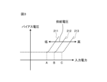
- FIG. 3 is a diagram showing the relationship among the bias voltage, input power, and supply voltage of the control circuit of the first embodiment.
- FIG. 4 is a diagram showing the configuration of a Doherty amplifier circuit according to the second embodiment.
- FIG. 5 is a diagram showing the configuration of an amplification system according to the third embodiment.
- FIG. 6 is a diagram showing the configuration of a Doherty amplifier circuit according to a fourth embodiment.
- FIG. 7 is a diagram showing the configuration of a control circuit according to the fifth embodiment.
- FIG. 1 is a diagram showing the configuration of a Doherty amplifier circuit according to a first embodiment.
- FIG. 2 is a diagram showing the relationship between bias voltage, input power, and supply voltage in a comparative example.
- FIG. 3 is a
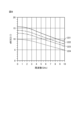
- FIG. 8 is a diagram showing the pass characteristic of the first variable pass characteristic circuit of the control circuit according to the fifth embodiment.
- FIG. 9 is a diagram showing the configuration of a control circuit according to the sixth embodiment.
- FIG. 10 is a diagram showing the configuration of a control circuit according to the seventh embodiment.
- FIG. 11 is a diagram showing a circuit example of a variable current source circuit.
- FIG. 1 is a diagram showing the configuration of a Doherty amplifier circuit according to a first embodiment.
- the Doherty amplifier circuit 1 amplifies a high frequency input signal RFin input to an input terminal 1a, and outputs a high frequency output signal RFout from an output terminal 1b.
- the Doherty amplifier circuit 1 includes a bias circuit 10, a carrier amplifier 11, a peak amplifier 12, a divider 13, a coupler 14, a detector 15, and a control circuit 16.
- Bias circuit 10 outputs bias voltage V BIAS1 to carrier amplifier 11.
- the carrier amplifier 11 outputs a high frequency signal RF1 obtained by amplifying the high frequency input signal RFin to the coupler 14.
- the divider 13 outputs a high frequency signal RF2 having a phase difference of approximately 90° from the high frequency input signal RFin to the peak amplifier 12. Note that “approximately 90°” includes not only a phase of 90° but also a phase of 90° ⁇ 45°. Although the divider 13 is exemplified as a 90° hybrid circuit, the present disclosure is not limited thereto.
- the peak amplifier 12 outputs a high frequency signal RF3 obtained by amplifying the high frequency signal RF2.
- the coupler 14 outputs a high frequency output signal RFout, which is a combination of the high frequency signal RF1 and the high frequency signal RF3, from the output terminal 1b of the Doherty amplifier circuit 1.
- the detector 15 detects the high frequency input signal RFin and outputs a high frequency signal RF4 corresponding to the high frequency input signal RFin to the control circuit 16.
- a supply voltage Vcc supplied to the final stage amplifier is input to the input terminal 1c of the Doherty amplifier circuit 1.
- the final stage amplifiers are, for example, the carrier amplifier 11 and the peak amplifier 12 when there is no amplifier at the subsequent stage of the Doherty amplifier circuit 1. Further, for example, if there is an amplifier at the subsequent stage of the Doherty amplifier circuit 1, the final stage amplifier is the amplifier.
- the supply voltage Vcc input to the input terminal 1c of the Doherty amplifier circuit 1 is supplied to one of the one or more amplifiers when there is one or more amplifiers in the preceding stage of the Doherty amplifier circuit 1. It may be the supply voltage Vcc. Furthermore, even in the case where there is one or more amplifiers after the Doherty amplifier circuit 1, the supply voltage Vcc may be supplied to the carrier amplifier 11 and the peak amplifier 12.
- the supply voltage Vcc is, for example, a power supply voltage that changes according to the envelope of the high-frequency input signal RFin, that is, is envelope tracking controlled, but the present disclosure is not limited thereto.
- Control circuit 16 outputs bias voltage V BIAS2 to peak amplifier 12 based on high frequency signal RF4 and supply voltage Vcc.
- FIG. 2 is a diagram showing the relationship between bias voltage, input power, and supply voltage in a comparative example.
- the vertical axis represents the bias voltage V BIAS2
- the horizontal axis represents the input power of the high frequency input signal RFin.
- the comparative example outputs the bias voltage V BIAS2 based only on the supply voltage Vcc without depending on the input power.
- Line 201 represents the bias voltage V BIAS2 when the supply voltage Vcc is relatively low.
- Line 202 represents the bias voltage V BIAS2 when the supply voltage Vcc is relatively intermediate.
- Line 203 represents the bias voltage V BIAS2 when the supply voltage Vcc is relatively high.
- FIG. 3 is a diagram showing the relationship among the bias voltage, input power, and supply voltage of the control circuit of the first embodiment.
- the vertical axis represents the bias voltage V BIAS2
- the horizontal axis represents the input power of the high frequency input signal RFin.
- the control circuit 16 of the first embodiment outputs the bias voltage V BIAS2 based on the input power and the supply voltage Vcc.
- Line 211 represents the bias voltage V BIAS2 when the supply voltage Vcc is relatively low.
- Line 212 represents the bias voltage V BIAS2 when the supply voltage Vcc is relatively intermediate.
- Line 213 represents the bias voltage V BIAS2 when the supply voltage Vcc is relatively high.
- the control circuit 16 operates (starts up) the peak amplifier 12 more by increasing the bias voltage V BIAS2 as the supply voltage Vcc is lower. Conversely, the higher the supply voltage Vcc, the more difficult it is for the carrier amplifier 11 to saturate. Therefore, the control circuit 16 suppresses (stops) the operation of the peak amplifier 12 by lowering the bias voltage V BIAS2 as the supply voltage Vcc is higher.
- the control circuit 16 operates (starts up) the peak amplifier 12 more by increasing the bias voltage V BIAS2 as the input power increases. Conversely, the smaller the input power, the more difficult it is for the carrier amplifier 11 to saturate. Therefore, the control circuit 16 suppresses (stops) the operation of the peak amplifier 12 by lowering the bias voltage V BIAS2 as the input power is smaller.
- the input power threshold when the supply voltage Vcc is relatively low (line 211) is set to threshold A
- the input power threshold when the supply voltage Vcc is relatively intermediate (line 212) is set to threshold B
- Let the input power threshold value when the supply voltage Vcc is relatively high (line 213) be the threshold value C.
- a ⁇ B ⁇ C the control circuit 16 keeps the bias voltage V BIAS2 constant when the input power is less than the threshold value, and increases the bias voltage V BIAS2 as the input power increases when the input power is equal to or higher than the threshold value.
- the Doherty amplifier circuit 1 of the first embodiment can suppress power consumption by suppressing unnecessary operations of the peak amplifier 12 when the supply voltage Vcc suddenly increases.
- Supply voltage Vcc is generally determined by input power in many cases. That is, the larger the input power, the higher the supply voltage Vcc, and the smaller the input power, the lower the supply voltage Vcc. However, due to the effects of temperature changes, disturbance noise, etc., the supply voltage Vcc may momentarily increase even though the input power is small.
- Non-Patent Document 1 and the comparative example attempt to operate so as to lower the bias point of the peak amplifier 12.
- a delay caused by a delay (time constant) of the control circuit a state where the supply voltage Vcc is high and the bias voltage V BIAS2 is high instantaneously occurs.
- a high supply voltage Vcc is input to the peak amplifier 12, and a large bias current flows, resulting in a large amount of power being wasted.
- the Doherty amplifier circuit 1 As shown by lines 211 to 213 in FIG. 3, when the input power is small, the bias voltage V BIAS2 becomes low and the peak amplifier 12 is stopped. Therefore, the Doherty amplifier circuit 1 can suppress wasteful power consumption as in Non-Patent Document 1 and the comparative example.
- the Doherty amplifier circuit 1 of the first embodiment can suppress the start-up delay of the peak amplifier 12 and suppress the occurrence of distortion in the high-frequency output signal RFout when the supply voltage Vcc suddenly drops.
- the supply voltage Vcc may drop instantaneously due to the influence of temperature changes, disturbance noise, etc.
- the Doherty amplifier circuit 1 when the Doherty amplifier circuit 1 is mounted on a vehicle, an instantaneous low voltage that occurs when another device connected to the same power supply system consumes a large current when the engine is started is exemplified.
- Non-Patent Document 1 and the comparative example attempt to operate to raise the bias point of the peak amplifier 12.
- a state where the supply voltage Vcc is low and the bias voltage V BIAS2 is low instantaneously occurs.
- the peak amplifier 12 is not activated, the peak amplifier 12 does not amplify the high frequency signal RF2, and large distortion occurs in the high frequency output signal RFout.
- the Doherty amplifier circuit 1 when the input power is large, the bias voltage V BIAS2 becomes high regardless of the supply voltage Vcc, and the peak amplifier 12 is activated. . Therefore, the Doherty amplifier circuit 1 can suppress the occurrence of distortion in the high frequency output signal RFout.
- FIG. 4 is a diagram showing the configuration of a Doherty amplifier circuit according to the second embodiment.
- the Doherty amplifier circuit 1A includes a control circuit 16A instead of the control circuit 16.
- the control circuit 16A includes a first variable pass characteristic circuit 21, a detector 22, and a bias circuit 23.
- the threshold value of the pass characteristic changes depending on the supply voltage Vcc, and the pass characteristic that allows the high frequency signal RF4 to pass changes.
- the first variable pass characteristic circuit 21 has a high pass characteristic when the supply voltage Vcc is relatively low.
- the first variable pass characteristic circuit 21 has a low pass characteristic when the supply voltage Vcc is relatively high.
- the first passage characteristic variable circuit 21 controls the amount of passage (degree of passage) of the high frequency signal RF4 according to the passage characteristic, and outputs the high frequency signal RF5 to the detector 22.
- the high frequency signal RF5 has power that corresponds to both the supply voltage Vcc and the input power of the high frequency input signal RFin.
- the detector 22 detects (or rectifies) the high frequency signal RF5 and outputs a signal S1 corresponding to the high frequency signal RF5 to the bias circuit 23.
- the bias circuit 23 outputs a bias voltage V BIAS2 according to the signal S1 to the peak amplifier 12.
- the control circuit 16A can suitably control the bias point of the peak amplifier 12 by supplementarily using the supply voltage Vcc.
- the Doherty amplifier circuit 1A can suppress power consumption and suppress the occurrence of distortion in the high-frequency output signal RFout even if the supply voltage Vcc fluctuates due to the influence of disturbance noise or the like.
- the detector 22 is a single-end detector, but the present disclosure is not limited thereto.
- the detector 22 may be a differential detector.
- a balun for converting the high frequency signal RF5 into a differential high frequency signal is provided between the first variable pass characteristic circuit 21 and the detector 22, and the detector 22 converts the differential high frequency signal output from the balun into a differential high frequency signal. It is also possible to perform wave detection.
- the supply voltage Vcc is often managed by the system controlling the Doherty amplifier circuit 1A.
- a method may be adopted in which the pass characteristic of the first variable pass characteristic circuit 21 is digitally controlled according to the supply voltage Vcc managed by the system.
- controlling the pass characteristic of the first variable pass characteristic circuit 21 in an analog manner according to the supply voltage Vcc is more effective in dealing with fluctuations in the supply voltage Vcc that cannot be managed by the system, such as the above-mentioned disturbance noise. It becomes like this.
- the pass characteristic of the first variable pass characteristic circuit 21 may be processed by analog processing, digital processing, or a combination of analog processing and digital processing.
- FIG. 5 is a diagram showing the configuration of an amplification system according to the third embodiment.
- the amplification system 31 includes a Doherty amplification circuit 1B, a digital system 32, and a voltage supply circuit 33.
- the Doherty amplifier circuit 1B includes a control circuit 16B instead of the control circuit 16A.
- the control circuit 16B includes a first variable pass characteristic circuit 21B instead of the first variable pass characteristic circuit 21.
- the digital system 32 controls the entire Doherty amplifier circuit 1B.
- the digital system 32 is exemplified by an envelope tracking circuit, the present disclosure is not limited thereto.
- the digital system 32 outputs a signal S11 indicating the supply voltage Vcc to the voltage supply circuit 33.
- the digital system 32 is an envelope tracking circuit, it changes the signal S11 according to the envelope of the high frequency input signal RFin.
- the signal S11 may be a digital signal or an analog signal.
- the voltage supply circuit 33 outputs a supply voltage Vcc according to the signal S11 to the carrier amplifier 11 and the peak amplifier 12.
- the carrier amplifier 11 and the peak amplifier 12 operate using the supply voltage Vcc as a power supply voltage.
- the digital system 32 outputs a signal S12 corresponding to the supply voltage Vcc to the first variable pass characteristic circuit 21B via the input terminal 1c.
- the digital system 32 is an envelope tracking circuit, it changes the signal S12 according to the envelope of the high frequency input signal RFin.
- the signal S12 may be a digital signal or an analog signal.
- the first passage characteristic variable circuit 21B changes its passage characteristic in accordance with the signal S12. In other words, the first variable pass characteristic circuit 21B changes its pass characteristic according to the supply voltage Vcc.
- the first variable passage characteristic circuit 21B controls the amount of passage (degree of passage) of the high frequency signal RF4 according to the passage characteristic, and outputs the high frequency signal RF5 to the detector 22.
- the high frequency signal RF5 has power that corresponds to both the supply voltage Vcc and the input power of the high frequency input signal RFin.
- the Doherty amplifier circuit 1B can control the bias voltage V BIAS2 of the peak amplifier 12 according to the signal S12 input from the digital system 32. As a result, the signal S12 does not pass through the voltage supply circuit 33 in the Doherty amplifier circuit 1B, compared to the case where the supply voltage Vcc itself is input (see FIG. 4), so that delays in the control circuit 16B can be suppressed. Can be done.
- the Doherty amplifier circuit of the present disclosure has good compatibility with other peak amplifier control techniques.
- the Doherty amplifier circuit of the present disclosure controls activation of the peak amplifier based on the drive level (saturation degree) of an amplifier other than the peak amplifier (for example, a carrier amplifier, an amplifier at the subsequent stage of the Doherty amplifier circuit 1) and input power.
- an amplifier other than the peak amplifier for example, a carrier amplifier, an amplifier at the subsequent stage of the Doherty amplifier circuit 1
- input power for example, a carrier amplifier, an amplifier at the subsequent stage of the Doherty amplifier circuit
- FIG. 6 is a diagram showing the configuration of a Doherty amplifier circuit according to the fourth embodiment.
- the Doherty amplifier circuit 1C includes a control circuit 16C instead of the control circuit 16A. Compared to the control circuit 16A, the control circuit 16C further includes a second variable pass characteristic circuit 24.
- a signal S21 representing the drive level of the carrier amplifier 11 is input from the bias circuit 10 to the second variable pass characteristic circuit 24.
- the signal S21 may be a signal (inverted signal) that changes complementary to the drive level of the carrier amplifier 11.
- the Doherty amplifier circuit 1C outputs the signal S22 representing the drive level of the carrier amplifier 11 to the second pass characteristic variable circuit 24 based on the detector 17 that detects the high frequency signal RF1 and the detection signal of the detector 17.
- a drive level detector 18 may also be included.
- the signal S22 may be a signal (inverted signal) that changes complementary to the drive level of the carrier amplifier 11.
- At least one of the signal S21 and the signal S22 may be input to the second variable pass characteristic circuit 24.
- a signal in which the signal S21 and the signal S22 are combined into one signal may be input to the second variable pass characteristic circuit 24.
- a signal representing the drive level of the carrier amplifier 11 is input to the control circuit 16C, but the present disclosure is not limited thereto. It is only necessary that a signal representing the drive level of an amplifier other than the peak amplifier 12 is input to the control circuit 16C. For example, a signal representing the drive level of an amplifier downstream of the Doherty amplifier circuit 1C may be input to the control circuit 16C.
- the second pass characteristic variable circuit 24 changes its pass characteristic according to the drive level of the carrier amplifier 11.
- the second variable pass characteristic circuit 24 has a low pass characteristic when the drive level of the carrier amplifier 11 is relatively low.
- the second variable pass characteristic circuit 24 has a high pass characteristic when the drive level of the carrier amplifier 11 is relatively high.
- the second passage characteristic variable circuit 24 controls the amount of passage (degree of passage) of the high frequency signal RF5 according to the passage characteristic, and outputs the high frequency signal RF6 to the detector 22.
- the high frequency signal RF6 has power according to the supply voltage Vcc, the input power of the high frequency input signal RFin, and the drive level of the carrier amplifier 11.
- the Doherty amplifier circuit 1C can suitably control the bias point of the peak amplifier 12 by supplementarily using the supply voltage Vcc.
- the Doherty amplifier circuit 1C can suppress power consumption and suppress the occurrence of distortion in the high-frequency output signal RFout even if the supply voltage Vcc fluctuates due to the influence of disturbance noise or the like.
- the carrier amplifier 11 becomes saturated even if the power of the high-frequency input signal RFin is small. It is possible.
- the second pass characteristic variable circuit 24 detects the drive level of the carrier amplifier 11, and when the carrier amplifier 11 is close to saturation, it detects the drive level of the carrier amplifier 11 even if the power of the high frequency signal RF4 is small. , the peak amplifier 12 is started immediately.
- the control circuit 16C Since the first variable pass characteristic circuit 21 detects the high frequency signal RF4, even if it takes time for the second variable pass characteristic circuit 24 to detect the drive level of the carrier amplifier 11, the control circuit 16C The peak amplifier 12 can be activated without saturating the peak amplifier 12. Thereby, the Doherty amplifier circuit 1C can suppress distortion of the high frequency output signal RFout.
- control circuit 16C operates in a feedforward manner in response to the high frequency input signal RFin, and operates in a feedback manner in response to at least one of the signal S21 and the signal S22.
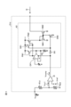
- FIG. 7 is a diagram showing the configuration of a control circuit according to the fifth embodiment.
- the control circuit 16D includes a first variable pass characteristic circuit 21 and a detector 22.
- the bias circuit 23 can be omitted because the detector 22 has a high current supply capability. That is, in the control circuit 16D, the detector 22 also has the function of the bias circuit 23.
- the first variable pass characteristic circuit 21 includes a pull-out section 21a, a bias section 21b, and a signal passing section 21c.
- the extraction section 21a extracts the current I2 from the bias section 21b according to the supply voltage Vcc.
- the extractor 21a is a circuit that converts an increase or decrease in the supply voltage Vcc into an increase or decrease in the current I2.
- the bias section 21b is a circuit that outputs a bias current I4 to the signal passing section 21c according to the current I2.
- the signal passing section 21c is a circuit that amplifies the high frequency signal RF4 and outputs the high frequency signal RF5 according to the bias current I4.
- the extracted portion 21a includes resistors R1 and R2, and transistors Q1, Q2, Q3, and Q4.
- each transistor is a bipolar transistor, but the present disclosure is not limited thereto.
- An example of the bipolar transistor is a heterojunction bipolar transistor (HBT), but the present disclosure is not limited thereto.
- the transistor may be, for example, a field effect transistor (FET).
- FET field effect transistor
- the transistor may be a multi-finger transistor in which a plurality of unit transistors are electrically connected in parallel.
- a unit transistor refers to the minimum configuration of a transistor.
- each transistor is a FET
- the drain of the FET corresponds to the collector of the bipolar transistor
- the gate of the FET corresponds to the base of the bipolar transistor
- the source of the FET corresponds to the emitter of the bipolar transistor.
- a supply voltage Vcc is input to one end of the resistor R1.
- the other end of the resistor R1 is electrically connected to the collector of the transistor Q1.
- the base of transistor Q1 is electrically connected to node N1.
- the emitter of transistor Q1 is electrically connected to node N2.
- a set constant current I1 is input from the current source 51 to one end of the resistor R2.
- the other end of the resistor R2 is electrically connected to the node N1.
- the collector and base of transistor Q2 are electrically connected to node N1. That is, the transistor Q1 and the transistor Q2 are connected in a current mirror.
- the emitter of transistor Q2 is electrically connected to node N2.
- the collector and base of transistor Q3 are electrically connected to node N2.
- the emitter of transistor Q3 is electrically connected to a reference potential.
- transistor Q4 The base of transistor Q4 is electrically connected to node N2. In other words, transistor Q3 and transistor Q4 are connected in a current mirror manner. The emitter of transistor Q4 is electrically connected to a reference potential. The collector of transistor Q4 is electrically connected to node N4 of bias section 21b.
- the current I2 flowing from the node N4 to the collector of the transistor Q4 is the output current of the extraction portion 21a.
- the bias section 21b includes transistors Q5, Q6, and Q7.
- transistor Q5 The collector and base of transistor Q5 are electrically connected to node N3. That is, transistor Q5 is diode-connected. A set constant current I3 is input from the current source 52 to the node N3. The emitter of transistor Q5 is electrically connected to node N4.
- transistor Q6 The collector and base of transistor Q6 are electrically connected to node N4. That is, transistor Q6 is diode-connected.
- the emitter of transistor Q6 is electrically connected to a reference potential.
- a power supply voltage is input to the collector of the transistor Q7.
- the base of transistor Q7 is electrically connected to node N3.
- transistor Q5 and transistor Q7 are connected in a current mirror.
- the emitter of the transistor Q7 is electrically connected to one end of the resistor R3 of the signal passing section 21c. In other words, the transistor Q7 and the resistor R3 are connected in an emitter follower manner.
- the emitter current of transistor Q7 is bias current I4.
- the signal passing section 21c includes resistors R3 and R4, a capacitor C1, and a transistor Q8.
- the other end of the resistor R3 is electrically connected to the base of the transistor Q8. Bias current I4 flowing into one end of resistor R3 is input to the base of transistor Q8.
- a high frequency signal RF4 is input to one end of the capacitor C1.
- the other end of capacitor C1 is electrically connected to the base of transistor Q8.
- the capacitor C1 is a DC cut capacitor that cuts the DC component of the high frequency signal RF4.
- a power supply voltage is input to one end of the resistor R4.
- the other end of resistor R4 is electrically connected to the collector of transistor Q8.
- the emitter of transistor Q8 is electrically connected to the reference potential.
- the signal passing section 21c amplifies the high frequency signal RF4 according to the bias current I4, and outputs the high frequency signal RF5 from the collector.
- the voltage at the node N1 of the extraction portion 21a is approximately 2V BE , where VBE is the base-emitter voltage of each transistor.
- the constant current I1 flows to the supply voltage Vcc side via the PN junction between the base and collector of the transistor Q1. Therefore, no current flows into node N2. Therefore, current I2 does not flow between the collector and emitter of transistor Q4.
- the bias section 21b outputs a relatively large bias current I4 to the base of the transistor Q8 of the signal passing section 21c.
- the transistor Q8 When the relatively large bias current I4 is input to the base of the transistor Q8, the transistor Q8 outputs a high frequency signal RF5 with relatively large power.
- the first variable pass characteristic circuit 21 relatively increases the power of the high frequency signal RF5 when the supply voltage Vcc is a relatively low voltage.
- transistor Q1 gradually begins to operate properly, and transistor Q1 and transistor Q2 perform a current mirror operation.
- the constant current I1 flows into the node N2 via the collector (base) and emitter of the transistor Q2. Further, as the transistor Q1 and the transistor Q2 perform a current mirror operation, the emitter current of the transistor Q1 proportional to the emitter current of the transistor Q2 flows into the node N2. The current flowing into node N2 flows between the collector (base) and emitter of transistor Q3.
- Transistor Q3 and transistor Q4 are connected in a current mirror manner. Therefore, a current I2 proportional to the current flowing into node N2 flows between the collector and emitter of transistor Q4.
- the transistor Q8 When the relatively small bias current I4 is input to the base of the transistor Q8, the transistor Q8 outputs a high frequency signal RF5 with relatively small power.
- the high frequency signal RF5 output from the first variable pass characteristic circuit 21 is input to the detector 22 via the DC cut capacitor 101.
- FIG. 8 is a diagram showing the pass characteristic of the first variable pass characteristic circuit of the control circuit according to the fifth embodiment.
- the vertical axis represents the S parameter (S(2,1)) of the first variable pass characteristic circuit 21, and the horizontal axis represents the frequency.
- the detector 22 includes a bias section 22a, a detection section 22b, and a filter section 22c.
- the bias section 22a includes transistors Q11, Q12, and Q13.
- the collector and base of the transistor Q11 are electrically connected to the node N11.
- transistor Q11 is diode-connected.
- a set constant current I11 is input from the current source 53 to the node N11.
- transistor Q12 The collector and base of transistor Q12 are electrically connected to the emitter of transistor Q11. That is, transistor Q12 is diode-connected. The emitter of transistor Q12 is electrically connected to a reference potential.
- the voltage at the node N11 is approximately 2V BE .
- the base of transistor Q13 is electrically connected to the collector and base of transistor Q12. In other words, the transistor Q12 and the transistor Q13 are connected in a current mirror.
- the emitter of transistor Q13 is electrically connected to a reference potential.
- the detection section 22b includes a resistor R11 and a transistor Q14.
- resistor R11 One end of the resistor R11 is electrically connected to the node N11. The other end of resistor R11 is electrically connected to the base of transistor Q14.
- the base bias voltage of transistor Q14 is determined by the voltage at node N11.
- a power supply voltage is input to the collector of the transistor Q14.
- the high frequency signal RF5 after passing through the DC cut capacitor 101 is input to the base of the transistor Q14.
- the emitter of transistor Q14 is electrically connected to the collector of transistor Q13.
- transistor Q14 Of the emitter current of transistor Q14, a certain amount of current flows between the collector and emitter of transistor Q13, and the remaining current flows to filter section 22c.
- the filter section 22c includes an inductor L11 and a capacitor C11.
- the filter section 22c is a low-pass filter that removes the fundamental wave component of the high frequency signal RF5. Note that if the detector 22 is a differential detector, the filter section 22c can be omitted.
- inductor L11 One end of inductor L11 is electrically connected to the emitter of transistor Q14. The other end of the inductor L11 is electrically connected to one end of the capacitor C11. The other end of the capacitor C11 is electrically connected to a reference potential. The voltage of the capacitor C11 becomes the bias voltage VBIAS2 of the peak amplifier 12.
- the transistor Q14 is turned on when the high frequency signal RF5 is equal to or higher than the threshold voltage of the transistor Q14, and outputs an emitter current.
- transistor Q14 Of the emitter current of transistor Q14, a certain amount of current flows between the collector and emitter of transistor Q13, and the remaining current flows to filter section 22c.
- the control circuit 16D can implement a circuit that appropriately controls the bias point of the peak amplifier 12 by using the supply voltage Vcc auxiliary.
- the control circuit 16C can realize a circuit that can suppress power consumption and suppress generation of distortion in the high-frequency output signal RFout even if the supply voltage Vcc fluctuates due to the influence of disturbance noise or the like.
- FIG. 9 is a diagram showing the configuration of a control circuit according to the sixth embodiment.
- control circuit 16E Compared to the control circuit 16D (see FIG. 7), the control circuit 16E further includes a second variable pass characteristic circuit 24.
- the second variable passage characteristic circuit 24 includes a signal passage section 24a and a current source 24b.
- the signal passing section 24a includes a transistor Q21.
- a power supply voltage is input to the collector of the transistor Q21.
- a high frequency signal RF5 is input to the base of the transistor Q21.
- the emitter of transistor Q21 is electrically connected to current source 24b.
- the current source 24b draws a current from the emitter of the transistor Q21 according to at least one of the signal S21 and the signal S22 representing the drive level of the carrier amplifier 11.
- the current source 24b draws a large current from the emitter of the transistor Q21 when the carrier amplifier 11 is saturated. Thereby, transistor Q21 operates as an emitter follower circuit and maintains high pass characteristics.
- the current source 24b does not apply an appropriate bias to the emitter of the transistor Q21 when the carrier amplifier 11 is out of saturation.
- the transistor Q21 has a low pass characteristic.
- the carrier amplifier 11 is unlikely to become saturated when the temperature or other surrounding environment changes (for example, when the gain of the carrier amplifier 11 increases at an extremely low temperature) even if the power of the high-frequency input signal RFin is small. could be.
- the control circuit 16E detects the drive level of the carrier amplifier 11, and when the carrier amplifier 11 is close to saturation, the control circuit 16E immediately switches to the peak amplifier even if the power of the high frequency signal RF4 is small. 12 can be realized.
- FIG. 10 is a diagram showing the configuration of a control circuit according to the seventh embodiment.
- the control circuit 16F differs from the control circuit 16D (see FIG. 7) in part in the configuration of the first variable pass characteristic circuit 21. Specifically, in the control circuit 16F, the first variable pass characteristic circuit 21F includes a drawing section 21d instead of the current source 51 and the drawing section 21a, compared to the first variable passing characteristic circuit 21.
- the extraction section 21d includes resistors R1d and R2d, a comparator 61, and a variable current source circuit 62.
- a supply voltage Vcc is input to one end of the resistor R1d.
- the other end of the resistor R1d is electrically connected to one end of the resistor R2d.
- the other end of the resistor R2d is electrically connected to a reference potential.
- the comparator 61 includes a first input terminal, a second input terminal, and an output terminal. A connection point between the other end of the resistor R1d and one end of the resistor R2d is electrically connected to the first input terminal of the comparator 61, and a voltage Vcc1 obtained by dividing the supply voltage Vcc by the resistor R1d and the resistor R2d is applied. be done. A reference voltage Vref is applied to the second input terminal of the comparator 61. The comparator 61 compares the voltage Vcc1 applied to the first input terminal with the reference voltage Vref applied to the second input terminal, and outputs a comparison result output signal Vcomp indicating the comparison result from the output terminal.
- the variable current source circuit 62 is electrically connected to the output terminal of the comparator 61.
- the variable current source circuit 62 draws the current I2 from the bias section 21b in accordance with the comparison result output signal Vcomp output from the output terminal of the comparator 61.
- the variable current source circuit 62 converts an increase or decrease in the supply voltage Vcc into an increase or decrease in the current I2, and draws the current I2 from the bias section 21b according to the supply voltage Vcc.
- the comparator 61 outputs a Low level signal as the comparison result output signal Vcomp.
- the variable current source circuit 62 is not driven and is in an off state. Therefore, current I2 does not flow.
- the bias section 21b outputs a relatively large bias current I4 to the base of the transistor Q8 of the signal passing section 21c.
- the transistor Q8 When the relatively large bias current I4 is input to the base of the transistor Q8, the transistor Q8 outputs a high frequency signal RF5 with relatively large power.
- the first variable pass characteristic circuit 21F relatively increases the power of the high frequency signal RF5 when the supply voltage Vcc is relatively low.
- the comparator 61 outputs a High level signal as the comparison result output signal Vcomp.
- the variable current source circuit 62 starts driving and becomes on state. Therefore, a current I2 proportional to the magnitude of the comparison result output signal Vcomp begins to flow.
- the bias section 21b outputs a relatively small bias current I4 to the base of the transistor Q8 of the signal passing section 21c.
- the transistor Q8 When the relatively small bias current I4 is input to the base of the transistor Q8, the transistor Q8 outputs a high frequency signal RF5 with relatively small power.
- the first variable pass characteristic circuit 21F relatively increases the power of the high frequency signal RF5 when the supply voltage Vcc increases and becomes a relatively high voltage.
- control circuit 16F may be configured to include a plurality of semiconductor dies. Specifically, in the control circuit 16F, the extraction portion 21d and the current source 52 included in the first variable pass characteristic circuit 21F are formed on a first semiconductor die having a semiconductor substrate made of silicon (Si), for example. is exemplified. Further, the remaining portions of the control circuit 16F except for the extraction portion 21d and the current source 52 are exemplified as being formed on a second semiconductor die having a semiconductor substrate made of gallium arsenide (GaAs), for example. In addition to the extraction section 21d of the control circuit 16F and the current source 52, another control circuit for controlling the carrier amplifier 11 and the peak amplifier 12 may be formed in the first semiconductor die. Moreover, in addition to the remaining portions of the control circuit 16F, the carrier amplifier 11 and the peak amplifier 12 may be formed in the second semiconductor die.
- Si silicon
- GaAs gallium arsenide
- variable current source circuit 62 a circuit example of the variable current source circuit 62 will be explained.
- FIG. 11 is a diagram showing a circuit example of the variable current source circuit 62.
- the variable current source circuit 62 includes, for example, an operational amplifier OP1, an inverter IN1, PMOS transistors PM1, PM2, switches SW1, SW2, NMOS transistors NM1, NM2, and a resistor R3.
- the operational amplifier OP1 has a non-inverting input terminal, an inverting input terminal, and an output terminal.
- a non-inverting input terminal of the operational amplifier OP1 is connected to a reference potential.
- the inverting input terminal of the operational amplifier OP1 is connected to one end of the resistor R3 and the output terminal of the operational amplifier OP1. The other end of resistor R3 is grounded.
- the source terminal of the PMOS transistor PM1 is connected to a fixed potential (eg, power supply potential).
- the drain terminal of the PMOS transistor PM1 is connected to the output terminal of the operational amplifier OP1.
- the gate of the PMOS transistor PM1 is connected to the gate of the PMOS transistor PM2 and one end of the switch SW1.
- the source terminal of the PMOS transistor PM2 is connected to a fixed potential (eg, power supply potential).
- the drain terminal of the PMOS transistor PM2 is connected to the drain of the NMOS transistor PM1.
- the gate of the PMOS transistor PM2 is connected to the gate of the PMOS transistor PM1 and one end of the switch SW1.
- One end of the switch SW1 is connected to the gates of the PMOS transistors PM1 and PM2, and the other end is connected to a fixed potential (eg, power supply potential).
- the drain of the NMOS transistor NM1 is connected to the gate, and the source is grounded. Further, the NMOS transistor NM2 has a drain connected to the bias section 21b, a gate connected to the gate of the NMOS transistor NM1, and a source grounded. In other words, the NMOS transistors NM1 and NM2 constitute a current mirror circuit. The gate of the NMOS transistor NM1 and the gate of the NMOS transistor NM2 are grounded via a switch SW2.
- a comparison result output signal Vcomp output from the output terminal of the comparator 61 is input to the operational amplifier OP1 as a control signal. Furthermore, a comparison result output signal Vcomp outputted from the output terminal of the comparator 61 is input to each of the switches SW1 and SW2 as a control signal via an inverter IN1.
- the operational amplifier OP1 to which the low level signal is input as a control signal is turned off. Furthermore, the switches SW1 and SW2, to which a High level signal obtained by inverting the Low bell signal is inputted as a control signal, are both in a closed state. In this case, the switch SW1 brings the gate potential and source potential of the PMOS transistors PM1 and PM2 to the same potential. Furthermore, the gate of the NMOS transistor NM1 and the gate of the NMOS transistor NM2 are fixed to the ground potential by the switch SW2. Therefore, variable current source circuit 62 is turned off.
- the operational amplifier OP1 to which the high level signal is input as a control signal is turned on.
- the switches SW1 and SW2, to which a low level signal obtained by inverting the high level signal is inputted as a control signal are both in an open state.
- the gate potential and source potential of the PMOS transistors PM1 and PM2 are set to different potentials by the switch SW1.
- the gate of the NMOS transistor NM1 and the gate of the NMOS transistor NM2 are not fixed to the ground potential by the switch SW2. Therefore, the variable current source circuit 62 is turned on.
- the present disclosure can also have the following configuration.
- a carrier amplifier that amplifies high frequency signals, a peak amplifier that amplifies the high frequency signal; a first variable pass characteristic circuit whose pass characteristic for passing the high frequency signal is variable in accordance with a supply voltage; and a detector that detects the high frequency signal after passing through the first variable pass characteristic circuit; a control circuit that controls the bias of the peak amplifier according to the detection result of the wave detector; including, Doherty amplifier circuit.
- the control circuit includes: a second variable pass characteristic electrically connected between the first variable pass characteristic circuit and the detector, the pass characteristic for passing the high frequency signal being variable in accordance with the drive level of an amplifier other than the peak amplifier; further comprising a circuit; Doherty amplifier circuit.
- the Doherty amplifier circuit according to (1) or (2) above, The first variable pass characteristic circuit is a passage section that allows the high-frequency signal to pass; a bias section that controls the bias of the passage section; a drawing part that draws current from the bias part according to the supply voltage; including, Doherty amplifier circuit.
- the pull-out part is a first transistor having a collector or drain to which the supply voltage is input, a base or gate electrically connected to a first node into which a constant current flows, and an emitter or source electrically connected to a second node; a second transistor whose collector or drain and base or gate are electrically connected to the first node, and whose emitter or source is electrically connected to the second node; a third transistor whose collector or drain and base or gate are electrically connected to the second node, and whose emitter or source is electrically connected to a reference potential; a fourth transistor whose base or gate is electrically connected to the second node, whose emitter or source is electrically connected to a reference potential, and which draws current from the bias section to the collector; including, Doherty amplifier circuit.
- the Doherty amplifier circuit according to any one of (1) to (4) above,
- the supply voltage is a power supply voltage supplied to the final stage amplifier, or a voltage corresponding to the power supply voltage, Doherty amplifier circuit.
- a carrier amplifier that amplifies high frequency signals a peak amplifier that amplifies the high frequency signal; a control circuit that controls the bias of the peak amplifier; including;
- the control circuit includes: A first pass characteristic for passing the high frequency signal is variable, a threshold value of the pass characteristic changes depending on the supply voltage, and the first pass characteristic is relatively low as the supply voltage is relatively high.
- a variable pass characteristic circuit a detector that detects the high frequency signal after passing through the first variable pass characteristic circuit; including; controlling the bias of the peak amplifier according to the detection result of the wave detector; Doherty amplifier circuit.
- the Doherty amplifier circuit includes: A second pass characteristic that is electrically connected between the first variable pass characteristic circuit and the detector and that allows the high frequency signal to pass through is variable, and the drive level of the amplifiers other than the peak amplifier is relatively high. further comprising a second pass characteristic variable circuit in which the second pass characteristic is relatively high; Doherty amplifier circuit.
- a carrier amplifier that amplifies high frequency signals, a peak amplifier that amplifies the high frequency signal; a control circuit that controls the bias of the peak amplifier; including; The control circuit controls a bias of the peak amplifier according to a supply voltage and the high frequency signal.
- Doherty amplifier circuit Doherty amplifier circuit.
- the control circuit further controls a bias of the peak amplifier according to a drive level of an amplifier other than the peak amplifier. Doherty amplifier circuit.
- the Doherty amplifier circuit according to (8) or (9) above, The control circuit includes: a first variable pass characteristic circuit whose pass characteristic for passing the high frequency signal is variable according to the supply voltage; and a detector that detects the high frequency signal after passing through the first variable pass characteristic circuit. Doherty amplifier circuit.
- the Doherty amplifier circuit according to (3) above, The pull-out part is a first resistance element to which the supply voltage is input; a second resistance element, one end of which is electrically connected to the other end of the first resistance element, and the other end of which is electrically connected to a reference potential; It has a first input terminal, a second input terminal, and an output terminal, and the first input terminal receives a signal output from a connection point between the other end of the first resistance element and one end of the second resistance element.
- a comparator that receives a reference voltage input to the second input terminal and outputs a comparison result output signal from the output terminal; a variable current source circuit that changes the current drawn from the bias section according to the comparison result output signal output from the output terminal of the comparator; including, Doherty amplifier circuit.
- the extraction section is formed on a first semiconductor die, and the passage section and the bias section are formed on a second semiconductor die, The material of the first semiconductor substrate included in the first semiconductor die is different from the material of the second semiconductor substrate included in the second semiconductor die, Doherty amplifier circuit.
Landscapes
- Engineering & Computer Science (AREA)
- Power Engineering (AREA)
- Microelectronics & Electronic Packaging (AREA)
- Amplifiers (AREA)
Abstract
Description
(構成)
図1は、第1の実施の形態のドハティ増幅回路の構成を示す図である。ドハティ増幅回路1は、入力端子1aに入力される高周波入力信号RFinを増幅して、高周波出力信号RFoutを出力端子1bから出力する。
図2は、比較例のバイアス電圧と、入力電力と、供給電圧と、の関係を示す図である。図2において、縦軸は、バイアス電圧VBIAS2を表し、横軸は、高周波入力信号RFinの入力電力を表す。
図3は、第1の実施の形態の制御回路のバイアス電圧と、入力電力と、供給電圧と、の関係を示す図である。図3において、縦軸は、バイアス電圧VBIAS2を表し、横軸は、高周波入力信号RFinの入力電力を表す。
(1)第1の実施の形態のドハティ増幅回路1は、供給電圧Vccが急に上昇した場合に、ピークアンプ12の不要な動作を抑制することにより、消費電力を抑制できる。
第2の実施の形態の構成要素のうち、第1の実施の形態の構成要素と同一の構成要素については、同一の符号を付して説明を省略する。
制御回路16Aは、供給電圧Vccを補助的に用いて、ピークアンプ12のバイアス点を好適に制御することが可能となる。つまり、ドハティ増幅回路1Aは、外乱ノイズ等の影響によって供給電圧Vccが変動しても、消費電力を抑制でき、高周波出力信号RFoutの歪の発生を抑制できる。
第2の実施の形態では、検波器22をシングルエンド検波器としたが、本開示はこれに限定されない。検波器22は、差動検波器であっても良い。その場合、第1通過特性可変回路21と検波器22との間に、高周波信号RF5を差動高周波信号に変換するバランを設けて、検波器22が、バランから出力される差動高周波信号を検波するようにしても良い。
第3の実施の形態の構成要素のうち、他の実施の形態の構成要素と同一の構成要素については、同一の符号を付して説明を省略する。
ドハティ増幅回路1Bは、デジタルシステム32から入力される信号S12に応じて、ピークアンプ12のバイアス電圧VBIAS2を制御することができる。これにより、ドハティ増幅回路1Bは、供給電圧Vccそのものが入力される場合(図4参照)と比較して、信号S12が電圧供給回路33を経由しないので、制御回路16Bでの遅延を抑制することができる。
第4の実施の形態の構成要素のうち、他の実施の形態の構成要素と同一の構成要素については、同一の符号を付して説明を省略する。
ドハティ増幅回路1Cは、ドハティ増幅回路1Aと同様に、供給電圧Vccを補助的に用いて、ピークアンプ12のバイアス点を好適に制御することが可能となる。つまり、ドハティ増幅回路1Cは、外乱ノイズ等の影響によって供給電圧Vccが変動しても、消費電力を抑制でき、高周波出力信号RFoutの歪の発生を抑制できる。
第5の実施の形態の構成要素のうち、他の実施の形態の構成要素と同一の構成要素については、同一の符号を付して説明を省略する。
制御回路16Dは、供給電圧Vccを補助的に用いて、ピークアンプ12のバイアス点を好適に制御する回路を、実現できる。つまり、制御回路16Cは、外乱ノイズ等の影響によって供給電圧Vccが変動しても、消費電力を抑制でき、高周波出力信号RFoutの歪の発生を抑制できる回路を、実現できる。
第6の実施の形態の構成要素のうち、他の実施の形態の構成要素と同一の構成要素については、同一の符号を付して説明を省略する。
キャリアアンプ11は、温度やその他周辺環境が変化した場合(例えば、極低温でキャリアアンプ11の利得が上昇した場合等)に、高周波入力信号RFinの電力が小さくても、飽和してしまうことがあり得る。制御回路16Eは、そのような場合にも対応できるように、キャリアアンプ11のドライブレベルを検知し、キャリアアンプ11が飽和に近い場合には、高周波信号RF4の電力が小さくても、直ぐにピークアンプ12を起動させる回路を、実現できる。
第7の実施の形態の構成要素のうち、他の実施の形態の構成要素と同一の構成要素については、同一の符号を付して説明を省略する。
本開示は、下記の構成をとることもできる。
高周波信号を増幅するキャリアアンプと、
前記高周波信号を増幅するピークアンプと、
前記高周波信号を通過させる通過特性が供給電圧に応じて可変である第1通過特性可変回路と、前記第1通過特性可変回路を通過後の前記高周波信号を検波する検波器と、を含み、前記検波器での検波結果に応じて、前記ピークアンプのバイアスを制御する制御回路と、
を含む、
ドハティ増幅回路。
上記(1)に記載のドハティ増幅回路であって、
前記制御回路は、
前記第1通過特性可変回路と前記検波器との間に電気的に接続され、前記高周波信号を通過させる通過特性が前記ピークアンプ以外のアンプのドライブレベルに応じて可変である第2通過特性可変回路を更に含む、
ドハティ増幅回路。
上記(1)又は(2)に記載のドハティ増幅回路であって、
前記第1通過特性可変回路は、
前記高周波信号を通過させる通過部と、
前記通過部のバイアスを制御するバイアス部と、
前記供給電圧に応じて、前記バイアス部から電流を引き抜く引き抜き部と、
を含む、
ドハティ増幅回路。
上記(3)に記載のドハティ増幅回路であって、
前記引き抜き部は、
コレクタ又はドレインに前記供給電圧が入力され、ベース又はゲートが、定電流が流入する第1ノードに電気的に接続され、エミッタ又はソースが第2ノードに電気的に接続された第1トランジスタと、
コレクタ又はドレイン、並びに、ベース又はゲートが前記第1ノードに電気的に接続され、エミッタ又はソースが前記第2ノードに電気的に接続された第2トランジスタと、
コレクタ又はドレイン、並びに、ベース又はゲートが前記第2ノードに電気的に接続され、エミッタ又はソースが基準電位に電気的に接続された第3トランジスタと、
ベース又はゲートが前記第2ノードに電気的に接続され、エミッタ又はソースが基準電位に電気的に接続され、前記バイアス部からコレクタへ電流を引き抜く第4トランジスタと、
を含む、
ドハティ増幅回路。
上記(1)から(4)のいずれか1つに記載のドハティ増幅回路であって、
前記供給電圧は、最終段のアンプへ供給される電源電圧、或いは、前記電源電圧に対応する電圧である、
ドハティ増幅回路。
高周波信号を増幅するキャリアアンプと、
前記高周波信号を増幅するピークアンプと、
前記ピークアンプのバイアスを制御する制御回路と、
を含み、
前記制御回路は、
前記高周波信号を通過させる第1通過特性が可変であり、供給電圧に応じて通過特性の閾値が変化し、前記供給電圧が相対的に高いほど前記第1通過特性が相対的に低い、第1通過特性可変回路と、
前記第1通過特性可変回路を通過後の前記高周波信号を検波する検波器と、
を含み、
前記検波器での検波結果に応じて、前記ピークアンプのバイアスを制御する、
ドハティ増幅回路。
上記(1)又は(6)に記載のドハティ増幅回路であって、
前記制御回路は、
前記第1通過特性可変回路と前記検波器との間に電気的に接続され、前記高周波信号を通過させる第2通過特性が可変であり、前記ピークアンプ以外のアンプのドライブレベルが相対的に高いほど前記第2通過特性が相対的に高い第2通過特性可変回路を更に含む、
ドハティ増幅回路。
高周波信号を増幅するキャリアアンプと、
前記高周波信号を増幅するピークアンプと、
前記ピークアンプのバイアスを制御する制御回路と、
を含み、
前記制御回路は、供給電圧と、前記高周波信号とに応じて前記ピークアンプのバイアスを制御する、
ドハティ増幅回路。
上記(8)に記載のドハティ増幅回路であって、
前記制御回路は、さらに前記ピークアンプ以外のアンプのドライブレベルに応じて前記ピークアンプのバイアスを制御する、
ドハティ増幅回路。
上記(8)又は(9)に記載のドハティ増幅回路であって、
前記制御回路は、
前記高周波信号を通過させる通過特性が供給電圧に応じて可変である第1通過特性可変回路と、前記第1通過特性可変回路を通過後の前記高周波信号を検波する検波器と、を含む、
ドハティ増幅回路。
上記(3)に記載のドハティ増幅回路であって、
前記引き抜き部は、
前記供給電圧が一端に入力される第1抵抗素子と、
前記第1抵抗素子の他端に一端が電気的に接続され、他端が基準電位に電気的に接続される第2抵抗素子と、
第1入力端子、第2入力端子、及び出力端子を有し、前記第1入力端子には前記第1抵抗素子の他端と前記第2抵抗素子の一端との接続点から出力される信号が入力され、前記第2入力端子には基準電圧が入力され、前記出力端子から比較結果出力信号を出力する比較器と、
前記比較器の前記出力端子から出力される前記比較結果出力信号に応じて、前記バイアス部から引き抜く電流を変化させる可変電流源回路と、
を含む、
ドハティ増幅回路。
上記(11)に記載のドハティ増幅回路であって、
前記第1通過特性可変回路のうち、前記引き抜き部は、第1半導体ダイに形成され、前記通過部と前記バイアス部とは、第2半導体ダイに形成され、
前記第1半導体ダイに含まれる第1半導体基板の材料と、前記第2半導体ダイに含まれる第2半導体基板の材料とは異なる、
ドハティ増幅回路。
10、23 バイアス回路
11 キャリアアンプ
12 ピークアンプ
13 ディバイダ
14 結合器
15 検出器
16、16A、16B、16C、16D、16E、16F 制御回路
21、21B、21F 第1通過特性可変回路
21a、21d 引き抜き部
21b、22a バイアス部
21c 信号通過部
22 検波器
22b 検波部
22c フィルタ部
24 第2通過特性可変回路
24a 信号通過部
24b 電流源
31 増幅システム
32 デジタルシステム
33 電圧供給回路
61 比較器
62 可変電流源回路
Claims (12)
- 高周波信号を増幅するキャリアアンプと、
前記高周波信号を増幅するピークアンプと、
前記高周波信号を通過させる通過特性が供給電圧に応じて可変である第1通過特性可変回路と、前記第1通過特性可変回路を通過後の前記高周波信号を検波する検波器と、を含み、前記検波器での検波結果に応じて、前記ピークアンプのバイアスを制御する制御回路と、
を含む、
ドハティ増幅回路。 - 請求項1に記載のドハティ増幅回路であって、
前記制御回路は、
前記第1通過特性可変回路と前記検波器との間に電気的に接続され、前記高周波信号を通過させる通過特性が前記ピークアンプ以外のアンプのドライブレベルに応じて可変である第2通過特性可変回路を更に含む、
ドハティ増幅回路。 - 請求項1又は2に記載のドハティ増幅回路であって、
前記第1通過特性可変回路は、
前記高周波信号を通過させる通過部と、
前記通過部のバイアスを制御するバイアス部と、
前記供給電圧に応じて、前記バイアス部から電流を引き抜く引き抜き部と、
を含む、
ドハティ増幅回路。 - 請求項3に記載のドハティ増幅回路であって、
前記引き抜き部は、
コレクタ又はドレインに前記供給電圧が入力され、ベース又はゲートが、定電流が流入する第1ノードに電気的に接続され、エミッタ又はソースが第2ノードに電気的に接続された第1トランジスタと、
コレクタ又はドレイン、並びに、ベース又はゲートが前記第1ノードに電気的に接続され、エミッタ又はソースが前記第2ノードに電気的に接続された第2トランジスタと、
コレクタ又はドレイン、並びに、ベース又はゲートが前記第2ノードに電気的に接続され、エミッタ又はソースが基準電位に電気的に接続された第3トランジスタと、
ベース又はゲートが前記第2ノードに電気的に接続され、エミッタ又はソースが基準電位に電気的に接続され、前記バイアス部からコレクタへ電流を引き抜く第4トランジスタ
と、
を含む、
ドハティ増幅回路。 - 請求項1から4のいずれか1項に記載のドハティ増幅回路であって、
前記供給電圧は、最終段のアンプへ供給される電源電圧、或いは、前記電源電圧に対応する電圧である、
ドハティ増幅回路。 - 高周波信号を増幅するキャリアアンプと、
前記高周波信号を増幅するピークアンプと、
前記ピークアンプのバイアスを制御する制御回路と、
を含み、
前記制御回路は、
前記高周波信号を通過させる第1通過特性が可変であり、供給電圧に応じて通過特性の閾値が変化し、前記供給電圧が相対的に高いほど前記第1通過特性が相対的に低い、第1通過特性可変回路と、
前記第1通過特性可変回路を通過後の前記高周波信号を検波する検波器と、
を含み、
前記検波器での検波結果に応じて、前記ピークアンプのバイアスを制御する、
ドハティ増幅回路。 - 請求項1又は6に記載のドハティ増幅回路であって、
前記制御回路は、
前記第1通過特性可変回路と前記検波器との間に電気的に接続され、前記高周波信号を通過させる第2通過特性が可変であり、前記ピークアンプ以外のアンプのドライブレベルが相対的に高いほど前記第2通過特性が相対的に高い第2通過特性可変回路を更に含む、
ドハティ増幅回路。 - 高周波信号を増幅するキャリアアンプと、
前記高周波信号を増幅するピークアンプと、
前記ピークアンプのバイアスを制御する制御回路と、
を含み、
前記制御回路は、供給電圧と、前記高周波信号とに応じて前記ピークアンプのバイアスを制御する、
ドハティ増幅回路。 - 請求項8に記載のドハティ増幅回路であって、
前記制御回路は、さらに前記ピークアンプ以外のアンプのドライブレベルに応じて前記ピークアンプのバイアスを制御する、
ドハティ増幅回路。 - 請求項8又は9に記載のドハティ増幅回路であって、
前記制御回路は、
前記高周波信号を通過させる通過特性が供給電圧に応じて可変である第1通過特性可変回路と、前記第1通過特性可変回路を通過後の前記高周波信号を検波する検波器と、を含む、
ドハティ増幅回路。 - 請求項3に記載のドハティ増幅回路であって、
前記引き抜き部は、
前記供給電圧が一端に入力される第1抵抗素子と、
前記第1抵抗素子の他端に一端が電気的に接続され、他端が基準電位に電気的に接続される第2抵抗素子と、
第1入力端子、第2入力端子、及び出力端子を有し、前記第1入力端子には前記第1抵抗素子の他端と前記第2抵抗素子の一端との接続点から出力される信号が入力され、前記第2入力端子には基準電圧が入力され、前記出力端子から比較結果出力信号を出力する比較器と、
前記比較器の前記出力端子から出力される前記比較結果出力信号に応じて、前記バイアス部から引き抜く電流を変化させる可変電流源回路と、
を含む、
ドハティ増幅回路。 - 請求項11に記載のドハティ増幅回路であって、
前記第1通過特性可変回路のうち、前記引き抜き部は、第1半導体ダイに形成され、前記通過部と前記バイアス部とは、第2半導体ダイに形成され、
前記第1半導体ダイに含まれる第1半導体基板の材料と、前記第2半導体ダイに含まれる第2半導体基板の材料とは異なる、
ドハティ増幅回路。
Priority Applications (2)
| Application Number | Priority Date | Filing Date | Title |
|---|---|---|---|
| CN202380058302.1A CN119654792A (zh) | 2022-08-12 | 2023-08-10 | 多赫蒂放大电路 |
| US19/051,006 US20250183853A1 (en) | 2022-08-12 | 2025-02-11 | Doherty amplifier circuit |
Applications Claiming Priority (2)
| Application Number | Priority Date | Filing Date | Title |
|---|---|---|---|
| JP2022128862 | 2022-08-12 | ||
| JP2022-128862 | 2022-08-12 |
Related Child Applications (1)
| Application Number | Title | Priority Date | Filing Date |
|---|---|---|---|
| US19/051,006 Continuation US20250183853A1 (en) | 2022-08-12 | 2025-02-11 | Doherty amplifier circuit |
Publications (1)
| Publication Number | Publication Date |
|---|---|
| WO2024034682A1 true WO2024034682A1 (ja) | 2024-02-15 |
Family
ID=89851680
Family Applications (1)
| Application Number | Title | Priority Date | Filing Date |
|---|---|---|---|
| PCT/JP2023/029351 Ceased WO2024034682A1 (ja) | 2022-08-12 | 2023-08-10 | ドハティ増幅回路 |
Country Status (3)
| Country | Link |
|---|---|
| US (1) | US20250183853A1 (ja) |
| CN (1) | CN119654792A (ja) |
| WO (1) | WO2024034682A1 (ja) |
Citations (3)
| Publication number | Priority date | Publication date | Assignee | Title |
|---|---|---|---|---|
| JP2000513535A (ja) * | 1996-06-28 | 2000-10-10 | モトローラ・インコーポレイテッド | 電力増幅器用バイアス回路 |
| JP2009100429A (ja) * | 2007-10-19 | 2009-05-07 | Hitachi Kokusai Electric Inc | ドハティ増幅器 |
| JP2017511079A (ja) * | 2014-04-09 | 2017-04-13 | クゥアルコム・インコーポレイテッドQualcomm Incorporated | 電力増幅器にバイアスをかけるための回路および方法 |
-
2023
- 2023-08-10 CN CN202380058302.1A patent/CN119654792A/zh active Pending
- 2023-08-10 WO PCT/JP2023/029351 patent/WO2024034682A1/ja not_active Ceased
-
2025
- 2025-02-11 US US19/051,006 patent/US20250183853A1/en active Pending
Patent Citations (3)
| Publication number | Priority date | Publication date | Assignee | Title |
|---|---|---|---|---|
| JP2000513535A (ja) * | 1996-06-28 | 2000-10-10 | モトローラ・インコーポレイテッド | 電力増幅器用バイアス回路 |
| JP2009100429A (ja) * | 2007-10-19 | 2009-05-07 | Hitachi Kokusai Electric Inc | ドハティ増幅器 |
| JP2017511079A (ja) * | 2014-04-09 | 2017-04-13 | クゥアルコム・インコーポレイテッドQualcomm Incorporated | 電力増幅器にバイアスをかけるための回路および方法 |
Also Published As
| Publication number | Publication date |
|---|---|
| US20250183853A1 (en) | 2025-06-05 |
| CN119654792A (zh) | 2025-03-18 |
Similar Documents
| Publication | Publication Date | Title |
|---|---|---|
| US7218175B1 (en) | Dynamic feedback linearization | |
| JP2019041277A (ja) | 電力増幅回路 | |
| KR20100067639A (ko) | 차동 전력 증폭기용 적응형 바이어스 회로 및 이를 포함하는 전력 증폭 시스템 | |
| CN102474224A (zh) | 放大器级 | |
| US10749482B2 (en) | Power amplification circuit | |
| US12463606B2 (en) | Power amplifier circuit | |
| JP7747056B2 (ja) | ドハティ増幅回路 | |
| JP2019205006A (ja) | 電力増幅回路 | |
| KR101801938B1 (ko) | 전력 증폭기 | |
| US11070176B2 (en) | Amplifier linearization and related apparatus thereof | |
| GB2481069A (en) | An RF composite class AB CMOS push-pull amplifier with good bandwidth and efficiency | |
| US5673000A (en) | Dynamically invariant AB linear operation amplifier | |
| US20250183853A1 (en) | Doherty amplifier circuit | |
| JP2020127152A (ja) | 電流制御回路及び電力増幅回路 | |
| US20260025106A1 (en) | Doherty amplifier circuit | |
| KR101891619B1 (ko) | 질화갈륨 집적회로 증폭기의 선형화 바이어스 회로 기술 | |
| US8248166B2 (en) | Triplet transconductor | |
| US20240333225A1 (en) | Doherty amplifier circuit | |
| US20250105793A1 (en) | Doherty amplifier circuit | |
| US20240333226A1 (en) | Doherty amplifier circuit | |
| US20260031774A1 (en) | Hetero-junction bipolar transistor amplifier control circuit | |
| US12424982B2 (en) | Power amplifier circuit | |
| US20240030877A1 (en) | Power amplifier circuit | |
| US20240333219A1 (en) | Power amplification circuit | |
| US20240429872A1 (en) | Electronic circuit and doherty amplifier circuit |
Legal Events
| Date | Code | Title | Description |
|---|---|---|---|
| 121 | Ep: the epo has been informed by wipo that ep was designated in this application |
Ref document number: 23852644 Country of ref document: EP Kind code of ref document: A1 |
|
| WWE | Wipo information: entry into national phase |
Ref document number: 202380058302.1 Country of ref document: CN |
|
| NENP | Non-entry into the national phase |
Ref country code: DE |
|
| WWP | Wipo information: published in national office |
Ref document number: 202380058302.1 Country of ref document: CN |
|
| 122 | Ep: pct application non-entry in european phase |
Ref document number: 23852644 Country of ref document: EP Kind code of ref document: A1 |
|
| NENP | Non-entry into the national phase |
Ref country code: JP |