WO2024034333A1 - 発光装置 - Google Patents
発光装置 Download PDFInfo
- Publication number
- WO2024034333A1 WO2024034333A1 PCT/JP2023/026196 JP2023026196W WO2024034333A1 WO 2024034333 A1 WO2024034333 A1 WO 2024034333A1 JP 2023026196 W JP2023026196 W JP 2023026196W WO 2024034333 A1 WO2024034333 A1 WO 2024034333A1
- Authority
- WO
- WIPO (PCT)
- Prior art keywords
- light emitting
- resin
- glass substrate
- emitting device
- film
- Prior art date
- Legal status (The legal status is an assumption and is not a legal conclusion. Google has not performed a legal analysis and makes no representation as to the accuracy of the status listed.)
- Ceased
Links
Images










Classifications
-
- G—PHYSICS
- G09—EDUCATION; CRYPTOGRAPHY; DISPLAY; ADVERTISING; SEALS
- G09F—DISPLAYING; ADVERTISING; SIGNS; LABELS OR NAME-PLATES; SEALS
- G09F9/00—Indicating arrangements for variable information in which the information is built-up on a support by selection or combination of individual elements
- G09F9/30—Indicating arrangements for variable information in which the information is built-up on a support by selection or combination of individual elements in which the desired character or characters are formed by combining individual elements
-
- H—ELECTRICITY
- H10—SEMICONDUCTOR DEVICES; ELECTRIC SOLID-STATE DEVICES NOT OTHERWISE PROVIDED FOR
- H10K—ORGANIC ELECTRIC SOLID-STATE DEVICES
- H10K50/00—Organic light-emitting devices
- H10K50/80—Constructional details
- H10K50/84—Passivation; Containers; Encapsulations
- H10K50/844—Encapsulations
-
- H—ELECTRICITY
- H10—SEMICONDUCTOR DEVICES; ELECTRIC SOLID-STATE DEVICES NOT OTHERWISE PROVIDED FOR
- H10K—ORGANIC ELECTRIC SOLID-STATE DEVICES
- H10K59/00—Integrated devices, or assemblies of multiple devices, comprising at least one organic light-emitting element covered by group H10K50/00
- H10K59/10—OLED displays
-
- H—ELECTRICITY
- H10—SEMICONDUCTOR DEVICES; ELECTRIC SOLID-STATE DEVICES NOT OTHERWISE PROVIDED FOR
- H10K—ORGANIC ELECTRIC SOLID-STATE DEVICES
- H10K59/00—Integrated devices, or assemblies of multiple devices, comprising at least one organic light-emitting element covered by group H10K50/00
- H10K59/10—OLED displays
- H10K59/12—Active-matrix OLED [AMOLED] displays
-
- H—ELECTRICITY
- H10—SEMICONDUCTOR DEVICES; ELECTRIC SOLID-STATE DEVICES NOT OTHERWISE PROVIDED FOR
- H10K—ORGANIC ELECTRIC SOLID-STATE DEVICES
- H10K77/00—Constructional details of devices covered by this subclass and not covered by groups H10K10/80, H10K30/80, H10K50/80 or H10K59/80
- H10K77/10—Substrates, e.g. flexible substrates
Definitions
- the present invention relates to a light emitting device using a light emitting diode (hereinafter sometimes referred to as "LED”) or an organic electroluminescence (hereinafter sometimes referred to as “organic EL”) light emitting body. Regarding.
- LED light emitting diode
- organic EL organic electroluminescence
- LED displays consist of a display made by arranging the same number of LEDs as the number of pixels, especially mini LED displays in which the size of the LEDs used as light sources has been reduced from the conventional 1 mm to 100 to 700 ⁇ m, and micro LED displays in which the size has been reduced to 100 ⁇ m or less. It is attracting attention, and research and development is actively underway.
- various display terminals such as wearable terminals, smartphones, and tablets are flexible, and foldable devices that are foldable are being actively studied.
- Foldable devices are made by making the cover glass that protects the display and housing thin enough to be bendable, and the glass substrate used as the base material for the display device also has impact resistance even if the glass substrate is thinned. There is a need for a material that does not easily deteriorate, and has both bending resistance and impact resistance.
- Patent Document 1 describes a display support substrate having a film B containing a polysiloxane resin on at least one side of a film A containing a polyimide resin, the film B containing inorganic oxide particles, and requiring complicated operations. It is disclosed that a high-definition display can be produced without any problems, the coefficient of thermal expansion is small, birefringence is small, and flexibility can be provided.
- Patent Document 2 includes a support base material, a silicone resin layer, and a substrate in this order, and the silicone resin layer is made of at least one metal element selected from the group consisting of zirconium, aluminum, and tin.
- a structure is described in which an organic EL structure is formed on the surface of the glass laminate on the opposite side from the silicone resin layer side of the glass substrate. Accordingly, in order to form a highly reliable insulating film, it is disclosed that the generation of bubbles in the silicone resin layer in the glass laminate can be suppressed even by high-temperature treatment such as high-temperature CVD film formation.
- Patent Document 3 discloses that a cured film made of a crosslinked glass reinforcing material containing a siloxane resin and silica particles has a thickness of 0.5 to 10 ⁇ m, and has a transmittance of 90% or more at a wavelength of 400 nm, on at least one side of a tempered glass substrate.
- a glass reinforced substrate having the following is described, and the effect of achieving both glass strength and transmittance is disclosed.
- US Pat. No. 5,002,201 discloses a substrate containing cations on the surface of the substrate in an amount of at least 0.1 atomic weight percent based on the total atomic weight of atoms on the surface of the substrate; a cation-sensitive layer disposed on a surface; and a cured silicone composition disposed between the substrate and the cation-sensitive layer to prevent migration of cations from the substrate to the cation-sensitive layer.
- a composite article is described comprising a silicone layer.
- the cured silicone composition can provide other properties, such as preventing defect formation on the substrate surface, thus improving the strength of the substrate.
- the composite article 10 of the present invention is an organic light emitting diode (hereinafter "OLED")
- OLED organic light emitting diode
- an important advantage of the cured silicone composition described above is that it improves the strength of the substrate 12; It is very useful for bendable/flexible OLED structures on thin glass substrates 12. Due to the low thickness of the thin substrate 12, it is disclosed that the thin substrate 12 is flexible and bendable, making it an ideal substrate 12 for bendable/flexible OLEDs.
- Patent Document 5 discloses an optical film including a glass base material having a defined thickness and a resin layer adjacent to the glass base material, and having a Young's modulus of the resin layer defined, and wherein the resin layer includes a silicone resin.
- an image display device in which the display panel is an organic light-emitting diode panel is disclosed, and thereby an effect that the optical film has flexibility and impact resistance is disclosed.
- JP2016-72246A Japanese Patent Application Publication No. 2018-202849 JP2019-214492A International Publication No. 2008/079275 International Publication No. 2019/066078
- the base material used to protect the display and housing needs to be made thin enough to be bendable, and in doing so, thin glass substrates have lower impact resistance and become more susceptible to breakage. .
- an ultra-thin glass substrate is made thicker in order to improve impact resistance, there is a problem in that the bending resistance deteriorates, and it has been difficult to achieve both impact resistance and bending resistance.
- a polyimide resin is used for the display support substrate, it tends to be colored yellow and the transmittance may be lowered.
- organic devices tend to deteriorate easily.
- the present invention aims to improve flexibility by achieving both cracking strength and bending resistance of a glass substrate in a light emitting device using an LED or an organic EL light emitter, and also to have excellent transparency.
- Another object of the present invention is to provide a light-emitting device that can prevent glass from breaking due to handling of a glass substrate and improve productivity when manufacturing a display.
- a light emitting device comprising at least a glass substrate comprising a resin coating film (S) containing at least a siloxane resin and a light emitter part.
- the light-emitting body part is an organic EL light-emitting body part composed of at least a first electrode, a second electrode, an organic EL light-emitting body, and a pixel dividing layer.
- the light emitting body part is a light emitting diode light body part composed of at least wiring, a resin film (A) in contact with at least a part of the wiring, and a light emitting diode. Device.
- the resin coating film (S) is arranged on both surfaces of the glass substrate, and the light emitter part is further laminated on the surface of either resin film (S), [1] The light emitting device according to any one of [4].
- dn is the absolute value of the difference between the refractive index n1 of the glass substrate and the refractive index n2 of the resin coating film (S), dn ⁇ 0.05, [1] to [ 4].
- the resin film (A) contains one or more (M) resins selected from the group consisting of polyimide, polyimide precursor, polybenzoxazole, polybenzoxazole precursor, and copolymers thereof, [4 ] The light emitting device described.
- the present invention it is possible to provide a light emitting device that has high impact resistance, good bending resistance, and high transparency.
- FIG. 1 is a side sectional view of a light emitting device using organic EL according to the present invention.
- FIG. 3 is a side sectional view of another embodiment of a light emitting device using organic EL according to the present invention.
- FIG. 7 is a side cross-sectional view of another embodiment of the light emitting device using organic EL according to the present invention in a folded state.
- FIG. 3 is a side sectional view of another embodiment of a light emitting device using organic EL according to the present invention.
- FIG. 3 is a side sectional view of another embodiment of a light emitting device using organic EL according to the present invention.
- FIG. 7 is a side cross-sectional view of another embodiment of the light emitting device using organic EL according to the present invention in a folded state.
- FIG. 7 is a side sectional view of still another embodiment of a light emitting device using organic EL according to the present invention.
- 1 is a side sectional view of a light emitting device using an LED according to the present invention.
- FIG. 3 is a side sectional view of another embodiment of a light emitting device using an LED according to the present invention.
- FIG. 7 is a side sectional view of still another embodiment of a light emitting device using an LED according to the present invention.
- FIG. 7 is a side sectional view of still another embodiment of a light emitting device using an LED according to the present invention.
- FIG. 7 is a side sectional view of still another embodiment of a light emitting device using an LED according to the present invention.
- FIG. 7 is a side sectional view of still another embodiment of a light emitting device using an LED according to the present invention.
- FIG. 1 is a side sectional view of a light emitting device using an LED according to the present invention.
- FIG. 3 is a side section
- FIG. 7 is a side sectional view of still another embodiment of a light emitting device using an LED according to the present invention.
- FIG. 7 is a side sectional view of still another embodiment of a light emitting device using an LED according to the present invention.
- FIG. 7 is a side sectional view of still another embodiment of a light emitting device using an LED according to the present invention.
- FIG. 7 is a side sectional view of still another embodiment of a light emitting device using an LED according to the present invention.
- FIG. 7 is a side sectional view of still another embodiment of a light emitting device using an LED according to the present invention.
- FIG. 7 is a side sectional view of still another embodiment of a light emitting device using an LED according to the present invention.
- FIG. 7 is a side sectional view of still another embodiment of a light emitting device using an LED according to the present invention.
- FIG. 7 is a side sectional view of still another embodiment of a light emitting device using an LED according to the present invention.
- FIG. 3 is a side cross-sectional view showing the state of the light emitting device according to the present invention in the folding process.
- FIG. 3 is a side cross-sectional view showing the state of the light emitting device according to the present invention in the folding process.
- FIG. 3 is a side cross-sectional view showing the state of the light emitting device according to the present invention in the folding process.
- FIG. 3 is a side cross-sectional view showing the state of the light emitting device according to the present invention in the folding process.
- FIG. 3 is a side cross-sectional view showing the state of the light emitting device according to the present invention in the folding process.
- FIG. 3 is a side cross-sectional view showing the state of the light emitting device according to the present invention in the folding process.
- FIG. 3 is a side cross-sectional view showing the state of the light emitting device according to the present invention in the folding process.
- FIG. 3 is a side cross-sectional view showing the state of the light emitting device according to the present invention in the folding process.
- 1 is a side sectional view showing a manufacturing process of a light emitting device using organic EL according to the present invention.
- 1 is a side sectional view showing a manufacturing process of a light emitting device using organic EL according to the present invention.
- 1 is a side sectional view showing a manufacturing process of a light emitting device using organic EL according to the present invention.
- 1 is a side sectional view showing a manufacturing process of a light emitting device using organic EL according to the present invention.
- 1 is a side sectional view showing a manufacturing process of a light emitting device using organic EL according to the present invention.
- 1 is a side sectional view showing a manufacturing process of a light emitting device using organic EL according to the present invention.
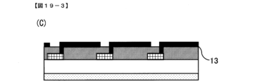
- 1 is a side sectional view showing a manufacturing process of a light emitting device using an LED according to the present invention.
- the light emitting device of the present invention is a light emitting device that includes at least a glass substrate provided with a resin coating film (S) containing at least a siloxane resin, and a light emitter portion.
- the light emitter part is disposed on at least one surface of the glass substrate or the resin coating film (S) so that at least a portion thereof is in contact with the surface.
- the impact resistance of the light emitting device can be increased, the bending resistance can be increased, and the flexibility can be improved. Furthermore, when manufacturing a display, it is possible to prevent the glass from breaking when handling the glass substrate.
- the light emitting body portion is arranged in such a manner that the surface of the glass substrate provided with the resin coating film (S) and the light emitting body portion are in contact with each other without any other member intervening between the surface of the glass substrate and the light emitting body portion. It is more preferable.
- Arranging the light emitting body part in such a manner that the surface and the light emitting body part are in contact with each other without any other member intervening between the surface and the light emitting body part is hereinafter referred to as "forming the light body part directly”. There is.
- the light emitting device 1 using the organic EL of the present invention includes a glass substrate 11 having a resin coating film (S) 23 containing at least a siloxane resin;
- the structure includes an organic EL light emitter section 20 composed of one electrode 13 , a second electrode 18 , an organic EL light emitter 16 , and a pixel dividing layer 19 .
- the impact resistance of the light emitting device 1 using organic EL can be increased, and the bending resistance can be increased, and flexibility can be improved. Furthermore, when manufacturing a display, it is possible to prevent the glass from breaking when handling the glass substrate.
- a resin coating film (S) when forming a resin coating film (S), a flattening layer, a pixel dividing layer, an insulating film, etc. on the glass substrate 11, a polyimide resin or a siloxane resin is contained before being coated on the glass substrate 11.
- the mixture is a resin composition, and when the resin composition is applied to form a film, the film in which the solvent remains in the film of the resin composition is a coated film, and the film that has been dried and just before heat curing is a dried film.
- a film obtained by exposing a dried film to actinic rays such as ultraviolet rays, visible light, electron beams, or X-rays is an exposed film, and a prebaked film is a prebaked film, a dry film, an exposed film, or a prebaked film.
- a film cured by heating is called a resin coated film, resin film or cured film.
- the plate-shaped body has a form in which the glass substrate 11 has a constant thickness and one side of the plane is longer than the thickness.
- the organic EL light emitter portion 20 be provided on the surface 21 of the glass substrate 11 opposite to the surface 22 on which the resin coating film (S) 23 is disposed.
- the bending resistance of the light emitting device 1 using organic EL can be strengthened, so in the case of a top emission type that emits light from the light emitter part 20 in the direction opposite to the glass substrate 11 side, the emission surface that emits light The sides can be folded inward, making the device smaller and more compact.
- the organic EL light emitter part 20 when the organic EL light emitter part 20 is arranged on the surface 21 of the glass substrate 11, the organic EL light emitter part 20 is arranged in such a manner that at least a part of the organic EL light emitter part 20 is in contact with the surface 21 of the glass substrate 11. It is preferable. Further, the organic EL light emitter part is arranged in such a manner that the organic EL light emitter part 20 is in contact with the surface 21 of the glass substrate 11 without any other member interposed between the surface 21 of the glass substrate 11 and the organic EL light emitter part 20. It is more preferable to arrange 20. Thereby, the impact resistance and bending resistance of the light emitting device can be further improved.
- a light emitting device 1 using organic EL according to the present invention will be described in detail.
- a resin coating film (S) 23 is disposed on the surface 22 of the glass substrate 11.
- An organic EL light emitter part 20 is arranged on the surface 21 of the glass substrate 11 opposite to the surface 22 on which the resin coating film (S) 23 is arranged.
- a drive element 28 such as a thin film transistor (hereinafter referred to as TFT) that controls the light emission of the organic EL light emitter 16 may be provided.
- metal wiring may be provided. If necessary, by providing the planarization layer 12, it is possible to cover the metal wiring and the entire surface of the drive element 28, and cover, protect, and planarize the unevenness after the drive element 28 and the like are formed.
- the first electrode 13 is arranged in a certain wiring pattern shape. This first electrode 13 maintains electrical connection with the driving element 28 through a contact hole formed in a part of the planarization layer 12. This arranged first electrode 13 corresponds to the anode of the organic EL light emitter 16.
- a pixel dividing layer 19 is arranged on the surface of the planarization layer 12 on the opposite side to the glass substrate 11 side in a shape that covers a part of the first electrode 13.
- a layer consisting of hole injection layer 14 / hole transport layer 15 / organic EL light emitter 16 / electron transport layer 17 is formed on the first electrode 13, and a second electrode 18 is further formed on the layer in a certain wiring pattern. Arrange by shape.
- the second electrode 18 corresponds to the cathode of the organic EL light emitter 16. It is preferable that the organic EL light emitter 16 and the driving wiring be connected through a contact hole (not shown) formed in the planarization layer 12.
- a light emitting device 1 using organic EL is constructed.
- FIG. 2-1 shows a side cross-sectional view (A) in which the resin coating film (S) 23 is arranged on one plane of the glass substrate 11 and the organic EL light emitter part 20 is arranged on the other plane of the glass substrate 11. show.
- This is a simplified version of the organic EL light emitter portion 20 of the light emitting device 1 using the top emission type organic EL shown in FIG.
- FIG. 2-2 shows a side cross-sectional view (B) of the folded state with the organic EL light emitter part 20, which is the emission surface side from which the emitted light 24 is emitted, facing inside.
- the structure in which the organic EL light emitter part 20 is arranged on the inside and the resin coating film (S) 23 is arranged on the outside of the glass substrate 11 is a structure that can strengthen the bending resistance. Therefore, in a medium for displaying an image, the top emission surface side with the organic EL light emitter portion 20 serving as a display screen can be folded inward.
- the resin coating film (S) 23 and the organic EL light emitter part 20 are laminated in this order on the surface 21 of the glass substrate 11 is preferable.
- the emission surface side that emits light can be folded inward, making it possible to make the device smaller and more compact. Further, by using a glass substrate with excellent transparency and a resin coating film (S) 23 containing a siloxane resin, it is possible to improve the light extraction performance from the light emitting device 1 using organic EL.
- the organic EL light emitter part 20 when the organic EL light emitter part 20 is disposed on the surface of the resin coating film (S) 23, the organic EL light emitter part 20 is arranged in such a manner that at least a part of the organic EL light emitter part 20 is in contact with the surface of the resin coat film (S) 23.
- an EL light emitter portion 20 is provided.
- the organic EL light emitter part 20 is placed on the surface of the resin coated film (S) 23 without any other member interposed between the surface of the resin coated film (S) 23 and the organic EL light emitter part 20. It is more preferable to arrange the organic EL light emitter parts 20 in such a manner that they are in contact with each other. Thereby, the impact resistance and bending resistance of the light emitting device can be further improved.
- FIG. 3 showing a light emitting device 1 using a bottom emission type organic EL
- the electrode configuration is reversed from that of the top emission type shown in FIG. 1, and a resin coating film ( S) 23 is arranged, and the organic EL light emitter part 20 is arranged thereon.
- the structure of the organic EL light emitting body portion 20 has been described above with reference to FIG. 1, so a description thereof will be omitted here.
- a light emitting device using a bottom emission type organic EL that emits light 24 from the organic EL light emitter 16 in the direction toward the glass substrate 11 by using a transparent electrode as the first electrode 13 and a reflective electrode as the second electrode 18. 1 is configured.
- FIG. 4-1 shows a side cross-sectional view (A) in which the resin coating film (S) 23 and the organic EL light emitter part 20 are arranged on one surface of the glass substrate 11.
- FIG. 4-2 shows a side sectional view (B) of a state in which the glass substrate 11, which is the emission surface side from which the emitted light 24 is emitted, is folded inward.
- the structure in which the glass substrate 11 is placed inside and the resin coating film (S) 23 is placed outside of the glass substrate 11 has strong bending resistance. Therefore, the bottom emission surface side with the glass substrate 11 side serving as a display screen can be folded inward.
- resin coating films (S) 23 are disposed on both surfaces of the glass substrate 11, and an organic EL light emitter portion 20 is further disposed on the surface of either resin coating film (S) 23. Laminated structures are preferred.
- FIG. 5 shows a configuration in which a resin coating film (S) 23 is provided not only on one surface 21 of the glass substrate 11 but also on the opposite surface 22.
- the organic EL light emitter part 20 when the organic EL light emitter part 20 is disposed on the surface of the resin coating film (S) 23, the organic EL light emitter part 20 is arranged in such a manner that at least a part of the organic EL light emitter part 20 is in contact with the surface of the resin coat film (S) 23.
- an EL light emitter portion 20 is provided.
- the organic EL light emitter part 20 is placed on the surface of the resin coated film (S) 23 without any other member interposed between the surface of the resin coated film (S) 23 and the organic EL light emitter part 20. It is more preferable to arrange the organic EL light emitter parts 20 in such a manner that they are in contact with each other. Thereby, the impact resistance and bending resistance of the light emitting device can be further improved.
- the flexibility of the film can be increased, and cracks are less likely to occur at wire bends, etc., making it possible to use organic EL. Therefore, it is possible to reduce the defective rate of light emission of the light emitting device 1.
- the content of polyimide resin (B) is preferably 50% by weight or more.
- the content of the polyimide resin (B) is preferably 95% by weight or less, more preferably 75% by weight or less.
- the total solid content refers to all components of the composition contained in each layer.
- the pixel dividing layer 19 can be applied by a wet coating method such as a spin coating method, a slit coating method, a dip coating method, a spray coating method, or a printing method, which can uniformly form a thin film on a large substrate.
- the thickness of the pixel dividing layer 19 is preferably at least ten times the thickness of the first electrode 13.
- it since it also supports the structure covering the second electrode in the subsequent process and affects the strength of the light emitting device, it is also effective to design it in an appropriate step-like manner.
- the flexibility of the film can be increased, and cracks may occur at the bent portions of the wiring. is less likely to occur, and the rate of defective light emission of the light emitting device 1 using organic EL can be lowered.
- the planarization layer 12 can be applied by a wet coating method such as a spin coating method, a slit coating method, a dip coating method, a spray coating method, or a printing method, which can uniformly form a thin film on a large substrate.
- a wet coating method such as a spin coating method, a slit coating method, a dip coating method, a spray coating method, or a printing method, which can uniformly form a thin film on a large substrate.
- the range of the light emitting pixel formed by the organic EL light emitter part 20 is the range where the first electrode 13 and the second electrode 18, which are arranged opposite to each other, intersect and overlap.
- the planar shape of the light emitting pixel may be, for example, rectangular or circular, and can be easily changed depending on the shape of the pixel dividing layer.
- organic EL light emitters 16 having emission peak wavelengths in red, green, and blue regions are arranged, or white organic EL light emitters 16 are fabricated over the entire surface and used in combination with a separate color filter. is called a color display.
- the peak wavelength of the light to be displayed is in the range of 560 to 700 nm, in the green region 300 to 560 nm, and in the blue region 420 to 500 nm.
- a passive matrix type in which electrodes are divided into columns and rows and only the pixels sandwiched between the electrodes emit light
- a passive matrix type in which several TFTs are used for each pixel. It is broadly classified into an active matrix type, which is provided in an active matrix type for switching, but is not particularly limited to the active matrix type.
- the first electrode 13 or the second electrode 18 in this embodiment is preferably a light-transmissive or light-reflective electrode selected from a top emission or bottom emission mode.
- the first electrode 13 in this embodiment is preferably a light-reflective conductive film in the case of a top-emission type, and a light-transmissive conductive film in the case of a bottom-emission type.
- the second electrode 18 in this embodiment is preferably a light-reflective conductive film in the case of a bottom-emission type, and a light-transmissive conductive film in the case of a top-emission type.
- the resistance of the electrode is not limited as long as sufficient current can be supplied for light emission of the light emitting element, but from the viewpoint of power consumption of the organic EL light emitter 16, a low resistance is preferable.
- ITO with a resistance of 300 ⁇ / ⁇ or less can function as an element electrode, but since it is also possible to supply a substrate with a resistance of about 10 ⁇ / ⁇ , it is particularly preferable to use a low-resistance product.
- the thickness of the electrode can be arbitrarily selected according to characteristics such as transmittance and resistance value, but it can usually be used within a range of 100 to 300 nm.
- conductive metal oxides such as transparent tin oxide, indium oxide, and indium tin oxide (ITO), metals such as gold, silver, and chromium, inorganic conductive substances such as copper iodide and copper sulfide, polythiophene, and polypyrrole.
- Conductive polymers such as and polyaniline can be used, but are not particularly limited.
- the first electrode 13 and the second electrode 18 are required to have contrasting characteristics.
- the second electrode 18 is required to function as a cathode that can efficiently inject electrons, metal materials are often used in consideration of the stability of the electrode. Note that it is also possible to use the first electrode 13 as a cathode and the second electrode 18 as an anode.
- Al, Mg, Ag, and the like are known as materials for use as the cathode, and are formed by a vacuum film-forming method similarly to the organic EL light emitter 16, but are not particularly limited.
- the organic EL light emitter part 20 in this embodiment has the form of hole injection layer 14/hole transport layer 15/organic EL light emitter 16/electron transport layer 17 from the glass substrate 11 side.
- hole injection layer 14/hole transport layer 15/organic EL light emitter 16/electron transport layer 17 from the glass substrate 11 side.
- it is not limited to this. It may be either a hole transport layer/emissive layer/electron transport layer or a emissive layer/electron transport layer.
- Each layer can be formed by a known method. For example, it can be formed by a mask vapor deposition method or an inkjet method.
- the thickness of each layer is generally selected from 1 to 200 nm in consideration of the resistance value of each layer material and the effect on the extraction efficiency of EL light emission.
- the organic EL light emitter 16 the injected electrons and holes recombine to emit light.
- the organic EL light emitter may have a single layer or multiple layers, and may be composed of a mixture of a host material and a dopant material, or may be composed of a host material alone. That is, the organic EL light emitter 16 may be made of a single material and emit light, only the host material or the dopant material may emit light, or both the host material and the dopant material may emit light. From the viewpoint of efficiently utilizing electrical energy and obtaining light with high color purity, the organic EL light emitter 16 is preferably made of a mixture of a host material and a dopant material.
- the host material and the dopant material may each contain two or more kinds of materials.
- the hole transport layer 15 is formed by laminating or mixing one or more hole transport materials, or by using a mixture of a hole transport material and a polymer binder. Alternatively, the hole transport layer may be formed by adding an inorganic salt such as iron(III) chloride to the hole transport material.
- the hole transporting material is not particularly limited as long as it is a compound that can form a thin film necessary for manufacturing a light emitting element, can inject holes from the first electrode, and can further transport holes.
- the resin coating film (S) 23 in the present invention is a cured film of a resin composition containing a siloxane resin.
- the resin coating film (S) 23 in the present invention is a "cured film” because the siloxane resin in the resin composition undergoes a condensation reaction (thermal crosslinking) of silanol groups or a radical addition reaction (photo-optical) of radically polymerizable groups. (crosslinking).
- thermal crosslinking thermal crosslinking of silanol groups
- photo-optical radical addition reaction
- crosslinking By conducting IR analysis of the cured film, it is possible to determine whether or not it is crosslinked based on the presence or absence of peaks of silanol groups or double bonds.
- the resin coating film (S) 23 is such that when an impact is applied to the glass substrate 11, the glass substrate 11 may be damaged starting from micro cracks existing on the glass surface, or the resin coating film (S) 23 may cause the glass substrate 11 to S)
- it is a reinforced film that prevents the glass substrate 11 from breaking starting from micro-cracks at the bent portion when it is bent with 23 on the outside, and improves the impact resistance and bending resistance of the glass substrate 11. .
- the light emitting device 41 using the LED 42 of the present invention includes a glass substrate 45 coated with a resin coating film (S) 47 containing at least siloxane resin, and at least wiring 44. , a resin film (A) 43 that is in contact with at least a portion of the wiring 44 and an LED light emitter portion 48 that is composed of the LED 42.
- S resin coating film
- A resin film
- the impact resistance of the light emitting device 41 using the LED 42 can be increased, the bending resistance can be increased, and the flexibility can be improved. Furthermore, when manufacturing a display, it is possible to prevent the glass from breaking when handling the glass substrate.
- the resin coating film (S) 47 and the LED light emitter portion 48 are laminated in this order on either surface 49 of the glass substrate 45.
- the LED light emitter part 48 when disposing the LED light emitter part 48 on the surface of the resin coating film (S) 47, the LED light emitter part 48 is placed in such a manner that at least a part of the LED light emitter part 48 is in contact with the surface of the resin coating film (S) 47. Preferably, a portion 48 is provided. Furthermore, the LED light emitter part 48 is in contact with the surface of the resin coat film (S) 47 without any other member interposed between the surface of the resin coat film (S) 47 and the LED light emitter part 48. It is more preferable to arrange the LED light emitter portion 48 in the following manner. Thereby, the impact resistance and bending resistance of the light emitting device can be further improved.
- FIG. 6 illustrates a bottom emission type in which light is emitted from the glass substrate 45 side (lower side in FIG. 6), in which a resin coating film (S) 47 is disposed on the surface 49 of the glass substrate 45, and an LED light emitter portion is placed on top of the resin coating film (S) 47. 48.
- the configuration of the LED light emitter portion 48 is such that a plurality of LEDs 42 each having an electrode 46 are arranged on a resin coating film (S) 47, and a resin film (A) 43 is arranged on the LEDs 42.
- the LED 42 has a polygonal solid shape, such as a tetrahedron, a rectangular parallelepiped, a hexahedron such as a cube, and the like. Further, their surfaces may have irregularities.
- Two different surfaces refer to, in a polygonal three-dimensional LED 42 having two or more surfaces, when one of the surfaces having the electrode 46a is used as a reference surface, the other electrode 46b is placed on a surface different from the reference surface. Indicates that it has. Note that in the present invention, the electrodes 46a and 46b are used to clearly indicate the parts, and the electrodes 46 are still the same. Moreover, the electrode 46 provided in the LED 42 refers to a connection portion for transmitting a signal from the wiring to the LED for controlling the light emission of the LED 42.
- the polygonal three-dimensional LED 42 has one electrode 46a on the surface facing the resin coating film (S) 47 and the other electrode 46b on the opposite surface.
- One electrode 46a is connected to a wiring 44c arranged on the surface on the resin coating film (S) 47 side, and the other electrode 46b is connected to a wiring 44d extending in the resin film (A) 43.
- the wiring 44 is in contact with the resin film (A) 43, and the wiring 44c, the wiring 44d, and the wiring 44e to be described later are for clearly indicating the parts, and are not the wiring 44. There isn't.
- FIGS. 7 to 9 only the arrangement of the electrode 46 by the LED 42, the electrode 46, the wiring 44, and the resin film (A) 43 is shown in FIGS. 7 to 9.
- the following is an example of a mode that expresses the following.
- FIG. 7 illustrates a structure in which the electrodes 46 are arranged laterally on opposing surfaces with the LED 42 in between
- FIG. 8 illustrates a structure in which the electrodes 46 are provided on adjacent surfaces of the LED 42.
- FIG. 9 illustrates a structure in which electrodes 46 are arranged on each discontinuous surface of an LED 42 having discontinuous surfaces.
- a discontinuous surface is not a continuous surface, but a surface with steps, etc.
- the LED 42 has a configuration in which the electrodes 46 are provided on two different surfaces, but the LED 42 has a configuration in which a pair of electrodes 46 are provided on one of the surfaces. It is also preferable to
- FIG. 10 shows a light emitting device 41 using an LED 42 provided with a pair of electrodes 46 on either side.
- the light emitting device 41 has a resin coating film (S) 47 arranged on a glass substrate 45, a plurality of LEDs 42 arranged thereon, and a resin film (A) 43 arranged on the LEDs 42.
- the LED 42 includes a pair of electrodes 46 on a surface opposite to the surface in contact with the resin coating film (S) 47, and each electrode 46 is connected to a wiring 44 extending in the resin film (A) 43. If the wiring 44 extending in the resin film (A) 43 is covered with the resin film 43 (A), the resin film 43 (A) also functions as an insulating film, so that it maintains electrical insulation. It is configured to do this. Thereby, the light extraction efficiency of the emitted light 50 from the LED 42 can be increased, and the adhesiveness between the resin coating film (S) 47 and the LED 42 can be improved.
- a plurality of resin films (A) 43 are further laminated on the resin film (A) 43 disposed so as to be in contact with at least a portion of the LED 42, for a total of three layers.
- the resin film (A) 43 may have a single layer or multiple layers. Note that if the wiring 44 extending in the resin film (A) 43 is covered with the resin film (A) 43, the resin film (A) 43 also functions as an insulating film, so that it has electrical insulation properties. It is configured to hold.
- the wiring 44 having a structure that maintains electrical insulation means that a portion of the wiring 44 that requires electrical insulation is covered with the resin film (A) 43.
- a light emitting device 41 using a bottom emission type LED that emits light 50 from the LED 42 in the direction toward the glass substrate 45 is configured.
- the light emitting diode light emitter portion 48 is provided on the surface 49 of the glass substrate 45 on the opposite side to the surface 51 on which the resin coating film (S) 47 is disposed.
- the LED light emitter part 48 is arranged on the surface 49 of the glass substrate 45, it is preferable that the LED light emitter part 48 is arranged in such a manner that at least a part of the LED light emitter part 48 is in contact with the surface 49 of the glass substrate 45. . Further, the LED light emitting body portion 48 is arranged in such a manner that the LED light emitting body portion 48 is in contact with the surface 49 of the glass substrate 45 without any other member interposed between the surface 49 of the glass substrate 45 and the LED light emitting body portion 48. It is more preferable to do so. Thereby, the impact resistance and bending resistance of the light emitting device can be further improved.
- FIG. 11 illustrates a top emission type, in which an LED light emitter part 48 is arranged on a surface 49 of a glass substrate 45, and a surface 51 of the glass substrate 45 opposite to the front surface 49 on which the LED light emitter part 48 is arranged, This is a configuration in which a resin coating film (S) 47 is arranged.
- the configuration of the LED light emitting body part 48 is such that the LED 42 having electrodes 46a and 46b is placed on the glass substrate 45, and the resin film (A) 43 is placed on the glass substrate 45 and the LED 42. Further, wirings 44c and 44d are connected to the electrodes 46a and 46b, respectively, and a signal for controlling the light emission of the LED 42 is transmitted to the LED through the wiring 44. Similar to FIG. 6, drive elements and the like are omitted.
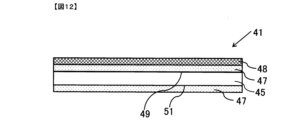
- the light emitting device 41 further includes the resin coating film (S) 47 on the surface 51 of the glass substrate 45 opposite to the surface 49 on which the resin coating film (S) 47 is disposed. It is preferable to do so.
- resin coating films (S) 47 are arranged on both surfaces of the glass substrate 45, and a light emitting diode light emitter portion 48 is further disposed on the surface of either resin coating film (S) 47. It is preferable to have a laminated structure.
- the LED light emitter part 48 when disposing the LED light emitter part 48 on the surface of the resin coating film (S) 47, the LED light emitter part 48 is placed in such a manner that at least a part of the LED light emitter part 48 is in contact with the surface of the resin coating film (S) 47. Preferably, a portion 48 is provided. Furthermore, the LED light emitter part 48 is in contact with the surface of the resin coat film (S) 47 without any other member interposed between the surface of the resin coat film (S) 47 and the LED light emitter part 48. It is more preferable to arrange the LED light emitter portion 48 in the following manner. Thereby, the impact resistance and bending resistance of the light emitting device can be further improved.
- FIG. 12 shows a configuration in which a resin coating film (S) 47 is provided not only on one surface 49 of the glass substrate 45 but also on the opposite surface 51.
- S resin coating film
- the materials for the wirings 44, 44c, 44d and the electrodes 46, 46a, 46b are not particularly limited, and include metals, conductive films, etc., and known materials may also be used. Metals are preferable from the viewpoint of electron mobility, and examples thereof include gold, silver, copper, aluminum, nickel, titanium, molybdenum, and alloys containing these. These metals can be produced by, for example, wet plating such as electroless plating and electrolytic plating, CVD chemical vapor deposition (CVD) such as thermal CVD, plasma CVD, and laser CVD, dry plating methods such as vacuum evaporation, sputtering, and ion plating. It can be formed by etching after bonding the metal foil to the substrate.
- CVD chemical vapor deposition such as thermal CVD, plasma CVD, and laser CVD
- dry plating methods such as vacuum evaporation, sputtering, and ion plating. It can be formed by etching after bonding the metal foil to the substrate.
- the conductive film is preferable from the viewpoint of transparency, and is made of, for example, a compound containing as a main component an oxide of at least one element selected from indium, gallium, zinc, tin, titanium, niobium, etc., an organic substance, and conductive particles.
- a compound containing as a main component an oxide of at least one element selected from indium, gallium, zinc, tin, titanium, niobium, etc. examples include photosensitive conductive paste, but other known materials may also be used.
- Examples of compounds containing as a main component an oxide of at least one element selected from indium, gallium, zinc, tin, titanium, niobium, etc. include indium tin zinc oxide (ITZO), indium gallium zinc oxide, etc.
- IGZO InGaZnO
- zinc oxide ZnO
- indium zinc oxide IZO
- indium gallium oxide IGO
- indium tin oxide ITO
- indium oxide InO
- These conductive films can be formed by wet plating such as electroless plating or electrolytic plating, CVD chemical vapor deposition (CVD) such as thermal CVD, plasma CVD, or laser CVD, or dry plating such as vacuum evaporation, sputtering, or ion plating. It can be formed by, for example, a method in which a metal foil is bonded to a substrate and then etched.
- CVD chemical vapor deposition such as thermal CVD, plasma CVD, or laser CVD
- dry plating such as vacuum evaporation, sputtering, or ion plating. It can be formed by, for example, a method in which a metal foil is bonded to a substrate and then etched.
- the content of the conductive particles is preferably 60% by mass or more and 90% by mass or less.
- the conductive layer contains an organic substance, disconnection can be suppressed on curved surfaces and bent portions, and conductivity can be improved.
- the content of the conductive particles is less than 60% by mass, the probability of contact between the conductive particles becomes low, and the conductivity decreases. Further, the conductive particles tend to separate from each other at the bent portion of the wiring.
- the content of conductive particles is preferably 70% by mass or more.
- the content of the conductive particles exceeds 90% by mass, it becomes difficult to form a wiring pattern, and disconnections are likely to occur at bent portions.
- the content of conductive particles is preferably 80% by mass or less.
- organic substances include epoxy resins, phenoxy resins, acrylic copolymers, and epoxy carboxylate compounds. Two or more types of these may be contained. It may also contain an organic substance having a urethane bond. By containing an organic substance having a urethane bond, the flexibility of the wiring can be improved.
- the organic substance preferably exhibits photosensitivity, and a fine wiring pattern can be easily formed by photolithography.
- Photosensitivity is developed by, for example, containing a photopolymerization initiator and a component having an unsaturated double bond.
- the conductive particles in the present invention refer to particles made of a substance having an electrical resistivity of 10 ⁇ 5 ⁇ m or less.
- the material constituting the conductive particles include silver, gold, copper, platinum, lead, tin, nickel, aluminum, tungsten, molybdenum, chromium, titanium, indium, alloys of these metals, and carbon particles.
- the average particle diameter of the conductive particles is preferably 0.005 ⁇ m or more and 2 ⁇ m or less.
- the average particle diameter here refers to the average particle diameter of large-diameter particles when two or more types of conductive particles are contained.
- the average particle diameter of the conductive particles is more preferably 0.01 ⁇ m or more.
- the average particle diameter of the conductive particles is 2 ⁇ m or less, it becomes easier to form a desired wiring pattern.
- the average particle diameter of the conductive particles is more preferably 1.5 ⁇ m or less.
- the thickness of the conductive film is preferably 2 ⁇ m or more and 10 ⁇ m or less. When the thickness of the conductive film is 2 ⁇ m or more, disconnection at the bent portion can be further suppressed and the conductivity can be further improved.
- the thickness of the conductive film is more preferably 4 ⁇ m or more. On the other hand, when the thickness of the conductive film is 10 ⁇ m or less, a wiring pattern can be more easily formed in the manufacturing process.
- the thickness of the conductive film is more preferably 8 ⁇ m or less.
- FIG. 13 shows an embodiment in which the light emitting device 41 shown in FIG. 6 is further provided with an LED driving board 52 and a driving element 53 having a driver IC added thereto.
- the LED driving board 52 provided at a position facing the glass substrate 45 and the driving element 53 added thereto are electrically connected through wirings 44c and 44e, so that the light emission of the LEDs 42 can be controlled.
- the drive element 53 is electrically connected to the wiring 44c via a bump 55, for example.
- a barrier metal 54 may be provided to prevent diffusion of metal such as the wiring 44.
- the driving element 53 may be arranged in the resin film (A) 43 on the glass substrate 45 near the LED 42, or the driving element 53 may be arranged above the LED 42 using a resin film (A) 43.
- a configuration in which it is arranged in the membrane (A) 43 is also preferable.
- the wiring 44e extends on the side surface of the LED driving board 52.
- a plurality of LEDs can be individually switched and driven, and the height of the light emitting device itself is reduced and high-speed response is improved.
- the light emitting device can be made smaller and have a narrower frame.
- the LED drive board 52 is not particularly limited, and any known one can be used. Examples include glass substrates, sapphire substrates, printed wiring boards, TFT array substrates, and ceramics. When using a printed wiring board, it is possible to connect to the driving element 53, the bumps 55, the wiring 44, etc. without forming the wiring 44e.
- a thin film transistor (hereinafter sometimes referred to as TFT) 56 and a TFT insulating film 57 are added in the resin film (A) 43.
- the arrangement is shown in FIG. 14. It can be formed on the resin coating film (S) 47 by a chemical vapor deposition technique or a sputtering technique.
- One of the LED display methods it is clear, has a high response speed, and can achieve good contrast.
- the driving methods for the light emitting device 41 using LEDs include a passive matrix type in which electrodes are divided into columns and rows and only the pixels sandwiched between the electrodes emit light, and a switching method in which several TFTs are provided in each pixel. Although it is broadly classified into active matrix type, it is not particularly limited.
- the entire thickness of the resin film (A) 43 is 5 ⁇ m or more and 100 ⁇ m or less.
- the light emitted from the LED 42 in all directions can be suppressed from being absorbed in the resin film (A) 43, the light extraction efficiency can be increased, and the brightness can be improved. Furthermore, it is possible to reduce the height of the light-emitting device itself using LEDs, to suppress wiring defects such as short circuits by shortening the wiring distance, to suppress reduction in loss, and to improve high-speed response.
- the total thickness of the resin film (A) 43 refers to the thickness of the entire layer of continuous resin films (A) in which at least a portion of one resin film (A) is in contact with another resin film (A).
- the overall thickness is preferably 5 ⁇ m or more and 100 ⁇ m or less, more preferably 8 ⁇ m or more and 60 ⁇ m or less.
- the number of layers of the resin film (A) 43 is 2 or more and 10 or less.
- the resin film (A) 43 preferably has one or more layers, and furthermore, by having two or more layers, the number of wirings that can be connected to the LEDs can be increased.
- the number of layers is preferably 10 or less, from the viewpoint of suppressing wiring defects such as short circuits due to reduction in package height and short wiring distance, reducing loss, and improving high-speed response.
- the surface of the LED 42 other than the light extraction surface is covered with the resin film (A) 43 in a manner in contact with the LED 42, but the LED 42 is not necessarily covered with the resin film (A) 43. It is not necessary to cover the LED 42 with the resin film (A) 43 in a manner in which it is in contact with the resin film (A) 43, and as shown in FIG.
- the length of one side of the LED 42 is 5 ⁇ m or more and 700 ⁇ m or less, and more preferably the length of one side is 5 ⁇ m or more and 100 ⁇ m or less.
- An LED is composed of a PN junction in which a P-type semiconductor and an N-type semiconductor are joined, and when a forward voltage is applied to the LED, electrons and holes move within the chip, causing current to flow. At this time, an energy difference is created by the combination of electrons and holes, and the surplus energy is converted into light energy, which emits light.
- the wavelength of light emitted from an LED varies depending on the compound that constitutes the semiconductor, such as GaN, GaAs, InGaAlP, and GaP, and this difference in wavelength determines the color of the emitted light.
- white is generally displayed by mixing two or more different colors of light, but in the case of LEDs, color reproducibility is greatly improved by mixing the three primary colors of red, green, and blue. This has been improved, making it possible to display a more natural white color.
- the shape of the LED includes a bullet shape, a chip shape, a polygonal shape, etc., but a chip shape and a polygonal shape are preferable from the viewpoint of miniaturization of the LED. Further, it is preferable that the length of one side of the LED is 5 ⁇ m or more and 700 ⁇ m or less, since this allows a plurality of chips to be arranged, and it is more preferable that the length of one side of the LED is 5 ⁇ m or more and 100 ⁇ m or less.
- the reflective film 59 can be provided at any location on the resin film (A) 43, and can be arranged so as to surround it on all sides with respect to the direction in which the LED 42 is taken out, arranged diagonally with respect to the LED 42, or curved. It is also possible to arrange them side by side.
- the reflective film may be any film that reflects light, such as aluminum, silver, copper, titanium, and alloys containing these, but is not limited to these.
- a partition wall 60 between the plurality of LEDs 42 having a thickness greater than the thickness of the LEDs 42.
- partition walls 60 in a repeating pattern corresponding to the number of pixels of the light emitting device 41, that is, between or around each LED 42. This configuration is preferable because it facilitates bonding with the resin coating film (S) 47 that may include the wiring 44d. Further, by disposing the partition wall 60, it is possible to use it as a mark when transferring the LED later, and it can also be used as a photo spacer, so that the efficiency at the time of LED transfer can be improved, which is preferable.
- FIG. 17 shows a configuration in which the resin film (A) 43 is not disposed so as to be in contact with a part of the periphery of the partition wall, the resin film (A) 43 that covers the LEDs 42 is provided between or around a plurality of LEDs 42. It is also a preferable embodiment to provide a partition wall 60 at.
- the thickness of the partition wall 60 is preferably larger than the thickness of each LED, and specifically, preferably 1 ⁇ m or more and 120 ⁇ m or less.
- the partition wall 60 may be made of a resin film (A), and the resin film (A) may be made of a material such as epoxy resin, (meth)acrylic polymer, polyurethane, polyester, polyolefin, or polysiloxane.
- the resin (M) described below may be used.
- a light shielding portion may be provided on the side surface of the partition wall 60 or on the partition wall itself.
- the light shielding portion is a portion containing, for example, a black pigment.
- the light emitted from the LED toward the partition wall can be reflected to increase the light extraction efficiency, and a reflective film may be provided on the side surface of the partition wall to improve the brightness.
- a light shielding layer between the plurality of LEDs.
- a light shielding layer between a plurality of LEDs, it is possible to suppress light leakage from the LEDs and color mixture between pixels and improve contrast without significantly impairing light extraction efficiency.
- the light-shielding layer may be composed of a resin film (A) containing (E) a coloring material, or may be composed of a known material such as an epoxy resin, (meth)acrylic polymer, polyurethane, polyester, polyolefin, or polysiloxane. It's okay.
- a black pigment may be used, such as black organic pigments such as carbon black, perylene black, and aniline black, graphite, and titanium, copper, iron, manganese, cobalt, chromium, nickel, and zinc.
- metal fine particles such as calcium and silver
- inorganic pigments such as metal oxides, composite oxides, metal sulfides, metal nitrides, and metal oxynitrides.
- it may be made black by combining a red pigment, a blue pigment, and, if necessary, a yellow pigment or other pigments.
- a dye may also be used. Two or more types of colorants may be contained.
- the thickness of the glass substrate 11 and the glass substrate 45 is preferably 0.03 to 0.3 mm.
- the thickness of the glass substrate By setting the thickness of the glass substrate to 0.03 mm or more, the impact resistance of the glass can be ensured, and by setting the thickness to 0.3 mm or less, bending resistance can be ensured. Preferably it is 0.04 to 0.2 mm, more preferably 0.05 to 0.1 mm.
- the type of glass substrate can be used without any particular limitation, but common glasses containing SiO 2 (silicon oxide) as a main component, such as soda lime silicate glass, aluminosilicate glass, borosilicate glass, Non-alkali glass, quartz glass, etc. are used.
- SiO 2 silicon oxide
- the glass substrate 11 and the glass substrate 45 are glass substrates that have been subjected to a reinforcement treatment. Thereby, the bending resistance of the light emitting device can be improved.
- the strengthened glass substrate has a compressive stress layer on the glass surface.
- Methods for forming the compressive stress layer include, for example, a physical strengthening method that utilizes the expansion and contraction of glass by heating and cooling, and a chemical strengthening method that exchanges alkali ions in the glass with other alkali ions with a larger ionic radius.
- a physical strengthening method that utilizes the expansion and contraction of glass by heating and cooling
- a chemical strengthening method that exchanges alkali ions in the glass with other alkali ions with a larger ionic radius.
- chemically strengthened glasses aluminosilicate chemically strengthened glass, soda lime chemically strengthened glass, etc. are more preferable.
- chemically strengthened ultra-thin glass include “Xensation” (registered trademark) series (manufactured by Schott), “Corning” (registered trademark), “Gorilla” (registered trademark) Glass series (manufactured by CORNING), " Examples include the “Dinorex” (registered trademark) series (manufactured by Nippon Electric Glass Co., Ltd.) and the “Dragontrail” (registered trademark) series (manufactured by AGC Corporation).
- the thickness of the resin coating film (S) 23 and the resin coating film (S) 47 is preferably 1 to 10 ⁇ m.
- the thickness of the resin coating film (S) is preferably 1.2 to 7 ⁇ m, more preferably 1.4 to 5 m, even more preferably 1.5 to 2 ⁇ m.
- the resin coating film (S) 23 and the resin coating film (S) 47 contain inorganic particles.
- the hardness of the resin coating film (S) can be improved and the refractive index of the resin coating film (S) can be adjusted appropriately.
- the inorganic particles include silicon compound particles, aluminum compound particles, tin compound particles, titanium compound particles, zirconium compound particles, barium compound particles, etc., and can be appropriately selected depending on the purpose. In order to more easily adjust the refractive index, silica particles, zirconium oxide particles, and titanium oxide particles are preferred.
- the inorganic particles include silica particles.
- the light emitting device can achieve both high levels of bending resistance and transparency.
- the content of silica particles is preferably 10% by weight or more and 40% by weight or less in the total solid of the resin coating film (S).
- the total solid content refers to all components other than the solvent in the resin coating film (S) containing the siloxane resin.
- the content of silica particles By setting the content of silica particles to 10% by weight or more in the total solid content, crosslinking is promoted by the silanol condensation reaction between the siloxane resin and the silica particles, and the degree of crosslinking of the resin coating film (S) in the present invention is increased. , the bending resistance can be further improved. Moreover, the difference in refractive index between the glass substrate and the resin coating film (S) can be reduced, and unevenness caused by variations in the film thickness of the resin coating film (S) can be reduced. By controlling the content of silica particles to 40% by weight or less based on the total solid content, a resin coating film (S) with good bending resistance and adhesion can be obtained.
- the average particle diameter of the silica particles is preferably 1 to 200 nm, more preferably 1 to 70 nm, from the viewpoint of further improving the transparency of the resin coating film (S) in the present invention.
- the average particle diameter of the silica particles can be determined by a dynamic light scattering method. Specifically, a dispersion liquid with a silica particle concentration of 10 to 30% by weight is irradiated with light at a wavelength of 780 nm using a semiconductor laser, the scattered light is measured, and the average value is determined by frequency analysis using the FFT-heterodyne method. Particle size can be determined.
- silica particles examples include the product name "sicastar” (sold by Corefront Co., Ltd.) and “Rheolo Seal” (registered trademark) (manufactured by Tokuyama Co., Ltd.). These may be used after being pulverized or dispersed using a dispersing machine such as a bead mill.
- silica particle dispersions examples include IPA-ST, MIBK-ST, IPA-ST-L, IPA-ST-ZL, PGM-ST, PMA-ST (all manufactured by Nissan Chemical Industries, Ltd.), " “Oscar” (registered trademark) 101, “Oscar” (registered trademark) 105, “Oscar” (registered trademark) 106, “Cataroid” (registered trademark)-S (all manufactured by JGC Catalysts & Chemicals Co., Ltd.), “Quartron” (Registered trademarks) PL-1-IPA, PL-1-TOL, PL-2L-PGME, PL-2L-MEK, PL-2L, GP-2L (all manufactured by Fuso Chemical Industry Co., Ltd.), etc. . Two or more types of these may be contained.
- the absolute value of the difference between the refractive index n1 of the glass substrate 11 and the glass substrate 45 and the refractive index n2 of the resin coating film (S) 23 and the resin coating film (S) 47 is dn Then, it is preferable that dn ⁇ 0.05.
- the difference in refractive index between the glass substrate and the resin coating film (S) By reducing the difference in refractive index between the glass substrate and the resin coating film (S), it is possible to achieve high transmittance and suppress interference unevenness.
- dn exceeds 0.05, interference unevenness tends to occur easily.
- the difference in refractive index between the glass substrate (1.48 to 1.52) and the resin coating (S) By reducing the difference in refractive index between the glass substrate (1.48 to 1.52) and the resin coating (S), loss of transmitted light at the interface between the glass substrate and the resin coating (S) can be reduced.
- unevenness caused by the thickness of the resin coating film (S) can be made less visible, thereby further improving the appearance.
- the refractive index in the present invention can be measured by a prism coupler method.
- the refractive index n1 of the glass substrate varies depending on the type of glass used, but is generally 1.40 or more and 1.60 or less.
- the refractive index n2 of the resin coating film (S) can be easily adjusted by appropriately adjusting the refractive index of the resin component contained therein, as well as by adding inorganic particles having different refractive indexes as described above. Can be done.
- the resin coating film (S) 23 and the resin coating film (S) 47 coated on the glass substrate 11 and the glass substrate 45 are located on the outside, and the glass substrate 11 and the glass substrate 45 are located on the inside. It is preferable to have a bendable portion.
- a light emitting device 1 using organic EL will be explained as an example.
- the resin coating film (S) 23 By disposing the resin coating film (S) 23 on the glass substrate 11, the bending resistance can be improved, and as shown in FIG. 2-2 (B) or FIG. It can be folded with the light emitting surface side from the EL light emitter section 20 facing inside.
- a foldable structure can be realized, and the device itself can be made more compact.
- the side view (B) of FIG. 2-2 shows a state in which the organic EL light emitter part 20, which is the light emitting surface side, is folded inward, and the bent angle 32 is 180 degrees.
- a solid line 30 indicates the plane position of the organic EL light emitter part 20 before folding
- a dashed line 31 indicates the plane position of the organic EL light emitter part 20 after partially folding. shows.
- the transition of the angle from the solid line 30 to the dashed-dotted line 31 after folding is defined as the bent angle 32.
- FIG. 18-1(A) shows a side cross section of the light emitting device 1 before being bent, in which the resin coating film (S) 23 and the organic EL light emitter part 20 are arranged in this order on one surface 21 of the glass substrate 11.
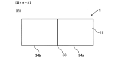
- 18-2(B) is a plan view of the light-emitting device 1
- FIG. 13-3(C) is a perspective view showing the light-emitting device 1 in a bent state
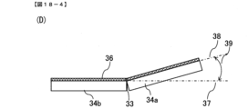
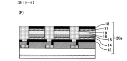
- FIG. 18-4(D) to FIG. 18-6(F) shows a side sectional view showing the bent state.
- FIG. 18-1(A) shows an organic EL light emitter part of a light-emitting device 1 using an organic EL that emits light 10 from the glass substrate 11 side (from above in FIG. 18-1(A)) shown in FIG. This is a simplified version of 20.
- a rectangular light emitting device 1 is illustrated as shown in FIG. A configuration in which the glass substrates 11 are bent to face each other from the left and right directions is illustrated. Further, depending on the specifications of the light emitting device 1, it is also preferable that the bent portion 33 is provided at the center of the short side, and the glass substrate 11 is bent so as to face each other from the top and bottom directions in the figure.
- FIG. 18-2(B) to FIG. 18-6(F) show one light-emitting device member 34a and the other light-emitting device member 34b of the light-emitting device 1 divided by the bent portion 33, and FIG. As shown in C), bend in the direction of arrow 35.
- the glass substrate 11, the resin coating film (S) 23 disposed on one surface 21 of the glass substrate 11, and the organic EL light emitter portion 20 The member including the above is referred to as the glass resin film portion 36 and is simply described.
- the light emitting device members 34a and 34b are examples of portable display devices in which a drive circuit for driving light emission of an organic EL light emitter, circuit members for signal processing, wireless transmission and reception, and the like are built-in.
- a glass resin film portion 36 is arranged on one surface of the light emitting device members 34a and 34b so that the organic EL light emitter portion 20 is located on the light emitting device member 34 side, and is bent in a direction such that the glass substrate 11 side is located on the inside. .
- the light emitting device member 34a and the light emitting device member 34b which are divided by the bending part 33, are connected by a known hinge structure, but the glass resin film part 36 is not divided by the bending part 33, It can be bent while maintaining the appearance of one continuous, integrated member.
- FIG. 18-4(D) shows a state in which the light emitting device member 34a is moved and bent using the bending portion 33 relative to the light emitting device member 34b as a fulcrum (upward in the drawing).
- the planar direction of the glass resin film portion 36 of the light emitting device member 34b is defined as a reference plane 37, and the light emitting device member 34a is bent so that an acute angle difference 39 from the reference plane 38 of the light emitting device member 34a is 5°. .
- FIG. 18(E) shows a state in which the light emitting device member 34a is further moved and bent using the bending portion 33 as a fulcrum.
- the light emitting device member 34a is bent so that an acute angle difference 39 between the reference surface 38 of the light emitting device member 34a and the reference surface 37 of the glass resin film portion 36 of the light emitting device member 34b becomes a right angle of 90°.
- FIG. 18-6(F) shows a state in which the light-emitting device member 34a is further moved and bent by 180° from the original position in FIG. 18-1(A) using the bent portion 33 as a fulcrum.
- the glass substrate 11 of the light emitting device member 34a and the glass substrate 11 of the light emitting device member 34b are bent to a position where they face each other in parallel.
- the glass resin film portion 36 according to the present invention can be bent using the bent portion 33 as a fulcrum to a position where the glass substrate 11 of the light emitting device member 34a and the glass substrate 11 of the light emitting device member 34b face each other in parallel. It is something to do.
- FIG. 18-7(G) shows an enlarged side cross-sectional view of the bent state of the glass resin film portion 36 surrounded by the dashed line 40 in FIG. 18-6(F).
- the glass substrate 11, the resin coating film (S) 23 disposed on one surface 21 of the glass substrate 11, and the organic EL light emitter portion 20 reach a position where the glass substrate 11 faces in parallel with the bent portion 33 as a fulcrum. It is in a bent state.
- the configuration is illustrated in which the glass substrate 11 does not come into contact with each other due to the shape of the touch sensor panel and the housing of the light emitting device (not shown).
- the bending portion 33 shown by the solid line is intended to indicate the point where the bending radius is the minimum, and does not indicate that wrinkles or bent creases remain here.
- the light emitting device member 34a and the light emitting device member 34b can be bent to a position where the glass substrate 11 faces each other in parallel, so that the emitted light 24 is emitted when the light emitting device using organic EL is used as a display device. It is possible to realize a foldable structure in which the display side is hidden inside, and the device itself can be made compact and portable.
- the resin coating film (S) 23 and the resin coating film (S) 47 in the present invention are films obtained by curing a resin composition containing a siloxane resin.
- the resin coating film (S) is a "cured film", which means that the siloxane resin in the resin composition undergoes a condensation reaction (thermal crosslinking) of silanol groups or a radical addition reaction (photo-optical crosslinking) of radically polymerizable groups. (crosslinking).
- a condensation reaction thermal crosslinking of silanol groups
- a radical addition reaction photo-optical crosslinking
- crosslinking crosslinking
- by conducting IR analysis of the resin coating film (S) it is possible to determine whether or not it is crosslinked based on the presence or absence of peaks of silanol groups or double bonds. It is preferable to contain a solvent from the viewpoint of coating properties.
- the glass substrate When the resin coating film (S) of the present invention is subjected to an impact, the glass substrate may be damaged starting from the micro cracks existing on the glass surface, and the resin coating film (S) may damage the glass substrate. It is preferable that the reinforcing film prevents the glass substrate from breaking starting from micro-cracks in the bent portion when the glass substrate is bent outward and improves the impact resistance and bending resistance of the glass substrate.
- the siloxane resin in the present invention refers to a polymer having a repeating unit having a siloxane skeleton, and is preferably a hydrolyzed condensate of an organosilane compound.
- siloxane resin when it has an oxetanyl group, it shall be classified as a "siloxane compound having an oxetanyl group", which will be described later.
- the weight average molecular weight of the siloxane resin in the present invention is preferably 2,000 or more and 7,000 or less from the viewpoint of improving coating properties.
- the content of phenyl groups in the siloxane resin in the present invention is preferably 5 mol% or more and 60 mol% or less based on Si atoms. From the viewpoint of alleviating film stress and further improving the bending resistance of the glass substrate with the resin coating film (S) attached, the content of phenyl groups in the siloxane resin is 5 mol% or more with respect to Si atoms. It is preferable. From the viewpoint of increasing the degree of crosslinking of the resin coating film (S) and further improving the bending resistance, the content is preferably 60 mol% or less.
- the siloxane resin in the present invention preferably has a radically polymerizable group.
- a radically polymerizable group together with the photoradical polymerization initiator described later, the degree of crosslinking of the resin coating film (S) in the present invention is increased by the progression of radical polymerization reaction by radicals generated by light irradiation, and the resistance of the glass is increased. The bendability can be further improved.
- the radically polymerizable group examples include a vinyl group, an ⁇ -methylvinyl group, an allyl group, a styryl group, and a (meth)acryloyl group. From the viewpoint of further increasing the degree of crosslinking of the resin coating film (S) in the present invention, a (meth)acryloyl group is preferable.
- the siloxane resin having a radically polymerizable group is preferably a hydrolyzed condensate of an organosilane compound having a radically polymerizable group. It may also be a hydrolyzed condensate of an organosilane compound having a radically polymerizable group and another organosilane compound.
- the siloxane resin in the present invention can be obtained by hydrolyzing and condensing an organosilane compound.
- it can be obtained by hydrolyzing an organosilane compound and then subjecting the resulting silanol compound to a condensation reaction in the presence of a solvent or without a solvent.
- Various conditions for the hydrolysis reaction can be appropriately set in consideration of the reaction scale, the size and shape of the reaction container, etc. For example, it is preferable to add an acid catalyst and water to an organosilane compound in a solvent over a period of 1 to 180 minutes, and then react for 1 to 180 minutes at room temperature or higher and 110° C. or lower. By carrying out the hydrolysis reaction under such conditions, rapid reaction can be suppressed.
- the reaction temperature is more preferably 30°C or higher and 105°C or lower.
- the hydrolysis reaction is preferably carried out in the presence of an acid catalyst.
- an acid catalyst an acidic aqueous solution containing formic acid, acetic acid, or phosphoric acid is preferable.
- the amount of the acid catalyst added is preferably 0.1 parts by weight or more and 5 parts by weight or less, based on 100 parts by weight of all the organosilane compounds used during the hydrolysis reaction. By controlling the amount of the acid catalyst within the above range, the hydrolysis reaction can proceed more efficiently.
- a silanol compound by a hydrolysis reaction of an organosilane compound After obtaining a silanol compound by a hydrolysis reaction of an organosilane compound, it is preferable to heat the reaction solution as it is at 50° C. or higher and below the boiling point of the solvent for 1 to 100 hours to perform a condensation reaction. Further, in order to increase the degree of polymerization of the polysiloxane, reheating or addition of a base catalyst may be performed.
- Known solvents can be used in the hydrolysis reaction of the organosilane compound and the condensation reaction of the silanol compound.
- a solvent is generated by the hydrolysis reaction, it is also possible to perform the hydrolysis without a solvent. It is also preferable to adjust the concentration to an appropriate composition by further adding a solvent after the reaction is completed. Further, depending on the purpose, after the hydrolysis, an appropriate amount of the produced alcohol and the like may be distilled off and removed under heating and/or reduced pressure, and then a suitable solvent may be added.
- the amount of the solvent used in the hydrolysis reaction is preferably 80 parts by weight or more and 500 parts by weight or less based on 100 parts by weight of the total organosilane compound. By controlling the amount of the solvent within the above range, the hydrolysis reaction can proceed more efficiently.
- the water used in the hydrolysis reaction is preferably ion-exchanged water.
- the amount of water is preferably 1.0 mol or more and 4.0 mol or less per 1 mol of silane atoms.
- the content of the siloxane resin in the resin composition containing the siloxane resin is 15% by weight or more based on the total solid content of the resin composition, from the viewpoint of further improving the bending resistance and transparency of the resin coating film (S). is preferable, and more preferably 25% by weight or more.
- the content of the siloxane resin is preferably 90% by weight or less, more preferably 80% by weight or less based on the total solid content of the resin composition.
- the resin composition containing a siloxane resin contains a solvent from the viewpoint of coatability.
- a solvent By containing a solvent, each component can be uniformly dissolved.
- the solvent may contain known solvents, such as aliphatic hydrocarbons, carboxylic acid esters, ketones, ethers, and alcohols. Two or more types of these may be contained. From the viewpoint of uniformly dissolving each component and improving the transparency of the resulting coating film, compounds having an alcoholic hydroxyl group and cyclic compounds having a carbonyl group are preferred.
- the resin composition containing a siloxane resin preferably contains a photoradical polymerization initiator, and by combining it with a siloxane resin having a radically polymerizable group, the degree of crosslinking of the resin coating film (S) in the present invention can be increased by photo-radical polymerization. It can be increased by radical polymerization reaction to further improve the bending resistance.
- the content of the photoradical polymerization initiator in the resin composition containing the siloxane resin is determined from the viewpoint of sufficiently promoting the reaction of the radically polymerizable groups and further improving the bending resistance. It is preferably 0.5% by weight or more, more preferably 1% by weight or more.
- the content of the photoradical polymerization initiator is preferably 20% by weight or less in the total solid content of the resin composition, and 10% by weight. The following are more preferred.
- photo-radical polymerization initiator examples include alkylphenone-based photo-radical polymerization initiators such as ⁇ -aminoalkylphenone-based photo-radical polymerization initiators and ⁇ -hydroxyalkylphenone-based photo-radical polymerization initiators; acylphosphine oxide-based photo-radicals; Polymerization initiator; oxime ester-based radical photopolymerization initiator; benzophenone-based radical photopolymerization initiator; oxanthone-based radical photopolymerization initiator; imidazole-based radical photopolymerization initiator; benzothiazole-based radical photopolymerization initiator; benzoxazole-based radical photopolymerization initiator Radical polymerization initiators; Carbazole-based radical photopolymerization initiators; Triazine-based radical photopolymerization initiators; Benzoic acid ester-based radical photopolymerization initiators; Phosphorus-based radical photo
- the radical photopolymerization initiators are ⁇ -aminoalkylphenone-based radical photopolymerization initiators, acyl selected from the group consisting of a phosphine oxide-based radical photopolymerization initiator, an oxime ester-based radical photopolymerization initiator, a benzophenone-based radical photopolymerization initiator having an amino group, and a benzoic acid ester-based radical photopolymerization initiator having an amino group. It is preferable to contain one or more of the following.
- the resin composition containing the siloxane resin further contains a compound having two or more radically polymerizable groups.
- a compound having two or more radically polymerizable groups By containing a compound having two or more radically polymerizable groups, the degree of crosslinking of the resin coating film (S) in the present invention is increased through a radical polymerization reaction with the radically polymerizable groups contained in the siloxane resin, thereby increasing the resistance. The bendability can be further improved.
- Examples of the radically polymerizable group include those exemplified as the radically polymerizable group possessed by the siloxane resin.
- the content of the compound having two or more radically polymerizable groups in the resin composition containing the siloxane resin is determined from the viewpoint of increasing the degree of crosslinking of the resin coating film (S) and further improving the bending resistance. It is preferably 5% by weight or more, more preferably 10% by weight or more based on the total solid content of the product.
- the content of the compound having two or more radically polymerizable groups is preferably 50% by weight or less in the total solid content of the resin composition, and 30% by weight or less in the total solid content of the resin composition. It is more preferably less than % by weight.
- the resin composition containing a siloxane resin may contain a siloxane compound having an oxetanyl group.
- a siloxane compound having an oxetanyl group By containing a siloxane compound having an oxetanyl group, the stress of the resin coating film (S) is alleviated by the ring-opening reaction of the oxetane ring, and the adhesion between the glass substrate and the resin coating film (S) is improved. Can be done.
- siloxane compound having an oxetanyl group examples include, but are not limited to, compounds represented by the following formula (1).
- R 1 to R 4 represent a hydrogen atom, an alkyl group, a cycloalkyl group, or a group represented by the following formula (2). However, at least one of R 1 to R 4 is a group represented by the following formula (2).
- w represents an integer from 1 to 10. From the viewpoint of reactivity, the number of carbon atoms in the alkyl group is preferably 1 or more and 6 or less, and the number of carbon atoms in the cycloalkyl group is preferably 3 to 6.
- R 5 to R 9 represent a hydrogen atom, a fluorine atom, an alkyl group having 1 to 4 carbon atoms, a phenyl group, or a perfluoroalkyl group having 1 to 4 carbon atoms.
- p represents an integer of 1 or more and 6 or less.
- the siloxane compound represented by the formula (1) can be obtained by hydrolyzing an alkoxysilane compound having an oxetanyl group together with an alkoxysilane compound not having an oxetanyl group, if necessary.
- the content of the siloxane compound having an oxetanyl group in the resin composition containing the siloxane resin is determined based on the total solid content of the resin composition, from the viewpoint of further relaxing the stress of the resin coating film (S) and improving the adhesion.
- the content is preferably 0.1% by weight or more, more preferably 0.5% by weight or more.
- the content of the siloxane compound having an oxetanyl group is preferably 10% by weight or less based on the total solid content of the resin composition, from the viewpoint of improving the stress of the resin coating film (S) and further improving the bending resistance. , more preferably 6% by weight or less.
- the resin composition containing a siloxane resin may contain a metal chelate compound represented by the following formula (3). Since the metal chelate compound acts as a catalyst for the silanol condensation reaction of the siloxane resin, the degree of crosslinking of the resin coating film (S) increases, and the bending resistance can be further improved.
- M represents a metal atom
- R 26 represents hydrogen, an alkyl group, an aryl group, or an alkenyl group
- R 27 and R 28 each independently represent a hydrogen, an alkyl group, an aryl group, an alkenyl group, or Represents an alkoxy group.
- the alkyl group, aryl group, alkenyl group, or alkoxy group may be substituted with a substituent.
- e represents the valence of the metal atom M
- f represents an integer from 0 to e. From the viewpoint of reactivity, the value obtained by subtracting f from e (ef) is preferably 0.
- the metal atom M is preferably titanium, zirconium, aluminum, zinc, cobalt, molybdenum, lanthanum, barium, strontium, magnesium, or calcium, and more preferably zirconium or aluminum.
- R 26 examples include hydrogen, methyl group, ethyl group, n-propyl group, isopropyl group, n-butyl group, sec-butyl group, n-pentyl group, n-hexyl group, n-heptyl group, n- Examples include octyl group, n-nonyl group, n-decyl group, n-octadecyl group, phenyl group, vinyl group, allyl group, and oleyl group.
- R 27 and R 28 include hydrogen, methyl group, ethyl group, n-propyl group, isopropyl group, n-butyl group, sec-butyl group, t-butyl group, phenyl group, vinyl group, methoxy group, Ethoxy group, n-propoxy group, isopropoxy group, n-butoxy group, sec-butoxy group, n-pentyl group, n-hexyl group, n-heptyl group, n-octyl group, n-nonyl group, n-decyl group group, n-octadecyl group, benzyloxy group, etc.
- the content of the metal chelate compound in the resin composition containing the siloxane resin is determined based on the total solid content of the resin composition, from the viewpoint of further improving the degree of crosslinking of the resin coating film (S) and further improving the bending resistance.
- the content is preferably 0.1% by weight or more, more preferably 0.5% by weight or more.
- the content of the metal chelate compound is preferably 10% by weight or less, more preferably 7% by weight or less based on the total solid content of the resin composition, from the viewpoint of stability over time of the resin composition containing the siloxane resin.
- the resin composition containing the siloxane resin may contain an adhesion improver. By containing the adhesion improver, the adhesion between the resin coating film (S) and the glass substrate can be further improved.
- adhesion improver examples include silane coupling agents having functional groups such as vinyl groups, epoxy groups, styryl groups, (meth)acryloxy groups, and amino groups.
- the content of the adhesion improver in the resin composition containing the siloxane resin is 0.1 weight based on the total solid content of the resin composition. % or more is preferable, and 0.5 weight % or more is more preferable. On the other hand, from the viewpoint of stability over time of the resin composition containing the siloxane resin, the content is preferably 10% by weight or less, more preferably 5% by weight or less based on the total solid content of the resin composition.
- a resin composition containing a siloxane resin may contain various crosslinking agents to promote or facilitate crosslinking.
- the crosslinking agent include nitrogen-containing organic substances, silicone resin crosslinking agents, isocyanate compounds and polymers thereof, methylolated melamine derivatives, and methylolated urea derivatives. Two or more types of these may be contained. Among them, methylolated melamine derivatives and methylolated urea derivatives are preferably used from the viewpoint of crosslinkability and stability over time.
- a curing catalyst such as a thermal acid generator or a photoacid generator may be included in the resin composition containing the siloxane resin.
- the content of a curing catalyst such as a thermal acid generator or a photoacid generator in a resin composition containing a siloxane resin is determined from the viewpoint of improving the degree of crosslinking of the resin coating film (S) and further improving the bending resistance. , is preferably 0.1% by weight or more, more preferably 0.3% by weight or more in the total solid content of the resin composition.
- the content of a curing catalyst such as a thermal acid generator or a photoacid generator is preferably 5% by weight or less based on the total solid content of the resin composition. , more preferably 3% by weight or less.
- the resin composition containing the siloxane resin may contain a polymerization inhibitor. By containing a polymerization inhibitor, stability over time can be improved.
- the content of the polymerization inhibitor in the resin composition containing the siloxane resin is preferably 0.01% by weight or more, more preferably 0.1% by weight or more based on the total solid content of the resin composition.
- the content is preferably 5% by weight or less, more preferably 1% by weight or less based on the total solid content of the resin composition.
- the resin composition containing the siloxane resin may contain an ultraviolet absorber.
- an ultraviolet absorber By containing an ultraviolet absorber, the light resistance of the resin coating film (S) can be improved.
- the ultraviolet absorber benzotriazole compounds, benzophenone compounds, and triazine compounds are preferably used from the viewpoint of transparency and non-coloring properties.
- the content of the ultraviolet absorber in the resin composition containing the siloxane resin is 10% by weight or less based on the total solid content of the resin composition. It is preferably 1% by weight or more, more preferably 5% by weight or less and 0.1% by weight or more.
- the resin composition containing the siloxane resin may contain a surfactant.
- a surfactant By containing a surfactant, flowability during application can be improved.
- the surfactant include fluorine-based surfactants; silicone-based surfactants; fluorine-containing thermally decomposable surfactants; polyether-modified siloxane-based surfactants; polyalkylene oxide-based surfactants; poly(meth) Acrylate surfactants; Anionic surfactants such as ammonium lauryl sulfate and polyoxyethylene alkyl ether sulfate triethanolamine; Cationic surfactants such as stearylamine acetate and lauryl trimethylammonium chloride; Lauryl dimethylamine oxide and lauryl carboxymethyl Examples include amphoteric surfactants such as hydroxyethylimidazolium betaine; nonionic surfactants such as polyoxyethylene lauryl ether, polyoxyethylene stearyl ether, and sorbitan
- fluorine-based surfactants silicone-based surfactants, and fluorine-containing thermally decomposable interfaces are used from the viewpoint of suppressing coating defects such as repellency, as well as reducing surface tension and suppressing unevenness during drying of the coating film.
- the active agent is preferably a polyether-modified siloxane surfactant, and more preferably a fluorine-containing thermally decomposable surfactant.
- the content of the surfactant in the resin composition containing the siloxane resin is 10 ppm or more and 1,000 ppm or less based on the total components of the resin composition, from the viewpoint of improving the coatability on the glass substrate and the smoothness of the coating film. is preferable, and more preferably 50 ppm or more and 500 ppm or less.
- a method for producing a resin composition containing a siloxane resin involves adding a siloxane resin and, if necessary, predetermined amounts of other raw materials such as silica particles, a photoradical polymerization initiator, a compound having two or more radical polymerizable compounds, and a solvent.
- a common method is to mix and stir.
- resin film (A) 43 known materials such as epoxy resin, silicone resin, fluororesin, (meth)acrylic resin, polyurethane, polyester, and polyolefin can be used, and preferred resin materials include resin (M) described below. It is a cured film obtained by curing a resin composition or a resin sheet.
- the resin (M) preferably contains one or more resins selected from the group consisting of polyimide, polyimide precursor, polybenzoxazole, polybenzoxazole precursor, and copolymers thereof.
- the resin (M) may contain one of these resins alone or may contain a combination of a plurality of resins.
- the polyimide is not particularly limited as long as it has an imide ring.
- the polyimide precursor is not particularly limited as long as it has a structure that becomes a polyimide having an imide ring by dehydration and ring closure, and it can contain polyamic acids, polyamic acid esters, and the like.
- Polybenzoxazole is not particularly limited as long as it has an oxazole ring.
- the polybenzoxazole precursor is not particularly limited as long as it has a structure that becomes a polybenzoxazole having a benzoxazole ring upon dehydration and ring closure, and may contain polyhydroxyamide or the like.
- Polyimide has a structural unit represented by the following formula (4)
- polyimide precursors and polybenzoxazole precursors have a structural unit represented by the following formula (5)
- polybenzoxazole has a structural unit represented by the following formula (6).
- ) has a structural unit represented by Two or more of these may be contained, or a resin obtained by copolymerizing the structural unit represented by formula (4), the structural unit represented by formula (5), and the structural unit represented by formula (6) may be used. May be contained.
- V represents a 4 to 10 valent organic group having 4 to 40 carbon atoms
- W represents a 2 to 8 valent organic group having 4 to 40 carbon atoms
- a and b each represent an integer of 0 or more and 6 or less.
- R 1 and R 2 represent a group selected from the group consisting of a hydroxyl group, a carboxy group, a sulfonic acid group, and a thiol group, and a plurality of R 1 and R 2 may be the same or different.
- X and Y each independently represent a divalent to octavalent organic group having 4 or more and 40 or less carbon atoms.
- R 3 and R 4 each independently represent a hydrogen atom or a monovalent organic group having 1 or more and 20 or less carbon atoms.
- c and d each represent an integer of 0 to 4, and e and f each represent an integer of 0 to 2.
- T and U each independently represent a divalent to octavalent organic group having 4 or more and 40 or less carbon atoms.
- a+b>0 in formula (4) In order to give the resin (A-1) alkali solubility, it is preferable that a+b>0 in formula (4). Moreover, it is preferable that the formula (5) satisfies c+d+e+f>0.
- X and Y in formula (5) In formula (5), in the case of a polyimide precursor, it is preferable that X and Y in formula (5) have an aromatic group. Furthermore, X in formula (5) has an aromatic group, e>2, has a carboxy group or a carboxy ester group at the ortho position of the aromatic amide group, and by dehydration and ring closure, an imide ring is formed. It becomes a structure that forms.
- X in formula (5) has an aromatic group, d>0, and a hydroxyl group is present at the ortho position of the aromatic amide group. It has a structure that forms a benzoxazole ring by dehydration and ring closure.
- V-(R 1 ) a , (OH) c -X-(COOR 3 ) e in the above formula (5), and T in the above formula (6) represent an acid residue.
- V is a tetravalent to decavalent organic group having 4 to 40 carbon atoms, and preferably an organic group having 4 to 40 carbon atoms containing an aromatic ring or a cycloaliphatic group.
- X and T are divalent to octavalent organic groups having 4 to 40 carbon atoms, and preferably organic groups having 4 to 40 carbon atoms and containing an aromatic ring or an aliphatic group.
- acid components constituting acid residues include terephthalic acid, isophthalic acid, diphenyl ether dicarboxylic acid, bis(carboxyphenyl)hexafluoropropane, biphenyl dicarboxylic acid, benzophenone dicarboxylic acid, triphenyl dicarboxylic acid, and suberin.
- tetracarboxylic acids include pyromellitic acid and 3,3',4,4'-biphenyltetracarboxylic acid.
- Examples include, but are not limited to, aromatic tetracarboxylic acids of the structure, butanetetracarboxylic acid, cyclobutanetetracarboxylic acid, 1,2,3,4-cyclopentanetetracarboxylic acid, and the like. Two or more types of these may be used.
- diamines constituting diamine residues include bis(3-amino-4-hydroxyphenyl)hexafluoropropane, bis(3-amino-4-hydroxyphenyl)sulfone, and bis(3-amino-4-hydroxyphenyl).
- each step in the manufacturing method of the light emitting device 1 using organic EL according to the present invention is performed such that an organic EL
- An example of a configuration including a light emitter portion 20 will be described with reference to FIGS. 19-1 to 19-6.
- a resin composition containing a siloxane resin is applied onto the surface 22 of the glass substrate 11 (the surface facing downward in the figure) to form a coating film, and then thermally cured to form a resin coating film (S ) 23 ((A) in FIG. 19-1).
- the drive element 28 is formed on the surface 21 opposite to the surface 22 of the glass substrate 11 (the upper surface in the drawing), and a resin composition containing a polyimide resin is applied to cover it.
- the film is applied to a thickness of 0.5 to 5 ⁇ m.
- a pattern is processed by photolithography (not shown) to form a contact hole 25.
- the coating film is thermally cured to form a flattening film 12 which is a cured film ((B) in FIG. 19-2).
- a coating film composed of a resin composition containing a polyimide resin is applied to a thickness of 0.5 to 5 ⁇ m and prebaked to form a prebaked film of the pixel dividing layer.
- actinic radiation 27 is irradiated through a mask 26 having a desired pattern ((D) in FIG. 19-4).
- pixel division layer 19 which is a cured film having a desired pattern (Fig. 19-5 (E)).
- the hole injection layer 14, the hole transport layer 15, the organic EL light emitter 16, and the electron transport layer 17 are deposited through a mask.
- the film is formed by Next, on the plane of the electron transport layer 17, a second electrode 18, which becomes a transparent electrode, is formed by sputtering to form an organic EL light emitter part 20 ((F) in FIG. 19-6).
- an organic layer consisting of at least the first electrode 13, the second electrode 18, the organic EL light emitter 16, and the pixel dividing layer 19 is formed on one plane of the glass substrate 11 of the present invention.
- a light emitting device 1 using a top emission type organic EL having an EL light emitter part 20 and having a resin coating film (S) 23 containing a siloxane resin on the other plane is obtained.
- the light emitting device 1 using a bottom emission type organic EL has a configuration in which the first electrode 13 is a transparent electrode and the second electrode 18 is a reflective electrode.
- FIG. 20 a cross-sectional view of each manufacturing step in the method for manufacturing a light emitting device using an LED according to the present invention is shown in which a resin coating film (S) 47 and an LED light emitting body portion 48 are coated on either surface 49 of the glass substrate 45.
- S resin coating film
- FIG. 20 an example of a structure in which the layers are stacked in this order will be explained using FIG. 20 as an example.
- resin film (A) refers to a film obtained by applying a resin composition containing resin (A-1) to a substrate or by laminating a resin sheet, followed by drying and curing.
- a resin composition containing a siloxane resin is applied onto the surface 49 of the glass substrate 45 to form a coating film, and then thermally cured to form a resin coating film (S) 47 (FIG. 20( A)).
- wiring 44c is arranged on the resin coating film (S) 47, and LEDs 42 each having electrodes 46a and 46b are arranged on two different surfaces (FIG. 20(B)).
- a TFT may be arranged on the resin coating film (S) 47.
- a resin composition containing resin (A-1) or a resin sheet formed from a resin composition containing resin (A-1) is applied or coated onto the resin coating film (S) 47 and the LED 42.
- a coating film 61 or a laminate film 61 is formed by laminating (FIG. 20(C)).
- “on the resin coating film (S) 47” and “on the LED 42” refer to not only the surface of the resin coating film (S) 47 and the surface of the LED 42, but also anything above the resin coating film (S) 47 and the LED 42.
- a resin composition containing resin (A-1) or a resin sheet formed from a resin composition containing resin (A-1) is coated or laminated on wiring, reflective films, and partition walls to form a coating film or laminate.
- a film may also be formed. Examples of coating methods include spin coating, slit coating, dip coating, spray coating, and printing.
- the thickness of the coating film varies depending on the coating method, the solid content concentration of the composition, the viscosity, etc., the coating is usually performed so that the film thickness after drying is 0.1 ⁇ m or more and 150 ⁇ m or less.
- the coated film of the resin composition containing resin (A-1) is dried to obtain a dry film 61. Drying is preferably carried out using an oven, hot plate, infrared rays, etc. at a temperature of 50° C. or higher and 140° C. or lower for 1 minute to several hours.
- a penetrating opening pattern 62 corresponding to the shape of the wiring 4 is formed in the dry film 61 using a photolithography process (FIG. 20(D)).
- Actinic radiation is irradiated onto the photosensitive resin film through a mask having a desired pattern.
- Actinic radiation used for exposure includes ultraviolet rays, visible light, electron beams, and X-rays, but in the present invention, we use G-line (436 nm), H-line (405 nm), or I-line (365 nm), which are common exposure wavelengths. , is preferably used.
- a photoresist is formed after the resin film is formed, and then the above-mentioned actinic radiation is irradiated.
- polar solvents such as N-methyl-2-pyrrolidone, N,N-dimethylformamide, N,N-dimethylacetamide, dimethyl sulfoxide, ⁇ -butyrolactone, and dimethylacrylamide, methanol, ethanol,
- alcohols such as isopropanol, esters such as ethyl lactate and propylene glycol monomethyl ether acetate, and ketones such as cyclopentanone, cyclohexanone, isobutyl ketone and methyl isobutyl ketone may be added.
- alcohols such as ethanol and isopropyl alcohol, esters such as ethyl lactate and propylene glycol monomethyl ether acetate, etc. may be added to water for rinsing.
- a resin film (A) 43 is formed by curing the exposed film (FIG. 20(D)).
- the exposed film is heated to advance a ring-closing reaction and a thermal crosslinking reaction to obtain a resin film (A) 43.
- the heat resistance and chemical resistance of the resin film (A) 43 are improved by crosslinking.
- This heat treatment may be performed by raising the temperature in stages or may be performed while raising the temperature continuously.
- the heat treatment is preferably carried out for 5 minutes to 5 hours.
- An example is a case in which heat treatment is performed at 110° C. for 30 minutes and then further heat treated at 230° C. for 60 minutes.
- the heat treatment conditions are preferably 140°C or higher and 400°C or lower.
- the heat treatment conditions are preferably 140°C or higher, more preferably 160°C or higher, in order to advance the thermal crosslinking reaction. Further, in order to provide an excellent cured film and improve the reliability of the light emitting device, the heat treatment conditions are preferably 300°C or lower, more preferably 250°C or lower.
- a wiring 44 made of a metal such as copper or a conductive film for electrical connection with at least one electrode 46 of the LED 42 is formed by plating, sputtering, or photosensitive coating.
- the opening pattern 62 of the resin film (A) 43 and a part of the surface of the resin film (A) 43 are formed by processing a conductive paste or the like (FIG. 20(E)). After that, unnecessary photoresist and the like are removed. As a result, electrical insulation of the wiring can be ensured by the resin film (A) 43, and by extending the wiring 44 in the resin film (A) 43, the electrode 46 of the LED 42 and a drive element (not shown) can be connected. By electrically connecting them, the light emitting operation of the LED can be controlled.
- the resin film (A) 43 and the wiring 44 are formed by repeating the same method again.
- A) A light emitting device 41 in which 43 is formed can be produced (FIG. 20(F)).
- multiple LEDs can be arranged, and wiring can be reduced by reducing the height of the package and shortening the wiring distance. It is possible to suppress wiring defects such as short circuits, reduce loss, and improve high-speed response.
- a barrier metal 55 is formed in the opening pattern of the resin film (A) 43 by sputtering, a bump 54 is formed, and electricity is applied to the LED drive board 52 having the drive element 53 such as a driver IC through the bump 54. It is also possible to obtain a light emitting device 41 having a plurality of LEDs 42 shown in FIG. 13 by connecting the LEDs 42 to each other. Note that the wiring 44 may include an electrode.
- the resin film (A) As a result, electrical insulation of the wiring can be ensured by the resin film (A), and by extending the wiring in the resin film (A), the electrodes of the LED and the driving element can be electrically connected.
- the light emitting operation can be controlled by.
- a resin composition containing a siloxane resin is applied onto the surface 49 of the glass substrate 45 to form a coating film, and then thermally cured to form a resin coating film ( S) 47 is formed into a film.
- an LED 42 including a wiring 44c and electrodes 46a and 46b, respectively, is arranged on the surface 49 of the glass substrate 45 opposite to the surface 51 on which the resin coating film (S) 47 is formed.
- the other steps are the same as the embodiment shown in FIG. 20, and will therefore be omitted.
- the transmittance of the obtained glass substrate with the resin coating film (S) at a measurement wavelength of 400 nm was measured using an ultraviolet-visible spectrophotometer UV-2600 (manufactured by Shimadzu Corporation).
- UV-2600 ultraviolet-visible spectrophotometer
- the resin compositions obtained in each example and comparative example were applied to a glass substrate to produce a resin coating film (S) consisting of a cured product of the resin composition.
- a pencil hardness tester to trace the cured film with a pencil of a specified hardness at a load of 750 g at an angle of 45 degrees and observe the presence or absence of scratches.
- the pencil hardness was measured using the following method.
- ⁇ Bending resistance> The glass substrate was placed so that the surface on which the resin coating film (S) was formed was on the outside and the surface on which the resin coating film (S) was not formed was on the inside, and then tested using a durability tester DMLHB (Yuasa System Equipment).
- the number of times (BT1) that a glass substrate with a resin coating film (S) breaks at a radius of curvature (R) of 3 mm was measured using a glass substrate (manufactured by Co., Ltd.).
- the maximum number of tests was 10,000 times, and evaluation was made based on the following criteria. The larger BT1 is, the better the bending resistance is. Excellent: 10,000 ⁇ BT1 Good: 1,000 ⁇ BT1 ⁇ 10,000 Impossible: BT1 ⁇ 1,000.
- a cured product of the resin composition was prepared in the same manner as in each Example and Comparative Example except that the resin composition obtained in each Example and Comparative Example was applied to a 4-inch silicon wafer instead of the glass substrate.
- a resin coating film (S) was produced.
- the refractive index of the obtained resin coating film (S) on the 4-inch silicone was measured at a wavelength of 633 nm at room temperature of 23° C. using a prism coupler (manufactured by Metricon, PC-2000).
- Synthesis of siloxane resin (PS-1) In a 500 mL three-necked flask, 47.67 g (0.35 mol) of methyltrimethoxysilane, 39.66 g (0.20 mol) of phenyltrimethoxysilane, 3-trimethoxysilane, 26.23 g (0.10 mol) of methoxysilylpropyl succinic anhydride, 82.04 g (0.35 mol) of 3-acryloxypropyltrimethoxysilane, and 182.88 g of diacetone alcohol (hereinafter referred to as DAA) were prepared at 40°C.
- DAA diacetone alcohol
- the weight average molecular weight (hereinafter referred to as Mw) of the obtained siloxane resin (PS-1) was measured by GPC and found to be 5,000 (in terms of polystyrene).
- Mw weight average molecular weight of the obtained siloxane resin
- NMP N-methyl-2-pyrrolidone
- Synthesis Example 2 Synthesis of siloxane resin (PS-2) In a 500 mL three-necked flask, 54.48 g (0.40 mol) of methyltrimethoxysilane, 99.15 g (0.50 mol) of phenyltrimethoxysilane, 2-( 24.64 g (0.10 mol) of 3,4-epoxycyclohexyl)ethyltrimethoxysilane and 163.35 g of DAA were placed in an oil bath at 40°C, and while stirring, 0.535 g of phosphoric acid was added to 54.0 g of water.
- PS-2 siloxane resin
- a siloxane resin (PS-2) solution was added to the DAA solution of the obtained siloxane resin so that the polymer concentration was 40% by weight to obtain a siloxane resin (PS-2) solution.
- the Mw of the obtained siloxane resin (PS-2) was measured by GPC and was 5,000 (in terms of polystyrene).
- PGMEA Propylene glycol monomethyl ether acetate
- PA-1 acrylic polymer solution
- the acid value of the acrylic resin was defined as the amount (mg) of potassium hydroxide required to neutralize 1 g of the acrylic resin (unit of acid value: mgKOH/g).
- Particle size 20 to 30 nm, product name "PMA-ST”; manufactured by Nissan Chemical Industries, Ltd.) 23.89 g, siloxane resin (PS-2) solution 39.82 g, fluorine-containing thermally decomposable surfactant (product name "DS-21”: 0.20 g of PGMEA 5% by weight solution (equivalent to a concentration of 100 ppm) manufactured by DIC Corporation, PGMEA 5 of silicone-modified acrylic surfactant "BYK” (registered trademark) -3550 (manufactured by BYK Chemie Corporation) 0.20 g of a weight percent solution (equivalent to a concentration of 100 ppm) was added and stirred. Next, filtration was performed using a filter with a filter diameter of 1.00 ⁇ m to prepare a resin composition (S-2) containing a siloxane resin with a solid content concentration of 26% by weight.
- S-2 siloxane resin
- Example 1 Using the resin composition (S-1) obtained above, a light emitting device 1 using organic EL as shown in FIG. 1 or 3 was manufactured using the manufacturing method shown in FIG.
- the strength (impact resistance, bending resistance), transmittance, and pencil hardness of the resin coating film (S) were measured for the obtained glass substrate 11 with the resin coating film (S), and the results are shown in Table 2. .
- an organic EL light emitter portion 20 was formed on the surface 21 of the glass substrate 11 opposite to the surface 22 on which the resin coating film (S) (SS-1) 23 was formed.
- a TFT 28 which is a bottom gate type driving element, is formed on the surface of the glass substrate 11, and a coating film made of a photosensitive polyimide resin composition (PW-1) is spin-coated to cover this TFT 28, and then a hot plate After pre-baking (120° C., 3 minutes) above, it is exposed to light through a mask with a desired pattern, developed, and heat-treated at 230° C. for 60 minutes under air flow to form a flattened layer 12 with contact holes 25. was formed ( Figure 19-2(B)).
- PW-1 photosensitive polyimide resin composition
- a metal wiring (1.0 ⁇ m in height) to be connected to the TFT 28 through the contact hole 25 was formed on the surface of the planarization layer 12 on the side opposite to the contact hole 25 and the glass substrate side 11.
- a first electrode 13 made of Al/ITO Al: reflective electrode
- a resist was applied, prebaked, exposed through a mask with a desired pattern, and developed.
- the first electrode 13 was patterned by wet etching using an ITO etchant.
- the resist pattern was stripped using a resist stripping solution (a mixed solution of monoethanolamine and diethylene glycol monobutyl ether).
- the substrate after peeling was washed with water and dehydrated by heating at 200° C. for 30 minutes to obtain a flattening layer 12 and a first electrode 13 on the surface of the glass substrate 11.
- the obtained first electrode corresponds to the anode of the organic EL light emitter (FIG. 19-3(C)).
- a pixel dividing layer 19 was formed on the surface of the flattening layer 12 on the opposite side to the glass substrate 11 side, so as to cover a part of the first electrode 13 .
- the photosensitive polyimide resin composition (PW-1) was used for the pixel dividing layer 19.
- a photosensitive polyimide resin composition (PW-1) was applied to a thickness of 2 ⁇ m and prebaked to form a prebaked film of the pixel division layer 19.
- actinic radiation 27 was irradiated through the mask pattern 26 (FIG. 19-4(D)).
- a hole injection layer 14, a hole transport layer 15, an organic EL A light emitter 16 and an electron transport layer 17 were sequentially deposited, and then a second electrode 18 made of Mg/ITO was formed on the entire surface above the substrate. Furthermore, a SiON sealing film was formed by CVD film formation, and a light emitting device 1 using an organic EL in which an organic EL light emitter part 20 was formed was obtained (FIG. 19-6(F)).
- Example 2 Resin coating film (S) (SS-2) 23 and resin coating film ( A glass substrate 11 with S) was produced.
- Example 5 In the same manner as in Example 1, a resin coating film (S) (SS-5) 23 and a glass substrate 11 with a resin coating film (S) were produced, and using this glass substrate 11, the glass shown in FIG. A light emitting device 1 using a bottom emission type organic EL that emits light from the substrate 11 side was manufactured. Light emitting device 1 using organic EL in the same manner as in Example 1 except that a transparent electrode made of Mg/ITO was formed as the first electrode 13 and Al/ITO (Al: reflective electrode) was formed as the second electrode 18. I got it.
- Example 6 A resin coating film (S) (SS-6) 23 was prepared in the same manner as in Example 1, except that a resin coating film (S) (SS-2) 23 with a film thickness of 2 ⁇ m was formed on both sides of the glass substrate 11. And a glass substrate 11 with a resin coating film (S) was produced.
- a light emitting device 1 using organic EL was obtained in the same manner as in Example 1 using the obtained (S) resin coated glass substrate 11.
- Example 7 Resin coating was carried out in the same manner as in Example 2, except that an alkali-free glass substrate "G-Leaf” (registered trademark) OA-10G (manufactured by Nippon Electric Glass Co., Ltd.) with a film thickness of 30 ⁇ m was used as the glass substrate 11.
- a film (S) (SS-7) 23 and a resin-coated glass substrate 11 were prepared.
- Example 8 Resin coating was carried out in the same manner as in Example 2, except that an alkali-free glass substrate "G-Leaf” (registered trademark) OA-10G (manufactured by Nippon Electric Glass Co., Ltd.) with a film thickness of 50 ⁇ m was used as the glass substrate 11.
- Example 9 Resin coating was carried out in the same manner as in Example 2, except that an alkali-free glass substrate "G-Leaf” (registered trademark) OA-10G (manufactured by Nippon Electric Glass Co., Ltd.) with a film thickness of 100 ⁇ m was used as the glass substrate 11.
- Example 10 A resin coating film ( S) (SS-10) 23 and a glass substrate 11 with a resin coating film (S) were prepared.
- a resin film (SA-1) was prepared in the same manner as in Example 2, except that the resin composition (A-1) not containing a siloxane resin was used instead of the resin composition (S-1) containing a siloxane resin. And a glass substrate 11 with a resin film was produced.
- Example 13 Using the resin composition (S-1) obtained above, a light emitting device 41 using an LED shown in FIG. 6 was manufactured using the manufacturing method shown in FIG.
- a spray coating device "rCoater” (registered) was applied to one surface of the substrate, an alkali-free glass substrate 45 "G-Leaf” (registered trademark) OA-10G” (manufactured by Nippon Electric Glass Co., Ltd.) with a thickness of 70 ⁇ m.
- a film (S) (SS-1) 47 was obtained (corresponding to step (A) in FIG. 20).
- an LED light emitter portion 48 was formed on the surface of the glass substrate 45 on which the resin coating film (S) (SS-1) 47 was formed.
- ITO was formed as the wiring 44c on a part of the surface of the resin coating film (S) (SS-1) 47 by sputtering.
- An LED 42 having electrodes 46a and 46b was placed thereon (corresponding to step (B) in FIG. 20).
- the thickness of the LED 42 was 7 ⁇ m, the length of one side was 30 ⁇ m, and the length of the other side was 50 ⁇ m.
- a resin composition (PW-1) containing a polyimide resin is applied to a thickness of 10 ⁇ m after heat treatment, and the coating film 61 was formed (corresponding to step (C) in FIG. 20).
- i-line (365 nm) was irradiated onto the coating film 61 through a mask having a desired pattern.
- the exposed film 61 was developed using a 2.38% by mass tetramethylammonium (TMAH) aqueous solution to form a plurality of opening patterns 62 that penetrated the exposed film 61 in the thickness direction.
- the shape of the opening pattern 62 was circular, and the longest length of the bottom portion in the smallest area of the opening pattern was 2 ⁇ m in diameter.
- the exposed film 61 was heat-treated at 110° C. for 30 minutes in an atmosphere with an oxygen concentration of 100 ppm or less, and then further heat-treated at 230° C. for 60 minutes to form a resin film (A) 43 with a thickness of 10 ⁇ m. (Corresponding to step (D) in FIG. 20).
- the exposed film 61 was cured as it was to become a resin film (A) 43.
- a titanium barrier metal was sputtered on the resin film (A) 43, and a copper seed layer was further formed thereon by a sputtering method.
- a wiring 44 made of copper that is electrically connected to the LED 42 is formed by plating on the opening pattern 62 of the resin film (A) 43 and a part of the resin film (A) 43. was formed on the surface, and then the photoresist, seed layer, and barrier metal were removed (corresponding to step (E) in FIG. 20).
- the thickness of the wiring 44d formed on a part of the surface of the resin film (A) 43 was 5 ⁇ m.
- step (C), step (D), and step (E) were repeated twice to form three layers of resin film (A) 43.
- the total thickness 58 of the three-layer resin film (A) 43 was 30 ⁇ m.
- a light emitting device 41 using a bottom emission type LED shown in FIG. 6 was formed.
- a barrier metal 54 was formed by sputtering in an opening pattern provided in the (A) resin film (A) 43, and bumps 55 were formed. Thereafter, the bumps were reflowed at 250° C. for 1 minute, and electrically connected to the LED driving substrate 52 having the driver IC, which is the driving element 53, through the bumps 55.
- Example 14 A glass substrate 45 was coated with a resin coating film (S) (SS-2) 47 in the same manner as in Example 13, except that the film thickness of the resin coating film (S) (SS-1) 47 was 2 ⁇ m. was created.
- a light emitting device 41 using an LED was obtained in the same manner as in Example 13 using the glass substrate 45 coated with the obtained resin coating film (S) 47.
- Example 15 A glass substrate 45 was coated with a resin coating film (S) (SS-3) 47 in the same manner as in Example 13, except that the film thickness of the resin coating film (S) (SS-1) 47 was 5 ⁇ m. was created.
- a light emitting device 41 using an LED was obtained in the same manner as in Example 13 using the glass substrate 45 coated with the obtained resin coating film (S) 47.
- Example 16 A glass substrate 45 was coated with a resin coating film (S) (SS-4) 47 in the same manner as in Example 13, except that the film thickness of the resin coating film (S) (SS-1) 47 was 10 ⁇ m. was created.
- a light emitting device 41 using an LED was obtained in the same manner as in Example 13 using the glass substrate 45 coated with the obtained resin coating film (S) 47.
- Example 17 A glass substrate 45 coated with a resin coating film (S) (SS-2) 47 having a film thickness of 2 ⁇ m was prepared in the same manner as in Example 14, and a glass substrate 45 coated with this resin coating film (S) 47 was prepared.
- a glass substrate 45 coated with a resin coating film (S) 47 was produced in the same manner as in Example 14, except that the resin coating film (S) 47 was used.
- the arrangement of the LED light emitter parts 48 is such that the LED light emitter parts 48 are arranged on the surface 49 of the glass substrate 45, and the surface of the glass substrate 45 on which the LED light emitter parts 48 are arranged.
- a resin coating film (S) 47 is disposed on the surface 51 opposite to the surface 49, and a top emission type LED that emits light from the LED light emitting body portion 48 side is used in the same manner as in Example 13 except for the above.
- a light emitting device 41 was manufactured using the following methods.
- Example 18 As shown in FIG. 12, the resin coating film (S) (SS-2) 47 with a thickness of 2 ⁇ m was formed in the same manner as in Example 13, except that the resin coating film (S) (SS-2) 47 was formed on both sides of the glass substrate 45. ) A glass substrate 45 coated with 47 was prepared.
- a light emitting device 41 using an LED was obtained in the same manner as in Example 13 using the glass substrate 45 coated with the obtained resin coating film (S) 47.
- Example 19 Resin coating was carried out in the same manner as in Example 14, except that an alkali-free glass substrate "G-Leaf” (registered trademark) OA-10G (manufactured by Nippon Electric Glass Co., Ltd.) with a film thickness of 30 ⁇ m was used as the glass substrate 45.
- a glass substrate 45 coated with a film (S) (SS-7) 47 was prepared.
- a light emitting device 41 using an LED was obtained in the same manner as in Example 1 using the glass substrate 45 coated with the obtained resin coating film (S) 47.
- Example 20 Resin coating was carried out in the same manner as in Example 14, except that an alkali-free glass substrate "G-Leaf” (registered trademark) OA-10G (manufactured by Nippon Electric Glass Co., Ltd.) with a film thickness of 50 ⁇ m was used as the glass substrate 45.
- a light emitting device 41 using an LED was obtained in the same manner as in Example 13 using the glass substrate 45 coated with the obtained resin coating film (S) 47.
- Example 21 Resin coating was carried out in the same manner as in Example 14, except that an alkali-free glass substrate "G-Leaf” (registered trademark) OA-10G (manufactured by Nippon Electric Glass Co., Ltd.) with a film thickness of 100 ⁇ m was used as the glass substrate 45.
- a glass substrate 45 coated with a film (S) (SS-9) 47 was prepared.
- a light emitting device 41 using an LED was obtained in the same manner as in Example 13 using the glass substrate 45 coated with the obtained resin coating film (S) 47.
- Example 22 A resin coating film ( A glass substrate 45 coated with S) (SS-10) 47 was prepared.
- a light emitting device 41 using an LED was obtained in the same manner as in Example 13 using the glass substrate 45 coated with the obtained resin coating film (S) 47.
- Example 23 The resin coating film (S) ( A glass substrate 45 coated with SS-11) 47 was prepared.
- a light emitting device 41 using an LED was obtained in the same manner as in Example 13 using the glass substrate 45 coated with the obtained resin coating film (S) 47.
- Example 24 The resin coating film (S) ( A glass substrate 45 coated with SS-12) 47 was prepared.
- a light emitting device 41 using an LED was obtained in the same manner as in Example 13 using the glass substrate 45 coated with the obtained resin coating film (S) 47.
- a resin film (SB-1) was prepared in the same manner as in Example 14, except that the resin composition (A-1) not containing a siloxane resin was used instead of the resin composition (S-1) containing a siloxane resin. And a resin-coated glass substrate 45 was produced.
- a light emitting device 41 using an LED was obtained in the same manner as in Example 13 using the obtained glass substrate 45 with a resin film.
- a substrate 45 made of polyimide film "Kapton” (registered trademark) (manufactured by DuPont-Toray Co., Ltd.) is used instead of glass as the material of the glass substrate 45.
- a light emitting device 41 using an LED was obtained in the same manner as in Example 13 except that the substrate 45 not coated with a resin film was used.
- the manufacturing method of the present invention can be suitably used as an electronic device equipped with an under-display camera in which the front camera is placed behind the screen, or as a display using a light emitting device using organic EL or LED.
Landscapes
- Physics & Mathematics (AREA)
- Engineering & Computer Science (AREA)
- Optics & Photonics (AREA)
- Microelectronics & Electronic Packaging (AREA)
- General Physics & Mathematics (AREA)
- Theoretical Computer Science (AREA)
- Electroluminescent Light Sources (AREA)
Priority Applications (1)
| Application Number | Priority Date | Filing Date | Title |
|---|---|---|---|
| JP2023550210A JPWO2024034333A1 (https=) | 2022-08-08 | 2023-07-18 |
Applications Claiming Priority (2)
| Application Number | Priority Date | Filing Date | Title |
|---|---|---|---|
| JP2022-126067 | 2022-08-08 | ||
| JP2022126067 | 2022-08-08 |
Publications (1)
| Publication Number | Publication Date |
|---|---|
| WO2024034333A1 true WO2024034333A1 (ja) | 2024-02-15 |
Family
ID=89851469
Family Applications (1)
| Application Number | Title | Priority Date | Filing Date |
|---|---|---|---|
| PCT/JP2023/026196 Ceased WO2024034333A1 (ja) | 2022-08-08 | 2023-07-18 | 発光装置 |
Country Status (2)
| Country | Link |
|---|---|
| JP (1) | JPWO2024034333A1 (https=) |
| WO (1) | WO2024034333A1 (https=) |
Citations (6)
| Publication number | Priority date | Publication date | Assignee | Title |
|---|---|---|---|---|
| JP2005297498A (ja) * | 2004-04-16 | 2005-10-27 | Dainippon Printing Co Ltd | 可撓性基板およびそれを用いた有機デバイス |
| JP2016072246A (ja) * | 2014-09-30 | 2016-05-09 | 東レ株式会社 | ディスプレイ用支持基板、それを用いたカラーフィルターおよびその製造方法、有機el素子およびその製造方法、ならびにフレキシブル有機elディスプレイ |
| US20190055151A1 (en) * | 2017-08-21 | 2019-02-21 | Samsung Display Co., Ltd. | Method of processing window member |
| JP2019214492A (ja) * | 2018-06-13 | 2019-12-19 | 東レ株式会社 | ガラス強化基板 |
| CN111081746A (zh) * | 2019-12-25 | 2020-04-28 | 武汉华星光电半导体显示技术有限公司 | Oled显示面板及制作方法 |
| US20220118744A1 (en) * | 2019-07-03 | 2022-04-21 | Huawei Technologies Co., Ltd. | Flexible Display Cover, Flexible Display Module, And Flexible Display Apparatus |
-
2023
- 2023-07-18 JP JP2023550210A patent/JPWO2024034333A1/ja active Pending
- 2023-07-18 WO PCT/JP2023/026196 patent/WO2024034333A1/ja not_active Ceased
Patent Citations (6)
| Publication number | Priority date | Publication date | Assignee | Title |
|---|---|---|---|---|
| JP2005297498A (ja) * | 2004-04-16 | 2005-10-27 | Dainippon Printing Co Ltd | 可撓性基板およびそれを用いた有機デバイス |
| JP2016072246A (ja) * | 2014-09-30 | 2016-05-09 | 東レ株式会社 | ディスプレイ用支持基板、それを用いたカラーフィルターおよびその製造方法、有機el素子およびその製造方法、ならびにフレキシブル有機elディスプレイ |
| US20190055151A1 (en) * | 2017-08-21 | 2019-02-21 | Samsung Display Co., Ltd. | Method of processing window member |
| JP2019214492A (ja) * | 2018-06-13 | 2019-12-19 | 東レ株式会社 | ガラス強化基板 |
| US20220118744A1 (en) * | 2019-07-03 | 2022-04-21 | Huawei Technologies Co., Ltd. | Flexible Display Cover, Flexible Display Module, And Flexible Display Apparatus |
| CN111081746A (zh) * | 2019-12-25 | 2020-04-28 | 武汉华星光电半导体显示技术有限公司 | Oled显示面板及制作方法 |
Also Published As
| Publication number | Publication date |
|---|---|
| JPWO2024034333A1 (https=) | 2024-02-15 |
Similar Documents
| Publication | Publication Date | Title |
|---|---|---|
| KR102121343B1 (ko) | 네가티브형 감광성 수지 조성물, 경화막, 경화막을 구비하는 소자 및 표시 장치, 및 그의 제조 방법 | |
| CN104395375B (zh) | 聚酰亚胺前体、聚酰亚胺、使用了它们的柔性基板、滤色器及其制造方法以及柔性显示器件 | |
| KR102134263B1 (ko) | 폴리이미드 수지, 폴리이미드 수지 조성물, 그것을 사용한 터치 패널 및 그의 제조 방법, 컬러 필터 및 그의 제조 방법, 액정 소자 및 그의 제조 방법, 유기 el 소자 및 그의 제조 방법 | |
| CN105593269B (zh) | 聚酰亚胺前体、由其得到的聚酰亚胺树脂膜、以及含有其的显示元件、光学元件、受光元件、触摸面板、电路基板、有机el显示器、及有机el元件以及滤色片的制造方法 | |
| CN114460809B (zh) | 负型感光性树脂组合物、固化膜、具备固化膜的显示装置、及其制造方法 | |
| TWI735434B (zh) | 樹脂積層膜、含有其之積層體、tft基板、有機el元件、彩色濾光片以及彼等之製造方法。 | |
| TW201920374A (zh) | 感光性樹脂組成物、硬化膜、具備硬化膜之元件及有機el顯示器、以及有機el顯示器之製造方法 | |
| KR20190058445A (ko) | 네가티브형 감광성 수지 조성물, 경화막, 경화막을 구비하는 소자 및 표시 장치, 및 그 제조 방법 | |
| CN107073914A (zh) | 显示器用支承基板、使用其的滤色片及其制造方法、有机el元件及其制造方法以及柔性有机el显示器 | |
| KR101969193B1 (ko) | 컬러 필터 기판 및 그것을 이용한 화상 표시 장치 | |
| TWI884323B (zh) | 顯示裝置及顯示裝置的製造方法 | |
| TW202347845A (zh) | 顯示裝置 | |
| WO2024034333A1 (ja) | 発光装置 | |
| TW202330729A (zh) | 感光性樹脂組成物、硬化物、有機el顯示裝置、半導體裝置及硬化物的製造方法 | |
| JPWO2020175150A1 (ja) | 樹脂組成物、黒色樹脂膜、積層体および表示装置 | |
| WO2025142626A1 (ja) | 表示装置 | |
| TW202218152A (zh) | 顯示裝置及顯示裝置的製造方法 |
Legal Events
| Date | Code | Title | Description |
|---|---|---|---|
| ENP | Entry into the national phase |
Ref document number: 2023550210 Country of ref document: JP Kind code of ref document: A |
|
| 121 | Ep: the epo has been informed by wipo that ep was designated in this application |
Ref document number: 23852314 Country of ref document: EP Kind code of ref document: A1 |
|
| NENP | Non-entry into the national phase |
Ref country code: DE |
|
| 122 | Ep: pct application non-entry in european phase |
Ref document number: 23852314 Country of ref document: EP Kind code of ref document: A1 |