WO2024033736A1 - 演算処理装置 - Google Patents
演算処理装置 Download PDFInfo
- Publication number
- WO2024033736A1 WO2024033736A1 PCT/IB2023/057606 IB2023057606W WO2024033736A1 WO 2024033736 A1 WO2024033736 A1 WO 2024033736A1 IB 2023057606 W IB2023057606 W IB 2023057606W WO 2024033736 A1 WO2024033736 A1 WO 2024033736A1
- Authority
- WO
- WIPO (PCT)
- Prior art keywords
- current
- transistor
- wiring
- cell
- circuit
- Prior art date
- Legal status (The legal status is an assumption and is not a legal conclusion. Google has not performed a legal analysis and makes no representation as to the accuracy of the status listed.)
- Ceased
Links
Images



















Classifications
-
- G—PHYSICS
- G06—COMPUTING OR CALCULATING; COUNTING
- G06G—ANALOGUE COMPUTERS
- G06G7/00—Devices in which the computing operation is performed by varying electric or magnetic quantities
- G06G7/48—Analogue computers for specific processes, systems or devices, e.g. simulators
- G06G7/60—Analogue computers for specific processes, systems or devices, e.g. simulators for living beings, e.g. their nervous systems ; for problems in the medical field
-
- G—PHYSICS
- G06—COMPUTING OR CALCULATING; COUNTING
- G06N—COMPUTING ARRANGEMENTS BASED ON SPECIFIC COMPUTATIONAL MODELS
- G06N3/00—Computing arrangements based on biological models
- G06N3/02—Neural networks
- G06N3/06—Physical realisation, i.e. hardware implementation of neural networks, neurons or parts of neurons
- G06N3/063—Physical realisation, i.e. hardware implementation of neural networks, neurons or parts of neurons using electronic means
Definitions
- One aspect of the present invention relates to an arithmetic processing device.
- the present invention relates to an arithmetic processing device capable of performing product-sum operations.
- one embodiment of the present invention is not limited to the above technical field.
- the technical field of one embodiment of the invention disclosed in this specification and the like relates to a product, method, driving method, or manufacturing method.
- one aspect of the present invention relates to a process, machine, manufacture, or composition of matter.
- the technical fields of one embodiment of the present invention disclosed in this specification etc. include semiconductor devices, display devices, light emitting devices, power storage devices, optical devices, imaging devices, lighting devices, arithmetic devices, and control devices. , a storage device, an input device, an output device, an input/output device, a signal processing device, an arithmetic processing device, an electronic computer, an electronic device, a driving method thereof, or a manufacturing method thereof.
- the integrated circuit incorporates the mechanisms of the brain as an electronic circuit, and has circuits that correspond to the "neurons” and "synapses" of the human brain. Therefore, such integrated circuits are sometimes referred to as "neuromorphic,” “brainmorphic,” or “brain-inspired.”
- the integrated circuit has a non-Neumann architecture, and can perform parallel processing with extremely low power consumption compared to the Neumann architecture, which consumes more power as processing speed increases.
- an information processing model imitating a neural network having "neurons” and “synapses” is called an artificial neural network (ANN) (sometimes simply called a neural network).
- ANN artificial neural network
- the main operation is a calculation in which the outputs of a plurality of artificial neurons (sometimes simply referred to as neurons) are weighted and added together, that is, a product-sum operation.
- Patent Document 1 proposes a configuration in which a transistor having an oxide semiconductor in a channel formation region is used as a circuit for executing a product-sum operation of a neural network.
- Non-Patent Document 1 proposes a method for reducing the power consumption required for neural network calculations.
- Model weight reduction (also referred to as model compression) is performed as a method to reduce the power consumption required for neural network calculations.
- model weight for example, bit reduction (sometimes referred to as quantization), pruning, zero skipping, and the like are known, and one or more of these are used.
- connection between neurons in a neural network is referred to as a "net”
- strength of the connection is referred to as “weighting data (sometimes referred to as a weighting coefficient),” and the signal transmitted via the net is referred to as “net data.”
- weighting data sometimes referred to as a weighting coefficient
- Bit reduction is a method of reducing the number of data bits in neural network calculations. For example, in normal scientific and technical calculations, floating point number data is used, and the number of bits of the data is 32 bits. For example, even if the data is an integer of about 8 bits, the inference accuracy of the neural network may hardly decrease. By reducing the number of bits, the memory capacity for storing data can be reduced. Furthermore, the circuit scale of circuits (eg, multiplication circuits and addition circuits) that perform calculations can be reduced. Further, for example, by setting the weight data to 1 bit, the multiplication circuit can be replaced with an addition circuit. By reducing the circuit scale, it is possible to reduce power consumption.
- circuit scale e.g, multiplication circuits and addition circuits
- Pruning is a method of reducing the number of terms in a product-sum operation. In neural networks, this corresponds to thinning out (sometimes called pruning) the net. When the weight data value is zero or small, the contribution of the corresponding net to the product-sum operation is zero or small. Therefore, even if the net is not present, the inference accuracy of the neural network may hardly decrease. Pruning allows the number of operations to be reduced, thereby making it possible to reduce power consumption. Note that in order to obtain the effect of reducing power consumption through pruning, a mechanism is required to delete the pruned net from a circuit.
- Zero skipping is a method in which when at least one of the weight data and the net data is zero, the calculation of the corresponding term is not performed. Note that in neural networks, it is known that weight data is often distributed around zero, and by reducing the number of bits, the probability that weight data around zero becomes zero may increase. When the weight data is zero, the multiplication of the term corresponding to the weight data is zero, and the addition of the term in the product-sum operation is also zero. In other words, multiplication and addition operations of the terms are not necessary. Therefore, by not performing the multiplication itself and the addition itself, no power is consumed in the multiplication circuit and the addition circuit, so that it is possible to reduce power consumption. Note that zero skip requires a circuit to determine that data is zero.
- An object of one embodiment of the present invention is to provide a semiconductor device or an arithmetic processing device with reduced power consumption.
- one of the objects is to provide a semiconductor device or an arithmetic processing device with improved arithmetic efficiency.
- one of the objectives is to provide a new semiconductor device or arithmetic processing device.
- the present invention has been made in view of the above-mentioned problems, and includes, for example, a neural network that is lightened by pruning or the like in an analog in-memory AI (Artificial Intelligence) chip using a current writing method disclosed in Patent Document 1. model can be applied. At that time, zero is input into the weight data corresponding to the pruned net.
- a neural network that is lightened by pruning or the like in an analog in-memory AI (Artificial Intelligence) chip using a current writing method disclosed in Patent Document 1.
- model can be applied. At that time, zero is input into the weight data corresponding to the pruned net.
- the AI chip is capable of multi-bit operations. Furthermore, in the AI chip, when the net data is zero, the power consumption when inputting the data is zero. Further, when at least one of the weight data and the net data is zero, the power consumption in the memory cell that performs the multiplication becomes zero.
- One aspect of the present invention includes a first semiconductor device, a second semiconductor device, and a third semiconductor device, and each of the first semiconductor device, the second semiconductor device, and the third semiconductor device includes:
- the product-sum calculation unit includes a first current generation unit, a second current generation unit, a third current generation unit, and a product-sum calculation unit, and the product-sum calculation unit includes a first cell, a second cell, and a second current generation unit.
- the first current generation section has a function of outputting a first amount of current according to first data and a function of outputting a second amount of current according to second data
- the second current generation section has a function of outputting a first amount of current according to the first data.
- the third current generation section has a function of outputting a fourth amount of current according to the fourth data
- the first cell has a function of outputting a third amount of current according to the fourth data.
- the second cell has a function of storing the amount of current and a function of outputting a fifth amount of current according to the multiplication of the first amount of current and the third amount of current
- the second cell has a function of storing the second amount of current.
- a function of outputting a sixth current amount according to the multiplication of the second current amount and the fourth current amount and the product-sum calculation unit outputs a sixth current amount according to the multiplication of the fifth current amount and the sixth current amount.
- It has a function of outputting a seventh current amount when the first data is zero, a second current amount when the second data is zero, and a seventh current amount when the third data is zero.
- Each of the third current amount and the fourth current amount when the fourth data is zero is 1 ⁇ 10 ⁇ 11 A or less, and each of the first semiconductor device, the second semiconductor device, and the third semiconductor device , respectively constitute a part of the pruned neural network, data corresponding to the seventh current amount in the second semiconductor device is input as third data in the first semiconductor device, and data corresponding to the seventh current amount in the second semiconductor device is input as third data in the third semiconductor device.
- Data corresponding to 7 current amounts is input as fourth data in the first semiconductor device, and at least one of the first data and second data in the first semiconductor device is zero.
- a control unit may be provided, and the control unit may have a function of setting at least one of the first data and the second data in the first semiconductor device to zero by pruning.
- each of the first semiconductor device, the second semiconductor device, and the third semiconductor device may include a transistor containing an oxide semiconductor in a channel formation region.
- each of the first semiconductor device, the second semiconductor device, and the third semiconductor device includes a plurality of current sources, and each of the plurality of current sources outputs an output.
- the amount of current used is preferably 1.0 ⁇ 10 ⁇ 8 A or less.
- each of the first semiconductor device, the second semiconductor device, and the third semiconductor device may include a transistor that operates in a subthreshold region.
- the first current generation section and the sum-of-products operation section in the first semiconductor device include a first layer and a second layer located on the first layer. , provided in one of the first layer or the second layer, the first current generation section and the sum-of-products operation section in the second semiconductor device, and the first current generation section and the sum-of-products operation section in the third semiconductor device, respectively. may be provided on the other of the first layer or the second layer.
- the first cell includes a first calculation cell and a first drive cell
- the second cell includes a second calculation cell, a second drive cell
- the first arithmetic cell is electrically connected to the first current generating section via the first wiring
- the first arithmetic cell is electrically connected to the second current generating section via the second wiring.
- the first driving cell is electrically connected to the second current generating section via the second wiring
- the second arithmetic cell is electrically connected to the first current generating section via the first wiring.
- the second arithmetic cell is electrically connected to the third current generating section via the third wiring
- the second driving cell is electrically connected to the third current generating section via the third wiring.
- the first current generating section has a function of flowing the first current amount or the second current amount to the first wiring
- the second current generating section has the function of flowing the first reference current or the third current amount to the second wiring.
- the third current generation section has a function of flowing the second reference current or the fourth amount of current to the third wiring
- the first calculation cell has a function of causing the second reference current or the fourth amount of current to flow through the third wiring
- the first calculation cell has a function of causing the second reference current or the fourth amount of current to flow through the third wiring.
- the first drive cell has a function of holding a second potential corresponding to the first reference current
- the first arithmetic cell has a function of holding a first potential corresponding to the first reference current.
- the second arithmetic cell has a function of causing a fifth current amount to flow through the first wiring according to the product of the amount of current and the third amount of current, and the second arithmetic cell has a function of holding a third potential corresponding to the second amount of current.
- the second drive cell has a function of holding a fourth potential corresponding to the second reference current, and the second drive cell has a function of holding a fourth potential corresponding to the second reference current;
- the third current generating section changes the current flowing through the third wiring from the second reference current to the fourth current amount while the potential is held, the current is changed according to the product of the second current amount and the fourth current amount. It may also have a function of flowing the sixth current amount to the first wiring.
- the same low power consumption effect as in pruning can be obtained without deleting the pruned net in circuitry. be able to.
- the same effect of reducing power consumption as in zero skipping can be obtained without separately providing a circuit for determining that data is zero.
- a semiconductor device or an arithmetic processing device with reduced power consumption can be provided.
- a semiconductor device or an arithmetic processing device with improved arithmetic efficiency can be provided.
- a new semiconductor device or arithmetic processing device can be provided.
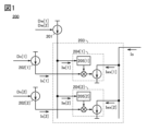
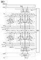
- FIG. 1 is a diagram illustrating a configuration example of a semiconductor device.
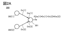
- FIGS. 2A and 2B are diagrams illustrating a configuration example of an arithmetic processing device.
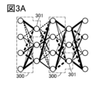
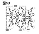
- 3A to 3C are diagrams illustrating neural networks.
- FIG. 4 is a diagram illustrating a configuration example of the arithmetic processing device.
- FIG. 5 is a block diagram showing a configuration example of a semiconductor device.
- FIGS. 6A to 6C are block diagrams showing configuration examples of circuits included in a semiconductor device.
- FIGS. 7A to 7D are circuit diagrams showing configuration examples of circuits included in a semiconductor device.
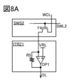
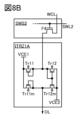
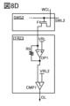
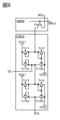
- FIGS. 8A to 8D are circuit diagrams showing configuration examples of circuits included in a semiconductor device.
- FIG. 9 is a circuit diagram showing a configuration example of a circuit included in a semiconductor device.
- FIG. 10 is a block diagram showing a configuration example of a semiconductor device.
- FIG. 11 is a block diagram showing a configuration example of a semiconductor device.
- FIG. 12 is a timing chart showing an example of the operation of the semiconductor device.
- FIG. 13 is a block diagram showing a configuration example of a semiconductor device.
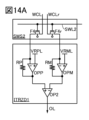
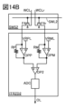
- 14A to 14C are block diagrams illustrating configuration examples of circuits included in a semiconductor device.
- FIG. 15 is a block diagram showing a configuration example of a circuit included in a semiconductor device.
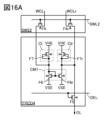
- FIG. 16A is a circuit diagram showing a configuration example of a circuit included in a semiconductor device.
- FIG. 16A is a circuit diagram showing a configuration example of a circuit included in a semiconductor device.
- 16B is a block diagram showing a configuration example of a circuit included in a semiconductor device.
- 17A and 17B are block diagrams illustrating an example of the configuration of a circuit included in a semiconductor device.
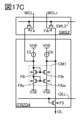
- FIG. 17C is a circuit diagram showing a configuration example of a circuit included in the semiconductor device.
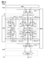
- FIG. 18 is a block diagram showing a configuration example of a semiconductor device.
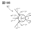
- FIGS. 19A and 19B are diagrams illustrating a hierarchical neural network.
- FIG. 20 is a block diagram showing a configuration example of a semiconductor device.
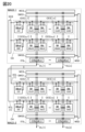
- FIG. 21 is a block diagram showing a configuration example of a semiconductor device.
- FIG. 22 is a block diagram showing a configuration example of a semiconductor device.
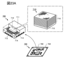
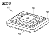
- 23A and 23B are diagrams showing an example of an electronic component.
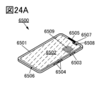
- FIGS. 24A and 24B are diagrams illustrating an example of an electronic device.
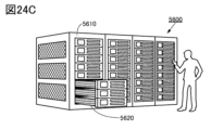
- FIGS. 24C to 24E are diagrams showing an example of a large-sized computer.
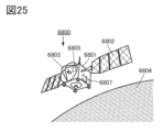
- FIG. 25 is a diagram showing an example of space equipment.
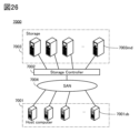
- FIG. 26 is a diagram illustrating an example of a storage system applicable to a data center.
- a semiconductor device is a device that utilizes semiconductor characteristics, and refers to, for example, a circuit including a semiconductor element (eg, a transistor, a diode, etc.), or a device having the same circuit. It also refers to any device that can function by utilizing the characteristics of semiconductors. For example, an integrated circuit including a semiconductor element, a chip including an integrated circuit, an electronic component in which a chip is housed in a package, or an electronic device in which an electronic component is mounted are examples of semiconductor devices.
- a display device may itself be a semiconductor device, and may include a semiconductor device.
- each embodiment can be appropriately combined with the structure shown in other embodiments to form one embodiment of the present invention. Further, when a plurality of configurations are shown in one embodiment, it is possible to combine these configurations as appropriate to form one aspect of the present invention.
- the size, layer thickness, or region may be exaggerated for clarity.
- the drawings are not limited, eg, in size or aspect ratio.
- the drawings schematically show ideal examples, and are not limited to, for example, the shapes or values shown in the drawings.
- a layer or a resist mask may be unintentionally reduced due to a process such as etching, but this may not be reflected in the drawings to make it easier to understand.
- variations in voltage or current may occur due to noise or timing shifts, but these may not be reflected in the drawings in order to facilitate understanding.
- the "conducting state” or “on state” of a transistor refers to, for example, a state where the source and drain of the transistor can be considered to be electrically short-circuited, or a state where the source and drain of the transistor are considered to be electrically short-circuited, or A state in which current can flow.
- the voltage between the gate and source is higher than the threshold voltage
- the voltage between the gate and source is lower than the threshold voltage.
- non-conducting state refers to a state in which the source and drain of the transistor can be considered to be electrically disconnected.
- the voltage between the gate and source is lower than the threshold voltage, or in a p-channel transistor, the voltage between the gate and source is higher than the threshold voltage.
- the state, etc. may be referred to as a “non-conducting state", “blocking state”, or “off state”.
- the "off current" of a transistor refers to a current flowing between a source and a drain (also referred to as a drain current) when the transistor is in an off state, unless otherwise specified.
- a drain current and a current flowing between a gate and a source or drain also referred to as gate leakage current
- leakage current a current flowing between a gate and a source or drain
- Embodiment 1 A semiconductor device and an arithmetic processing device according to one embodiment of the present invention will be described with reference to the drawings. Note that the semiconductor device and the arithmetic processing device according to one embodiment of the present invention may be suitably used as part of a neural network, for example. In particular, it may be suitably used as part of a neural network whose weight has been reduced by, for example, pruning.
- FIG. 1 is a schematic diagram illustrating a configuration example of a semiconductor device 200 according to one embodiment of the present invention.
- the semiconductor device 200 shown in FIG. 1 includes a first current generation section 201, a second current generation section 202[1], a second current generation section 202[2], and a product-sum calculation section 203.
- the product-sum calculation unit 203 includes a cell 204[1] and a cell 204[2].
- the cell 204[1] includes a storage unit 205[1].
- the cell 204[2] includes a storage unit 205[2].
- the first current generating section 201 has a function of outputting a first current amount Iw[1] according to the first data Dw[1].
- the first current amount Iw[1] is proportional to the first data Dw[1] (Iw[1] ⁇ Dw[1]).
- the first current amount Iw[2] is proportional to the first data Dw[2] (Iw[2] ⁇ Dw[2]).
- the second current generation section 202[1] has a function of outputting a second current amount Ix[1] according to the second data Dx[1].
- the second current amount Ix[1] is proportional to the second data Dx[1] (Ix[1] ⁇ Dx[1]).
- the second current generation unit 202[2] has a function of outputting a second current amount Ix[2] according to the second data Dx[2].
- the second current amount Ix[2] is proportional to the second data Dx[2] (Ix[2] ⁇ Dx[2]).
- the cell 204[1] has a function of storing the first current amount Iw[1] in the storage section 205[1]. It also has a function of outputting a third current amount Iwx[1] according to the multiplication of the first current amount Iw[1] and the second current amount Ix[1].
- the third current amount Iwx[1] is proportional to the product of the first current amount Iw[1] and the second current amount Ix[1] (Iwx[1] ⁇ Iw[1] ⁇ Ix[1]) do.
- the cell 204[2] has a function of storing the first current amount Iw[2] in the storage section 205[2]. It also has a function of outputting a third current amount Iwx[2] according to the multiplication of the first current amount Iw[2] and the second current amount Ix[2].
- the third current amount Iwx[2] is proportional to the product of the first current amount Iw[2] and the second current amount Ix[2] (Iwx[2] ⁇ Iw[2] ⁇ Ix[2]) do.
- the product-sum calculation unit 203 has a function of outputting a fourth current amount Io according to the addition of the third current amount Iwx[1] and the third current amount Iwx[2].
- the fourth current amount Io is proportional to the sum of the third current amount Iwx[1] and the third current amount Iwx[2] (Io ⁇ Iwx[1]+Iwx[2]).
- the fourth current amount Io is proportional to the product sum of the first current amount (Iw[1] and Iw[2]) and the second current amount (Ix[1] and Ix[2]) (Io ⁇ Iw [1] ⁇ Ix[1]+Iw[2] ⁇ Ix[2]).
- the semiconductor device 200 inputs the second data (Dx[1] and Dx[2]) and the first data (Dw[1] and Dw[1] and It has a function of outputting a fourth current amount Io according to the product-sum calculation of Dw[2]).
- the second current generation section 202[1] and the second current generation section 202[2] generate the second current amount (Ix[2]) according to the second data (Dx[1] and Dx[2]). 1] and Ix[2]), but the configuration is not limited thereto.
- a configuration may be adopted in which the second current amount (Ix[1] and Ix[2]) is directly input as the second data without providing the second current generation section.
- the present invention is not limited to this.
- an operation corresponding to an arbitrary function may be performed on the fourth current amount Io and the result may be output.
- the function include nonlinear functions such as a sigmoid function, a tanh function, a softmax function, a ReLU function, and a threshold function.
- the second current amount Ix[1] when the second data Dx[1] is zero and the second current amount Ix[2] when the second data Dx[2] is zero are each a data zero current. Suppose it is a quantity.
- the data zero current amount is the off-state current (when the transistor is in an OFF state) of the transistors constituting each of the first current generation section 201, the second current generation section 202[1], and the second current generation section 202[2].
- the current that flows between the source and drain when Therefore, the data zero current amount is, for example, 1 ⁇ 10 ⁇ 11 A or less, preferably 1 ⁇ 10 ⁇ 15 A or less, and more preferably 1 ⁇ 10 ⁇ 18 A or less.
- Each of the first current generation section 201, the second current generation section 202[1], and the second current generation section 202[2] includes, for example, a switch for controlling whether or not to output current. It is equipped with a transistor that functions as a. That is, the value of the off-state current that flows when the transistor is turned off becomes the data zero current amount.
- the transistor include a Si transistor (a transistor whose channel formation region contains silicon), an OS transistor (a transistor whose channel formation region contains an oxide semiconductor), and the like.
- An OS transistor has an extremely low off-state current because the band gap of an oxide semiconductor in which a channel is formed is 2 eV or more.
- the off-state current value of the OS transistor per 1 ⁇ m channel width at room temperature is 1aA (1 ⁇ 10 ⁇ 18 A) or less, 1zA (1 ⁇ 10 ⁇ 21 A) or less, or 1yA (1 ⁇ 10 ⁇ 24 A) or less It can be done.
- the off-state current value per 1 ⁇ m of channel width at room temperature is 1 fA (1 ⁇ 10 ⁇ 15 A) or more and 1 pA (1 ⁇ 10 ⁇ 12 A) or less. Therefore, it can be said that the off-state current of an OS transistor is about 10 orders of magnitude lower than that of a Si transistor.
- the off-state current of the OS transistor hardly increases even in a high temperature environment. Specifically, the off-state current hardly increases even under an environmental temperature of room temperature or higher and 200° C. or lower. Furthermore, the on-state current of the OS transistor does not easily decrease even in a high-temperature environment.
- the on-state current of a Si transistor decreases in a high-temperature environment. That is, an OS transistor has a higher on-state current than a Si transistor in a high-temperature environment. Furthermore, the OS transistor can perform a good switching operation even under an environmental temperature of 125° C. or higher and 150° C. or lower because it has a large ratio of on-current to off-current. Therefore, a semiconductor device including an OS transistor operates stably even in a high-temperature environment and has high reliability.
- the semiconductor layer of the OS transistor contains at least one of indium and zinc.
- the semiconductor layer of the OS transistor is made of, for example, indium, M (M is gallium, aluminum, silicon, boron, yttrium, tin, copper, vanadium, beryllium, titanium, iron, nickel, germanium, zirconium, molybdenum, lanthanum). , cerium, neodymium, hafnium, tantalum, tungsten, cobalt, magnesium, and antimony), and zinc.
- M is preferably one or more selected from gallium, aluminum, yttrium, and tin.
- an oxide containing indium (In), gallium (Ga), and zinc (Zn) also referred to as "IGZO”
- an oxide containing indium (In), aluminum (Al), and zinc (Zn) also referred to as "IAZO”
- an oxide containing indium (In), aluminum (Al), gallium (Ga), and zinc (Zn) also referred to as "IAGZO”
- IAGZO oxide containing indium (In), aluminum (Al), gallium (Ga), and zinc (Zn)
- the atomic ratio of In in the In-M-Zn oxide is preferably equal to or higher than the atomic ratio of M.
- the atomic ratio of In in the In-M-Zn oxide may be smaller than the atomic ratio of M.
- the nearby composition includes a range of plus or minus 30% of the desired atomic ratio.
- the first current generation unit 201 can generate a first current amount Iw[1] when the first data Dw[1] is zero, and a first current amount Iw[1] when the first data Dw[2] is zero. Since the first current amount Iw[2] can be made extremely small, power consumption can be reduced. Furthermore, by using an OS transistor, the second current generation unit 202[1] can make the second current amount Ix[1] extremely small when the second data Dx[1] is zero. It is possible to reduce power consumption. Furthermore, by using an OS transistor, the second current generating section 202[2] can make the second current amount Ix[2] extremely small when the second data Dx[2] is zero. It is possible to reduce power consumption.
- Each of the first current generation section 201, the second current generation section 202[1], and the second current generation section 202[2] includes, for example, a plurality of current sources, and outputs a current for each current source. By controlling whether or not to do so, it is possible to generate an amount of current according to the data. At this time, the amount of current output by one current source corresponds to the least significant bit (LSB: Least Significant Bit) of the data. Therefore, the smaller the amount of current output by one current source, the more power consumption can be reduced. Therefore, the amount of current output by one current source is, for example, 1.0 ⁇ 10 ⁇ 8 A or less, preferably 1.0 ⁇ 10 ⁇ 12 A or less, and more preferably 1.0 ⁇ 10 ⁇ 15 It is good if it is below A.
- LSB least Significant Bit
- the data zero current amount described above is, for example, two orders of magnitude lower than the current amount corresponding to the least significant bit, preferably three orders of magnitude lower, and more preferably four orders of magnitude lower. It may be the amount of current.
- each of the first current generation section 201, the second current generation section 202[1], and the second current generation section 202[2] is a current source in order to generate a current amount according to data. It is equipped with a transistor that functions as a.
- the transistor may operate, for example, in a subthreshold region (a region where the gate-source voltage of the transistor is lower than the threshold voltage and the drain current changes exponentially with respect to the gate-source voltage). That is, when the threshold voltage is within an appropriate range, the transistor can flow a current in a wide current range when operating in the subthreshold region.
- Examples of the transistor include a Si transistor or an OS transistor.
- Each of the storage section 205[1] and the storage section 205[2] can be configured with, for example, one transistor and one capacitor.
- data voltage value corresponding to the amount of current
- the first current generation section 201 corresponds to a circuit WCS described later.
- the second current generation section 202[1] and the second current generation section 202[2] correspond to a circuit XCS described later.
- the product-sum calculation unit 203 corresponds to a cell array CA described later.
- One aspect of the present invention may be configured to perform a product-sum operation on three or more first data and three or more second data.
- the semiconductor device 200 includes a first current generating section 201, a second current generating section 202[1] to a second current generating section 202[N] (where N is an integer of 2 or more). ) and a sum-of-products calculation unit 203.
- the first current generation unit 201 generates the first current amount Iw[1] to the first current amount Iw[ according to the first data Dw[1] to the first data Dw[N], respectively. N]. Further, each of the second current generation section 202[1] to second current generation section 202[N] generates a second current amount according to each of the second data Dx[1] to second data Dx[N]. It has a function of outputting each of Ix[1] to second current amount Ix[N]. Further, the sum-of-products calculation unit 203 calculates the sum of products (Iw[1] ⁇ It has a function of outputting a fourth current amount Io according to the sum of Ix[1] to Iw[N] ⁇ Ix[N].
- the semiconductor device 200 uses the input second data (Dx[1] to Dx[N]) and the second data stored in the cells 204[1] to 204[N] included in the product-sum calculation unit 203. 1 data (Dw[1] to Dw[N]), and has a function of outputting a fourth current amount Io according to a product-sum operation.
- FIG. 2A is a schematic diagram illustrating a configuration example of an arithmetic processing device 300 according to one aspect of the present invention.
- the arithmetic processing device 300 shown in FIG. 2A includes a semiconductor device 301, a semiconductor device 302[1], and a semiconductor device 302[2].
- the semiconductor device 200 described above can be applied to each of the semiconductor device 301, the semiconductor device 302[1], and the semiconductor device 302[2].
- the output of the semiconductor device 302[1] is input to the semiconductor device 301 (indicated by a solid arrow in the figure).
- data corresponding to the fourth current amount Io in the semiconductor device 302[1] (data obtained by performing an operation corresponding to an arbitrary function on the fourth current amount Io) is the second data Dx in the semiconductor device 301. It is input as [1].
- the output of the semiconductor device 302[2] is input to the semiconductor device 301 (indicated by a solid arrow in the figure).
- data corresponding to the fourth current amount Io in the semiconductor device 302[2] (data obtained by performing an operation corresponding to an arbitrary function on the fourth current amount Io) is the second data Dx in the semiconductor device 301. It is input as [2].
- the semiconductor device 301 calculates the sum of products of the input second data (Dx[1] and Dx[2]) and the first data (Dw[1] and Dw[2]) stored in the semiconductor device 301. Outputs data according to the calculation. For example, for the product-sum operation, an operation corresponding to an arbitrary function is performed, and f(Dw[1] ⁇ Dx[1]+Dw[2] ⁇ Dx[2]) is output.
- the arithmetic processing device 300 can have a stacked structure.
- a structure can be adopted in which a layer provided with the semiconductor device 301 and a layer provided with the semiconductor device 302[1] and the semiconductor device 302[2] are stacked.
- the description of Embodiment 5, which will be described later, can be referred to.
- the outputs of the semiconductor device 302[1] and the semiconductor device 302[2] are input to the semiconductor device 301 .
- the outputs of each of the semiconductor devices 302[1] to 302[N] are input to the semiconductor device 301. It may also be a configuration. That is, the arithmetic processing device 300 may include a semiconductor device 301 and semiconductor devices 302[1] to 302[N].
- the semiconductor device 301 inputs the second data (Dx[1] to Dx[N]) and the first data (Dw[1] to Dw[N] stored in the semiconductor device 301). ]) Outputs data according to the product-sum operation. For example, for the product-sum operation, an operation corresponding to an arbitrary function is performed, and f (the sum of Dw[1] ⁇ Dx[1] to Dw[N] ⁇ Dx[N]) is output.
- the arithmetic processing device 300 can constitute part of a neural network. Note that for the configuration example of the neural network, the description of Embodiment 4, which will be described later, can be referred to.
- the neural network configured by the arithmetic processing device 300 has a function of reducing at least one of the first data Dw[1] and the first data Dw[2] in the semiconductor device 301 to zero by pruning.
- At least one of the first data Dw[1] and the first data Dw[2] corresponding to the pruned net is It is zero.
- FIG. 2B is a schematic diagram showing a case where, for example, a net between the semiconductor device 301 and the semiconductor device 302[1] is cut out by pruning in the neural network configured by the arithmetic processing device 300.
- the neural network by setting the first data corresponding to the net cut by pruning to zero, the first current amount corresponding to the first data becomes the data zero current amount. Therefore, the multiplication of the term corresponding to the first data is zero, and the power consumption associated with the multiplication can be reduced to almost zero. In other words, multiplication by zero can be performed with almost zero power consumption without deleting the cut net or providing a separate circuit to determine that the data is zero. Therefore, the power consumption of the neural network configured by the arithmetic processing device 300 can be reduced.
- the neural network configured by the arithmetic processing device 300 is It has a function of setting at least one of the first data Dw[1] to first data Dw[N] in the semiconductor device 301 to zero.
- 3A to 3C are schematic diagrams illustrating an example of reducing the weight of a neural network model.
- An example of applying a lightweight neural network model to the arithmetic processing device 300 of one embodiment of the present invention will be described with reference to FIGS. 3A to 3C.
- the neural network is configured by a plurality of arithmetic processing units 300 (two are representatively numbered in the figures).
- the polarity (positive or negative) and magnitude of weight data are represented by the line type (solid line or dotted line) and thickness of the net.
- bit reduction is performed on a general DNN (Deep Neural Network) illustrated in FIG. 3A to reduce the number of bits of weight data.
- a neural network in which the bit reduction has been implemented as illustrated in FIG. 3B (in the figure, the net in which the bit reduction has been made is shown as thinner) is obtained.
- the weight data may be reduced to 1 bit by reducing the number of bits.
- a multiplication circuit can be replaced with an addition circuit, and the circuit scale can be reduced.
- the neural network that has undergone bit reduction and pruning illustrated in FIG. 3C can be configured by appropriately setting the first data to zero in each of the plurality of arithmetic processing units 300.
- the first data becomes zero in the semiconductor device 301 included in the arithmetic processing device 300, and the first current amount corresponding to the first data also becomes the data zero current amount.
- the second data becomes zero in the semiconductor device 301 included in the arithmetic processing device 300, and the second current amount corresponding to the second data also becomes the data zero current amount.
- the power consumption in the second current generation section can be reduced to almost zero.
- the power consumption in the cell that multiplies the first data and the second data is made almost zero. be able to.
- the neural network configured by the arithmetic processing unit 300 can be pruned without deleting the net pruned by circuitry or without providing a separate circuit to determine that data is zero by zero skipping. Also, it is possible to obtain the same low power consumption effect as zero skip.
- an arbitrary function is (For example, a sigmoid function, a tanh function, a softmax function, a ReLU function, a threshold function, etc.) may be performed.
- the non-linear function optimization disclosed in Non-Patent Document 1 may be performed.
- each of the semiconductor device 301 and the semiconductor devices 302[1] to 302[N] included in the arithmetic processing device 300 is capable of multi-bit operations, as described in Embodiment 2 to be described later. It is possible. Therefore, the neural network configured by the arithmetic processing device 300 can improve inference accuracy without optimizing the nonlinear function described above. For example, it is possible to improve inference accuracy by relearning a neural network that has undergone pruning using 8-bit weight data.
- the power consumption of the arithmetic processing device 300 is calculated based on the first current amount according to the first data and the second data in each of the semiconductor device 301 and the semiconductor devices 302[1] to 302[N]. It is proportional to the multiplication of the second current amount according to . Therefore, the closer each of the first data and the second data is to zero, the lower the power consumption becomes. Therefore, the neural network configured by the arithmetic processing device 300 can reduce power consumption by, for example, distributing weight data around zero by weight attenuation.
- FIG. 4 is a schematic diagram illustrating a configuration example of an arithmetic processing device 400 according to one aspect of the present invention.
- the arithmetic processing device 400 shown in FIG. 4 includes a neural network 401 configured by a plurality of arithmetic processing devices 300 (in the figure, one is given a representative reference numeral), and a control unit 402.
- the control unit 402 reads the model of the neural network 401 that has been pruned, and applies first data Dw[ to the semiconductor device 301 included in the arithmetic processing unit 300 so that the weight data corresponding to the pruned net becomes zero. 1] to first data Dw[N]. That is, the control unit 402 has a function of setting at least one of the first data Dw[1] to first data Dw[N] in the semiconductor device 301 to zero by pruning.
- FIG. 4 shows a case where a net between the semiconductor device 301 and the semiconductor device 302 [2] is pruned by pruning (the net is deleted in the figure).
- control unit 402 may have a function of performing learning, bit reduction, pruning, zero skipping, function optimization, weight attenuation, relearning, or the like on the neural network 401, for example.
- the arithmetic processing device 400 causes the control unit 402 to set at least one of the first data Dw[1] to the first data Dw[N] to zero, so that the net cut out by pruning is not deleted in terms of circuitry.
- the effect of reducing power consumption similar to that of pruning and zero skipping can be obtained by zero skipping without providing a separate circuit for determining that data is zero.
- the semiconductor device and the arithmetic processing device are not limited to the semiconductor device and the arithmetic processing device described in this embodiment. At least a part of the configuration examples, operation examples, and drawings corresponding to these illustrated in this embodiment may be compared with other configuration examples, other operation examples, other drawings, etc. described in this specification, etc. It can be combined with other embodiments as appropriate.
- FIG. 5 shows a configuration example of an arithmetic circuit that performs a product-sum operation of first data that is positive or "0" and second data that is positive or "0".
- the arithmetic circuit MAC1 shown in FIG. 5 performs a product-sum operation of first data corresponding to the potential held in each cell and input second data, and is activated using the result of the product-sum operation.
- This is a circuit that performs function calculations.
- the first data and the second data can be, for example, analog data or multivalued data (discrete data).
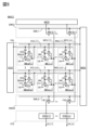
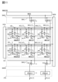
- Arithmetic circuit MAC1 includes a circuit WCS, a circuit XCS, a circuit WSD, a circuit SWS1, a circuit SWS2, a cell array CA, and a circuit ITS.
- Cell array CA includes cells IM[1,1] to cell IM[m,n] (where m is an integer greater than or equal to 1, and here n is an integer greater than or equal to 1), and cells It has IMref[1] to cell IMref[m].
- Each of the cells IM[1,1] to IM[m,n] has a function of generating and holding a potential corresponding to the amount of current according to the first data
- each of the cells IMref[1] to IMref[ m] has a function of generating and holding a potential corresponding to the amount of current according to the second data required to perform a product-sum operation with the held first data.
- each of cells IM[1,1] to cell IM[m,n] can calculate the product of the current amount according to the first data and the current amount according to the second data by giving the second data. It has the function of flowing a corresponding amount of current.
- cells IM[1,1] to IM[m,n] may be referred to as "operation cells.”
- cells IMref[1] to IMref[m] may be referred to as "drive cells”.
- the cell array CA in FIG. 5 has n+1 cells in the row direction and m cells in the column direction, arranged in a matrix, but the cell array CA has two or more cells in the row direction and one cell in the column direction. Any configuration as described above is sufficient as long as it is arranged in a matrix.
- Each of the cells IM[1,1] to IM[m,n] includes, for example, a transistor F1, a transistor F2, and a capacitor C5, and each of the cells IMref[1] to IMref[m] includes a transistor F1, a transistor F2, and a capacitor C5.
- Each includes, for example, a transistor F1m, a transistor F2m, and a capacitor C5m.
- the size (for example, channel length and channel width) and configuration of the transistors F1 included in each of cells IM[1,1] to cell IM[m,n] are equal to each other, and It is preferable that the sizes of the transistors F2 included in each of the cells IM[1,1] to IM[m,n] are equal to each other. Further, it is preferable that the sizes of the transistors F1m included in each of the cells IMref[1] to IMref[m] are the same, and the transistors F1m included in each of the cells IMref[1] to IMref[m] are preferably equal to each other. It is preferable that the sizes of F2m are equal to each other. Further, it is preferable that the transistor F1 and the transistor F1m have the same size, and it is preferable that the transistor F2 and the transistor F2m have the same size.
- each of the cells IM[1,1] to cell IM[m,n] can perform almost the same operation under the same conditions.
- the same conditions include, for example, the input potential to the source, drain, and gate of the transistor F1, the input potential to the source, drain, and gate, etc.
- the size of the transistor F1m included in each of the cells IMref[1] to IMref[m] is made equal, and the size of the transistor F2m included in each of the cells IMref[1] to IMref[m] is made equal.
- cells IMref[1] to IMref[m] can perform substantially the same operations and the results of the operations. Almost the same operation can be performed under the same conditions.
- the same conditions here include, for example, the input potential to the source, drain, and gate of the transistor F1m, the input potential to the source, drain, and gate of the transistor F2m, and the cell IMref[1] to the cell Refers to the voltage input to each of IMref[m], etc.
- each of the gate voltage, source voltage, and drain voltage of each of the transistors described above includes a case where the voltage range operates in a linear region.
- the transistor F1 and the transistor F1m may operate in a saturation region when in the on state, or may operate in a linear region and in a saturation region in a mixed manner.
- transistor F2 and transistor F2m are more preferably operated in a subthreshold region (that is, in transistor F2 or transistor F2m, when the gate-source voltage is lower than the threshold voltage). includes the case where the drain current increases exponentially with respect to the gate-source voltage. That is, each of the gate voltage, source voltage, and drain voltage of each of the transistors described above includes a case where the voltage range operates in a subthreshold region. Therefore, the transistor F2 and the transistor F2m may operate so that an off-state current flows between the source and the drain.
- the transistor F1 and the transistor F1m are OS transistors, for example.
- the channel formation regions of the transistors F1 and F1m are more preferably made of an oxide containing at least one of indium, gallium, and zinc.
- indium, element M for example, gallium, aluminum, silicon, boron, yttrium, tin, copper, vanadium, beryllium, titanium, iron, nickel, germanium, zirconium,
- An oxide containing at least one of molybdenum, lanthanum, cerium, neodymium, hafnium, tantalum, tungsten, cobalt, magnesium, and antimony may be used. .
- the off-state current of the transistor F1 and the transistor F1m can be suppressed, so that the power consumption of the arithmetic circuit can be reduced.
- the transistor F1 and the transistor F1m are in a non-conducting state, the current leaking from the holding node to the wiring WCL or the wiring XCL can be made very small, so the refresh operation of the potential of the holding node is performed. It can be reduced. Furthermore, by reducing refresh operations, power consumption of the arithmetic circuit can be reduced. Further, by making the current leaking from the holding node to the wiring WCL or the wiring XCL very small, the cell can hold the potential of the holding node for a long time, so that the calculation accuracy of the calculation circuit can be increased.
- OS transistors for the transistor F2 and the transistor F2m they can be operated in a wide current range in the subthreshold region, so power consumption can be reduced. Further, by using an OS transistor for the transistor F2 and the transistor F2m, the transistor F1 and the transistor F1m can be manufactured at the same time, so that the manufacturing process of the arithmetic circuit can be shortened in some cases. Further, the transistor F2 and the transistor F2m can be transistors containing silicon in a channel formation region (hereinafter referred to as Si transistors), other than OS transistors. As silicon, for example, amorphous silicon (sometimes referred to as hydrogenated amorphous silicon), microcrystalline silicon, polycrystalline silicon, single crystal silicon, or the like can be used.
- Si transistors silicon in a channel formation region
- silicon for example, amorphous silicon (sometimes referred to as hydrogenated amorphous silicon), microcrystalline silicon, polycrystalline silicon, single crystal silicon, or the like can be used.
- the first terminal of the transistor F1 is electrically connected to the gate of the transistor F2.
- a first terminal of the transistor F2 is electrically connected to the wiring VE.
- a first terminal of the capacitor C5 is electrically connected to the gate of the transistor F2.
- the first terminal of the transistor F1m is electrically connected to the gate of the transistor F2m.
- a first terminal of the transistor F2m is electrically connected to the wiring VE.
- a first terminal of the capacitor C5m is electrically connected to the gate of the transistor F2m.
- back gates are illustrated in the transistors F1, F2, F1m, and F2m, and although the connection configuration of the back gates is not illustrated, the electrical connections of the back gates are as follows. This can be determined at the design stage. For example, in a transistor having a back gate, the gate and the back gate may be electrically connected in order to increase the on-current (reduce the on-resistance) of the transistor. That is, for example, the gate and back gate of the transistor F1 may be electrically connected, or the gate and back gate of the transistor F1m may be electrically connected.
- the back gate of the transistor and an external circuit may be connected.
- a configuration may also be adopted in which wiring for electrical connection is provided and a potential is applied to the back gate of the transistor by the external circuit.
- the transistor F1 and the transistor F2 illustrated in FIG. 5 have a back gate
- the semiconductor device of one embodiment of the present invention is not limited to this.
- the transistor F1 and the transistor F2 illustrated in FIG. 5 may have a configuration without a back gate, that is, a transistor with a single gate structure. Further, some transistors may have a back gate, and some other transistors may have a back gate.
- the transistor F1 and the transistor F2 illustrated in FIG. 5 are n-channel transistors
- the semiconductor device of one embodiment of the present invention is not limited thereto.
- part or all of the transistor F1 and the transistor F2 may be replaced with p-channel transistors.
- descriptions may be made in this specification etc. as necessary so that the transistors F1 and F2 operate as desired.
- the potential applied by the wiring, the potential of the node NN, the potential of the node NNref, etc. may be changed.
- the wiring VE is connected between the first terminal and the second terminal of each transistor F2 of the cell IM[1,1], the cell IM[m,1], the cell IM[1,n], and the cell IM[m,n]. It also functions as a wiring for flowing a current between the first terminal and the second terminal of the transistor F2m of each of the cell IMref[1] and the cell IMref[m].
- the wiring VE functions as a wiring that supplies a constant potential.
- the constant potential can be, for example, a low level potential or a ground potential.
- the second terminal of the transistor F1 is electrically connected to the wiring WCL[1]
- the gate of the transistor F1 is electrically connected to the wiring WSL[1].
- the second terminal of the transistor F2 is electrically connected to the wiring WCL[1]
- the second terminal of the capacitor C5 is electrically connected to the wiring XCL[1]. Note that in FIG. 5, in the cell IM[1,1], the connection point between the first terminal of the transistor F1, the gate of the transistor F2, and the first terminal of the capacitor C5 is designated as a node NN[1,1]. .
- the second terminal of the transistor F1 is electrically connected to the wiring WCL[1]
- the gate of the transistor F1 is electrically connected to the wiring WSL[m].
- the second terminal of the transistor F2 is electrically connected to the wiring WCL[1]
- the second terminal of the capacitor C5 is electrically connected to the wiring XCL[m]. Note that in FIG. 5, in the cell IM[m,1], the connection point between the first terminal of the transistor F1, the gate of the transistor F2, and the first terminal of the capacitor C5 is set as the node NN[m,1]. .
- the second terminal of the transistor F1 is electrically connected to the wiring WCL[n]
- the gate of the transistor F1 is electrically connected to the wiring WSL[1].
- the second terminal of the transistor F2 is electrically connected to the wiring WCL[n]
- the second terminal of the capacitor C5 is electrically connected to the wiring XCL[1]. Note that in FIG. 5, in the cell IM[1,n], the connection point between the first terminal of the transistor F1, the gate of the transistor F2, and the first terminal of the capacitor C5 is set as a node NN[1,n]. .
- the second terminal of the transistor F1 is electrically connected to the wiring WCL[n]
- the gate of the transistor F1 is electrically connected to the wiring WSL[m].
- the second terminal of the transistor F2 is electrically connected to the wiring WCL[n]
- the second terminal of the capacitor C5 is electrically connected to the wiring XCL[m]. Note that in FIG. 5, in the cell IM[m,n], the connection point between the first terminal of the transistor F1, the gate of the transistor F2, and the first terminal of the capacitor C5 is set as a node NN[m,n]. .
- the second terminal of the transistor F1m is electrically connected to the wiring XCL[1]
- the gate of the transistor F1m is electrically connected to the wiring WSL[1].
- the second terminal of the transistor F2m is electrically connected to the wiring XCL[1]
- the second terminal of the capacitor C5 is electrically connected to the wiring XCL[1]. Note that in FIG. 5, in the cell IMref[1], the connection point between the first terminal of the transistor F1m, the gate of the transistor F2m, and the first terminal of the capacitor C5 is set as the node NNref[1].
- the second terminal of the transistor F1m is electrically connected to the wiring XCL[m]
- the gate of the transistor F1m is electrically connected to the wiring WSL[m].
- a second terminal of the transistor F2m is electrically connected to the wiring XCL[m]
- a second terminal of the capacitor C5 is electrically connected to the wiring XCL[m]. Note that in FIG. 5, in the cell IMref[m], the connection point between the first terminal of the transistor F1m, the gate of the transistor F2m, and the first terminal of the capacitor C5 is defined as a node NNref[m].
- nodes NN[1,1] to NN[m,n] and nodes NNref[1] to NNref[m] function as holding nodes for their respective cells.
- transistor F2 In cells IM[1,1] to IM[m,n], for example, when transistor F1 is in an on state, transistor F2 has a diode-connected configuration.
- the constant potential provided by the wiring VE is set to the ground potential (GND)
- the transistor F1 is in the on state, and a current of current amount I flows from the wiring WCL to the second terminal of the transistor F2, the gate of the transistor F2 (node NN)
- the potential of is determined according to the amount of current I. Note that the potential of the second terminal of the transistor F2 is ideally equal to the gate (node NN) of the transistor F2 since the transistor F1 is in the on state.
- the transistor F2 can cause a current amount I that corresponds to the ground potential of the first terminal of the transistor F2 and the potential of the gate (node NN) of the transistor F2 to flow between the source and drain of the transistor F2.
- a current amount I corresponds to the ground potential of the first terminal of the transistor F2 and the potential of the gate (node NN) of the transistor F2 to flow between the source and drain of the transistor F2.
- such an operation is referred to as, for example, "setting (programming) the current flowing between the source and drain of the transistor F2 of the cell IM to a current amount I.”
- the circuit SWS1 includes, for example, transistors F3[1] to F3[n].
- a first terminal of the transistor F3[1] is electrically connected to the wiring WCL[1]
- a second terminal of the transistor F3[1] is electrically connected to the circuit WCS
- a gate of the transistor F3[1] is electrically connected to the wiring WCL[1]. is electrically connected to the wiring SWL1.
- the first terminal of the transistor F3[n] is electrically connected to the wiring WCL[n]
- the second terminal of the transistor F3[n] is electrically connected to the circuit WCS
- the gate of the transistor F3[n] is electrically connected to the wiring SWL1.
- each of the transistors F3[1] to F3[n] for example, a transistor applicable to the transistor F1 or the transistor F2 can be used. In particular, it is preferable to use OS transistors as each of the transistors F3[1] to F3[n].
- the circuit SWS1 functions as a circuit that brings the circuit WCS and each of the wirings WCL[1] to WCL[n] into a conductive state or a non-conductive state.
- the circuit SWS2 includes, for example, transistors F4[1] to F4[n].
- the first terminal of the transistor F4[1] is electrically connected to the wiring WCL[1]
- the second terminal of the transistor F4[1] is electrically connected to the input terminal of the conversion circuit ITRZ[1]
- the gate of transistor F4[1] is electrically connected to wiring SWL2.
- the first terminal of the transistor F4[n] is electrically connected to the wiring WCL[n]
- the second terminal of the transistor F4[n] is electrically connected to the input terminal of the conversion circuit ITRZ[n]
- the gate of transistor F4[n] is electrically connected to wiring SWL2.
- each of the transistors F4[1] to F4[n] for example, a transistor applicable to the transistor F1 or the transistor F2 can be used. In particular, it is preferable to use OS transistors as each of the transistors F4[1] to F4[n].
- the circuit SWS2 has a function of making conductive or non-conductive between the wiring WCL[1] and the conversion circuit ITRZ[1] and between the wiring WCL[n] and the conversion circuit ITRZ[n].
- the circuit WCS has a function of supplying data to be stored in each cell of the cell array CA.
- the circuit XCS is electrically connected to the wirings XCL[1] to XCL[m].
- the circuit XCS supplies each of the cells IMref[1] to IMref[m] of the cell array CA with an amount of current according to reference data (also referred to as reference current), which will be described later, or an amount of current according to second data. It has a function to flow.
- the circuit WSD is electrically connected to the wiring WSL[1] to the wiring WSL[m].
- the circuit WSD supplies a predetermined signal to the wiring WSL[1] to the wiring WSL[m] when writing the first data to the cell IM[1,1] to the cell IM[m,n]. It has a function of selecting a row of cell array CA to which one data is to be written. In other words, wiring WSL[1] to wiring WSL[m] function as write word lines.
- the circuit WSD is electrically connected to the wiring SWL1 and the wiring SWL2, for example.
- the circuit WSD has a function of making the circuit WCS and the cell array CA into a conductive state or a non-conducting state by supplying a predetermined signal to the wiring SWL1, and a conversion circuit by supplying a predetermined signal to the wiring SWL2. It has a function of making conductive or non-conductive between ITRZ[1] to conversion circuit ITRZ[n] and the cell array CA.
- the circuit ITS includes, for example, conversion circuits ITRZ[1] to conversion circuits ITRZ[n].
- Each of the conversion circuits ITRZ[1] to ITRZ[n] includes, for example, an input terminal and an output terminal.
- the output terminal of the conversion circuit ITRZ[1] is electrically connected to the wiring OL[1]
- the output terminal of the conversion circuit ITRZ[n] is electrically connected to the wiring OL[n].
- Each of the conversion circuits ITRZ[1] to ITRZ[n] has a function of converting a current input into an input terminal into a voltage corresponding to the amount of current and outputting the voltage from an output terminal. has.
- the voltage can be, for example, an analog voltage or a digital voltage.
- each of the conversion circuits ITRZ[1] to conversion circuits ITRZ[n] may include a functional arithmetic circuit. In this case, for example, the converted voltage may be used to perform a function calculation by the calculation circuit, and the results of the calculation may be output to the wirings OL[1] to OL[n].
- a sigmoid function for example, a tanh function, a softmax function, a ReLU function, or a threshold function can be used as the above-mentioned function.
- Circuit WCS Circuit XCS>>
- circuit WCS circuit WCS
- circuit XCS circuit XCS
- FIG. 6A is a block diagram showing an example of the circuit WCS. Note that FIG. 6A also shows the circuit SWS1, the transistor F3, the wiring SWL1, and the wiring WCL in order to show the electrical connection of the circuit WCS with peripheral circuits. Further, the transistor F3 is any one of the transistors F3[1] to F3[n] included in the arithmetic circuit MAC1 in FIG. 5, and the wiring WCL is included in the arithmetic circuit MAC1 in FIG. One of the wirings WCL[1] to WCL[n].
- the circuit WCS shown in FIG. 6A includes a switch SWW, as an example.
- the first terminal of the switch SWW is electrically connected to the second terminal of the transistor F3, and the second terminal of the switch SWW is electrically connected to the wiring VINIL1.
- the wiring VINIL1 functions as a wiring that provides an initialization potential to the wiring WCL, and the initialization potential can be, for example, a ground potential (GND), a low level potential, or a high level potential.
- GND ground potential
- the switch SWW is assumed to be in an on state only when applying an initialization potential to the wiring WCL, and to be in an off state at other times.
- the switch SWW for example, an analog switch or an electric switch such as a transistor can be used.
- the transistor can have a structure similar to that of the transistor F1 and the transistor F2.
- mechanical switches may also be used.
- the circuit WCS in FIG. 6A includes, as an example, a plurality of current sources CS.
- the circuit WCS has a function of outputting the first data of K bits (2 K values) (K is an integer of 1 or more) as the amount of current, and in this case, the circuit WCS has a function of outputting the first data of K bits (2 K values) (K is an integer of 1 or more) as the amount of current.
- It has a current source CS.
- the circuit WCS has one current source CS that outputs information corresponding to the value of the first bit as a current, and has two current sources CS that outputs information corresponding to the value of the second bit as a current. It has 2K -1 current sources CS that output information corresponding to the value of the K- th bit as a current.
- each current source CS has a terminal T1 and a terminal T2.
- a terminal T1 of each current source CS is electrically connected to a second terminal of a transistor F3 included in the circuit SWS1.
- the terminal T2 of one current source CS is electrically connected to the wiring DW[1]
- each of the terminals T2 of the two current sources CS is electrically connected to the wiring DW[2]
- the terminal T2 of one current source CS is electrically connected to the wiring DW [2].
- Each of the terminals T2 of one current source CS is electrically connected to the wiring DW[K].
- the plurality of current sources CS included in the circuit WCS each have a function of outputting the same constant current IWut from the terminal T1.
- the error in the constant current I Wut output from each of the terminals T1 of the plurality of current sources CS is preferably within 10%, more preferably within 5%, and even more preferably within 1%.
- description will be given on the assumption that there is no error in the constant current I Wut output from the terminal T1 of the plurality of current sources CS included in the circuit WCS.
- Wiring DW[1] to wiring DW[K] function as wiring that transmits a control signal for outputting constant current IWut from electrically connected current source CS.
- the current source CS electrically connected to the wiring DW[1] supplies IWut to the transistor F3 as a constant current.
- the current source CS electrically connected to the wiring DW[1] does not output I Wut .
- the two current sources CS electrically connected to the wiring DW[2] supply a constant current of a total of 2I Wut to the transistor F3.
- the current source CS electrically connected to the wiring DW[2] supplies a constant current of 2I Wut in total. No output.
- the 2K -1 current sources CS electrically connected to the wiring DW[K] have a total of 2K -1 I
- the current source CS electrically connected to the wiring DW[K] is Does not output a constant current of 2 K-1 I Wut in total.
- the current flowing from one current source CS electrically connected to wiring DW[1] corresponds to the value of the 1st bit
- the current flowing from two current sources CS electrically connected to wiring DW[2] corresponds to the value of the first bit.
- the current flowing through the source CS corresponds to the value of the second bit
- the amount of current flowing through the K current sources CS electrically connected to the wiring DW[K] corresponds to the value of the K-th bit.
- I Wut flows as a constant current from the circuit WCS to the second terminal of the transistor F3 of the circuit SWS1.
- a low level potential is applied to the wiring DW[1]
- a high level potential is applied to the wiring DW[2].
- 2I Wut flows as a constant current from the circuit WCS to the second terminal of the transistor F3 of the circuit SWS1.
- a high level potential is applied to the wiring DW[1] and the wiring DW[2].
- 3I Wut flows as a constant current from the circuit WCS to the second terminal of the transistor F3 of the circuit SWS1. Further, for example, when the value of the first bit is "0" and the value of the second bit is "0", a low level potential is applied to the wiring DW[1] and the wiring DW "2". At this time, no constant current flows from the circuit WCS to the second terminal of the transistor F3 of the circuit SWS1.
- FIG. 6A shows the circuit WCS when K is an integer of 3 or more
- K when K is 1, the circuit WCS of FIG.
- the configuration may be such that the current source CS electrically connected to the current source CS is not provided.
- the circuit WCS in FIG. 6A can be configured without the current source CS electrically connected to the wiring DW[3] (not shown) to the wiring DW[K].
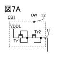
- the current source CS1 shown in FIG. 7A is a circuit that can be applied to the current source CS included in the circuit WCS of FIG. 6A, and the current source CS1 includes a transistor Tr1 and a transistor Tr2.
- the first terminal of the transistor Tr1 is electrically connected to the wiring VDDL, and the second terminal of the transistor Tr1 is electrically connected to the gate of the transistor Tr1, the back gate of the transistor Tr1, and the first terminal of the transistor Tr2. It is connected.
- the second terminal of the transistor Tr2 is electrically connected to the back gate of the transistor Tr2 and the terminal T1, and the gate of the transistor Tr2 is electrically connected to the terminal T2. Further, the terminal T2 is electrically connected to the wiring DW.
- the wiring DW is any one of the wiring DW[1] to the wiring DW[K] in FIG. 6A.
- the wiring VDDL functions as a wiring that provides a constant potential.
- the constant potential can be, for example, a high level potential.
- the high level potential is input to the first terminal of the transistor Tr1. Further, the potential of the second terminal of the transistor Tr1 is set to a potential lower than the high level potential. At this time, the first terminal of the transistor Tr1 functions as a drain, and the second terminal of the transistor Tr1 functions as a source. Further, since the gate of the transistor Tr1 and the second terminal of the transistor Tr1 are electrically connected to each other, the gate-source voltage of the transistor Tr1 is 0V. Therefore, when the threshold voltage of the transistor Tr1 is within an appropriate range, a current within the current range when operating in the subthreshold region flows between the first terminal and the second terminal of the transistor Tr1.
- the amount of the current is preferably 1.0 ⁇ 10 ⁇ 8 A or less, and more preferably 1.0 ⁇ 10 ⁇ 12 A or less, for example. , and more preferably 1.0 ⁇ 10 ⁇ 15 A or less. Further, for example, it is more preferable that the current is within a range that increases exponentially with respect to the gate-source voltage. That is, the transistor Tr1 functions as a current source for flowing a current within a current range when operating in a subthreshold region. Note that this current corresponds to I Wut described above or I Xut described later.
- Transistor Tr2 functions as a switching element.
- the first terminal of the transistor Tr2 functions as a drain, and the second terminal of the transistor Tr2 functions as a source.
- the back gate of the transistor Tr2 and the second terminal of the transistor Tr2 are electrically connected to each other, the back gate-source voltage is 0V. Therefore, when the threshold voltage of the transistor Tr2 is within an appropriate range, the transistor Tr2 is turned on by inputting a high-level potential to the gate of the transistor Tr2, and a low voltage is applied to the gate of the transistor Tr2. It is assumed that the transistor Tr2 is turned off by inputting the level potential.
- a Si transistor or an OS transistor can be used for each of the transistor Tr1 and the transistor Tr2.
- a transistor applicable to the transistor F1, the transistor F2, the transistor F3, or the transistor F4 can be used.
- the circuit applicable to the current source CS included in the circuit WCS in FIG. 6A is not limited to the current source CS1 in FIG. 7A.
- the current source CS1 has a configuration in which the back gate of the transistor Tr2 and the second terminal of the transistor Tr2 are electrically connected, but the back gate of the transistor Tr2 is electrically connected to another wiring.
- a configuration may also be used.
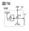
- An example of such a configuration is shown in FIG. 7B.
- the current source CS2 shown in FIG. 7B has a configuration in which the back gate of the transistor Tr2 is electrically connected to the wiring VTHL.
- the current source CS2 can apply a predetermined potential to the wiring VTHL by the external circuit, and apply the predetermined potential to the back gate of the transistor Tr2. can.
- the threshold voltage of the transistor Tr2 can be varied. In particular, by increasing the threshold voltage of the transistor Tr2, the off-state current of the transistor Tr2 can be reduced.
- the current source CS1 has a configuration in which the back gate of the transistor Tr1 and the second terminal of the transistor Tr1 are electrically connected; During this period, the voltage may be held by a capacitor.
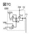
- FIG. 7C An example of such a configuration is shown in FIG. 7C.
- the current source CS3 shown in FIG. 7C includes a transistor Tr3 and a capacitor C6 in addition to the transistor Tr1 and the transistor Tr2.
- the current source CS3 is configured such that the second terminal of the transistor Tr1 and the back gate of the transistor Tr1 are electrically connected via the capacitor C6, and the back gate of the transistor Tr1 and the first terminal of the transistor Tr3 are electrically connected to each other via the capacitor C6.
- the current source CS3 has a configuration in which the second terminal of the transistor Tr3 is electrically connected to the wiring VTL, and the gate of the transistor Tr3 is electrically connected to the wiring VWL.
- the current source CS3 can bring conduction between the wiring VTL and the back gate of the transistor Tr1 by applying a high-level potential to the wiring VWL and turning on the transistor Tr3. At this time, a predetermined potential can be input from the wiring VTL to the back gate of the transistor Tr1.
- the voltage between the second terminal of the transistor Tr1 and the back gate of the transistor Tr1 can be held by the capacitor C6.
- the threshold voltage of the transistor Tr1 can be varied, and the threshold voltage of the transistor Tr1 can be fixed by the transistor Tr3 and the capacitor C6. can do.
- the current source CS4 shown in FIG. 7D may be used as a circuit that can be applied to the current source CS included in the circuit WCS of FIG. 6A.
- the current source CS4 has a configuration in which the back gate of the transistor Tr2 is electrically connected to the wiring VTHL instead of the second terminal of the transistor Tr2 in the current source CS3 of FIG. 7C. That is, like the current source CS2 in FIG. 7B, the current source CS4 can vary the threshold voltage of the transistor Tr2 depending on the potential provided by the wiring VTHL.
- the current source CS4 when a large current flows between the first terminal and the second terminal of the transistor Tr1, it is necessary to reduce the on-resistance of the transistor Tr2 in order to flow the current from the terminal T1 to the outside of the current source CS4. .
- the current source CS4 applies a high level potential to the wiring VTHL, lowers the threshold voltage of the transistor Tr2, and reduces the on-resistance of the transistor Tr2. A large current flowing between the terminals can be caused to flow from the terminal T1 to the outside of the current source CS4.
- the circuit WCS outputs a current according to the first data of K bits. can do.
- the amount of current can be, for example, the amount of current flowing between the first terminal and the second terminal within a range in which the transistor Tr1 operates in a subthreshold region.
- the circuit WCS shown in FIG. 6B may be applied.
- the circuit WCS in FIG. 6B has a configuration in which one current source CS in FIG. 7A is connected to each of the wirings DW[1] to DW[K].
- FIG. 6B shows transistor Tr1[1] and transistor Tr2[1] included in the current source WCS connected to the wiring DW[1], and transistor Tr1 included in the current source WCS connected to the wiring DW[2]. [2] and transistor Tr2[2], and transistor Tr1[K] and transistor Tr2[K] included in current source WCS connected to wiring DW[K].
- the channel width of transistor Tr1[1] is w[1]
- the channel width of transistor Tr1[2] is w[2]
- the channel width of transistor Tr1[K] is w[K]
- each of the transistor Tr1 (including the transistor Tr1[1] to the transistor Tr1[K]), the transistor Tr2 (including the transistor Tr2[1] to the transistor Tr2[K]), and the transistor Tr3 includes, for example, a Si transistor. , or an OS transistor can be used. Further, for example, a transistor applicable to the transistor F1, the transistor F2, the transistor F3, or the transistor F4 can be used.
- FIG. 6C is a block diagram showing an example of the circuit XCS. Note that FIG. 6C also shows a wiring XCL to show electrical connections between the circuit XCS and peripheral circuits. Further, the wiring XCL is any one of the wirings XCL[1] to XCL[m] included in the arithmetic circuit MAC1 in FIG.
- the circuit XCS shown in FIG. 6C includes a switch SWX, as an example.
- the first terminal of the switch SWX is electrically connected to the wiring XCL and the plurality of current sources CS, and the second terminal of the switch SWX is electrically connected to the wiring VINIL2.
- the wiring VINIL2 functions as a wiring that provides an initialization potential to the wiring XCL, and the initialization potential can be, for example, a ground potential (GND), a low level potential, or a high level potential. Further, the initialization potential given by the wiring VINIL2 may be equal to the potential given by the wiring VINIL1. Note that the switch SWX is assumed to be in an on state only when applying an initialization potential to the wiring XCL, and to be in an off state at other times.
- switch SWX for example, a switch applicable to the switch SWW can be used.
- the circuit configuration of the circuit XCS in FIG. 6C can be made substantially similar to the circuit WCS in FIG. 7A.
- the circuit XCS has a function of outputting reference data as a current amount (reference current) and a function of outputting second data of L bits (2 L value) (L is an integer of 1 or more) as a current amount. and, in this case, the circuit XCS has 2 L ⁇ 1 current sources CS.
- the circuit XCS has one current source CS that outputs information corresponding to the value of the first bit as a current, and has two current sources CS that outputs information corresponding to the value of the second bit as a current.
- it has 2 L-1 current sources CS that output information corresponding to the value of the L-th bit as a current.
- the reference data that the circuit XCS outputs as a current may be, for example, information in which the value of the first bit is "1" and the values of the second and subsequent bits are "0".
- the terminal T2 of one current source CS is electrically connected to the wiring DX[1], and each of the terminals T2 of the two current sources CS is electrically connected to the wiring DX[2], Each of the terminals T2 of the 2L -1 current sources CS is electrically connected to the wiring DX[L].
- the plurality of current sources CS included in the circuit XCS each have a function of outputting IXut from the terminal T1 as the same constant current.
- the wiring DX[1] to the wiring DX[L] function as wiring that transmits a control signal for outputting IXut from the electrically connected current source CS.
- the circuit XCS has a function of flowing the amount of current in accordance with the L-bit information sent from the wirings DX[1] to DX[L] to the wirings XCL.
- the amount of current output by the circuit XCS (for example, 0, I Xut , 2I Xut , or 3I Xut ) can be the second data output by the circuit I Xut can be the reference data output by the circuit XCS.
- the constant current I Xut output from each of the terminals T1 of the plurality of current sources CS The error is preferably within 10%, more preferably within 5%, and even more preferably within 1%. In this embodiment, description will be made on the assumption that there is no error in the constant current IXut output from the terminal T1 of the plurality of current sources CS included in the circuit XCS.
- any of the current sources CS1 to CS4 in FIGS. 7A to 7D can be applied, similarly to the current source CS of the circuit WCS.
- the wiring DW illustrated in FIGS. 7A to 7D may be replaced with the wiring DX.
- the circuit XCS can cause a current in the current range when operating in the subthreshold region to flow through the wiring XCL as reference data or L-bit second data.
- circuit XCS in FIG. 6C a circuit configuration similar to the circuit WCS shown in FIG. 6B can be applied.
- the circuit WCS shown in FIG. 6B is replaced with the circuit XCS
- the wiring DW[1] is replaced with the wiring DX[1]
- the wiring DW[2] is replaced with the wiring DX[2]
- the wiring DW[K] is replaced with the wiring DX[L]
- switch SWW may be replaced with switch SWX
- wiring VINIL1 may be replaced with wiring VINIL2.
- the conversion circuit ITRZ1 shown in FIG. 8A is an example of a circuit that can be applied to the conversion circuits ITRZ[1] to ITRZ[n] in FIG. 5. Note that FIG. 8A also shows the circuit SWS2, the wiring WCL, the wiring SWL2, and the transistor F4 in order to show the electrical connection of the conversion circuit ITRZ1 with peripheral circuits. Further, the wiring WCL is any one of the wirings WCL[1] to wiring WCL[n] included in the arithmetic circuit MAC1 in FIG. 5, and the transistor F4 is included in the arithmetic circuit MAC1 in FIG. One of transistors F4[1] to F4[n].
- the conversion circuit ITRZ1 in FIG. 8A is electrically connected to the wiring WCL via the transistor F4. Further, the conversion circuit ITRZ1 is electrically connected to the wiring OL.
- the conversion circuit ITRZ1 has a function of converting the amount of current flowing from the conversion circuit ITRZ1 to the wiring WCL or the amount of current flowing from the wiring WCL to the conversion circuit ITRZ1 into an analog voltage, and outputting the analog voltage to the wiring OL. That is, the conversion circuit ITRZ1 has a current-voltage conversion circuit.
- the conversion circuit ITRZ1 in FIG. 8A includes, as an example, a resistor R5 and an operational amplifier OP1.
- the inverting input terminal of the operational amplifier OP1 is electrically connected to the first terminal of the resistor R5 and the second terminal of the transistor F4.
- a non-inverting input terminal of the operational amplifier OP1 is electrically connected to the wiring VRL.
- the output terminal of the operational amplifier OP1 is electrically connected to the second terminal of the resistor R5 and the wiring OL.
- the wiring VRL functions as a wiring that provides a constant potential.
- the constant potential can be, for example, a ground potential (GND) or a low-level potential.
- the conversion circuit ITRZ1 can reduce the amount of current flowing from the wiring WCL to the conversion circuit ITRZ1 via the transistor F4, or the amount of current flowing from the conversion circuit ITRZ1 to the wiring WCL via the transistor F4.
- the amount can be converted into an analog voltage and output to the wiring OL.
- the inverting input terminal of the operational amplifier OP1 becomes virtual ground, so the analog voltage output to the wiring OL is based on the ground potential (GND). It can be a voltage.
- the conversion circuit ITRZ1 in FIG. 8A has a configuration that outputs an analog voltage
- the conversion circuit ITRZ[1] to conversion circuit ITRZ[n] shown in FIG. 5 may have a configuration that outputs an analog current. .
- the conversion circuit ITRZ1A shown in FIG. 8B is a circuit that causes the same amount of current to flow through the wiring OL as the analog current flowing through the wiring WCL.
- the conversion circuit ITRZ1A includes a transistor Tr11, a transistor Tr11m, a transistor Tr12, and a transistor Tr12m.
- a Si transistor or an OS transistor can be used for each of the transistor Tr11, the transistor Tr11m, the transistor Tr12, and the transistor Tr12m.
- a transistor applicable to the transistor F1, the transistor F2, the transistor F3, or the transistor F4 can be used.
- the first terminal of the transistor Tr11 is electrically connected to the wiring VCE1, and the second terminal of the transistor Tr11 is connected to the gate of the transistor Tr11, the first terminal of the transistor Tr12, the gate of the transistor Tr12, and the gate of the transistor Tr12m.
- the second terminal of the transistor F4 of the circuit SWS2 and the second terminal of the transistor Tr12 is electrically connected to the wiring VCE2.
- a first terminal of the transistor Tr11m is electrically connected to the wiring VCE1
- a second terminal of the transistor Tr11m is electrically connected to the gate of the transistor Tr11m, the first terminal of the transistor Tr12m, and the wiring OL
- the second terminal of the transistor Tr12m is electrically connected to the wiring VCE2.
- the wiring VCE1 functions as a wiring that applies a potential to each first terminal of the transistor Tr11 and the transistor Tr11m. Further, the constant potential can be, for example, a high level potential.
- the wiring VCE2 functions as a wiring that applies a potential to each second terminal of the transistor Tr12 and the transistor Tr12m.
- the constant potential can be, for example, a ground potential, a low level potential, or a negative potential.
- each of the transistor Tr11 and the transistor Tr11m a gate and a second terminal are electrically connected, and a first terminal and a wiring VCE1 that provides a high-level potential are electrically connected. Therefore, the gate-source voltage of each of the transistor Tr11 and the transistor Tr11m becomes 0V, and when the threshold voltage of each of the transistor Tr11 and the transistor Tr11m is within an appropriate range, each of the transistor Tr11 and the transistor Tr11m A current in the current range when operating in the subthreshold region flows between the first terminal and the second terminal of the device. In other words, each of the transistor Tr11 and the transistor Tr11m functions as a constant current source.
- the connection configuration of the transistor Tr12 and the transistor Tr12m is a current mirror circuit. It has become. That is, ideally, the amount of current flowing between the source and drain of the transistor Tr12 is equal to the amount of current flowing between the source and drain of the transistor Tr12m.
- the conversion circuit ITRZ1 in FIG. 8A is configured to output an analog voltage
- the conversion circuit ITRZ1A in FIG. 8B is configured to output an analog current.
- the circuit configuration applicable to the circuit ITRZ[n] is not limited to this.
- the conversion circuit ITRZ1 may have a configuration including an analog-to-digital conversion circuit ADC, as shown in FIG. 8C.
- the input terminal of the analog-to-digital conversion circuit ADC is electrically connected to the output terminal of the operational amplifier OP1 and the second terminal of the resistor R5.
- the configuration is such that the output terminal is electrically connected to the wiring OL. With such a configuration, the conversion circuit ITRZ2 in FIG. 8C can output a digital signal to the wiring OL.
- the conversion circuit ITRZ2 when the digital signal output to the wiring OL is 1 bit (binary), the conversion circuit ITRZ2 may be replaced with the conversion circuit ITRZ3 shown in FIG. 8D.
- the conversion circuit ITRZ3 in FIG. 8D has a configuration in which a comparator CMP1 is provided in the conversion circuit ITRZ1 in FIG. 8A. Specifically, in the conversion circuit ITRZ3, the first input terminal of the comparator CMP1 is electrically connected to the output terminal of the operational amplifier OP1 and the second terminal of the resistor R5, and the second input terminal of the comparator CMP1 is connected to the wiring VRL2. The output terminal of the comparator CMP1 is electrically connected to the wiring OL.
- the wiring VRL2 functions as a wiring that provides a potential for comparison with the potential of the first terminal of the comparator CMP1.
- the conversion circuit ITRZ3 in FIG. 8D can adjust the magnitude of the voltage converted from the amount of current flowing between the source and drain of the transistor F4 by the current-voltage conversion circuit and the voltage applied by the wiring VRL2.
- a low level potential or a high level potential can be output to the wiring OL depending on the output voltage.
- the conversion circuits ITRZ[1] to ITRZ[n] that can be applied to the arithmetic circuit MAC1 in FIG. 5 are not limited to the conversion circuits ITRZ1 to ITRZ3 shown in FIGS. 8A to 8D, respectively.
- the conversion circuits ITRZ1 to ITRZ3 include functional arithmetic circuits.
- the functional arithmetic circuit may be, for example, an arithmetic circuit for a sigmoid function, a tanh function, a softmax function, a ReLU function, or a threshold function.
- the conversion circuit ITRZ4 shown in FIG. 9 may be applied to the conversion circuits ITRZ[1] to ITRZ[n].
- the conversion circuit ITRZ4 is a modification of the conversion circuit ITRZ1A in FIG. 8B, and includes a transistor Tr13, a transistor Tr13m, a transistor Tr14, and a transistor in addition to the transistor Tr11, the transistor Tr11m, the transistor Tr12, and the transistor Tr12m. It has Tr14m.
- a Si transistor or an OS transistor can be used for each of the transistor Tr13, the transistor Tr13m, the transistor Tr14, and the transistor Tr14m.
- a transistor applicable to the transistor F1, the transistor F2, the transistor F3, or the transistor F4 can be used.
- the first terminal of the transistor Tr13 is electrically connected to the wiring VCE1, and the second terminal of the transistor Tr13 is connected to the gate of the transistor Tr13, the first terminal of the transistor Tr14, the gate of the transistor Tr14, and the gate of the transistor Tr14m.
- the second terminal of the transistor Tr11m, the gate of the transistor Tr11m, the first terminal of the transistor Tr12m, and the wiring ISL, and the second terminal of the transistor Tr14 is electrically connected to the wiring VCE2. ing.
- a first terminal of the transistor Tr13m is electrically connected to the wiring VCE1
- a second terminal of the transistor Tr13m is electrically connected to the gate of the transistor Tr13m, the first terminal of the transistor Tr14m, and the wiring OL
- the second terminal of the transistor Tr14m is electrically connected to the wiring VCE2.
- the transistor Tr13 and the transistor Tr13m of the conversion circuit ITRZ4 function as a constant current source like the transistor Tr11 and the transistor Tr11m
- the transistor Tr14 and the transistor Tr14m of the conversion circuit ITRZ4 function as a constant current source as well as the transistor Tr12 and the transistor Tr12m.
- it functions as a current mirror circuit.
- the wiring ISL functions as a wiring for discharging a constant current of current amount ISTD from the conversion circuit ITRZ4.
- I STD corresponds to a reference value for the ReLU function in the conversion circuit ITRZ4.
- the conversion circuit ITRZ4 When a current with a current amount I OP is output from the conversion circuit ITRZ4 to the wiring WCL, if I OP is larger than ISTD , the conversion circuit ITRZ4 outputs a current of the current amount I OP - I STD to the wiring OL. Output. Further, when I OP is less than or equal to ISTD , no current is output to the wiring OL.
- one embodiment of the present invention is not limited to the circuit configuration of the arithmetic circuit MAC1 described in this embodiment.
- the circuit configuration of the arithmetic circuit MAC1 can be changed depending on the situation.
- the arithmetic circuit MAC1 may be changed to a configuration in which the circuit SWS1 is not provided, as shown in the arithmetic circuit MAC1A shown in FIG.
- the circuit SWS1 can stop the current flowing from the circuit WCS to the wiring WCL[1] to the wiring WCL[n]
- the circuit WCS can stop the current flowing from the circuit WCS to the wiring WCL[1] to the wiring WCL[n]. It is sufficient to stop the current flowing through [1] to the wiring WCL[n].
- the arithmetic circuit MAC1 includes a transistor F2c provided between the transistor F2 and the wiring WCL in the cell IM, and a transistor F2c provided between the transistor F2m and the wiring XCL in the cell IMref.
- a transistor F2cm may be provided.
- the transistor F2c and the transistor F2cm function as a clamp transistor (sometimes referred to as a clamp FET). Therefore, it is preferable that a constant potential be applied to each gate of the transistor F2c and the transistor F2cm.
- a clamp transistor sometimes referred to as a clamp FET
- the wiring VB is electrically connected to the gates of the transistors F2c and F2cm, and as described above, it is preferable that a constant potential is applied to the wiring VB.
- DIBL drain induced barrier lowering
- a transistor applicable to each of the transistor F2 and the transistor F2m can be used.
- FIG. 12 shows a timing chart of an example of the operation of the arithmetic circuit MAC1.
- the timing chart in FIG. 12 shows wiring SWL1, wiring SWL2, wiring WSL[i] (i is an integer from 1 to m-1), and wiring from time T11 to time T23 and in the vicinity thereof.
- arbitrary cells are defined as cell IM[i,1], cell IM[i,j], cell IM[i,n], cell IM[i+1, 1], cell IM[i+1,j], or cell IM[i+1,n].
- i is an integer from 1 to m
- j is an integer from 1 to n.
- it is expressed as a cell IMref[i], a cell IMref[i+1], or the like.
- nodes NN in any cell are expressed as nodes NN[i,1], nodes NN[i,n], nodes NN[i+1,1], nodes NN[i+1,n], and so on.
- an arbitrary conversion circuit ITRZ is expressed as a conversion circuit ITRZ[j] or the like.
- circuit WCS of FIG. 6A is applied as the circuit WCS of the arithmetic circuit MAC1
- the circuit XCS of FIG. 6C is applied as the circuit XCS of the arithmetic circuit MAC1.
- the potential of the wiring VE is set to the ground potential GND.
- the potentials of nodes NN[i,j], nodes NN[i+1,j], nodes NNref[i], and nodes NNref[i+1] are set to the ground potential GND. It is assumed that Specifically, for example, the potential for initializing the wiring VINIL1 in FIG. By turning on each transistor F1, the potentials of the nodes NN[i,j] and NN[i+1,j] can be set to the ground potential GND. Further, for example, the initialization potential of the wiring VINIL2 in FIG.
- a high level potential (denoted as High in FIG. 12) is applied to the wiring SWL1
- a low level potential (denoted as Low in FIG. 12) is applied to the wiring SWL2.
- a high level potential is applied to the gates of each of the transistors F3[1] to F3[n]
- each of the transistors F3[1] to F3[n] is turned on
- the transistor F4[1] A low level potential is applied to the gates of each of the transistors F4[n] to turn off each of the transistors F4[1] to F4[n].
- a low level potential is applied to the wiring WSL[i] and the wiring WSL[i+1].
- the gate of the transistor F1 included in the i-th cell IM[i,1] to cell IM[i,n] of the cell array CA and the gate of the transistor F1m included in the cell IMref[i] A low level potential is applied to and, and the respective transistors F1 and F1m are turned off.
- the gate of the transistor F1 included in the i+1th row cell IM[i+1,1] to cell IM[i+1,n] of the cell array CA, and the gate of the transistor F1m included in the cell IMref[i+1] a low level potential is applied to the transistors F1 and F1m, respectively, and the transistors F1 and F1m are turned off.
- the ground potential GND is applied to the wiring XCL[i] and the wiring XCL[i+1].
- the initialization potential of the wiring VINIL2 is set to the ground potential GND, and the switch SWX By turning on, the potentials of the wiring XCL[i] and the wiring XCL[i+1] can be set to the ground potential GND.
- a high-level potential is applied to the wiring WSL[i] between time T12 and time T13.
- the gate of the transistor F1 included in the i-th cell IM[i,1] to cell IM[i,n] of the cell array CA and the gate of the transistor F1m included in the cell IMref[i] A high level potential is applied to and, and the respective transistors F1 and F1m are turned on.
- a low level potential is applied to the wiring WSL[1] to wiring WSL[m] except for the wiring WSL[i], and the cells other than the i-th row of the cell array CA
- the transistor F1 included in IM[1,1] to cell IM[m,n] and the transistor F1m included in cell IMref[1] to cell IMref[m] other than the i-th row are as follows. Assume that it is in the off state.
- ground potential GND has been continuously applied to the wirings XCL[1] to XCL[m] since before time T12.
- a current of current amount I 0 [i, j] flows from the circuit WCS to the cell array CA via the transistor F3 [j] as the first data.
- the wiring WCL shown in FIG. 6A is the wiring WCL[j]
- a current I 0 [i,j] flows from the circuit WCS to the second terminal of the transistor F3[j].
- the transistor F2 included in the cell IM[i,j] has a diode-connected configuration. Therefore, when a current flows from the wiring WCL[j] to the cell IM[i,j], the potentials of the gate of the transistor F2 and the second terminal of the transistor F2 become approximately equal.
- the potential is determined, for example, by the amount of current flowing from the wiring WCL[j] to the cell IM[i,j], the potential of the first terminal of the transistor F2 (here, GND), and the like.
- the threshold voltage of transistor F2 is V th [i, j]
- the amount of current I 0 [i, j] when transistor F2 operates in the subthreshold region is written as the following formula. can.
- I a is the drain current when V g [i, j] is V th [i, j], and J is a correction coefficient determined by, for example, temperature and device structure.
- a current of current amount I ref0 flows from the circuit XCS to the wiring XCL[i] as reference data.
- the wiring XCL shown in FIG. 6C is the wiring XCL[i]
- the wiring DX[1] has a high level potential
- each of the wirings DX[2] to DX[L] has a low level potential.
- I ref0 I Xut .
- transistor F1m included in cell IMref[i] is turned on, and transistor F2m included in cell IMref[i] has a diode-connected configuration. . Therefore, when a current flows from the wiring XCL[i] to the cell IMref[i], the potentials of the gate of the transistor F2m and the second terminal of the transistor F2m become approximately equal.
- the potential is determined by, for example, the amount of current flowing from the wiring XCL[i] to the cell IMref[i], the potential of the first terminal of the transistor F2m (here, GND), and the like.
- the gate of the transistor F2m (node NNref[i]) becomes V gm [i] due to a current of current amount I ref0 flowing from the wiring XCL[i] to the cell IMref[i]. Furthermore, the potential of the wiring XCL[i] at this time is also assumed to be V gm [i]. That is, in the transistor F2m, the gate-source voltage becomes V gm [i] - GND, and the current amount I ref0 is set as the current flowing between the first terminal and the second terminal of the transistor F2m.
- the amount of current I ref0 when the transistor F2m operates in the subthreshold region can be described as follows.
- the correction coefficient J is the same as that of the transistor F2 included in the cell IM[i,j].
- the transistors have the same device structure and size (channel length and channel width).
- the correction coefficient J of each transistor varies due to manufacturing variations, but it is assumed that the variations are suppressed to the extent that the discussion described below holds with sufficient accuracy for practical use.
- the first data w[i,j] is defined as follows.
- equation (1.1) can be rewritten as the following formula:
- a low-level potential is applied to the wiring WSL[i] between time T14 and time T15.
- the gate of the transistor F1 included in the i-th cell IM[i,1] to cell IM[i,n] of the cell array CA and the gate of the transistor F1m included in the cell IMref[i] A low level potential is applied to and, and the respective transistors F1 and F1m are turned off.
- the transistor F1 included in the cell IM[i,j] When the transistor F1 included in the cell IM[i,j] is turned off, the potential of the gate of the transistor F2 (node NN[i,j]) and the potential of the wiring XCL[i] are stored in the capacitor C5. The difference between the potential and the potential, V g [i, j] - V gm [i], is held. Furthermore, since the transistor F1m included in the cell IMref[i] is turned off, the capacitor C5m has the potential of the gate of the transistor F2m (node NNref[i]) and the potential of the wiring XCL[i]. , which is the difference between , is retained.
- the voltage held by the capacitor C5m may be a voltage other than 0 (here, for example, V ds) depending on the transistor characteristics of the transistor F1m and the transistor F2m during the operation from time T13 to time T14. be.
- the potential of the node NNref[i] may be considered as the potential of the wiring XCL[i] plus V ds .
- ⁇ From time T15 to time T16>> GND is applied to the wiring XCL[i] between time T15 and time T16.
- the wiring XCL shown in FIG. 6C is the wiring XCL[i]
- the wiring XCL[i] by setting the initialization potential of the wiring VINIL2 to the ground potential GND and turning on the switch SWX, the wiring The potential of XCL[i] can be set to the ground potential GND.
- the nodes NN[i,1] to NN[i,n] are The potential of node NNref[i] changes, and the potential of node NNref[i] changes due to capacitive coupling by capacitor C5m included in cell IMref[i].
- the amount of change in potential of nodes NN[i,1] to node NN[i,n] is equal to the amount of change in potential of wiring XCL[i] and each cell IM[i,1] included in cell array CA.
- the potential is multiplied by a capacitive coupling coefficient determined by the configuration of cells IM[i,n].
- the capacitive coupling coefficient is calculated from the capacitance of the capacitor C5, the gate capacitance of the transistor F2, and the parasitic capacitance.
- the potential of node NN[i,j] of cell IM[i,j] is as follows.
- the potential decreases by p(V gm [i]-GND) from the potential at the time between time T14 and time T15.
- the potential of the node NNref[i] also changes due to capacitive coupling by the capacitor C5m included in the cell IMref[i].
- the capacitive coupling coefficient due to the capacitor C5m is p as in the case of the capacitor C5
- a high-level potential is applied to the wiring WSL[i+1] between time T16 and time T17.
- the gates of transistors F1 included in cells IM[i+1,1] to cell IM[i+1,n] in the i+1st row of cell array CA and the gates of transistors F1m included in cell IMref[i+1] A high level potential is applied to and, and the respective transistors F1 and F1m are turned on.
- a low level potential is applied to the wiring WSL[1] to wiring WSL[m] except for the wiring WSL[i+1], and the cells other than the i+1th row of the cell array CA
- the transistor F1 included in IM[1,1] to cell IM[m,n] and the transistor F1m included in cell IMref[1] to cell IMref[m] other than the i+1th row are as follows. Assume that it is in the off state.
- ground potential GND has been continuously applied to the wirings XCL[1] to XCL[m] since before time T16.
- a current of current amount I 0 [i+1,j] flows from the circuit WCS to the cell array CA via the transistor F3[j] as the first data.
- the wiring WCL shown in FIG. 6A is the wiring WCL[j+1]
- a current I 0 [i+1,j] flows from the circuit WCS to the second terminal of the transistor F3[j].
- the transistor F2 included in the cell IM[i+1,j] has a diode-connected configuration. Therefore, when a current flows from the wiring WCL[j] to the cell IM[i+1,j], the potentials of the gate of the transistor F2 and the second terminal of the transistor F2 become approximately equal.
- the potential is determined by, for example, the amount of current flowing from the wiring WCL[j] to the cell IM[i+1,j], the potential of the first terminal of the transistor F2 (here, GND), and the like.
- a current amount I 0 [i+1,j] flows from the wiring WCL[j] to the cell IM[i+1,j], so that the potential of the gate of the transistor F2 (node NN[i+1,j]) is assumed to be V g [i+1,j]. That is, in the transistor F2, the gate-source voltage becomes V g [i+1,j]-GND, and the current amount I 0 [i+1,j] is set as the current flowing between the first terminal and the second terminal of the transistor F2. be done.
- the threshold voltage of transistor F2 is V th [i+1, j]
- the amount of current I 0 [i+1, j] when transistor F2 operates in the subthreshold region is written as the following formula. can.
- the correction coefficient is J, which is the same as the transistor F2 included in the cell IM[i,j] and the transistor F2m included in the cell IMref[i].
- a current of current amount I ref0 flows from the circuit XCS to the wiring XCL[i+1] as reference data.
- the wiring DX[1] has a high level potential
- the wiring DX[2] A low level potential is input to each of the wirings DX[L] to DX[L]
- the transistor F2m included in the cell IMref[i+1,j] has a diode-connected configuration. becomes. Therefore, when a current flows from the wiring XCL[i+1] to the cell IMref[i+1], the potentials of the gate of the transistor F2m and the second terminal of the transistor F2m are approximately equal.
- the potential is determined, for example, by the amount of current flowing from the wiring XCL[i+1] to the cell IMref[i+1], the potential of the first terminal of the transistor F2m (here, GND), and the like.
- the gate of the transistor F2m (node NNref[i+1]) becomes V gm [i+1] due to a current amount I ref0 flowing from the wiring XCL[i+1] to the cell IMref[i+1], Furthermore, the potential of the wiring XCL[i+1] at this time is also assumed to be V gm [i+1]. That is, in the transistor F2m, the gate-source voltage becomes V gm [i+1] - GND, and the current amount I ref0 is set as the current flowing between the first terminal and the second terminal of the transistor F2m.
- the threshold voltage of the transistor F2m is V thm [i+1,j]
- the amount of current I ref0 when the transistor F2m operates in the subthreshold region can be described as follows.
- the correction coefficient J is the same as that of the transistor F2 included in the cell IM[i+1,j].
- the first data w[i+1,j] is defined as follows.
- a low level potential is applied to the wiring WSL[i+1] between time T18 and time T19.
- the gates of transistors F1 included in cells IM[i+1,1] to cell IM[i+1,n] in the i+1st row of cell array CA and the gates of transistors F1m included in cell IMref[i+1] A low level potential is applied to and, and the respective transistors F1 and F1m are turned off.
- the transistor F1 included in the cell IM[i+1,j] When the transistor F1 included in the cell IM[i+1,j] is turned off, the potential of the gate of the transistor F2 (node NN[i+1,j]) and the potential of the wiring XCL[i+1] are stored in the capacitor C5. The difference between the potential and the potential, V g [i+1,j] ⁇ V gm [i+1], is held. Furthermore, since the transistor F1m included in the cell IMref[i+1] is turned off, the capacitor C5m has the potential of the gate of the transistor F2m (node NNref[i+1]) and the potential of the wiring XCL[i+1]. , which is the difference between , is retained.
- the voltage held by the capacitor C5m may be a voltage other than 0 (here, for example, V ds) depending on the transistor characteristics of the transistor F1m and the transistor F2m during the operation from time T18 to time T19. be.
- the potential of the node NNref[i+1] may be considered as the potential of the wiring XCL[i+1] plus V ds .
- ground potential GND is applied to wiring XCL[i+1].
- the wiring XCL shown in FIG. 6C is the wiring XCL[i+1]
- the wiring The potential of XCL[i+1] can be set to the ground potential GND.
- the nodes NN[i+1,1] to NN[i+1,n] The potential of the node NNref[i+1] changes due to capacitive coupling due to the capacitor C5m included in the cell IMref[i+1].
- the amount of change in potential of nodes NN[i+1,1] to node NN[i+1,n] is equal to the amount of change in potential of wiring XCL[i+1] and each cell IM[i+1,1] included in cell array CA.
- the potential is multiplied by a capacitive coupling coefficient determined by the configuration of cells IM[i+1,n].
- the capacitive coupling coefficient is calculated from, for example, the capacitance of the capacitor C5, the gate capacitance of the transistor F2, the parasitic capacitance, and the like.
- the capacitive coupling coefficient due to capacitor C5 is calculated as the capacitive coupling coefficient due to capacitor C5 in each of cell IM[i,1] to cell IM[i,n]. Similar to the coefficient, when p is the potential of the node NN[i+1,j] of the cell IM[i+1,j], from the potential between time T18 and time T19, p(V gm [i+1] -GND) decreases.
- the potential of the node NNref[i+1] also changes due to capacitive coupling by the capacitor C5m included in the cell IMref[i+1].
- the capacitive coupling coefficient due to the capacitor C5m is p as in the case of the capacitor C5
- the potential of the node NNref[i+1] of the cell IMref[i+1] is changed from the potential between time T18 and time T19 to p(V gm [ i+1]-GND) decreases.
- p 1 as an example. Therefore, the potential of the node NNref[i+1] from time T20 to time T21 becomes GND.
- a low level potential is applied to the wiring SWL1 from time T20 to time T21.
- a low level potential is applied to the gates of each of the transistors F3[1] to F3[n], and each of the transistors F3[1] to F3[n] is turned off.
- a high-level potential is applied to the wiring SWL2 between time T21 and time T22.
- a high level potential is applied to the gates of each of the transistors F4[1] to F4[n], and each of the transistors F4[1] to F4[n] is turned on.
- a current of x[i]I ref0 which is x[i] times the current amount I ref0 , flows from the circuit XCS to the wiring XCL[i] as second data. That is, the current flowing from the circuit XCS to the wiring XCL[i] is changed from the current amount I ref0 to the current amount x[i]I ref0 .
- the potential of the node NNref[i] changes due to capacitive coupling by the capacitor C5m included in the cell IMref[i]. Therefore, the potential of the node NNref[i] of the cell IMref[i] becomes V gm [i]+p ⁇ V[i].
- the amount of current I 1 [i,j] flowing between the first terminal and the second terminal of the transistor F2 and the amount of current flowing between the first terminal and the second terminal of the transistor F2m The current amount I ref1 [i, j] can be described as follows.
- the amount of current flowing between the first terminal and the second terminal of the transistor F2 included in the cell IM[i,j] is based on the first data w[i,j], the second data x[i], , is proportional to the product of .
- a current of x[i+1]I ref0 flows from the circuit XCS to the wiring XCL [i+1] as second data. That is, the current flowing from the circuit XCS to the wiring XCL[i+1] is changed from the current amount I ref0 to the current amount x[i+1]I ref0 .
- equation (1.13) can be rewritten as the following equation.
- the amount of current flowing between the first and second terminals of the transistor F2 included in the cell IM[i+1,j] is based on the first data w[i+1,j] and the second data x It is proportional to the product of [i+1].
- I S [j] I S [j] can be expressed by the following equation from equation (1.12) and equation (1.16).
- the amount of current output from the conversion circuit ITRZ[j] is determined by the first data w[i,j] and w[i+1,j] and the second data x[i] and x[i+1]
- the amount of current is proportional to the sum of the products of and.
- the arithmetic circuit MAC1 having the cell array CA of three or more rows and two or more columns, the product-sum operation can be performed as described above.
- the arithmetic circuit MAC1 simultaneously performs product-sum calculation processing for the number of remaining columns among the plurality of columns by setting one column among the plurality of columns as a cell that holds I ref0 and xI ref0 as the current amount. can be executed.
- the arithmetic circuit MAC1 simultaneously performs product-sum calculation processing for the number of remaining columns among the plurality of columns by setting one column among the plurality of columns as a cell that holds I ref0 and xI ref0 as the current amount.
- the operation example of the arithmetic circuit MAC1 described above is suitable for calculating the sum of products of positive first data and positive second data.
- an operation example of calculating the sum of products of positive or negative first data and positive second data, and also calculating the sum of products of positive or negative first data and positive or negative second data is suitable for calculating the sum of products of positive first data and positive second data.
- An example of the calculation operation will be described in the third embodiment.
- the transistor included in the arithmetic circuit MAC1 is an OS transistor or a Si transistor; however, one embodiment of the present invention is not limited thereto.
- the transistors included in the arithmetic circuit MAC1 are, for example, transistors whose channel formation regions contain Ge or the like, transistors whose channel formation regions contain compound semiconductors such as ZnSe, CdS, GaAs, InP, GaN, or SiGe, and transistors whose channel formation regions contain Ge or the like.
- a transistor in which a nanotube is included in a channel formation region, a transistor in which an organic semiconductor is included in a channel formation region, or the like can be used.
- FIG. 13 shows a configuration example of an arithmetic circuit that performs a product-sum operation of first data that is positive, negative, or "0" and second data that is positive or "0."
- the arithmetic circuit MAC2 shown in FIG. 13 has a configuration that is a modification of the arithmetic circuit MAC1 shown in FIG. Therefore, in the explanation of the arithmetic circuit MAC2, parts that overlap with the explanation of the arithmetic circuit MAC1 will be omitted.
- the cell array CA shown in FIG. 13 has circuits CES[1,j] to CES[m,j], and the circuit CES[1,j] has a cell IM[1,j] and a cell IMr[1,
- the circuit CES[m,j] includes a cell IM[m,j] and a cell IMr[m,j]. Note that in FIG. 13, the circuit CES[1,j] and the circuit CES[m,j] are extracted and illustrated.
- the gate of the transistor F2 included in the cell IM[1,j] is indicated as a node NN[1,j]
- the gate of the transistor F2r included in the cell IMr[1,j] is indicated as a node NNr[1,j]
- the gate of transistor F2 included in cell IM[m,j] is indicated as node NN[m,j]
- the gate of transistor F2r included in cell IMr[m,j] is indicated as node NNr[m,j]
- cell IMref The gate of the transistor F2m included in [1] is indicated as a node NNref[1]
- the gate of the transistor F2m included in the cell IMref[m] is indicated as a node NNref[m].
- the cell IM can have the same configuration as the cells IM[1,1] to IM[m,n] included in the cell array CA of the arithmetic circuit MAC1 in FIG.
- cell IMr can have a similar configuration to cell IM.
- the cell IMr in FIG. 13 is illustrated as having the same configuration as the cell IM, as an example. Further, in order to distinguish between, for example, transistors and capacitors included in each of the cell IM and the cell IMr, an "r" is added to the symbol indicating the transistor and capacitor included in the cell IMr. .
- cell IMr includes a transistor F1r, a transistor F2r, and a capacitor C5r.
- the transistor F1r corresponds to the transistor F1 of the cell IM
- the transistor F2r corresponds to the transistor F2 of the cell IM
- the capacitor C5r corresponds to the capacitor C5 of the cell IM. Therefore, regarding the electrical connection configuration of the transistor F1r, the transistor F2r, and the capacitor C5r, the description of IM[1,1] to cell IM[m,n] in the second embodiment is referred to.
- a node NNr is a connection point between the first terminal of the transistor F1r, the gate of the transistor F2r, and the first terminal of the capacitor C5r.
- the second terminal of the capacitor C5 is electrically connected to the wiring XCL[1]
- the gate of the transistor F1 is electrically connected to the wiring WSL[1]
- the gate of the transistor F1 is electrically connected to the wiring
- the second terminal and the second terminal of the transistor F2 are electrically connected to the wiring WCL[j].
- the second terminal of the capacitor C5r is electrically connected to the wiring XCL[1]
- the gate of the transistor F1r is electrically connected to the wiring WSL[1]
- the second terminal of the transistor F1r and the transistor F2r are connected to each other.
- the second terminal is electrically connected to the wiring WCLr[j].
- the second terminal of the capacitor C5 is electrically connected to the wiring XCL[m]
- the gate of the transistor F1 is electrically connected to the wiring WSL[m]
- the second terminal of the transistor F1 and the second terminal of the transistor F2 are electrically connected to the wiring WCL[j].
- the second terminal of the capacitor C5r is electrically connected to the wiring XCL[m]
- the gate of the transistor F1r is electrically connected to the wiring WSL[m]
- the second terminal of the transistor F1r and the transistor F2r are connected to each other.
- the second terminal is electrically connected to the wiring WCLr[j].
- each of the wiring WCL[j] and the wiring WCLr[j] is included in the circuit WCS to the circuit CES, similarly to the wiring WCL[1] to the wiring WCL[n] described in Embodiment 2. It functions as a wiring that allows current to flow between the cell IM and the cell IMr. Further, as an example, it functions as a wiring that allows current to flow from the conversion circuit ITRZD[j] to the cell IM and the cell IMr included in the circuit CES.
- the circuit SWS1 includes a transistor F3[j] and a transistor F3r[j].
- the first terminal of the transistor F3[j] is electrically connected to the wiring WCL[j]
- the second terminal of the transistor F3[j] is electrically connected to the circuit WCS
- the gate of the transistor F3[j] is electrically connected to the wiring SWL1.
- the first terminal of the transistor F3r[j] is electrically connected to the wiring WCLr[j]
- the second terminal of the transistor F3r[j] is electrically connected to the circuit WCS
- the first terminal of the transistor F3r[j] The gate of is electrically connected to the wiring SWL1.
- the circuit SWS2 includes a transistor F4[j] and a transistor F4r[j].
- the first terminal of transistor F4[j] is electrically connected to wiring WCL[j]
- the second terminal of transistor F4[j] is electrically connected to conversion circuit ITRZD[j]
- the second terminal of transistor F4[j] is electrically connected to wiring WCL[j].
- j] is electrically connected to the wiring SWL2.
- the first terminal of the transistor F4r[j] is electrically connected to the wiring WCLr[j]
- the second terminal of the transistor F4r[j] is electrically connected to the conversion circuit ITRZD[j]
- the second terminal of the transistor F4r[j] is electrically connected to the conversion circuit ITRZD[j]
- the gate of F4r[j] is electrically connected to the wiring SWL2.
- the conversion circuit ITRZD[j] is a circuit corresponding to the conversion circuit ITRZ[1] to the conversion circuit ITRZ[n] in the arithmetic circuit MAC1, and for example, the current flowing from the conversion circuit ITRZD[j] to the wiring WCL[j]. and the amount of current flowing from the conversion circuit ITRZD[j] to the wiring WCLr[j], and has a function of generating a voltage according to the difference between the amount of current flowing from the conversion circuit ITRZD[j] to the wiring WCLr[j], and outputting it to the wiring OL[j].
- FIG. 14A A specific configuration example of the conversion circuit ITRZD[j] is shown in FIG. 14A.
- the conversion circuit ITRZD1 shown in FIG. 14A is an example of a circuit that can be applied to the conversion circuit ITRZD[j] in FIG. 13.
- FIG. 14A also shows the circuit SWS2, the wiring WCL, the wiring WCLr, the wiring SWL2, the transistor F4, and the transistor F4r in order to show the electrical connection of the conversion circuit ITRZD1 with peripheral circuits.
- the wiring WCL and the wiring WCLr are, for example, the wiring WCL[j] and the wiring WCLr[j] included in the arithmetic circuit MAC2 of FIG. 13, and the transistor F4 and the transistor F4r are, for example, The transistor F4[j] and the transistor F4r[j] included in the arithmetic circuit MAC2 can be used.
- the conversion circuit ITRZD1 in FIG. 14A is electrically connected to the wiring WCL via the transistor F4. Further, the conversion circuit ITRZD1 is electrically connected to the wiring WCLr via the transistor F4r. Further, the conversion circuit ITRZD1 is electrically connected to the wiring OL.
- the conversion circuit ITRZD1 has a function of converting the amount of current flowing from the conversion circuit ITRZD1 to the wiring WCL or the amount of current flowing from the wiring WCL to the conversion circuit ITRZD1 into a first voltage, and the amount of current flowing from the conversion circuit ITRZD1 to the wiring WCLr, or It has a function of converting the amount of current flowing from the wiring WCLr to the conversion circuit ITRZD1 into a second voltage, and a function of outputting an analog voltage corresponding to the difference between the first voltage and the second voltage to the wiring OL.
- the conversion circuit ITRZD1 in FIG. 14A includes, as an example, a resistor RP, a resistor RM, an operational amplifier OPP, an operational amplifier OPM, and an operational amplifier OP2.
- the inverting input terminal of the operational amplifier OPP is electrically connected to the first terminal of the resistor RP and the second terminal of the transistor F4.
- a non-inverting input terminal of the operational amplifier OPP is electrically connected to the wiring VRPL.
- the output terminal of the operational amplifier OPP is electrically connected to the second terminal of the resistor RP and the non-inverting input terminal of the operational amplifier OP2.
- the inverting input terminal of the operational amplifier OPM is electrically connected to the first terminal of the resistor RM and the second terminal of the transistor F4r.
- a non-inverting input terminal of the operational amplifier OPM is electrically connected to the wiring VRML.
- the output terminal of the operational amplifier OPM is electrically connected to the second terminal of the resistor RM and the inverting input terminal of the operational amplifier OP2.
- the output terminal of the operational amplifier OP2 is electrically connected to the wiring OL.
- the wiring VRPL functions as a wiring that provides a constant potential.
- the constant potential can be, for example, a ground potential (GND) or a low-level potential.
- the wiring VRML functions as a wiring that provides a constant potential.
- the constant potential can be, for example, a ground potential (GND) or a low-level potential.
- the constant potentials provided by each of the wiring VRPL and the wiring VRML may be equal to each other or may be different from each other. In particular, by setting the constant potential provided by each of the wiring VRPL and the wiring VRML to the ground potential (GND), each of the inverting input terminal of the operational amplifier OPP and the inverting input terminal of the operational amplifier OPM can be set to virtual ground.
- the conversion circuit ITRZD1 can reduce the amount of current flowing from the wiring WCL to the conversion circuit ITRZD1 via the transistor F4, or the amount of current flowing from the conversion circuit ITRZD1 to the wiring WCL via the transistor F4.
- the quantity can be converted to a first voltage.
- the amount of current flowing from the wiring WCLr to the conversion circuit ITRZD1 via the transistor F4r, or the amount of current flowing from the conversion circuit ITRZD1 to the wiring WCLr via the transistor F4r can be converted into the second voltage. can. Then, an analog voltage corresponding to the difference between the first voltage and the second voltage can be output to the wiring OL.
- the conversion circuit ITRZD1 in FIG. 14A has a configuration that outputs an analog voltage
- the circuit configuration that can be applied to the conversion circuit ITRZD[j] in FIG. 13 is not limited to this.
- the conversion circuit ITRZD1 may have a configuration including an analog-to-digital conversion circuit ADC as shown in FIG. 14B similarly to FIG. 8C.
- the input terminal of the analog-to-digital conversion circuit ADC is electrically connected to the output terminal of the operational amplifier OP2
- the output terminal of the analog-to-digital conversion circuit ADC is electrically connected to the wiring OL. It is configured as follows. With such a configuration, the conversion circuit ITRZD2 in FIG. 14B can output a digital signal to the wiring OL.
- the conversion circuit ITRZ2 may be replaced with the conversion circuit ITRZD3 shown in FIG. 14C. Similar to FIG. 8C, the conversion circuit ITRZ3 in FIG. 14C has a configuration in which a comparator CMP2 is provided in the conversion circuit ITRZD1 in FIG. 14A.
- the conversion circuit ITRZD3 the first input terminal of the comparator CMP2 is electrically connected to the output terminal of the operational amplifier OP2, the second input terminal of the comparator CMP2 is electrically connected to the wiring VRL3, and the first input terminal of the comparator CMP2 is electrically connected to the output terminal of the operational amplifier OP2.
- the configuration is such that the output terminal is electrically connected to the wiring OL.
- the wiring VRL3 functions as a wiring that provides a potential for comparison with the potential of the first terminal of the comparator CMP2.
- a low-level potential or a high-level potential can be output to the wiring OL depending on the magnitude of the difference between the second voltage and the voltage applied by the wiring VRL3.
- the circuit CES can use two circuits, the cell IM and the cell IMr, to hold the first data.
- the circuit CES can set two amounts of current and maintain potentials in the cells IM and IMr according to the respective amounts of current. Therefore, the first data can be expressed by the amount of current set in cell IM and the amount of current set in cell IMr.
- the positive first data, negative first data, or "0" first data held in the circuit CES is defined as follows.
- the current amount is set to flow in accordance with the absolute value of the positive first data value. Specifically, a potential corresponding to the current amount is held at the gate of the transistor F2 (node NN[1,j]).
- the cell IMr[1,j] is set, for example, so that no current flows between the first terminal and the second terminal of the transistor F2r of the cell IMr[1,j].
- the gate of the transistor F2r (node NNr[1, j]) holds, for example, the potential given by the wiring VE, or the initialization potential given by the wiring VINIL1 of the circuit WCS in FIG. 6A. It would be fine if it had been done.
- the negative first data is held in the cell IMr[1,j], for example, in the transistor F2r of the cell IMr[1,j].
- the amount of current flows according to the absolute value of the value. Specifically, a potential corresponding to the current amount is held at the gate of the transistor F2r (node NNr[1,j]).
- the cell IM[1,j] is set, for example, so that no current flows through the transistor F2 of the cell IM[1,j].
- the gate of the transistor F2 (node NN[1, j]) holds, for example, the potential given by the wiring VE, or the initialization potential given by the wiring VINIL1 of the circuit WCS in FIG. 6A. It would be fine if it had been done.
- the transistor F2 of the cell IM[1,j] and the transistor F2r of the cell IMr[1,j] is set so that no current flows.
- the gate of the transistor F2 (node NN[1,j]) and the gate of the transistor F2r (node NNr[1,j]) are supplied with, for example, a potential applied by the wiring VE or the circuit WCS in FIG. 6A. It is only necessary that the initialization potential given by the wiring VINIL1 is held.
- circuits CES when other circuits CES also hold positive first data or negative first data, they are connected between the cell IM and the wiring WCL, or The amount of current according to the first data is set to flow through one of the between the cell IMr and the wiring WCLr, and the other between the cell IM and the wiring WCL or between the cell IMr and the wiring WCLr. It is only necessary to set the current so that no current flows through it. Furthermore, when holding the first data of "0" in another circuit CES, similarly to the circuit CES[1,j] described above, between the cell IM and the wiring WCL, and between the cell IMr and the wiring WCLr, Settings may be made so that no current flows between them.
- the first data is held in each of the circuit CES[1,j] to the circuit CES[m,j], and the first data is held in each of the wiring XCL[1] to the wiring XCL[m].
- second data is input.
- a low level potential is applied to the wiring SWL1 to turn off the transistor F3[j] and the transistor F3r[j]
- a high level potential is applied to the wiring SWL2 to turn off the transistor F4[j] and the transistor F4r. Turn on [j].
- I S [j] be the total amount of current flowing from the conversion circuit ITRZD[j] to the wiring WCL[j]
- I Sr [j] be the total amount of current flowing from the conversion circuit ITRZD[j] to the wiring WCLr[j].
- w[i,j] shown in formula (2.1) is the value of the first data written to cell IM[i,j]
- w r [i,j] shown in formula (2.2) ] is the value of the first data written to the cell IMr[i,j].
- w [i, j] or w r [i, j] is a value other than "0"
- the other of w [i, j] or w r [i, j] is "0".
- the conversion circuit ITRZD[j] converts the sum I S [j] of the amount of current flowing through the wiring WCL into a first voltage, and converts the sum I Sr [j] of the amount of current flowing through the wiring WCLr into a second voltage. Convert to Then, the conversion circuit ITRZD[j] can output a voltage corresponding to the difference between the first voltage and the second voltage to the wiring OL.
- the conversion circuits ITRZD1 to ITRZD3 shown in FIGS. 14A to 14C each have a circuit configuration that outputs a voltage to the wiring OL
- one embodiment of the present invention is not limited to this.
- the conversion circuit ITRZD[j] included in the arithmetic circuit MAC2 in FIG. 13 may have a circuit configuration that outputs a current.
- the conversion circuit ITRZD4 shown in FIG. 15 is a circuit that can be applied to the conversion circuit ITRZD[j] included in the arithmetic circuit MAC2 of FIG.
- the circuit configuration is to output as .
- FIG. 15 also shows the circuit SWS2, the wiring WCL, the wiring WCLr, the wiring OL, the transistor F4, and the transistor F4r in order to show the electrical connections with the peripheral circuits of the conversion circuit ITRZD4.
- the wiring WCL and the wiring WCLr are, for example, the wiring WCL[j] and the wiring WCLr[j] included in the arithmetic circuit MAC2 of FIG. 13, and the transistor F4 and the transistor F4r are, for example, The transistor F4[j] and the transistor F4r[j] included in the arithmetic circuit MAC2 can be used.
- the conversion circuit ITRZD4 in FIG. 15 is electrically connected to the wiring WCL via the transistor F4. Further, the conversion circuit ITRZD4 is electrically connected to the wiring WCLr via a transistor F4r. Further, the conversion circuit ITRZD4 is electrically connected to the wiring OL.
- the conversion circuit ITRZD4 has an amount of current flowing from the conversion circuit ITRZD4 to the wiring WCL, or an amount of current flowing from the wiring WCL to the conversion circuit ITRZD4, and an amount of current flowing from the conversion circuit ITRZD4 to the wiring WCLr, or from the wiring WCLr to the conversion circuit ITRZD4. It has a function to obtain the difference current between one of the flowing current amounts. It also has a function of causing the differential current to flow between the conversion circuit ITRZD4 and the wiring OL.
- the conversion circuit ITRZD4 in FIG. 15 includes, as an example, a transistor F5, a current source CI, a current source CIr, and a current mirror circuit CM1.
- the second terminal of the transistor F4 is electrically connected to the first terminal of the current mirror circuit CM1 and the output terminal of the current source CI, and the second terminal of the transistor F4r is connected to the second terminal of the current mirror circuit CM1. , are electrically connected to the output terminal of the current source CIr and the first terminal of the transistor F5. Further, the input terminal of the current source CI is electrically connected to the wiring VHE, and the input terminal of the current source CIr is electrically connected to the wiring VHE. Further, the third terminal of the current mirror circuit CM1 is electrically connected to the wiring VSE, and the fourth terminal of the current mirror circuit CM1 is electrically connected to the wiring VSE.
- the second terminal of the transistor F5 is electrically connected to the wiring OL, and the gate of the transistor F5 is electrically connected to the wiring OEL.
- the current mirror circuit CM1 transmits an amount of current according to the potential of the first terminal of the current mirror circuit CM1 between the first terminal and the third terminal of the current mirror circuit CM1 and the second terminal of the current mirror circuit CM1. It has a function of flowing between the terminal and the fourth terminal.
- the wiring VHE functions, for example, as a wiring that provides a constant potential.
- the constant potential can be, for example, a high level potential.
- the wiring VSE functions, for example, as a wiring that provides a constant potential.
- the constant potential can be, for example, a low level potential or a ground potential.
- the wiring OEL functions, for example, as a wiring for transmitting a signal for switching the transistor F5 to an on state or an off state. Specifically, for example, a high level potential or a low level potential may be input to the wiring OEL.
- the current source CI has a function of flowing a constant current between the input terminal and the output terminal of the current source CI. Further, the current source CIr has a function of flowing a constant current between the input terminal and the output terminal of the current source CIr. Note that in the conversion circuit ITRZD4 of FIG. 15, it is preferable that the magnitude of the current flowing through the current source CI is equal to the magnitude of the current flowing through the current source CIr.
- the amount of current flowing from the conversion circuit ITRZD4 to the wiring WCL via the transistor F4 is I S
- the amount of current flowing from the conversion circuit ITRZD4 to the wiring WCLr via the transistor F4r is I Sr
- the amount of current flowing through each of the current source CI and the current source CIr is assumed to be I 0 .
- IS is the sum of the amount of current flowing through the cells IM[1,j] to IM[m,j] located in the j-th column, for example, in the arithmetic circuit MAC2 of FIG. 13.
- I Sr is the sum of the amount of current flowing through the cells IMr[1,j] to IMr[m,j] located in the j-th column, for example, in the arithmetic circuit MAC2 of FIG. 13.
- the transistor F4 and the transistor F4r are turned on. Therefore, the amount of current flowing from the first terminal to the third terminal of the current mirror circuit CM1 is I 0 -IS . Further, the current amount of I 0 -I S flows from the second terminal to the fourth terminal of the current mirror circuit CM1 by the current mirror circuit CM1.
- a first data circuit for performing a product-sum operation of positive, negative, or "0" first data and positive or "0" second data Regarding retention in the CES, consider the example of retention of the first data described above.
- the cell IM[i,j] when holding positive first data in the circuit CES[i,j], the cell IM[i,j] has a voltage between the first terminal and the second terminal of the transistor F2 of the cell IM[i,j].
- the current amount is set to flow according to the absolute value of the positive first data value, and the first terminal to the second terminal of the transistor F2r of the cell IMr[i,j] is set to flow in the cell IMr[i,j]. Set so that no current flows between them.
- the cell IM[i,j] when holding negative first data in the circuit CES[i,j], the cell IM[i,j] has a voltage between the first terminal and the second terminal of the transistor F2 of the cell IM[i,j].
- the absolute value of the negative first data value is set between the first terminal and the second terminal of the transistor F2r of the cell IMr[i,j]. Set so that the appropriate amount of current flows. Further, when holding the first data of "0" in the circuit CES[i,j], the first terminal-second terminal of the transistor F2 of the cell IM[i,j] is stored in the cell IM[i,j]. The cell IMr[i,j] is set so that no current flows between the first terminal and the second terminal of the transistor F2r of the cell IMr[i,j].
- IS is the total amount of current flowing through cells IM[1,j] to IM[m,j] located in the j-th column. Therefore, IS is the sum of the amount of current flowing through the cells IM included in the circuit CES that holds positive first data among the circuits CES[1, j] to circuit CES[m, j]. , for example, can be expressed similarly to equation (2.1). That is, IS corresponds to the result of a product-sum operation of the positive absolute value of the first data and the second data. Further, I Sr is the total amount of current flowing through the cells IMr[1,j] to IMr[m,j] located in the j-th column.
- ISr is the sum of the amount of current flowing through the cells IMr included in the circuit CES that holds negative first data among the circuits CES[1,j] to CES[m,j]. , for example, can be expressed similarly to equation (2.2). That is, I Sr corresponds to the result of a product-sum operation of the negative absolute value of the first data and the second data.
- I out I S -I Sr is the negative, "0", or positive first data held in the circuits CES[1,j] to CES[m,j] and the wiring XCL[ 1] to the wiring XCL[m], respectively.
- the conversion circuit ITRZD4 can be considered to act as a ReLU function, for example.
- the ReLU function can be used, for example, as an activation function of a hierarchical neural network.
- the value of each signal of a neuron in the previous layer for example, it can be the second data
- the corresponding weighting coefficient for example, it can be the first data
- the conversion circuit ITRZD4 shown in FIG. 16A is an example of the conversion circuit ITRZD4 in FIG. 15. Specifically, FIG. 16A shows an example of the configuration of each of the current mirror circuit CM1, current source CI, and current source CIr.
- the current mirror circuit CM1 includes, as an example, a transistor F6 and a transistor F6r
- the current source CI includes a transistor F7, as an example
- the current source CIr includes a transistor F6, as an example.
- the transistor F6, the transistor F6r, the transistor F7, and the transistor F7r are n-channel transistors.
- the first terminal of the current mirror circuit CM1 is electrically connected to the first terminal of the transistor F6, the gate of the transistor F6, and the gate of the transistor F6r
- the third terminal of the current mirror circuit CM1 is electrically connected to the first terminal of the transistor F6, the gate of the transistor F6, and the gate of the transistor F6r. It is electrically connected to the second terminal of F6.
- the second terminal of the current mirror circuit CM1 is electrically connected to the first terminal of the transistor F6r
- the fourth terminal of the current mirror circuit CM1 is electrically connected to the second terminal of the transistor F6r.
- the output terminal of the current source CI is electrically connected to the first terminal of the transistor F7 and the gate of the transistor F7, and the input terminal of the current source CI is electrically connected to the second terminal of the transistor F7. It is connected to the.
- the output terminal of the current source CIr is electrically connected to the first terminal of the transistor F7r and the gate of the transistor F7r, and the input terminal of the current source CIr is electrically connected to the second terminal of the transistor F7r. It is connected to the.
- each of the transistor F7 and the transistor F7r the gate and the first terminal are electrically connected, and the second terminal and the wiring VHE are electrically connected. Therefore, the gate-source voltage of each of transistor F7 and transistor F7r becomes 0V, and when the respective threshold voltage of transistor F7 and transistor F7r is within an appropriate range, each of transistor F7 and transistor F7r A current in the current range when operating in the subthreshold region flows between the first terminal and the second terminal of the device. In other words, each of the transistor F7 and the transistor F7r functions as a constant current source.
- the configurations of the current source CI and the current source CIr included in the conversion circuit ITRZD4 in FIG. 15 are not limited to the current source CI and the current source CIr shown in FIG. 16A.
- the respective configurations of current source CI and current source CIr included in conversion circuit ITRZD4 may be changed depending on the situation.
- each of the current source CI and the current source CIr included in the conversion circuit ITRZD4 in FIG. 15 may have a configuration shown in FIG. 16B.
- the current source CI (current source CIr) in FIG. 16B includes, as an example, a plurality of current sources CSA. Further, each of the plurality of current sources CSA includes a transistor F7, a transistor F7s, a terminal U1, a terminal U2, and a terminal U3.
- the current source CSA has, for example, a function of flowing I CSA as a current between the terminal U2 and the terminal U1. Further, when the current source CI (current source CIr) is assumed to have, for example, 2 P ⁇ 1 current sources CSAs (P is an integer of 1 or more), the current source CI (current source CIr) is The amount of current s ⁇ I CSA (s is an integer from 0 to 2 P ⁇ 1) can be passed through the output terminal.
- the error in the constant current I CSA output from each of the terminals U1 of the plurality of current sources CSA is preferably within 10%, more preferably within 5%, and even more preferably within 1%.
- the description will be made assuming that there is no error in the constant current I CSA output from the terminal U1 of the plurality of current sources CSA included in the current source CI (current source CIr).
- the first terminal of the transistor F7s is electrically connected to the terminal U1, and the gate of the transistor F7s is electrically connected to the terminal U3.
- a first terminal of transistor F7 is electrically connected to a gate of transistor F7 and a second terminal of transistor F7s.
- a second terminal of transistor F7 is electrically connected to terminal U2.
- Each terminal U1 of the plurality of current sources CSA is electrically connected to an output terminal of a current source CI (current source CIr). Further, each terminal U2 of the plurality of current sources CSA is electrically connected to an input terminal of a current source CI (current source CIr). In other words, conduction is established between each terminal U2 of the plurality of current sources CSA and the wiring VHE.
- terminal U3 of one current source CSA is electrically connected to wiring CL[1]
- each of terminals U3 of two current sources CSA is electrically connected to wiring CL[2]
- Each of the terminals U3 of one current source CS is electrically connected to the wiring CL[P].
- Wiring CL[1] to wiring CL[P] function as wiring that transmits a control signal for outputting constant current ICSA from electrically connected current source CSA.
- the current source CSA electrically connected to the wiring CL[1] supplies I CSA to the terminal U1 as a constant current.
- the current source CSA electrically connected to the wiring CL[1] does not output ICSA .
- the two current sources CSA electrically connected to the wiring CL[2] supply a constant current of 2I CSA to the terminal U1.
- the current source CSA electrically connected to the wiring CL[2] does not output a constant current of 2I CSA in total.
- the 2 P-1 current sources CSA electrically connected to the wiring CL[P] have a total of 2 P-1 I
- the current source CSA electrically connected to the wiring CL[P] has a total of 2 P- 1 I Does not output CSA constant current.
- the current source CI (current source CIr) is activated by applying a high level potential to one or more wires selected from the wiring CL[1] to the wiring CL[P].
- current can flow through the output terminal of the
- the amount of the current can be determined by a combination of one or more wires selected from the wires CL[1] to CL[P] that input the high-level potential.
- the current source CI (current source CIr) can cause a total of 3I CSA of current to flow through the output terminal of current source CI (current source CIr).
- the amount of current that the current source CI (current source CIr) sends to the output terminal can be changed depending on the situation.
- the conversion circuit ITRZD4 of FIG. 16A as the conversion circuit ITRZD4 of FIG. 15, all the transistors included in the conversion circuit ITRZD4 can be OS transistors. Further, for example, since the cell array CA, circuit WCS, circuit XCS, etc. of the arithmetic circuit MAC2 can be configured only with OS transistors, the conversion circuit ITRZD4 is manufactured at the same time as the cell array CA, the circuit WCS, the circuit XCS, etc. be able to. Therefore, it may be possible to shorten the manufacturing process of the arithmetic circuit MAC2. Note that this also applies to the case where the current source CI (current source CIr) in FIG. 16B is applied to the current source CI and current source CIr of the conversion circuit ITRZD4 in FIG. 16A.
- the current source CI current source CI
- each of the current source CI and current source CIr included in the conversion circuit ITRZD4 in FIG. 15 needs to flow the same current, it is possible to replace each of the current source CI and current source CIr with a current mirror circuit. Good too.
- the conversion circuit ITRZD4 shown in FIG. 17A has a configuration in which each of the current source CI and the current source CIr included in the conversion circuit ITRZD4 of FIG. 15 is replaced with a current mirror circuit CM2.
- the current mirror circuit CM2 includes, for example, a transistor F8 and a transistor F8r. Note that the transistor F8 and the transistor F8r are p-channel transistors.
- the first terminal of the transistor F8 is electrically connected to the gate of the transistor F8, the gate of the transistor F8r, the second terminal of the transistor F4, and the first terminal of the current mirror circuit CM1.
- a second terminal of transistor F8 is electrically connected to wiring VHE.
- the first terminal of the transistor F8r is electrically connected to the second terminal of the transistor F4r and the second terminal of the current mirror circuit CM1.
- the second terminal of the transistor F8r is electrically connected to the wiring VHE.
- the conversion circuit ITRZD4 of FIG. 17A by replacing each of the current source CI and the current source CIr included in the conversion circuit ITRZD4 of FIG. 15 with a current mirror circuit CM2, the second terminal of the transistor F4 and the current mirror circuit CM1 are Approximately equal amounts of current can flow through each of the connection point with the first terminal and the connection point between the second terminal of the transistor F4r, the second terminal of the current mirror circuit CM1, and the first terminal of the transistor F5.
- the current mirror circuit CM2 is illustrated as having a configuration consisting of the transistor F8 and the transistor F8r in FIG. 17A, the circuit configuration of the current mirror circuit CM2 is not limited to this.
- the current mirror circuit CM2 may have a configuration in which transistors included in the current mirror circuit CM2 are connected in cascode, similar to FIG. 17C described later. In this way, the circuit configuration of the current mirror circuit CM2 in FIG. 17A may be changed depending on the situation.
- the conversion circuit ITRZD4 in FIG. 17A may have a configuration in which the current mirror circuit CM1 is not provided, as in the configuration of the conversion circuit ITRZD4 shown in FIG. 17B.
- the conversion circuit ITRZD4 shown in FIG. 17B converts the amount of current flowing from the first terminal of the current mirror circuit CM2 to the second terminal of the transistor F4, and the amount of current flowing from the second terminal of the current mirror circuit CM2 to the second terminal of the transistor F4r and the second terminal of the transistor F5.
- the amount of current flowing through the connection point with one terminal can be made approximately equal to each other. Therefore, when I S is larger than I Sr , the amount of current flowing through the wiring OL in FIG. 17B can be set to I S ⁇ I Sr similarly to the conversion circuit ITRZD4 in FIG. 15.
- the conversion circuit ITRZD4 in FIG. 17B has a configuration in which the current mirror circuit CM1 is not provided, the circuit area can be reduced more than that of the conversion circuit ITRZD4 in FIG. 17A. Further, since there is no steady current flowing from the current mirror circuit CM2 to the current mirror circuit CM1, the conversion circuit ITRZD4 of FIG. 17B can reduce power consumption more than the conversion circuit ITRZD4 of FIG. 17A.
- the transistor F8 and the transistor F8r are not illustrated, and the current mirror circuit CM2 is illustrated as a block diagram. Therefore, the configuration of the current mirror circuit CM2 in FIG. 17B can be determined depending on the situation, similar to the current mirror circuit CM2 in FIG. 17A.
- the current mirror circuit CM1 included in the conversion circuit ITRZD4 in FIG. 15 is not limited to the current mirror circuit CM1 shown in FIG. 16A.
- the configuration of the current mirror circuit CM1 included in the conversion circuit ITRZD4 in FIG. 16A may be changed depending on the situation.
- the current mirror circuit CM1 included in the conversion circuit ITRZD4 in FIG. 15 may be replaced by the current mirror circuit CM1 shown in FIG. 17C.
- the current mirror circuit CM1 shown in FIG. 17C further includes a transistor F6s and a transistor F6sr, which are n-channel transistors, in the current mirror circuit CM1 shown in FIG. 16A, and connects the transistor F6 and the transistor F6s in cascode. It has a cascode connection configuration with F6sr. As shown in FIG. 17C, by cascode-connecting the transistors included in the current mirror circuit, the operation of the current mirror circuit can be made more stable.
- FIG. 18 shows a configuration example of an arithmetic circuit that performs a product-sum operation of first data that is positive, negative, or "0" and second data that is positive, negative, or "0.”
- the arithmetic circuit MAC3 shown in FIG. 18 has a configuration that is a modification of the arithmetic circuit MAC2 shown in FIG. Therefore, in the explanation of the arithmetic circuit MAC3, parts that overlap with the explanations of the arithmetic circuit MAC1 and the arithmetic circuit MAC2 will be omitted.
- the circuit CES[i,j] shown in FIG. 18 includes a cell IMs[i,j] and a cell IMsr[i,j] in addition to a cell IM[i,j] and a cell IMr[i,j]. and has. Note that in FIG. 18, the circuit CES[i,j] is illustrated, and the other circuits CES are omitted. Further, in this specification and the like, for example, the circuit CES[i,j], the cell IM[i,j], the cell IMr[i,j], the cell IMs[i,j], and the cell IMsr[i,j] When explaining the above, [i, j], etc. appended to each symbol may be omitted.
- Cell IMs and cell IMsr can have the same configuration as cell IM.
- Cell IMs and cell IMsr in FIG. 18 are illustrated as having the same configuration as cell IM, as an example.
- "s" is added to the code indicating the transistor and capacitor included in cell IMs.
- "sr" is attached to the symbol indicating the transistor and capacitor included in the cell IMsr.
- the cell IMs includes a transistor F1s, a transistor F2s, and a capacitor C5s.
- the transistor F1s corresponds to the transistor F1 of the cell IM
- the transistor F2s corresponds to the transistor F2 of the cell IM
- the capacitor C5s corresponds to the capacitor C5 of the cell IM. Therefore, regarding the respective electrical connection configurations of the transistor F1s, the transistor F2s, and the capacitor C5s, the description of IM[1,1] to cell IM[m,n] in the second embodiment is referred to.
- the cell IMsr includes a transistor F1sr, a transistor F2sr, and a capacitor C5sr.
- the transistor F1sr corresponds to the transistor F1 of the cell IM
- the transistor F2sr corresponds to the transistor F2 of the cell IM
- the capacitor C5sr corresponds to the capacitor C5 of the cell IM. Therefore, the electrical connection configurations of the transistor F1sr, the transistor F2sr, and the capacitor C5sr are similar to the cell IMr, from IM[1,1] to cell IM[m,n] in the second embodiment. Please take into consideration the explanation.
- connection point between the first terminal of the transistor F1s, the gate of the transistor F2s, and the first terminal of the capacitor C5s is set as a node NNs, and in the cell IMsr, the first terminal of the transistor F1sr and the first terminal of the transistor F2sr
- the connection point between the gate of the capacitor C5sr and the first terminal of the capacitor C5sr is a node NNsr.
- the second terminal of the capacitor C5 is electrically connected to the wiring XCL[i]
- the gate of the transistor F1 is electrically connected to the wiring WSL[i]
- the gate of the transistor F1 is electrically connected to the wiring WSL[i].
- the second terminal and the second terminal of the transistor F2 are electrically connected to the wiring WCL[j].
- the second terminal of the capacitor C5r is electrically connected to the wiring XCL[i]
- the gate of the transistor F1r is electrically connected to the wiring WSL[i]
- the second terminal of the transistor F1r and the transistor F2r are connected to each other.
- the second terminal is electrically connected to the wiring WCLr[j].
- the second terminal of the capacitor C5s is electrically connected to the wiring XCLs[i], the gate of the transistor F1s is electrically connected to the wiring WSLs[i], and the second terminal of the transistor F1s and the transistor F2s are connected to each other.
- the second terminal is electrically connected to the wiring WCL[j].
- the second terminal of the capacitor C5sr is electrically connected to the wiring XCLs[i]
- the gate of the transistor F1sr is electrically connected to the wiring WSLs[i]
- the second terminal of the transistor F1sr and the transistor F2sr are electrically connected to each other.
- the second terminal is electrically connected to the wiring WCLr[j].
- the circuit CESref[i] shown in FIG. 18 includes a cell IMrefs[i] in addition to the cell IMref[i]. Note that in FIG. 18, the circuit CESref[i] is illustrated, and other circuits CESref are omitted. In addition, in this specification, for example, when describing the circuit CESref[i], the cell IMref[i], the cell IMrefs[i], etc., the [i] etc. appended to each symbol may be omitted. There is.
- Cell IMrefs can have a similar configuration to cell IMref.
- the cell IMrefs in FIG. 18 is illustrated as having the same configuration as the cell IMref, as an example.
- an "s" is attached to the code indicating the transistor and capacitor included in the cell IMrefs. .
- the cell IMrefs includes a transistor F1ms, a transistor F2ms, and a capacitor C5ms.
- the transistor F1ms corresponds to the transistor F1m of the cell IMref
- the transistor F2ms corresponds to the transistor F2m of the cell IMref
- the capacitor C5ms corresponds to the capacitor C5m of the cell IMref. Therefore, regarding the electrical connection configuration of the transistor F1ms, the transistor F2ms, and the capacitor C5ms, the description of IMref[1] to cell IMref[m] in the second embodiment will be referred to.
- a node NNrefs is a connection point between the first terminal of the transistor F1ms, the gate of the transistor F2ms, and the first terminal of the capacitor C5ms.
- the second terminal of the capacitor C5m is electrically connected to the wiring XCL[i]
- the gate of the transistor F1m is electrically connected to the wiring WSL[i]
- the second terminal of the transistor F1m is electrically connected to the wiring The terminal and the second terminal of the transistor F2m are electrically connected to the wiring XCL[i].
- the second terminal of the capacitor C5ms is electrically connected to the wiring XCLs[i]
- the gate of the transistor F1ms is electrically connected to the wiring WSLs[i]
- the second terminal of the transistor F1ms and the transistor F2ms are electrically connected to each other.
- the second terminal is electrically connected to the wiring XCLs[i].
- Each of the wiring XCL[i] and the wiring XCLs[i] is included in the circuits XCS to CES, as an example, similarly to the wirings XCL[1] to XCL[m] described in Embodiment 2. It functions as a wiring that causes current to flow between the cell IM, the cell IMr, the cell IMs, and the cell IMsr, and as an example, the wiring that causes the current to flow from the circuit XCS to the cell IMref and the cell IMrefs included in the circuit CESref.
- each of the wiring WSL[i] and the wiring WSLs[i] is included in the circuit WSD to the circuit CES, similarly to the wiring WSL[1] to the wiring WSL[m] described in Embodiment 2.
- the conversion circuit ITRZD[j] included in the arithmetic circuit MAC3 in FIG. 18 a circuit applicable to the conversion circuit ITRZD[j] included in the arithmetic circuit MAC2 in FIG. 13 can be used. That is, as the conversion circuit ITRZD[j] included in the arithmetic circuit MAC3, for example, the conversion circuits ITRZD1 to ITRZD3 shown in FIGS. 14A to 14C can be applied.
- the first data is used to perform a product-sum operation of the first data of positive, negative, or "0" and the second data of positive, negative, or "0".
- An example of holding the data in the circuit CES and an example of inputting the second data to the circuit CES will be described.
- the circuit CES Since the circuit CES includes a cell IM, a cell IMr, a cell IMs, and a cell IMsr, the circuit CES has a cell IM, a cell IMr, a cell IMs, and a cell IMsr for holding the first data. , four circuits can be used. That is, the circuit CES can set four current amounts and hold potentials corresponding to the respective current amounts in the cell IM, the cell IMr, the cell IMs, and the cell IMsr. Therefore, the first data is represented by the amount of current set in cell IM, the amount of current set in cell IMr, the amount of current set in cell IMs, and the amount of current set in cell IMsr. be able to.
- the positive first data, negative first data, or "0" first data held in the circuit CES is defined as follows.
- the cell IM[i,j] holds the value of the positive first data in the transistor F2 of the cell IM[i,j].
- the current amount is set to flow in accordance with the absolute value of the positive first data value. Set it as follows. Specifically, a potential corresponding to the current amount is held at the gate of the transistor F2 (node NN[i,j]) and the gate of the transistor F2sr (node NNsr[i,j]).
- the cell IMr[i,j] is set so that no current flows through the transistor F2r of the cell IMr[i,j], and the cell IMs[i,j] is set so that no current flows, as an example.
- the transistor F2s of the cell IMs[i,j] is set so that no current flows.
- the gate of the transistor F2r (node NNr[i,j]) and the gate of the transistor F2s (node NNs[i,j]) are supplied with, for example, a potential applied by the wiring VE or the circuit WCS in FIG. 6A.
- the initialization potential given by the wiring VINIL1, etc. may be held.
- the negative first data is held in the cell IMr[i,j], for example, in the transistor F2r of the cell IMr[1,j].
- the transistor F2s of the cell IMs[i,j] is set to have an amount of current flowing in accordance with the absolute value of the value of the negative first data. Set it so that it flows. Specifically, a potential corresponding to the current amount is held at the gate of the transistor F2r (node NNr[i,j]) and the gate of the transistor F2s (node NNs[i,j]).
- the transistor F2 of the cell IM[i,j] is set so that no current flows
- the transistor F2sr of the cell IMsr[i,j] is set so that no current flows.
- the gate of the transistor F2 (node NN[i,j]) and the gate of the transistor F2sr (node NNsr[i,j]) are supplied with, for example, a potential applied by the wiring VE or the circuit WCS in FIG. 6A.
- the initialization potential given by the wiring VINIL1, etc. may be held.
- the transistor F2 of the cell IM[i,j] the transistor F2r of the cell IMr[i,j] and the cell IMs[
- the transistor F2s of the cell IMsr[i,j] and the transistor F2sr of the cell IMsr[i,j] are set so that no current flows.
- the gate of transistor F2 (node NN[i,j]), the gate of transistor F2r (node NNr[i,j]), the gate of transistor F2s (node NNs[i,j]), and the gate of transistor F2sr
- the gate may hold, for example, the potential given by the wiring VE, or the initialization potential given by the wiring VINIL1 of the circuit WCS in FIG. 6A.
- circuits CES hold positive first data or negative first data, as in the above-described circuit CES[i,j], between the cell IM and the wiring WCL and the cell IMsr and the wiring WCLr, or between the cell IMr and the wiring WCLr, and between the cell IMs and the wiring WCL. Just set it so that no current flows.
- the first data "0" in another circuit CES similarly to the circuit CES[i,j] described above, between the cell IM and the wiring WCL, and between the cell IMr and the wiring WCLr. , settings may be made so that no current flows between the cell IMs and the wiring WCL, and between the cell IMsr and the wiring WCLsr.
- a wiring XCL and a wiring XCLs are electrically connected to the circuit CES as wiring for inputting the second data. Therefore, two signals can be input to the circuit CES as the second data. That is, the second data can be represented by a signal input to the wiring XCL and a signal input to the wiring XCLs, and input to the circuit CES.
- the positive second data, negative second data, or "0" second data input to the circuit CES is defined as follows.
- the absolute value of the positive second data is input to the cell IMref[i], and the transistor F2m of the cell IMref[i] Set so that the appropriate amount of current flows. Specifically, a potential corresponding to the current amount is held at the gate of the transistor F2m (node NNref[i]).
- the cell IMrefs[i] is set, for example, so that no current flows through the transistor F2ms of the cell IMrefs[i].
- the gate of the transistor F2ms holds, for example, the potential given by the wiring VE or the initialization potential given by the wiring VINIL2 of the circuit XCS in FIG. 6C.
- the absolute value of the negative second data is input to the cell IMrefs[i], and the transistor F2ms of the cell IMrefs[i] Set so that the amount of current flows according to the value. Specifically, a potential corresponding to the current amount is held at the gate of the transistor F2ms (node NNrefs[i]). On the other hand, for example, the cell IMref[i] is set so that no current flows through the transistor F2m of the cell IMref[i].
- the gate of the transistor F2m holds, for example, the potential given by the wiring VE or the initialization potential given by the wiring VINIL2 of the circuit XCS in FIG. 6C.
- the second data when the second data is input to the circuit CES in each case of "+3", “+2”, “+1”, “0”, “-1”, “-2”, and “-3” , by following the settings of the amount of current flowing from the wiring XCL to the cell IMref and the amount of current flowing from the wiring XCLs to the cell IMrefs as described above, the second data "+3”, “+2”, “+1”, “0” ”, “-1”, “-2”, and “-3” can be defined as shown in the following table.
- the first data held in the circuit CES is any one of "+3", “+2”, “+1”, “0”, “-1”, “-2”, and “-3"
- the second data input to the circuit CES is one of "+1", “0”, and "-1”
- the amount of current flowing from the wiring WCL to the cell IM and the cell IMs of the circuit CES is one of "+1", “0”, and "-1”
- the amount of current flowing from the wiring WCL to the cell IM and the cell IMs of the circuit CES and Consider the amount of current flowing from the wiring WCLr to the cells IMr and IMsr of the circuit CES.
- the absolute value of "+1" which is the second data is sent from the wiring XCL to the second terminals of each of the capacitor C5 and the capacitor C5r of the circuit CES. It is assumed that a potential corresponding to the ground potential (GND) is input from the wiring XCLs to the respective second terminals of the capacitor C5s and the capacitor C5sr of the circuit CES.
- GND ground potential
- a current amount of 3I ref0 flows from the wiring WCL to the cell IM, no current flows from the wiring WCL to the cell IMs, no current flows from the wiring WCLr to the cell IMr, and no current flows from the wiring WCLr to the cell IMsr.
- the second data input to the circuit CES is set to "+1", and the first data held in the circuit CES is set to "-3". Therefore, a potential corresponding to the absolute value of the first data "-3" is held in each of the nodes NNr and NNs, and a ground potential (GND) is held in each of the nodes NN and NNsr. It is assumed that there is At this time, a current amount of 3I ref0 flows between the first terminal and the second terminal of the transistor F2r of the circuit CES according to equation (1.12) or equation (1.16). Further, no current flows between the first terminal and the second terminal of each of the transistor F2, the transistor F2s, and the transistor F2sr.
- a current amount of 3I ref0 flows from the wiring WCLr to the cell IMr, no current flows from the wiring WCL to the cell IM, no current flows from the wiring WCL to the cell IMs, and no current flows from the wiring WCLr to the cell IMsr.
- the second data input to the circuit CES is "-1"
- the second data "-1” is sent from the wiring XCLs to the second terminals of each of the capacitors C5s and C5sr of the circuit CES. It is assumed that a potential corresponding to the absolute value of " is inputted, and a potential corresponding to the ground potential (GND) is inputted from the wiring XCL to the second terminals of each of the capacitor C5 and the capacitor C5r of the circuit CES.
- GND ground potential
- a current amount of 3I ref0 flows from the wiring WCLr to the cell IMsr, no current flows from the wiring WCL to the cell IM, no current flows from the wiring WCLr to the cell IMr, and no current flows from the wiring WCL to the cell IMs.
- the second data input to the circuit CES is set to "-1", and the first data held in the circuit CES is set to "-3". Therefore, a potential corresponding to the absolute value of the first data "-3" is held in each of the nodes NNr and NNs, and a ground potential (GND) is held in each of the nodes NN and NNsr. It is assumed that there is At this time, a current amount of 3I ref0 flows between the first terminal and the second terminal of the transistor F2s of the circuit CES according to equation (1.12) or equation (1.16). Further, no current flows between the first terminal and the second terminal of each of the transistor F2, the transistor F2r, and the transistor F2sr.
- a current amount of 3I ref0 flows from the wiring WCL to the cell IMs, no current flows from the wiring WCL to the cell IM, no current flows from the wiring WCLr to the cell IMr, and no current flows from the wiring WCLr to the cell IMsr.
- the ground potential (GND) is input from the wiring XCL to the second terminals of each of the capacitors C5 and C5r of the circuit CES
- a ground potential (GND) is input from the wiring XCLs to the second terminals of each of the capacitors C5s and C5sr of the circuit CES.
- the arithmetic circuit MAC2 it is possible to perform a product-sum operation of positive, negative, or "0" first data and positive or "0" second data. Further, by using the arithmetic circuit MAC3, it is possible to perform a product-sum operation of first data that is positive, negative, or "0" and second data that is positive, negative, or "0.”
- one embodiment of the present invention is not limited to the circuit configurations of the arithmetic circuit MAC2 and the arithmetic circuit MAC3 described in this embodiment.
- the circuit configurations of the arithmetic circuit MAC2 and the arithmetic circuit MAC3 can be changed depending on the situation.
- the capacitor C5, capacitor C5r, capacitor C5s, capacitor C5sr, capacitor C5m, and capacitor C5ms included in the arithmetic circuit MAC3 can be gate capacitances of transistors (not shown).
- the capacitance C5r when the parasitic capacitance between the nodes NN, NNr, NNs, NNsr, NNref, and the node NNrefs and the surrounding wiring is large, the capacitance C5, the capacitance C5r, the capacitance C5s, the capacitance C5sr, The capacitance C5m and the capacitance C5ms do not necessarily need to be provided.
- a hierarchical neural network has one input layer, one or more intermediate layers (hidden layers), and one output layer, and is configured with three or more layers in total.
- a hierarchical neural network 100 shown in FIG. 19A is an example thereof, and the neural network 100 has a first layer to an R-th layer (R here can be an integer of 4 or more). ing.
- the first layer corresponds to an input layer
- the Rth layer corresponds to an output layer
- the other layers correspond to intermediate layers.
- FIG. 19A shows the (k-1)th layer and the k-th layer (k here is an integer from 3 to R-1) as intermediate layers, and other intermediate layers. The illustration is omitted.
- Each layer of neural network 100 has one or more neurons.
- the first layer has neurons N 1 (1) to neurons N p (1) (p here is an integer of 1 or more), and the (k-1)th layer has neurons N 1 (k-1) to neurons N m (k-1) (here m is an integer of 1 or more), and the k-th layer has neurons N 1 (k) to neurons N n (k) ( n here is an integer of 1 or more), and the R-th layer has neurons N 1 (R) to neurons N q (R) (q here is an integer of 1 or more). .
- FIG. 19A shows neuron N 1 (1) , neuron N p (1) , neuron N 1 (k-1) , neuron N m (k-1) , and neuron N 1 (k). , neuron N n (k) , neuron N 1 (R) , and neuron N q (R) , in addition to neuron N i (k-1) (where i is an integer between 1 and m), and the neuron N j (k) of the kth layer (where j is an integer between 1 and n) are also shown. Illustrations of neurons are omitted.
- FIG. 19B shows a neuron N j (k) in the k-th layer, a signal input to the neuron N j (k) , and a signal output from the neuron N j (k) .
- z 1 (k-1) to z m ( k- 1) (Representatively, z 1 (k-1) , z i (k-1) (i is an integer from 1 to m), and z m (k-1) are illustrated. ) is output to neuron N j (k) . Then, the neuron N j (k) generates z j (k) according to z 1 (k-1) to z m (k-1) , and uses z j ( k) as an output signal to generate the (k+1)th ) layer (not shown).
- the degree of signal transmission from neurons in the previous layer to neurons in the next layer is determined by the connection strength (hereinafter referred to as a weighting coefficient) that connects the neurons.
- a weighting coefficient that connects the neurons.
- a signal output from a neuron in the previous layer is multiplied by a corresponding weighting coefficient and input to a neuron in the next layer.
- the weighting coefficient connecting the neuron N i (k-1) of the (k-1) th layer and the neuron N j (k) of the k-th layer is w i (k-1) j (k)
- the signal input to the k-layer neuron N j (k) can be expressed by equation (5.1).
- Neuron N j (k) produces an output signal z j (k) in response to u j (k) .
- the output signal z j (k) from the neuron N j (k) is defined by the following equation.
- the function f(u j (k) ) is an activation function in a hierarchical neural network, and can be, for example, a step function, a linear ramp function, or a sigmoid function. Note that the activation function may be the same or different for all neurons. In addition, the activation functions of neurons may be the same or different in each layer.
- each of the signals output by the neurons of each layer, the weighting coefficient w, and the bias b may be an analog value or a digital value.
- the digital value may be, for example, binary or ternary. A value with a larger number of bits may also be used.
- analog values a linear ramp function, a sigmoid function, or the like may be used as the activation function.
- a step function that outputs -1 or 1, or 0 or 1 may be used.
- the signals output by neurons in each layer may have three or more values, and in this case, the activation function may be a function that outputs three values, for example, a step function that outputs -1, 0, or 1, or A step function in which 0, 1, or 2 may be used. Further, for example, as an activation function that outputs five values, a step function that outputs -2, -1, 0, 1, or 2 may be used.
- the weighting coefficient w, and the bias b By using digital values for at least one of the signals output by neurons in each layer, the weighting coefficient w, and the bias b, it is possible to reduce the circuit scale, reduce power consumption, or increase the calculation speed. I can do things, etc. Further, by using analog values for at least one of the signals output by the neurons of each layer, the weighting coefficient w, and the bias b, the accuracy of calculation can be improved.
- an input signal is input to the first layer (input layer), and each layer from the first layer (input layer) to the last layer (output layer) sequentially receives input signals from the previous layer. Based on the signal, an output signal is generated using equation (5.1), equation (5.2) (or equation (5.3)), and equation (5.4), and the output signal is Performs the operation of outputting to the layer.
- the signal output from the last layer (output layer) corresponds to the result calculated by the neural network 100.
- the amount of current according to the second data By flowing from the circuit XCS to the wiring XCL of each row, the sum of products of the first data and the second data can be determined from the amount of current IS input to the conversion circuit ITRZ.
- the output signal z s [k] of the neuron N s [k] (k) of the k-th layer is obtained using the value of the activation function as a signal. (k) .
- the weighting coefficient w s[R-1] (R-1) s[R] (R) (s[R-1 ] is an integer greater than or equal to 1, and s[R] is an integer greater than or equal to 1 and less than or equal to q.
- (R-1) layer neuron N s[R-1] (R-1) output signal z s[R-1] (R-1) as second data, current amount according to the second data By flowing from the circuit XCS to the wiring XCL in each row, the sum of products of the first data and the second data can be determined from the amount of current IS input to the conversion circuit ITRZ.
- the output signal z s [ R] of the neuron N s [R] (R) of the R-th layer is obtained using the value of the activation function as a signal. (R) .
- the input layer described in this embodiment may function as a buffer circuit that outputs an input signal to the second layer.
- the weighting coefficient w s[k-1 ] -1) With s[k] (k) as the first data, the amount of current according to the first data is sequentially stored in the cell IM and cell IMr of each circuit CES in the same column, and the (k-1)th layer Using the output signal z s [k-1] (k-1) from the neuron N s [k-1] (k-1) as second data, the amount of current corresponding to the second data is sent from the circuit XCS to each row.
- the conversion circuit ITRZD4 is configured to output the amount of current according to the value, for example, the neuron N s [k] of the kth layer input to the plurality of neurons of the (k+1)th layer
- the output signal z s[k] (k) of (k) can be a current.
- the output signal z s[k] of the neuron N s[k] (k) of the k-th layer is input to the wiring XCL of the arithmetic circuit MAC2.
- (k) can be a current not generated by the circuit XCS but output from the conversion circuit ITRZD4 of the arithmetic circuit MAC2 of the k-th hidden layer.
- the arithmetic circuit in FIG. 20 includes, as an example, an arithmetic circuit MAC2-1 having the same configuration as the arithmetic circuit MAC2 in FIG. 13, and an arithmetic circuit MAC2-2 in which the circuit XCS is not provided in the arithmetic circuit MAC2 in FIG. has.
- m ⁇ n circuits CES are arranged in a matrix in the cell array CA of the arithmetic circuit MAC2-1
- n ⁇ t circuits (t is an integer of 1 or more) are arranged in the cell array CA of the arithmetic circuit MAC2-2.
- circuits CES are arranged in a matrix. Furthermore, each of the wiring OL[1] to the wiring OL[n] of the arithmetic circuit MAC2-1 is electrically connected to the wiring XCL[1] to the wiring XCL[n] of the arithmetic circuit MAC2-2.
- FIG. 20 representatively shows a circuit CES[1,1], a circuit CES[1,n], a circuit CES[m,1], a circuit CES[m,n], and a circuit CES[m,n] included in the arithmetic circuit MAC2-1.
- a conversion circuit ITRZD4[1], a conversion circuit ITRZD4[n], a wiring OL[1], a wiring OL[n], and the like are shown.
- the circuit CES [1, 1], the circuit CES [1, t], the circuit CES [n, 1], the circuit CES [n, t], the conversion circuit ITRZD4 [1], the conversion circuit included in the arithmetic circuit MAC2-2 ITRZD4[t], wiring OL[1], wiring OL[t], and the like are shown.
- the weighting coefficient between the neuron of the (k-1)th layer and the neuron of the kth layer is used as first data, and the circuits CES[1,1] to CES[1,1] of the cell array CA
- the output signal z s [k-1] (k-1) from the neuron N s [k-1] (k-1) of the ( k-1 )th layer is held in the circuit CES[m ,n ] and 2 data, by flowing the amount of current according to the second data from the circuit XCS to the wiring XCL in each row, the neuron N 1 (k ) to neurons N n (k) can output output signals z 1 (k) to z n (k) .
- each value of the output signals z 1 (k) to z n (k) can be expressed as the amount of current output from the conversion circuits ITRZD4[1] to ITRZD4[n].
- the weighting coefficient between the neuron of the kth layer and the neuron of the (k+1)th layer is used as first data, and the circuits CES[1,1] to the circuits of the cell array CA
- the amount of current held in CES [n, t] and flowing through the wiring XCL in each row that is, the output signals z 1 (k) to z n (k) of neurons N 1 ( k ) to neurons N n ( k) of the k-th layer ) as the second data, the neuron N s[k+1] ( k+1) output signal z s[k+1] (k+1) can be output.
- any one of FIG. 15, FIG. 16A, and FIG. 17A to FIG. By applying the conversion circuit ITRZD4, the conversion circuits ITRZD4[1] to ITRZD4[n] act as ReLU functions. Therefore, for example, when the result of the product-sum operation in the circuit CES[1,j] to circuit CES[m,j] is "negative", the amount of current flowing from the conversion circuit ITRZD4 to the wiring OL[j] is equal to the ideal amount. is preferably 0. However, in reality, a small amount of current may flow from the conversion circuit ITRZD4 to the wiring OL[j], or a small amount of current may flow from the wiring OL[j] to the conversion circuit ITRZD4.
- FIG. 21 shows an example of the configuration of the arithmetic circuit MAC2-2 for appropriately performing the arithmetic operations in the next and subsequent layers of the hierarchical neural network.
- the circuit CES arranged in the cell array CA in the arithmetic circuit MAC2 of FIG. 13 is changed from an m ⁇ n matrix shape to an n ⁇ t matrix shape, and the circuit XCS is The configuration is such that it is not provided.
- the circuits CES of the cell array CA of the arithmetic circuit MAC2-2 are arranged in an n ⁇ t matrix, in FIG. The values inside have also been changed.
- FIG. 21 shows an example of the configuration of the arithmetic circuit MAC2-2 for appropriately performing the arithmetic operations in the next and subsequent layers of the hierarchical neural network.
- circuit 21 shows a circuit CES[1,h] (h is an integer greater than or equal to 1 and less than or equal to t), a circuit CES[n,h], and a conversion circuit ITRZD[h]. Also shown are a transistor F3[h], a transistor F3r[h], a transistor F4[h], and a transistor F4r[h]. Also shown are a wiring WCL[h], a wiring WCLr[h], a wiring WSL[1], a wiring WSL[n], and a wiring OL[h]. Also shown are node NN[1,h], node NN[n,h], node NNr[1,h], node NNr[n,h], node NNref[1], and node NNref[n]. .
- the arithmetic circuit MAC2-2 includes a wiring TM[1], a wiring TM[n], a wiring TH[1,h], a wiring TH[n,h], An example of a circuit configuration in which a wiring THr[1,h] and a wiring THr[n,h] are provided is shown.
- the wiring TM[1] is electrically connected to the back gate of the transistor F2m of the cell IMref[1]
- the wiring TM[1] is electrically connected to the back gate of the transistor F2m of the cell IMref[n].
- [n] is electrically connected, the wiring TH[1,h] is electrically connected to the back gate of the transistor F2 of the cell IM[1,h], and the wiring TH[1,h] is electrically connected to the back gate of the transistor F2 of the cell IMr[1,h].
- a wiring THr[1,h] is electrically connected to the back gate, a wiring TH[n,h] is electrically connected to the back gate of the transistor F2 of the cell IM[n,h], and a wiring THr[1,h] is electrically connected to the back gate of the transistor F2 of the cell IM[n,h].
- the wiring THr[n,h] is electrically connected to the back gate of the transistor F2r of the transistor F2r.
- a low level potential is applied to each of the wiring TM[1], the wiring TM[n], the wiring TH[1,h], the wiring TH[n,h], the wiring THr[1,h], and the wiring THr[n,h].
- the output characteristics of the conversion circuits ITRZD4[1] to ITRZD4[n] can be brought close to the ReLU function. Therefore, calculations in the next layer of the hierarchical neural network can be performed appropriately.
- the configuration of the arithmetic circuit MAC2-2 in FIG. 21 may be applied to the arithmetic circuit MAC2-1 in FIG. 20.
- the respective threshold voltages of the transistor F2, the transistor F2r, and the transistor F2m included in the arithmetic circuit MAC2-1 can also be varied. .
- wiring TM[1], wiring TM[n], wiring TH[1,h], wiring TH[n,h], wiring THr[1,h], and wiring THr[n,h] combines the wiring TM[1], the wiring TH[1, h], and the wiring THr[1, h] into one wiring, and The wiring TM[n], the wiring TH[n,h], and the wiring THr[n,h] may be combined into one wiring.
- the value (current amount) of the output signal of the neuron output by the arithmetic circuit MAC2-1 can be directly used in the arithmetic circuit MAC2-2.
- calculations of a hierarchical neural network can be performed continuously from the first layer.
- the storage device necessary for temporary storage is not required. It does not need to be provided separately.
- the circuit area can be reduced, and the power required for data transmission for temporary storage can be reduced.
- FIG. 22 is a block diagram showing an example of an arithmetic circuit that can continuously execute product-sum operations and function-based operations.
- the circuit CDV shown in FIG. 22 includes, as an example, an arithmetic circuit MACL[1] to an arithmetic circuit MACL[4].
- arithmetic circuit MACL[1] to arithmetic circuit MACL[4] can be rephrased as a "layer,” "arithmetic layer,” or “circuit layer.”
- the arithmetic circuit MACL may be simply referred to as the arithmetic circuit MACL.
- the arithmetic circuit MACL[2] is located above the arithmetic circuit MACL[1]
- the arithmetic circuit MACL[3] is located above the arithmetic circuit MACL[2]
- the arithmetic circuit MACL[4] is located above the arithmetic circuit MACL[2]. is located above the arithmetic circuit MACL[3].
- FIG. 22 shows a configuration in which four arithmetic circuits MACL are stacked
- the configuration of the circuit CDV may be a configuration in which two or three arithmetic circuits MACL are stacked.
- the circuit CDV may have a structure in which five or more arithmetic circuits MACL are stacked.
- Each of the arithmetic circuits MACL[1] to MACL[4] includes a cell array CA, a circuit WCS, and a circuit ITS. Further, the arithmetic circuit MACL[1] includes a circuit XCS. Note that although FIG. 22 shows a configuration in which the circuit XCS is not included in each of the arithmetic circuit MACL[2] to arithmetic circuit MACL[4], the arithmetic circuit MACL[2] to arithmetic circuit MACL[4] each may have a circuit XCS.
- the circuit WCS has a function of converting first data (corresponding to a weighting coefficient in the case of a neural network), which is digital data given from the outside, into analog data (current).
- the circuit XCS has a function of converting second data (corresponding to input data in the case of a neural network), which is digital data given from the outside, into analog data (current).
- the cell array CA has a plurality of calculation cells that perform multiplication.
- the calculation cells are arranged in an array inside the cell array CA, for example.
- the cell array CA has a function of performing a product-sum operation on the first data and the second data and outputting the result as an amount of current.
- the circuit ITS has a function of acquiring the result (current) of the sum-of-products operation output from the cell array CA and performing a function-based operation. Further, the circuit ITS has a function of outputting the result of the calculation to the outside.
- Embodiment 2 for details of each of the circuit WCS, the circuit XCS, the cell array CA, and the circuit ITS, the above-mentioned Embodiment 2 and Embodiment 3 can be referred to as appropriate.
- first data W (1) of digital data is input to the circuit WCS.
- the circuit WCS inputs the first data W (1) as analog data (current) to the cell array CA.
- W (1) can be a matrix.
- second data X (1) of digital data is input to the circuit XCS.
- the circuit XCS inputs the second data X (1) as analog data (current) to the cell array CA.
- X (1) can be a matrix.
- the cell array CA of the arithmetic circuit MACL[1] executes a product-sum operation of the first data W (1) and the second data X (1) , and generates an amount of current according to X (1) W (1). Output. The current is also input to the circuit ITS.
- the circuit ITS of the arithmetic circuit MACL[1] outputs an amount of current that corresponds to F(X (1) W (1) ) by acquiring an amount of current that corresponds to X (1) W (1) do.
- first data W (2) of digital data is input to the circuit WCS.
- the circuit WCS inputs the first data W (2) as analog data (current) to the cell array CA.
- W (2) can be a matrix.
- the arithmetic circuit MACL[1] to the arithmetic circuit MACL[4] be configured using, for example, an OS transistor. Since an OS transistor can be formed more easily than a Si transistor on a film with high flatness, a stack of arithmetic circuits MACL[1] to MACL[4] as shown in FIG. structures can be created.
- the circuit CDV in FIG. 22 has a configuration in which calculations are performed continuously from the lower calculation circuit MACL[1] to the upper calculation circuit MACL[4], but the flow of calculations is, for example, upward. Calculations may be performed from the located arithmetic circuit MACL to the arithmetic circuit MACL located below. That is, in the circuit CDV, the arithmetic circuit MACL[1] is located above the arithmetic circuit MACL[2], the arithmetic circuit MACL[2] is located above the arithmetic circuit MACL[3], and the arithmetic circuit MACL[2] is located above the arithmetic circuit MACL[3]. 3] may be located above the arithmetic circuit MACL[4].
- each cell array CA of the arithmetic circuit MACL[1] to arithmetic circuit MACL[4] has a weighting coefficient corresponding to each layer as first data. Just write it down. This eliminates the need to rewrite the weighting coefficients in each cell array CA of arithmetic circuit MACL[1] to arithmetic circuit MACL[4] during neural network computation, so that the power consumption required for neural network computation can be reduced compared to conventional methods. can be lower than.
- a transistor (OS transistor) including an oxide semiconductor in a channel formation region will be described. Note that in the description of the OS transistor, a comparison with a transistor whose channel formation region includes silicon (also referred to as a Si transistor) will also be briefly described.
- the carrier concentration in the channel formation region of the oxide semiconductor is 1 ⁇ 10 18 cm ⁇ 3 or less, preferably less than 1 ⁇ 10 17 cm ⁇ 3 , more preferably less than 1 ⁇ 10 16 cm ⁇ 3 , and even more preferably 1 ⁇ 10 17 cm ⁇ 3 or less. It is less than x10 13 cm -3 , more preferably less than 1 x 10 10 cm -3 and more than 1 x 10 -9 cm -3 . Note that when lowering the carrier concentration in the oxide semiconductor, the density of defect levels in the oxide semiconductor may be lowered by lowering the impurity concentration in the oxide semiconductor.
- low impurity concentration and low defect level density are referred to as high purity intrinsic or substantially high purity intrinsic.
- an oxide semiconductor with a low carrier concentration is sometimes referred to as a high-purity intrinsic oxide semiconductor or a substantially high-purity intrinsic oxide semiconductor.
- the trap level density may also be low.
- charges captured in trap levels of an oxide semiconductor may take a long time to disappear, and may behave as if they were fixed charges. Therefore, a transistor in which a channel formation region is formed in an oxide semiconductor with a high trap level density may have unstable electrical characteristics.
- the impurity in the oxide semiconductor refers to, for example, a substance other than the main component that constitutes the oxide semiconductor.
- an element having a concentration of less than 0.1 atomic % can be considered an impurity.
- V OH oxygen vacancy in an oxide semiconductor
- the donor concentration in the channel formation region may increase.
- the threshold voltage of the OS transistor may vary as the donor concentration in the channel formation region increases.
- the OS transistor tends to exhibit normally-on characteristics (characteristics in which drain current flows when the gate voltage is 0 V). Therefore, impurities, oxygen vacancies, and V OH are preferably reduced as much as possible in the channel formation region in the oxide semiconductor.
- the band gap of the oxide semiconductor is preferably larger than the band gap of silicon (typically 1.1 eV), preferably 2 eV or more, more preferably 2.5 eV or more, and even more preferably 3.0 eV or more. It is.
- off-state current also referred to as Ioff
- Ioff off-state current
- Si transistors As the transistors become smaller, a short channel effect (SCE) occurs. Therefore, it is difficult to miniaturize Si transistors.
- SCE short channel effect
- silicon has a small band gap.
- an OS transistor uses an oxide semiconductor, which is a semiconductor material with a large band gap, short channel effects can be suppressed. In other words, an OS transistor is a transistor that has no short channel effect or has very little short channel effect.
- the short channel effect is a deterioration in electrical characteristics that becomes apparent as transistors become smaller (reduction in channel length).
- Specific examples of short channel effects include, for example, a decrease in threshold voltage, an increase in subthreshold swing value (sometimes referred to as S value), and an increase in leakage current.
- S value refers to the amount of change in gate voltage when the drain voltage is constant and the drain current is changed by one order of magnitude in the subthreshold region.
- characteristic length is widely used as an index of resistance to short channel effects.
- the characteristic length is an index of the bendability of the potential in the channel forming region. The smaller the characteristic length, the more steeply the potential rises, so it can be said to be resistant to short channel effects.
- the OS transistor is an accumulation type transistor, and the Si transistor is an inversion type transistor. Therefore, the OS transistor has a smaller characteristic length between the source region and the channel formation region, and a smaller characteristic length between the drain region and the channel formation region, compared to the Si transistor. Therefore, OS transistors are more resistant to short channel effects than Si transistors. That is, when it is desired to manufacture a transistor with a short channel length, an OS transistor is more suitable than a Si transistor.
- the OS transistor has an n+ / n- / n + accumulation type junction-less transistor structure, in which the channel forming region becomes an n - type region, and the source region and drain region each become an n+-type region.
- it can also be regarded as an n + /n ⁇ /n + storage type non-junction transistor structure.
- the OS transistor can have good electrical characteristics even if it is miniaturized or highly integrated.
- an OS transistor has good electrical characteristics even if the gate length is 20 nm or less, 15 nm or less, 10 nm or less, 7 nm or less, or 6 nm or less, and 1 nm or more, 3 nm or more, or 5 nm or more.
- the OS transistor can be suitably used as a transistor with a shorter channel length than a Si transistor.
- the gate length is the length of the gate electrode in the direction in which carriers move inside the channel formation region during transistor operation, and refers to the width of the bottom surface of the gate electrode in a plan view of the transistor.
- the high frequency characteristics of the transistor can be improved.
- the cutoff frequency of the transistor can be improved.
- the cutoff frequency of the transistor can be set to 50 GHz or more, preferably 100 GHz or more, more preferably 150 GHz or more, for example in a room temperature environment.
- OS transistors have excellent effects compared to Si transistors, such as having a smaller off-state current and making it possible to manufacture a transistor with a shorter channel length.
- the structure, structure, method, etc. shown in this embodiment can be used in appropriate combination with the structure, structure, method, etc. shown in other embodiments.
- FIG. 23A is a perspective view of the electronic component 700 and a board (mounted board 704) on which the electronic component 700 is mounted.
- An electronic component 700 shown in FIG. 23A includes a semiconductor device 710 within a mold 711. In FIG. 23A, some descriptions are omitted to show the inside of the electronic component 700.
- the electronic component 700 has a land 712 on the outside of the mold 711. Land 712 is electrically connected to electrode pad 713. Electrode pad 713 is electrically connected to semiconductor device 710 by wire 714.
- the electronic component 700 is mounted on a printed circuit board 702, for example.
- a mounting board 704 is completed by combining a plurality of such electronic components and electrically connecting each electronic component on the printed circuit board 702.
- the semiconductor device 710 includes a drive circuit layer 715 and a memory layer 716.
- the storage layer 716 has a structure in which a plurality of memory cell arrays are stacked.
- the structure in which the drive circuit layer 715 and the memory layer 716 are stacked can be a monolithic stacked structure.
- each layer can be connected without using, for example, a through electrode technology such as TSV (Through Silicon Via) or a bonding technology such as Cu-Cu direct bonding.
- connection wiring etc.
- TSV through silicon vias
- connection pins By increasing the number of connection pins, parallel operation becomes possible, thereby making it possible to improve the memory bandwidth (also referred to as memory bandwidth).
- the plurality of memory cell arrays included in the storage layer 716 be formed using OS transistors, and the plurality of memory cell arrays be monolithically stacked.
- OS transistors the plurality of memory cell arrays be monolithically stacked.
- the bandwidth is the amount of data transferred per unit time.
- access latency is the time from access to the start of data exchange. Note that in the case of a structure in which a Si transistor is used for the memory layer 716, it is difficult to form a monolithic stacked structure compared to an OS transistor. Therefore, in a monolithic stacked structure, an OS transistor can be said to have a superior structure to a Si transistor.
- the OS transistor has an excellent effect that it is possible to realize a wider memory bandwidth than a Si transistor.
- the semiconductor device 710 may be referred to as a die.
- a die refers to a chip piece obtained by forming a circuit pattern on, for example, a disk-shaped substrate (also referred to as a wafer) and cutting it into dice in the semiconductor chip manufacturing process.
- semiconductor materials that can be used for the die include silicon, silicon carbide, and gallium nitride.
- a die obtained from a silicon substrate also referred to as a silicon wafer
- a silicon die is sometimes referred to as a silicon die.
- FIG. 23B is a perspective view of electronic component 730.
- the electronic component 730 is an example of SiP (System in Package) or MCM (Multi Chip Module).
- an interposer 731 is provided on a package substrate 732 (printed circuit board), and a semiconductor device 735 and a plurality of semiconductor devices 710 are provided on the interposer 731.
- the semiconductor device 710 can be used as a storage device such as a high bandwidth memory (HBM), for example.
- the semiconductor device 735 is an integrated circuit such as a CPU (Central Processing Unit), a GPU (Graphics Processing Unit), or an FPGA (Field Programmable Gate Array). Circuits (e.g., arithmetic units, control units, or signal processing units) It can be used as
- a ceramic substrate, a plastic substrate, a glass epoxy substrate, or the like can be used as the package substrate 732.
- the interposer 731 for example, a silicon interposer, a resin interposer, or the like can be used.
- the interposer 731 has a plurality of wirings, and has a function of electrically connecting each of a plurality of integrated circuits having different terminal pitches via each of the plurality of wirings.
- the plurality of wirings are provided in a single layer or in multiple layers.
- the interposer 731 has a function of electrically connecting an integrated circuit provided on the interposer 731 and an electrode provided on the package substrate 732.
- the interposer 731 is sometimes called a "rewiring board" or an "intermediate board.”
- the interposer 731 may include a through electrode to electrically connect the integrated circuit and the package substrate 732 using the through electrode.
- a TSV can also be used as the through electrode.
- the interposer 731 uses a silicon interposer. Silicon interposers do not require active elements, so they can be manufactured at lower cost than integrated circuits. Further, since silicon interposers allow wiring to be formed using a semiconductor process, it is easy to form fine wiring, which is difficult to do with resin interposers.
- HBM requires many interconnections to be connected in order to achieve a wide memory bandwidth. For this reason, an interposer mounting an HBM is required to form fine and high-density wiring. Therefore, it is preferable to use a silicon interposer as the interposer for mounting the HBM.
- a silicon interposer for example, in SiP or MCM using a silicon interposer, reliability is less likely to deteriorate due to a difference in expansion coefficient between the integrated circuit and the interposer. Furthermore, since the silicon interposer has a highly flat surface, poor connection between the integrated circuit provided on the silicon interposer and the silicon interposer is less likely to occur. In particular, it is preferable to use a silicon interposer for a 2.5D package (2.5-dimensional packaging) in which a plurality of integrated circuits are arranged side by side on an interposer.
- 2.5D package 2.5-dimensional packaging
- a monolithic stacked structure using OS transistors is suitable. It may also be a composite structure in which a memory cell array stacked using TSVs and a memory cell array stacked monolithically are combined.
- the board on which the electronic component 730 is mounted may be provided with a heat sink (heat sink) overlapping the electronic component 730.
- a heat sink heat sink
- the integrated circuits provided on the interposer 731 have the same height.
- the heights of the semiconductor device 710 and the semiconductor device 735 are preferably made the same.
- the package substrate 732 may be provided with an electrode 733 on the bottom.
- FIG. 23B shows an example in which the electrode 733 is formed with a solder ball.
- the electronic component 730 can be mounted in a BGA (Ball Grid Array) by providing solder balls in a matrix on the bottom of the package substrate 732.
- the electrode 733 may be formed of a conductive pin.
- the electronic component 730 can be mounted in a PGA (Pin Grid Array) by providing conductive pins in a matrix on the bottom of the package substrate 732.
- the electronic component 730 is not limited to BGA or PGA, and can be mounted on other boards using various mounting methods.
- SPGA Sttaggered Pin Grid Array
- LGA Land Grid Array
- QFP Quad Flat Package
- QFJ Quad Flat J-leaded pack
- QFN Quad Flat Non-leaded package
- FIG. 24A is a perspective view of electronic device 6500.
- Electronic device 6500 shown in FIG. 24A is a portable information terminal that can be used as a smartphone.
- the electronic device 6500 includes, for example, a housing 6501, a display portion 6502, a power button 6503, a button 6504, a speaker 6505, a microphone 6506, a camera 6507, a light source 6508, a control device 6509, and the like.
- the control device 6509 includes, for example, one or more selected from a CPU, a GPU, and a storage device.
- the semiconductor device of one embodiment of the present invention can be applied to, for example, the display portion 6502 or the control device 6509.
- the semiconductor device of one embodiment of the present invention is preferably used for the control device 6509 because power consumption can be reduced.
- FIG. 24B is a perspective view of electronic device 6600.
- Electronic device 6600 shown in FIG. 24B is an information terminal that can be used as a notebook personal computer.
- the electronic device 6600 includes, for example, a housing 6611, a keyboard 6612, a pointing device 6613, an external connection port 6614, a display portion 6615, a control device 6616, and the like.
- the control device 6616 includes, for example, one or more selected from a CPU, a GPU, and a storage device.
- the semiconductor device of one embodiment of the present invention can be applied to, for example, the control device 6509 or the control device 6616.
- the semiconductor device of one embodiment of the present invention is preferably used for the control device 6616 because power consumption can be reduced.
- FIG. 24C is a perspective view of large computer 5600.
- a plurality of rack-mount computers 5620 are stored in a rack 5610.
- the large computer 5600 may be called a supercomputer.
- FIG. 24D is a perspective view illustrating a configuration example of the computer 5620.
- computer 5620 has a motherboard 5630.
- Motherboard 5630 has multiple slots 5631 and multiple connection terminals (not shown).
- a PC card 5621 is inserted into the slot 5631.
- the PC card 5621 has a connection terminal 5623, a connection terminal 5624, and a connection terminal 5625, each of which is connected to the motherboard 5630.
- a PC card 5621 shown in FIG. 24E is an example of a processing board including, for example, a CPU, a GPU, and a storage device.
- PC card 5621 has a board 5622.
- the board 5622 includes a connection terminal 5623, a connection terminal 5624, a connection terminal 5625, a semiconductor device 5626, a semiconductor device 5627, a semiconductor device 5628, and a connection terminal 5629.
- semiconductor devices other than the semiconductor device 5626, semiconductor device 5627, and semiconductor device 5628 are illustrated in FIG. 24E, these semiconductor devices are as described below. Please refer to the description of the semiconductor device 5628.
- connection terminal 5629 has a shape that can be inserted into the slot 5631 of the motherboard 5630, and the connection terminal 5629 functions as an interface for connecting the PC card 5621 and the motherboard 5630.
- Examples of the standard of the connection terminal 5629 include PCIe (Peripheral Component Interconnect Express).
- connection terminals 5623, 5624, and 5625 can be used as an interface for supplying power or inputting signals to the PC card 5621, for example. Further, for example, it can be used as an interface for outputting a signal calculated by the PC card 5621.
- the respective standards of the connection terminal 5623, the connection terminal 5624, and the connection terminal 5625 are, for example, USB (Universal Serial Bus), SATA (Serial ATA), or SCSI (Small Computer System Interface). Examples include. Further, when outputting video signals from each of the connection terminals 5623, 5624, and 5625, examples of the respective standards include HDMI (registered trademark) (High-Definition Multimedia Interface).
- the semiconductor device 5626 has a terminal (not shown) for inputting and outputting signals, and by inserting the terminal into a socket (not shown) provided on the board 5622, the semiconductor device 5626 and the board 5622 can be connected. Can be electrically connected.
- the semiconductor device 5627 has a plurality of terminals, and the semiconductor device 5627 and the board 5622 are electrically connected by, for example, reflow soldering the terminals to the wiring provided on the board 5622. can do.
- Examples of the semiconductor device 5627 include FPGA, GPU, or CPU.
- the semiconductor device 5627 for example, the electronic component 730 described above can be used.
- the semiconductor device 5628 has a plurality of terminals, and the semiconductor device 5628 and the board 5622 are electrically connected by, for example, reflow soldering the terminals to wiring provided on the board 5622. can do.
- Examples of the semiconductor device 5628 include a storage device.
- the semiconductor device 5628 for example, the electronic component 700 described above can be used.
- Large computer 5600 can also function as a parallel computer.
- Large-scale computer 5600 as a parallel computer, for example, large-scale calculations required for artificial intelligence learning and inference can be performed.
- the semiconductor device of one embodiment of the present invention can be suitably used for space equipment such as equipment that processes and stores information, for example.
- a semiconductor device of one embodiment of the present invention can include an OS transistor.
- the OS transistor has small variations in electrical characteristics due to radiation irradiation.
- the OS transistor has high resistance to radiation, so it can be suitably used in an environment where radiation may be incident.
- OS transistors can be suitably used when used in outer space.
- FIG. 25 shows an artificial satellite 6800 as an example of space equipment.
- the artificial satellite 6800 includes a body 6801, a solar panel 6802, an antenna 6803, a secondary battery 6805, and a control device 6807.
- FIG. 25 illustrates a planet 6804 in outer space.
- outer space refers to, for example, an altitude of 100 km or more, but outer space described in this specification and the like may include the thermosphere, mesosphere, and stratosphere.
- the secondary battery 6805 may be provided with a battery management system (also referred to as BMS) or a battery control circuit. It is preferable to use an OS transistor in the battery management system or battery control circuit described above because it has low power consumption and high reliability even in outer space.
- BMS battery management system
- OS transistor it is preferable to use an OS transistor in the battery management system or battery control circuit described above because it has low power consumption and high reliability even in outer space.
- outer space is an environment with more than 100 times higher radiation levels than on the ground.
- radiation includes, for example, electromagnetic waves (electromagnetic radiation) typified by X-rays or gamma rays, or particle radiation typified by alpha rays, beta rays, neutron rays, proton rays, heavy ion rays, meson rays, etc. can be mentioned.
- the solar panel 6802 When the solar panel 6802 is irradiated with sunlight, the power necessary for the operation of the artificial satellite 6800 is generated. However, for example, in a situation where the solar panel 6802 is not irradiated with sunlight or a situation where the amount of sunlight irradiated with the solar panel 6802 is small, the solar panel 6802 generates less power. Thus, satellite 6800 may not generate the necessary power to operate. In order to operate the satellite 6800 even in a situation where the power generated by the solar panel 6802 is low, the satellite 6800 may be provided with a secondary battery 6805. Note that the solar panel 6802 is sometimes called a solar cell module.
- Satellite 6800 can generate signals.
- the signal is transmitted via antenna 6803.
- a ground-based receiver or other artificial satellite can receive the signal.
- the receiver can measure the position of the receiver by receiving a signal transmitted by the artificial satellite 6800.
- the artificial satellite 6800 can constitute a satellite positioning system.
- control device 6807 has a function of controlling the artificial satellite 6800.
- the control device 6807 is configured using one or more selected from, for example, a CPU, a GPU, and a storage device.
- the control device 6807 is preferably a semiconductor device including an OS transistor, which is one embodiment of the present invention. Compared to Si transistors, OS transistors have smaller fluctuations in electrical characteristics due to radiation irradiation. In other words, the OS transistor has high reliability even in an environment where radiation may be incident, and can be suitably used.
- OS transistors have superior effects such as higher radiation resistance than Si transistors.
- the artificial satellite 6800 can be configured to include a sensor.
- the artificial satellite 6800 can have a function of detecting sunlight reflected by hitting an object provided on the ground by having a configuration including a visible light sensor.
- the artificial satellite 6800 can have a function of detecting thermal infrared rays emitted from the earth's surface.
- the artificial satellite 6800 can have the function of, for example, an earth observation satellite.
- an artificial satellite is illustrated as an example of space equipment, but the present invention is not limited to this.
- a semiconductor device of one embodiment of the present invention can be suitably used for space equipment such as a spacecraft, a space capsule, or a space probe, for example.
- a semiconductor device can be suitably used in, for example, a storage system applied to a data center or the like.
- Data centers are required to perform long-term data management, such as ensuring data immutability.
- When managing long-term data for example, installing storage and servers to store large amounts of data, securing stable power sources to retain data, or securing cooling equipment required to retain data, etc. Is required. Therefore, for example, it is necessary to increase the size of the data center building.
- the semiconductor device of one embodiment of the present invention in a storage system applied to a data center, the power required to hold data can be reduced, and the semiconductor device that holds data can be made smaller. Therefore, for example, it is possible to downsize the storage system, downsize the power supply for holding data, and downsize the cooling equipment. Therefore, it is possible to save space in the data center.
- the semiconductor device of one embodiment of the present invention consumes less power, heat generated from the circuit can be reduced. Therefore, the adverse effects of the heat generation on the circuit itself, peripheral circuits, and peripheral modules can be reduced. Furthermore, by using the semiconductor device of one embodiment of the present invention, a data center that operates stably even in a high-temperature environment can be realized. Therefore, the reliability of the data center can be improved.
- FIG. 26 shows a storage system applicable to data centers.
- the storage system 7000 shown in FIG. 26 has a plurality of servers 7001sb as hosts 7001 (shown as Host Computer). It also includes a plurality of storage devices 7003md as storage 7003 (shown as Storage). Further, a host 7001 and a storage 7003 are connected via a storage area network 7004 (SAN: Storage Area Network) and a storage control circuit 7002 (Storage Controller).
- SAN Storage Area Network
- Storage Controller Storage Controller
- the host 7001 corresponds to a computer that accesses data stored in the storage 7003.
- the hosts 7001 may be connected to each other via a network.
- the storage 7003 uses flash memory to shorten data access speed, that is, the time required to write or read data, this time requires DRAM that can be used as a cache memory in the storage. It's much longer than the time.
- a cache memory is usually provided in the storage to shorten the time required to write or read data.
- the cache memory described above is used in storage control circuit 7002 and storage 7003. Data exchanged between the host 7001 and the storage 7003 is stored in the storage control circuit 7002 and the cache memory in the storage 7003, and then output to the host 7001 or the storage 7003.
- the frequency of refreshing the cache memory can be reduced and the consumption of the cache memory can be reduced. Power can be reduced. Further, by using a structure in which memory cell arrays are stacked, the cache memory can be downsized.
- power consumption can be reduced by applying the semiconductor device of one embodiment of the present invention to one or more selected from electronic components, electronic equipment, large computers, space equipment, and data centers. be able to. Therefore, as energy demand is expected to increase due to higher performance or higher integration of semiconductor devices, the use of the semiconductor device of one embodiment of the present invention will reduce the greenhouse effect typified by carbon dioxide (CO 2 ). It also becomes possible to reduce the amount of gas discharged. Further, since the semiconductor device of one embodiment of the present invention has low power consumption, it is effective as a countermeasure against global warming.
- CO 2 carbon dioxide
- the structure, structure, method, etc. shown in this embodiment can be used in appropriate combination with the structure, structure, method, etc. shown in other embodiments.
- X and Y when it is stated that X and Y are connected, it may mean that X and Y are electrically connected, or that X and Y are functionally connected.
- the case where X and Y are directly connected and the case where X and Y are directly connected are disclosed in this specification and the like. Therefore, the present invention is not limited to predetermined connection relationships, for example, the connection relationships shown in the diagrams or text, and connection relationships other than those shown in the diagrams or text are also disclosed in the diagrams or text. It is assumed that X and Y are each objects (eg, a device, an element, a circuit, a wiring, an electrode, a terminal, a conductive film, a layer, etc.).
- X and Y are electrically connected means that when there is an object that has some kind of electrical effect between X and Y, it is possible to send and receive electrical signals between X and Y. means.
- An example of a case where X and Y are electrically connected is an element that enables electrical connection between X and Y (for example, a switch, a transistor, a capacitive element, an inductor, a resistive element, a diode, a display device, light emitting device, or load) can be connected between X and Y.
- An example of a case where X and Y are functionally connected is a circuit (for example, a logic circuit (for example, an inverter, a NAND circuit, or a NOR circuit) that enables a functional connection between X and Y).
- a circuit for example, a logic circuit (for example, an inverter, a NAND circuit, or a NOR circuit) that enables a functional connection between X and Y).
- signal conversion circuit for example, digital-to-analog conversion circuit, analog-to-digital conversion circuit, or gamma correction circuit
- potential level conversion circuit for example, power supply circuit (for example, boost circuit, step-down circuit, etc.), or signal potential level voltage sources, current sources, switching circuits, amplifier circuits (e.g.
- circuits that can increase signal amplitude or current amount, operational amplifiers, differential amplifier circuits, source follower circuits, buffer circuits, etc.), signal One or more generation circuits, storage circuits, control circuits, etc.
- X and Y can be connected between X and Y.
- X and Y can be connected between X and Y.
- X and Y are electrically connected, it means that or when X and Y are connected directly (i.e., when X and Y are connected without another element or circuit between them). (if applicable).
- X, Y, the source of the transistor in this specification, etc., may be referred to as one of the first terminal and the second terminal
- the drain in this specification, etc., the first terminal and the other of the second terminal
- X, Y, the source of the transistor in this specification, etc., may be referred to as one of the first terminal and the second terminal
- the drain in this specification, etc., the first terminal and the other of the second terminal
- X is electrically connected to Y via the source and drain of the transistor, and X, the source of the transistor, the drain of the transistor, and Y are provided in this connection order.” Can be done.
- X and Y are each objects (for example, a device, an element, a circuit, a wiring, an electrode, a terminal, a conductive film, a layer, etc.).
- the term “resistance element” can be, for example, a circuit element or wiring having a resistance value higher than 0 ⁇ . Therefore, in this specification and the like, a “resistance element” includes, for example, a wiring having a resistance value, a transistor through which a current flows between a source and a drain, a diode, a coil, and the like. Therefore, the term “resistance element” can be translated into terms such as “resistance”, “load”, or “region having a resistance value”, for example. Conversely, the terms “resistance,””load,” or “region having a resistance value” can be translated into terms such as “resistance element,” for example.
- the resistance value can be, for example, preferably 1 m ⁇ or more and 10 ⁇ or less, more preferably 5 m ⁇ or more and 5 ⁇ or less, and still more preferably 10 m ⁇ or more and 1 ⁇ or less. Further, for example, the resistance may be greater than or equal to 1 ⁇ and less than or equal to 1 ⁇ 10 9 ⁇ .
- the resistance value of the resistance element may be determined depending on the length of the wiring.
- the resistance element may use a conductor having a different resistivity from that of the conductor used as the wiring.
- the resistance value of the resistance element may be determined by doping the semiconductor with an impurity.
- a “capacitive element” refers to, for example, a circuit element having a capacitance value higher than 0F, a wiring region having a capacitance value higher than 0F, a parasitic capacitance, or It can be the gate capacitance of a transistor, etc. Therefore, in this specification and the like, a “capacitive element” is not limited to a circuit element that includes a pair of electrodes and a dielectric material included between the electrodes. The term “capacitive element” includes, for example, parasitic capacitance that occurs between wirings, or gate capacitance that occurs between one of the source or drain of a transistor and the gate.
- capacitor element terms such as “capacitive element,” “parasitic capacitance,” or “gate capacitance” can be replaced with terms such as “capacitance.”
- the term “capacitance” can be translated into terms such as “capacitive element,” “parasitic capacitance,” or “gate capacitance,” for example.
- the term “a pair of electrodes” in “capacitance” can be translated into, for example, a “pair of conductors,” a “pair of conductive regions,” or a “pair of regions.”
- the value of the capacitance can be, for example, 0.05 fF or more and 10 pF or less. Further, for example, it may be set to 1 pF or more and 10 ⁇ F or less.
- a transistor has a gate (also referred to as a gate terminal, gate region, or gate electrode), a source (also referred to as a source terminal, source region, or source electrode), and a drain (drain terminal, drain region, or It has three terminals called drain electrodes. Further, the transistor includes a region where a channel is formed between the drain and the source (also referred to as a channel formation region). A transistor allows current to flow between a source and a drain through a channel formation region. Note that the channel forming region is a region through which current mainly flows.
- the gate is a control terminal that controls the amount of current flowing in the channel formation region between the source and the drain.
- the two terminals that function as sources or drains are input/output terminals of the transistor.
- one of the two input/output terminals becomes a source and the other becomes a drain depending on the conductivity type of the transistor (n-channel type or p-channel type) and the level of potential applied to the three terminals of the transistor.
- the function as a source and the function as a drain may be interchanged. Therefore, in this specification and the like, the terms “source” and “drain” can be used interchangeably.
- the connection relationship of a transistor when describing the connection relationship of a transistor, "one of the source or the drain” (or the first electrode or the first terminal), or “the other of the source or the drain” (or the second electrode, or second terminal).
- the transistor may have a back gate in addition to the three terminals described above.
- one of the gate or back gate of the transistor is sometimes referred to as a first gate
- the other of the gate or back gate of the transistor is sometimes referred to as a second gate.
- the terms "gate” and “backgate” may be interchangeable.
- each gate is sometimes referred to as a first gate, a second gate, a third gate, or the like in this specification and the like.
- a transistor with a multi-gate structure having two or more gate electrodes can be used as a transistor.
- a transistor with a multi-gate structure channel formation regions are connected in series, so that a transistor with a multi-gate structure has a structure in which a plurality of transistors are connected in series. Therefore, a transistor with a multi-gate structure can reduce off-state current and improve the breakdown voltage (improve reliability) of the transistor.
- a transistor with a multi-gate structure operates in the saturation region, even if the voltage between the drain and source changes, the current between the drain and source does not change much, and the slope is flat. ⁇ Current characteristics can be obtained.
- Transistors with voltage-current characteristics with flat slopes can create ideal current source circuits or active loads with extremely high resistance values.
- a transistor having voltage/current characteristics with a flat slope can realize, for example, a differential circuit or a current mirror circuit with good characteristics.
- the circuit element may include a plurality of circuit elements.
- the resistor includes two or more resistors electrically connected in series.
- the capacitor includes a case where two or more capacitors are electrically connected in parallel.
- the transistor has two or more transistors electrically connected in series, and the gates of each transistor are electrically connected to each other.
- the switch has two or more transistors, and two or more transistors are connected electrically in series or in parallel.
- the gates of the respective transistors are electrically connected to each other.
- a “node” may be, for example, a “terminal,” “wiring,” “electrode,” “conductive layer,” “conductor,” or “conductor,” depending on the circuit configuration or device structure. It is possible to paraphrase it as “impurity region”. Furthermore, for example, “terminal” or “wiring” can be translated into “node”.
- Voltage refers to a potential difference from a reference potential.
- the reference potential is a ground potential (earth potential)
- “voltage” can be translated into “potential”. Note that the ground potential does not necessarily mean 0V.
- potential is relative. That is, as the reference potential changes, for example, the potential applied to the wiring, the potential applied to the circuit, or the potential output from the circuit also changes.
- high level potential also referred to as “high level potential”, “H potential”, or “H”
- low level potential low level potential
- L level potential
- current refers to a charge movement phenomenon (electrical conduction).
- electrical conduction electrical conduction
- the statement that "electrical conduction of a positively charged body is occurring” can be translated into “electrical conduction of a negatively charged body is occurring in the opposite direction.” Therefore, in this specification and the like, “current” refers to a charge movement phenomenon (electrical conduction) accompanying the movement of carriers, unless otherwise specified.
- the carrier here include electrons, holes, anions, cations, and complex ions. Note that carriers differ depending on the system in which current flows (eg, semiconductor, metal, electrolyte, vacuum, etc.).
- the "direction of current" in, for example, wiring is the direction in which positive carriers move, and is expressed in terms of the amount of positive current.
- the direction in which negative carriers move is opposite to the direction of current, and is expressed by a negative amount of current. Therefore, in this specification, etc., when there is no mention of the positive or negative current (or the direction of the current), for example, a statement such as “current flows from element A to element B” is replaced with “current flows from element B to element A.” It can be paraphrased as "flowing”. Furthermore, for example, a statement such as "current is input to element A” can be paraphrased to "current is output from element A”.
- ordinal numbers such as “first,” “second,” or “third” are added to avoid confusion of constituent elements. Therefore, the number of components is not limited. Further, the order of the constituent elements is not limited. For example, a component referred to as “first” in one embodiment of this specification etc. may be referred to as “second” in other embodiments or claims, etc. It is possible that Further, for example, a component referred to as “first” in one of the embodiments of this specification etc. may be omitted in other embodiments or claims.
- words indicating arrangement such as “above,” “below,” “above,” or “below” refer to the positional relationship between components. It is sometimes used for convenience to explain things. Further, the positional relationship between the constituent elements changes as appropriate depending on the direction in which each constituent element is depicted. Therefore, the words and phrases indicating the arrangement described in this specification and the like are not limited thereto, and can be appropriately rephrased depending on the situation. For example, the expression “insulator located on the upper surface of the conductor” can be translated into “insulator located on the lower surface of the conductor” by rotating the orientation of the drawing by 180 degrees. Additionally, the expression “insulator located on the top surface of the conductor” can be translated into “insulator located on the left (or right) surface of the conductor” by rotating the orientation of the drawing 90 degrees. can.
- electrode B on insulating layer A does not necessarily mean that electrode B is formed on insulating layer A in direct contact with it, but that other components are provided between insulating layer A and electrode B. Do not exclude what is included.
- words such as “row” or “column” may be used to describe components arranged in a matrix and their positional relationships. Further, the positional relationship between the constituent elements changes as appropriate depending on the direction in which each constituent element is depicted. Therefore, the terms such as “row” and “column” described in this specification and the like are not limited thereto, and can be appropriately rephrased depending on the situation. For example, the expression “row direction” can be translated into “column direction” by rotating the orientation of the drawing by 90 degrees.
- electrode B overlapping insulating layer A is not limited to the state in which electrode B is formed on insulating layer A.
- electrode B overlapping insulating layer A refers to, for example, a state in which electrode B is formed under insulating layer A, or a state in which electrode B is formed on the right (or left) side of insulating layer A. , etc. are not excluded.
- the term “adjacent” or “nearby” does not limit that components are in direct contact with each other.
- the expression “electrode B adjacent to insulating layer A” does not require that insulating layer A and electrode B be in direct contact with each other, and that other components may be present between insulating layer A and electrode B. Do not exclude what is included.
- words such as “film” and “layer” may be interchangeable depending on the situation.
- the term “conductive layer” may be changed to the term “conductive film.”
- the term “insulating film” may be changed to the term “insulating layer.”
- words such as “film” or “layer” may not be used and can be replaced with other words depending on the situation.
- the term “conductive layer” or “conductive film” may be changed to the term “conductor.” Further, the term “conductor” may be changed to the term “conductive layer” or “conductive film.” For example, the term “insulating layer” or “insulating film” may be changed to the term “insulator.” Further, the term “insulator” may be changed to the term “insulating layer” or “insulating film.”
- Electrode may be used as part of a “wiring” and vice versa.
- the term “electrode” or “wiring” includes, for example, a case where a plurality of “electrodes” or “wirings” are formed integrally.
- a “terminal” may be used as part of a “wiring” or “electrode,” and vice versa.
- the term “terminal” includes, for example, cases where a plurality of "electrodes", “wirings”, or “terminals” are formed integrally.
- an “electrode” can be part of a “wiring” or a “terminal.” Further, for example, a “terminal” can be a part of a “wiring” or an “electrode.” Furthermore, for example, terms such as “electrode,” “wiring,” or “terminal” may be replaced with terms such as "region.”
- terms such as “wiring,” “signal line,” or “power line” may be interchangeable depending on the situation.
- the term “wiring” may be changed to the term “signal line.”
- the term “wiring” may be changed to a term such as "power line”.
- the reverse is also true; for example, terms such as “signal line” or “power line” may be changed to the term “wiring”.
- a term such as “power line” may be changed to a term such as "signal line”.
- the reverse is also true; for example, a term such as “signal line” may be changed to a term such as "power line”.
- the term “potential” applied to the wiring may be changed to a term such as "signal”, for example.
- the reverse is also true; for example, a term such as “signal” may be changed to the term “potential”.
- a “switch” includes a plurality of terminals and has a function of switching (selecting) conduction or non-conduction between the terminals. For example, when a switch has two terminals and is electrically conductive between the two terminals, the switch is said to be “in a conducting state” or “in an on state.” Furthermore, when there is no conduction between both terminals, the switch is said to be “in a non-conducting state” or "in an off state.” Note that switching the switch to one of a conductive state and a non-conductive state, or maintaining one of a conductive state and a non-conductive state, is sometimes referred to as "controlling a conductive state.”
- a switch is a device that has the function of controlling whether or not current flows.
- a switch refers to a device that has the function of selecting and switching the path through which current flows.
- the switch for example, an electrical switch or a mechanical switch can be used.
- the switch is not limited to a specific type as long as it can control the current.
- switches that are normally in a non-conducting state, but become conductive by controlling the conductive state, and such switches are sometimes referred to as "A contacts.”
- switches are sometimes referred to as "B contacts.”
- Examples of electrical switches include transistors (e.g. bipolar transistors or MOS transistors), diodes (e.g. PN diode, PIN diode, Schottky diode, MIM (Metal Insulator Metal) diode, MIS (Metal Insulator Semiconductor) diode). de , diode-connected transistors, etc.), or logic circuits that combine these. Note that when a transistor is operated as a simple switch, the polarity (conductivity type) of the transistor is not particularly limited.
- Examples of mechanical switches include switches using MEMS (micro electro mechanical systems) technology.
- the switch includes a mechanically movable electrode, and movement of the electrode selects a conducting state or a non-conducting state.
- the "channel length" of a transistor refers to, for example, the source in the region where the semiconductor (or the part of the semiconductor through which current flows when the transistor is on) and the gate overlap in a top view of the transistor. and the drain, or the distance between the source and drain in a region where a channel is formed.
- the "channel width" of a transistor refers to, for example, the area where the semiconductor (or the part of the semiconductor through which current flows when the transistor is on) and the gate overlap in a top view of the transistor. or the length of the portion where the source and drain face each other in a region where a channel is formed.
- parallel refers to a state in which two straight lines are arranged at an angle of -10° or more and 10° or less. Therefore, the case where the angle is greater than or equal to -5° and less than or equal to 5° is also included.
- substantially parallel or “substantially parallel” refers to a state in which two straight lines are arranged at an angle of -30° or more and 30° or less.
- perpendicular refers to a state in which two straight lines are arranged at an angle of 80° or more and 100° or less. Therefore, the case where the angle is 85° or more and 95° or less is also included.
- substantially perpendicular or “substantially perpendicular” refers to a state in which two straight lines are arranged at an angle of 60° or more and 120° or less.
- the heights match or approximately match means that the heights from the reference plane (for example, a flat surface such as the substrate surface) are the same in cross-sectional view.
- the surface of a single layer or multiple layers may be exposed by performing planarization treatment.
- the surfaces to be flattened have the same height from the reference surface.
- the heights of the plurality of layers on the surface to be processed may not be strictly equal depending on the processing apparatus, processing method, or material of the surface to be processed during the planarization process.
- the heights match or approximately match For example, if there are two layers with different heights (here, the first layer and the second layer) with respect to the reference plane, the height of the top surface of the first layer and the height of the second layer A case where the difference between the top surface height and the top surface height is 20 nm or less is also referred to as “the heights match or approximately match”.
- the ends match or roughly match means that at least a part of the outlines of the stacked layers overlap when viewed from above.
- the upper layer and the lower layer may be processed using the same mask pattern or partially the same mask pattern.
- the contours do not overlap, and the contour of the upper layer may be located inside the contour of the lower layer, or the contour of the upper layer may be located outside the contour of the lower layer. In this specification and the like, this case is also referred to as "the ends match or roughly match.”
- an impurity of a semiconductor refers to, for example, something other than the main component constituting the semiconductor.
- an element having a concentration of less than 0.1 atomic % is an impurity.
- examples of impurities that change the properties of the semiconductor include Group 1 elements, Group 2 elements, Group 13 elements, Group 14 elements, Group 15 elements, or oxides.
- transition metals other than the main components of semiconductors In particular, for example, hydrogen (also present in water), lithium, sodium, silicon, boron, phosphorus, carbon or nitrogen. Oxygen vacancies (also referred to as V O ) may be formed in the oxide semiconductor due to, for example, mixing of impurities.
- metal oxide refers to a metal oxide in a broad sense.
- Metal oxides are classified into, for example, oxide insulators, oxide conductors (including transparent oxide conductors), oxide semiconductors (also referred to as oxide semiconductors or simply OS), and the like.
- oxide semiconductors also referred to as oxide semiconductors or simply OS
- the metal oxide is sometimes referred to as an oxide semiconductor.
- the metal oxide is a metal oxide semiconductor (metal oxide semiconductor). semiconductor).
- OS transistor can be translated as a transistor including a metal oxide or an oxide semiconductor.
- metal oxides containing nitrogen may also be collectively referred to as metal oxides. Further, a metal oxide containing nitrogen may be called a metal oxynitride.
- arrows indicating the X direction, Y direction, and Z direction may be attached.
- the "X direction” refers to the direction along the X axis, and the forward direction and reverse direction may not be distinguished unless explicitly stated.
- the X direction, the Y direction, and the Z direction are directions that intersect with each other. More specifically, the X direction, the Y direction, and the Z direction are directions that are orthogonal to each other.
- one of the X direction, the Y direction, or the Z direction may be referred to as a "first direction” or a “first direction.” Further, the other direction may be referred to as a “second direction” or “second direction”. Further, the remaining one may be referred to as a "third direction” or "third direction.”
- 200 Semiconductor device
- 201 First current generation section
- 202 Second current generation section
- 203 Product-sum operation section
- 204 Cell
- 205 Storage section
- Dw First data
- Dx Second data
- Iw first amount of current
- Ix second amount of current
- Iwx third amount of current
- Io fourth amount of current
- 300 arithmetic processing device
- 301 semiconductor device
- 302 semiconductor device
- 400 arithmetic processing device
- 401 Neural network
- 402 Control unit
- 100 Neural network
- 710 Semiconductor device
- 735 Semiconductor device
- 5626 Semiconductor device
- 5627 Semiconductor device
- 5628 Semiconductor device
- IM Cell
- IMref Cell
- IMr Cell
- IMs cell
- IMsr cell
- IMrefs cell
- IMrefs cell
- IMrefs cell
- IMrefs cell
- IMrefs cell
Landscapes
- Engineering & Computer Science (AREA)
- Physics & Mathematics (AREA)
- Theoretical Computer Science (AREA)
- Health & Medical Sciences (AREA)
- Biomedical Technology (AREA)
- General Physics & Mathematics (AREA)
- Biophysics (AREA)
- Computer Hardware Design (AREA)
- Life Sciences & Earth Sciences (AREA)
- Mathematical Physics (AREA)
- Neurology (AREA)
- General Health & Medical Sciences (AREA)
- Evolutionary Computation (AREA)
- Computing Systems (AREA)
- General Engineering & Computer Science (AREA)
- Molecular Biology (AREA)
- Data Mining & Analysis (AREA)
- Software Systems (AREA)
- Computational Linguistics (AREA)
- Neurosurgery (AREA)
- Physiology (AREA)
- Artificial Intelligence (AREA)
- Metal-Oxide And Bipolar Metal-Oxide Semiconductor Integrated Circuits (AREA)
Abstract
新規な演算処理装置を提供する。 第1電流生成部と、第2電流生成部と、第3電流生成部と、積和演算部と、を備え、第1電流生成部は、第1データに応じた第1電流量を出力する機能と、第2データに応じた第2電流量を出力する機能と、を有し、第2電流生成部は、第3データに応じた第3電流量を出力する機能を有し、第3電流生成部は、第4データに応じた第4電流量を出力する機能を有し、積和演算部は、第1電流量と第3電流量との乗算と、第2電流量と第4電流量との乗算と、の加算に応じた電流量を出力する機能を有し、第1データおよび第2データの少なくとも一は、ゼロである。
Description
本発明の一態様は、演算処理装置に関する。特に、積和演算が可能な演算処理装置に関する。
なお、本発明の一態様は、上記の技術分野に限定されない。本明細書等で開示する発明の一態様の技術分野は、物、方法、駆動方法、または、製造方法に関するものである。または、本発明の一態様は、プロセス、マシン、マニュファクチャ、または、組成物(コンポジション・オブ・マター)に関するものである。より具体的には、本明細書等で開示する本発明の一態様の技術分野としては、半導体装置、表示装置、発光装置、蓄電装置、光学装置、撮像装置、照明装置、演算装置、制御装置、記憶装置、入力装置、出力装置、入出力装置、信号処理装置、演算処理装置、電子計算機、電子機器、それらの駆動方法、または、それらの製造方法、を一例として挙げることができる。
近年、人間の脳の仕組みを模した集積回路の開発が盛んに進められている。当該集積回路は、脳の仕組みが電子回路として組み込まれており、人間の脳の「ニューロン」と「シナプス」に相当する回路を有する。そのため、そのような集積回路を、「ニューロモーフィック」、「ブレインモーフィック」、または「ブレインインスパイア」と呼ぶこともある。当該集積回路は、非ノイマン型アーキテクチャを有し、処理速度の増加に伴って消費電力が大きくなるノイマン型アーキテクチャと比較して、極めて少ない消費電力で並列処理を行える可能性がある。
「ニューロン」と「シナプス」とを有する神経回路網を模した情報処理のモデルは、人工ニューラルネットワーク(ANN:Artificial Neural Network)(単に、ニューラルネットワークという場合もある)と呼ばれる。ニューラルネットワークを用いることで、人間並み、もしくは、人間を超える精度での推論も可能である。ニューラルネットワークでは、複数の人工ニューロン(Artificial Neuron)(単に、ニューロンという場合もある)の出力を重み付けして足し合わせる演算、すなわち、積和演算が主要な演算である。
特許文献1には、ニューラルネットワークの積和演算を実行する回路として、チャネル形成領域に酸化物半導体を有するトランジスタを利用した構成が提案されている。
また、非特許文献1には、ニューラルネットワークの演算に必要な消費電力を低減する方法が提案されている。
Atsutake Kosuge et al.,"A 16 nJ/Classification FPGA−Based Wired−Logic DNN Accelerator Using Fixed−Weight Non−Linear Neural Net",IEEE Journal on Emerging and Selected Topics in Circuits and Systems,vol.11,no.4,pp.751−761,Dec.2021
ニューラルネットワークの演算に必要な消費電力を低減する方法として、モデル軽量化(モデル圧縮ともいう)が行われる。モデル軽量化の技術として、例えば、低ビット化(量子化という場合もある)、プルーニング、またはゼロスキップなどが知られており、これらの一または複数が用いられる。
なお、本明細書等において、ニューラルネットワークにおけるニューロン同士のつながりを「ネット」、つながりの強さを「重みデータ(重み係数という場合もある)」、ネットを介して伝達する信号を「ネットデータ」という場合がある。
低ビット化は、ニューラルネットワークの演算におけるデータのビット数を低減する方法である。例えば、通常の科学技術計算などでは、浮動小数点数のデータが使われ、当該データのビット数は、32ビットなどである。例えば、当該データを8ビット程度の整数にしても、ニューラルネットワークの推論精度はほとんど低下しないことがある。低ビット化により、データを格納するメモリ容量を小さくすることができる。また、演算を行う回路(例えば乗算回路および加算回路など)の回路規模を小さくすることができる。また、例えば、重みデータを1ビットにすることで、乗算回路を加算回路に置き換えることもできる。これらにより回路規模が小さくなることで、低消費電力化が可能となる。
プルーニングは、積和演算の項数を低減する方法である。ニューラルネットワークにおいて、ネットを間引く(刈り取るという場合もある)ことに相当する。重みデータの値がゼロ、もしくは小さい場合、対応するネットの積和演算に対する寄与はゼロ、もしくは小さくなる。そのため、当該ネットが無いものとしても、ニューラルネットワークの推論精度はほとんど低下しないことがある。プルーニングにより、演算数を低減することができるため、低消費電力化が可能となる。なお、プルーニングによる低消費電力化の効果を得るためには、刈り取ったネットを回路的に削除する仕組みが必要になる。
ゼロスキップは、重みデータおよびネットデータの少なくとも一がゼロの場合に、対応する項の演算を実施しない方法である。なお、ニューラルネットワークでは、重みデータはゼロ付近に多く分布することが知られており、低ビット化によって、ゼロ付近の重みデータがゼロとなる確率が高くなる場合がある。重みデータがゼロの場合、当該重みデータに対応する項の乗算はゼロであり、積和演算における当該項の加算もゼロである。つまり、当該項の乗算および加算の演算は不要である。そのため、乗算自体および加算自体を実施しないことで、乗算回路および加算回路において電力を消費しないため、低消費電力化が可能となる。なお、ゼロスキップでは、データがゼロであることを判定する回路が必要になる。
本発明の一態様は、消費電力が低減した半導体装置または演算処理装置を提供することを課題の一つとする。または、演算効率が向上した半導体装置または演算処理装置を提供することを課題の一つとする。または、新規な半導体装置または演算処理装置を提供することを課題の一つとする。
なお、上記列挙した課題は、他の課題の存在を妨げるものではない。なお、本発明の一態様は、上記列挙した課題の全てを解決する必要はないものとする。なお、上記列挙した課題以外の他の課題は、本明細書、図面、または特許請求の範囲等の記載から、自ずと明らかとなるものであり、本明細書、図面、または特許請求の範囲等の記載から、上記列挙した課題以外の他の課題を抽出することが可能である。
本発明は、上記課題を鑑みてなされたものであり、例えば、特許文献1で開示されている電流書き込み方式のアナログインメモリのAI(Artificial Intelligence)チップにおいて、プルーニングなどによって軽量化されたニューラルネットワークのモデルを適用することができる。その際、プルーニングされたネットに対応する重みデータに、ゼロを入力する。
当該AIチップでは、多ビットの演算が可能である。また、当該AIチップでは、ネットデータがゼロの場合、当該データを入力する際の消費電力はゼロになる。さらに、重みデータおよびネットデータの少なくとも一がゼロの場合、乗算を行うメモリセルにおける消費電力はゼロになる。
(1)
本発明の一態様は、第1半導体装置と、第2半導体装置と、第3半導体装置と、を備え、第1半導体装置と、第2半導体装置と、第3半導体装置と、のそれぞれは、第1電流生成部と、第2電流生成部と、第3電流生成部と、積和演算部と、を備え、積和演算部は、第1セルと、第2セルと、を備え、第1電流生成部は、第1データに応じた第1電流量を出力する機能と、第2データに応じた第2電流量を出力する機能と、を有し、第2電流生成部は、第3データに応じた第3電流量を出力する機能を有し、第3電流生成部は、第4データに応じた第4電流量を出力する機能を有し、第1セルは、第1電流量を記憶する機能と、第1電流量と第3電流量との乗算に応じた第5電流量を出力する機能と、を有し、第2セルは、第2電流量を記憶する機能と、第2電流量と第4電流量との乗算に応じた第6電流量を出力する機能と、を有し、積和演算部は、第5電流量と第6電流量との加算に応じた第7電流量を出力する機能を有し、第1データがゼロの場合における第1電流量と、第2データがゼロの場合における第2電流量と、第3データがゼロの場合における第3電流量と、第4データがゼロの場合における第4電流量と、のそれぞれは、1×10−11A以下であり、第1半導体装置と、第2半導体装置と、第3半導体装置と、のそれぞれは、プルーニングされたニューラルネットワークの一部を構成し、第2半導体装置における第7電流量に相当するデータは、第1半導体装置における第3データとして入力され、第3半導体装置における第7電流量に相当するデータは、第1半導体装置における第4データとして入力され、第1半導体装置における第1データおよび第2データの少なくとも一は、ゼロである、演算処理装置である。
本発明の一態様は、第1半導体装置と、第2半導体装置と、第3半導体装置と、を備え、第1半導体装置と、第2半導体装置と、第3半導体装置と、のそれぞれは、第1電流生成部と、第2電流生成部と、第3電流生成部と、積和演算部と、を備え、積和演算部は、第1セルと、第2セルと、を備え、第1電流生成部は、第1データに応じた第1電流量を出力する機能と、第2データに応じた第2電流量を出力する機能と、を有し、第2電流生成部は、第3データに応じた第3電流量を出力する機能を有し、第3電流生成部は、第4データに応じた第4電流量を出力する機能を有し、第1セルは、第1電流量を記憶する機能と、第1電流量と第3電流量との乗算に応じた第5電流量を出力する機能と、を有し、第2セルは、第2電流量を記憶する機能と、第2電流量と第4電流量との乗算に応じた第6電流量を出力する機能と、を有し、積和演算部は、第5電流量と第6電流量との加算に応じた第7電流量を出力する機能を有し、第1データがゼロの場合における第1電流量と、第2データがゼロの場合における第2電流量と、第3データがゼロの場合における第3電流量と、第4データがゼロの場合における第4電流量と、のそれぞれは、1×10−11A以下であり、第1半導体装置と、第2半導体装置と、第3半導体装置と、のそれぞれは、プルーニングされたニューラルネットワークの一部を構成し、第2半導体装置における第7電流量に相当するデータは、第1半導体装置における第3データとして入力され、第3半導体装置における第7電流量に相当するデータは、第1半導体装置における第4データとして入力され、第1半導体装置における第1データおよび第2データの少なくとも一は、ゼロである、演算処理装置である。
(2)
また、上記(1)において、制御部を備え、制御部は、プルーニングによって、第1半導体装置における第1データおよび第2データの少なくとも一をゼロにする機能を有してもよい。
また、上記(1)において、制御部を備え、制御部は、プルーニングによって、第1半導体装置における第1データおよび第2データの少なくとも一をゼロにする機能を有してもよい。
(3)
また、上記(1)または上記(2)において、第1半導体装置と、第2半導体装置と、第3半導体装置と、のそれぞれは、チャネル形成領域に酸化物半導体を含むトランジスタを備えてもよい。
また、上記(1)または上記(2)において、第1半導体装置と、第2半導体装置と、第3半導体装置と、のそれぞれは、チャネル形成領域に酸化物半導体を含むトランジスタを備えてもよい。
(4)
また、上記(1)または上記(2)において、第1半導体装置と、第2半導体装置と、第3半導体装置と、のそれぞれは、複数の電流源を備え、複数の電流源のそれぞれが出力する電流量は、1.0×10⁻⁸A以下であることが好ましい。
また、上記(1)または上記(2)において、第1半導体装置と、第2半導体装置と、第3半導体装置と、のそれぞれは、複数の電流源を備え、複数の電流源のそれぞれが出力する電流量は、1.0×10⁻⁸A以下であることが好ましい。
(5)
また、上記(1)または上記(2)において、第1半導体装置と、第2半導体装置と、第3半導体装置と、のそれぞれは、サブスレッショルド領域で動作するトランジスタを備えてもよい。
また、上記(1)または上記(2)において、第1半導体装置と、第2半導体装置と、第3半導体装置と、のそれぞれは、サブスレッショルド領域で動作するトランジスタを備えてもよい。
(6)
また、上記(1)または上記(2)において、第1層と、第1層の上に位置する第2層と、を備え、第1半導体装置における第1電流生成部および積和演算部は、第1層または第2層の一方に設けられ、第2半導体装置における第1電流生成部および積和演算部と、第3半導体装置における第1電流生成部および積和演算部と、のそれぞれは、第1層または第2層の他方に設けられてもよい。
また、上記(1)または上記(2)において、第1層と、第1層の上に位置する第2層と、を備え、第1半導体装置における第1電流生成部および積和演算部は、第1層または第2層の一方に設けられ、第2半導体装置における第1電流生成部および積和演算部と、第3半導体装置における第1電流生成部および積和演算部と、のそれぞれは、第1層または第2層の他方に設けられてもよい。
(7)
また、上記(1)または上記(2)において、第1セルは、第1演算セルと、第1駆動セルと、を備え、第2セルは、第2演算セルと、第2駆動セルと、を備え、第1演算セルは、第1配線を介して、第1電流生成部に電気的に接続され、第1演算セルは、第2配線を介して、第2電流生成部に電気的に接続され、第1駆動セルは、第2配線を介して、第2電流生成部に電気的に接続され、第2演算セルは、第1配線を介して、第1電流生成部に電気的に接続され、第2演算セルは、第3配線を介して、第3電流生成部に電気的に接続され、第2駆動セルは、第3配線を介して、第3電流生成部に電気的に接続され、第1電流生成部は、第1電流量または第2電流量を第1配線に流す機能を有し、第2電流生成部は、第1参照電流または第3電流量を第2配線に流す機能と、を有し、第3電流生成部は、第2参照電流または第4電流量を第3配線に流す機能と、を有し、第1演算セルは、第1電流量に相当する第1電位を保持する機能を有し、第1駆動セルは、第1参照電流に相当する第2電位を保持する機能を有し、第1演算セルは、第1演算セルに第1電位が保持され、第1駆動セルに第2電位が保持されている状態で、第2電流生成部が第2配線に流す電流を第1参照電流から第3電流量に変更したとき、第1電流量と第3電流量との積に応じた第5電流量を第1配線に流す機能を有し、第2演算セルは、第2電流量に相当する第3電位を保持する機能を有し、第2駆動セルは、第2参照電流に相当する第4電位を保持する機能を有し、第2演算セルは、第2演算セルに第3電位が保持され、第2駆動セルに第4電位が保持されている状態で、第3電流生成部が第3配線に流す電流を第2参照電流から第4電流量に変更したとき、第2電流量と第4電流量との積に応じた第6電流量を第1配線に流す機能を有してもよい。
また、上記(1)または上記(2)において、第1セルは、第1演算セルと、第1駆動セルと、を備え、第2セルは、第2演算セルと、第2駆動セルと、を備え、第1演算セルは、第1配線を介して、第1電流生成部に電気的に接続され、第1演算セルは、第2配線を介して、第2電流生成部に電気的に接続され、第1駆動セルは、第2配線を介して、第2電流生成部に電気的に接続され、第2演算セルは、第1配線を介して、第1電流生成部に電気的に接続され、第2演算セルは、第3配線を介して、第3電流生成部に電気的に接続され、第2駆動セルは、第3配線を介して、第3電流生成部に電気的に接続され、第1電流生成部は、第1電流量または第2電流量を第1配線に流す機能を有し、第2電流生成部は、第1参照電流または第3電流量を第2配線に流す機能と、を有し、第3電流生成部は、第2参照電流または第4電流量を第3配線に流す機能と、を有し、第1演算セルは、第1電流量に相当する第1電位を保持する機能を有し、第1駆動セルは、第1参照電流に相当する第2電位を保持する機能を有し、第1演算セルは、第1演算セルに第1電位が保持され、第1駆動セルに第2電位が保持されている状態で、第2電流生成部が第2配線に流す電流を第1参照電流から第3電流量に変更したとき、第1電流量と第3電流量との積に応じた第5電流量を第1配線に流す機能を有し、第2演算セルは、第2電流量に相当する第3電位を保持する機能を有し、第2駆動セルは、第2参照電流に相当する第4電位を保持する機能を有し、第2演算セルは、第2演算セルに第3電位が保持され、第2駆動セルに第4電位が保持されている状態で、第3電流生成部が第3配線に流す電流を第2参照電流から第4電流量に変更したとき、第2電流量と第4電流量との積に応じた第6電流量を第1配線に流す機能を有してもよい。
本発明の一態様の演算処理装置に、ニューラルネットワークのモデルを適用することで、例えば、プルーニングにおいて、刈り取ったネットを回路的に削除することなく、プルーニングと同様の低消費電力化の効果を得ることができる。また、例えば、ゼロスキップにおいて、データがゼロであることを判定する回路を別に設けることなく、ゼロスキップと同様の低消費電力化の効果を得ることができる。
本発明の一態様によって、消費電力が低減した半導体装置または演算処理装置を提供することができる。または、演算効率が向上した半導体装置または演算処理装置を提供することができる。または、新規な半導体装置または演算処理装置を提供することができる。
なお、上記列挙した効果は、他の効果の存在を妨げるものではない。なお、本発明の一態様は、上記列挙した効果の全てを有する必要はない。なお、上記列挙した効果以外の他の効果は、本明細書、図面、または特許請求の範囲等の記載から、自ずと明らかとなるものであり、本明細書、図面、または特許請求の範囲等の記載から、上記列挙した効果以外の他の効果を抽出することが可能である。
図1は、半導体装置の構成例を説明する図である。
図2A及び図2Bは、演算処理装置の構成例を説明する図である。
図3A乃至図3Cは、ニューラルネットワークを説明する図である。
図4は、演算処理装置の構成例を説明する図である。
図5は、半導体装置の構成例を示すブロック図である。
図6A乃至図6Cは、半導体装置に含まれている回路の構成例を示すブロック図である。
図7A乃至図7Dは、半導体装置に含まれている回路の構成例を示す回路図である。
図8A乃至図8Dは、半導体装置に含まれている回路の構成例を示す回路図である。
図9は、半導体装置に含まれている回路の構成例を示す回路図である。
図10は、半導体装置の構成例を示すブロック図である。
図11は、半導体装置の構成例を示すブロック図である。
図12は、半導体装置の動作例を示すタイミングチャートである。
図13は、半導体装置の構成例を示すブロック図である。
図14A乃至図14Cは、半導体装置に含まれている回路の構成例を示すブロック図である。
図15は、半導体装置に含まれている回路の構成例を示すブロック図である。
図16Aは、半導体装置に含まれている回路の構成例を示す回路図である。図16Bは、半導体装置に含まれている回路の構成例を示すブロック図である。
図17A及び図17Bは、半導体装置に含まれている回路の構成例を示すブロック図である。図17Cは、半導体装置に含まれている回路の構成例を示す回路図である。
図18は、半導体装置の構成例を示すブロック図である。
図19A及び図19Bは、階層型のニューラルネットワークを説明する図である。
図20は、半導体装置の構成例を示すブロック図である。
図21は、半導体装置の構成例を示すブロック図である。
図22は、半導体装置の構成例を示すブロック図である。
図23A及び図23Bは、電子部品の一例を示す図である。
図24A及び図24Bは、電子機器の一例を示す図である。図24C乃至図24Eは、大型計算機の一例を示す図である。
図25は、宇宙用機器の一例を示す図である。
図26は、データセンターに適用可能なストレージシステムの一例を示す図である。
図2A及び図2Bは、演算処理装置の構成例を説明する図である。
図3A乃至図3Cは、ニューラルネットワークを説明する図である。
図4は、演算処理装置の構成例を説明する図である。
図5は、半導体装置の構成例を示すブロック図である。
図6A乃至図6Cは、半導体装置に含まれている回路の構成例を示すブロック図である。
図7A乃至図7Dは、半導体装置に含まれている回路の構成例を示す回路図である。
図8A乃至図8Dは、半導体装置に含まれている回路の構成例を示す回路図である。
図9は、半導体装置に含まれている回路の構成例を示す回路図である。
図10は、半導体装置の構成例を示すブロック図である。
図11は、半導体装置の構成例を示すブロック図である。
図12は、半導体装置の動作例を示すタイミングチャートである。
図13は、半導体装置の構成例を示すブロック図である。
図14A乃至図14Cは、半導体装置に含まれている回路の構成例を示すブロック図である。
図15は、半導体装置に含まれている回路の構成例を示すブロック図である。
図16Aは、半導体装置に含まれている回路の構成例を示す回路図である。図16Bは、半導体装置に含まれている回路の構成例を示すブロック図である。
図17A及び図17Bは、半導体装置に含まれている回路の構成例を示すブロック図である。図17Cは、半導体装置に含まれている回路の構成例を示す回路図である。
図18は、半導体装置の構成例を示すブロック図である。
図19A及び図19Bは、階層型のニューラルネットワークを説明する図である。
図20は、半導体装置の構成例を示すブロック図である。
図21は、半導体装置の構成例を示すブロック図である。
図22は、半導体装置の構成例を示すブロック図である。
図23A及び図23Bは、電子部品の一例を示す図である。
図24A及び図24Bは、電子機器の一例を示す図である。図24C乃至図24Eは、大型計算機の一例を示す図である。
図25は、宇宙用機器の一例を示す図である。
図26は、データセンターに適用可能なストレージシステムの一例を示す図である。
本明細書等において、半導体装置とは、半導体特性を利用した装置であり、例えば、半導体素子(例えば、トランジスタ、またはダイオードなど)を含む回路、または同回路を有する装置などをいう。また、半導体特性を利用することで機能しうる装置全般をいう。例えば、半導体素子を含む集積回路、集積回路を備えたチップ、チップをパッケージに収納した電子部品、または電子部品を実装した電子機器などは、半導体装置の一例である。また、例えば、表示装置、発光装置、蓄電装置、光学装置、撮像装置、照明装置、演算装置、制御装置、記憶装置、入力装置、出力装置、入出力装置、信号処理装置、電子計算機、または電子機器などは、それ自体が半導体装置であり、かつ、半導体装置を有している場合がある。
以下、実施の形態について、図面を参照しながら説明する。ただし、実施の形態は多くの異なる態様で実施することが可能である。よって、その趣旨および範囲から逸脱することなくその形態および詳細を様々に変更し得ることは、当業者であれば容易に理解される。したがって、本発明は、実施の形態の記載内容に限定して解釈されるものではない。
また、本明細書等において、各実施の形態に示す構成を、他の実施の形態に示す構成と適宜組み合わせて、本発明の一態様とすることが可能である。また、1つの実施の形態の中に複数の構成が示される場合、それらの構成を適宜組み合わせて、本発明の一態様とすることが可能である。
なお、実施の形態を説明する図面は、発明の構成において、同一部分または同様な機能を有する部分に、同一の符号を異なる図面間で共通して用いることで、その繰り返しの説明を省略する場合がある。また、図面は、同様の機能を指す場合、例えば、ハッチングパターンなどを同じくし、特に符号を付さない場合がある。また、図面は、理解しやすくするため、例えば、斜視図または上面図(「平面図」ともいう)などにおいて、一部の構成要素の記載を省略する場合がある。また、図面は、例えば、一部の隠れ線の記載を省略する場合がある。また、図面は、例えば、ハッチングパターンなどの記載を省略する場合がある。
また、図面において、大きさ、層の厚さ、または領域は、明瞭化のために誇張されている場合がある。よって、図面は、例えば、その大きさまたは縦横比などに限定されない。なお、図面は、理想的な例を模式的に示したものであり、例えば、図面に示す形状または値などに限定されない。例えば、実際の製造工程において、エッチングなどの処理により、層またはレジストマスクなどが意図せずに目減りすることがあるが、理解を容易にするため、これらを図面に反映しない場合がある。また、例えば、実際の回路動作において、ノイズまたはタイミングのずれなどにより、電圧または電流などのばらつきが生じることがあるが、理解を容易にするため、これらを図面に反映しない場合がある。
また、本明細書および図面等において、本発明の構成要素を機能毎に分類し、互いに独立した要素として示す場合がある。しかしながら、構成要素を機能毎に切り分けることが難しく、一つの要素に複数の機能が関わる場合、または、複数の要素にわたって一つの機能が関わる場合、がある。そのため、本明細書および図面等に示す要素は、その説明に限定されず、状況に応じて適切に言い換えることができる場合がある。
また、本明細書および図面等において、複数の要素に同じ符号を用いる場合、特に、それらを区別する必要があるときには、符号に、例えば、“A”、“b”、“_1”、“[n]”、または“[m,n]”などの識別用の符号を付して記載する場合がある。
なお、本明細書等において、トランジスタの「導通状態」または「オン状態」とは、例えば、トランジスタのソースとドレインが電気的に短絡されているとみなせる状態、または、ソースとドレインとの間に電流を流すことができる状態、などをいう。例えば、nチャネル型トランジスタにおいて、ゲートとソースとの間の電圧がしきい値電圧よりも高い状態、または、pチャネル型トランジスタにおいて、ゲートとソースとの間の電圧がしきい値電圧よりも低い状態、などを、「導通状態」または「オン状態」という場合がある。また、トランジスタの「非導通状態」、「遮断状態」、または「オフ状態」とは、トランジスタのソースとドレインが電気的に遮断されているとみなせる状態をいう。例えば、nチャネル型トランジスタにおいて、ゲートとソースとの間の電圧がしきい値電圧よりも低い状態、または、pチャネル型トランジスタにおいて、ゲートとソースとの間の電圧がしきい値電圧よりも高い状態、などを、「非導通状態」、「遮断状態」、または「オフ状態」という場合がある。
また、本明細書等において、トランジスタの「オフ電流」とは、特に断りがない場合、トランジスタがオフ状態にあるときの、ソースとドレインの間に流れる電流(ドレイン電流ともいう)をいう。なお、本明細書等において、トランジスタがオフ状態にあるときの、ドレイン電流、および、ゲートとソースまたはドレインの間に流れる電流(ゲートリーク電流ともいう)を、リーク電流という場合がある。
(実施の形態1)
本発明の一態様に係る半導体装置および演算処理装置について、図面を参照しながら説明する。なお、本発明の一態様に係る半導体装置および演算処理装置は、例えば、ニューラルネットワークの一部として、好適に用いられてもよい。特に、例えばプルーニングなどによって軽量化されたニューラルネットワークの一部として、好適に用いられてもよい。
本発明の一態様に係る半導体装置および演算処理装置について、図面を参照しながら説明する。なお、本発明の一態様に係る半導体装置および演算処理装置は、例えば、ニューラルネットワークの一部として、好適に用いられてもよい。特に、例えばプルーニングなどによって軽量化されたニューラルネットワークの一部として、好適に用いられてもよい。
<半導体装置の構成例>
図1は、本発明の一態様に係る半導体装置200の構成例を説明する模式図である。
図1は、本発明の一態様に係る半導体装置200の構成例を説明する模式図である。
図1に示す半導体装置200は、第1電流生成部201と、第2電流生成部202[1]と、第2電流生成部202[2]と、積和演算部203と、を備える。積和演算部203は、セル204[1]と、セル204[2]と、を備える。セル204[1]は、記憶部205[1]を備える。セル204[2]は、記憶部205[2]を備える。
第1電流生成部201は、第1データDw[1]に応じた第1電流量Iw[1]を出力する機能を有する。例えば、第1電流量Iw[1]は、第1データDw[1]に比例(Iw[1]∝Dw[1])する。また、第1データDw[2]に応じた第1電流量Iw[2]を出力する機能を有する。例えば、第1電流量Iw[2]は、第1データDw[2]に比例(Iw[2]∝Dw[2])する。
第2電流生成部202[1]は、第2データDx[1]に応じた第2電流量Ix[1]を出力する機能を有する。例えば、第2電流量Ix[1]は、第2データDx[1]に比例(Ix[1]∝Dx[1])する。
第2電流生成部202[2]は、第2データDx[2]に応じた第2電流量Ix[2]を出力する機能を有する。例えば、第2電流量Ix[2]は、第2データDx[2]に比例(Ix[2]∝Dx[2])する。
セル204[1]は、記憶部205[1]において、第1電流量Iw[1]を記憶する機能を有する。また、第1電流量Iw[1]と第2電流量Ix[1]との乗算に応じた第3電流量Iwx[1]を出力する機能を有する。例えば、第3電流量Iwx[1]は、第1電流量Iw[1]と第2電流量Ix[1]との積に比例(Iwx[1]∝Iw[1]×Ix[1])する。
セル204[2]は、記憶部205[2]において、第1電流量Iw[2]を記憶する機能を有する。また、第1電流量Iw[2]と第2電流量Ix[2]との乗算に応じた第3電流量Iwx[2]を出力する機能を有する。例えば、第3電流量Iwx[2]は、第1電流量Iw[2]と第2電流量Ix[2]との積に比例(Iwx[2]∝Iw[2]×Ix[2])する。
積和演算部203は、第3電流量Iwx[1]と第3電流量Iwx[2]との加算に応じた第4電流量Ioを出力する機能を有する。例えば、第4電流量Ioは、第3電流量Iwx[1]と第3電流量Iwx[2]との和に比例(Io∝Iwx[1]+Iwx[2])する。
すなわち、第4電流量Ioは、第1電流量(Iw[1]およびIw[2])と第2電流量(Ix[1]およびIx[2])との積和に比例(Io∝Iw[1]×Ix[1]+Iw[2]×Ix[2])する。
よって、半導体装置200は、入力された第2データ(Dx[1]およびDx[2])と、セル204[1]およびセル204[2]に記憶された第1データ(Dw[1]およびDw[2])と、の積和演算に応じた第4電流量Ioを出力する機能を有する。
なお、ここでは、第2電流生成部202[1]および第2電流生成部202[2]によって、第2データ(Dx[1]およびDx[2])に応じた第2電流量(Ix[1]およびIx[2])を生成する構成例を示しているが、これに限らない。例えば、第2電流生成部を設けずに、第2電流量(Ix[1]およびIx[2])を第2データとして直接入力する構成としてもよい。
また、ここでは、第4電流量Ioを直接出力する構成例を示しているが、これに限らない。例えば、第4電流量Ioに対して、任意の関数に相当する演算を行って出力してもよい。当該関数として、例えば、シグモイド関数、tanh関数、ソフトマックス関数、ReLU関数、またはしきい値関数などの非線形関数が挙げられる。
半導体装置200において、第1データDw[1]がゼロの場合における第1電流量Iw[1]と、第1データDw[2]がゼロの場合における第1電流量Iw[2]と、第2データDx[1]がゼロの場合における第2電流量Ix[1]と、第2データDx[2]がゼロの場合における第2電流量Ix[2]と、のそれぞれは、データゼロ電流量であるとする。
データゼロ電流量は、第1電流生成部201と、第2電流生成部202[1]と、第2電流生成部202[2]と、のそれぞれを構成するトランジスタのオフ電流(トランジスタがオフ状態であるときにソースとドレインの間に流れる電流)によって、僅かに流れる電流の値となる。そのため、当該データゼロ電流量は、例えば1×10⁻¹¹A以下であり、好ましくは1×10⁻¹⁵A以下であり、より好ましくは1×10⁻¹⁸A以下であるとよい。
第1電流生成部201と、第2電流生成部202[1]と、第2電流生成部202[2]と、のそれぞれは、例えば、電流を出力するかしないかを制御するための、スイッチとして機能するトランジスタを備える。すなわち、当該トランジスタをオフ状態にした際に流れるオフ電流の値が、データゼロ電流量となる。当該トランジスタとして、例えば、Siトランジスタ(チャネル形成領域にシリコンを含むトランジスタ)、またはOSトランジスタ(チャネル形成領域に酸化物半導体を含むトランジスタ)などが挙げられる。
OSトランジスタは、チャネルが形成される酸化物半導体のバンドギャップが2eV以上であるため、オフ電流が極めて低いという特性を有する。室温下における、チャネル幅1μmあたりのOSトランジスタのオフ電流値は、1aA(1×10⁻¹⁸A)以下、1zA(1×10⁻²¹A)以下、または1yA(1×10⁻²⁴A)以下とすることができる。なお、Siトランジスタの場合、室温下における、チャネル幅1μmあたりのオフ電流値は、1fA(1×10⁻¹⁵A)以上かつ1pA(1×10⁻¹²A)以下である。したがって、OSトランジスタのオフ電流は、Siトランジスタのオフ電流よりも10桁程度低いともいえる。
また、OSトランジスタは、高温環境下でもオフ電流がほとんど増加しない。具体的には、室温以上200℃以下の環境温度下でもオフ電流がほとんど増加しない。また、OSトランジスタは、高温環境下でもオン電流が低下しにくい。一方で、Siトランジスタは、高温環境下においてオン電流が低下する。すなわち、OSトランジスタは、高温環境下において、Siトランジスタよりも、オン電流が高くなる。また、OSトランジスタは、125℃以上かつ150℃以下といった環境温度下においても、オン電流とオフ電流の比が大きいため、良好なスイッチング動作を行うことができる。よって、OSトランジスタを含む半導体装置は、高温環境下においても動作が安定し、高い信頼性が得られる。
OSトランジスタの半導体層は、インジウムおよび亜鉛の少なくとも一を含むと好ましい。また、OSトランジスタの半導体層は、例えば、インジウムと、M(Mは、ガリウム、アルミニウム、シリコン、ホウ素、イットリウム、スズ、銅、バナジウム、ベリリウム、チタン、鉄、ニッケル、ゲルマニウム、ジルコニウム、モリブデン、ランタン、セリウム、ネオジム、ハフニウム、タンタル、タングステン、コバルト、マグネシウム、およびアンチモン、から選ばれた一種または複数種)と、亜鉛と、を有することが好ましい。特に、Mは、ガリウム、アルミニウム、イットリウム、およびスズ、から選ばれた一種または複数種であることが好ましい。
特に、半導体層としては、インジウム(In)、ガリウム(Ga)、および亜鉛(Zn)を含む酸化物(「IGZO」とも記す)を用いることが好ましい。または、半導体層としては、インジウム(In)、アルミニウム(Al)、および亜鉛(Zn)を含む酸化物(「IAZO」とも記す)を用いてもよい。または、半導体層としては、インジウム(In)、アルミニウム(Al)、ガリウム(Ga)、および亜鉛(Zn)を含む酸化物(「IAGZO」とも記す)を用いてもよい。
半導体層がIn−M−Zn酸化物の場合、当該In−M−Zn酸化物におけるInの原子数比は、Mの原子数比以上であることが好ましい。このようなIn−M−Zn酸化物の金属元素の原子数比としては、例えば、In:M:Zn=1:1:1またはその近傍の組成、In:M:Zn=1:1:1.2またはその近傍の組成、In:M:Zn=2:1:3またはその近傍の組成、In:M:Zn=3:1:2またはその近傍の組成、In:M:Zn=4:2:3またはその近傍の組成、In:M:Zn=4:2:4.1またはその近傍の組成、In:M:Zn=5:1:3またはその近傍の組成、In:M:Zn=5:1:6またはその近傍の組成、In:M:Zn=5:1:7またはその近傍の組成、In:M:Zn=5:1:8またはその近傍の組成、In:M:Zn=6:1:6またはその近傍の組成、または、In:M:Zn=5:2:5またはその近傍の組成、などが挙げられる。また、当該In−M−Zn酸化物におけるInの原子数比は、Mの原子数比より小さくてもよい場合がある。このようなIn−M−Zn酸化物の金属元素の原子数比としては、例えば、In:M:Zn=1:3:2またはその近傍の組成、または、In:M:Zn=1:3:4またはその近傍の組成、などが挙げられる。なお、近傍の組成とは、所望の原子数比の、プラスマイナス30%の範囲を含む。
例えば、第1電流生成部201は、OSトランジスタを用いることで、第1データDw[1]がゼロの場合における第1電流量Iw[1]と、第1データDw[2]がゼロの場合における第1電流量Iw[2]と、を極めて小さくすることができるため、消費電力の低減を図ることができる。また、第2電流生成部202[1]は、OSトランジスタを用いることで、第2データDx[1]がゼロの場合における第2電流量Ix[1]を極めて小さくすることができるため、消費電力の低減を図ることができる。また、第2電流生成部202[2]は、OSトランジスタを用いることで、第2データDx[2]がゼロの場合における第2電流量Ix[2]を極めて小さくすることができるため、消費電力の低減を図ることができる。
第1電流生成部201と、第2電流生成部202[1]と、第2電流生成部202[2]と、のそれぞれは、例えば、複数の電流源を備え、電流源ごとに電流を出力するかしないかを制御することで、データに応じた電流量を生成することができる。その際、一つの電流源が出力する電流量が、当該データの最下位ビット(LSB:Least Significant Bit)に相当する電流量になる。よって、一つの電流源が出力する電流量が小さいほど、消費電力を低減させることができる。そのため、一つの電流源が出力する電流量は、例えば1.0×10⁻⁸A以下であり、好ましくは1.0×10⁻¹²A以下であり、より好ましくは1.0×10⁻¹⁵A以下であるとよい。
なお、上述したデータゼロ電流量は、例えば、上記の最下位ビットに相当する電流量に対して、2桁低い電流量であり、好ましくは3桁低い電流量であり、より好ましくは4桁低い電流量であってもよい。
第1電流生成部201と、第2電流生成部202[1]と、第2電流生成部202[2]と、のそれぞれは、例えば、データに応じた電流量を生成するために、電流源として機能するトランジスタを備える。当該トランジスタは、例えば、サブスレッショルド領域(トランジスタのゲート−ソース間電圧がしきい値電圧よりも低く、ドレイン電流がゲート−ソース間電圧に対して指数関数的に変化する領域)で動作するとよい。すなわち、当該トランジスタは、しきい値電圧が適切な範囲内である場合、サブスレッショルド領域で動作するときの広い電流範囲の電流を流すことができる。当該トランジスタとして、例えば、Siトランジスタ、またはOSトランジスタなどが挙げられる。
記憶部205[1]および記憶部205[2]のそれぞれは、例えば、一つのトランジスタと一つの容量とで構成することができる。当該トランジスタとしてOSトランジスタを用いることで、データ(電流量に相当する電圧値)を長期間記憶することができる。
なお、半導体装置200が備える各構成要素の具体的な構成例については、後述する実施の形態2および実施の形態3の説明を参酌することができる。例えば、第1電流生成部201は、後述する回路WCSに相当する。また、第2電流生成部202[1]および第2電流生成部202[2]は、後述する回路XCSに相当する。また、積和演算部203は、後述するセルアレイCAに相当する。
なお、ここでは、説明を簡単にするために、二つの第1データと、二つの第2データと、の積和演算を行う構成例について説明したが、本発明の一態様は、これに限らない。本発明の一態様は、三つ以上の第1データと、三つ以上の第2データと、の積和演算を行う構成であってもよい。
すなわち、本発明の一態様の半導体装置200は、第1電流生成部201と、第2電流生成部202[1]乃至第2電流生成部202[N](ここでのNは2以上の整数である)と、積和演算部203と、を備える構成であってもよい。
当該半導体装置200において、第1電流生成部201は、第1データDw[1]乃至第1データDw[N]のそれぞれに応じた、第1電流量Iw[1]乃至第1電流量Iw[N]のそれぞれを出力する機能を有する。また、第2電流生成部202[1]乃至第2電流生成部202[N]のそれぞれは、第2データDx[1]乃至第2データDx[N]のそれぞれに応じた、第2電流量Ix[1]乃至第2電流量Ix[N]のそれぞれを出力する機能を有する。また、積和演算部203は、第1電流量(Iw[1]乃至Iw[N])と第2電流量(Ix[1]乃至Ix[N])との積和(Iw[1]×Ix[1]乃至Iw[N]×Ix[N]の総和)に応じた第4電流量Ioを出力する機能を有する。
よって、当該半導体装置200は、入力された第2データ(Dx[1]乃至Dx[N])と、積和演算部203が備えるセル204[1]乃至セル204[N]に記憶された第1データ(Dw[1]乃至Dw[N])と、の積和演算に応じた第4電流量Ioを出力する機能を有する。
<演算処理装置の構成例>
図2Aは、本発明の一態様に係る演算処理装置300の構成例を説明する模式図である。
図2Aは、本発明の一態様に係る演算処理装置300の構成例を説明する模式図である。
図2Aに示す演算処理装置300は、半導体装置301と、半導体装置302[1]と、半導体装置302[2]と、を備える。
半導体装置301と、半導体装置302[1]と、半導体装置302[2]と、のそれぞれに、上述した半導体装置200を適用することができる。
半導体装置302[1]の出力は、半導体装置301に入力される(図中において実線矢印で示す)。例えば、半導体装置302[1]における第4電流量Ioに相当するデータ(第4電流量Ioに対して、任意の関数に相当する演算を行ったデータ)が、半導体装置301における第2データDx[1]として入力される。
半導体装置302[2]の出力は、半導体装置301に入力される(図中において実線矢印で示す)。例えば、半導体装置302[2]における第4電流量Ioに相当するデータ(第4電流量Ioに対して、任意の関数に相当する演算を行ったデータ)が、半導体装置301における第2データDx[2]として入力される。
半導体装置301は、入力された第2データ(Dx[1]およびDx[2])と、半導体装置301に記憶された第1データ(Dw[1]およびDw[2])と、の積和演算に応じたデータを出力する。例えば、当該積和演算に対して、任意の関数に相当する演算を行った、f(Dw[1]×Dx[1]+Dw[2]×Dx[2])を出力する。
なお、演算処理装置300は、積層構造とすることができる。例えば、半導体装置301が設けられた層と、半導体装置302[1]および半導体装置302[2]が設けられた層と、が積層された構成とすることができる。なお、積層構造の構成例については、後述する実施の形態5の説明を参酌することができる。
なお、ここでは、説明を簡単にするために、半導体装置302[1]および半導体装置302[2]のそれぞれの出力が、半導体装置301に入力される構成例について示したが、本発明の一態様は、これに限らない。本発明の一態様の演算処理装置300は、半導体装置302[1]乃至半導体装置302[N](ここでのNは2以上の整数である)のそれぞれの出力が、半導体装置301に入力される構成であってもよい。すなわち、当該演算処理装置300は、半導体装置301と、半導体装置302[1]乃至半導体装置302[N]と、を備える構成であってもよい。
当該演算処理装置300において、半導体装置301は、入力された第2データ(Dx[1]乃至Dx[N])と、半導体装置301に記憶された第1データ(Dw[1]乃至Dw[N])と、の積和演算に応じたデータを出力する。例えば、当該積和演算に対して、任意の関数に相当する演算を行った、f(Dw[1]×Dx[1]乃至Dw[N]×Dx[N]の総和)を出力する。
<ニューラルネットワークへの適用例>
本発明の一態様の演算処理装置300は、ニューラルネットワークの一部を構成することができる。なお、ニューラルネットワークの構成例については、後述する実施の形態4の説明を参酌することができる。
本発明の一態様の演算処理装置300は、ニューラルネットワークの一部を構成することができる。なお、ニューラルネットワークの構成例については、後述する実施の形態4の説明を参酌することができる。
演算処理装置300によって構成されたニューラルネットワークは、プルーニングによって、半導体装置301における第1データDw[1]および第1データDw[2]の少なくとも一をゼロにする機能を有する。
つまり、プルーニングされたニューラルネットワークの一部を構成する演算処理装置300が備える半導体装置301において、刈り取ったネットに対応する第1データDw[1]および第1データDw[2]の少なくとも一は、ゼロである。
図2Bは、演算処理装置300によって構成されたニューラルネットワークにおいて、プルーニングによって、例えば、半導体装置301と半導体装置302[1]との間のネットを刈り取った場合を示す模式図である。
図2Bに示すように、半導体装置301と半導体装置302[1]との間のネットを刈り取った(図中において点線矢印で示す)場合、半導体装置301における第1データDw[1]をゼロ(Dw[1]=“0”)にすればよい。すると、半導体装置301における積和演算において、Dw[1]×Dx[1]の項がゼロになるため、半導体装置301は、例えば、f(Dw[2]×Dx[2])を出力する。
すなわち、当該ニューラルネットワークにおいて、プルーニングによって刈り取ったネットに対応する第1データをゼロにすることで、当該第1データに対応する第1電流量がデータゼロ電流量になる。そのため、当該第1データに対応する項の乗算がゼロであり、かつ、当該乗算に伴う消費電力をほぼゼロにすることができる。つまり、刈り取ったネットを回路的に削除することなく、または、データがゼロであることを判定する回路を別に設けることなく、ゼロの乗算をほぼゼロの消費電力で行うことができる。よって、演算処理装置300によって構成されたニューラルネットワークの消費電力を低減させることができる。
なお、本発明の一態様の演算処理装置300が、半導体装置302[1]乃至半導体装置302[N]を備える構成である場合、当該演算処理装置300によって構成されたニューラルネットワークは、プルーニングによって、半導体装置301における第1データDw[1]乃至第1データDw[N]の少なくとも一をゼロにする機能を有する。
つまり、プルーニングされたニューラルネットワークの一部を構成する当該演算処理装置300が備える半導体装置301において、刈り取ったネットに対応する第1データDw[1]乃至第1データDw[N]の少なくとも一は、ゼロである。
図3A乃至図3Cは、ニューラルネットワークのモデル軽量化の一例を説明する模式図である。図3A乃至図3Cを用いて、軽量化されたニューラルネットワークのモデルを本発明の一態様の演算処理装置300に適用する一例について説明する。
図3A乃至図3Cに示すように、ニューラルネットワークは、複数の演算処理装置300(図中では代表して二つに符号を付している)によって構成されている。図3A乃至図3Cにおいて、重みデータの極性(正または負)および大きさを、ネットの線種(実線または点線)および太さで表している。
まず、図3Aに例示する一般的なDNN(Deep Neural Network)に対して、低ビット化を実施し、重みデータのビット数を低減する。すると、図3Bに例示する低ビット化を実施したニューラルネットワーク(図中において、低ビット化したネットを細くして表している)が得られる。低ビット化によって、ゼロとなる重みデータの割合が増える。なお、例えば、低ビット化によって、重みデータを1ビットにしてもよい。重みデータを1ビットにすることで、例えば、乗算回路を加算回路に置き換えることができ、回路規模を小さくすることができる。
次に、図3Bに例示する低ビット化を実施したニューラルネットワークに対して、プルーニングを実施し、ゼロとなるネットを刈り取る。すると、図3Cに例示する低ビット化およびプルーニングを実施したニューラルネットワーク(図中において、刈り取ったネットを削除して表している)が得られる。上記の低ビット化によって、ゼロとなる重みデータの割合が増えるため、ゼロとなるネット、すなわち、刈り取ることのできるネットの数も増える。
図3Cに例示する低ビット化およびプルーニングを実施したニューラルネットワークは、複数の演算処理装置300のそれぞれにおいて、適宜第1データをゼロとすることによって構成することができる。当該ニューラルネットワークにおいて、例えば、重みデータがゼロの場合、当該演算処理装置300が備える半導体装置301において、第1データがゼロとなり、第1データに応じた第1電流量もデータゼロ電流量となる。また、例えば、ネットデータがゼロの場合、当該演算処理装置300が備える半導体装置301において、第2データがゼロとなり、第2データに応じた第2電流量もデータゼロ電流量となる。
よって、例えば、ネットデータがゼロの場合、当該演算処理装置300が備える半導体装置301において、第2電流生成部における消費電力をほぼゼロにすることができる。また、例えば、重みデータおよびネットデータの少なくとも一がゼロの場合、当該演算処理装置300が備える半導体装置301において、第1データと第2データとの乗算を行うセルにおける消費電力をほぼゼロにすることができる。
つまり、演算処理装置300によって構成されたニューラルネットワークは、プルーニングによって刈り取ったネットを回路的に削除することなく、または、ゼロスキップによってデータがゼロであることを判定する回路を別に設けることなく、プルーニングおよびゼロスキップと同様の低消費電力化の効果を得ることができる。
なお、低ビット化およびプルーニングによって、ニューラルネットワークの推論精度が低下する場合がある。そこで、推論精度の低下分を取り戻すため、例えば、演算処理装置300において、半導体装置301と、半導体装置302[1]乃至半導体装置302[N]と、のそれぞれの出力に対して、任意の関数(例えば、シグモイド関数、tanh関数、ソフトマックス関数、ReLU関数、またはしきい値関数など)に相当する演算を行えばよい。例えば、非特許文献1で開示されている非線形関数の最適化を行ってもよい。
なお、演算処理装置300が備える、半導体装置301と、半導体装置302[1]乃至半導体装置302[N]と、のそれぞれは、後述する実施の形態2で説明するように、多ビットの演算が可能である。そのため、演算処理装置300によって構成されたニューラルネットワークは、上記の非線形関数の最適化を行うことなく、推論精度を高めることが可能となる。例えば、プルーニングを実施したニューラルネットワークに対して、重みデータを8ビットとして再学習することで推論精度を高める、といったことなどが可能となる。
なお、演算処理装置300の消費電力は、半導体装置301と、半導体装置302[1]乃至半導体装置302[N]と、のそれぞれにおいて、第1データに応じた第1電流量と、第2データに応じた第2電流量と、の乗算に比例する。そのため、第1データおよび第2データのそれぞれがゼロに近いほど、消費電力は低くなる。よって、演算処理装置300によって構成されたニューラルネットワークは、例えば、重み減衰によって、重みデータをゼロ付近に多く分布させることで、消費電力の低減を図ることができる。
図4は、本発明の一態様に係る演算処理装置400の構成例を説明する模式図である。
図4に示す演算処理装置400は、複数の演算処理装置300(図中では代表して一つに符号を付している)によって構成されたニューラルネットワーク401と、制御部402と、を備える。
制御部402は、プルーニングを実施したニューラルネットワーク401のモデルを読み込み、演算処理装置300が備える半導体装置301に対して、刈り取ったネットに対応する重みデータがゼロとなるように、第1データDw[1]乃至第1データDw[N]を入力する機能を有する。すなわち、制御部402は、プルーニングによって、半導体装置301における第1データDw[1]乃至第1データDw[N]の少なくとも一をゼロにする機能を有する。
図4では、一例として、プルーニングによって、半導体装置301と半導体装置302[2]との間のネットを刈り取った場合(図中において、当該ネットを削除して表している)を示している。この場合、制御部402は、演算処理装置300が備える半導体装置301に対して、第1データDw[2]をゼロ(Dw[2]=“0”)にして、入力すればよい。
なお、制御部402は、ニューラルネットワーク401に対して、例えば、学習、低ビット化、プルーニング、ゼロスキップ、関数の最適化、重み減衰、または再学習などを行う機能を有してもよい。
演算処理装置400は、制御部402によって、第1データDw[1]乃至第1データDw[N]の少なくとも一をゼロにすることで、プルーニングによって刈り取ったネットを回路的に削除することなく、または、ゼロスキップによってデータがゼロであることを判定する回路を別に設けることなく、プルーニングおよびゼロスキップと同様の低消費電力化の効果を得ることができる。
なお、本発明の一態様に係る半導体装置および演算処理装置は、本実施の形態で説明した半導体装置および演算処理装置に限定されない。本実施の形態で例示した構成例、動作例、およびそれらに対応する図面等は、少なくともその一部を、本明細書等に記載する他の構成例、他の動作例、他の図面、および他の実施の形態等と適宜組み合わせることができる。
(実施の形態2)
本実施の形態では、本発明の一態様の半導体装置である、積和演算、及び関数系の演算が可能な回路の一例について説明する。
本実施の形態では、本発明の一態様の半導体装置である、積和演算、及び関数系の演算が可能な回路の一例について説明する。
<演算回路の構成例1>
図5は、正、又は“0”の第1データと、正、又は“0”の第2データと、の積和演算を行う演算回路の構成例を示している。図5に示す演算回路MAC1は、各セルに保持した電位に応じた第1データと、入力された第2データと、の積和演算を行い、かつ当該積和演算の結果を用いて活性化関数の演算を行う回路である。なお、第1データ、及び第2データは、一例としては、アナログデータ、又は多値のデータ(離散的なデータ)とすることができる。
図5は、正、又は“0”の第1データと、正、又は“0”の第2データと、の積和演算を行う演算回路の構成例を示している。図5に示す演算回路MAC1は、各セルに保持した電位に応じた第1データと、入力された第2データと、の積和演算を行い、かつ当該積和演算の結果を用いて活性化関数の演算を行う回路である。なお、第1データ、及び第2データは、一例としては、アナログデータ、又は多値のデータ(離散的なデータ)とすることができる。
演算回路MAC1は、回路WCSと、回路XCSと、回路WSDと、回路SWS1と、回路SWS2と、セルアレイCAと、回路ITSと、を有する。
セルアレイCAは、セルIM[1,1]乃至セルIM[m,n](ここでのmは1以上の整数であり、また、ここでのnは1以上の整数である。)と、セルIMref[1]乃至セルIMref[m]と、を有する。セルIM[1,1]乃至セルIM[m,n]のそれぞれは、第1データに応じた電流量に相当する電位を生成し保持する機能を有し、セルIMref[1]乃至セルIMref[m]は、保持した第1データとの積和演算を行うために必要になる第2データに応じた電流量に相当する電位を生成し保持する機能を有する。また、セルIM[1,1]乃至セルIM[m,n]のそれぞれは、第2データを与えることで、第1データに応じた電流量と第2データに応じた電流量との積に応じた電流量を流す機能を有する。
なお、本明細書等において、セルIM[1,1]乃至セルIM[m,n]を、「演算セル」と呼称する場合がある。また、セルIMref[1]乃至セルIMref[m]を、「駆動セル」と呼称する場合がある。
なお、図5のセルアレイCAは、セルが行方向にn+1個、列方向にm個、マトリクス状に配置されているが、セルアレイCAは、セルが行方向に2個以上、列方向に1個以上、マトリクス状に配置されている構成であればよい。
セルIM[1,1]乃至セルIM[m,n]のそれぞれは、一例として、トランジスタF1と、トランジスタF2と、容量C5と、を有し、セルIMref[1]乃至セルIMref[m]のそれぞれは、一例として、トランジスタF1mと、トランジスタF2mと、容量C5mと、を有する。
特に、セルIM[1,1]乃至セルIM[m,n]のそれぞれに含まれているトランジスタF1のサイズ(例えば、チャネル長及びチャネル幅)、及び構成などは互いに等しいことが好ましく、また、セルIM[1,1]乃至セルIM[m,n]のそれぞれに含まれているトランジスタF2のサイズは互いに等しいことが好ましい。また、セルIMref[1]乃至セルIMref[m]のそれぞれに含まれているトランジスタF1mのサイズは互いに等しいことが好ましく、セルIMref[1]乃至セルIMref[m]のそれぞれに含まれているトランジスタF2mのサイズは互いに等しいことが好ましい。また、トランジスタF1とトランジスタF1mのサイズは互いに等しいことが好ましく、トランジスタF2とトランジスタF2mのサイズは互いに等しいことが好ましい。
トランジスタのサイズを互いに等しくすることによって、それぞれのトランジスタの電気特性をほぼ等しくすることができる。そのため、セルIM[1,1]乃至セルIM[m,n]のそれぞれに含まれているトランジスタF1のサイズを等しくし、セルIM[1,1]乃至セルIM[m,n]のそれぞれに含まれているトランジスタF2のサイズを等しくすることによって、セルIM[1,1]乃至セルIM[m,n]のそれぞれは、互いに同一の条件である場合において、ほぼ同じ動作を行うことができる。ここでの同一の条件とは、例えば、トランジスタF1のソース、ドレイン、及びゲートなどへの入力電位、トランジスタF2のソース、ドレイン、及びゲートなどへの入力電位、並びに、セルIM[1,1]乃至セルIM[m,n]のそれぞれに入力されている電圧、などを指す。また、セルIMref[1]乃至セルIMref[m]のそれぞれに含まれているトランジスタF1mのサイズを等しくし、セルIMref[1]乃至セルIMref[m]のそれぞれに含まれているトランジスタF2mのサイズを等しくすることによって、例えば、セルIMref[1]乃至セルIMref[m]は、動作、及び当該動作の結果をほぼ同一にすることができる。互いに同一の条件である場合において、ほぼ同じ動作を行うことができる。ここでの同一の条件とは、例えば、トランジスタF1mのソース、ドレイン、及びゲートなどへの入力電位、トランジスタF2mのソース、ドレイン、及びゲートなどへの入力電位、並びに、セルIMref[1]乃至セルIMref[m]のそれぞれに入力されている電圧、などを指す。
なお、トランジスタF1及びトランジスタF1mは、特に断りの無い場合は、オン状態の場合は最終的に線形領域で動作する場合を含むものとする。すなわち、上述したそれぞれのトランジスタのゲート電圧、ソース電圧、及びドレイン電圧のそれぞれは、線形領域で動作する電圧範囲である場合を含むものとする。ただし、本発明の一態様は、これに限定されない。例えば、トランジスタF1及びトランジスタF1mは、オン状態のときは飽和領域で動作してもよく、また、線形領域で動作する場合と飽和領域で動作する場合とが混在してもよい。
また、トランジスタF2及びトランジスタF2mは、特に断りの無い場合は、サブスレッショルド領域で動作する場合(つまり、トランジスタF2又はトランジスタF2mにおいて、ゲート−ソース間電圧がしきい値電圧よりも低い場合、より好ましくは、ドレイン電流がゲート−ソース間電圧に対して指数関数的に増大する場合)を含むものとする。すなわち、上述したそれぞれのトランジスタのゲート電圧、ソース電圧、及びドレイン電圧のそれぞれは、サブスレッショルド領域で動作する電圧範囲である場合を含むものとする。このため、トランジスタF2及びトランジスタF2mは、ソース−ドレイン間にオフ電流が流れるように動作する場合を含む。
また、トランジスタF1及びトランジスタF1mは、一例として、OSトランジスタであることが好ましい。加えて、トランジスタF1及びトランジスタF1mのチャネル形成領域は、インジウム、ガリウム、及び亜鉛の少なくとも一を含む酸化物であることがより好ましい。また、当該酸化物の代わりとしては、インジウム、元素M(元素Mとしては、例えば、ガリウム、アルミニウム、シリコン、ホウ素、イットリウム、スズ、銅、バナジウム、ベリリウム、チタン、鉄、ニッケル、ゲルマニウム、ジルコニウム、モリブデン、ランタン、セリウム、ネオジム、ハフニウム、タンタル、タングステン、コバルト、マグネシウム、及びアンチモンから選ばれた、一種又は複数種などが挙げられる。)、及び亜鉛の少なくとも一を含む酸化物を用いてもよい。
トランジスタF1及びトランジスタF1mとして、OSトランジスタを用いることにより、トランジスタF1及びトランジスタF1mのオフ電流を抑えることができるため、演算回路の消費電力を低減することができる。具体的には、トランジスタF1及びトランジスタF1mが非導通状態である場合において、保持ノードから配線WCL、又は配線XCLへリークする電流を非常に小さくすることができるため、保持ノードの電位のリフレッシュ動作を少なくすることができる。また、リフレッシュ動作を少なくすることによって、演算回路の消費電力を低減することができる。また、保持ノードから配線WCL、又は配線XCLへリークする電流を非常に小さくすることによって、セルは保持ノードの電位を長い時間保持できるため、演算回路の演算精度を高くすることができる。
また、トランジスタF2及びトランジスタF2mに対しても、OSトランジスタを用いることにより、サブスレッショルド領域の広い電流範囲で動作させることができるため、消費電力を低減することができる。また、トランジスタF2及びトランジスタF2mに対しても、OSトランジスタを用いることで、トランジスタF1及びトランジスタF1mと同時に作製することができるため、演算回路の作製工程を短縮することができる場合がある。また、トランジスタF2及びトランジスタF2mは、OSトランジスタ以外としては、チャネル形成領域にシリコンを含むトランジスタ(以下、Siトランジスタと呼称する)とすることができる。シリコンとしては、例えば、非晶質シリコン(水素化アモルファスシリコンと呼称する場合がある)、微結晶シリコン、多結晶シリコン、又は単結晶シリコンなどを用いることができる。
ところで、例えば、半導体装置などを、チップなどに高集積化した場合、当該チップには、回路の駆動による熱が発生する場合がある。この発熱により、トランジスタの温度が上がることで、当該トランジスタの特性が変化して、電界効果移動度の変化、又は動作周波数の低下が起こることがある。OSトランジスタは、Siトランジスタよりも熱耐性が高いため、温度変化による電界効果移動度の変化が起こりにくく、また動作周波数の低下も起こりにくい。さらに、OSトランジスタは、温度が高くなっても、ドレイン電流がゲート−ソース間電圧に対して指数関数的に増大する特性を維持しやすい。そのため、OSトランジスタを用いることにより、高い温度環境下でも、例えば演算及び処理などを実施しやすい。そのため、駆動による発熱に強い半導体装置を構成する場合、トランジスタとしては、OSトランジスタを適用するのが好ましい。
セルIM[1,1]乃至セルIM[m,n]のそれぞれにおいて、トランジスタF1の第1端子は、トランジスタF2のゲートと電気的に接続されている。トランジスタF2の第1端子は、配線VEと電気的に接続されている。容量C5の第1端子は、トランジスタF2のゲートと電気的に接続されている。
また、セルIMref[1]乃至セルIMref[m]のそれぞれにおいて、トランジスタF1mの第1端子は、トランジスタF2mのゲートと電気的に接続されている。トランジスタF2mの第1端子は、配線VEと電気的に接続されている。容量C5mの第1端子は、トランジスタF2mのゲートと電気的に接続されている。
図5において、トランジスタF1、トランジスタF2、トランジスタF1m、及びトランジスタF2mには、バックゲートが図示され、当該バックゲートの接続構成については図示されていないが、当該バックゲートの電気的な接続先は、設計の段階で決めることができる。例えば、バックゲートを有するトランジスタにおいて、そのトランジスタのオン電流を大きくする(オン抵抗を小さくする)ために、ゲートとバックゲートとを電気的に接続してもよい。つまり、例えば、トランジスタF1のゲートとバックゲートとを電気的に接続してもよいし、また、トランジスタF1mのゲートとバックゲートとを電気的に接続してもよい。また、例えば、バックゲートを有するトランジスタにおいて、そのトランジスタのしきい値電圧を変動させるために、又は、そのトランジスタのオフ電流を小さくするために、そのトランジスタのバックゲートと、外部回路などと、を電気的に接続するための配線を設けて、当該外部回路によってそのトランジスタのバックゲートに電位を与える構成としてもよい。
また、図5に図示しているトランジスタF1、及びトランジスタF2は、バックゲートを有しているが、本発明の一態様の半導体装置は、これに限定されない。例えば、図5に図示しているトランジスタF1、及びトランジスタF2は、バックゲートを有さないような構成、つまり、シングルゲート構造のトランジスタとしてもよい。また、一部のトランジスタはバックゲートを有している構成であり、別の一部のトランジスタは、バックゲートを有さない構成であってもよい。
また、図5に図示しているトランジスタF1、及びトランジスタF2は、nチャネル型トランジスタとしているが、本発明の一態様の半導体装置は、これに限定されない。例えば、トランジスタF1、及びトランジスタF2の、一部又は全部をpチャネル型トランジスタに置き換えてもよい。なお、トランジスタF1、及びトランジスタF2の、一部又は全部をpチャネル型トランジスタに置き換える場合、トランジスタF1、及びトランジスタF2が所望の動作をするように、必要に応じて本明細書等に記載している、例えば、配線が与える電位、ノードNNの電位、及びノードNNrefの電位などを変更してもよい。
なお、上記のトランジスタの構造又は極性に関する変更例は、トランジスタF1、及びトランジスタF2だけに限定されない。例えば、トランジスタF1m、トランジスタF2m、後述するトランジスタF3[1]乃至トランジスタF3[n]、トランジスタF4[1]乃至トランジスタF4[n]、更に、本明細書等の他の箇所に記載されているトランジスタ、又は他の図面に図示されているトランジスタについても同様に構造又は極性を変更してもよい。
配線VEは、セルIM[1,1]、セルIM[m,1]、セルIM[1,n]、及びセルIM[m,n]のそれぞれのトランジスタF2の第1端子−第2端子間に電流を流すための配線であって、また、セルIMref[1]、及びセルIMref[m]のそれぞれのトランジスタF2mの第1端子−第2端子間に電流を流すための配線として機能する。一例としては、配線VEは、定電位を供給する配線として機能する。当該定電位としては、例えば、低レベル電位、又は接地電位などとすることができる。
セルIM[1,1]において、トランジスタF1の第2端子は、配線WCL[1]と電気的に接続され、トランジスタF1のゲートは、配線WSL[1]と電気的に接続されている。トランジスタF2の第2端子は、配線WCL[1]と電気的に接続され、容量C5の第2端子は、配線XCL[1]と電気的に接続されている。なお、図5では、セルIM[1,1]において、トランジスタF1の第1端子と、トランジスタF2のゲートと、容量C5の第1端子と、の接続箇所をノードNN[1,1]としている。
セルIM[m,1]において、トランジスタF1の第2端子は、配線WCL[1]と電気的に接続され、トランジスタF1のゲートは、配線WSL[m]と電気的に接続されている。トランジスタF2の第2端子は、配線WCL[1]と電気的に接続され、容量C5の第2端子は、配線XCL[m]と電気的に接続されている。なお、図5では、セルIM[m,1]において、トランジスタF1の第1端子と、トランジスタF2のゲートと、容量C5の第1端子と、の接続箇所をノードNN[m,1]としている。
セルIM[1,n]において、トランジスタF1の第2端子は、配線WCL[n]と電気的に接続され、トランジスタF1のゲートは、配線WSL[1]と電気的に接続されている。トランジスタF2の第2端子は、配線WCL[n]と電気的に接続され、容量C5の第2端子は、配線XCL[1]と電気的に接続されている。なお、図5では、セルIM[1,n]において、トランジスタF1の第1端子と、トランジスタF2のゲートと、容量C5の第1端子と、の接続箇所をノードNN[1,n]としている。
セルIM[m,n]において、トランジスタF1の第2端子は、配線WCL[n]と電気的に接続され、トランジスタF1のゲートは、配線WSL[m]と電気的に接続されている。トランジスタF2の第2端子は、配線WCL[n]と電気的に接続され、容量C5の第2端子は、配線XCL[m]と電気的に接続されている。なお、図5では、セルIM[m,n]において、トランジスタF1の第1端子と、トランジスタF2のゲートと、容量C5の第1端子と、の接続箇所をノードNN[m,n]としている。
セルIMref[1]において、トランジスタF1mの第2端子は、配線XCL[1]と電気的に接続され、トランジスタF1mのゲートは、配線WSL[1]と電気的に接続されている。トランジスタF2mの第2端子は、配線XCL[1]と電気的に接続され、容量C5の第2端子は、配線XCL[1]と電気的に接続されている。なお、図5では、セルIMref[1]において、トランジスタF1mの第1端子と、トランジスタF2mのゲートと、容量C5の第1端子と、の接続箇所をノードNNref[1]としている。
セルIMref[m]において、トランジスタF1mの第2端子は、配線XCL[m]と電気的に接続され、トランジスタF1mのゲートは、配線WSL[m]と電気的に接続されている。トランジスタF2mの第2端子は、配線XCL[m]と電気的に接続され、容量C5の第2端子は、配線XCL[m]と電気的に接続されている。なお、図5では、セルIMref[m]において、トランジスタF1mの第1端子と、トランジスタF2mのゲートと、容量C5の第1端子と、の接続箇所をノードNNref[m]としている。
なお、ノードNN[1,1]乃至ノードNN[m,n]、及びノードNNref[1]乃至ノードNNref[m]は、それぞれのセルの保持ノードとして機能する。
セルIM[1,1]乃至セルIM[m,n]において、例えば、トランジスタF1がオン状態となっているとき、トランジスタF2はダイオード接続の構成となる。配線VEが与える定電位を接地電位(GND)として、トランジスタF1がオン状態で、かつ配線WCLからトランジスタF2の第2端子に電流量Iの電流が流れた時、トランジスタF2のゲート(ノードNN)の電位は、電流量Iに応じて決まる。なお、トランジスタF2の第2端子の電位は、トランジスタF1がオン状態であるため、理想的には、トランジスタF2のゲート(ノードNN)と等しくなる。ここで、トランジスタF1をオフ状態にすることによって、トランジスタF2のゲート(ノードNN)の電位は保持される。これにより、トランジスタF2は、トランジスタF2の第1端子の接地電位と、トランジスタF2のゲート(ノードNN)の電位に応じた電流量Iの電流をトランジスタF2のソース−ドレイン間に流すことができる。本明細書等では、このような動作を例えば「セルIMのトランジスタF2のソース−ドレイン間に流れる電流を電流量Iに設定する(プログラミングする)」などと呼称する。
回路SWS1は、一例として、トランジスタF3[1]乃至トランジスタF3[n]を有する。トランジスタF3[1]の第1端子は、配線WCL[1]に電気的に接続され、トランジスタF3[1]の第2端子は、回路WCSに電気的に接続され、トランジスタF3[1]のゲートは、配線SWL1に電気的に接続されている。トランジスタF3[n]の第1端子は、配線WCL[n]に電気的に接続され、トランジスタF3[n]の第2端子は、回路WCSに電気的に接続され、トランジスタF3[n]のゲートは、配線SWL1に電気的に接続されている。
トランジスタF3[1]乃至トランジスタF3[n]のそれぞれとしては、例えば、トランジスタF1、又はトランジスタF2に適用できるトランジスタを用いることができる。特に、トランジスタF3[1]乃至トランジスタF3[n]のそれぞれとしては、OSトランジスタを用いることが好ましい。
回路SWS1は、回路WCSと、配線WCL[1]乃至配線WCL[n]のそれぞれと、の間を、導通状態又は非導通状態にする回路として機能する。
回路SWS2は、一例として、トランジスタF4[1]乃至トランジスタF4[n]を有する。トランジスタF4[1]の第1端子は、配線WCL[1]に電気的に接続され、トランジスタF4[1]の第2端子は、変換回路ITRZ[1]の入力端子に電気的に接続され、トランジスタF4[1]のゲートは、配線SWL2に電気的に接続されている。トランジスタF4[n]の第1端子は、配線WCL[n]に電気的に接続され、トランジスタF4[n]の第2端子は、変換回路ITRZ[n]の入力端子に電気的に接続され、トランジスタF4[n]のゲートは、配線SWL2に電気的に接続されている。
トランジスタF4[1]乃至トランジスタF4[n]のそれぞれとしては、例えば、トランジスタF1、又はトランジスタF2に適用できるトランジスタを用いることができる。特に、トランジスタF4[1]乃至トランジスタF4[n]のそれぞれとしては、OSトランジスタを用いることが好ましい。
回路SWS2は、配線WCL[1]と変換回路ITRZ[1]との間、及び配線WCL[n]と変換回路ITRZ[n]との間を、導通状態又は非導通状態にする機能を有する。
回路WCSは、セルアレイCAが有するそれぞれのセルに格納するためのデータを供給する機能を有する。
回路XCSは、配線XCL[1]乃至配線XCL[m]に電気的に接続されている。回路XCSは、セルアレイCAが有するセルIMref[1]乃至セルIMref[m]のそれぞれに対して、後述する参照データに応じた電流量(参照電流ともいう)、又は第2データに応じた電流量を流す機能を有する。
回路WSDは、配線WSL[1]乃至配線WSL[m]に電気的に接続されている。回路WSDは、セルIM[1,1]乃至セルIM[m,n]に第1データを書き込む際に、配線WSL[1]乃至配線WSL[m]に所定の信号を供給することによって、第1データの書き込み先となるセルアレイCAの行を選択する機能を有する。つまり、配線WSL[1]乃至配線WSL[m]は、書き込みワード線として機能する。
また、回路WSDは、一例として、配線SWL1と、配線SWL2と、に電気的に接続されている。回路WSDは、配線SWL1に所定の信号を供給することによって、回路WCSとセルアレイCAとの間を導通状態又は非導通状態にする機能と、配線SWL2に所定の信号を供給することによって、変換回路ITRZ[1]乃至変換回路ITRZ[n]とセルアレイCAとの間を導通状態又は非導通状態にする機能と、を有する。
回路ITSは、一例として、変換回路ITRZ[1]乃至変換回路ITRZ[n]を有する。
変換回路ITRZ[1]乃至変換回路ITRZ[n]のそれぞれは、一例として、入力端子と、出力端子と、を有する。例えば、変換回路ITRZ[1]の出力端子は、配線OL[1]に電気的に接続され、変換回路ITRZ[n]の出力端子は、配線OL[n]に電気的に接続されている。
変換回路ITRZ[1]乃至変換回路ITRZ[n]のそれぞれは、入力端子に電流が入力されることで、当該電流の量に応じた電圧に変換して、出力端子から当該電圧を出力する機能を有する。当該電圧としては、例えば、アナログ電圧、又はデジタル電圧などとすることができる。また、変換回路ITRZ[1]乃至変換回路ITRZ[n]のそれぞれは、関数系の演算回路を有してもよい。この場合、例えば、変換された電圧を用いて、当該演算回路によって関数の演算を行って、演算の結果を配線OL[1]乃至配線OL[n]に出力してもよい。
特に、階層型のニューラルネットワークの演算を行う場合、上述した関数としては、例えば、シグモイド関数、tanh関数、ソフトマックス関数、ReLU関数、又はしきい値関数を用いることができる。
<<回路WCS、回路XCS>>
ここでは、回路WCS、及び回路XCSの具体例について説明する。
ここでは、回路WCS、及び回路XCSの具体例について説明する。
初めに、回路WCSについて説明する。図6Aは、回路WCSの一例を示したブロック図である。なお、図6Aには、回路WCSの周辺の回路との電気的な接続を示すため、回路SWS1、トランジスタF3、配線SWL1、及び配線WCLも図示している。また、トランジスタF3は、図5の演算回路MAC1に含まれているトランジスタF3[1]乃至トランジスタF3[n]のいずれか一であり、配線WCLは、図5の演算回路MAC1に含まれている配線WCL[1]乃至配線WCL[n]のいずれか一である。
図6Aに示す回路WCSは、一例として、スイッチSWWを有する。スイッチSWWの第1端子は、トランジスタF3の第2端子に電気的に接続され、スイッチSWWの第2端子は、配線VINIL1に電気的に接続されている。配線VINIL1は、配線WCLに初期化用の電位を与える配線として機能し、初期化用の電位としては、例えば、接地電位(GND)、低レベル電位、又は高レベル電位などとすることができる。なお、スイッチSWWは、配線WCLに初期化用の電位を与えるときのみオン状態となり、それ以外のときはオフ状態となるものとする。
スイッチSWWとしては、例えば、アナログスイッチ、又はトランジスタの電気的なスイッチなどを適用することができる。なお、スイッチSWWとして、例えば、トランジスタを適用する場合、当該トランジスタは、トランジスタF1及びトランジスタF2と同様の構造のトランジスタとすることができる。また、電気的なスイッチ以外では、機械的なスイッチを適用してもよい。
また、図6Aの回路WCSは、一例として、複数の電流源CSを有する。具体的には、回路WCSはKビット(2K値)(Kは1以上の整数)の第1データを電流量として出力する機能を有し、この場合、回路WCSは、2K−1個の電流源CSを有する。なお、回路WCSは、1ビット目の値に相当する情報を電流として出力する電流源CSを1個有し、2ビット目の値に相当する情報を電流として出力する電流源CSを2個有し、Kビット目の値に相当する情報を電流として出力する電流源CSを2K−1個有する。
図6Aにおいて、それぞれの電流源CSは、端子T1と、端子T2と、を有する。それぞれの電流源CSの端子T1は、回路SWS1が有するトランジスタF3の第2端子に電気的に接続されている。また、1個の電流源CSの端子T2は配線DW[1]に電気的に接続され、2個の電流源CSの端子T2のそれぞれは配線DW[2]に電気的に接続され、2K−1個の電流源CSの端子T2のそれぞれは配線DW[K]に電気的に接続されている。
回路WCSが有する複数の電流源CSは、それぞれ同一の定電流IWutを端子T1から出力する機能を有する。なお、実際には、演算回路MAC1の作製段階において、それぞれの電流源CSに含まれているトランジスタの電気特性のバラツキによって誤差が現れることがある。そのため、複数の電流源CSの端子T1のそれぞれから出力される定電流IWutの誤差は10%以内が好ましく、5%以内であることがより好ましく、1%以内であることがより好ましい。なお、本実施の形態では、回路WCSに含まれている複数の電流源CSの端子T1から出力される定電流IWutの誤差は無いものとして説明する。
配線DW[1]乃至配線DW[K]は、電気的に接続されている電流源CSから定電流IWutを出力するための制御信号を送信する配線として機能する。具体的には、例えば、配線DW[1]に高レベル電位が与えられているとき、配線DW[1]に電気的に接続されている電流源CSは、定電流としてIWutをトランジスタF3の第2端子に流し、また、配線DW[1]に低レベル電位が与えられているとき、配線DW[1]に電気的に接続されている電流源CSは、IWutを出力しない。また、例えば、配線DW[2]に高レベル電位が与えられているとき、配線DW[2]に電気的に接続されている2個の電流源CSは、合計2IWutの定電流をトランジスタF3の第2端子に流し、また、配線DW[2]に低レベル電位が与えられているとき、配線DW[2]に電気的に接続されている電流源CSは、合計2IWutの定電流を出力しない。また、例えば、配線DW[K]に高レベル電位が与えられているとき、配線DW[K]に電気的に接続されている2K−1個の電流源CSは、合計2K−1IWutの定電流をトランジスタF3の第2端子に流し、また、配線DW[K]に低レベル電位が与えられているとき、配線DW[K]に電気的に接続されている電流源CSは、合計2K−1IWutの定電流を出力しない。
配線DW[1]に電気的に接続されている1個の電流源CSが流す電流は、1ビット目の値に相当し、配線DW[2]に電気的に接続されている2個の電流源CSが流す電流は、2ビット目の値に相当し、配線DW[K]に電気的に接続されているK個の電流源CSが流す電流量は、Kビット目の値に相当する。ここで、Kを2とした場合の回路WCSを考える。例えば、1ビット目の値が“1”、2ビット目の値が“0”とき、配線DW[1]には高レベル電位が与えられ、配線DW[2]には低レベル電位が与えられる。このとき、回路WCSから、回路SWS1のトランジスタF3の第2端子に定電流としてIWutが流れる。また、例えば、1ビット目の値が“0”、2ビット目の値が“1”のとき、配線DW[1]には低レベル電位が与えられ、配線DW[2]には高レベル電位が与えられる。このとき、回路WCSから、回路SWS1のトランジスタF3の第2端子に定電流として2IWutが流れる。また、例えば、1ビット目の値が“1”、2ビット目の値が“1”のとき、配線DW[1]及び配線DW[2]には高レベル電位が与えられる。このとき、回路WCSから、回路SWS1のトランジスタF3の第2端子に定電流として3IWutが流れる。また、例えば、1ビット目の値が“0”、2ビット目の値が“0”のとき、配線DW[1]及び配線DW「2」には低レベル電位が与えられる。このとき、回路WCSから、回路SWS1のトランジスタF3の第2端子に定電流は流れない。
なお、図6AではKが3以上の整数である場合の回路WCSを図示しているが、Kが1である場合は、図6Aの回路WCSを、配線DW[2]乃至配線DW[K]に電気的に接続されている電流源CSを設けない構成にすればよい。また、Kが2である場合は、図6Aの回路WCSを、配線DW[3](図示せず)乃至配線DW[K]に電気的に接続されている電流源CSを設けない構成にすればよい。
次に、電流源CSの具体的な構成例について説明する。
図7Aに示す電流源CS1は、図6Aの回路WCSに含まれる電流源CSに適用できる回路であって、電流源CS1は、トランジスタTr1と、トランジスタTr2と、を有する。
トランジスタTr1の第1端子は、配線VDDLに電気的に接続され、トランジスタTr1の第2端子は、トランジスタTr1のゲートと、トランジスタTr1のバックゲートと、トランジスタTr2の第1端子と、に電気的に接続されている。トランジスタTr2の第2端子は、トランジスタTr2のバックゲートと、端子T1と、に電気的に接続され、トランジスタTr2のゲートは、端子T2に電気的に接続されている。また、端子T2は、配線DWに電気的に接続されている。
配線DWは、図6Aの配線DW[1]乃至配線DW[K]のいずれか一である。
配線VDDLは、定電位を与える配線として機能する。当該定電位としては、例えば、高レベル電位とすることができる。
配線VDDLが与える定電位を高レベル電位としたとき、トランジスタTr1の第1端子には高レベル電位が入力される。また、トランジスタTr1の第2端子の電位は、当該高レベル電位よりも低い電位とする。このとき、トランジスタTr1の第1端子はドレインとして機能し、トランジスタTr1の第2端子はソースとして機能する。また、トランジスタTr1のゲートと、トランジスタTr1の第2端子と、は、互いに電気的に接続されているため、トランジスタTr1のゲート−ソース間電圧は0Vとなる。このため、トランジスタTr1のしきい値電圧が適切な範囲内である場合、トランジスタTr1の第1端子−第2端子間には、サブスレッショルド領域で動作するときの電流範囲の電流が流れる。当該電流の量としては、トランジスタTr1がOSトランジスタである場合、例えば、1.0×10⁻⁸A以下であることが好ましく、また、1.0×10⁻¹²A以下であることがより好ましく、また、1.0×10⁻¹⁵A以下であることがより好ましい。また、例えば、当該電流はゲート−ソース間電圧に対して指数関数的に増大する範囲内であることがより好ましい。つまり、トランジスタTr1は、サブスレッショルド領域で動作するときの電流範囲の電流を流すための電流源として機能する。なお、当該電流は上述したIWut、又は後述するIXutに相当する。
トランジスタTr2は、スイッチング素子として機能する。ところで、トランジスタTr2の第1端子の電位がトランジスタTr2の第2端子の電位よりも高い場合、トランジスタTr2の第1端子はドレインとして機能し、トランジスタTr2の第2端子はソースとして機能する。また、トランジスタTr2のバックゲートと、トランジスタTr2の第2端子と、は、互いに電気的に接続されているため、バックゲート−ソース間電圧は0Vとなる。このため、トランジスタTr2のしきい値電圧が適切な範囲内である場合、トランジスタTr2のゲートに高レベル電位が入力されることで、トランジスタTr2はオン状態となるものとし、トランジスタTr2のゲートに低レベル電位が入力されることで、トランジスタTr2はオフ状態となるものとする。具体的には、トランジスタTr2がオン状態のとき、上述したサブスレッショルド領域で動作するときの電流範囲の電流がトランジスタTr1の第2端子から端子T1に流れ、トランジスタTr2がオフ状態のとき、当該電流はトランジスタTr1の第2端子から端子T1に流れないものとする。
トランジスタTr1、及びトランジスタTr2のそれぞれには、例えば、Siトランジスタ、またはOSトランジスタを用いることができる。また、例えば、トランジスタF1、トランジスタF2、トランジスタF3、又はトランジスタF4に適用できるトランジスタを用いることができる。
なお、図6Aの回路WCSに含まれる電流源CSに適用できる回路は、図7Aの電流源CS1に限定されない。例えば、電流源CS1は、トランジスタTr2のバックゲートとトランジスタTr2の第2端子とが電気的に接続されている構成となっているが、トランジスタTr2のバックゲートは別の配線に電気的に接続されている構成としてもよい。このような構成例を図7Bに示す。図7Bに示す電流源CS2は、トランジスタTr2のバックゲートが配線VTHLに電気的に接続されている構成となっている。電流源CS2は、配線VTHLが例えば外部回路などと電気的に接続されることで、当該外部回路によって配線VTHLに所定の電位を与えて、トランジスタTr2のバックゲートに当該所定の電位を与えることができる。これにより、トランジスタTr2のしきい値電圧を変動させることができる。特に、トランジスタTr2のしきい値電圧を高くすることによって、トランジスタTr2のオフ電流を小さくすることができる。
また、例えば、電流源CS1は、トランジスタTr1のバックゲートとトランジスタTr1の第2端子とが電気的に接続されている構成となっているが、トランジスタTr1のバックゲートとトランジスタTr1の第2端子との間は容量によって電圧を保持する構成としてもよい。このような構成例を図7Cに示す。図7Cに示す電流源CS3は、トランジスタTr1、及びトランジスタTr2に加えて、トランジスタTr3と、容量C6と、を有する。電流源CS3は、トランジスタTr1の第2端子とトランジスタTr1のバックゲートとが容量C6を介して電気的に接続されている点と、トランジスタTr1のバックゲートとトランジスタTr3の第1端子とが電気的に接続されている点と、で電流源CS1と異なる。また、電流源CS3は、トランジスタTr3の第2端子が配線VTLに電気的に接続され、トランジスタTr3のゲートが配線VWLに電気的に接続されている構成となっている。電流源CS3は、配線VWLに高レベル電位を与えて、トランジスタTr3をオン状態にすることによって、配線VTLとトランジスタTr1のバックゲートとの間を導通状態にすることができる。このとき、配線VTLからトランジスタTr1のバックゲートに所定の電位を入力することができる。そして、配線VWLに低レベル電位を与えて、トランジスタTr3をオフ状態にすることによって、容量C6により、トランジスタTr1の第2端子とトランジスタTr1のバックゲートとの間の電圧を保持することができる。つまり、配線VTLがトランジスタTr1のバックゲートに与える電位を定めることによって、トランジスタTr1のしきい値電圧を変動させることができ、かつトランジスタTr3と容量C6とによって、トランジスタTr1のしきい値電圧を固定することができる。
また、例えば、図6Aの回路WCSに含まれる電流源CSに適用できる回路としては、図7Dに示す電流源CS4としてもよい。電流源CS4は、図7Cの電流源CS3において、トランジスタTr2のバックゲートをトランジスタTr2の第2端子でなく、配線VTHLに電気的に接続した構成となっている。つまり、電流源CS4は、図7Bの電流源CS2と同様に、配線VTHLが与える電位によって、トランジスタTr2のしきい値電圧を変動させることができる。
電流源CS4において、トランジスタTr1の第1端子−第2端子間に大きな電流が流れる場合、端子T1から電流源CS4の外部に当該電流を流すために、トランジスタTr2のオン抵抗を小さくする必要がある。この場合、電流源CS4は、配線VTHLに高レベル電位を与えて、トランジスタTr2のしきい値電圧を低くして、トランジスタTr2のオン抵抗を小さくすることによって、トランジスタTr1の第1端子−第2端子間に流れる大きな電流を、端子T1から電流源CS4の外部に流すことができる。
図6Aの回路WCSに含まれる電流源CSとして、図7A乃至図7Dに示した電流源CS1乃至電流源CS4を適用することによって、回路WCSは、Kビットの第1データに応じた電流を出力することができる。また、当該電流の量は、例えば、トランジスタTr1がサブスレッショルド領域で動作する範囲内における第1端子−第2端子間に流れる電流量とすることができる。
また、図6Aの回路WCSとしては、図6Bに示す回路WCSを適用してもよい。図6Bの回路WCSは、配線DW[1]乃至配線DW[K]のそれぞれに、図7Aの電流源CSが1つずつ接続された構成となっている。なお、図6Bには、配線DW[1]に接続された電流源WCSが有するトランジスタTr1[1]及びトランジスタTr2[1]と、配線DW[2]に接続された電流源WCSが有するトランジスタTr1[2]及びトランジスタTr2[2]と、配線DW[K]に接続された電流源WCSが有するトランジスタTr1[K]及びトランジスタTr2[K]と、を図示している。また、トランジスタTr1[1]のチャネル幅をw[1]、トランジスタTr1[2]のチャネル幅をw[2]、トランジスタTr1[K]のチャネル幅をw[K]としたとき、それぞれのチャネル幅の比は、w[1]:w[2]:w[K]=1:2:2K−1となっている。サブスレッショルド領域で動作するトランジスタのソース−ドレイン間に流れる電流は、チャネル幅に比例するため、図6Bに示す回路WCSは、図6Aの回路WCSと同様に、Kビットの第1データに応じた電流を出力することができる。
なお、トランジスタTr1(トランジスタTr1[1]乃至トランジスタTr1[K]を含む)、トランジスタTr2(トランジスタTr2[1]乃至トランジスタTr2[K]を含む)、及びトランジスタTr3のそれぞれには、例えば、Siトランジスタ、またはOSトランジスタを用いることができる。また、例えば、トランジスタF1、トランジスタF2、トランジスタF3、又はトランジスタF4に適用できるトランジスタを用いることができる。
次に、回路XCSの具体例について説明する。
図6Cは、回路XCSの一例を示したブロック図である。なお、図6Cには、回路XCSの周辺の回路との電気的な接続を示すため、配線XCLも図示している。また、配線XCLは、図5の演算回路MAC1に含まれている配線XCL[1]乃至配線XCL[m]のいずれか一である。
図6Cに示す回路XCSは、一例として、スイッチSWXを有する。スイッチSWXの第1端子は、配線XCLと、複数の電流源CSと、に電気的に接続され、スイッチSWXの第2端子は、配線VINIL2に電気的に接続されている。配線VINIL2は、配線XCLに初期化用の電位を与える配線として機能し、初期化用の電位としては、例えば、接地電位(GND)、低レベル電位、又は高レベル電位などとすることができる。また、配線VINIL2が与える初期化用の電位は、配線VINIL1が与える電位と等しくしてもよい。なお、スイッチSWXは、配線XCLに初期化用の電位を与えるときのみオン状態となり、それ以外のときはオフ状態となるものとする。
スイッチSWXとしては、例えば、スイッチSWWに適用できるスイッチとすることができる。
また、図6Cの回路XCSの回路構成は、図7Aの回路WCSとほぼ同様の構成にすることができる。具体的には、回路XCSは、参照データを電流量(参照電流)として出力する機能と、Lビット(2L値)(Lは1以上の整数)の第2データを電流量として出力する機能と、を有し、この場合、回路XCSは、2L−1個の電流源CSを有する。なお、回路XCSは、1ビット目の値に相当する情報を電流として出力する電流源CSを1個有し、2ビット目の値に相当する情報を電流として出力する電流源CSを2個有し、Lビット目の値に相当する情報を電流として出力する電流源CSを2L−1個有している。
ところで、回路XCSが電流として出力する参照データとしては、例えば、1ビット目の値が“1”、2ビット目以降の値が“0”の情報とすることができる。
図6Cにおいて、1個の電流源CSの端子T2は配線DX[1]に電気的に接続され、2個の電流源CSの端子T2のそれぞれは配線DX[2]に電気的に接続され、2L−1個の電流源CSの端子T2のそれぞれは配線DX[L]に電気的に接続されている。
回路XCSが有する複数の電流源CSは、それぞれ同一の定電流としてIXutを端子T1から出力する機能を有する。また、配線DX[1]乃至配線DX[L]は、電気的に接続されている電流源CSからIXutを出力するための制御信号を送信する配線として機能する。つまり、回路XCSは、配線DX[1]乃至配線DX[L]から送られるLビットの情報に応じた電流量を、配線XCLに流す機能を有する。
具体的には、ここで、Lを2とした場合の回路XCSを考える。例えば、1ビット目の値が“1”、2ビット目の値が“0”とき、配線DX[1]には高レベル電位が与えられ、配線DX[2]には低レベル電位が与えられる。このとき、回路XCSから、配線XCLに定電流としてIXutが流れる。また、例えば、1ビット目の値が“0”、2ビット目の値が“1”のとき、配線DX[1]には低レベル電位が与えられ、配線DX[2]には高レベル電位が与えられる。このとき、回路XCSから、配線XCLに定電流として2IXutが流れる。また、例えば、1ビット目の値が“1”、2ビット目の値が“1”のとき、配線DX[1]及び配線DX[2]には高レベル電位が与えられる。このとき、回路XCSから、配線XCLに定電流として3IXutが流れる。また、例えば、1ビット目の値が“0”、2ビット目の値が“0”のとき、配線DX[1]及び配線DX[2]には低レベル電位が与えられる。このとき、回路XCSから、配線XCLに定電流は流れない。なお、このとき、本明細書等において、回路XCSから配線XCLに電流量0の電流が流れると言い換える場合がある。また、回路XCSが出力する電流量(例えば、0、IXut、2IXut、又は3IXutなど)は、回路XCSが出力する第2データとすることができ、特に、回路XCSが出力する電流量IXutは、回路XCSが出力する参照データとすることができる。
なお、回路XCSが有する、それぞれの電流源CSに含まれているトランジスタの電気特性のバラツキによって誤差が生じている場合、複数の電流源CSの端子T1のそれぞれから出力される定電流IXutの誤差は10%以内が好ましく、5%以内であることがより好ましく、1%以内であることがより好ましい。なお、本実施の形態では、回路XCSに含まれている複数の電流源CSの端子T1から出力される定電流IXutの誤差は無いものとして説明する。
また、回路XCSの電流源CSとしては、回路WCSの電流源CSと同様に、図7A乃至図7Dの電流源CS1乃至電流源CS4のいずれかを適用することができる。この場合、図7A乃至図7Dに図示している配線DWを配線DXに置き換えればよい。これにより、回路XCSは、参照データ、又はLビットの第2データとして、サブスレッショルド領域で動作するときの電流範囲の電流を配線XCLに流すことができる。
また、図6Cの回路XCSとしては、図6Bに示す回路WCSと同様の回路構成を適用することができる。この場合、図6Bに示す回路WCSを回路XCSに置き換え、配線DW[1]を配線DX[1]に置き換え、配線DW[2]を配線DX[2]に置き換え、配線DW[K]を配線DX[L]に置き換え、スイッチSWWをスイッチSWXに置き換え、配線VINIL1を配線VINIL2に置き換えて考えればよい。
<<変換回路ITRZ[1]乃至変換回路ITRZ[n]>>
ここでは、図5の演算回路MAC1に含まれる変換回路ITRZ[1]乃至変換回路ITRZ[n]に適用できる回路の具体例について説明する。
ここでは、図5の演算回路MAC1に含まれる変換回路ITRZ[1]乃至変換回路ITRZ[n]に適用できる回路の具体例について説明する。
図8Aに示す変換回路ITRZ1は、図5の変換回路ITRZ[1]乃至変換回路ITRZ[n]に適用できる回路の一例である。なお、図8Aには、変換回路ITRZ1の周辺の回路との電気的な接続を示すため、回路SWS2、配線WCL、配線SWL2、及びトランジスタF4も図示している。また、配線WCLは、図5の演算回路MAC1に含まれている配線WCL[1]乃至配線WCL[n]のいずれか一であり、トランジスタF4は、図5の演算回路MAC1に含まれているトランジスタF4[1]乃至トランジスタF4[n]のいずれか一である。
図8Aの変換回路ITRZ1は、トランジスタF4を介して配線WCLに電気的に接続されている。また、変換回路ITRZ1は、配線OLに電気的に接続されている。変換回路ITRZ1は、変換回路ITRZ1から配線WCLに流れる電流量、又は配線WCLから変換回路ITRZ1に流れる電流量をアナログ電圧に変換して、配線OLに当該アナログ電圧を出力する機能を有する。つまり、変換回路ITRZ1は、電流電圧変換回路を有する。
図8Aの変換回路ITRZ1は、一例として、抵抗R5と、オペアンプOP1と、を有する。
オペアンプOP1の反転入力端子は、抵抗R5の第1端子と、トランジスタF4の第2端子と、に電気的に接続されている。オペアンプOP1の非反転入力端子は、配線VRLに電気的に接続されている。オペアンプOP1の出力端子は、抵抗R5の第2端子と、配線OLと、に電気的に接続されている。
配線VRLは、定電位を与える配線として機能する。当該定電位としては、例えば、接地電位(GND)、又は低レベル電位などとすることができる。
変換回路ITRZ1は、図8Aの構成にすることによって、配線WCLから、トランジスタF4を介して、変換回路ITRZ1に流れる電流量、又は、変換回路ITRZ1から、トランジスタF4を介して、配線WCLに流れる電流量を、アナログ電圧に変換して配線OLに出力することができる。
特に、配線VRLが与える定電位を接地電位(GND)とすることによって、オペアンプOP1の反転入力端子は仮想接地となるため、配線OLに出力されるアナログ電圧は接地電位(GND)を基準とした電圧とすることができる。
また、図8Aの変換回路ITRZ1は、アナログ電圧を出力する構成となっているが、図5に示す変換回路ITRZ[1]乃至変換回路ITRZ[n]は、アナログ電流を出力する構成としてもよい。
図8Bに示す変換回路ITRZ1Aは、配線WCLに流れるアナログ電流と同じ量の電流を配線OLに流す回路となっている。変換回路ITRZ1Aは、トランジスタTr11と、トランジスタTr11mと、トランジスタTr12と、トランジスタTr12mと、を有する。
トランジスタTr11、トランジスタTr11m、トランジスタTr12、及びトランジスタTr12mのそれぞれには、例えば、Siトランジスタ、またはOSトランジスタを用いることができる。また、例えば、トランジスタF1、トランジスタF2、トランジスタF3、又はトランジスタF4に適用できるトランジスタを用いることができる。
トランジスタTr11の第1端子は、配線VCE1に電気的に接続され、トランジスタTr11の第2端子は、トランジスタTr11のゲートと、トランジスタTr12の第1端子と、トランジスタTr12のゲートと、トランジスタTr12mのゲートと、回路SWS2のトランジスタF4の第2端子と、に電気的に接続され、トランジスタTr12の第2端子は、配線VCE2に電気的に接続されている。
トランジスタTr11mの第1端子は、配線VCE1に電気的に接続され、トランジスタTr11mの第2端子は、トランジスタTr11mのゲートと、トランジスタTr12mの第1端子と、配線OLと、に電気的に接続され、トランジスタTr12mの第2端子は、配線VCE2に電気的に接続されている。
配線VCE1は、トランジスタTr11、及びトランジスタTr11mのそれぞれの第1端子に、電位を与える配線として機能する。また、当該定電位としては、例えば、高レベル電位とすることができる。
また、配線VCE2は、トランジスタTr12、及びトランジスタTr12mのそれぞれの第2端子に、電位を与える配線として機能する。また、当該定電位としては、例えば、接地電位、低レベル電位、又は負電位とすることができる。
トランジスタTr11、及びトランジスタTr11mのそれぞれは、ゲートと第2端子とが電気的に接続されており、かつ第1端子と高レベル電位を与える配線VCE1とが電気的に接続されている。したがって、トランジスタTr11、及びトランジスタTr11mのそれぞれのゲート−ソース間電圧は0Vとなり、トランジスタTr11、及びトランジスタTr11mのそれぞれのしきい値電圧が適切な範囲内である場合、トランジスタTr11、及びトランジスタTr11mのそれぞれの第1端子−第2端子間には、サブスレッショルド領域で動作するときの電流範囲の電流が流れる。つまり、トランジスタTr11、及びトランジスタTr11mのそれぞれは定電流源として機能する。
また、図8Bにおいて、トランジスタTr12の第1端子が、トランジスタTr12のゲートと、トランジスタTr12mのゲートと、に電気的に接続されているため、トランジスタTr12及びトランジスタTr12mの接続構成は、カレントミラー回路となっている。つまり、理想的には、トランジスタTr12のソース−ドレイン間に流れる電流量は、トランジスタTr12mのソース−ドレイン間に流れる電流量と等しくなる。
なお、図8BにおけるトランジスタTr12及びトランジスタTr12mの接続構成のカレントミラー回路は、カスコード接続されたカレントミラー回路に置き換えてもよい(図示しない)。
トランジスタF4がオン状態のとき、トランジスタTr11、及びトランジスタTr11mのそれぞれのソース−ドレイン間に流れる電流の量をそれぞれISCとし、回路ITRZ1Aから配線WCLに流れる電流量をIOPとしたとき、トランジスタTr12のソース−ドレイン間に流れる電流量は、ISC−IOPとなる。このため、トランジスタTr11mのソース−ドレイン間に流れる電流量もISC−IOPとなる。したがって、回路ITRZ1Aから配線OLに流れる電流量は、ISC−(ISC−IOP)=IOPとなる。これにより、回路ITRZ1Aは、配線WCLに流れる電流の量と等しい電流の量を配線OLに出力することができる。
図8Aの変換回路ITRZ1は、アナログ電圧を出力する構成となっており、図8Bの変換回路ITRZ1Aは、アナログ電流を出力する構成となっているが、図5の変換回路ITRZ[1]乃至変換回路ITRZ[n]に適用できる回路構成は、これに限定されない。例えば、変換回路ITRZ1は、図8Cに示すとおり、アナログデジタル変換回路ADCを有する構成としてもよい。具体的には、図8Cの変換回路ITRZ2は、アナログデジタル変換回路ADCの入力端子がオペアンプOP1の出力端子と、抵抗R5の第2端子と、に電気的に接続され、アナログデジタル変換回路ADCの出力端子が配線OLに電気的に接続されている構成となっている。このような構成にすることによって、図8Cの変換回路ITRZ2は、配線OLにデジタル信号を出力することができる。
また、変換回路ITRZ2において、配線OLに出力されるデジタル信号を1ビット(2値)とする場合、変換回路ITRZ2は、図8Dに示す変換回路ITRZ3に置き換えてもよい。図8Dの変換回路ITRZ3は、図8Aの変換回路ITRZ1にコンパレータCMP1を設けた構成となっている。具体的には、変換回路ITRZ3は、コンパレータCMP1の第1入力端子がオペアンプOP1の出力端子と、抵抗R5の第2端子と、に電気的に接続され、コンパレータCMP1の第2入力端子が配線VRL2に電気的に接続され、コンパレータCMP1の出力端子が配線OLに電気的に接続されている構成となっている。配線VRL2は、コンパレータCMP1の第1端子の電位と比較するための電位を与える配線として機能する。このような構成にすることによって、図8Dの変換回路ITRZ3は、電流電圧変換回路によってトランジスタF4のソース−ドレイン間に流れる電流量から変換された電圧と、配線VRL2が与える電圧と、との大小に応じて、配線OLに低レベル電位又は高レベル電位(2値のデジタル信号)を出力することができる。
また、図5の演算回路MAC1に適用できる変換回路ITRZ[1]乃至変換回路ITRZ[n]は、図8A乃至図8Dのそれぞれに示した変換回路ITRZ1乃至変換回路ITRZ3に限定されない。例えば、階層型のニューラルネットワークの演算として、演算回路MAC1を用いる場合、変換回路ITRZ1乃至変換回路ITRZ3には、関数系の演算回路を有することが好ましい。また、関数系の演算回路としては、例えば、シグモイド関数、tanh関数、ソフトマックス関数、ReLU関数、又はしきい値関数などの演算回路とすることができる。
例えば、関数系の演算回路としてReLU関数とする場合、変換回路ITRZ[1]乃至変換回路ITRZ[n]には、図9に示す変換回路ITRZ4を適用すればよい。
変換回路ITRZ4は、図8Bの変換回路ITRZ1Aの変更例であって、変換回路ITRZ4は、トランジスタTr11、トランジスタTr11m、トランジスタTr12、及びトランジスタTr12mに加えて、トランジスタTr13、トランジスタTr13m、トランジスタTr14、及びトランジスタTr14mを有する。
トランジスタTr13、トランジスタTr13m、トランジスタTr14、及びトランジスタTr14mのそれぞれには、例えば、Siトランジスタ、またはOSトランジスタを用いることができる。また、例えば、トランジスタF1、トランジスタF2、トランジスタF3、又はトランジスタF4に適用できるトランジスタを用いることができる。
トランジスタTr13の第1端子は、配線VCE1に電気的に接続され、トランジスタTr13の第2端子は、トランジスタTr13のゲートと、トランジスタTr14の第1端子と、トランジスタTr14のゲートと、トランジスタTr14mのゲートと、トランジスタTr11mの第2端子と、トランジスタTr11mのゲートと、トランジスタTr12mの第1端子と、配線ISLと、に電気的に接続され、トランジスタTr14の第2端子は、配線VCE2に電気的に接続されている。
トランジスタTr13mの第1端子は、配線VCE1に電気的に接続され、トランジスタTr13mの第2端子は、トランジスタTr13mのゲートと、トランジスタTr14mの第1端子と、配線OLと、に電気的に接続され、トランジスタTr14mの第2端子は、配線VCE2に電気的に接続されている。
つまり、変換回路ITRZ4のトランジスタTr13、及びトランジスタTr13mは、トランジスタTr11、及びトランジスタTr11mと同様に定電流源として機能し、また、変換回路ITRZ4のトランジスタTr14、及びトランジスタTr14mは、トランジスタTr12、及びトランジスタTr12mと同様にカレントミラー回路として機能する。
配線ISLは、一例として、電流量ISTDの定電流を変換回路ITRZ4から排出するための配線として機能する。ISTDは、変換回路ITRZ4におけるReLU関数の基準となる値に相当する。
変換回路ITRZ4から配線WCLに電流量IOPの電流が出力されたとき、IOPがISTDより大きい場合には、変換回路ITRZ4は、配線OLに対して、電流量IOP−ISTDの電流を出力する。また、IOPがISTD以下である場合には、配線OLに対して電流を出力しない。
なお、本発明の一態様は、本実施の形態で述べた演算回路MAC1の回路構成に限定されない。演算回路MAC1は、状況に応じて、回路構成を変更することができる。
例えば、演算回路MAC1は、図10に示す演算回路MAC1Aの通り、回路SWS1を設けない構成に変更してもよい。演算回路MAC1の場合、回路SWS1によって、回路WCSから配線WCL[1]乃至配線WCL[n]に流れる電流を停止することができるが、演算回路MAC1Aの場合、回路WCSによって、回路WCSから配線WCL[1]乃至配線WCL[n]に流れる電流を停止すればよい。具体的には、例えば、演算回路MAC1Aに含まれる回路WCSとして図6Aの回路WCSを適用し、電流源CSとして図7Aの電流源CS1を適用したとき、配線DW[1]乃至配線DW[K]のそれぞれに低レベル電位を入力し、かつスイッチSWWをオフ状態にすればよい。回路WCSをこのように動作を行うことで、回路WCSから配線WCL[1]乃至配線WCL[n]に流れる電流を停止することができる。このように回路WCSを、回路WCSから配線WCL[1]乃至配線WCL[n]に流れる電流を停止することにより、演算回路MAC1の代わりに演算回路MAC1Aを用いて演算を行うことができる。
また、例えば、演算回路MAC1は、図11に示す演算回路MAC1Bの通り、セルIMにおいて、トランジスタF2と配線WCLとの間にトランジスタF2cを設け、かつセルIMrefにおいて、トランジスタF2mと配線XCLとの間にトランジスタF2cmを設けてもよい。トランジスタF2c、及びトランジスタF2cmは、一例として、クランプトランジスタ(クランプFETと呼ばれる場合がある)として機能する。このため、トランジスタF2c、及びトランジスタF2cmのそれぞれのゲートには、定電位が与えられることが好ましい。図11では、トランジスタF2c、及びトランジスタF2cmのそれぞれのゲートには、配線VBが電気的に接続されており、上記のとおり、配線VBには定電位が与えられていることが好ましい。トランジスタF2c、及びトランジスタF2cmを設けることにより、トランジスタF2、及びトランジスタF2mにおけるドレイン誘起障壁低下(DIBL)を防ぐことができる。
トランジスタF2c、及びトランジスタF2cmのそれぞれには、例えば、トランジスタF2、及びトランジスタF2mのそれぞれに適用できるトランジスタを用いることができる。
<演算回路の動作例1>
次に、演算回路MAC1の動作例について説明する。
次に、演算回路MAC1の動作例について説明する。
図12に演算回路MAC1の動作例のタイミングチャートを示す。図12のタイミングチャートは、時刻T11から時刻T23までの間、及びそれらの近傍における、配線SWL1、配線SWL2、配線WSL[i](iは1以上m−1以下の整数とする。)、配線WSL[i+1]、配線XCL[i]、配線XCL[i+1]、ノードNN[i,j](jは1以上n−1以下の整数とする。)、ノードNN[i+1,j]、ノードNNref[i]、及びノードNNref[i+1]の、それぞれの電位の変動を示している。更に、図12のタイミングチャートには、セルIM[i,j]に含まれているトランジスタF2の第1端子−第2端子間に流れる電流量IF2[i,j]と、セルIMref[i]に含まれているトランジスタF2mの第1端子−第2端子間に流れる電流量IF2m[i]と、セルIM[i+1,j]に含まれているトランジスタF2の第1端子−第2端子間に流れる電流量IF2[i+1,j]と、セルIMref[i+1]に含まれているトランジスタF2mの第1端子−第2端子間に流れる電流量IF2m[i+1]と、のそれぞれの変動についても示している。なお、図5等には図示していないが、ここでは、任意のセルを、セルIM[i,1]、セルIM[i,j]、セルIM[i,n]、セルIM[i+1,1]、セルIM[i+1,j]、またはセルIM[i+1,n]などのように表す。iは1以上m以下の整数であり、jは1以上n以下の整数である。また、セルIMref[i]、またはセルIMref[i+1]などのように表す。また、任意のセル内のノードNNを、ノードNN[i,1]、ノードNN[i,n]、ノードNN[i+1,1]、ノードNN[i+1,n]などのように表す。また、任意の変換回路ITRZを、変換回路ITRZ[j]などのように表す。
なお、演算回路MAC1の回路WCSとしては、図6Aの回路WCSを適用し、演算回路MAC1の回路XCSとしては、図6Cの回路XCSを適用するものとする。
なお、本動作例において、配線VEの電位は接地電位GNDとする。また、時刻T11より前では、初期設定として、ノードNN[i,j]、ノードNN[i+1,j]、ノードNNref[i]、及びノードNNref[i+1]のそれぞれの電位を、接地電位GNDにしているものとする。具体的には、例えば、図6Aの配線VINIL1の初期化用の電位を接地電位GNDとし、スイッチSWWと、トランジスタF3と、セルIM[i,j]及びセルIM[i+1,j]に含まれているそれぞれのトランジスタF1と、をオン状態にすることによって、ノードNN[i,j]及びノードNN[i+1,j]の電位を接地電位GNDにすることができる。また、例えば、図6Cの配線VINIL2の初期化用の電位を接地電位GNDとし、スイッチSWXと、セルIMref[i]及びセルIMref[i+1]に含まれているそれぞれのトランジスタF1mと、をオン状態にすることによって、ノードNNref[i,j]及びノードNNref[i+1,j]の電位を接地電位GNDにすることができる。
<<時刻T11から時刻T12まで>>
時刻T11から時刻T12までの間において、配線SWL1に高レベル電位(図12ではHighと表記している。)が印加され、配線SWL2に低レベル電位(図12ではLowと表記している。)が印加されている。これにより、トランジスタF3[1]乃至トランジスタF3[n]のそれぞれのゲートに高レベル電位が印加されて、トランジスタF3[1]乃至トランジスタF3[n]のそれぞれがオン状態となり、トランジスタF4[1]乃至トランジスタF4[n]のそれぞれのゲートに低レベル電位が印加されて、トランジスタF4[1]乃至トランジスタF4[n]のそれぞれがオフ状態となる。
時刻T11から時刻T12までの間において、配線SWL1に高レベル電位(図12ではHighと表記している。)が印加され、配線SWL2に低レベル電位(図12ではLowと表記している。)が印加されている。これにより、トランジスタF3[1]乃至トランジスタF3[n]のそれぞれのゲートに高レベル電位が印加されて、トランジスタF3[1]乃至トランジスタF3[n]のそれぞれがオン状態となり、トランジスタF4[1]乃至トランジスタF4[n]のそれぞれのゲートに低レベル電位が印加されて、トランジスタF4[1]乃至トランジスタF4[n]のそれぞれがオフ状態となる。
また、時刻T11から時刻T12までの間では、配線WSL[i]及び配線WSL[i+1]には低レベル電位が印加されている。これにより、セルアレイCAのi行目のセルIM[i,1]乃至セルIM[i,n]に含まれているトランジスタF1のゲートと、セルIMref[i]に含まれているトランジスタF1mのゲートと、に低レベル電位が印加されて、それぞれのトランジスタF1とトランジスタF1mとがオフ状態となる。また、セルアレイCAのi+1行目のセルIM[i+1,1]乃至セルIM[i+1,n]に含まれているトランジスタF1のゲートと、セルIMref[i+1]に含まれているトランジスタF1mのゲートと、に低レベル電位が印加されて、それぞれのトランジスタF1とトランジスタF1mとがオフ状態となる。
また、時刻T11から時刻T12までの間では、配線XCL[i]、及び配線XCL[i+1]には接地電位GNDが印加されている。具体的には、例えば、図6Cに記載の配線XCLが、配線XCL[i]及び配線XCL[i+1]のそれぞれである場合において、配線VINIL2の初期化用の電位を接地電位GNDとし、スイッチSWXをオン状態にすることにより、配線XCL[i]、及び配線XCL[i+1]の電位を接地電位GNDにすることができる。
また、時刻T11から時刻T12までの間では、図6Aに記載の配線WCLが配線WCL[1]乃至配線WCL[n]のそれぞれである場合において、配線DW[1]乃至配線DW[K]には第1データが入力されていない。また、図6Cに記載の配線XCLが配線XCL[1]乃至配線XCL[m]のそれぞれである場合において、配線DX[1]乃至配線DX[L]には第2データが入力されていない。ここでは、図6Aの回路WCSにおいて、配線DW[1]乃至配線DW[K]のそれぞれには低レベル電位が入力されているものとし、また、図6Cの回路XCSにおいて、配線DX[1]乃至配線DX[L]のそれぞれには低レベル電位が入力されているものとする。
また、時刻T11から時刻T12までの間では、配線WCL[j]、配線XCL[i]、及び配線XCL[i+1]には電流が流れない。そのため、IF2[i,j]、IF2m[i]、IF2[i+1,j]、及びIF2m[i+1]は0となる。
<<時刻T12から時刻T13まで>>
時刻T12から時刻T13までの間において、配線WSL[i]に高レベル電位が印加される。これにより、セルアレイCAのi行目のセルIM[i,1]乃至セルIM[i,n]に含まれているトランジスタF1のゲートと、セルIMref[i]に含まれているトランジスタF1mのゲートと、に高レベル電位が印加されて、それぞれのトランジスタF1とトランジスタF1mとがオン状態になる。また、時刻T12から時刻T13までの間において、配線WSL[i]を除く配線WSL[1]乃至配線WSL[m]には低レベル電位が印加されており、セルアレイCAのi行目以外のセルIM[1,1]乃至セルIM[m,n]に含まれているトランジスタF1と、i行目以外のセルIMref[1]乃至セルIMref[m]に含まれているトランジスタF1mと、は、オフ状態になっているものとする。
時刻T12から時刻T13までの間において、配線WSL[i]に高レベル電位が印加される。これにより、セルアレイCAのi行目のセルIM[i,1]乃至セルIM[i,n]に含まれているトランジスタF1のゲートと、セルIMref[i]に含まれているトランジスタF1mのゲートと、に高レベル電位が印加されて、それぞれのトランジスタF1とトランジスタF1mとがオン状態になる。また、時刻T12から時刻T13までの間において、配線WSL[i]を除く配線WSL[1]乃至配線WSL[m]には低レベル電位が印加されており、セルアレイCAのi行目以外のセルIM[1,1]乃至セルIM[m,n]に含まれているトランジスタF1と、i行目以外のセルIMref[1]乃至セルIMref[m]に含まれているトランジスタF1mと、は、オフ状態になっているものとする。
更に、配線XCL[1]乃至配線XCL[m]には時刻T12以前から引き続き接地電位GNDが印加されている。
<<時刻T13から時刻T14まで>>
時刻T13から時刻T14までの間において、回路WCSから、トランジスタF3[j]を介してセルアレイCAに第1データとして電流量I0[i,j]の電流が流れる。具体的には、図6Aに記載の配線WCLが配線WCL[j]である場合において、配線DW[1]乃至配線DW[K]のそれぞれに第1データに応じた信号が入力されることによって、回路WCSからトランジスタF3[j]の第2端子に電流I0[i,j]が流れる。つまり、第1データとして入力されたKビットの信号の値をα[i,j](α[i,j]を0以上2K−1以下の整数とする)としたとき、I0[i,j]=α[i,j]×IWutとなる。
時刻T13から時刻T14までの間において、回路WCSから、トランジスタF3[j]を介してセルアレイCAに第1データとして電流量I0[i,j]の電流が流れる。具体的には、図6Aに記載の配線WCLが配線WCL[j]である場合において、配線DW[1]乃至配線DW[K]のそれぞれに第1データに応じた信号が入力されることによって、回路WCSからトランジスタF3[j]の第2端子に電流I0[i,j]が流れる。つまり、第1データとして入力されたKビットの信号の値をα[i,j](α[i,j]を0以上2K−1以下の整数とする)としたとき、I0[i,j]=α[i,j]×IWutとなる。
なお、α[i,j]が0のとき、I0[i,j]=0となるため、厳密には、回路WCSから、トランジスタF3[j]を介してセルアレイCAに電流は流れないが、本明細書等では、例えば「I0[i,j]=0の電流が流れる」などと記載する場合がある。
時刻T13から時刻T14までの間において、セルアレイCAのi行目のセルIM[i,j]に含まれているトランジスタF1の第1端子と配線WCL[j]との間が導通状態となっており、かつセルアレイCAのi行目以外のセルIM[1,j]乃至セルIM[m,j]に含まれているトランジスタF1の第1端子と配線WCL[j]との間が非導通状態となっているため、配線WCL[j]からセルIM[i,j]に電流量I0[i,j]の電流が流れる。
ところで、セルIM[i,j]に含まれているトランジスタF1がオン状態になることによって、セルIM[i,j]に含まれているトランジスタF2はダイオード接続の構成となる。そのため、配線WCL[j]からセルIM[i,j]に電流が流れるとき、トランジスタF2のゲートと、トランジスタF2の第2端子と、のそれぞれの電位はほぼ等しくなる。当該電位は、例えば、配線WCL[j]からセルIM[i,j]に流れる電流量、及び、トランジスタF2の第1端子の電位(ここではGND)、などによって定められる。本動作例では、配線WCL[j]からセルIM[i,j]に電流量I0[i,j]の電流が流れることによって、トランジスタF2のゲート(ノードNN[i,j])の電位は、Vg[i,j]になるものとする。つまり、トランジスタF2において、ゲート−ソース間電圧がVg[i,j]−GNDとなり、トランジスタF2の第1端子−第2端子間に流れる電流として、電流量I0[i,j]が設定される。
ここで、トランジスタF2のしきい値電圧をVth[i,j]としたとき、トランジスタF2がサブスレッショルド領域で動作する場合の電流量I0[i,j]は次の式の通りに記述できる。

なお、IaはVg[i,j]がVth[i,j]であるときのドレイン電流であって、Jは、例えば温度及びデバイス構造などによって定められる補正係数である。
また、時刻T13から時刻T14までの間において、回路XCSから、配線XCL[i]に、参照データとして電流量Iref0の電流が流れる。具体的には、図6Cに記載の配線XCLが配線XCL[i]である場合において、配線DX[1]に高レベル電位、配線DX[2]乃至配線DX[L]のそれぞれに低レベル電位が入力されて、回路XCSから配線XCL[i]に電流Iref0が流れる。つまり、Iref0=IXutとなる。
時刻T13から時刻T14までの間において、セルIMref[i]に含まれているトランジスタF1mの第1端子と配線XCL[i]との間が導通状態となっているため、配線XCL[i]からセルIMref[i]に電流量Iref0の電流が流れる。
セルIM[i,j]と同様に、セルIMref[i]に含まれているトランジスタF1mがオン状態になることによって、セルIMref[i]に含まれているトランジスタF2mはダイオード接続の構成となる。そのため、配線XCL[i]からセルIMref[i]に電流が流れるとき、トランジスタF2mのゲートと、トランジスタF2mの第2端子と、のそれぞれの電位はほぼ等しくなる。当該電位は、例えば、配線XCL[i]からセルIMref[i]に流れる電流量、及び、トランジスタF2mの第1端子の電位(ここではGND)、などによって定められる。本動作例では、配線XCL[i]からセルIMref[i]に電流量Iref0の電流が流れることによって、トランジスタF2mのゲート(ノードNNref[i])はVgm[i]になるものとし、また、このときの配線XCL[i]の電位もVgm[i]とする。つまり、トランジスタF2mにおいて、ゲート−ソース間電圧がVgm[i]−GNDとなり、トランジスタF2mの第1端子−第2端子間に流れる電流として、電流量Iref0が設定される。
ここで、トランジスタF2mのしきい値電圧をVthm[i]としたとき、トランジスタF2mがサブスレッショルド領域で動作する場合の電流量Iref0は次の式の通りに記述できる。なお、補正係数Jは、セルIM[i,j]に含まれているトランジスタF2と同一とする。例えば、トランジスタのデバイス構造、及びサイズ(チャネル長及びチャネル幅)を同一とする。また、製造上のばらつきにより、各トランジスタの補正係数Jはばらつくが、後述の議論が実用上十分な精度で成り立つ程度にばらつきが抑えられているものとする。

ここで、第1データであるw[i,j]を次の通りに定義する。

したがって、式(1.3)、式(1.4)、I0[i,j]=α[i,j]×IWut、及びIref0=IXutを用いると、式(1.1)は、次の式に書き換えることができる。

なお、図6Aの回路WCSの電流源CSが出力する電流IWutと、図6Cの回路XCSの電流源CSが出力する電流IXutと、が等しい場合、w[i,j]=α[i,j]となる。つまり、IWutと、IXutと、が等しい場合、α[i,j]は、第1データの値に相当するため、IWutと、IXutと、は互いに等しいことが好ましい。
<<時刻T14から時刻T15まで>>
時刻T14から時刻T15までの間において、配線WSL[i]に低レベル電位が印加される。これにより、セルアレイCAのi行目のセルIM[i,1]乃至セルIM[i,n]に含まれているトランジスタF1のゲートと、セルIMref[i]に含まれているトランジスタF1mのゲートと、に低レベル電位が印加されて、それぞれのトランジスタF1とトランジスタF1mとがオフ状態となる。
時刻T14から時刻T15までの間において、配線WSL[i]に低レベル電位が印加される。これにより、セルアレイCAのi行目のセルIM[i,1]乃至セルIM[i,n]に含まれているトランジスタF1のゲートと、セルIMref[i]に含まれているトランジスタF1mのゲートと、に低レベル電位が印加されて、それぞれのトランジスタF1とトランジスタF1mとがオフ状態となる。
セルIM[i,j]に含まれているトランジスタF1がオフ状態になることによって、容量C5には、トランジスタF2のゲート(ノードNN[i,j])の電位と、配線XCL[i]の電位と、の差であるVg[i,j]−Vgm[i]が保持される。また、セルIMref[i]に含まれているトランジスタF1mがオフ状態になることによって、容量C5mには、トランジスタF2mのゲート(ノードNNref[i])の電位と、配線XCL[i]の電位と、の差である0が保持される。なお、容量C5mが保持する電圧は、時刻T13から時刻T14までの動作においてトランジスタF1m、及びトランジスタF2mのトランジスタ特性に応じて0ではない電圧(ここでは、例えば、Vdsとする)となる場合もある。この場合、ノードNNref[i]の電位は、配線XCL[i]の電位にVdsを加えた電位として考えればよい。
<<時刻T15から時刻T16まで>>
時刻T15から時刻T16までの間において、配線XCL[i]にGNDが印加される。具体的には、例えば、図6Cに記載の配線XCLが配線XCL[i]である場合において、配線VINIL2の初期化用の電位を接地電位GNDとし、スイッチSWXをオン状態にすることにより、配線XCL[i]の電位を接地電位GNDにすることができる。
時刻T15から時刻T16までの間において、配線XCL[i]にGNDが印加される。具体的には、例えば、図6Cに記載の配線XCLが配線XCL[i]である場合において、配線VINIL2の初期化用の電位を接地電位GNDとし、スイッチSWXをオン状態にすることにより、配線XCL[i]の電位を接地電位GNDにすることができる。
このため、i行目のセルIM[i,1]乃至セルIM[i,n]のそれぞれに含まれている容量C5による容量結合によってノードNN[i,1]乃至ノードNN[i,n]の電位が変化し、セルIMref[i]に含まれている容量C5mによる容量結合によってノードNNref[i]の電位が変化する。
ノードNN[i,1]乃至ノードNN[i,n]の電位の変化量は、配線XCL[i]の電位の変化量に、セルアレイCAに含まれているそれぞれのセルIM[i,1]乃至セルIM[i,n]の構成によって決まる容量結合係数を乗じた電位となる。該容量結合係数は、容量C5の容量、トランジスタF2のゲート容量、及び寄生容量によって算出される。セルIM[i,1]乃至セルIM[i,n]のそれぞれにおいて、容量C5による容量結合係数をpとしたとき、セルIM[i,j]のノードNN[i,j]の電位は、時刻T14から時刻T15までの間の時点における電位から、p(Vgm[i]−GND)低下する。
同様に、配線XCL[i]の電位が変化することによって、セルIMref[i]に含まれている容量C5mによる容量結合によって、ノードNNref[i]の電位も変化する。容量C5mによる容量結合係数を、容量C5と同様にpとしたとき、セルIMref[i]のノードNNref[i]の電位は、時刻T14から時刻T15までの間における電位から、p(Vgm[i]−GND)低下する。なお、図12のタイミングチャートでは、一例として、p=1としている。このため、時刻T15から時刻T16までの間におけるノードNNref[i]の電位は、GNDとなる。
これによって、セルIM[i,j]のノードNN[i,j]の電位が低下するため、トランジスタF2はオフ状態となり、同様に、セルIMref[i]のノードNNref[i]の電位が低下するため、トランジスタF2mもオフ状態となる。そのため、時刻T15から時刻T16までの間において、IF2[i,j]、及びIF2m[i]のそれぞれは0となる。
<<時刻T16から時刻T17まで>>
時刻T16から時刻T17までの間において、配線WSL[i+1]に高レベル電位が印加される。これにより、セルアレイCAのi+1行目のセルIM[i+1,1]乃至セルIM[i+1,n]に含まれているトランジスタF1のゲートと、セルIMref[i+1]に含まれているトランジスタF1mのゲートと、に高レベル電位が印加されて、それぞれのトランジスタF1とトランジスタF1mとがオン状態となる。また、時刻T16から時刻T17までの間において、配線WSL[i+1]を除く配線WSL[1]乃至配線WSL[m]には低レベル電位が印加されており、セルアレイCAのi+1行目以外のセルIM[1,1]乃至セルIM[m,n]に含まれているトランジスタF1と、i+1行目以外のセルIMref[1]乃至セルIMref[m]に含まれているトランジスタF1mと、は、オフ状態になっているものとする。
時刻T16から時刻T17までの間において、配線WSL[i+1]に高レベル電位が印加される。これにより、セルアレイCAのi+1行目のセルIM[i+1,1]乃至セルIM[i+1,n]に含まれているトランジスタF1のゲートと、セルIMref[i+1]に含まれているトランジスタF1mのゲートと、に高レベル電位が印加されて、それぞれのトランジスタF1とトランジスタF1mとがオン状態となる。また、時刻T16から時刻T17までの間において、配線WSL[i+1]を除く配線WSL[1]乃至配線WSL[m]には低レベル電位が印加されており、セルアレイCAのi+1行目以外のセルIM[1,1]乃至セルIM[m,n]に含まれているトランジスタF1と、i+1行目以外のセルIMref[1]乃至セルIMref[m]に含まれているトランジスタF1mと、は、オフ状態になっているものとする。
更に、配線XCL[1]乃至配線XCL[m]には時刻T16以前から引き続き接地電位GNDが印加されている。
<<時刻T17から時刻T18まで>>
時刻T17から時刻T18までの間において、回路WCSから、トランジスタF3[j]を介してセルアレイCAに第1データとして電流量I0[i+1,j]の電流が流れる。具体的には、図6Aに記載の配線WCLが配線WCL[j+1]である場合において、配線DW[1]乃至配線DW[K]のそれぞれに第1データに応じた信号が入力されることによって、回路WCSからトランジスタF3[j]の第2端子に電流I0[i+1,j]が流れる。つまり、第1データとして入力されたKビットの信号の値をα[i+1,j](α[i+1,j]は0以上2K−1以下の整数とする。)としたとき、I0[i+1,j]=α[i+1,j]×IWutとなる。
時刻T17から時刻T18までの間において、回路WCSから、トランジスタF3[j]を介してセルアレイCAに第1データとして電流量I0[i+1,j]の電流が流れる。具体的には、図6Aに記載の配線WCLが配線WCL[j+1]である場合において、配線DW[1]乃至配線DW[K]のそれぞれに第1データに応じた信号が入力されることによって、回路WCSからトランジスタF3[j]の第2端子に電流I0[i+1,j]が流れる。つまり、第1データとして入力されたKビットの信号の値をα[i+1,j](α[i+1,j]は0以上2K−1以下の整数とする。)としたとき、I0[i+1,j]=α[i+1,j]×IWutとなる。
なお、α[i+1,j]が0のとき、I0[i+1,j]=0となるため、厳密には、回路WCSから、トランジスタF3[j]を介してセルアレイCAに電流は流れないが、本明細書等では、I0[i,j]=0の場合と同様に、例えば「I0[i+1,j]=0の電流が流れる」などと記載する場合がある。
このとき、セルアレイCAのi+1行目のセルIM[i+1,j]に含まれているトランジスタF1の第1端子と配線WCL[j]との間が導通状態となっており、かつセルアレイCAのi+1行目以外のセルIM[1,j]乃至セルIM[m,j]に含まれているトランジスタF1の第1端子と配線WCL[j]との間が非導通状態となっているため、配線WCL[j]からセルIM[i+1,j]に電流量I0[i+1,j]の電流が流れる。
ところで、セルIM[i+1,j]に含まれているトランジスタF1がオン状態になることによって、セルIM[i+1,j]に含まれているトランジスタF2はダイオード接続の構成となる。そのため、配線WCL[j]からセルIM[i+1,j]に電流が流れるとき、トランジスタF2のゲートと、トランジスタF2の第2端子と、のそれぞれの電位はほぼ等しくなる。当該電位は、例えば、配線WCL[j]からセルIM[i+1,j]に流れる電流量、及び、トランジスタF2の第1端子の電位(ここではGND)、などによって定められる。本動作例では、配線WCL[j]からセルIM[i+1,j]に電流量I0[i+1,j]の電流が流れることによって、トランジスタF2のゲート(ノードNN[i+1,j])の電位は、Vg[i+1,j]になるものとする。つまり、トランジスタF2において、ゲート−ソース間電圧がVg[i+1,j]−GNDとなり、トランジスタF2の第1端子−第2端子間に流れる電流として、電流量I0[i+1,j]が設定される。
ここで、トランジスタF2のしきい値電圧をVth[i+1,j]としたとき、トランジスタF2がサブスレッショルド領域で動作する場合の電流量I0[i+1,j]は次の式の通りに記述できる。なお、補正係数は、セルIM[i,j]に含まれているトランジスタF2、及びセルIMref[i]に含まれているトランジスタF2mと同様のJとしている。

また、時刻T17から時刻T18までの間において、回路XCSから、配線XCL[i+1]に参照データとして電流量Iref0の電流が流れる。具体的には、時刻T13から時刻T14までの間と同様に、図6Cに記載の配線XCLが配線XCL[i+1]である場合において、配線DX[1]に高レベル電位、配線DX[2]乃至配線DX[L]のそれぞれに低レベル電位が入力されて、回路XCSから配線XCL[i+1]に電流Iref0=IXutが流れる。
時刻T17から時刻T18までの間において、セルIMref[i+1]に含まれているトランジスタF1mの第1端子と配線XCL[i+1]との間が導通状態となるため、配線XCL[i+1]からセルIMref[i+1]に電流量Iref0の電流が流れる。
セルIM[i+1,j]と同様に、セルIMref[i+1]に含まれているトランジスタF1mがオン状態になることによって、セルIMref[i+1,j]に含まれているトランジスタF2mはダイオード接続の構成となる。そのため、配線XCL[i+1]からセルIMref[i+1]に電流が流れるとき、トランジスタF2mのゲートと、トランジスタF2mの第2端子と、のそれぞれの電位はほぼ等しくなる。当該電位は、例えば、配線XCL[i+1]からセルIMref[i+1]に流れる電流量、及び、トランジスタF2mの第1端子の電位(ここではGND)、などによって定められる。本動作例では、配線XCL[i+1]からセルIMref[i+1]に電流量Iref0の電流が流れることによって、トランジスタF2mのゲート(ノードNNref[i+1])はVgm[i+1]になるものとし、また、このときの配線XCL[i+1]の電位もVgm[i+1]とする。つまり、トランジスタF2mにおいて、ゲート−ソース間電圧がVgm[i+1]−GNDとなり、トランジスタF2mの第1端子−第2端子間に流れる電流として、電流量Iref0が設定される。
ここで、トランジスタF2mのしきい値電圧をVthm[i+1,j]としたとき、トランジスタF2mがサブスレッショルド領域で動作する場合の電流量Iref0は次の式の通りに記述できる。なお、補正係数Jは、セルIM[i+1,j]に含まれているトランジスタF2と同一とする。

ここで、第1データであるw[i+1,j]を次の通りに定義する。

したがって、式(1.3)、式(1.6)、I0[i+1,j]=α[i+1,j]×IWut、及びIref0=IXutを用いると、式(1.5)は、次の式に書き換えることができる。

なお、図6Aの回路WCSの電流源CSが出力する電流IWutと、図6Cの回路XCSの電流源CSが出力する電流IXutと、が等しい場合、w[i+1,j]=α[i+1,j]となる。つまり、IWutと、IXutと、が等しい場合、α[i+1,j]は、第1データの値に相当するため、IWutと、IXutと、は互いに等しいことが好ましい。
<<時刻T18から時刻T19まで>>
時刻T18から時刻T19までの間において、配線WSL[i+1]に低レベル電位が印加される。これにより、セルアレイCAのi+1行目のセルIM[i+1,1]乃至セルIM[i+1,n]に含まれているトランジスタF1のゲートと、セルIMref[i+1]に含まれているトランジスタF1mのゲートと、に低レベル電位が印加されて、それぞれのトランジスタF1とトランジスタF1mとがオフ状態となる。
時刻T18から時刻T19までの間において、配線WSL[i+1]に低レベル電位が印加される。これにより、セルアレイCAのi+1行目のセルIM[i+1,1]乃至セルIM[i+1,n]に含まれているトランジスタF1のゲートと、セルIMref[i+1]に含まれているトランジスタF1mのゲートと、に低レベル電位が印加されて、それぞれのトランジスタF1とトランジスタF1mとがオフ状態となる。
セルIM[i+1,j]に含まれているトランジスタF1がオフ状態になることによって、容量C5には、トランジスタF2のゲート(ノードNN[i+1,j])の電位と、配線XCL[i+1]の電位と、の差であるVg[i+1,j]−Vgm[i+1]が保持される。また、セルIMref[i+1]に含まれているトランジスタF1mがオフ状態になることによって、容量C5mには、トランジスタF2mのゲート(ノードNNref[i+1])の電位と、配線XCL[i+1]の電位と、の差である0が保持される。なお、容量C5mが保持する電圧は、時刻T18から時刻T19までの動作においてトランジスタF1m、及びトランジスタF2mのトランジスタ特性に応じて0ではない電圧(ここでは、例えば、Vdsとする)となる場合もある。この場合、ノードNNref[i+1]の電位は、配線XCL[i+1]の電位にVdsを加えた電位として考えればよい。
<<時刻T19から時刻T20まで>>
時刻T19から時刻T20までの間において、配線XCL[i+1]に接地電位GNDが印加される。具体的には、例えば、図6Cに記載の配線XCLが配線XCL[i+1]である場合において、配線VINIL2の初期化用の電位を接地電位GNDとし、スイッチSWXをオン状態にすることにより、配線XCL[i+1]の電位を接地電位GNDにすることができる。
時刻T19から時刻T20までの間において、配線XCL[i+1]に接地電位GNDが印加される。具体的には、例えば、図6Cに記載の配線XCLが配線XCL[i+1]である場合において、配線VINIL2の初期化用の電位を接地電位GNDとし、スイッチSWXをオン状態にすることにより、配線XCL[i+1]の電位を接地電位GNDにすることができる。
このため、i+1行目のセルIM[i+1,1]乃至セルIM[i+1,n]のそれぞれに含まれている容量C5による容量結合によってノードNN[i+1,1]乃至ノードNN[i+1,n]の電位が変化し、セルIMref[i+1]に含まれている容量C5mによる容量結合によってノードNNref[i+1]の電位が変化する。
ノードNN[i+1,1]乃至ノードNN[i+1,n]の電位の変化量は、配線XCL[i+1]の電位の変化量に、セルアレイCAに含まれているそれぞれのセルIM[i+1,1]乃至セルIM[i+1,n]の構成によって決まる容量結合係数を乗じた電位となる。該容量結合係数は、例えば、容量C5の容量、トランジスタF2のゲート容量、及び寄生容量などによって算出される。セルIM[i+1,1]乃至セルIM[i+1,n]のそれぞれにおいて、容量C5による容量結合係数を、セルIM[i,1]乃至セルIM[i,n]のそれぞれにおける容量C5による容量結合係数と同様の、pとしたとき、セルIM[i+1,j]のノードNN[i+1,j]の電位は、時刻T18から時刻T19までの間の時点における電位から、p(Vgm[i+1]−GND)低下する。
同様に、配線XCL[i+1]の電位が変化することによって、セルIMref[i+1]に含まれている容量C5mによる容量結合によって、ノードNNref[i+1]の電位も変化する。容量C5mによる容量結合係数を、容量C5と同様にpとしたとき、セルIMref[i+1]のノードNNref[i+1]の電位は、時刻T18から時刻T19までの間における電位から、p(Vgm[i+1]−GND)低下する。なお、図12のタイミングチャートでは、一例として、p=1としている。このため、時刻T20から時刻T21までの間におけるノードNNref[i+1]の電位は、GNDとなる。
これによって、セルIM[i+1,j]のノードNN[i+1,j]の電位が低下するため、トランジスタF2はオフ状態となり、同様に、セルIMref[i+1]のノードNNref[i+1]の電位が低下するため、トランジスタF2mもオフ状態となる。そのため、時刻T19から時刻T20までの間において、IF2[i+1,j]、及びIF2m[i+1]のそれぞれは0となる。
<<時刻T20から時刻T21まで>>
時刻T20から時刻T21までの間において、配線SWL1に低レベル電位が印加されている。これにより、トランジスタF3[1]乃至トランジスタF3[n]のそれぞれのゲートに低レベル電位が印加されて、トランジスタF3[1]乃至トランジスタF3[n]のそれぞれがオフ状態となる。
時刻T20から時刻T21までの間において、配線SWL1に低レベル電位が印加されている。これにより、トランジスタF3[1]乃至トランジスタF3[n]のそれぞれのゲートに低レベル電位が印加されて、トランジスタF3[1]乃至トランジスタF3[n]のそれぞれがオフ状態となる。
<<時刻T21から時刻T22まで>>
時刻T21から時刻T22までの間において、配線SWL2に高レベル電位が印加されている。これにより、トランジスタF4[1]乃至トランジスタF4[n]のそれぞれのゲートに高レベル電位が印加されて、トランジスタF4[1]乃至トランジスタF4[n]のそれぞれがオン状態となる。
時刻T21から時刻T22までの間において、配線SWL2に高レベル電位が印加されている。これにより、トランジスタF4[1]乃至トランジスタF4[n]のそれぞれのゲートに高レベル電位が印加されて、トランジスタF4[1]乃至トランジスタF4[n]のそれぞれがオン状態となる。
<<時刻T22から時刻T23まで>>
時刻T22から時刻T23までの間において、回路XCSから、配線XCL[i]に第2データとして電流量Iref0のx[i]倍であるx[i]Iref0の電流が流れる。つまり、回路XCSから配線XCL[i]に流れる電流が、電流量Iref0から電流量x[i]Iref0に変更される。具体的には、例えば、図6Cに記載の配線XCLが配線XCL[i]である場合において、配線DX[1]乃至配線DX[L]のそれぞれに、x[i]の値に応じて、高レベル電位又は低レベル電位が入力されて、回路XCSから配線XCL[i]に電流量としてx[i]Iref0=x[i]IXutが流れる。なお、本動作例では、x[i]は、第2データの値に相当する。このとき、配線XCL[i]の電位は、0からVgm[i]+ΔV[i]に変化するものとする。
時刻T22から時刻T23までの間において、回路XCSから、配線XCL[i]に第2データとして電流量Iref0のx[i]倍であるx[i]Iref0の電流が流れる。つまり、回路XCSから配線XCL[i]に流れる電流が、電流量Iref0から電流量x[i]Iref0に変更される。具体的には、例えば、図6Cに記載の配線XCLが配線XCL[i]である場合において、配線DX[1]乃至配線DX[L]のそれぞれに、x[i]の値に応じて、高レベル電位又は低レベル電位が入力されて、回路XCSから配線XCL[i]に電流量としてx[i]Iref0=x[i]IXutが流れる。なお、本動作例では、x[i]は、第2データの値に相当する。このとき、配線XCL[i]の電位は、0からVgm[i]+ΔV[i]に変化するものとする。
配線XCL[i]の電位が変化することによって、セルアレイCAのi行目のセルIM[i,1]乃至セルIM[i,n]のそれぞれに含まれている容量C5による容量結合によって、ノードNN[i,1]乃至ノードNN[i,n]の電位も変化する。そのため、セルIM[i,j]のノードNN[i,j]の電位は、Vg[i,j]+pΔV[i]となる。
同様に、配線XCL[i]の電位が変化することによって、セルIMref[i]に含まれている容量C5mによる容量結合によって、ノードNNref[i]の電位も変化する。そのため、セルIMref[i]のノードNNref[i]の電位は、Vgm[i]+pΔV[i]となる。
これによって、時刻T22から時刻T23までの間において、トランジスタF2の第1端子−第2端子間に流れる電流量I1[i,j]、及びトランジスタF2mの第1端子−第2端子間に流れる電流量Iref1[i,j]は、それぞれ次の通りに記述できる。


式(1.9)、及び式(1.10)より、x[i]は次の式で表すことができる。

そのため、式(1.9)は、次の式に書き換えることができる。

つまり、セルIM[i,j]に含まれているトランジスタF2の第1端子−第2端子間に流れる電流量は、第1データw[i,j]と、第2データx[i]と、の積に比例する。
また、時刻T22から時刻T23までの間において、回路XCSから、配線XCL[i+1]に第2データとして電流量Iref0のx[i+1]倍であるx[i+1]Iref0の電流が流れる。つまり、回路XCSから配線XCL[i+1]に流れる電流が、電流量Iref0から電流量x[i+1]Iref0に変更される。具体的には、例えば、図6Cに記載の配線XCLが配線XCL[i+1]である場合において、配線DX[1]乃至配線DX[L]のそれぞれに、x[i+1]の値に応じて、高レベル電位又は低レベル電位が入力されて、回路XCSから配線XCL[i+1]に電流量としてx[i+1]Iref0=x[i+1]IXutが流れる。なお、本動作例では、x[i+1]は、第2データの値に相当する。このとき、配線XCL[i+1]の電位は、0からVgm[i+1]+ΔV[i+1]に変化するものとする。
配線XCL[i+1]の電位が変化することによって、セルアレイCAのi+1行目のセルIM[i+1,1]乃至セルIM[i+1,n]のそれぞれに含まれている容量C5による容量結合によって、ノードNN[i+1,1]乃至ノードNN[i+1,n]の電位も変化する。そのため、セルIM[i+1,j]のノードNN[i+1,j]の電位は、Vg[i+1,j]+pΔV[i+1]となる。
同様に、配線XCL[i+1]の電位が変化することによって、セルIMref[i+1]に含まれている容量C5mによる容量結合によって、ノードNNref[i+1]の電位も変化する。そのため、セルIMref[i+1]のノードNNref[i+1]の電位は、Vgm[i+1]+pΔV[i+1]となる。
これによって、時刻T22から時刻T23までの間において、トランジスタF2の第1端子−第2端子間に流れる電流量I1[i+1,j]、トランジスタF2mの第1端子−第2端子間に流れる電流量Iref1[i+1,j]は、次の通りに記述できる。
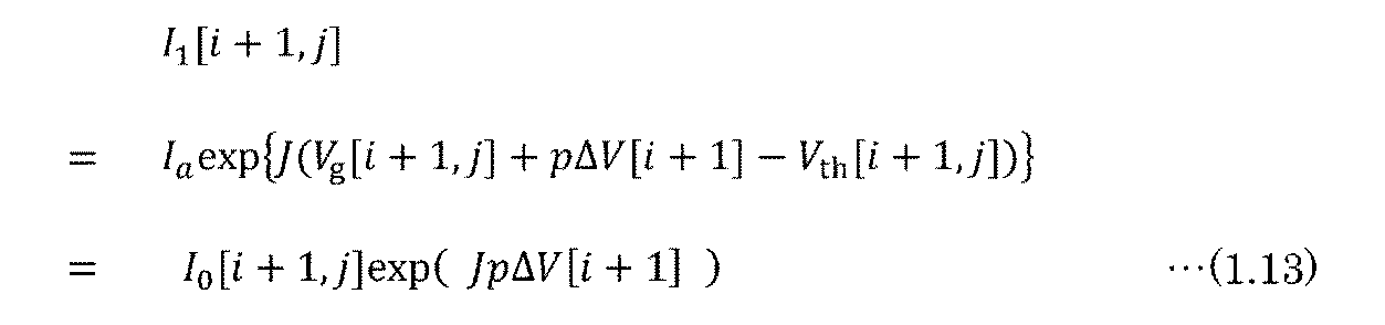

式(1.13)、及び式(1.14)より、x[i+1]は次の式で表すことができる。

そのため、式(1.13)は、次の式に書き換えることができる。

つまり、セルIM[i+1,j]に含まれているトランジスタF2の第1端子−第2端子間に流れる電流量は、第1データであるw[i+1,j]と、第2データであるx[i+1]と、の積に比例する。
ここで、変換回路ITRZ[j]から、トランジスタF4[j]と配線WCL[j]とを介して、セルIM[i,j]及びセルIM[i+1,j]に流れる電流量の総和を考える。当該電流量の総和をIS[j]とすると、IS[j]は、式(1.12)、及び式(1.16)より、次の式で表すことができる。

したがって、変換回路ITRZ[j]から出力される電流量は、第1データであるw[i,j]及びw[i+1,j]と、第2データであるx[i]及びx[i+1]と、の積和に比例した電流量となる。
なお、上述の動作例では、セルIM[i,j]、及びセルIM[i+1,j]に流れる電流量の総和について扱ったが、複数のセルとして、セルIM[1,j]乃至セルIM[m,j]のそれぞれに流れる電流量の総和についても扱ってもよい。この場合、式(1.17)は、次の式に書き直すことができる。

このため、3行以上且つ2列以上のセルアレイCAを有する演算回路MAC1の場合でも、上記の通り、積和演算を行うことができる。この場合の演算回路MAC1は、複数列のうち1列を、電流量としてIref0、及びxIref0を保持するセルとすることで、複数列のうち残りの列の数だけ積和演算処理を同時に実行することができる。つまり、メモリセルアレイの列の数を増やすことで、高速な積和演算処理を実現する半導体装置を提供することができる。
なお、上述した演算回路MAC1の動作例は、正の第1データと正の第2データとの積和を演算する場合に好適である。なお、正又は負の第1データと、正の第2データとの積和を演算する動作例、また、正又は負の第1データと、正又は負の第2データと、の積和を演算する動作例については、実施の形態3で説明する。
また、本実施の形態では、演算回路MAC1に含まれているトランジスタをOSトランジスタ、又はSiトランジスタとした場合について説明したが、本発明の一態様は、これに限定されない。演算回路MAC1に含まれているトランジスタは、例えば、Geなどがチャネル形成領域に含まれるトランジスタ、ZnSe、CdS、GaAs、InP、GaN、若しくはSiGeなどの化合物半導体がチャネル形成領域に含まれるトランジスタ、カーボンナノチューブがチャネル形成領域に含まれるトランジスタ、又は、有機半導体がチャネル形成領域に含まれるトランジスタ、などを用いることができる。
なお、本実施の形態は、本明細書等で示す他の実施の形態等と適宜組み合わせることができる。
(実施の形態3)
実施の形態2では、正、又は“0”の第1データと正、又は“0”の第2データとの積和を行う演算回路、及びその動作例について説明したが、本実施の形態では、正、負、又は“0”の第1データと、正、又は“0”の第2データと、の積和演算、及び、正、負、又は“0”の第1データと、正、負、又は“0”の第2データと、の積和演算が可能な演算回路について説明する。
実施の形態2では、正、又は“0”の第1データと正、又は“0”の第2データとの積和を行う演算回路、及びその動作例について説明したが、本実施の形態では、正、負、又は“0”の第1データと、正、又は“0”の第2データと、の積和演算、及び、正、負、又は“0”の第1データと、正、負、又は“0”の第2データと、の積和演算が可能な演算回路について説明する。
<演算回路の構成例1>
図13は、正、負、又は“0”の第1データと、正、又は“0”の第2データとの積和演算を行う演算回路の構成例を示している。図13に示す演算回路MAC2は、図5の演算回路MAC1を変更した構成となっている。そのため、演算回路MAC2の説明において、演算回路MAC1の説明と重複する部分については省略する。
図13は、正、負、又は“0”の第1データと、正、又は“0”の第2データとの積和演算を行う演算回路の構成例を示している。図13に示す演算回路MAC2は、図5の演算回路MAC1を変更した構成となっている。そのため、演算回路MAC2の説明において、演算回路MAC1の説明と重複する部分については省略する。
図13に示すセルアレイCAは、回路CES[1,j]乃至回路CES[m,j]を有し、回路CES[1,j]は、セルIM[1,j]と、セルIMr[1,j]と、を有し、回路CES[m,j]は、セルIM[m,j]と、セルIMr[m,j]と、を有する。なお、図13では、回路CES[1,j]と回路CES[m,j]とを抜粋して図示している。また、セルIM[1,j]が有するトランジスタF2のゲートをノードNN[1,j]と示し、セルIMr[1,j]が有するトランジスタF2rのゲートをノードNNr[1,j]と示し、セルIM[m,j]が有するトランジスタF2のゲートをノードNN[m,j]と示し、セルIMr[m,j]が有するトランジスタF2rのゲートをノードNNr[m,j]と示し、セルIMref[1]が有するトランジスタF2mのゲートをノードNNref[1]と示し、セルIMref[m]が有するトランジスタF2mのゲートをノードNNref[m]と示している。また、本明細書等では、例えば、回路CES[1,j]乃至回路CES[m,j]、セルIM[1,j]、セルIMr[1,j]、セルIM[m,j]、及びセルIMr[m,j]などを説明する際、それぞれの符号に付記している[m,n]などを省略する場合がある。
セルIMは、図5の演算回路MAC1のセルアレイCAに含まれているセルIM[1,1]乃至セルIM[m,n]と同様の構成とすることができる。
また、セルIMrは、セルIMと同様の構成とすることができる。図13のセルIMrは、一例として、セルIMと同様の構成として図示している。また、セルIMとセルIMrとのそれぞれに含まれている例えばトランジスタ及び容量などを互いに区別できるように、セルIMrに含まれているトランジスタ及び容量を示す符号には「r」を付している。
具体的には、セルIMrは、トランジスタF1rと、トランジスタF2rと、容量C5rと、を有する。なお、トランジスタF1rはセルIMのトランジスタF1に相当し、トランジスタF2rはセルIMのトランジスタF2に相当し、容量C5rはセルIMの容量C5に相当する。そのため、トランジスタF1rと、トランジスタF2rと、容量C5rと、のそれぞれの電気的な接続構成については、実施の形態2のIM[1,1]乃至セルIM[m,n]の説明を参酌する。
また、セルIMrにおいて、トランジスタF1rの第1端子と、トランジスタF2rのゲートと、容量C5rの第1端子と、の接続箇所をノードNNrとしている。
回路CES[1,j]において、容量C5の第2端子は、配線XCL[1]に電気的に接続され、トランジスタF1のゲートは、配線WSL[1]に電気的に接続され、トランジスタF1の第2端子とトランジスタF2の第2端子とは、配線WCL[j]に電気的に接続されている。また、容量C5rの第2端子は、配線XCL[1]に電気的に接続され、トランジスタF1rのゲートは、配線WSL[1]に電気的に接続され、トランジスタF1rの第2端子とトランジスタF2rの第2端子とは、配線WCLr[j]に電気的に接続されている。
同様に、回路CES[m,j]において、容量C5の第2端子は、配線XCL[m]に電気的に接続され、トランジスタF1のゲートは、配線WSL[m]に電気的に接続され、トランジスタF1の第2端子とトランジスタF2の第2端子とは、配線WCL[j]に電気的に接続されている。また、容量C5rの第2端子は、配線XCL[m]に電気的に接続され、トランジスタF1rのゲートは、配線WSL[m]に電気的に接続され、トランジスタF1rの第2端子とトランジスタF2rの第2端子とは、配線WCLr[j]に電気的に接続されている。
配線WCL[j]及び配線WCLr[j]のそれぞれは、実施の形態2で説明した配線WCL[1]乃至配線WCL[n]と同様に、一例として、回路WCSから回路CESに含まれているセルIMとセルIMrに電流を流す配線として機能する。また、一例として、変換回路ITRZD[j]から回路CESに含まれているセルIMとセルIMrに電流を流す配線として機能する。
また、図13の演算回路MAC2において、回路SWS1は、トランジスタF3[j]と、トランジスタF3r[j]と、を有する。トランジスタF3[j]の第1端子は、配線WCL[j]に電気的に接続され、トランジスタF3[j]の第2端子は、回路WCSに電気的に接続され、トランジスタF3[j]のゲートは、配線SWL1に電気的に接続されている。また、トランジスタF3r[j]の第1端子は、配線WCLr[j]に電気的に接続され、トランジスタF3r[j]の第2端子は、回路WCSに電気的に接続され、トランジスタF3r[j]のゲートは、配線SWL1に電気的に接続されている。
また、図13の演算回路MAC2において、回路SWS2は、トランジスタF4[j]と、トランジスタF4r[j]と、を有する。トランジスタF4[j]の第1端子は、配線WCL[j]に電気的に接続され、トランジスタF4[j]の第2端子は、変換回路ITRZD[j]に電気的に接続され、トランジスタF4[j]のゲートは、配線SWL2に電気的に接続されている。また、トランジスタF4r[j]の第1端子は、配線WCLr[j]に電気的に接続され、トランジスタF4r[j]の第2端子は、変換回路ITRZD[j]に電気的に接続され、トランジスタF4r[j]のゲートは、配線SWL2に電気的に接続されている。
変換回路ITRZD[j]は、演算回路MAC1における変換回路ITRZ[1]乃至変換回路ITRZ[n]に相当する回路であって、例えば、変換回路ITRZD[j]から配線WCL[j]に流れる電流の量と、変換回路ITRZD[j]から配線WCLr[j]に流れる電流の量と、の差分に応じた電圧を生成して、配線OL[j]に出力する機能を有する。
変換回路ITRZD[j]の具体的な構成例を図14Aに示す。図14Aに示す変換回路ITRZD1は、図13の変換回路ITRZD[j]に適用できる回路の一例である。なお、図14Aには、変換回路ITRZD1の周辺の回路との電気的な接続を示すため、回路SWS2、配線WCL、配線WCLr、配線SWL2、トランジスタF4、及びトランジスタF4rも図示している。また、配線WCL及び配線WCLrのそれぞれは、一例として、図13の演算回路MAC2に含まれている配線WCL[j]及び配線WCLr[j]とし、トランジスタF4及びトランジスタF4rは、一例として、図13の演算回路MAC2に含まれているトランジスタF4[j]及びトランジスタF4r[j]とすることができる。
図14Aの変換回路ITRZD1は、トランジスタF4を介して配線WCLに電気的に接続されている。また、変換回路ITRZD1は、トランジスタF4rを介して配線WCLrに電気的に接続されている。また、変換回路ITRZD1は、配線OLに電気的に接続されている。変換回路ITRZD1は、変換回路ITRZD1から配線WCLに流れる電流量、又は配線WCLから変換回路ITRZD1に流れる電流量を第1の電圧に変換する機能と、変換回路ITRZD1から配線WCLrに流れる電流量、又は配線WCLrから変換回路ITRZD1に流れる電流量を第2の電圧に変換する機能と、第1の電圧と第2の電圧との差に応じたアナログ電圧を配線OLに出力する機能と、を有する。
図14Aの変換回路ITRZD1は、一例として、抵抗RPと、抵抗RMと、オペアンプOPPと、オペアンプOPMと、オペアンプOP2と、を有する。
オペアンプOPPの反転入力端子は、抵抗RPの第1端子と、トランジスタF4の第2端子と、に電気的に接続されている。オペアンプOPPの非反転入力端子は、配線VRPLに電気的に接続されている。オペアンプOPPの出力端子は、抵抗RPの第2端子と、オペアンプOP2の非反転入力端子と、に電気的に接続されている。また、オペアンプOPMの反転入力端子は、抵抗RMの第1端子と、トランジスタF4rの第2端子と、に電気的に接続されている。オペアンプOPMの非反転入力端子は、配線VRMLに電気的に接続されている。オペアンプOPMの出力端子は、抵抗RMの第2端子と、オペアンプOP2の反転入力端子と、に電気的に接続されている。オペアンプOP2の出力端子は、配線OLに電気的に接続されている。
配線VRPLは、定電位を与える配線として機能する。当該定電位としては、例えば、接地電位(GND)、又は低レベル電位などとすることができる。また、配線VRMLは、定電位を与える配線として機能する。当該定電位としては、例えば、接地電位(GND)、又は低レベル電位などとすることができる。また、配線VRPL及び配線VRMLのそれぞれが与える定電位は、互いに等しくてもよいし、互いに異なっていてもよい。特に、配線VRPL及び配線VRMLのそれぞれが与える定電位を接地電位(GND)にすることによって、オペアンプOPPの反転入力端子、及びオペアンプOPMの反転入力端子のそれぞれを仮想接地にすることができる。
変換回路ITRZD1は、図14Aの構成にすることによって、配線WCLから、トランジスタF4を介して、変換回路ITRZD1に流れる電流量、又は、変換回路ITRZD1から、トランジスタF4を介して、配線WCLに流れる電流量を、第1の電圧に変換することができる。また、配線WCLrから、トランジスタF4rを介して、変換回路ITRZD1に流れる電流量、又は、変換回路ITRZD1から、トランジスタF4rを介して、配線WCLrに流れる電流量を、第2の電圧に変換することができる。そして、第1の電圧と第2の電圧との差に応じたアナログ電圧を配線OLに出力することができる。
また、図14Aの変換回路ITRZD1は、アナログ電圧を出力する構成となっているが、図13の変換回路ITRZD[j]に適用できる回路構成は、これに限定されない。例えば、変換回路ITRZD1は、図8Cと同様に、図14Bに示すとおり、アナログデジタル変換回路ADCを有する構成としてもよい。具体的には、図14Bの変換回路ITRZD2は、アナログデジタル変換回路ADCの入力端子がオペアンプOP2の出力端子に電気的に接続され、アナログデジタル変換回路ADCの出力端子が配線OLに電気的に接続されている構成となっている。このような構成にすることによって、図14Bの変換回路ITRZD2は、配線OLにデジタル信号を出力することができる。
また、変換回路ITRZD2において、配線OLに出力されるデジタル信号を1ビット(2値)とする場合、変換回路ITRZ2は、図14Cに示す変換回路ITRZD3に置き換えてもよい。図14Cの変換回路ITRZ3は、図8Cと同様に、図14Aの変換回路ITRZD1にコンパレータCMP2を設けた構成となっている。具体的には、変換回路ITRZD3は、コンパレータCMP2の第1入力端子がオペアンプOP2の出力端子に電気的に接続され、コンパレータCMP2の第2入力端子が配線VRL3に電気的に接続され、コンパレータCMP2の出力端子が配線OLに電気的に接続されている構成となっている。配線VRL3は、コンパレータCMP2の第1端子の電位と比較するための電位を与える配線として機能する。このような構成にすることによって、図14Cの変換回路ITRZD3は、トランジスタF4のソース−ドレイン間に流れる電流量から変換された第1の電圧とトランジスタF4rのソース−ドレイン間に流れる電流量から変換された第2の電圧との差と、配線VRL3が与える電圧と、との大小に応じて、配線OLに低レベル電位又は高レベル電位(2値のデジタル信号)を出力することができる。
<<第1データの保持の例>>
次に、図13の演算回路MAC2において、正、負、又は“0”の第1データと、正、又は“0”の第2データとの積和演算を行うための、第1データを回路CESに保持する一例について説明する。
次に、図13の演算回路MAC2において、正、負、又は“0”の第1データと、正、又は“0”の第2データとの積和演算を行うための、第1データを回路CESに保持する一例について説明する。
回路CESは、セルIMと、セルIMrと、を有するため、回路CESは、第1データの保持として、セルIMと、セルIMrと、の2つの回路を用いることができる。つまり、回路CESは、2つの電流量を設定して、それぞれの電流量に応じた電位をセルIMと、セルIMrと、に保持することができる。このため、第1データを、セルIMで設定される電流量と、セルIMrで設定される電流量と、で表すことができる。ここで、回路CESに保持される、正の第1データ、負の第1データ、又は“0”の第1データを次の通りに定義する。
回路CES[1,j]に正の第1データを保持する場合、セルIM[1,j]には、一例として、セルIM[1,j]のトランジスタF2の第1端子−第2端子間に正の第1データの値の絶対値に応じた電流量が流れるように設定する。具体的には、トランジスタF2のゲート(ノードNN[1,j])に当該電流量に応じた電位を保持する。一方、セルIMr[1,j]には、一例として、セルIMr[1,j]のトランジスタF2rの第1端子−第2端子間に電流が流れないように設定する。具体的には、トランジスタF2rのゲート(ノードNNr[1,j])には、例えば、配線VEが与える電位、又は、図6Aの回路WCSの配線VINIL1が与える初期化用の電位、などが保持されていればよい。
また、回路CES[1,j]に負の第1データを保持する場合、セルIMr[1,j]には、一例として、セルIMr[1,j]のトランジスタF2rには負の第1データの値の絶対値に応じた電流量が流れるように設定する。具体的には、トランジスタF2rのゲート(ノードNNr[1,j])に当該電流量に応じた電位を保持する。一方、セルIM[1,j]は、一例として、セルIM[1,j]のトランジスタF2には電流が流れないように設定する。具体的には、トランジスタF2のゲート(ノードNN[1,j])には、例えば、配線VEが与える電位、又は、図6Aの回路WCSの配線VINIL1が与える初期化用の電位、などが保持されていればよい。
また、回路CES[1,j]に“0”の第1データを保持する場合、一例として、セルIM[1,j]のトランジスタF2、及びセルIMr[1,j]のトランジスタF2rのそれぞれには電流が流れないように設定する。具体的には、トランジスタF2のゲート(ノードNN[1,j])及びトランジスタF2rのゲート(ノードNNr[1,j])には、例えば、配線VEが与える電位、又は、図6Aの回路WCSの配線VINIL1が与える初期化用の電位、などが保持されていればよい。
なお、他の回路CESについても、正の第1データ、又は負の第1データを保持するとき、上述した回路CES[1,j]と同様に、セルIMと配線WCLとの間、又は、セルIMrと配線WCLrとの間、の一方には第1データに応じた電流量が流れるように設定し、セルIMと配線WCLとの間、又は、セルIMrと配線WCLrとの間、の他方には電流が流れないように設定すればよい。また、他の回路CESに、“0”の第1データを保持するとき、上述した回路CES[1,j]と同様に、セルIMと配線WCLとの間、及びセルIMrと配線WCLrとの間には電流が流れないように設定すればよい。
例えば、“+3”、“+2”、“+1”、“0”、“−1”、“−2”、及び“−3”のそれぞれの場合を第1データとして回路CESに保持するとき、配線WCLからセルIMに流れる電流量の設定、及び配線WCLrからセルIMrに流れる電流量の設定を上記のとおりに従うことで、第1データ“+3”、“+2”、“+1”、“0”、“−1”、“−2”、及び“−3”のそれぞれは、次表のとおりに定義することができる。

ここで、図13の演算回路MAC2において、回路CES[1,j]乃至回路CES[m,j]のそれぞれに第1データが保持され、配線XCL[1]乃至配線XCL[m]のそれぞれに第2データが入力された場合を考える。このとき、配線SWL1に低レベル電位を与えてトランジスタF3[j]、及びトランジスタF3r[j]をオフ状態にし、このとき、配線SWL2に高レベル電位を与えてトランジスタF4[j]、及びトランジスタF4r[j]をオン状態にする。これにより、変換回路ITRZD[j]と配線WCL[j]との間が導通状態となるため、変換回路ITRZD[j]から配線WCL[j]に電流が流れる場合がある。また、変換回路ITRZD[j]と配線WCLr[j]との間が導通状態となるため、変換回路ITRZD[j]から配線WCLr[j]に電流が流れる場合がある。変換回路ITRZD[j]から配線WCL[j]に流れる電流量の総和をIS[j]とし、及び変換回路ITRZD[j]から配線WCLr[j]に流れる電流量の総和をISr[j]として、実施の形態2で説明した演算回路MAC1の動作例を参酌すると、IS[j]及びISr[j]は、次の式で表すことができる。

なお、式(2.1)に示すw[i,j]は、セルIM[i,j]に書き込まれる第1データの値であり、式(2.2)に示すwr[i,j]は、セルIMr[i,j]に書き込まれる第1データの値である。なお、w[i,j]、又はwr[i,j]の一方が“0”でない値であるとき、w[i,j]、又はwr[i,j]の他方は“0”の値とすることによって、回路CES[i,j]に保持される第1データは、例えば、表1に示した定義などに従うことができる。
変換回路ITRZD[j]は、例えば、配線WCLに流れる電流量の総和IS[j]を第1の電圧に変換し、配線WCLrに流れる電流量の総和ISr[j]を第2の電圧に変換する。そして、変換回路ITRZD[j]は、第1の電圧と第2の電圧との差に応じた電圧を配線OLに出力することができる。
ところで、図14A乃至図14Cのそれぞれに示した変換回路ITRZD1乃至変換回路ITRZD3は、配線OLに電圧を出力する回路構成としたが、本発明の一態様は、これに限定されない。例えば、図13の演算回路MAC2に含まれている変換回路ITRZD[j]は、電流を出力する回路構成としてもよい。
図15に示す変換回路ITRZD4は、図13の演算回路MAC2に含まれている変換回路ITRZD[j]に適用することができる回路であり、積和演算及び活性化関数の演算の結果を電流量として出力する回路構成となっている。
なお、図15には、変換回路ITRZD4の周辺の回路との電気的な接続を示すため、回路SWS2、配線WCL、配線WCLr、配線OL、トランジスタF4、及びトランジスタF4rも図示している。また、配線WCL及び配線WCLrのそれぞれは、一例として、図13の演算回路MAC2に含まれている配線WCL[j]及び配線WCLr[j]とし、トランジスタF4及びトランジスタF4rは、一例として、図13の演算回路MAC2に含まれているトランジスタF4[j]及びトランジスタF4r[j]とすることができる。
図15の変換回路ITRZD4は、トランジスタF4を介して配線WCLに電気的に接続されている。また、変換回路ITRZD4は、トランジスタF4rを介して配線WCLrに電気的に接続されている。また、変換回路ITRZD4は、配線OLに電気的に接続されている。変換回路ITRZD4は、変換回路ITRZD4から配線WCLに流れる電流量、又は配線WCLから変換回路ITRZD4に流れる電流量の一方と、変換回路ITRZD4から配線WCLrに流れる電流量、又は配線WCLrから変換回路ITRZD4に流れる電流量の一方と、の差分電流を取得する機能を有する。また、当該差分電流を、変換回路ITRZD4と配線OLとの間に流す機能を有する。
図15の変換回路ITRZD4は、一例として、トランジスタF5と、電流源CIと、電流源CIrと、カレントミラー回路CM1と、を有する。
トランジスタF4の第2端子は、カレントミラー回路CM1の第1端子と、電流源CIの出力端子と、に電気的に接続され、トランジスタF4rの第2端子は、カレントミラー回路CM1の第2端子と、電流源CIrの出力端子と、トランジスタF5の第1端子と、に電気的に接続されている。また、電流源CIの入力端子は、配線VHEに電気的に接続され、電流源CIrの入力端子は、配線VHEに電気的に接続されている。また、カレントミラー回路CM1の第3端子は、配線VSEに電気的に接続され、カレントミラー回路CM1の第4端子は、配線VSEに電気的に接続されている。
トランジスタF5の第2端子は、配線OLに電気的に接続され、トランジスタF5のゲートは、配線OELに電気的に接続されている。
カレントミラー回路CM1は、一例として、カレントミラー回路CM1の第1端子の電位に応じた電流量を、カレントミラー回路CM1の第1端子と第3端子との間と、カレントミラー回路CM1の第2端子と第4端子との間と、に流す機能を有する。
配線VHEは、例えば、定電位を与える配線として機能する。具体的には、当該定電位としては、例えば、高レベル電位などとすることができる。
配線VSEは、例えば、定電位を与える配線として機能する。具体的には、当該定電位としては、例えば、低レベル電位、又は接地電位などとすることができる。
配線OELは、例えば、トランジスタF5をオン状態、又はオフ状態に切り替えるための信号を送信するための配線として機能する。具体的には、例えば、配線OELには、高レベル電位、又は低レベル電位を入力すればよい。
電流源CIは、電流源CIの入力端子と出力端子との間に定電流を流す機能を有する。また、電流源CIrは、電流源CIrの入力端子と出力端子との間に定電流を流す機能を有する。なお、図15の変換回路ITRZD4において、電流源CIが流す電流の大きさと、電流源CIrが流す電流の大きさと、は等しいことが好ましい。
ここで、図15の変換回路ITRZD4の動作例について、説明する。
初めに、変換回路ITRZD4からトランジスタF4を介して配線WCLに流れる電流の量をISとし、変換回路ITRZD4からトランジスタF4rを介して配線WCLrに流れる電流の量をISrとする。また、電流源CI及び電流源CIrのそれぞれが流す電流の量をI0とする。
ISは、図13の演算回路MAC2において、例えば、j列目に位置するセルIM[1,j]乃至セルIM[m,j]に流れる電流量の総和とする。また、ISrは、図13の演算回路MAC2において、例えば、j列目に位置するセルIMr[1,j]乃至セルIMr[m,j]に流れる電流量の総和とする。
配線SWL2に高レベル電位が入力されることによって、トランジスタF4、及びトランジスタF4rはオン状態となる。このため、カレントミラー回路CM1の第1端子から第3端子に流れる電流量は、I0−ISとなる。また、カレントミラー回路CM1によって、カレントミラー回路CM1の第2端子から第4端子にI0−ISの電流量が流れる。
次に、配線OELに高レベル電位が入力されて、トランジスタF5がオン状態となる。このとき、配線OLに流れる電流量をIoutとすると、Iout=I0−(I0−IS)−ISr=IS−ISrとなる。
ここで、図13の演算回路MAC2において、正、負、又は“0”の第1データと、正、又は“0”の第2データとの積和演算を行うための、第1データの回路CESへの保持については、上記の第1データの保持の例を参酌する。
つまり、回路CES[i,j]に正の第1データを保持する場合、セルIM[i,j]には、セルIM[i,j]のトランジスタF2の第1端子−第2端子間に正の第1データの値の絶対値に応じた電流量が流れるように設定し、セルIMr[i,j]には、セルIMr[i,j]のトランジスタF2rの第1端子−第2端子間に電流が流れないように設定する。また、回路CES[i,j]に負の第1データを保持する場合、セルIM[i,j]には、セルIM[i,j]のトランジスタF2の第1端子−第2端子間に電流が流れないように設定し、セルIMr[i,j]には、セルIMr[i,j]のトランジスタF2rの第1端子−第2端子間に負の第1データの値の絶対値に応じた電流量が流れるように設定する。また、回路CES[i,j]に“0”の第1データを保持する場合、セルIM[i,j]には、セルIM[i,j]のトランジスタF2の第1端子−第2端子間に電流が流れないように設定し、セルIMr[i,j]には、セルIMr[i,j]のトランジスタF2rの第1端子−第2端子間に電流が流れないように設定する。
ここで、図13の演算回路MAC2の配線XCL[1]乃至配線XCL[m]のそれぞれに第2データが入力された場合、セルIM[i,j]のトランジスタF2の第1端子−第2端子間に流れる電流量、及びセルIMr[i,j]のトランジスタF2rの第1端子−第2端子間に流れる電流量のそれぞれは、第2データに比例する。
ISはj列目に位置するセルIM[1,j]乃至セルIM[m,j]に流れる電流量の総和である。そのため、ISは、回路CES[1,j]乃至回路CES[m,j]のうち、正の第1データが保持された回路CESに含まれている、セルIMに流れる電流量の総和となり、例えば、式(2.1)と同様に表すことができる。つまり、ISは、正の第1データの絶対値と第2データとの積和演算の結果に対応する。また、ISrはj列目に位置するセルIMr[1,j]乃至セルIMr[m,j]に流れる電流量の総和である。そのため、ISrは、回路CES[1,j]乃至回路CES[m,j]のうち、負の第1データが保持された回路CESに含まれている、セルIMrに流れる電流量の総和となり、例えば、式(2.2)と同様に表すことができる。つまり、ISrは、負の第1データの絶対値と第2データとの積和演算の結果に対応する。
このため、配線OLに流れる電流量Iout=IS−ISrは、正の第1データの絶対値と第2データとの積和演算の結果と、負の第1データの絶対値と第2データとの積和演算の結果と、の差に対応する。つまり、Iout=IS−ISrは、回路CES[1,j]乃至回路CES[m,j]に保持されている、負、“0”、又は正の第1データと、配線XCL[1]乃至配線XCL[m]のそれぞれに入力される第2データとの積和演算の結果に対応する。
ところで、セルIM[1,j]乃至セルIM[m,j]に流れる電流量の総和が、セルIMr[1,j]乃至セルIMr[m,j]に流れる電流量の総和よりも大きいとき、すなわちISがISrよりも大きいとき、Ioutは0よりも大きい電流量となり、変換回路ITRZD4から配線OLに流れる。一方、セルIM[1,j]乃至セルIM[m,j]に流れる電流量の総和が、セルIMr[1,j]乃至セルIMr[m,j]に流れる電流量の総和よりも小さいとき、すなわちISがISrよりも小さいとき、配線OLから変換回路ITRZD4に電流が流れない場合がある。つまり、ISがISrよりも小さいとき、Ioutは概ね0とすることができる。このため、変換回路ITRZD4は、例えば、ReLU関数として作用するとみなすことができる。
ReLU関数は、例えば、階層型のニューラルネットワークの活性化関数に利用することができる。階層型のニューラルネットワークの演算では、前層のニューロンのそれぞれの信号の値(例えば、第2データとすることができる)と、対応する重み係数(例えば、第1データとすることができる)と、の積和を算出する必要がある。また、積和の結果に応じて活性化関数の値を計算する必要がある。このため、階層型のニューラルネットワークの活性化関数をReLU関数とした場合、当該ニューラルネットワークの演算は、変換回路ITRZD4を含む演算回路MAC2を用いることによって行うことができる。
なお、階層型のニューラルネットワークについては、実施の形態4で後述する。
次に、図15の変換回路ITRZD4の具体的な回路構成の例について説明する。
図16Aに示す変換回路ITRZD4は、図15の変換回路ITRZD4の一例である。具体的には、図16Aでは、カレントミラー回路CM1、電流源CI、及び電流源CIrのそれぞれの構成の例を示している。
図16Aの変換回路ITRZD4において、カレントミラー回路CM1は、一例として、トランジスタF6と、トランジスタF6rと、を有し、電流源CIは、一例として、トランジスタF7を有し、電流源CIrは、一例として、トランジスタF7rを有する。なお、トランジスタF6、トランジスタF6r、トランジスタF7、及びトランジスタF7rは、nチャネル型トランジスタとしている。
例えば、カレントミラー回路CM1の第1端子は、トランジスタF6の第1端子と、トランジスタF6のゲートと、トランジスタF6rのゲートと、に電気的に接続され、カレントミラー回路CM1の第3端子は、トランジスタF6の第2端子に電気的に接続されている。また、カレントミラー回路CM1の第2端子は、トランジスタF6rの第1端子に電気的に接続され、カレントミラー回路CM1の第4端子は、トランジスタF6rの第2端子に電気的に接続されている。
また、例えば、電流源CIの出力端子は、トランジスタF7の第1端子と、トランジスタF7のゲートと、に電気的に接続され、電流源CIの入力端子は、トランジスタF7の第2端子に電気的に接続されている。
また、例えば、電流源CIrの出力端子は、トランジスタF7rの第1端子と、トランジスタF7rのゲートと、に電気的に接続され、電流源CIrの入力端子は、トランジスタF7rの第2端子に電気的に接続されている。
トランジスタF7、及びトランジスタF7rのそれぞれは、ゲートと第1端子とが電気的に接続されており、かつ第2端子と配線VHEとが電気的に接続されている。したがって、トランジスタF7、及びトランジスタF7rのそれぞれのゲート−ソース間電圧は0Vとなり、トランジスタF7、及びトランジスタF7rのそれぞれのしきい値電圧が適切な範囲内である場合、トランジスタF7、及びトランジスタF7rのそれぞれの第1端子−第2端子間には、サブスレッショルド領域で動作するときの電流範囲の電流が流れる。つまり、トランジスタF7、及びトランジスタF7rのそれぞれは定電流源として機能する。
なお、図15の変換回路ITRZD4に含まれる電流源CI、及び電流源CIrの構成は、図16Aに示した電流源CI、及び電流源CIrに限定されない。変換回路ITRZD4に含まれる電流源CI、及び電流源CIrのそれぞれの構成は、状況に応じて、変更を行ってもよい。
例えば、図15の変換回路ITRZD4に含まれる電流源CI、及び電流源CIrのそれぞれは、図16Bに示す構成としてもよい。
図16Bの電流源CI(電流源CIr)は、一例として、複数の電流源CSAを有する。また、複数の電流源CSAのそれぞれは、トランジスタF7と、トランジスタF7sと、端子U1と、端子U2と、端子U3と、を有する。
電流源CSAは、一例として、端子U2と端子U1との間に電流量としてICSAを流す機能を有する。また、電流源CI(電流源CIr)は、例えば、2P−1個(Pは1以上の整数である)の電流源CSAを有するものとしたとき、電流源CI(電流源CIr)は、出力端子に電流量としてs×ICSA(sは0以上2P−1以下の整数である)を流すことができる。
なお、実際には、電流源CI(電流源CIr)の作製段階において、それぞれの電流源CSAに含まれているトランジスタの電気特性のバラツキによって誤差が現れることがある。そのため、複数の電流源CSAの端子U1のそれぞれから出力される定電流ICSAの誤差は10%以内が好ましく、5%以内であることがより好ましく、1%以内であることがより好ましい。なお、本実施の形態では、電流源CI(電流源CIr)に含まれている複数の電流源CSAの端子U1から出力される定電流ICSAの誤差は無いものとして説明する。
複数の電流源CSAの一において、トランジスタF7sの第1端子は、端子U1に電気的に接続され、トランジスタF7sのゲートは、端子U3に電気的に接続されている。トランジスタF7の第1端子は、トランジスタF7のゲートと、トランジスタF7sの第2端子と、に電気的に接続されている。トランジスタF7の第2端子は、端子U2に電気的に接続されている。
複数の電流源CSAのそれぞれの端子U1は、電流源CI(電流源CIr)の出力端子に電気的に接続されている。また、複数の電流源CSAのそれぞれの端子U2は、電流源CI(電流源CIr)の入力端子に電気的に接続されている。つまり、複数の電流源CSAのそれぞれの端子U2と、配線VHEと、の間は導通となっている。
また、1個の電流源CSAの端子U3は配線CL[1]に電気的に接続され、2個の電流源CSAの端子U3のそれぞれは配線CL[2]に電気的に接続され、2P−1個の電流源CSの端子U3のそれぞれは配線CL[P]に電気的に接続されている。
配線CL[1]乃至配線CL[P]は、電気的に接続されている電流源CSAから定電流ICSAを出力するための制御信号を送信する配線として機能する。具体的には、例えば、配線CL[1]に高レベル電位が与えられているとき、配線CL[1]に電気的に接続されている電流源CSAは、定電流としてICSAを端子U1に流し、また、配線CL[1]に低レベル電位が与えられているとき、配線CL[1]に電気的に接続されている電流源CSAは、ICSAを出力しない。また、例えば、配線CL[2]に高レベル電位が与えられているとき、配線CL[2]に電気的に接続されている2個の電流源CSAは、合計2ICSAを定電流として端子U1に流し、また、配線CL[2]に低レベル電位が与えられているとき、配線CL[2]に電気的に接続されている電流源CSAは、合計2ICSAの定電流を出力しない。また、例えば、配線CL[P]に高レベル電位が与えられているとき、配線CL[P]に電気的に接続されている2P−1個の電流源CSAは、合計2P−1ICSAを定電流として端子U1に流し、また、配線CL[P]に低レベル電位が与えられているとき、配線CL[P]に電気的に接続されている電流源CSAは、合計2P−1ICSAの定電流を出力しない。
このため、電流源CI(電流源CIr)は、配線CL[1]乃至配線CL[P]から選ばれた一本以上の配線に高レベル電位を与えることによって、電流源CI(電流源CIr)の出力端子に電流を流すことができる。また、当該電流の量は、高レベル電位を入力する、配線CL[1]乃至配線CL[P]から選ばれた一本以上の配線の組み合わせによって定めることができる。例えば、配線CL[1]及び配線CL[2]に高レベル電位が与えられ、配線CL[3](図示せず)乃至配線CL[P]に低レベル電位が与えられているとき、電流源CI(電流源CIr)は、電流源CI(電流源CIr)の出力端子に合計3ICSAの電流を流すことができる。
上記の通り、図16Bの電流源CI(電流源CIr)を用いることによって、状況に応じて、電流源CI(電流源CIr)が出力端子に流す電流量を変化させることができる。
また、図15の変換回路ITRZD4として、図16Aの変換回路ITRZD4を適用することによって、変換回路ITRZD4に含まれるすべてのトランジスタをOSトランジスタとすることができる。また、例えば、演算回路MAC2のセルアレイCA、回路WCS、及び回路XCSなどは、OSトランジスタのみで構成することができるため、変換回路ITRZD4は、セルアレイCA、回路WCS、及び回路XCSなどと同時に作製することができる。そのため、演算回路MAC2の作製工程を短縮することができる場合がある。なお、これは、図16Aの変換回路ITRZD4の電流源CI及び電流源CIrに図16Bの電流源CI(電流源CIr)を適用した場合についても同様である。
例えば、図15の変換回路ITRZD4に含まれる電流源CI、及び電流源CIrのそれぞれは、互いに同じ電流を流す必要があるため、電流源CI、及び電流源CIrのそれぞれをカレントミラー回路に置き換えてもよい。
図17Aに示す変換回路ITRZD4は、図15の変換回路ITRZD4に含まれる電流源CI、及び電流源CIrのそれぞれをカレントミラー回路CM2に置き換えた構成となっている。カレントミラー回路CM2は、一例として、トランジスタF8と、トランジスタF8rと、を有する。なお、トランジスタF8、及びトランジスタF8rは、pチャネル型トランジスタとしている。
トランジスタF8の第1端子は、トランジスタF8のゲートと、トランジスタF8rのゲートと、トランジスタF4の第2端子と、カレントミラー回路CM1の第1端子と、に電気的に接続されている。トランジスタF8の第2端子は、配線VHEに電気的に接続されている。トランジスタF8rの第1端子は、トランジスタF4rの第2端子と、カレントミラー回路CM1の第2端子と、に電気的に接続されている。トランジスタF8rの第2端子は、配線VHEに電気的に接続されている。
図17Aの変換回路ITRZD4のとおり、図15の変換回路ITRZD4に含まれる電流源CI、及び電流源CIrのそれぞれをカレントミラー回路CM2に置き換えることによって、トランジスタF4の第2端子とカレントミラー回路CM1の第1端子との接続点、及びトランジスタF4rの第2端子とカレントミラー回路CM1の第2端子とトランジスタF5の第1端子との接続点のそれぞれに互いにほぼ等しい電流量を流すことができる。
なお、図17Aでは、カレントミラー回路CM2をトランジスタF8と、トランジスタF8rと、からなる構成として図示したが、カレントミラー回路CM2の回路構成は、これに限定されない。例えば、カレントミラー回路CM2は、後述する図17Cと同様に、カレントミラー回路CM2に含まれるトランジスタをカスコード接続した構成としてもよい。このように、図17Aのカレントミラー回路CM2の回路構成は、状況に応じて変更を行ってもよい。
なお、図17Aの変換回路ITRZD4は、図17Bに示す変換回路ITRZD4に構成のとおり、カレントミラー回路CM1を設けない構成としてもよい。図17Bに示す変換回路ITRZD4は、カレントミラー回路CM2の第1端子からトランジスタF4の第2端子に流れる電流量と、カレントミラー回路CM2の第2端子からトランジスタF4rの第2端子とトランジスタF5の第1端子との接続点に流れる電流量と、を互いにほぼ等しくすることができる。そのため、ISがISrよりも大きい場合に、図17Bの配線OLに流れる電流量は、図15の変換回路ITRZD4と同様にIS−ISrとすることができる。
図17Bの変換回路ITRZD4は、カレントミラー回路CM1を設けない構成となっているため、図17Aの変換回路ITRZD4よりも回路面積を低減することができる。また、カレントミラー回路CM2からカレントミラー回路CM1に流れる定常電流が無くなるため、図17Bの変換回路ITRZD4は、図17Aの変換回路ITRZD4よりも消費電力を低減することができる。
なお、図17Bでは、トランジスタF8、及びトランジスタF8rを図示せず、カレントミラー回路CM2をブロック図として図示している。そのため、図17Bのカレントミラー回路CM2は、図17Aのカレントミラー回路CM2と同様に、状況に応じて、構成を決めることができる。
また、図15の変換回路ITRZD4に含まれるカレントミラー回路CM1は、図16Aに示したカレントミラー回路CM1に限定されない。図16Aの変換回路ITRZD4に含まれるカレントミラー回路CM1の構成は、状況に応じて、変更を行ってもよい。
例えば、図15の変換回路ITRZD4に含まれるカレントミラー回路CM1は、図17Cに示すカレントミラー回路CM1としてもよい。図17Cに示すカレントミラー回路CM1は、図16Aに示すカレントミラー回路CM1に更にnチャネル型トランジスタであるトランジスタF6s及びトランジスタF6srを設けて、トランジスタF6とトランジスタF6sとでカスコード接続し、トランジスタF6rとトランジスタF6srとでカスコード接続した構成となっている。図17Cのとおり、カレントミラー回路に含まれるトランジスタをカスコード接続することによって、当該カレントミラー回路の動作をより安定させることができる。
<演算回路の構成例2>
図18は、正、負、又は“0”の第1データと、正、負、又は“0”の第2データと、の積和演算を行う演算回路の構成例を示している。図18に示す演算回路MAC3は、図13の演算回路MAC2を変更した構成となっている。そのため、演算回路MAC3の説明において、演算回路MAC1及び演算回路MAC2の説明と重複する部分については省略する。
図18は、正、負、又は“0”の第1データと、正、負、又は“0”の第2データと、の積和演算を行う演算回路の構成例を示している。図18に示す演算回路MAC3は、図13の演算回路MAC2を変更した構成となっている。そのため、演算回路MAC3の説明において、演算回路MAC1及び演算回路MAC2の説明と重複する部分については省略する。
図18に示す回路CES[i,j]は、セルIM[i,j]と、セルIMr[i,j]と、に加え、セルIMs[i,j]と、セルIMsr[i,j]と、を有する。なお、図18では、回路CES[i,j]を図示しており、それ以外の回路CESについては省略する。また、本明細書等では、例えば、回路CES[i,j]、セルIM[i,j]、セルIMr[i,j]、セルIMs[i,j]、及びセルIMsr[i,j]などを説明する際、それぞれの符号に付記している[i,j]などを省略する場合がある。
セルIMs及びセルIMsrは、セルIMと同様の構成とすることができる。図18のセルIMs及びセルIMsrは、一例として、セルIMと同様の構成として図示している。また、セルIMとセルIMsとセルIMsrとのそれぞれに含まれている例えばトランジスタ及び容量などを互いに区別できるように、セルIMsに含まれているトランジスタ及び容量を示す符号には「s」を付し、セルIMsrに含まれているトランジスタ及び容量を示す符号には「sr」を付している。
具体的には、セルIMsは、トランジスタF1sと、トランジスタF2sと、容量C5sと、を有する。なお、トランジスタF1sはセルIMのトランジスタF1に相当し、トランジスタF2sはセルIMのトランジスタF2に相当し、容量C5sはセルIMの容量C5に相当する。そのため、トランジスタF1sと、トランジスタF2sと、容量C5sと、のそれぞれの電気的な接続構成については、実施の形態2のIM[1,1]乃至セルIM[m,n]の説明を参酌する。
また、セルIMsrは、トランジスタF1srと、トランジスタF2srと、容量C5srと、を有する。なお、トランジスタF1srはセルIMのトランジスタF1に相当し、トランジスタF2srはセルIMのトランジスタF2に相当し、容量C5srはセルIMの容量C5に相当する。そのため、トランジスタF1srと、トランジスタF2srと、容量C5srと、のそれぞれの電気的な接続構成については、セルIMrと同様に、実施の形態2のIM[1,1]乃至セルIM[m,n]の説明を参酌する。
また、セルIMsにおいて、トランジスタF1sの第1端子と、トランジスタF2sのゲートと、容量C5sの第1端子と、の接続箇所をノードNNsとし、セルIMsrにおいて、トランジスタF1srの第1端子と、トランジスタF2srのゲートと、容量C5srの第1端子と、の接続箇所をノードNNsrとしている。
回路CES[i,j]において、容量C5の第2端子は、配線XCL[i]に電気的に接続され、トランジスタF1のゲートは、配線WSL[i]に電気的に接続され、トランジスタF1の第2端子とトランジスタF2の第2端子とは、配線WCL[j]に電気的に接続されている。また、容量C5rの第2端子は、配線XCL[i]に電気的に接続され、トランジスタF1rのゲートは、配線WSL[i]に電気的に接続され、トランジスタF1rの第2端子とトランジスタF2rの第2端子とは、配線WCLr[j]に電気的に接続されている。
また、容量C5sの第2端子は、配線XCLs[i]に電気的に接続され、トランジスタF1sのゲートは、配線WSLs[i]に電気的に接続され、トランジスタF1sの第2端子とトランジスタF2sの第2端子とは、配線WCL[j]に電気的に接続されている。また、容量C5srの第2端子は、配線XCLs[i]に電気的に接続され、トランジスタF1srのゲートは、配線WSLs[i]に電気的に接続され、トランジスタF1srの第2端子とトランジスタF2srの第2端子とは、配線WCLr[j]に電気的に接続されている。
図18に示す回路CESref[i]は、セルIMref[i]に加え、セルIMrefs[i]を有する。なお、図18では、回路CESref[i]を図示しており、それ以外の回路CESrefについては省略する。また、本明細書等では、例えば、回路CESref[i]、セルIMref[i]、及びセルIMrefs[i]などを説明する際、それぞれの符号に付記している[i]などを省略する場合がある。
セルIMrefsは、セルIMrefと同様の構成とすることができる。図18のセルIMrefsは、一例として、セルIMrefと同様の構成として図示している。また、セルIMrefとセルIMrefsとのそれぞれに含まれている例えばトランジスタ及び容量などを互いに区別できるように、セルIMrefsに含まれているトランジスタ及び容量を示す符号には「s」を付している。
具体的には、セルIMrefsは、トランジスタF1msと、トランジスタF2msと、容量C5msと、を有する。なお、トランジスタF1msはセルIMrefのトランジスタF1mに相当し、トランジスタF2msはセルIMrefのトランジスタF2mに相当し、容量C5msはセルIMrefの容量C5mに相当する。そのため、トランジスタF1msと、トランジスタF2msと、容量C5msと、のそれぞれの電気的な接続構成については、実施の形態2のIMref[1]乃至セルIMref[m]の説明を参酌する。
また、セルIMrefsにおいて、トランジスタF1msの第1端子と、トランジスタF2msのゲートと、容量C5msの第1端子と、の接続箇所をノードNNrefsとしている。
回路CESref[i]において、容量C5mの第2端子は、配線XCL[i]に電気的に接続され、トランジスタF1mのゲートは、配線WSL[i]に電気的に接続され、トランジスタF1mの第2端子とトランジスタF2mの第2端子とは、配線XCL[i]に電気的に接続されている。また、容量C5msの第2端子は、配線XCLs[i]に電気的に接続され、トランジスタF1msのゲートは、配線WSLs[i]に電気的に接続され、トランジスタF1msの第2端子とトランジスタF2msの第2端子とは、配線XCLs[i]に電気的に接続されている。
配線XCL[i]及び配線XCLs[i]のそれぞれは、実施の形態2で説明した配線XCL[1]乃至配線XCL[m]と同様に、一例として、回路XCSから回路CESに含まれているセルIMとセルIMrとセルIMsとセルIMsrとに電流を流す配線、また、一例として、回路XCSから回路CESrefに含まれているセルIMrefとセルIMrefsとに電流を流す配線、として機能する。
配線WSL[i]及び配線WSLs[i]のそれぞれは、実施の形態2で説明した配線WSL[1]乃至配線WSL[m]と同様に、一例として、回路WSDから回路CESに含まれているセルIMとセルIMrとセルIMsとセルIMsrとに対して、第1データを書き込むための選択信号を送信する配線、また、一例として、回路WSDから回路CESrefに含まれているセルIMrefとセルIMrefsとに対して、参照データを書き込むための選択信号を送信する配線として機能する。
図18の演算回路MAC3に含まれる変換回路ITRZD[j]としては、図13の演算回路MAC2に含まれる変換回路ITRZD[j]に適用できる回路を用いることができる。つまり、演算回路MAC3に含まれる変換回路ITRZD[j]としては、例えば、図14A乃至図14Cに示す変換回路ITRZD1乃至変換回路ITRZD3を適用することができる。
<<第1データの保持及び第2データの入力の例>>
次に、図18の演算回路MAC3において、正、負、又は“0”の第1データと、正、負、又は“0”の第2データとの積和演算を行うための、第1データを回路CESに保持する一例、及び第2データを回路CESに入力する一例について説明する。
次に、図18の演算回路MAC3において、正、負、又は“0”の第1データと、正、負、又は“0”の第2データとの積和演算を行うための、第1データを回路CESに保持する一例、及び第2データを回路CESに入力する一例について説明する。
回路CESは、セルIMと、セルIMrと、セルIMsと、セルIMsrと、を有するため、回路CESは、第1データの保持として、セルIMと、セルIMrと、セルIMsと、セルIMsrと、の4つの回路を用いることができる。つまり、回路CESは、4つの電流量を設定して、それぞれの電流量に応じた電位をセルIMと、セルIMrと、セルIMsと、セルIMsrと、に保持することができる。このため、第1データを、セルIMで設定される電流量と、セルIMrで設定される電流量と、セルIMsで設定される電流量と、セルIMsrで設定される電流量と、で表すことができる。ここで、回路CESに保持される、正の第1データ、負の第1データ、又は“0”の第1データを次の通りに定義する。
回路CES[i,j]に正の第1データを保持する場合、セルIM[i,j]には、一例として、セルIM[i,j]のトランジスタF2には正の第1データの値の絶対値に応じた電流量が流れるように設定し、また、セルIMsr[i,j]のトランジスタF2srには、一例として、正の第1データの値の絶対値に応じた電流量が流れるように設定する。具体的には、トランジスタF2のゲート(ノードNN[i,j])及びトランジスタF2srのゲート(ノードNNsr[i,j])に当該電流量に応じた電位を保持する。また、セルIMr[i,j]には、一例として、セルIMr[i,j]のトランジスタF2rには電流が流れないように設定し、また、セルIMs[i,j]には、一例として、セルIMs[i,j]のトランジスタF2sには電流が流れないように設定する。具体的には、トランジスタF2rのゲート(ノードNNr[i,j])及びトランジスタF2sのゲート(ノードNNs[i,j])には、例えば、配線VEが与える電位、又は、図6Aの回路WCSの配線VINIL1が与える初期化用の電位、などが保持されればよい。
また、回路CES[i,j]に負の第1データを保持する場合、セルIMr[i,j]には、一例として、セルIMr[1,j]のトランジスタF2rには負の第1データの値の絶対値に応じた電流量が流れるように設定し、また、セルIMs[i,j]のトランジスタF2sには、一例として、負の第1データの値の絶対値に応じた電流量が流れるように設定する。具体的には、トランジスタF2rのゲート(ノードNNr[i,j])及びトランジスタF2sのゲート(ノードNNs[i,j])に当該電流量に応じた電位を保持する。また、セルIM[i,j]には、一例として、セルIM[i,j]のトランジスタF2には電流が流れないように設定し、また、セルIMsr[i,j]には、一例として、セルIMsr[i,j]のトランジスタF2srには電流が流れないように設定する。具体的には、トランジスタF2のゲート(ノードNN[i,j])及びトランジスタF2srのゲート(ノードNNsr[i,j])には、例えば、配線VEが与える電位、又は、図6Aの回路WCSの配線VINIL1が与える初期化用の電位、などが保持されればよい。
また、回路CES[i,j]に“0”の第1データを保持する場合、一例として、セルIM[i,j]のトランジスタF2、セルIMr[i,j]のトランジスタF2r、セルIMs[i,j]のトランジスタF2s、及びセルIMsr[i,j]のトランジスタF2srのそれぞれには電流が流れないように設定する。具体的には、トランジスタF2のゲート(ノードNN[i,j])とトランジスタF2rのゲート(ノードNNr[i,j])とトランジスタF2sのゲート(ノードNNs[i,j])及びトランジスタF2srのゲート(ノードNNsr[i,j])には、例えば、配線VEが与える電位、又は、図6Aの回路WCSの配線VINIL1が与える初期化用の電位、などが保持されればよい。
なお、他の回路CESについても、正の第1データ、又は負の第1データを保持するとき、上述した回路CES[i,j]と同様に、セルIMと配線WCLとの間及びセルIMsrと配線WCLrとの間、又は、セルIMrと配線WCLrとの間及びセルIMsと配線WCLとの間、の一方には第1データに応じた電流量が流れるように設定し、その他方には電流が流れないように設定すればよい。また、他の回路CESに、“0”の第1データを保持するとき、上述した回路CES[i,j]と同様に、セルIMと配線WCLとの間、セルIMrと配線WCLrとの間、セルIMsと配線WCLとの間、及びセルIMsrと配線WCLsrとの間、には電流が流れないように設定すればよい。
例えば、第1データとして“+3”、“+2”、“+1”、“0”、“−1”、“−2”、及び“−3”のそれぞれの場合において回路CESに保持する場合、配線WCLからセルIMに流れる電流量の設定、配線WCLrからセルIMrに流れる電流量の設定、配線WCLからセルIMsに流れる電流量の設定、及び配線WCLsrからセルIMsrに流れる電流量の設定を上記のとおりに従うことで、第1データ“+3”、“+2”、“+1”、“0”、“−1”、“−2”、及び“−3”のそれぞれは、次表のとおりに定義することができる。

一方、回路CESには、第2データを入力する配線として、配線XCLと配線XCLsとが電気的に接続されている。このため、回路CESには、第2データとして、2つの信号を入力することができる。つまり、第2データを、配線XCLに入力される信号と、配線XCLsに入力される信号と、で表して、回路CESに入力することができる。ここで、回路CESに入力される、正の第2データ、負の第2データ、又は“0”の第2データを次の通りに定義する。
回路CES[i,j]に正の第2データを入力する場合、セルIMref[i]には、一例として、セルIMref[i]のトランジスタF2mには正の第2データの値の絶対値に応じた電流量が流れるように設定する。具体的には、トランジスタF2mのゲート(ノードNNref[i])に当該電流量に応じた電位を保持する。一方、セルIMrefs[i]には、一例として、セルIMrefs[i]のトランジスタF2msには電流が流れないように設定する。具体的には、トランジスタF2msのゲート(ノードNNrefs[i])には、例えば、配線VEが与える電位、又は、図6Cの回路XCSの配線VINIL2が与える初期化用の電位、などが保持されればよい。
また、回路CES[i,j]に負の第2データを入力する場合、セルIMrefs[i]には、一例として、セルIMrefs[i]のトランジスタF2msには負の第2データの値の絶対値に応じた電流量が流れるように設定する。具体的には、トランジスタF2msのゲート(ノードNNrefs[i])に当該電流量に応じた電位を保持する。一方、セルIMref[i]には、一例として、セルIMref[i]のトランジスタF2mには電流が流れないように設定する。具体的には、トランジスタF2mのゲート(ノードNNref[i])には、例えば、配線VEが与える電位、又は、図6Cの回路XCSの配線VINIL2が与える初期化用の電位、などが保持されればよい。
また、回路CES[i,j]に“0”の第2データを入力する場合、一例として、セルIMref[i]のトランジスタF2m、及びセルIMrefs[1]のトランジスタF2msのそれぞれには電流が流れないように設定する。具体的には、トランジスタF2mのゲート(ノードNNref[i])及びトランジスタF2msのゲート(ノードNNrefs[i])には、例えば、配線VEが与える電位、又は、図6Cの回路XCSの配線VINIL2が与える初期化用の電位、などが保持されればよい。
なお、他の回路CESに対して、正の第2データ、又は負の第2データを入力するとき、上述した回路CESref[i]と同様に、セルIMrefと配線XCLとの間、又は、セルIMrefsと配線XCLsとの間、の一方には第2データに応じた電流量が流れるように設定し、セルIMrefと配線XCLとの間、又は、セルIMrefsと配線XCLsとの間、の他方には電流が流れないように設定すればよい。また、他の回路CESに、“0”の第2データを入力するとき、上述した回路CESref[i]と同様に、セルIMrefと配線XCLとの間、及びセルIMrefsと配線XCLsとの間には電流が流れないように設定すればよい。
一例えば、第2データとして“+3”、“+2”、“+1”、“0”、“−1”、“−2”、及び“−3”のそれぞれの場合において回路CESに入力される場合、配線XCLからセルIMrefに流れる電流量の設定、及び配線XCLsからセルIMrefsに流れる電流量の設定を上記のとおりに従うことで、第2データ“+3”、“+2”、“+1”、“0”、“−1”、“−2”、及び“−3”のそれぞれは、次表のとおりに定義することができる。

ここで、回路CESに保持される第1データとして“+3”、“+2”、“+1”、“0”、“−1”、“−2”、及び“−3”のいずれか一とし、かつ回路CESに入力される第2データとして“+1”、“0”、及び“−1”のいずれか一としたときにおいて、配線WCLから回路CESのセルIM及びセルIMsに流れる電流量、及び配線WCLrから回路CESのセルIMr及びセルIMsrに流れる電流量について考える。
例えば、回路CESに入力される第2データを“+1”としたとき、回路CESの容量C5及び容量C5rのそれぞれの第2端子には、配線XCLから第2データである“+1”の絶対値に応じた電位が入力され、回路CESの容量C5s及び容量C5srのそれぞれの第2端子には、配線XCLsから接地電位(GND)に応じた電位が入力されるものとする。また、回路CESに保持されている第1データを“+3”としたとき、ノードNN及びノードNNsrのそれぞれには第1データである“+3”の絶対値に応じた電位が保持され、ノードNNr及びノードNNsのそれぞれには接地電位(GND)が保持されているものとする。このとき、回路CESのトランジスタF2の第1端子−第2端子間には、式(1.12)又は式(1.16)より3Iref0の電流量が流れる。また、トランジスタF2r、トランジスタF2s、及びトランジスタF2srのそれぞれの第1端子−第2端子間には、電流は流れない。つまり、配線WCLからセルIMに3Iref0の電流量が流れ、配線WCLからセルIMsに電流が流れず、配線WCLrからセルIMrに電流が流れず、配線WCLrからセルIMsrに電流が流れない。
また、例えば、回路CESに入力される第2データを“+1”とし、回路CESに保持されている第1データを“−3”とする。このため、ノードNNr及びノードNNsのそれぞれには第1データである“−3”の絶対値に応じた電位が保持され、ノードNN及びノードNNsrのそれぞれには接地電位(GND)が保持されているものとする。このとき、回路CESのトランジスタF2rの第1端子−第2端子間には、式(1.12)又は式(1.16)より3Iref0の電流量が流れる。また、トランジスタF2、トランジスタF2s、及びトランジスタF2srのそれぞれの第1端子−第2端子間には、電流は流れない。つまり、配線WCLrからセルIMrに3Iref0の電流量が流れ、配線WCLからセルIMに電流が流れず、配線WCLからセルIMsに電流が流れず、配線WCLrからセルIMsrに電流が流れない。
また、例えば、回路CESに入力される第2データを“−1”としたとき、回路CESの容量C5s及び容量C5srのそれぞれの第2端子には、配線XCLsから第2データである“−1”の絶対値に応じた電位が入力され、回路CESの容量C5及び容量C5rのそれぞれの第2端子には、配線XCLから接地電位(GND)に応じた電位が入力されるものとする。また、回路CESに保持されている第1データを“+3”としたとき、ノードNN及びノードNNsrのそれぞれには第1データである“+3”の絶対値に応じた電位が保持され、ノードNNr及びノードNNsのそれぞれには接地電位(GND)が保持されているものとする。このとき、回路CESのトランジスタF2srの第1端子−第2端子間には、式(1.12)又は式(1.16)より3Iref0の電流量が流れる。また、トランジスタF2、トランジスタF2r、及びトランジスタF2sのそれぞれの第1端子−第2端子間には、電流は流れない。つまり、配線WCLrからセルIMsrに3Iref0の電流量が流れ、配線WCLからセルIMに電流が流れず、配線WCLrからセルIMrに電流が流れず、配線WCLからセルIMsに電流が流れない。
また、例えば、回路CESに入力される第2データを“−1”とし、回路CESに保持されている第1データを“−3”とする。このため、ノードNNr及びノードNNsのそれぞれには第1データである“−3”の絶対値に応じた電位が保持され、ノードNN及びノードNNsrのそれぞれには接地電位(GND)が保持されているものとする。このとき、回路CESのトランジスタF2sの第1端子−第2端子間には、式(1.12)又は式(1.16)より3Iref0の電流量が流れる。また、トランジスタF2、トランジスタF2r、及びトランジスタF2srのそれぞれの第1端子−第2端子間には、電流は流れない。つまり、配線WCLからセルIMsに3Iref0の電流量が流れ、配線WCLからセルIMに電流が流れず、配線WCLrからセルIMrに電流が流れず、配線WCLrからセルIMsrに電流が流れない。
また、例えば、回路CESに入力される第2データを“0”としたとき、回路CESの容量C5、容量C5rのそれぞれの第2端子には、配線XCLから接地電位(GND)が入力され、回路CESの容量C5s、及び容量C5srのそれぞれの第2端子には、配線XCLsから接地電位(GND)が入力されるものとする。このとき、回路CESに保持されている第1データがどのような値でも、トランジスタF2、トランジスタF2r、トランジスタF2s、及びトランジスタF2srのそれぞれの第1端子−第2端子間には、電流は流れない。
また、例えば、回路CESに保持される第1データを“0”としたとき、ノードNN、ノードNNr、ノードNNs、及びノードNNsrのそれぞれには接地電位(GND)が保持されているものとする。このとき、回路CESに入力される第2データがどのような値でも、トランジスタF2、トランジスタF2r、トランジスタF2s、及びトランジスタF2srのそれぞれの第1端子−第2端子間には、電流は流れない。
上記は、第1データが“+3”、“−3”、又は“0”の場合と、第2データが“+1”、“−1”、又は“0”の場合について説明したが、他の場合についても同様に考えると、配線WCL及び配線WCLrに流れる電流量は、次の表の通りにまとめることができる。
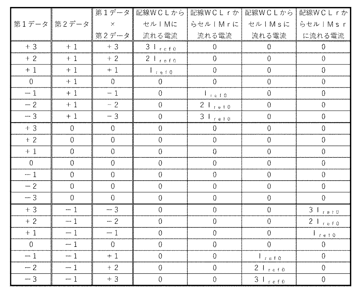
以上のとおり、演算回路MAC2を用いることによって、正、負、又は“0”の第1データと、正、又は“0”の第2データとの積和演算を行うことができる。また、演算回路MAC3を用いることによって、正、負、又は“0”の第1データと、正、負、又は“0”の第2データと、の積和演算を行うことができる。
なお、本発明の一態様は、本実施の形態で述べた演算回路MAC2、及び演算回路MAC3の回路構成に限定されない。演算回路MAC2、及び演算回路MAC3は、状況に応じて、回路構成を変更することができる。例えば、演算回路MAC3に含まれている、容量C5、容量C5r、容量C5s、容量C5sr、容量C5m、及び容量C5msは、トランジスタのゲート容量とすることができる(図示しない)。また、演算回路MAC3において、ノードNN、ノードNNr、ノードNNs、ノードNNsr、ノードNNref、及びノードNNrefsと周辺の配線との寄生容量が大きい場合は、容量C5、容量C5r、容量C5s、容量C5sr、容量C5m、及び容量C5msは、必ずしも設けなくてもよい。
なお、本実施の形態は、本明細書等で示す他の実施の形態等と適宜組み合わせることができる。
(実施の形態4)
本実施の形態では、階層型のニューラルネットワークについて説明する。なお、階層型のニューラルネットワークの演算は、上記の実施の形態で説明した半導体装置を用いることによって行うことができる。
本実施の形態では、階層型のニューラルネットワークについて説明する。なお、階層型のニューラルネットワークの演算は、上記の実施の形態で説明した半導体装置を用いることによって行うことができる。
<階層型のニューラルネットワーク>
階層型のニューラルネットワークは、一例としては、一の入力層と、一又は複数の中間層(隠れ層)と、一の出力層と、を有し、合計3以上の層によって構成されている。図19Aに示す階層型のニューラルネットワーク100はその一例を示しており、ニューラルネットワーク100は、第1層乃至第R層(ここでのRは4以上の整数とすることができる。)を有している。特に、第1層は入力層に相当し、第R層は出力層に相当し、それら以外の層は中間層に相当する。なお、図19Aには、中間層として第(k−1)層、第k層(ここでのkは3以上R−1以下の整数とする。)を図示しており、それ以外の中間層については図示を省略している。
階層型のニューラルネットワークは、一例としては、一の入力層と、一又は複数の中間層(隠れ層)と、一の出力層と、を有し、合計3以上の層によって構成されている。図19Aに示す階層型のニューラルネットワーク100はその一例を示しており、ニューラルネットワーク100は、第1層乃至第R層(ここでのRは4以上の整数とすることができる。)を有している。特に、第1層は入力層に相当し、第R層は出力層に相当し、それら以外の層は中間層に相当する。なお、図19Aには、中間層として第(k−1)層、第k層(ここでのkは3以上R−1以下の整数とする。)を図示しており、それ以外の中間層については図示を省略している。
ニューラルネットワーク100の各層は、一又は複数のニューロンを有する。図19Aにおいて、第1層はニューロンN1
(1)乃至ニューロンNp
(1)(ここでのpは1以上の整数である。)を有し、第(k−1)層はニューロンN1
(k−1)乃至ニューロンNm
(k−1)(ここでのmは1以上の整数である。)を有し、第k層はニューロンN1
(k)乃至ニューロンNn
(k)(ここでのnは1以上の整数である。)を有し、第R層はニューロンN1
(R)乃至ニューロンNq
(R)(ここでのqは1以上の整数である。)を有する。
なお、図19Aには、ニューロンN1
(1)と、ニューロンNp
(1)と、ニューロンN1
(k−1)と、ニューロンNm
(k−1)と、ニューロンN1
(k)と、ニューロンNn
(k)と、ニューロンN1
(R)と、ニューロンNq
(R)と、に加えて、第(k−1)層のニューロンNi
(k−1)(ここでのiは1以上m以下の整数である。)と、第k層のニューロンNj
(k)(ここでのjは1以上n以下の整数である。)と、も図示しており、それ以外のニューロンについては図示を省略している。
次に、前層のニューロンから次層のニューロンへの信号の伝達、及びそれぞれのニューロンにおいて入出力される信号について説明する。なお、本説明では、第k層のニューロンNj
(k)に着目する。
図19Bには、第k層のニューロンNj
(k)と、ニューロンNj
(k)に入力される信号と、ニューロンNj
(k)から出力される信号と、を示している。
具体的には、第(k−1)層のニューロンN1
(k−1)乃至ニューロンNm
(k−1)のそれぞれの出力信号であるz1
(k−1)乃至zm
(k−1)(代表して、z1
(k−1)、zi
(k−1)(iを1以上m以下の整数とする。)、及びzm
(k−1)を図示している。)が、ニューロンNj
(k)に向けて出力されている。そして、ニューロンNj
(k)は、z1
(k−1)乃至zm
(k−1)に応じてzj
(k)を生成して、zj
(k)を出力信号として第(k+1)層(図示しない。)の各ニューロンに向けて出力する。
前層のニューロンから次層のニューロンに入力される信号は、それらのニューロン同士を接続する結合強度(以後、重み係数と呼称する。)によって、信号の伝達の度合いが定まる。ニューラルネットワーク100では、前層のニューロンから出力された信号は、対応する重み係数を乗じられて、次層のニューロンに入力される。第(k−1)層のニューロンNi
(k−1)と第k層のニューロンNj
(k)とを接続する重み係数をwi
(k−1)
j
(k)としたとき、第k層のニューロンNj
(k)に入力される信号は、式(5.1)で表すことができる。

つまり、第(k−1)層のニューロンN1
(k−1)乃至ニューロンNm
(k−1)のそれぞれから第k層のニューロンNj
(k)に信号が伝達するとき、当該信号であるz1
(k−1)乃至zm
(k−1)には、それぞれの信号に対応する重み係数(w1
(k−1)
j
(k)乃至wm
(k−1)
j
(k))が乗じられる。そして、第k層のニューロンNj
(k)には、w1
(k−1)
j
(k)・z1
(k−1)乃至wm
(k−1)
j
(k)・zm
(k−1)が入力される。このとき、第k層のニューロンNj
(k)に入力される信号の総和uj
(k)は、式(5.2)となる。

また、重み係数w1
(k−1)
j
(k)乃至wm
(k−1)
j
(k)と、ニューロンの信号z1
(k−1)乃至zm
(k−1)と、の積和の結果には、偏りとしてバイアスを与えてもよい。バイアスをbとしたとき、式(5.2)は、次の式に書き直すことができる。

ニューロンNj
(k)は、uj
(k)に応じて、出力信号zj
(k)を生成する。ここで、ニューロンNj
(k)からの出力信号zj
(k)を次の式で定義する。

関数f(uj
(k))は、階層型のニューラルネットワークにおける活性化関数であり、例えば、ステップ関数、線形ランプ関数、又はシグモイド関数などを用いることができる。なお、活性化関数は、全てのニューロンにおいて同一でもよいし、又は異なっていてもよい。加えて、ニューロンの活性化関数は、層毎において、同一でもよいし、異なっていてもよい。
ところで、各層のニューロンが出力する信号、重み係数w、及びバイアスbのそれぞれは、アナログ値としてもよいし、デジタル値としてもよい。デジタル値としては、例えば、2値としてもよいし、3値としてもよい。さらに大きなビット数の値でもよい。例えば、アナログ値の場合、活性化関数として、線形ランプ関数、又はシグモイド関数などを用いればよい。例えば、デジタル値の2値の場合、出力を−1若しくは1、又は、0若しくは1、とするステップ関数を用いればよい。また、各層のニューロンが出力する信号は3値以上としてもよく、この場合、活性化関数は3値を出力する関数、例えば、出力を−1、0、若しくは1とするステップ関数、又は、出力を0、1、若しくは2とするステップ関数、などを用いればよい。また、例えば、5値を出力する活性化関数として、出力を−2、−1、0、1、若しくは2とするステップ関数などを用いてもよい。各層のニューロンが出力する信号、重み係数w、及びバイアスbの少なくとも一つについて、デジタル値を用いることにより、例えば、回路規模を小さくすること、消費電力を低減すること、又は、演算スピードを速くすること、などが出来る。また、各層のニューロンが出力する信号、重み係数w、及びバイアスbの少なくとも一つについて、アナログ値を用いることにより、演算の精度を向上させることが出来る。
ニューラルネットワーク100は、第1層(入力層)に入力信号が入力されることによって、第1層(入力層)から最後の層(出力層)までの各層において順次に、前層から入力された信号を基に、式(5.1)、式(5.2)(又は式(5.3))、及び式(5.4)を用いて出力信号を生成して、当該出力信号を次層に出力する動作を行う。最後の層(出力層)から出力された信号が、ニューラルネットワーク100によって計算された結果に相当する。
実施の形態2で述べた演算回路MAC1を、上述した隠れ層として適用する場合、重み係数ws[k−1]
(k−1)
s[k]
(k)(s[k−1]は1以上m以下の整数とし、s[k]は1以上n以下の整数とする)を第1データとして、第1データに応じた電流量を同じ列の各セルIMに順次記憶させて、第(k−1)層のニューロンNs[k−1]
(k−1)からの出力信号zs[k−1]
(k−1)を第2データとして、第2データに応じた電流量を回路XCSから各行の配線XCLに対して流すことで、変換回路ITRZに入力される電流量ISから第1データと第2データとの積和を求めることができる。加えて、当該積和の値を用いて活性化関数の値を求めることによって、活性化関数の値を信号として第k層のニューロンNs[k]
(k)の出力信号zs[k]
(k)とすることができる。
また、実施の形態2で述べた演算回路MAC1を、上述した出力層として適用する場合、重み係数ws[R−1]
(R−1)
s[R]
(R)(s[R−1]は1以上の整数とし、s[R]は1以上q以下の整数とする)を第1データとして、第1データに応じた電流量を同じ列の各セルIMに順次記憶させて、第(R−1)層のニューロンNs[R−1]
(R−1)からの出力信号zs[R−1]
(R−1)を第2データとして、第2データに応じた電流量を回路XCSから各行の配線XCLに対して流すことで、変換回路ITRZに入力される電流量ISから、第1データと第2データとの積和を求めることができる。加えて、当該積和の値を用いて活性化関数の値を求めることによって、活性化関数の値を信号として第R層のニューロンNs[R]
(R)の出力信号zs[R]
(R)とすることができる。
なお、本実施の形態で述べた入力層は、入力信号を第2層に出力するバッファ回路として機能してもよい。
また、実施の形態3で述べた、変換回路ITRZD[j]を図15の変換回路ITRZD4とした演算回路MAC2を、上述した隠れ層として適用する場合、重み係数ws[k−1]
(k−1)
s[k]
(k)を第1データとして、第1データに応じた電流量を同じ列の各回路CESのセルIMとセルIMrに順次記憶させて、第(k−1)層のニューロンNs[k−1]
(k−1)からの出力信号zs[k−1]
(k−1)を第2データとして、第2データに応じた電流量を回路XCSから各行の配線XCLに対して流すことで、変換回路ITRZD4に入力される電流量IS、及びISrから第1データと第2データとの積和に応じた活性化関数の値を算出することができる。つまり、当該値を信号として第k層のニューロンNs[k]
(k)の出力信号zs[k]
(k)とすることができる。また、変換回路ITRZD4は、当該値に応じた電流量を出力する構成となっているため、例えば、第(k+1)層の複数のニューロンに入力される、第k層のニューロンNs[k]
(k)の出力信号zs[k]
(k)は、電流とすることができる。つまり、第(k+1)層の隠れ層として演算回路MAC2を適用する場合、演算回路MAC2の配線XCLに入力される第k層のニューロンNs[k]
(k)の出力信号zs[k]
(k)は、回路XCSで生成せず、第k層の隠れ層の演算回路MAC2の変換回路ITRZD4から出力された電流とすることができる。
具体的には、図20に示す演算回路を用いることによって、上述した階層型のニューラルネットワークの演算を行うことができる。図20の演算回路は、一例として、図13の演算回路MAC2と同様の構成の演算回路MAC2−1と、図13の演算回路MAC2において回路XCSを設けていない構成の演算回路MAC2−2と、を有する。なお、演算回路MAC2−1のセルアレイCAには、m×n個の回路CESがマトリクス状に配置され、演算回路MAC2−2のセルアレイCAには、n×t個(tは1以上の整数とする。)の回路CESがマトリクス状に配置されている。また、演算回路MAC2−1の配線OL[1]乃至配線OL[n]のそれぞれは、演算回路MAC2−2の配線XCL[1]乃至配線XCL[n]に電気的に接続されている。なお、図20には、代表して、演算回路MAC2−1が有する回路CES[1,1]、回路CES[1,n]、回路CES[m,1]、回路CES[m,n]、変換回路ITRZD4[1]、変換回路ITRZD4[n]、配線OL[1]、及び配線OL[n]などを示している。また、演算回路MAC2−2が有する回路CES[1,1]、回路CES[1,t]、回路CES[n,1]、回路CES[n,t]、変換回路ITRZD4[1]、変換回路ITRZD4[t]、配線OL[1]、及び配線OL[t]などを示している。また、回路CES[1,1]が有するセルIM[1,1]及びセルIMr[1,1]と、回路CES[1,n]が有するセルIM[1,n]及びセルIMr[1,n]と、回路CES[m,1]が有するセルIM[m,1]及びセルIMr[m,1]と、回路CES[m,n]が有するセルIM[m,n]及びセルIMr[m,n]と、回路CES[1,t]が有するセルIM[1,t]及びセルIMr[1,t]と、回路CES[n,1]が有するセルIM[n,1]及びセルIMr[n,1]と、回路CES[n,t]が有するセルIM[n,t]及びセルIMr[n,t]と、を示している。
例えば、図20の演算回路MAC2−1で、第(k−1)層のニューロンと第k層のニューロンとの間の重み係数を第1データとして、セルアレイCAの回路CES[1,1]乃至回路CES[m,n]に保持し、第(k−1)層のニューロンNs[k−1]
(k−1)からの出力信号zs[k−1]
(k−1)を第2データとして、第2データに応じた電流量を回路XCSから各行の配線XCLに対して流すことで、配線OL[1]乃至配線OL[n]のそれぞれから第k層のニューロンN1
(k)乃至ニューロンNn
(k)の出力信号z1
(k)乃至zn
(k)を出力することができる。なお、出力信号z1
(k)乃至zn
(k)のそれぞれの値は、変換回路ITRZD4[1]乃至変換回路ITRZD4[n]から出力される電流の量として表すことができる。
ここで、図20の演算回路MAC2−2で、第k層のニューロンと第(k+1)層のニューロンとの間の重み係数を第1データとして、セルアレイCAの回路CES[1,1]乃至回路CES[n,t]に保持し、各行の配線XCLに流れる電流量、すなわち第k層のニューロンN1
(k)乃至ニューロンNn
(k)の出力信号z1
(k)乃至zn
(k)を第2データとすることで、配線OL[s[k+1]](ここでのs[k+1]は1以上t以下の整数とする)から第(k+1)層のニューロンNs[k+1]
(k+1)の出力信号zs[k+1]
(k+1)を出力することができる。
ところで、実施の形態3で説明したとおり、図20の演算回路MAC2−1の変換回路ITRZD4[1]乃至変換回路ITRZD4[n]に、図15、図16A、図17A乃至図17Cのいずれか一の変換回路ITRZD4を適用することで、変換回路ITRZD4[1]乃至変換回路ITRZD4[n]はReLU関数として作用する。そのため、例えば、回路CES[1,j]乃至回路CES[m,j]における積和演算の結果が“負”であるとき、変換回路ITRZD4から配線OL[j]に流れる電流量は、理想的には0となることが好ましい。しかし、実際には、変換回路ITRZD4から配線OL[j]に微小の電流量が流れる、又は配線OL[j]から変換回路ITRZD4に微小の電流量が流れる場合がある。
そのため、階層型のニューラルネットワークの次層以降の演算を適切に行うための演算回路MAC2−2の構成例を図21に示す。図21に示す演算回路MAC2−2は、図13の演算回路MAC2においてセルアレイCAに配置されている回路CESを、m×nのマトリクス状からn×tのマトリクス状に変更し、かつ回路XCSを設けていない構成となっている。また、演算回路MAC2−2のセルアレイCAの回路CESは、n×tのマトリクス状に配置されているため、図21において、例えば、配線及び回路などの符号に付与している[ ]などの括弧内の値も変更している。図21には、回路CES[1,h](hは1以上t以下の整数である。)、回路CES[n,h]、及び変換回路ITRZD[h]を示している。また、トランジスタF3[h]、トランジスタF3r[h]、トランジスタF4[h]、及びトランジスタF4r[h]を示している。また、配線WCL[h]、配線WCLr[h]、配線WSL[1]、配線WSL[n]、及び配線OL[h]を示している。また、ノードNN[1,h]、ノードNN[n,h]、ノードNNr[1,h]、ノードNNr[n,h]、ノードNNref[1]、及びノードNNref[n]を示している。
さらに、図21の演算回路MAC2−2では、一例として、演算回路MAC2−2に、配線TM[1]、配線TM[n]、配線TH[1,h]、配線TH[n,h]、配線THr[1,h]、及び配線THr[n,h]を設けた回路構成の例を示している。図21の演算回路MAC2−2において、セルIMref[1]のトランジスタF2mのバックゲートには配線TM[1]が電気的に接続され、セルIMref[n]のトランジスタF2mのバックゲートには配線TM[n]が電気的に接続され、セルIM[1,h]のトランジスタF2のバックゲートには配線TH[1,h]が電気的に接続され、セルIMr[1,h]のトランジスタF2rのバックゲートには配線THr[1,h]が電気的に接続され、セルIM[n,h]のトランジスタF2のバックゲートには配線TH[n,h]が電気的に接続され、セルIMr[n,h]のトランジスタF2rのバックゲートには配線THr[n,h]が電気的に接続されている。
配線TM[1]、配線TM[n]、配線TH[1,h]、配線TH[n,h]、配線THr[1,h]、及び配線THr[n,h]のそれぞれに低レベル電位を与えることによって、それぞれの配線に電気的に接続されているバックゲートを有するトランジスタのしきい値電圧を高くすることができる。これにより、演算回路MAC2−1の配線OLに流れる微小の電流量が、演算回路MAC2−2のセルIMrefを介して、配線VEに流れることを防ぐことができる。つまり、変換回路ITRZD4[1]乃至変換回路ITRZD4[n]における出力特性を、ReLU関数に近づけることができる。そのため、階層型のニューラルネットワークの次層の演算を適切に行うことができる。
また、例えば、図21の演算回路MAC2−2の構成を、図20の演算回路MAC2−1に適用してもよい。このような構成にすることによって、演算回路MAC2−2と同様に、演算回路MAC2−1に含まれているトランジスタF2とトランジスタF2rとトランジスタF2mとのそれぞれのしきい値電圧も変動させることができる。
なお、図21では、配線TM[1]、配線TM[n]、配線TH[1,h]、配線TH[n,h]、配線THr[1,h]、及び配線THr[n,h]を図示しているが、図21の演算回路MAC2−2は、例えば、配線TM[1]と配線TH[1,h]と配線THr[1,h]とを1本の配線としてまとめ、かつ配線TM[n]と配線TH[n,h]と配線THr[n,h]とを1本の配線としてまとめた構成としてもよい。
上述した通り、階層型のニューラルネットワークの演算を、図20に示す演算回路を構成することにより、演算回路MAC2−1で出力したニューロンの出力信号の値(電流量)をそのまま演算回路MAC2−2に入力することができるため、階層型のニューラルネットワークの演算を、一例として、第1層から連続して行うことができる。また、演算回路MAC2−1の配線OL[1]乃至配線OL[n]から出力された出力信号を、例えば外部回路などによって一時的に記憶する必要が無いため、一時記憶に必要な記憶装置を別途設けなくてもよい。つまり、図20の演算回路を構成することによって、回路面積を低減することができ、また、一時記憶のためのデータ送信に必要な電力を低減することができる。
なお、本実施の形態は、本明細書等で示す他の実施の形態等と適宜組み合わせることができる。
(実施の形態5)
本実施の形態では、上記の実施の形態で説明した半導体装置を、積層した構成の一例について説明する。
本実施の形態では、上記の実施の形態で説明した半導体装置を、積層した構成の一例について説明する。
図22は、積和演算、及び関数系の演算を連続して実行することができる演算回路の一例を示したブロック図である。図22に示す回路CDVは、一例として、演算回路MACL[1]乃至演算回路MACL[4]を有する。なお、本明細書等において、演算回路MACL[1]乃至演算回路MACL[4]のそれぞれは、「層」、「演算層」、又は「回路層」と言い換えることができるものとする。また、演算回路MACL[1]乃至演算回路MACL[4]のそれぞれに共通する事項を説明する場合、単に演算回路MACLと記載する場合がある。
回路CDVにおいて、演算回路MACL[2]は、演算回路MACL[1]の上方に位置し、演算回路MACL[3]は、演算回路MACL[2]の上方に位置し、演算回路MACL[4]は、演算回路MACL[3]の上方に位置している。
なお、図22では、演算回路MACLが4個積層された構成を示しているが、回路CDVの構成は、演算回路MACLが2個又は3個積層された構成としてもよい。又は、回路CDVの構成は、演算回路MACLが5個以上積層された構成としてもよい。
演算回路MACL[1]乃至演算回路MACL[4]のそれぞれは、セルアレイCAと、回路WCSと、回路ITSと、を有する。また、演算回路MACL[1]は、回路XCSを有する。なお、図22には、演算回路MACL[2]乃至演算回路MACL[4]のそれぞれに回路XCSが含まれていない構成を示しているが、演算回路MACL[2]乃至演算回路MACL[4]のそれぞれは、回路XCSを有してもよい。
回路WCSは、一例として、外部から与えられたデジタルデータである第1データ(ニューラルネットワークの場合、重み係数に相当する)をアナログデータ(電流)に変換する機能を有する。
回路XCSは、一例として、外部から与えられたデジタルデータである第2データ(ニューラルネットワークの場合、入力データに相当する)をアナログデータ(電流)に変換する機能を有する。
セルアレイCAは、一例として、乗算を行う演算セルを複数有する。なお、演算セルは、例えば、セルアレイCAの内部において、アレイ状に配置されている。また、セルアレイCAは、第1データと第2データとの積和演算を行って、その結果を電流量として出力する機能を有する。
回路ITSは、セルアレイCAから出力された積和演算の結果(電流)を取得して、関数系の演算を行う機能を有する。また、回路ITSは、当該演算の結果を外部に出力する機能を有する。
なお、回路WCS、回路XCS、セルアレイCA、及び回路ITSのそれぞれの詳細については、上述した実施の形態2及び実施の形態3を適宜参酌することができる。
次に、回路CDVに入力されるデータ、回路CDVの内部で演算されるデータ、及び回路CDVから出力されるデータについて説明する。なお、図22において、ハッチングを有する矢印は、デジタルデータを示し、白色の矢印は、アナログデータを示す。
演算回路MACL[1]において、回路WCSにデジタルデータの第1データW(1)が入力される。これにより、回路WCSは、第1データW(1)をアナログデータ(電流)として、セルアレイCAに入力する。なお、W(1)は行列とすることができる。
また、演算回路MACL[1]において、回路XCSにデジタルデータの第2データX(1)が入力される。これにより、回路XCSは、第2データX(1)をアナログデータ(電流)として、セルアレイCAに入力する。なお、X(1)は行列とすることができる。
演算回路MACL[1]のセルアレイCAは、第1データW(1)と第2データX(1)との積和演算を実行して、X(1)W(1)に応じた量の電流を出力する。また、当該電流は、回路ITSに入力される。
演算回路MACL[1]の回路ITSは、X(1)W(1)に応じた量の電流を取得することによって、F(X(1)W(1))に応じた量の電流を出力する。なお、F(x)は、回路ITSで演算を行う関数であり、特に、F(X(1)W(1))=X(2)として定義する。なお、X(2)は行列とすることができる。また、F(X(1)W(1))=X(2)に応じた量の電流は、演算回路MACL[2]のセルアレイCAに流れる。
演算回路MACL[2]において、回路WCSにデジタルデータの第1データW(2)が入力される。これにより、回路WCSは、第1データW(2)をアナログデータ(電流)として、セルアレイCAに入力する。なお、W(2)は行列とすることができる。
演算回路MACL[2]のセルアレイCAは、第1データW(2)と第2データX(2)との積和演算を実行して、X(2)W(2)に応じた量の電流を出力する。また、当該電流は、回路ITSに入力されて、回路ITSによって、F(X(2)W(2))=X(3)に応じた量の電流を出力する。
演算回路MACL[3]についても、演算回路MACL[1]、及び演算回路MACL[2]と同様に、回路WCSにデジタルデータであるW(3)を入力することによって、セルアレイCAにおいて、X(3)W(3)の演算が行われ、回路ITSからF(X(3)W(3))=X(4)に応じた量の電流が出力される。
演算回路MACL[4]についても、演算回路MACL[1]乃至演算回路MACL[3]と同様に、回路WCSにデジタルデータであるW(4)を入力することによって、セルアレイCAにおいて、X(4)W(4)の演算が行われる。また、演算回路MACL[4]の回路ITSでは、F(X(4)W(4))=Tに応じた量の電流が出力される。なお、Tは、回路CDVにおける出力データであって、行列とすることができる。
演算回路MACL[1]乃至演算回路MACL[4]は、例えば、OSトランジスタを用いて構成することが好ましい。OSトランジスタは、平坦性の高い膜上であれば、Siトランジスタと比較して容易に形成することができるため、図22に示すような演算回路MACL[1]乃至演算回路MACL[4]の積層構造を作製することができる。
また、図22の回路CDVは、下方の演算回路MACL[1]から上方の演算回路MACL[4]にかけて、連続して演算を行う構成となっているが、演算の流れは、例えば、上方に位置する演算回路MACLから下方に位置する演算回路MACLにかけて、演算が行われてもよい。つまり、回路CDVは、演算回路MACL[1]が、演算回路MACL[2]の上方に位置し、演算回路MACL[2]が、演算回路MACL[3]の上方に位置し、演算回路MACL[3]が、演算回路MACL[4]の上方に位置する構成としてもよい。
上記のとおり、回路CDVを、演算回路MACL[1]乃至演算回路MACL[4]を積層した構成とすることによって、回路規模が低減された半導体装置とすることができる。また、回路CDVを階層型のニューラルネットワークのモデルとして構築する場合、演算回路MACL[1]乃至演算回路MACL[4]のそれぞれのセルアレイCAには、第1データとして各階層に応じた重み係数を書き込めばよい。これにより、ニューラルネットワークの演算中において、演算回路MACL[1]乃至演算回路MACL[4]のそれぞれのセルアレイCAで重み係数の書き換えの必要が無くなるため、ニューラルネットワークの演算に必要な消費電力を従来よりも低くすることができる。
なお、本実施の形態は、本明細書等で示す他の実施の形態等と適宜組み合わせることができる。
(実施の形態6)
本実施の形態では、チャネル形成領域に酸化物半導体を含むトランジスタ(OSトランジスタ)について、説明する。なお、OSトランジスタの説明において、チャネル形成領域にシリコンを含むトランジスタ(Siトランジスタともいう)との比較についても簡単に説明する。
本実施の形態では、チャネル形成領域に酸化物半導体を含むトランジスタ(OSトランジスタ)について、説明する。なお、OSトランジスタの説明において、チャネル形成領域にシリコンを含むトランジスタ(Siトランジスタともいう)との比較についても簡単に説明する。
〔OSトランジスタ〕
OSトランジスタには、キャリア濃度の低い酸化物半導体を用いることが好ましい。例えば、酸化物半導体のチャネル形成領域のキャリア濃度は、1×1018cm−3以下、好ましくは1×1017cm−3未満、より好ましくは1×1016cm−3未満、さらに好ましくは1×1013cm−3未満、さらに好ましくは1×1010cm−3未満であり、かつ、1×10⁻⁹cm−3以上である。なお、酸化物半導体中のキャリア濃度を低くする場合、当該酸化物半導体中の不純物濃度を低くすることで、当該酸化物半導体中の欠陥準位密度を低くすればよい。本明細書等において、不純物濃度が低く、欠陥準位密度の低いことを、高純度真性または実質的に高純度真性という。なお、キャリア濃度の低い酸化物半導体を、高純度真性または実質的に高純度真性な酸化物半導体と呼ぶ場合がある。
OSトランジスタには、キャリア濃度の低い酸化物半導体を用いることが好ましい。例えば、酸化物半導体のチャネル形成領域のキャリア濃度は、1×1018cm−3以下、好ましくは1×1017cm−3未満、より好ましくは1×1016cm−3未満、さらに好ましくは1×1013cm−3未満、さらに好ましくは1×1010cm−3未満であり、かつ、1×10⁻⁹cm−3以上である。なお、酸化物半導体中のキャリア濃度を低くする場合、当該酸化物半導体中の不純物濃度を低くすることで、当該酸化物半導体中の欠陥準位密度を低くすればよい。本明細書等において、不純物濃度が低く、欠陥準位密度の低いことを、高純度真性または実質的に高純度真性という。なお、キャリア濃度の低い酸化物半導体を、高純度真性または実質的に高純度真性な酸化物半導体と呼ぶ場合がある。
また、高純度真性または実質的に高純度真性である酸化物半導体は、欠陥準位密度が低いため、トラップ準位密度も低くなる場合がある。また、酸化物半導体のトラップ準位に捕獲された電荷は、消失するまでに要する時間が長く、あたかも固定電荷のように振る舞うことがある。そのため、トラップ準位密度の高い酸化物半導体にチャネル形成領域が形成されるトランジスタは、電気特性が不安定となる場合がある。
したがって、トランジスタの電気特性を安定にするためには、酸化物半導体中の不純物濃度を低減することが有効である。また、酸化物半導体中の不純物濃度を低減するためには、近接する膜中の不純物濃度も低減することが好ましい。不純物としては、例えば水素または窒素などが挙げられる。なお、酸化物半導体中の不純物とは、例えば、酸化物半導体を構成する主成分以外をいう。例えば、濃度が0.1原子%未満の元素は不純物といえる。
また、OSトランジスタは、酸化物半導体中のチャネル形成領域に不純物または酸素欠損が存在すると、電気特性が変動しやすく、信頼性が悪くなる場合がある。また、OSトランジスタは、酸化物半導体中の酸素欠損に水素が入った欠陥(以下、VOHと呼ぶ場合がある)を形成し、キャリアとなる電子を生成する場合がある。また、OSトランジスタは、チャネル形成領域にVOHが形成されると、チャネル形成領域中のドナー濃度が増加する場合がある。これによって、OSトランジスタは、チャネル形成領域中のドナー濃度が増加するにつれ、しきい値電圧がばらつくことがある。このため、OSトランジスタは、酸化物半導体中のチャネル形成領域に酸素欠損が含まれていると、ノーマリーオン特性(ゲート電圧が0Vの時にドレイン電流が流れる特性)となりやすい。したがって、酸化物半導体中のチャネル形成領域では、不純物、酸素欠損、およびVOHは、できる限り低減されていることが好ましい。
また、酸化物半導体のバンドギャップは、シリコンのバンドギャップ(代表的には1.1eV)よりも大きいことが好ましく、好ましくは2eV以上、より好ましくは2.5eV以上、さらに好ましくは3.0eV以上である。シリコンよりも、バンドギャップの大きい酸化物半導体を用いることで、トランジスタのオフ電流(Ioffとも呼称する)を低減することができる。
また、Siトランジスタでは、トランジスタの微細化が進むにつれて、短チャネル効果(SCE:Short Channel Effect)が発現する。そのため、Siトランジスタでは、微細化が困難となる。短チャネル効果が発現する要因の一つとして、シリコンのバンドギャップが小さいことが挙げられる。一方、OSトランジスタは、バンドギャップの大きい半導体材料である、酸化物半導体を用いるため、短チャネル効果の抑制を図ることができる。別言すると、OSトランジスタは、短チャネル効果がない、または短チャネル効果が極めて少ないトランジスタである。
なお、短チャネル効果とは、トランジスタの微細化(チャネル長の縮小)に伴って顕在化する電気特性の劣化である。短チャネル効果の具体例としては、例えば、しきい値電圧の低下、サブスレッショルドスイング値(S値と表記することがある)の増大、および漏れ電流の増大などがある。ここで、S値とは、サブスレッショルド領域において、ドレイン電圧が一定で、ドレイン電流を1桁変化させる際の、ゲート電圧の変化量をいう。
また、短チャネル効果に対する耐性の指標として、特性長(Characteristic Length)が広く用いられている。特性長とは、チャネル形成領域のポテンシャルの曲がりやすさの指標である。特性長が小さいほどポテンシャルが急峻に立ち上がるため、短チャネル効果に強いといえる。
OSトランジスタは蓄積型のトランジスタであり、Siトランジスタは反転型のトランジスタである。したがって、OSトランジスタは、Siトランジスタと比較して、ソース領域−チャネル形成領域間の特性長、およびドレイン領域−チャネル形成領域間の特性長が小さい。したがって、OSトランジスタは、Siトランジスタよりも短チャネル効果に強い。すなわち、チャネル長の短いトランジスタを作製したい場合においては、OSトランジスタは、Siトランジスタよりも好適である。
チャネル形成領域がi型または実質的にi型となるまで酸化物半導体のキャリア濃度を下げた場合においても、短チャネルのトランジスタでは、Conduction−Band−Lowering(CBL)効果により、チャネル形成領域の伝導帯下端が下がるため、ソース領域またはドレイン領域と、チャネル形成領域と、の間の伝導帯下端のエネルギー差は、0.1eV以上0.2eV以下まで小さくなる可能性がある。これにより、OSトランジスタは、チャネル形成領域がn−型の領域となり、ソース領域およびドレイン領域のそれぞれがn+型の領域となる、n+/n−/n+の蓄積型junction−lessトランジスタ構造、または、n+/n−/n+の蓄積型non−junctionトランジスタ構造、と捉えることもできる。
OSトランジスタは、上記の構造とすることで、微細化または高集積化しても、良好な電気特性を有することができる。例えば、OSトランジスタは、ゲート長が、20nm以下、15nm以下、10nm以下、7nm以下、または6nm以下であって、かつ、1nm以上、3nm以上、または5nm以上であっても、良好な電気特性を得ることができる。一方で、Siトランジスタは、短チャネル効果が発現するため、20nm以下、または15nm以下のゲート長とすることが困難な場合がある。したがって、OSトランジスタは、Siトランジスタと比較して、チャネル長の短いトランジスタに好適に用いることができる。なお、ゲート長とは、トランジスタ動作時にキャリアがチャネル形成領域内部を移動する方向における、ゲート電極の長さであり、トランジスタの平面視における、ゲート電極の底面の幅をいう。
また、OSトランジスタを微細化することで、トランジスタの高周波特性を向上させることができる。具体的には、トランジスタの遮断周波数を向上させることができる。OSトランジスタのゲート長が上記範囲のいずれかである場合、トランジスタの遮断周波数を、例えば室温環境下で、50GHz以上、好ましくは100GHz以上、さらに好ましくは150GHz以上とすることができる。
以上の説明の通り、OSトランジスタは、Siトランジスタと比較し、オフ電流が小さい、かつ、チャネル長の短いトランジスタの作製が可能である、といった優れた効果を有する。
本実施の形態に示す構成、構造、または方法等は、他の実施の形態等に示す構成、構造、または方法等と適宜組み合わせて用いることができる。
(実施の形態7)
本実施の形態では、上記実施の形態で説明した半導体装置を用いることができる、電子部品、電子機器、大型計算機、宇宙用機器、およびデータセンター(Data Center:DCとも呼称する)について説明する。本発明の一態様の半導体装置を用いた、電子部品、電子機器、大型計算機、宇宙用機器、およびデータセンターは、低消費電力化といった高性能化に有効である。
本実施の形態では、上記実施の形態で説明した半導体装置を用いることができる、電子部品、電子機器、大型計算機、宇宙用機器、およびデータセンター(Data Center:DCとも呼称する)について説明する。本発明の一態様の半導体装置を用いた、電子部品、電子機器、大型計算機、宇宙用機器、およびデータセンターは、低消費電力化といった高性能化に有効である。
〔電子部品〕
図23Aは、電子部品700および電子部品700が実装された基板(実装基板704)の斜視図である。図23Aに示す電子部品700は、モールド711内に半導体装置710を有している。図23Aは、電子部品700の内部を示すために、一部の記載を省略している。電子部品700は、モールド711の外側にランド712を有する。ランド712は、電極パッド713と電気的に接続されている。電極パッド713は、ワイヤ714によって、半導体装置710と電気的に接続されている。電子部品700は、例えば、プリント基板702に実装される。このような電子部品が複数組み合わされて、それぞれの電子部品がプリント基板702上で電気的に接続されることで、実装基板704が完成する。
図23Aは、電子部品700および電子部品700が実装された基板(実装基板704)の斜視図である。図23Aに示す電子部品700は、モールド711内に半導体装置710を有している。図23Aは、電子部品700の内部を示すために、一部の記載を省略している。電子部品700は、モールド711の外側にランド712を有する。ランド712は、電極パッド713と電気的に接続されている。電極パッド713は、ワイヤ714によって、半導体装置710と電気的に接続されている。電子部品700は、例えば、プリント基板702に実装される。このような電子部品が複数組み合わされて、それぞれの電子部品がプリント基板702上で電気的に接続されることで、実装基板704が完成する。
また、半導体装置710は、駆動回路層715と、記憶層716と、を有する。なお、記憶層716は、複数のメモリセルアレイが積層された構成である。駆動回路層715と、記憶層716と、が積層された構成は、モノリシック積層の構成とすることができる。モノリシック積層の構成では、例えば、TSV(Through Silicon Via)などの貫通電極技術、および、Cu−Cu直接接合などの接合技術、を用いることなく、各層間を接続することができる。駆動回路層715と、記憶層716と、をモノリシック積層の構成とすることで、例えば、プロセッサ上にメモリが直接形成される、いわゆるオンチップメモリの構成とすることができる。オンチップメモリの構成とすることで、プロセッサと、メモリと、のインターフェース部分の動作を高速にすることが可能となる。
また、オンチップメモリの構成とすることで、例えば、TSVなどの貫通電極を用いる技術と比較し、接続配線などのサイズを小さくすることが可能であるため、接続ピン数を増加させることも可能となる。接続ピン数を増加させることで、並列動作が可能となるため、メモリのバンド幅(メモリバンド幅ともいう)を向上させることが可能となる。
また、記憶層716が有する複数のメモリセルアレイを、OSトランジスタを用いて形成し、当該複数のメモリセルアレイをモノリシックで積層することが好ましい。複数のメモリセルアレイをモノリシック積層の構成とすることで、メモリのバンド幅、およびメモリのアクセスレイテンシの、いずれか一または双方を向上させることができる。なお、バンド幅とは、単位時間あたりのデータ転送量である。また、アクセスレイテンシとは、アクセスしてからデータのやり取りが始まるまでの時間である。なお、記憶層716にSiトランジスタを用いる構成の場合、OSトランジスタと比較し、モノリシック積層の構成とすることが困難である。そのため、モノリシック積層の構成において、OSトランジスタは、Siトランジスタよりも優れた構造であるといえる。
すなわち、OSトランジスタは、Siトランジスタと比較し、広いメモリバンド幅の実現が可能である、といった優れた効果を有する。
なお、半導体装置710を、ダイと呼称してもよい。なお、本明細書等において、ダイとは、半導体チップの製造工程で、例えば円盤状の基板(ウエハともいう)などに回路パターンを形成し、さいの目状に切り分けて得られたチップ片を表す。なお、ダイに用いることのできる半導体材料として、例えば、シリコン、シリコンカーバイド、またはガリウムナイトライドなどが挙げられる。例えば、シリコン基板(シリコンウエハともいう)から得られたダイを、シリコンダイという場合がある。
図23Bは、電子部品730の斜視図である。電子部品730は、SiP(System in Package)またはMCM(Multi Chip Module)の一例である。電子部品730は、パッケージ基板732(プリント基板)上にインターポーザ731が設けられ、インターポーザ731上に半導体装置735、および複数の半導体装置710が設けられている。
電子部品730において、半導体装置710は、例えば、広帯域メモリ(HBM:High Bandwidth Memory)などの記憶装置として用いることができる。また、半導体装置735は、例えば、CPU(Central Processing Unit)、GPU(Graphics Processing Unit)、またはFPGA(Field Programmable Gate Array)などの集積回路(例えば、演算装置、制御装置、または信号処理装置など)として用いることができる。
パッケージ基板732は、例えば、セラミックス基板、プラスチック基板、またはガラスエポキシ基板などを用いることができる。インターポーザ731は、例えば、シリコンインターポーザ、または樹脂インターポーザなどを用いることができる。
インターポーザ731は、複数の配線を有し、当該複数の配線のそれぞれを介して、端子ピッチの異なる複数の集積回路のそれぞれを電気的に接続する機能を有する。複数の配線は、単層または多層で設けられる。また、インターポーザ731は、インターポーザ731上に設けられた集積回路と、パッケージ基板732に設けられた電極と、を電気的に接続する機能を有する。これらのことから、インターポーザ731を、「再配線基板」または「中間基板」と呼ぶ場合がある。また、インターポーザ731は、貫通電極を設けることで、当該貫通電極を用いて、集積回路と、パッケージ基板732と、を電気的に接続する場合もある。また、インターポーザ731は、シリコンインターポーザを用いる場合、貫通電極として、TSVを用いることもできる。
インターポーザ731は、シリコンインターポーザを用いることが好ましい。シリコンインターポーザは、能動素子を設ける必要が無いため、集積回路よりも低コストで作製することができる。また、シリコンインターポーザは、配線形成を半導体プロセスで行うことができるため、樹脂インターポーザでは難しい微細配線の形成が容易である。
HBMは、広いメモリバンド幅を実現するために、多くの配線を接続する必要がある。このため、HBMを実装するインターポーザは、微細かつ高密度の配線形成が求められる。よって、HBMを実装するインターポーザは、シリコンインターポーザを用いることが好ましい。
また、例えば、シリコンインターポーザを用いた、SiPまたはMCMなどは、集積回路とインターポーザとの間の膨張係数の違いによる信頼性の低下が生じにくい。また、シリコンインターポーザは、表面の平坦性が高いため、シリコンインターポーザ上に設ける集積回路とシリコンインターポーザとの間の接続不良が生じにくい。特に、インターポーザ上に複数の集積回路を横に並べて配置する2.5Dパッケージ(2.5次元実装)は、シリコンインターポーザを用いることが好ましい。
一方で、例えば、シリコンインターポーザ、およびTSVなどを用いて端子ピッチの異なる複数の集積回路を電気的に接続する場合、当該端子ピッチの幅などのスペースが必要となる。そのため、電子部品730のサイズを小さくしようとした場合、上記の端子ピッチの幅が問題になり、広いメモリバンド幅を実現するために必要な多くの配線を設けることが、困難になる場合がある。そこで、上述したように、OSトランジスタを用いたモノリシック積層の構成が好適である。TSVを用いて積層したメモリセルアレイと、モノリシック積層したメモリセルアレイと、を組み合わせた複合化構造としてもよい。
電子部品730を実装した基板は、電子部品730と重ねてヒートシンク(放熱板)を設けてもよい。ヒートシンクを設ける場合、インターポーザ731上に設ける集積回路は、高さを揃えることが好ましい。例えば、本実施の形態に示す電子部品730は、半導体装置710と半導体装置735との高さを揃えることが好ましい。
電子部品730を他の基板に実装するため、パッケージ基板732は、底部に電極733を設けてもよい。図23Bは、電極733を半田ボールで形成する例を示している。電子部品730は、パッケージ基板732の底部に半田ボールをマトリクス状に設けることで、BGA(Ball Grid Array)実装を実現できる。なお、電極733は、導電性のピンで形成してもよい。電子部品730は、パッケージ基板732の底部に導電性のピンをマトリクス状に設けることで、PGA(Pin Grid Array)実装を実現できる。
電子部品730は、BGAまたはPGAに限らず様々な実装方法を用いて他の基板に実装することができる。例えば、SPGA(Staggered Pin Grid Array)、LGA(Land Grid Array)、QFP(Quad Flat Package)、QFJ(Quad Flat J−leaded package)、またはQFN(Quad Flat Non−leaded package)などの実装方法を用いることができる。
〔電子機器〕
図24Aは、電子機器6500の斜視図である。図24Aに示す電子機器6500は、スマートフォンとして用いることのできる携帯情報端末機である。電子機器6500は、例えば、筐体6501、表示部6502、電源ボタン6503、ボタン6504、スピーカ6505、マイク6506、カメラ6507、光源6508、および制御装置6509などを有する。なお、制御装置6509としては、例えば、CPU、GPU、および記憶装置の中から選ばれるいずれか一または複数を有する。本発明の一態様の半導体装置は、例えば、表示部6502、または制御装置6509などに適用することができる。本発明の一態様の半導体装置を、制御装置6509に用いることで、消費電力を低減させることができるため好適である。
図24Aは、電子機器6500の斜視図である。図24Aに示す電子機器6500は、スマートフォンとして用いることのできる携帯情報端末機である。電子機器6500は、例えば、筐体6501、表示部6502、電源ボタン6503、ボタン6504、スピーカ6505、マイク6506、カメラ6507、光源6508、および制御装置6509などを有する。なお、制御装置6509としては、例えば、CPU、GPU、および記憶装置の中から選ばれるいずれか一または複数を有する。本発明の一態様の半導体装置は、例えば、表示部6502、または制御装置6509などに適用することができる。本発明の一態様の半導体装置を、制御装置6509に用いることで、消費電力を低減させることができるため好適である。
図24Bは、電子機器6600の斜視図である。図24Bに示す電子機器6600は、ノート型パーソナルコンピュータとして用いることのできる情報端末機である。電子機器6600は、例えば、筐体6611、キーボード6612、ポインティングデバイス6613、外部接続ポート6614、表示部6615、および制御装置6616などを有する。なお、制御装置6616としては、例えば、CPU、GPU、および記憶装置の中から選ばれるいずれか一または複数を有する。本発明の一態様の半導体装置は、例えば、制御装置6509、または制御装置6616などに適用することができる。本発明の一態様の半導体装置を、制御装置6616に用いることで、消費電力を低減させることができるため好適である。
〔大型計算機〕
図24Cは、大型計算機5600の斜視図である。図24Cに示す大型計算機5600には、ラック5610に、ラックマウント型の計算機5620が複数格納されている。なお、大型計算機5600を、スーパーコンピュータと呼称してもよい。
図24Cは、大型計算機5600の斜視図である。図24Cに示す大型計算機5600には、ラック5610に、ラックマウント型の計算機5620が複数格納されている。なお、大型計算機5600を、スーパーコンピュータと呼称してもよい。
図24Dは、計算機5620の構成例を説明する斜視図である。図24Dにおいて、計算機5620は、マザーボード5630を有する。マザーボード5630は、複数のスロット5631と、複数の接続端子(図示しない。)と、を有する。スロット5631には、PCカード5621が挿入されている。加えて、PCカード5621は、接続端子5623、接続端子5624、および接続端子5625を有し、それぞれ、マザーボード5630に接続されている。
図24Eに示すPCカード5621は、例えば、CPU、GPU、および記憶装置などを備えた処理ボードの一例である。PCカード5621は、ボード5622を有する。また、ボード5622は、接続端子5623と、接続端子5624と、接続端子5625と、半導体装置5626と、半導体装置5627と、半導体装置5628と、接続端子5629と、を有する。なお、図24Eには、半導体装置5626、半導体装置5627、および半導体装置5628以外の半導体装置を図示しているが、それらの半導体装置については、以下に記載する半導体装置5626、半導体装置5627、および半導体装置5628の説明を参酌すればよい。
接続端子5629は、マザーボード5630のスロット5631に挿入することができる形状を有しており、接続端子5629は、PCカード5621とマザーボード5630とを接続するためのインターフェースとして機能する。接続端子5629の規格としては、例えば、PCIe(Peripheral Component Interconnect Express)などが挙げられる。
接続端子5623、接続端子5624、および接続端子5625のそれぞれは、例えば、PCカード5621に対して、電力供給または信号入力などを行うためのインターフェースとすることができる。また、例えば、PCカード5621によって計算された信号の出力などを行うためのインターフェースとすることができる。接続端子5623、接続端子5624、および接続端子5625のそれぞれの規格としては、例えば、USB(Universal Serial Bus)、SATA(Serial ATA)、またはSCSI(Small Computer System Interface)などが挙げられる。また、接続端子5623、接続端子5624、および接続端子5625のそれぞれから映像信号を出力する場合、それぞれの規格としては、例えば、HDMI(登録商標)(High−Definition Multimedia Interface)などが挙げられる。
半導体装置5626は、信号の入出力を行う端子(図示しない。)を有しており、当該端子をボード5622が備えるソケット(図示しない。)に対して差し込むことで、半導体装置5626とボード5622を電気的に接続することができる。
半導体装置5627は、複数の端子を有しており、当該端子をボード5622が備える配線に対して、例えば、リフロー方式のはんだ付けを行うことで、半導体装置5627とボード5622とを電気的に接続することができる。半導体装置5627としては、例えば、FPGA、GPU、またはCPUなどが挙げられる。半導体装置5627として、例えば、上述した電子部品730を用いることができる。
半導体装置5628は、複数の端子を有しており、当該端子をボード5622が備える配線に対して、例えば、リフロー方式のはんだ付けを行うことで、半導体装置5628とボード5622とを電気的に接続することができる。半導体装置5628としては、例えば、記憶装置などが挙げられる。半導体装置5628として、例えば、上述した電子部品700を用いることができる。
大型計算機5600は、並列計算機としても機能できる。大型計算機5600を並列計算機として用いることで、例えば、人工知能の学習および推論に必要な大規模の計算を行うことができる。
〔宇宙用機器〕
本発明の一態様の半導体装置は、例えば、情報を処理し、かつ記憶する機器などの宇宙用機器に好適に用いることができる。
本発明の一態様の半導体装置は、例えば、情報を処理し、かつ記憶する機器などの宇宙用機器に好適に用いることができる。
本発明の一態様の半導体装置は、OSトランジスタを含むことができる。当該OSトランジスタは、放射線照射による電気特性の変動が小さい。つまり、当該OSトランジスタは、放射線に対する耐性が高いため、放射線が入射しうる環境において好適に用いることができる。例えば、OSトランジスタは、宇宙空間で使用する場合に好適に用いることができる。
図25は、宇宙用機器の一例として、人工衛星6800を示している。人工衛星6800は、機体6801と、ソーラーパネル6802と、アンテナ6803と、二次電池6805と、制御装置6807と、を有する。なお、図25は、宇宙空間に惑星6804を例示している。なお、宇宙空間とは、例えば、高度100km以上を指すが、本明細書等に記載の宇宙空間は、熱圏、中間圏、および成層圏を含んでもよい。
また、図25には、図示していないが、二次電池6805に、バッテリマネジメントシステム(BMSともいう)、またはバッテリ制御回路を設けてもよい。上述のバッテリマネジメントシステム、またはバッテリ制御回路に、OSトランジスタを用いると、消費電力が低く、かつ宇宙空間においても高い信頼性を有するため好適である。
また、宇宙空間は、地上に比べて100倍以上、放射線量の高い環境である。なお、放射線は、例えば、X線もしくはガンマ線に代表される電磁波(電磁放射線)、または、アルファ線、ベータ線、中性子線、陽子線、重イオン線、もしくは中間子線などに代表される粒子放射線、が挙げられる。
ソーラーパネル6802は、太陽光が照射されることにより、人工衛星6800が動作するために必要な電力が生成される。しかしながら、例えば、ソーラーパネル6802に太陽光が照射されない状況、またはソーラーパネル6802に照射される太陽光の光量が少ない状況では、ソーラーパネル6802は、生成される電力が少なくなる。よって、人工衛星6800は、動作するために必要な電力が生成されない可能性がある。ソーラーパネル6802で生成される電力が少ない状況下であっても人工衛星6800を動作させるために、人工衛星6800は、二次電池6805を設けるとよい。なお、ソーラーパネル6802は、太陽電池モジュールと呼ばれる場合がある。
人工衛星6800は、信号を生成することができる。当該信号は、アンテナ6803を介して送信される。また、例えば、地上に設けられた受信機、または他の人工衛星は、当該信号を受信することができる。例えば、受信機は、人工衛星6800が送信した信号を受信することにより、当該受信機の位置を測定することができる。以上より、人工衛星6800は、衛星測位システムを構成することができる。
また、制御装置6807は、人工衛星6800を制御する機能を有する。制御装置6807としては、例えば、CPU、GPU、および記憶装置の中から選ばれるいずれか一または複数を用いて構成される。なお、制御装置6807は、本発明の一態様であるOSトランジスタを含む半導体装置を用いると好適である。OSトランジスタは、Siトランジスタと比較し、放射線照射による電気特性の変動が小さい。つまり、OSトランジスタは、放射線が入射しうる環境においても信頼性が高く、好適に用いることができる。
すなわち、OSトランジスタは、Siトランジスタと比較し、放射線耐性が高い、といった優れた効果を有する。
また、人工衛星6800は、センサを有する構成とすることができる。例えば、人工衛星6800は、可視光センサを有する構成とすることにより、地上に設けられている物体に当たって反射された太陽光を検出する機能を有することができる。また、人工衛星6800は、熱赤外センサを有する構成とすることにより、地表から放出される熱赤外線を検出する機能を有することができる。以上より、人工衛星6800は、例えば、地球観測衛星としての機能を有することができる。
なお、本実施の形態においては、宇宙用機器の一例として、人工衛星について例示したがこれに限定されない。本発明の一態様の半導体装置は、例えば、宇宙船、宇宙カプセル、または宇宙探査機などの宇宙用機器に好適に用いることができる。
〔データセンター〕
本発明の一態様の半導体装置は、例えば、データセンターなどに適用されるストレージシステムに好適に用いることができる。データセンターは、例えば、データの不変性を保障するなど、データの長期的な管理を行うことが求められる。長期的なデータを管理する場合、例えば、膨大なデータを記憶するためのストレージおよびサーバの設置、データを保持するための安定した電源の確保、または、データの保持に要する冷却設備の確保、などが必要となる。そのため、例えば、データセンターの建屋の大型化が必要となる。
本発明の一態様の半導体装置は、例えば、データセンターなどに適用されるストレージシステムに好適に用いることができる。データセンターは、例えば、データの不変性を保障するなど、データの長期的な管理を行うことが求められる。長期的なデータを管理する場合、例えば、膨大なデータを記憶するためのストレージおよびサーバの設置、データを保持するための安定した電源の確保、または、データの保持に要する冷却設備の確保、などが必要となる。そのため、例えば、データセンターの建屋の大型化が必要となる。
データセンターに適用されるストレージシステムに本発明の一態様の半導体装置を用いることにより、データの保持に要する電力の低減、および、データを保持する当該半導体装置の小型化、を図ることができる。そのため、例えば、ストレージシステムの小型化、データを保持するための電源の小型化、および、冷却設備の小規模化、などを図ることができる。そのため、データセンターの省スペース化を図ることができる。
また、本発明の一態様の半導体装置は、消費電力が少ないため、回路からの発熱を低減することができる。よって、当該発熱による、その回路自体、周辺回路、および周辺モジュールへの悪影響を低減できる。また、本発明の一態様の半導体装置を用いることにより、高温環境下においても動作が安定したデータセンターを実現できる。よって、データセンターの信頼性を高めることができる。
図26にデータセンターに適用可能なストレージシステムを示す。図26に示すストレージシステム7000は、ホスト7001(Host Computerと図示)として複数のサーバ7001sbを有する。また、ストレージ7003(Storageと図示)として複数の記憶装置7003mdを有する。また、ホスト7001とストレージ7003とが、ストレージエリアネットワーク7004(SAN:Storage Area Networkと図示)およびストレージ制御回路7002(Storage Controllerと図示)を介して接続されている。
ホスト7001は、ストレージ7003に記憶されているデータにアクセスするコンピュータに相当する。ホスト7001同士は、ネットワークで互いに接続されていてもよい。
ストレージ7003は、フラッシュメモリを用いることで、データへのアクセススピード、つまりデータの書き込みまたは読み出しに要する時間を短くしているものの、当該時間は、ストレージ内のキャッシュメモリとして用いることのできるDRAMが要する時間に比べて格段に長い。ストレージシステムでは、ストレージ7003のアクセススピードの長さの問題を解決するために、通常ストレージ内にキャッシュメモリを設けてデータの書き込みまたは読み出しに要する時間を短くしている。
上述のキャッシュメモリは、ストレージ制御回路7002およびストレージ7003内に用いられる。ホスト7001とストレージ7003との間でやり取りされるデータは、ストレージ制御回路7002およびストレージ7003内の当該キャッシュメモリに記憶されたのち、ホスト7001またはストレージ7003に出力される。
上述のキャッシュメモリのデータを記憶するためのトランジスタとして、OSトランジスタを用いてデータに応じた電位を保持する構成とすることで、当該キャッシュメモリのリフレッシュする頻度を減らし、かつ、当該キャッシュメモリの消費電力を小さくすることができる。また、メモリセルアレイが積層された構成とすることで、当該キャッシュメモリの小型化が可能である。
なお、本発明の一態様の半導体装置を、電子部品、電子機器、大型計算機、宇宙用機器、およびデータセンターの中から選ばれるいずれか一または複数に適用することで、消費電力の低減を図ることができる。そのため、半導体装置の高性能化、または高集積化に伴うエネルギー需要の増加が見込まれる中、本発明の一態様の半導体装置を用いることで、二酸化炭素(CO2)に代表される、温室効果ガスの排出量を低減させることも可能となる。また、本発明の一態様の半導体装置は、低消費電力であるため、地球温暖化対策としても有効である。
本実施の形態に示す構成、構造、または方法等は、他の実施の形態等に示す構成、構造、または方法等と適宜組み合わせて用いることができる。
(本明細書等の記載に関する付記)
以上の実施の形態、および実施の形態における各構成の説明について、以下に付記する。
以上の実施の形態、および実施の形態における各構成の説明について、以下に付記する。
本明細書等において、XとYとが接続されている、と記載されている場合は、XとYとが電気的に接続されている場合と、XとYとが機能的に接続されている場合と、XとYとが直接接続されている場合とが、本明細書等に開示されているものとする。したがって、所定の接続関係、例えば、図または文章に示された接続関係、に限定されず、図または文章に示された接続関係以外のものも、図または文章に開示されているものとする。XおよびYは、それぞれ、対象物(例えば、装置、素子、回路、配線、電極、端子、導電膜、または層など)であるとする。
XとYとが電気的に接続されているとは、XとYとの間で、何らかの電気的作用を有する対象物が存在するとき、XとYとの電気信号の授受を可能とするものをいう。XとYとが電気的に接続されている場合の一例としては、XとYとの電気的な接続を可能とする素子(例えば、スイッチ、トランジスタ、容量素子、インダクタ、抵抗素子、ダイオード、表示デバイス、発光デバイス、または負荷など)が、XとYとの間に1個以上接続されることが可能である。
XとYとが機能的に接続されている場合の一例としては、XとYとの機能的な接続を可能とする回路(例えば、論理回路(例えば、インバータ、NAND回路、またはNOR回路など)、信号変換回路(例えば、デジタルアナログ変換回路、アナログデジタル変換回路、またはガンマ補正回路など)、電位レベル変換回路(例えば、電源回路(例えば、昇圧回路、または降圧回路など)、または信号の電位レベルを変えるレベルシフタ回路など)、電圧源、電流源、切り替え回路、増幅回路(例えば、信号振幅もしくは電流量などを大きく出来る回路、オペアンプ、差動増幅回路、ソースフォロワ回路、またはバッファ回路など)、信号生成回路、記憶回路、または制御回路など)が、XとYとの間に1個以上接続されることが可能である。なお、一例として、XとYとの間に別の回路を挟んでいても、Xから出力された信号がYへ伝達される場合は、XとYとは機能的に接続されているものとする。
なお、XとYとが電気的に接続されている、と明示的に記載する場合は、XとYとが電気的に接続されている場合(つまり、XとYとの間に別の素子または別の回路を挟んで接続されている場合)と、XとYとが直接接続されている場合(つまり、XとYとの間に別の素子または別の回路を挟まずに接続されている場合)とを含むものとする。
また、例えば、「XとYとトランジスタのソース(本明細書等では、第1の端子および第2の端子の一方と呼称する場合がある)とドレイン(本明細書等では、第1の端子および第2の端子の他方と呼称する場合がある)とは、互いに電気的に接続されており、X、トランジスタのソース、トランジスタのドレイン、Yの順序で電気的に接続されている。」と表現することができる。または、「トランジスタのソースはXと電気的に接続され、トランジスタのドレインはYと電気的に接続され、X、トランジスタのソース、トランジスタのドレイン、Yは、この順序で電気的に接続されている」と表現することができる。または、「Xは、トランジスタのソースとドレインとを介して、Yと電気的に接続され、X、トランジスタのソース、トランジスタのドレイン、Yは、この接続順序で設けられている」と表現することができる。これらの例と同様な表現方法を用いて、回路構成における接続の順序について規定することにより、トランジスタのソースと、ドレインとを、区別して、技術的範囲を決定することができる。なお、これらの表現方法は、一例であり、これらの表現方法に限定されない。ここで、XおよびYは、それぞれ、対象物(例えば、装置、素子、回路、配線、電極、端子、導電膜、または層など)であるとする。
なお、回路図上は独立している構成要素同士が電気的に接続しているように図示されている場合であっても、1つの構成要素が、複数の構成要素の機能を併せ持っている場合もある。例えば、配線の一部が電極としても機能する場合、一の導電膜が、配線および電極の、両方の構成要素の機能を併せ持っている。したがって、本明細書等における電気的に接続とは、このような、一の導電膜が、複数の構成要素の機能を併せ持っている場合も、その範疇に含める。
また、本明細書等において、「抵抗素子」とは、例えば、0Ωよりも高い抵抗値を有する回路素子、または配線などを用いることができる。そのため、本明細書等において、「抵抗素子」は、例えば、抵抗値を有する配線、ソース−ドレイン間に電流が流れるトランジスタ、ダイオード、またはコイルなどを含むものとする。そのため、「抵抗素子」という用語は、例えば、「抵抗」、「負荷」、または「抵抗値を有する領域」などの用語に言い換えることができるものとする。逆に、「抵抗」、「負荷」、または「抵抗値を有する領域」という用語は、例えば、「抵抗素子」などの用語に言い換えることができるものとする。抵抗値としては、例えば、好ましくは1mΩ以上10Ω以下、より好ましくは5mΩ以上5Ω以下、さらに好ましくは10mΩ以上1Ω以下とすることができる。また、例えば、1Ω以上1×10⁹Ω以下としてもよい。
また、配線を抵抗素子として用いる場合、当該抵抗素子は、当該配線の長さによって抵抗値を決める場合がある。または、抵抗素子は、配線として用いる導電体とは異なる抵抗率を有する導電体を用いる場合がある。または、半導体を抵抗素子として用いる場合、当該抵抗素子は、当該半導体に不純物をドーピングすることで抵抗値を決める場合がある。
また、本明細書等において、「容量素子」とは、例えば、0Fよりも高い静電容量の値を有する回路素子、0Fよりも高い静電容量の値を有する配線の領域、寄生容量、またはトランジスタのゲート容量などとすることができる。そのため、本明細書等において、「容量素子」は、一対の電極と、当該電極の間に含まれている誘電体と、を含む回路素子だけに限らない。「容量素子」は、例えば、配線と配線との間に生じる寄生容量、または、トランジスタのソースまたはドレインの一方とゲートとの間に生じるゲート容量、などを含むものとする。また、例えば、「容量素子」、「寄生容量」、または「ゲート容量」などという用語は、「容量」などの用語に言い換えることができるものとする。逆に、「容量」という用語は、例えば、「容量素子」、「寄生容量」、または「ゲート容量」などの用語に言い換えることができるものとする。また、「容量」の「一対の電極」という用語は、例えば、「一対の導電体」、「一対の導電領域」、または「一対の領域」などに言い換えることができる。なお、静電容量の値としては、例えば、0.05fF以上10pF以下とすることができる。また、例えば、1pF以上10μF以下としてもよい。
また、本明細書等において、トランジスタは、ゲート(ゲート端子、ゲート領域、またはゲート電極ともいう)、ソース(ソース端子、ソース領域、またはソース電極ともいう)、およびドレイン(ドレイン端子、ドレイン領域、またはドレイン電極ともいう)と呼ばれる3つの端子を有する。また、トランジスタは、ドレインとソースとの間にチャネルが形成される領域(チャネル形成領域ともいう)を有する。トランジスタは、チャネル形成領域を介して、ソースとドレインとの間に電流を流すことができるものである。なお、チャネル形成領域は、電流が主として流れる領域である。ゲートは、ソースとドレインとの間の、チャネル形成領域に流れる電流量を制御する制御端子である。ソースまたはドレインとして機能する2つの端子は、トランジスタの入出力端子である。
なお、2つの入出力端子は、トランジスタの導電型(nチャネル型またはpチャネル型)およびトランジスタの3つの端子に与えられる電位の高低によって、一方がソースとなり他方がドレインとなる。また、例えば、回路動作において電流の方向が変化する場合などにおいて、ソースとしての機能とドレインとしての機能とが入れ替わることがある。このため、本明細書等においては、「ソース」と「ドレイン」の用語は、言い換えることができるものとする。また、本明細書等では、トランジスタの接続関係を説明する際、「ソースまたはドレインの一方」(または第1電極、または第1端子)、または「ソースまたはドレインの他方」(または第2電極、または第2端子)という表記を用いる。
なお、トランジスタは、構造によって、上述した3つの端子に加えて、バックゲートを有する場合がある。この場合、本明細書等において、トランジスタのゲートまたはバックゲートの一方を第1ゲートと呼称し、トランジスタのゲートまたはバックゲートの他方を第2ゲートと呼称することがある。さらに、同じトランジスタにおいて、「ゲート」と「バックゲート」の用語は互いに入れ換えることができる場合がある。また、トランジスタが、3以上のゲートを有する場合、本明細書等においては、それぞれのゲートを、例えば、第1ゲート、第2ゲート、または第3ゲートなどと呼称することがある。
なお、本明細書等において、トランジスタは、ゲート電極が2個以上のマルチゲート構造のトランジスタを用いることができる。マルチゲート構造のトランジスタは、チャネル形成領域が直列に接続されるため、複数のトランジスタが直列に接続された構造となる。よって、マルチゲート構造のトランジスタは、オフ電流の低減、およびトランジスタの耐圧向上(信頼性の向上)を図ることができる。また、マルチゲート構造のトランジスタは、飽和領域で動作する時に、ドレインとソースとの間の電圧が変化しても、ドレインとソースとの間の電流があまり変化せず、傾きがフラットである電圧・電流特性を得ることができる。傾きがフラットである電圧・電流特性を持つトランジスタは、理想的な電流源回路、または非常に高い抵抗値をもつ能動負荷を実現することができる。その結果、傾きがフラットである電圧・電流特性を持つトランジスタは、例えば、特性のよい差動回路、またはカレントミラー回路などを実現することができる。
また、本明細書等において、回路図上で、単一の回路素子が図示されている場合、当該回路素子は、複数の回路素子を有する場合がある。例えば、回路図上に1個の抵抗が記載されている場合、当該抵抗は、2個以上の抵抗が直列に電気的に接続されている場合を含むものとする。また、例えば、回路図上に1個の容量が記載されている場合、当該容量は、2個以上の容量が並列に電気的に接続されている場合を含むものとする。また、例えば、回路図上に1個のトランジスタが記載されている場合、当該トランジスタは、2個以上のトランジスタが直列に電気的に接続され、かつそれぞれのトランジスタのゲート同士が電気的に接続されている場合を含むものとする。また、同様に、例えば、回路図上に1個のスイッチが記載されている場合、当該スイッチは、2個以上のトランジスタを有し、かつ、2個以上のトランジスタが直列または並列に電気的に接続され、かつ、それぞれのトランジスタのゲート同士が電気的に接続されている場合を含むものとする。
また、本明細書等において、「ノード」は、例えば、回路構成、またはデバイス構造などに応じて、「端子」、「配線」、「電極」、「導電層」、「導電体」、または「不純物領域」などと言い換えることが可能である。また、例えば、「端子」、または「配線」などは、「ノード」と言い換えることが可能である。
また、本明細書等において、「電圧」と「電位」は、適宜言い換えることができる。「電圧」は、基準となる電位からの電位差のことである。例えば、基準となる電位をグラウンド電位(接地電位)とすると、「電圧」は、「電位」に言い換えることができる。なお、グラウンド電位は、必ずしも0Vを意味するとは限らない。また、電位は、相対的なものである。すなわち、基準となる電位が変わることによって、例えば、配線に与えられる電位、回路などに印加される電位、または、回路などから出力される電位、なども変化する。
また、本明細書等において、「高レベル電位(「ハイレベル電位」、「H電位」、または「H」ともいう)」または「低レベル電位(「ローレベル電位」、「L電位」、または「L」ともいう)」という用語は、特定の電位を意味するものではない。例えば、2本の配線において、両方とも「高レベル電位を供給する配線として機能する」と記載されていた場合、両方の配線が与えるそれぞれの高レベル電位は、互いに等しくなくてもよい。また、同様に、2本の配線において、両方とも「低レベル電位を供給する配線として機能する」と記載されていた場合、両方の配線が与えるそれぞれの低レベル電位は、互いに等しくなくてもよい。
また、本明細書等において、「電流」とは、電荷の移動現象(電気伝導)のことである。例えば、「正の荷電体の電気伝導が起きている」という記載は、「その逆向きに負の荷電体の電気伝導が起きている」と換言することができる。そのため、本明細書等において、「電流」とは、特に断らない限り、キャリアの移動に伴う電荷の移動現象(電気伝導)をいうものとする。ここでいうキャリアとは、例えば、電子、正孔、アニオン、カチオン、または錯イオンなどが挙げられる。なお、キャリアは、電流の流れる系(例えば、半導体、金属、電解液、または真空中など)によって異なる。また、例えば配線などにおける「電流の向き」は、正のキャリアが移動する方向とし、正の電流量で記載する。換言すると、負のキャリアが移動する方向は、電流の向きと逆の方向となり、負の電流量で表現される。そのため、本明細書等において、電流の正負(または電流の向き)について断りがない場合、例えば、「素子Aから素子Bに電流が流れる」などの記載は、「素子Bから素子Aに電流が流れる」などに言い換えることができるものとする。また、例えば、「素子Aに電流が入力される」などの記載は、「素子Aから電流が出力される」などに言い換えることができるものとする。
また、本明細書等において、「第1」、「第2」、または「第3」という序数詞は、構成要素の混同を避けるために付したものである。したがって、構成要素の数を限定するものではない。また、構成要素の順序を限定するものではない。例えば、本明細書等の実施の形態の一において「第1」に言及された構成要素が、他の実施の形態あるいは特許請求の範囲等において、「第2」に言及された構成要素とされることもありうる。また、例えば、本明細書等の実施の形態の一において「第1」に言及された構成要素が、他の実施の形態あるいは特許請求の範囲等において、省略されることもありうる。
また、本明細書等において、例えば、「上に」、「下に」、「上方に」、または「下方に」などの配置を示す語句は、構成要素同士の位置関係を、図面を参照して説明するために、便宜上用いている場合がある。また、構成要素同士の位置関係は、各構成要素を描写する方向に応じて適宜変化するものである。したがって、本明細書等で説明した配置を示す語句は、それに限定されず、状況に応じて適切に言い換えることができる。例えば、「導電体の上面に位置する絶縁体」の表現は、示している図面の向きを180度回転することによって、「導電体の下面に位置する絶縁体」と言い換えることができる。また、「導電体の上面に位置する絶縁体」の表現は、示している図面の向きを90度回転することによって、「導電体の左面(もしくは右面)に位置する絶縁体」と言い換えることができる。
また、「上」または「下」の用語は、構成要素の位置関係が直上または直下で、かつ、直接接していることを限定するものではない。例えば、「絶縁層A上の電極B」の表現は、絶縁層Aの上に電極Bが直接接して形成されている必要はなく、絶縁層Aと電極Bとの間に他の構成要素を含むものを除外しない。
また、本明細書等において、マトリクス状に配置された構成要素、およびその位置関係を説明するために、例えば、「行」または「列」などの語句を使用する場合がある。また、構成要素同士の位置関係は、各構成要素を描写する方向に応じて適宜変化するものである。したがって、本明細書等で説明した、例えば、「行」または「列」などの語句は、それに限定されず、状況に応じて適切に言い換えることができる。例えば、「行方向」という表現は、示している図面の向きを90度回転することによって、「列方向」と言い換えることができる。
また、本明細書等において、例えば、「重なる」などの用語は、構成要素の積層順などの状態を限定するものではない。例えば、「絶縁層Aに重なる電極B」の表現は、絶縁層Aの上に電極Bが形成されている状態に限らない。「絶縁層Aに重なる電極B」の表現は、例えば、絶縁層Aの下に電極Bが形成されている状態、または、絶縁層Aの右側(もしくは左側)に電極Bが形成されている状態、などを除外しない。
また、本明細書等において、「隣接」または「近接」の用語は、構成要素が直接接していることを限定するものではない。例えば、「絶縁層Aに隣接する電極B」の表現は、絶縁層Aと電極Bとが直接接して形成されている必要はなく、絶縁層Aと電極Bとの間に他の構成要素を含むものを除外しない。
また、本明細書等において、例えば、「膜」または「層」などの語句は、状況に応じて、互いに入れ換えることが可能な場合がある。例えば、「導電層」という用語は、「導電膜」という用語に変更することが可能な場合がある。例えば、「絶縁膜」という用語は、「絶縁層」という用語に変更することが可能な場合がある。また、例えば、「膜」または「層」などの語句は、それらの語句を使わずに、状況に応じて、別の用語に入れ換えることが可能な場合がある。例えば、「導電層」または「導電膜」という用語は、「導電体」という用語に変更することが可能な場合がある。また、「導電体」という用語は、「導電層」または「導電膜」という用語に変更することが可能な場合がある。例えば、「絶縁層」または「絶縁膜」という用語は、「絶縁体」という用語に変更することが可能な場合がある。また、「絶縁体」という用語は、「絶縁層」または「絶縁膜」という用語に変更することが可能な場合がある。
また、本明細書等において、例えば、「電極」、「配線」、または「端子」などの用語は、これらの構成要素を機能的に限定するものではない。例えば、「電極」は、「配線」の一部として用いられることがあり、その逆もまた同様である。さらに、「電極」または「配線」の用語は、例えば、複数の「電極」または「配線」が一体となって形成されている場合なども含む。また、例えば、「端子」は、「配線」または「電極」の一部として用いられることがあり、その逆もまた同様である。さらに、「端子」の用語は、例えば、複数の「電極」、「配線」、または「端子」などが一体となって形成されている場合なども含む。そのため、例えば、「電極」は、「配線」または「端子」の一部とすることができる。また、例えば、「端子」は、「配線」または「電極」の一部とすることができる。また、例えば、「電極」、「配線」、または「端子」などの用語は、「領域」などの用語に置き換える場合がある。
また、本明細書等において、例えば、「配線」、「信号線」、または「電源線」などの用語は、状況に応じて、互いに入れ換えることが可能な場合がある。例えば、「配線」という用語は、「信号線」という用語に変更することが可能な場合がある。また、例えば、「配線」という用語は、「電源線」などの用語に変更することが可能な場合がある。また、その逆も同様で、例えば、「信号線」または「電源線」などの用語は、「配線」という用語に変更することが可能な場合がある。また、例えば、「電源線」などの用語は、「信号線」などの用語に変更することが可能な場合がある。また、その逆も同様で、例えば、「信号線」などの用語は、「電源線」などの用語に変更することが可能な場合がある。また、配線に印加されている「電位」という用語は、状況に応じて、例えば、「信号」などという用語に変更することが可能な場合がある。また、その逆も同様で、例えば、「信号」などの用語は、「電位」という用語に変更することが可能な場合がある。
また、本明細書等において、「スイッチ」とは、複数の端子を備え、かつ、当該端子間の導通または非導通を切り換える(選択する)機能を備える。例えば、スイッチが2つの端子を備え、かつ、両端子間が導通している場合、当該スイッチは、「導通状態である」または「オン状態である」という。また、両端子間が非導通である場合、当該スイッチは、「非導通状態である」または「オフ状態である」という。なお、当該スイッチは、導通状態もしくは非導通状態の一方の状態に切り換えること、または、導通状態もしくは非導通状態の一方の状態を維持することを、「導通状態を制御する」という場合がある。
つまり、スイッチとは、電流を流すか流さないかを制御する機能を備えるものをいう。または、スイッチとは、電流を流す経路を選択して切り換える機能を備えるものをいう。スイッチとして、例えば、電気的なスイッチまたは機械的なスイッチなどを用いることができる。つまり、スイッチは、電流を制御できるものであればよく、特定のものに限定されない。
なお、スイッチの種類として、通常は非導通状態で、導通状態を制御することで導通状態となるスイッチがあり、このようなスイッチは、「A接点」という場合がある。また、スイッチの種類として、通常は導通状態で、導通状態を制御することで非導通状態となるスイッチがあり、このようなスイッチは、「B接点」という場合がある。
電気的なスイッチとして、例えば、トランジスタ(例えば、バイポーラトランジスタ、またはMOSトランジスタなど)、ダイオード(例えば、PNダイオード、PINダイオード、ショットキーダイオード、MIM(Metal Insulator Metal)ダイオード、MIS(Metal Insulator Semiconductor)ダイオード、またはダイオード接続のトランジスタなど)、またはこれらを組み合わせた論理回路などがある。なお、トランジスタを単なるスイッチとして動作させる場合、トランジスタの極性(導電型)は、特に限定されない。
機械的なスイッチとして、例えば、MEMS(マイクロ・エレクトロ・メカニカル・システムズ)技術を用いたスイッチがある。そのスイッチは、機械的に動かすことが可能な電極を備え、かつ、その電極が動くことによって、導通状態または非導通状態を選択する。
本明細書等において、トランジスタの「チャネル長」とは、例えば、トランジスタの上面図において、半導体(またはトランジスタがオン状態のときに半導体の中で電流の流れる部分)とゲートとが重なる領域におけるソースとドレインとの間の距離、または、チャネルが形成される領域におけるソースとドレインとの間の距離、をいう。
また、本明細書等において、トランジスタの「チャネル幅」とは、例えば、トランジスタの上面図において、半導体(またはトランジスタがオン状態のときに半導体の中で電流の流れる部分)とゲートとが重なる領域におけるソースとドレインとが向かい合っている部分の長さ、または、チャネルが形成される領域におけるソースとドレインとが向かい合っている部分の長さ、をいう。
本明細書等において、例えば、「基板」、「ウエハ」、または「ダイ」などの用語は、これらの構成要素を機能的に限定するものではない。例えば、「基板」、「ウエハ」、または「ダイ」などの用語は、状況に応じて、互いに入れ換えることが可能な場合がある。
本明細書等において、「平行」とは、2つの直線が−10°以上10°以下の角度で配置されている状態をいう。したがって、−5°以上5°以下の場合も含まれる。また、「略平行」または「概略平行」とは、2つの直線が−30°以上30°以下の角度で配置されている状態をいう。また、「垂直」とは、2つの直線が80°以上100°以下の角度で配置されている状態をいう。したがって、85°以上95°以下の場合も含まれる。また、「略垂直」または「概略垂直」とは、2つの直線が60°以上120°以下の角度で配置されている状態をいう。
なお、本明細書等において、「高さが一致または概略一致」とは、断面視において、基準となる面(例えば、基板表面などの平坦な面)からの高さが等しいことをいう。例えば、半導体装置の製造プロセスにおいて、平坦化処理を行うことで、単層または複数の層の表面が露出する場合がある。この場合、平坦化処理の被処理面は、基準となる面からの高さが等しくなる。ただし、当該被処理面は、平坦化処理の際の、処理装置、処理方法、または被処理面の材料によって、複数の層の高さが厳密には等しくならない場合がある。本明細書等において、この場合も、「高さが一致または概略一致」という。例えば、基準面に対して、高さが異なる2つの層(ここでは第1の層と、第2の層とする)を有する場合、第1の層の上面の高さと、第2の層の上面の高さと、の差が、20nm以下である場合も、「高さが一致または概略一致」という。
なお、本明細書等において、「端部が一致または概略一致」とは、上面視において、積層した層と層との間で少なくとも輪郭の一部が重なることをいう。例えば、半導体装置の製造プロセスにおいて、上層と下層とが、同一のマスクパターン、または一部が同一のマスクパターンにより加工された場合を含む。ただし、厳密には輪郭が重ならず、上層の輪郭が下層の輪郭より内側に位置すること、または、上層の輪郭が下層の輪郭より外側に位置することもある。本明細書等において、この場合も、「端部が一致または概略一致」という。
なお、本明細書等において、例えば、計数値および計量値に関して、または、計数値もしくは計量値に換算可能な、物、方法、および事象などに関して、「同一」、「同じ」、「等しい」、または「均一」(これらの同意語を含む)などと言う場合、これらは、明示されている場合を除き、プラスマイナス20%の誤差を含むものとする。
本明細書等において、半導体の不純物とは、例えば、当該半導体を構成する主成分以外をいう。例えば、濃度が0.1原子%未満の元素は、不純物である。半導体は、不純物が含まれることにより、例えば、半導体の欠陥準位密度が高くなること、キャリア移動度が低下すること、または、結晶性が低下すること、などが起こる場合がある。半導体が酸化物半導体である場合、当該半導体の特性を変化させる不純物としては、例えば、第1族元素、第2族元素、第13族元素、第14族元素、第15族元素、または酸化物半導体の主成分以外の遷移金属などがある。特に、例えば、水素(水にも含まれる)、リチウム、ナトリウム、シリコン、ホウ素、リン、炭素、または窒素などがある。酸化物半導体は、例えば、不純物の混入によって、当該酸化物半導体に酸素欠損(VO:oxygen vacancyともいう)が形成される場合がある。
本明細書等において、金属酸化物(metal oxide)とは、広い意味での金属の酸化物である。金属酸化物は、例えば、酸化物絶縁体、酸化物導電体(透明酸化物導電体を含む)、または酸化物半導体(Oxide Semiconductorまたは単にOSともいう)などに分類される。例えば、トランジスタのチャネル形成領域を含む半導体に金属酸化物を用いた場合、当該金属酸化物は、酸化物半導体と呼称する場合がある。つまり、増幅作用、整流作用、およびスイッチング作用の少なくとも1つを有するトランジスタのチャネル形成領域を構成し得るものとして、金属酸化物を用いた場合、当該金属酸化物は、金属酸化物半導体(metal oxide semiconductor)と呼称することができる。また、「OSトランジスタ」の記載は、金属酸化物または酸化物半導体を有するトランジスタと換言することができる。
また、本明細書等において、窒素を有する金属酸化物も、金属酸化物(metal oxide)と総称する場合がある。また、窒素を有する金属酸化物は、金属酸窒化物(metal oxynitride)と呼称してもよい。
また、本明細書に係る図面等において、X方向、Y方向、およびZ方向を示す矢印を付す場合がある。本明細書等において、「X方向」は、X軸に沿う方向であり、明示する場合を除き順方向と逆方向を区別しない場合がある。「Y方向」および「Z方向」についても、同様である。また、X方向、Y方向、およびZ方向は、それぞれが互いに交差する方向である。より具体的には、X方向、Y方向、およびZ方向は、それぞれが互いに直交する方向である。本明細書等では、X方向、Y方向、またはZ方向の1つを「第1方向」または「第1の方向」と呼ぶ場合がある。また、他の1つを「第2方向」または「第2の方向」と呼ぶ場合がある。また、残りの1つを「第3方向」または「第3の方向」と呼ぶ場合がある。
200:半導体装置、201:第1電流生成部、202:第2電流生成部、203:積和演算部、204:セル、205:記憶部、Dw:第1データ、Dx:第2データ、Iw:第1電流量、Ix:第2電流量、Iwx:第3電流量、Io:第4電流量、300:演算処理装置、301:半導体装置、302:半導体装置、400:演算処理装置、401:ニューラルネットワーク、402:制御部、100:ニューラルネットワーク、710:半導体装置、735:半導体装置、5626:半導体装置、5627:半導体装置、5628:半導体装置、IM:セル、IMref:セル、IMr:セル、IMs:セル、IMsr:セル、IMrefs:セル
Claims (7)
- 第1半導体装置と、第2半導体装置と、第3半導体装置と、を備え、
前記第1半導体装置と、前記第2半導体装置と、前記第3半導体装置と、のそれぞれは、第1電流生成部と、第2電流生成部と、第3電流生成部と、積和演算部と、を備え、
前記積和演算部は、第1セルと、第2セルと、を備え、
前記第1電流生成部は、第1データに応じた第1電流量を出力する機能と、第2データに応じた第2電流量を出力する機能と、を有し、
前記第2電流生成部は、第3データに応じた第3電流量を出力する機能を有し、
前記第3電流生成部は、第4データに応じた第4電流量を出力する機能を有し、
前記第1セルは、前記第1電流量を記憶する機能と、前記第1電流量と前記第3電流量との乗算に応じた第5電流量を出力する機能と、を有し、
前記第2セルは、前記第2電流量を記憶する機能と、前記第2電流量と前記第4電流量との乗算に応じた第6電流量を出力する機能と、を有し、
前記積和演算部は、前記第5電流量と前記第6電流量との加算に応じた第7電流量を出力する機能を有し、
前記第1データがゼロの場合における前記第1電流量と、前記第2データがゼロの場合における前記第2電流量と、前記第3データがゼロの場合における前記第3電流量と、前記第4データがゼロの場合における前記第4電流量と、のそれぞれは、1×10⁻¹¹A以下であり、
前記第1半導体装置と、前記第2半導体装置と、前記第3半導体装置と、のそれぞれは、プルーニングされたニューラルネットワークの一部を構成し、
前記第2半導体装置における前記第7電流量に相当するデータは、前記第1半導体装置における前記第3データとして入力され、
前記第3半導体装置における前記第7電流量に相当するデータは、前記第1半導体装置における前記第4データとして入力され、
前記第1半導体装置における前記第1データおよび前記第2データの少なくとも一は、ゼロである、
演算処理装置。 - 請求項1において、
制御部を備え、
前記制御部は、前記プルーニングによって、前記第1半導体装置における前記第1データおよび前記第2データの少なくとも一をゼロにする機能を有する、
演算処理装置。 - 請求項1または請求項2において、
前記第1半導体装置と、前記第2半導体装置と、前記第3半導体装置と、のそれぞれは、チャネル形成領域に酸化物半導体を含むトランジスタを備える、
演算処理装置。 - 請求項1または請求項2において、
前記第1半導体装置と、前記第2半導体装置と、前記第3半導体装置と、のそれぞれは、複数の電流源を備え、
前記複数の電流源のそれぞれが出力する電流量は、1.0×10⁻⁸A以下である、
演算処理装置。 - 請求項1または請求項2において、
前記第1半導体装置と、前記第2半導体装置と、前記第3半導体装置と、のそれぞれは、サブスレッショルド領域で動作するトランジスタを備える、
演算処理装置。 - 請求項1または請求項2において、
第1層と、前記第1層の上に位置する第2層と、を備え、
前記第1半導体装置における前記第1電流生成部および前記積和演算部は、前記第1層または前記第2層の一方に設けられ、
前記第2半導体装置における前記第1電流生成部および前記積和演算部と、前記第3半導体装置における前記第1電流生成部および前記積和演算部と、のそれぞれは、前記第1層または前記第2層の他方に設けられる、
演算処理装置。 - 請求項1または請求項2において、
前記第1セルは、第1演算セルと、第1駆動セルと、を備え、
前記第2セルは、第2演算セルと、第2駆動セルと、を備え、
前記第1演算セルは、第1配線を介して、前記第1電流生成部に電気的に接続され、
前記第1演算セルは、第2配線を介して、前記第2電流生成部に電気的に接続され、
前記第1駆動セルは、前記第2配線を介して、前記第2電流生成部に電気的に接続され、
前記第2演算セルは、前記第1配線を介して、前記第1電流生成部に電気的に接続され、
前記第2演算セルは、第3配線を介して、前記第3電流生成部に電気的に接続され、
前記第2駆動セルは、前記第3配線を介して、前記第3電流生成部に電気的に接続され、
前記第1電流生成部は、前記第1電流量または前記第2電流量を前記第1配線に流す機能を有し、
前記第2電流生成部は、第1参照電流または前記第3電流量を前記第2配線に流す機能と、を有し、
前記第3電流生成部は、第2参照電流または前記第4電流量を前記第3配線に流す機能と、を有し、
前記第1演算セルは、前記第1電流量に相当する第1電位を保持する機能を有し、
前記第1駆動セルは、前記第1参照電流に相当する第2電位を保持する機能を有し、
前記第1演算セルは、前記第1演算セルに前記第1電位が保持され、前記第1駆動セルに前記第2電位が保持されている状態で、前記第2電流生成部が前記第2配線に流す電流を前記第1参照電流から前記第3電流量に変更したとき、前記第1電流量と前記第3電流量との積に応じた前記第5電流量を前記第1配線に流す機能を有し、
前記第2演算セルは、前記第2電流量に相当する第3電位を保持する機能を有し、
前記第2駆動セルは、前記第2参照電流に相当する第4電位を保持する機能を有し、
前記第2演算セルは、前記第2演算セルに前記第3電位が保持され、前記第2駆動セルに前記第4電位が保持されている状態で、前記第3電流生成部が前記第3配線に流す電流を前記第2参照電流から前記第4電流量に変更したとき、前記第2電流量と前記第4電流量との積に応じた前記第6電流量を前記第1配線に流す機能を有する、
演算処理装置。
Priority Applications (1)
| Application Number | Priority Date | Filing Date | Title |
|---|---|---|---|
| JP2024540068A JPWO2024033736A1 (ja) | 2022-08-10 | 2023-07-27 |
Applications Claiming Priority (2)
| Application Number | Priority Date | Filing Date | Title |
|---|---|---|---|
| JP2022127917 | 2022-08-10 | ||
| JP2022-127917 | 2022-08-10 |
Publications (1)
| Publication Number | Publication Date |
|---|---|
| WO2024033736A1 true WO2024033736A1 (ja) | 2024-02-15 |
Family
ID=89851084
Family Applications (1)
| Application Number | Title | Priority Date | Filing Date |
|---|---|---|---|
| PCT/IB2023/057606 Ceased WO2024033736A1 (ja) | 2022-08-10 | 2023-07-27 | 演算処理装置 |
Country Status (2)
| Country | Link |
|---|---|
| JP (1) | JPWO2024033736A1 (ja) |
| WO (1) | WO2024033736A1 (ja) |
Citations (1)
| Publication number | Priority date | Publication date | Assignee | Title |
|---|---|---|---|---|
| WO2022029825A1 (ja) * | 2020-08-03 | 2022-02-10 | パナソニックIpマネジメント株式会社 | 演算回路及びai処理モジュール |
-
2023
- 2023-07-27 JP JP2024540068A patent/JPWO2024033736A1/ja active Pending
- 2023-07-27 WO PCT/IB2023/057606 patent/WO2024033736A1/ja not_active Ceased
Patent Citations (1)
| Publication number | Priority date | Publication date | Assignee | Title |
|---|---|---|---|---|
| WO2022029825A1 (ja) * | 2020-08-03 | 2022-02-10 | パナソニックIpマネジメント株式会社 | 演算回路及びai処理モジュール |
Also Published As
| Publication number | Publication date |
|---|---|
| JPWO2024033736A1 (ja) | 2024-02-15 |
Similar Documents
| Publication | Publication Date | Title |
|---|---|---|
| US12396215B2 (en) | Semiconductor device and electronic device | |
| JP2024058633A (ja) | 半導体装置 | |
| US20260122891A1 (en) | Semiconductor device and electronic device | |
| US20240268096A1 (en) | Memory device and electronic device | |
| US20260006767A1 (en) | Semiconductor device, memory device, and electronic device | |
| US20240143441A1 (en) | Operation method of semiconductor device | |
| US20250078895A1 (en) | Operation method of semiconductor device | |
| US12632718B2 (en) | Semiconductor device and electronic device | |
| US20250280531A1 (en) | Semiconductor device and electronic device | |
| US20250232167A1 (en) | Semiconductor device and electronic device | |
| WO2023242668A1 (ja) | 半導体装置、及び記憶装置 | |
| US20200235163A1 (en) | Selector devices | |
| JP2023177765A (ja) | 半導体装置 | |
| US20250362876A1 (en) | Semiconductor Device And Electronic Device | |
| WO2023223126A1 (ja) | 半導体装置 | |
| KR20230003476A (ko) | 반도체 장치 | |
| US20250287648A1 (en) | Semiconductor device, memory device, and electronic device | |
| WO2022023866A1 (ja) | 半導体装置 | |
| KR20250159190A (ko) | 반도체 장치 및 전자 기기 | |
| WO2025114843A1 (ja) | 乗算回路、演算回路及び電子機器 | |
| WO2025181636A1 (ja) | 半導体装置、演算装置及び電子機器 | |
| WO2025248410A1 (ja) | 半導体装置 | |
| KR20250163307A (ko) | 반도체 장치, 기억 장치, 전자 기기, 및 처리 장치 | |
| KR20260049785A (ko) | 기억 회로, 처리 장치, 및 전자 기기 | |
| WO2026013524A1 (ja) | 半導体装置 |
Legal Events
| Date | Code | Title | Description |
|---|---|---|---|
| 121 | Ep: the epo has been informed by wipo that ep was designated in this application |
Ref document number: 23852077 Country of ref document: EP Kind code of ref document: A1 |
|
| WWE | Wipo information: entry into national phase |
Ref document number: 2024540068 Country of ref document: JP |
|
| NENP | Non-entry into the national phase |
Ref country code: DE |
|
| 122 | Ep: pct application non-entry in european phase |
Ref document number: 23852077 Country of ref document: EP Kind code of ref document: A1 |