WO2024014233A1 - 表示装置及び電子機器 - Google Patents
表示装置及び電子機器 Download PDFInfo
- Publication number
- WO2024014233A1 WO2024014233A1 PCT/JP2023/022553 JP2023022553W WO2024014233A1 WO 2024014233 A1 WO2024014233 A1 WO 2024014233A1 JP 2023022553 W JP2023022553 W JP 2023022553W WO 2024014233 A1 WO2024014233 A1 WO 2024014233A1
- Authority
- WO
- WIPO (PCT)
- Prior art keywords
- light
- display device
- substrate
- shielding film
- light shielding
- Prior art date
- Legal status (The legal status is an assumption and is not a legal conclusion. Google has not performed a legal analysis and makes no representation as to the accuracy of the status listed.)
- Ceased
Links
Images









Classifications
-
- G—PHYSICS
- G02—OPTICS
- G02B—OPTICAL ELEMENTS, SYSTEMS OR APPARATUS
- G02B5/00—Optical elements other than lenses
- G02B5/003—Light absorbing elements
-
- G—PHYSICS
- G09—EDUCATION; CRYPTOGRAPHY; DISPLAY; ADVERTISING; SEALS
- G09F—DISPLAYING; ADVERTISING; SIGNS; LABELS OR NAME-PLATES; SEALS
- G09F9/00—Indicating arrangements for variable information in which the information is built-up on a support by selection or combination of individual elements
- G09F9/30—Indicating arrangements for variable information in which the information is built-up on a support by selection or combination of individual elements in which the desired character or characters are formed by combining individual elements
-
- H—ELECTRICITY
- H05—ELECTRIC TECHNIQUES NOT OTHERWISE PROVIDED FOR
- H05B—ELECTRIC HEATING; ELECTRIC LIGHT SOURCES NOT OTHERWISE PROVIDED FOR; CIRCUIT ARRANGEMENTS FOR ELECTRIC LIGHT SOURCES, IN GENERAL
- H05B33/00—Electroluminescent light sources
- H05B33/02—Details
-
- H—ELECTRICITY
- H05—ELECTRIC TECHNIQUES NOT OTHERWISE PROVIDED FOR
- H05B—ELECTRIC HEATING; ELECTRIC LIGHT SOURCES NOT OTHERWISE PROVIDED FOR; CIRCUIT ARRANGEMENTS FOR ELECTRIC LIGHT SOURCES, IN GENERAL
- H05B33/00—Electroluminescent light sources
- H05B33/02—Details
- H05B33/04—Sealing arrangements, e.g. against humidity
-
- H—ELECTRICITY
- H10—SEMICONDUCTOR DEVICES; ELECTRIC SOLID-STATE DEVICES NOT OTHERWISE PROVIDED FOR
- H10H—INORGANIC LIGHT-EMITTING SEMICONDUCTOR DEVICES HAVING POTENTIAL BARRIERS
- H10H29/00—Integrated devices, or assemblies of multiple devices, comprising at least one light-emitting semiconductor element covered by group H10H20/00
- H10H29/80—Constructional details
- H10H29/85—Packages
- H10H29/852—Encapsulations
- H10H29/853—Encapsulations characterised by their shape
-
- H—ELECTRICITY
- H10—SEMICONDUCTOR DEVICES; ELECTRIC SOLID-STATE DEVICES NOT OTHERWISE PROVIDED FOR
- H10H—INORGANIC LIGHT-EMITTING SEMICONDUCTOR DEVICES HAVING POTENTIAL BARRIERS
- H10H29/00—Integrated devices, or assemblies of multiple devices, comprising at least one light-emitting semiconductor element covered by group H10H20/00
- H10H29/80—Constructional details
- H10H29/85—Packages
- H10H29/855—Optical field-shaping means, e.g. lenses
- H10H29/8552—Light absorbing arrangements, e.g. black matrix
-
- H—ELECTRICITY
- H10—SEMICONDUCTOR DEVICES; ELECTRIC SOLID-STATE DEVICES NOT OTHERWISE PROVIDED FOR
- H10K—ORGANIC ELECTRIC SOLID-STATE DEVICES
- H10K50/00—Organic light-emitting devices
- H10K50/10—OLEDs or polymer light-emitting diodes [PLED]
-
- H—ELECTRICITY
- H10—SEMICONDUCTOR DEVICES; ELECTRIC SOLID-STATE DEVICES NOT OTHERWISE PROVIDED FOR
- H10K—ORGANIC ELECTRIC SOLID-STATE DEVICES
- H10K59/00—Integrated devices, or assemblies of multiple devices, comprising at least one organic light-emitting element covered by group H10K50/00
-
- H—ELECTRICITY
- H10—SEMICONDUCTOR DEVICES; ELECTRIC SOLID-STATE DEVICES NOT OTHERWISE PROVIDED FOR
- H10H—INORGANIC LIGHT-EMITTING SEMICONDUCTOR DEVICES HAVING POTENTIAL BARRIERS
- H10H29/00—Integrated devices, or assemblies of multiple devices, comprising at least one light-emitting semiconductor element covered by group H10H20/00
- H10H29/30—Active-matrix LED displays
Definitions
- the present disclosure relates to display devices and electronic devices.
- a display section including, for example, a plurality of light emitting elements is provided at the center, and a circuit section including a drive circuit for the display section is provided around the display section, that is, at the outer periphery of the display device. It is provided.
- the drive circuit is provided with wiring and electrodes made of a metal film, but such wiring may reflect external light incident from outside the display device. Such reflected light causes the outer periphery of the image displayed on the image display surface to appear white, thereby degrading the image quality. Therefore, for example, in the display device disclosed in Patent Document 1, etc., an outer frame that does not transmit light is provided that surrounds the outer periphery of the display device.
- the present disclosure proposes a display device and an electronic device that can suppress an increase in manufacturing costs while suppressing light reflection in a drive circuit section.
- a first substrate includes a display section including a plurality of light emitting elements, a drive circuit section provided around the display section, and a second substrate that transmits light from the plurality of light emitting elements.
- a first light-shielding film that covers at least a portion of the drive circuit section; and a surface of the second substrate facing the first substrate that includes the drive circuit section; and a second light shielding film that covers at least a portion of an opposing region.
- an electronic device equipped with a display device wherein the display device includes a display portion including a plurality of light emitting elements, and a drive circuit portion provided around the display portion. a laminated structure in which a first substrate and a second substrate that transmits light from the plurality of light emitting elements are laminated on each other; a first light shielding film that covers at least a portion of the drive circuit section; Provided is an electronic device having a light-shielding structure including a second light-shielding film that covers at least a portion of a region facing the drive circuit portion of the surface of the substrate facing the first substrate.
- FIG. 1 is a schematic plan view of a display device according to an embodiment of the present disclosure and a display device of a comparative example.
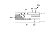
- FIG. 2 is a cross-sectional view (part 1) of a display device according to a comparative example.
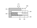
- FIG. 3 is a cross-sectional view (Part 2) of a display device according to a comparative example.
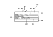
- FIG. 1 is a cross-sectional view of a display device according to a first embodiment of the present disclosure.
- FIG. 3 is a cross-sectional view (part 3) of a display device according to a comparative example.
- FIG. 4 is a cross-sectional view (No. 4) of a display device according to a comparative example.
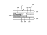
- FIG. 3 is a cross-sectional view of a display device according to a second embodiment of the present disclosure.
- FIG. 3 is a cross-sectional view (part 1) of a display device according to a third embodiment of the present disclosure.
- FIG. 3 is a cross-sectional view (part 2) of a display device according to a third embodiment of the present disclosure.
- FIG. 7 is a plan view (part 1) of a light shielding film according to a third embodiment of the present disclosure.
- FIG. 7 is a plan view (Part 2) of a light shielding film according to a third embodiment of the present disclosure.
- FIG. 7 is a cross-sectional view (part 1) of a light shielding film according to a fourth embodiment of the present disclosure.
- FIG. 7 is a cross-sectional view (part 2) of a light shielding film according to a fourth embodiment of the present disclosure.
- FIG. 7 is a cross-sectional view (part 3) of a light shielding film according to a fourth embodiment of the present disclosure.
- FIG. 4 is a cross-sectional view (part 4) of a light shielding film according to a fourth embodiment of the present disclosure.
- FIG. 5 is a cross-sectional view (part 5) of a light shielding film according to a fourth embodiment of the present disclosure.
- FIG. 7 is an explanatory diagram (Part 1) for explaining a method for manufacturing a display device according to a fifth embodiment of the present disclosure.
- FIG. 1 for explaining a method for manufacturing a display device according to a fifth embodiment of the present disclosure.
- FIG. 7 is an explanatory diagram (part 2) for explaining the method for manufacturing a display device according to the fifth embodiment of the present disclosure.
- FIG. 7 is an explanatory diagram (part 3) for explaining a method for manufacturing a display device according to a fifth embodiment of the present disclosure.
- FIG. 1 is a front view showing an example of the appearance of a digital still camera.
- FIG. 2 is a rear view showing an example of the appearance of a digital still camera. It is an external view of a head mounted display.
- FIG. 2 is an external view of a see-through head-mounted display. It is an external view of a television device. It is an external view of a smartphone.
- FIG. 1 is a diagram (part 1) showing the internal configuration of an automobile.
- FIG. 2 is a diagram (part 2) showing the internal configuration of the automobile.
- drawings referred to in the following description are drawings for explaining the embodiments of the present disclosure and promoting understanding thereof, and for the sake of clarity, the shapes, dimensions, ratios, etc. shown in the drawings are different from the actual ones. It may be different. Further, the display device shown in the drawings and the components included in the display device can be appropriately designed with reference to the following explanation and known techniques.
- the embodiment of the present disclosure will be described using an example where the embodiment of the present disclosure is applied to a display device that displays images, but the embodiment of the present disclosure is not applicable to such a display device.
- the present invention is not limited to this, and may be applied to a lighting device that irradiates light.
- FIG. 1 is a schematic plan view of a display device 100 according to an embodiment of the present disclosure and a display device 100a of a comparative example.
- 2 and 3 are cross-sectional views of a display device 100a according to a comparative example, and specifically correspond to a cross section when the display device 100a is cut along the line AA′ shown in FIG.
- FIGS. 1 to 3 are schematic plan views of a display device 100 according to an embodiment of the present disclosure and a display device 100a of a comparative example.
- the vertical direction of the stacked structure of the display device 100a corresponds to the relative direction when the display device 100a is arranged so that the light emitted by the display device 100a goes from the bottom to the top.
- the comparative example herein refers to the display device 100a that the present inventors had studied before creating the embodiment of the present disclosure.
- the display device 100a of the comparative example has a stacked structure (see FIG. 2) in which a BP (Back Plane) substrate 200 and a counter substrate 300 are stacked on each other.
- a display section 102 including a plurality of light emitting elements for example, LED (Light-Emitting Diode) elements
- a circuit section 104 including a drive circuit is provided around the display section 102 to drive the light emitting elements.
- a light emitting section 202 consisting of a plurality of light emitting elements (not shown), and a light emitting section 202 provided around the light emitting section 202 to drive the light emitting elements.
- a drive circuit section 204 including a drive circuit is provided.
- a color filter (CF) section 302 is provided, which is made of a material such as glass that transmits light and is composed of a plurality of color filters (not shown) that transmit light from light emitting elements. There is. Further, the CF section 302 is provided to face the light emitting section 202.
- the BP substrate 200 and the counter substrate 300 stacked on each other are sealed with a resin 452 located between the BP substrate 200 and the counter substrate 300. Further, the outer peripheral portion of the display device 100a is sealed with a seal member 450 made of resin.
- the drive circuit section 204 since the drive circuit section 204 is provided with wiring and electrodes made of a metal film, the metal film prevents the light from the light emitting element of the display device 100a and the light from the display device 100a. External light incident from the outside is reflected. Such reflected light causes the outer periphery of the image displayed on the display device 100a to appear white, thereby degrading the image quality and further reducing the immersive effect of the image.
- an outer frame 454 that does not transmit light is provided that surrounds the outer periphery of the display device 100a.
- an outer frame 454 by providing such an outer frame 454, reflection of light on the metal film of the drive circuit section 204 can be suppressed, and deterioration of image quality can be avoided.
- the inventors of the present invention have conducted extensive studies in order to suppress the increase in manufacturing costs while suppressing the reflection of light on the metal film of the drive circuit section 204. Then, the present inventors have created an embodiment of the present disclosure described below, which has a configuration of the display device 100 that intentionally does not include the outer frame 454 as described above. Details of such embodiments of the present disclosure will be sequentially described below.
- FIG. 4 is a cross-sectional view of the display device 100 according to the present embodiment, and specifically corresponds to a cross section when the display device 100 is cut along the line AA′ shown in FIG. Note that in FIG. 4, the vertical direction of the stacked structure of the display device 100 corresponds to the relative direction when the display device 100 is arranged so that the light emitted by the display device 100 goes from the bottom to the top.
- the display device 100 has a stacked structure in which a BP substrate (first substrate) 200 and a counter substrate (second substrate) 300 are stacked on each other.
- the BP substrate 200 includes a light emitting section (display section) 202 consisting of a plurality of light emitting elements (not shown), and a light emitting section (display section) 202 provided around the light emitting section 202 to drive the light emitting elements.
- a drive circuit section 204 including a drive circuit is provided for this purpose.
- the counter substrate 300 is provided with a CF section 302 made of a material such as glass that transmits the light from the light emitting elements, and consisting of a plurality of color filters (not shown) that transmit the light from the light emitting elements. There is.
- the CF section 302 is provided to face the light emitting section 202.
- the BP substrate 200 and the counter substrate 300 stacked on each other are sealed with a resin 452 made of, for example, a photocurable resin, located between the BP substrate 200 and the counter substrate 300. be done. Furthermore, the outer peripheral portion of the stacked structure of the display device 100 in plan view is sealed with a sealing member (photocurable resin) 450 made of, for example, a photocurable resin.
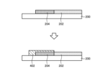
- a light shielding film (first light shielding film) 402 is provided that covers at least a portion of the drive circuit section 204 of the BP substrate 200. Furthermore, in this embodiment, at least part of the area of the surface of the counter substrate 300 facing the BP board 200 that does not face the light emitting part 202, in other words, at least part of the area facing the drive circuit part 204.
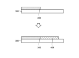
- a light-shielding film (second light-shielding film) 404 is provided to cover.
- a structure in which light shielding films 402 and 404 are provided on both the BP substrate 200 side and the counter substrate 300 side will be referred to as a light shielding structure.
- the light shielding film 402 on the BP substrate 200 side suppresses the reflection of light on the metal film of the drive circuit section 204 by covering the surface and side surfaces of the drive circuit section 204.
- the light shielding film 404 on the counter substrate 300 side covers the region of the counter substrate 300 that faces the drive circuit section 204, so that light from outside the display device 100 reaches the metal film of the drive circuit section 204. Suppresses reflection.
- the light shielding films 402 and 404 are provided such that the entire light shielding film 402 and the entire light shielding film 404 face each other. In other words, the light shielding films 402 and 404 are provided so that the entire light shielding film 402 and the entire light shielding film 404 overlap.
- the light shielding structure in which the light shielding films 402 and 404 are provided on both the BP substrate 200 side and the counter substrate 300 side more reliably suppresses the reflection of light on the metal film of the drive circuit section 204. Deterioration of image quality can be avoided. Furthermore, in this embodiment, since the outer frame 454 surrounding the outer periphery of the display device 100 is not provided, an increase in the manufacturing cost of the display device 100 can be suppressed.
- the light shielding structure shown in FIG. 4 may be provided along all four sides of the rectangular display device 100 shown in FIG. 1.
- this embodiment is not limited to providing the light shielding structure shown in FIG. 4 along all four sides of the display device 100.
- the light-shielding structure may be It may be provided on one side of the rectangular display device 100 or on a plurality of sides of 1 or more and 3 or less.
- the light shielding structure may be provided on the entirety of each side of the rectangular display device 100, or may be provided on a part of each side.
- the light shielding structure according to the present embodiment As described above, according to the light shielding structure according to the present embodiment, reflection of light on the metal film of the drive circuit section 204 can be suppressed more reliably. Furthermore, according to the present embodiment, since the above-mentioned outer frame 454 is intentionally not provided, an increase in the manufacturing cost of the display device 100 can be suppressed. Note that the detailed configuration of the light shielding films 402 and 404 according to this embodiment will be described later.
- FIGS. 5 and 6 are cross-sectional views of a display device 100a according to a comparative example
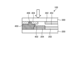
- FIG. 7 is a cross-sectional view of a display device 100 according to this embodiment.
- FIGS. 5 to 7 correspond to cross sections taken when the display devices 100 and 100a are cut along the line AA' shown in FIG. 1, and the light emitted by the display devices 100 and 100a is This corresponds to the relative direction when the display devices 100 and 100a are arranged so as to face upward.
- the comparative example here refers to the display device 100a that was studied by the present inventors before creating the embodiment of the present disclosure.
- the light shielding films 402 and 404 are provided on both the BP substrate 200 side and the counter substrate 300 side, thereby blocking light from the metal film of the drive circuit section 204. suppresses reflexes.
- FIG. 6 shows that from the viewpoint of suppressing the reflection of light at the drive circuit section 204, as shown in FIG. 6, even with a laminated structure in which a light shielding film 404 is provided on one side of the counter substrate 300, the reflection of light at the drive circuit section 204 can be prevented, although it is inferior to the first embodiment. It is possible to suppress it.
- the light shielding film 402 is provided only on the drive circuit section. It is provided so as to cover the entire surface and side surfaces of 204.
- the light shielding film 402 is formed from a material that has lower adhesion to the sealing member 450 than the surface of the drive circuit section 204 (for example, silicon oxide (SiO 2 ), etc.). Therefore, it is difficult to secure sealing of the display device 100a with the seal member 450 more reliably. Furthermore, if the sealing is insufficient, moisture may enter the inside of the display device 100a and peeling may occur.
- the contact area between the drive circuit section 204 and the sealing member 450 is required to be larger than a predetermined area. It is difficult to provide this so as to cover the entire surface and side surfaces of the drive circuit section 204.
- a contact area between the drive circuit section 204 and the sealing member 450 should be ensured to be at least a predetermined area. This is likely to become difficult.
- the light shielding film 404 is provided only on the opposite substrate 300 side. Of the surface facing the BP substrate 200 , it is provided so as to cover the entire area facing the drive circuit section 204 . In this case, although light reflection can be suppressed, the light shielding film 404 blocks light from outside the display device 100a, so the light does not reach the sealing member 450 and resin 452 inside the display device 100a during manufacturing. , the probability that these will not be sufficiently cured increases. Furthermore, if the curing is insufficient, moisture may enter the inside of the display device 100a and peeling may occur.
- the contact area between the drive circuit section 204 and the sealing member 450 is reduced to a predetermined area while more reliably suppressing the reflection of light on the metal film of the drive circuit section 204.
- a light-shielding structure that can ensure the above-mentioned properties and also sufficiently photocure the sealing member 450 and the resin 452.
- the light shielding film 402 provided on the BP substrate 200 side is provided so as to cover only a part of the drive circuit section 204
- the light shielding film 402 provided on the counter substrate 300 side is provided so as to cover only a part of the drive circuit section 204.
- the light shielding film 404 is provided so as to cover only a part of the region of the counter substrate 300 that faces the drive circuit section 204 .
- the sealing member 450 and the surface of the drive circuit section 204 are directly connected to each other. can be contacted.
- the light shielding films 402 and 404 are not provided so that the entire light shielding film 402 and the entire light shielding film 404 completely overlap. More specifically, in the example shown in FIG. 7, in the light shielding films 402 and 404, a part of the light shielding film 402 and a part of the light shielding film 404 face each other (overlapping each other), and the remaining part of the light shielding film 402 and the light shielding film 404 are provided so that they do not face (do not overlap) the rest of the board. Note that in this embodiment, the shape is not limited to that shown in FIG. They may be provided alternately. That is, in this embodiment, the light shielding films 402 and 404 may be provided so that the entire light shielding film 402 and the entire light shielding film 404 do not completely overlap.
- the light shielding film 404 provided on the counter substrate 300 side is provided so as to cover only a part of the region of the counter substrate 300 that faces the drive circuit section 204. Therefore, in this embodiment, the light from the outside of the display device 100 is not completely blocked by the light shielding film 404, so that light does not reach the sealing member 450 and resin 452 inside the display device 100 during manufacturing. becomes. As a result, according to the present embodiment, the sealing member 450 and resin 452 inside the display device 100 can be sufficiently cured, so that moisture enters the inside of the display device 100 and peeling etc. occur. can be avoided.
- the drive circuit Reflection of light on the metal film of the portion 204 can be suppressed.
- the light shielding film 402 provided on the BP substrate 200 side covers only a part of the drive circuit section 204 and does not cover the entire drive circuit section 204, so that the sealing member 450 and the drive circuit section 204 are The surface of the circuit section 204 can be directly contacted. Therefore, in this embodiment, it is easy to make the contact area between the drive circuit section 204 and the seal member 450 larger than a predetermined width. In addition, even if the frame becomes narrower, according to this embodiment, it is easy to ensure that the contact area between the drive circuit section 204 and the seal member 450 is equal to or larger than a predetermined width.
- the contact area between the drive circuit section 204 and the seal member 450 it is possible to make the contact area between the drive circuit section 204 and the seal member 450 larger than a predetermined width, and to ensure the close contact between the light shielding film 402 and the seal member 450.
- sealing of the display device 100 by the sealing member 450 can be ensured more reliably, so it is possible to avoid moisture from entering the inside of the display device 100 and occurrence of peeling, etc. .
- FIGS. 8 to 11 are cross-sectional views of the display device 100 according to the present embodiment, and in detail, they correspond to the cross sections when the display device 100 is cut along the line AA' shown in FIG. .
- the vertical direction of the stacked structure of the display device 100 corresponds to the relative direction when the display device 100 is arranged so that the light emitted by the display device 100 goes from the bottom to the top.
- FIGS. 10 and 11 are plan views of the light shielding film 404 according to this embodiment.
- the light shielding film 404 provided on the counter substrate 300 side is provided so as to cover only a part of the region of the counter substrate 300 that faces the drive circuit section 204.
- the light from the outside of the display device 100 is not completely blocked by the light shielding film 404, so that the sealing member inside the display device 100 is removed during manufacturing.
- the light reaches the resin 450 and the resin 452. Therefore, in the third embodiment of the present disclosure, similarly to the second embodiment, an opening is formed in the light shielding film 404 in order to allow light to reach the sealing member 450 and resin 452 inside the display device 100 during manufacturing. will be established.
- a light shielding film 404 provided on the counter substrate 300 side is provided with a sealing member 450 inside the display device 100 and a resin film to prevent light from outside the display device 100.
- An opening (opening) 406 is provided for leading to 452 . Therefore, in this embodiment, since the opening 406 can efficiently guide light from outside the display device 100 to the sealing member 450 and resin 452 inside the display device 100, the display device 100 is The light reaches the sealing member 450 and the resin 452 inside the device more reliably. As a result, according to the present embodiment, the sealing member 450 and the resin 452 inside the display device 100 are easily cured sufficiently, so that moisture enters the inside of the display device 100 and peeling occurs. This can be avoided more easily.
- the number of openings 406 provided in the light shielding film 404 is not limited to one, and may be plural.
- the light shielding film 404 may have one or more rectangular slits, or may have a lattice or checkerboard shape. You may also Further, in the present embodiment, the shape of the opening 406 is not limited to a rectangular shape, and may be, for example, a circular shape, an elliptical shape, a polygonal shape, or the like.
- the light shielding film 404 may have a lattice shape as shown in FIG. 10 or may have a checkered pattern as shown in FIG. 11.
- the area of the opening 406 of the light shielding film 404 in plan view is smaller than the area of the entire light shielding film 404 in plan view. It is preferable that the area is 25% or more of the area (area of the light shielding film 404 including the opening 406).
- the present inventors created a light-shielding film 404 in which the area of the opening 406 was varied, and irradiated UV (Ultra Violet) light from the outside of the display device 100 to seal the inside of the display device 100. It was confirmed whether the member 450 and the resin 452 were sufficiently cured.
- the sealing member 450 and resin 452 inside the display device 100 were sufficiently cured when the area of the opening 406 was set to 25% and 50%. Therefore, in this embodiment, the area of the opening 406 of the light shielding film 404 in plan view is preferably 25% or more of the entire area of the light shielding film 404 in plan view.
- the light shielding films 402 and 404 are provided, for example, at least alternately in the stacking direction so as to suppress reflection of light on the metal film of the drive circuit section 204.
- the light shielding film 402 on the BP substrate 200 side may also have an opening 406.
- the light shielding films 402 and 404 can be 402 may also have one or more slits, or may have a grid or checkerboard shape.
- the sealing member 450 and the resin 452 inside the display device 100 are easily cured sufficiently, so that moisture enters the inside of the display device 100 and peeling occurs. This can be avoided more easily.
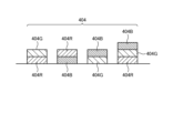
- FIGS. 12 to 16 are cross-sectional views of the light shielding film 404 according to the present embodiment, and specifically correspond to the cross-section when the display device 100 is cut along the line AA' shown in FIG. .
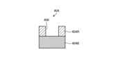
- 14 and 15 are cross-sectional views of the light-shielding film 404 according to the present embodiment, and specifically correspond to the cross-sections when the light-shielding film 404 is cut along the line BB′ shown in FIG. .
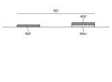
- FIG. 16 is a cross-sectional view of the light shielding film 402 according to the present embodiment, and specifically corresponds to a cross section when the display device 100 is cut along the line AA′ shown in FIG.
- the light shielding films 402 and 404 can be formed from any material that can shield light, such as an organic material film or an inorganic material film, and are not particularly limited. Further, in this embodiment, the light shielding films 402 and 404 may be a single layer film or a laminated film consisting of a plurality of layers, as long as they can block light, and are not particularly limited. isn't it. Furthermore, in this embodiment, when the light shielding films 402 and 404 are laminated films, they may be a lamination of different organic material films, a lamination of different inorganic material films, or a lamination of an organic material film and an inorganic material film. may be used, and is not particularly limited.
- the light shielding film 404 provided on the counter substrate 300 side is provided on the surface of the counter substrate 300 that faces the BP substrate 200.
- the light shielding film 404 can be formed from a color resist, for example, a green color resist (green resist) 404G, a red color resist (red resist) 404R. , a blue color resist (blue resist) 404B, a black color resist (black resist) 404L, and the like.
- a color resist made of the same material as the color filter provided on the CF section 302 of the counter substrate 300 as the light shielding film 404 provided on the counter substrate 300, the number of manufacturing steps of the display device 100 can be reduced. It is possible to effectively block light from the outside of the display device 100 while avoiding the above.
- the light shielding film 404 may be a laminated film in which different color resists are laminated.
- the light shielding film 404 may be a laminated film in which a green color resist 404G is laminated on a red color resist 404R, as shown on the left side of FIG. , a laminated film in which a red color resist 404R is laminated on a blue color resist 404B.
- the light shielding film 404 may be a laminated film in which a blue color resist 404B is laminated on a green color resist 404G, as shown third from the left in FIG.
- It may be a laminated film in which a green color resist 404G and a blue color resist 404B are sequentially laminated on a red color resist 404R.
- the light shielding of the light shielding film 404 can be improved. The effect can be increased. That is, in this embodiment, the type of color resist, the combination thereof, and the number of laminated layers of the light-shielding film 404 can be selected as appropriate depending on the purpose and the like.
- the light shielding film 404 has an opening 406 on a color resist having no opening 406 (blue color resist 404B in FIG. 14). It may also be a laminated film in which color resists (in FIG. 14, red color resist 404R) are laminated.
- the light shielding film 404 has a narrow opening so as to cover a color resist having a wide opening 406 (red color resist 404R in FIG. 15).
- a form in which a color resist (blue color resist 404B in FIG. 15) having a portion 406 is formed may be used.
- the light shielding film 402 on the BP substrate 200 side may also be formed from a color resist, or may be a laminated film in which different color resists are laminated.
- the light shielding film 402 provided on the BP substrate 200 side is provided on the surface of the BP substrate 200 that faces the counter substrate 300 .
- the light shielding film 402 can be formed of a low-reflection metal film 402f or the like with low reflectance.
- the low-reflection metal film 402f include titanium nitride (TiN), titanium oxynitride (TiON), chromium (Cr), chromium oxide (CrO 2 ), and tungsten silicide (WSi).
- the formation of the light shielding film 402 made of such a low reflection metal film 402f can be performed following the step of forming the drive circuit section 204 provided on the BP substrate 200. Therefore, according to the present embodiment, it is possible to effectively block light from outside the display device 100 while avoiding a significant increase in the manufacturing process of the display device 100.
- the light shielding film 402 may be a laminated film in which a low reflection metal film 402f and a metal film 402m are laminated.
- the metal film 402m can be made of, for example, titanium, aluminum (Al), or the like.
- the light-shielding film 402 may be only the low-reflection metal film 402f, or may be a laminated film in which the low-reflection metal film 402f and the metal film 402m are laminated, depending on the application. .
- the light shielding film 404 on the counter substrate 300 side may also be a low-reflection metal film 402f, or a laminated film in which a low-reflection metal film 402f and a metal film 402m are laminated. good.
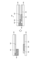
- FIGS. 17A to 17C are explanatory diagrams for explaining the manufacturing method of the display device 100 according to this embodiment, and specifically correspond to the cross-sectional view shown in FIG. 4.
- a light emitting section 202 consisting of a plurality of light emitting elements (not shown) and a drive circuit section 204 including a drive circuit for driving the light emitting elements are formed around the light emitting section 202 on the BP substrate 200, and as shown in FIG. The form shown in the upper row of can be obtained. Further, a light shielding film 402 is formed to cover the drive circuit section 204 of the BP substrate 200, thereby obtaining a configuration as shown in the lower part of FIG. 17A.
- a CF section 302 consisting of a plurality of color filters (not shown) that transmits light from light emitting elements is formed on the counter substrate 300, and a configuration as shown in the upper part of FIG. 17B can be obtained.
- a light shielding film 404 is formed so as to cover the area facing the drive circuit section 204 on the surface of the counter substrate 300 facing the BP substrate 200, thereby obtaining a form as shown in the lower part of FIG. 17B. I can do it.
- a sealing member 450 made of, for example, a photocurable resin is formed on the outer peripheral portion of the counter substrate 300 in plan view. Then, the BP substrate 200 and the counter substrate 300 thus formed are stacked, facing each other with the resin 452 (not shown in FIG. 17C) interposed therebetween, as shown on the left side of FIG. 17C. Then, by irradiating UV light from the outside and curing the sealing member 450 and the resin 452, the display device 100 can be formed as shown on the right side of FIG. 17C.
- the display device 100 according to the embodiment of the present disclosure can be manufactured using methods, devices, and conditions used for manufacturing general semiconductor devices and electronic devices.
- Each substrate of the display device 100 according to this embodiment can be manufactured using, for example, an existing semiconductor device manufacturing method.
- examples of the above-mentioned methods include the PVD (Physical Vapor Deposition) method, the CVD (Chemical Vapor Deposition) method, and the ALD (Atomic Layer Deposition) method.
- PVD Physical Vapor Deposition
- CVD Chemical Vapor Deposition
- ALD Atomic Layer Deposition
- Examples of the PVD method include vacuum evaporation, EB (electron beam) evaporation, various sputtering methods (magnetron sputtering, RF (Radio Frequency)-DC (Direct Current) coupled bias sputtering, and ECR (Electron Cyclotron Resonance).
- examples of the CVD method include a plasma CVD method, a thermal CVD method, an organic metal (MO) CVD method, and a photoCVD method.
- other methods include electrolytic plating, electroless plating, spin coating, dipping, casting, micro contact printing, drop casting, screen printing, inkjet printing, offset printing, and gravure printing.
- various printing methods such as flexographic printing method; stamp method; spray method; air doctor coater method, blade coater method, rod coater method, knife coater method, squeeze coater method, reverse roll coater method, transfer roll coater method, gravure coater method , a kiss coater method, a cast coater method, a spray coater method, a slit orifice coater method, and a calendar coater method.
- the patterning method include chemical etching such as shadow masking, laser transfer, and photolithography, and physical etching using ultraviolet rays, laser, and the like.
- examples of the planarization technique include a CMP (Chemical Mechanical Polishing) method, a laser planarization method, a reflow method, and the like.
- the display device 100 can be manufactured because the outer frame 454 is intentionally not provided while the reflection of light on the metal film of the drive circuit section 204 is more reliably suppressed. Cost increases can be suppressed.
- the technology of the present disclosure is not only applied to the display device 100 but may also be applied to a lighting device or the like. Furthermore, the technology of the present disclosure can also be applied to an imaging device having a plurality of imaging elements.
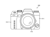
- FIG. 18A is a front view showing an example of the external appearance of the digital still camera 500
- FIG. 18B is a rear view showing an example of the external appearance of the digital still camera 500.
- This digital still camera 500 is a single-lens reflex type with interchangeable lenses, and has an interchangeable photographic lens unit (interchangeable lens) 512 approximately in the center of the front of a camera body 511, and on the left side of the front. It has a grip part 513 for the photographer to hold.
- interchangeable photographic lens unit interchangeable lens
- a monitor 514 is provided at a position shifted to the left from the center of the back surface of the camera body section 511.
- an electronic viewfinder (eyepiece window) 515 is provided at the top of the monitor 514.
- the display device 100 can be used. Even if the digital still camera 500 is small, the image display surface can be made wider by applying the display device 100 according to the embodiment of the present disclosure.
- FIG. 19 is an external view of the head mounted display 600.
- the head-mounted display 600 has, for example, ear hooks 612 on both sides of a glasses-shaped display section 611 to be worn on the user's head.
- the display device 100 according to the embodiment of the present disclosure can be used as the display section 611.
- the image display surface of the head-mounted display 600 can be made wider.
- FIG. 20 is an external view of the see-through head-mounted display 634.
- the see-through head-mounted display 634 includes a main body 632, an arm 633, and a lens barrel 631.
- the main body portion 632 is connected to the arm 643 and the glasses 630. Specifically, an end of the main body 632 in the long side direction is coupled to an arm 633, and one side of the main body 632 is coupled to the glasses 630 via a connecting member. Note that the main body portion 632 may be directly attached to the human head.
- the main body section 632 incorporates a control board for controlling the operation of the see-through head-mounted display 634 and a display section.
- the arm 633 connects the main body 632 and the lens barrel 631 and supports the lens barrel 631. Specifically, the arm 633 is coupled to an end of the main body 632 and an end of the lens barrel 631, respectively, and fixes the lens barrel 631. Further, the arm 633 has a built-in signal line for communicating data related to an image provided from the main body 632 to the lens barrel 631.
- the lens barrel 631 projects image light provided from the main body 632 via the arm 633 toward the eyes of the user wearing the see-through head-mounted display 634 through the eyepiece.
- the display device 100 according to the embodiment of the present disclosure can be used for the display section of the main body section 632.
- FIG. 21 shows an example of the appearance of the television device 710.
- This television device 710 has, for example, a video display screen section 711 including a front panel 712 and a filter glass 713, and this video display screen section 711 is configured by the display device 100 according to the embodiment of the present disclosure. .
- the display device 100 according to the embodiment of the present disclosure to the television device 710, it is possible to make the image display surface wider while avoiding deterioration in image quality.
- the display device 100 according to the embodiment of the present disclosure to the television device 710, there is no need to provide the outer frame 454, so an increase in the manufacturing cost of the television device 710 can be suppressed.
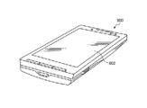
- FIG. 22 shows an example of the appearance of the smartphone 800.
- the smartphone 800 includes a display section 802 that displays various information, and an operation section that includes buttons that accept operation inputs from the user.
- the display unit 802 can be the display device 100 according to the present embodiment. By applying the display device 100 according to the embodiment of the present disclosure, the image display surface of the smartphone 800 can be made wider.
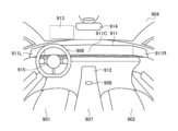
- FIGS. 23A and 23B are diagrams showing the internal configuration of an automobile that has the display device 100 according to the embodiment of the present disclosure as a display device. Specifically, FIG. 23A is a diagram showing the interior of the vehicle from the rear to the front, and FIG. 23B is a diagram showing the interior of the vehicle from the diagonal rear to the diagonal front.
- the automobile shown in FIGS. 23A and 23B has a center display 911, a console display 912, a head-up display 913, a digital rear mirror 914, a steering wheel display 915, and a rear entertainment display 916.
- the display device 100 according to the embodiment of the present disclosure can be applied to some or all of these displays. By applying the display device 100 according to the embodiment of the present disclosure, the image display surfaces of the center display 911, console display 912, head-up display 913, digital rear mirror 914, steering wheel display 915, and rear entertainment display 916 can be improved. Can be made wider.
- the center display 911 is arranged on the center console 907 at a location facing the driver's seat 901 and the passenger seat 902.
- 23A and 23B show an example of a horizontally long center display 911 extending from the driver's seat 901 side to the passenger seat 902 side, but the screen size and placement location of the center display 911 are arbitrary.
- the center display 911 can display information detected by various sensors (not shown). As a specific example, the center display 911 displays images taken by an image sensor, distance images to obstacles in front of and on the sides of the vehicle measured by a ToF (Time of Flight) sensor, and images detected by an infrared sensor. It is possible to display information such as the passenger's body temperature.
- the center display 911 can be used, for example, to display at least one of safety-related information, operation-related information, life log, health-related information, authentication/identification-related information, and entertainment-related information.
- Safety-related information includes information such as detection of falling asleep, detection of looking away, detection of mischief by children in the same vehicle, presence or absence of seatbelts, and detection of leaving passengers behind.
- the sensor (not shown).
- the operation-related information uses sensors to detect gestures related to operations by the occupant.
- the detected gestures may include operations on various equipment within the vehicle. For example, the operation of air conditioning equipment, navigation equipment, AV (Audio/Visual) equipment, lighting equipment, etc. is detected.
- the life log includes life logs of all crew members.
- a life log includes a record of the actions of each occupant during the ride.
- a temperature sensor is used to detect the occupant's body temperature, and the occupant's health condition is estimated based on the detected body temperature.
- an image sensor may be used to capture an image of the occupant's face, and the occupant's health condition may be estimated from the captured facial expression.
- Authentication/identification related information includes a keyless entry function that performs facial recognition using a sensor, and a function that automatically adjusts seat height and position using facial recognition.
- the entertainment-related information includes a function that uses a sensor to detect operation information of an AV device by a passenger, a function that recognizes the passenger's face using a sensor, and provides the AV device with content suitable for the passenger.
- the console display 912 can be used, for example, to display life log information.
- the console display 912 is arranged near the shift lever 908 on the center console 907 between the driver's seat 901 and the passenger seat 902.
- the console display 912 can also display information detected by various sensors (not shown). Further, the console display 912 may display an image around the vehicle captured by an image sensor, or may display a distance image to an obstacle around the vehicle.
- a head-up display 913 is virtually displayed behind the windshield 904 in front of the driver's seat 901.
- the head-up display 913 can be used, for example, to display at least one of safety-related information, operation-related information, life log, health-related information, authentication/identification-related information, and entertainment-related information. Since the head-up display 913 is often placed virtually in front of the driver's seat 901, it is suitable for displaying information directly related to the operation of the vehicle, such as the speed of the vehicle and the remaining amount of fuel (battery). There is.
- the display device 100 according to the embodiment of the present disclosure to the head-up display 913, there is no need to provide the outer frame 454, so it is possible to avoid obstructing the driver's view of the front of the vehicle.
- the digital rear mirror 914 can display not only the rear of the car but also the state of the occupants in the rear seats. Therefore, by placing a sensor (not shown) on the back side of the digital rear mirror 914, for example, life log information can be displayed. Can be used for display.
- the steering wheel display 915 is placed near the center of the steering wheel 906 of the automobile.
- Steering wheel display 915 can be used, for example, to display at least one of safety-related information, operation-related information, life log, health-related information, authentication/identification-related information, and entertainment-related information.
- life log information such as the driver's body temperature, and information regarding the operation of AV equipment, air conditioning equipment, etc. There is.
- the rear entertainment display 916 is attached to the back side of the driver's seat 901 and the passenger seat 902, and is for viewing by passengers in the rear seats.
- Rear entertainment display 916 can be used, for example, to display at least one of safety-related information, operation-related information, lifelog, health-related information, authentication/identification-related information, and entertainment-related information.
- information relevant to the rear seat occupant is displayed. For example, information regarding the operation of the AV device or air conditioning equipment may be displayed, or the results of measuring the body temperature of the occupant in the rear seat using a temperature sensor (not shown) may be displayed.
- a first substrate having a display section including a plurality of light emitting elements and a drive circuit section provided around the display section, and a second substrate that transmits light from the plurality of light emitting elements are laminated together.
- a display device comprising: (2) The display according to (1) above, wherein the first and second light-shielding films are provided such that at least a portion of the first light-shielding film and at least a portion of the second light-shielding film face each other. Device. (3) The display device according to (2), wherein the first and second light-shielding films are provided such that the entire first light-shielding film and the second light-shielding film overlap. (4) The display device according to (1) above, wherein the first and second light shielding films are provided so that the first light shielding film and the second light shielding film do not overlap.
- the display device according to any one of (1) to (4) above, wherein the first and second light shielding films have one or more openings.
- the first and second light-shielding films have a grid-like or checkerboard-like shape.
- the area of the opening provided in the second light shielding film in plan view is 25% or more of the area of the second light shielding film in plan view. .
- the display device according to any one of (1) to (7) above, wherein at least one of the first and second light-shielding films is made of an organic material film.
- the low-reflection metal film is at least one selected from the group consisting of titanium nitride, titanium oxynitride, chromium, chromium oxide, and tungsten silicide.
- the display device includes: A first substrate having a display section including a plurality of light emitting elements and a drive circuit section provided around the display section, and a second substrate that transmits light from the plurality of light emitting elements are laminated together.
- a light-shielding structure consisting of a light-shielding film; has, Electronics.
Landscapes
- Physics & Mathematics (AREA)
- General Physics & Mathematics (AREA)
- Optics & Photonics (AREA)
- Engineering & Computer Science (AREA)
- Theoretical Computer Science (AREA)
- Devices For Indicating Variable Information By Combining Individual Elements (AREA)
- Electroluminescent Light Sources (AREA)
Abstract
Description
1. 本発明者らが本開示の実施形態を創作するに至った背景
2. 第1の実施形態
3. 第2の実施形態
4. 第3の実施形態
5. 第4の実施形態
6. 第5の実施形態
7. まとめ
8. 応用例
9. 補足
まず、本開示の実施形態の詳細を説明する前に、本発明者らが本開示の実施形態を創作するに至った背景について、図1から図3を参照して説明する。図1は、本開示の実施形態に係る表示装置100及び比較例の表示装置100aの平面模式図である。図2及び図3は、比較例に係る表示装置100aの断面図であり、詳細には、図1に示すA-A´線に沿って表示装置100aを切断した場合の断面に対応する。また、図2及び図3においては、表示装置100aの積層構造の上下方向は、表示装置100aが放射する光が下から上へ向かうように、表示装置100aを配置した場合の相対方向に対応する。なお、ここで比較例とは、本発明者らが、本開示の実施形態を創作する前に、検討を行っていた表示装置100aを意味するものとする。
まずは、図4を参照して、本開示の第1の実施形態に係る表示装置100を説明する。図4は、本実施形態に係る表示装置100の断面図であって、詳細には、図1に示すA-A´線に沿って表示装置100を切断した場合の断面に対応する。なお、図4においては、表示装置100の積層構造の上下方向は、表示装置100が放射する光が下から上へ向かうように、表示装置100を配置した場合の相対方向に対応する。
次に、図5から図7を参照して、本開示の第2の実施形態を説明する。図5及び図6は、比較例に係る表示装置100aの断面図であり、図7は、本実施形態に係る表示装置100の断面図である。詳細には、図5から図7は、図1に示すA-A´線に沿って表示装置100、100aを切断した場合の断面に対応し、表示装置100、100aが放射する光が下から上へ向かうように、表示装置100、100aを配置した場合の相対方向に対応する。なお、ここで比較例とは、先に説明したように、本発明者らが、本開示の実施形態を創作する前に、検討を行っていた表示装置100aを意味するものとする。
次に、図8から図11を参照して、本開示の第3の実施形態に係る表示装置100を説明する。図8及び図9は、本実施形態に係る表示装置100の断面図であって、詳細には、図1に示すA-A´線に沿って表示装置100を切断した場合の断面に対応する。なお、図8及び図9においては、表示装置100の積層構造の上下方向は、表示装置100が放射する光が下から上へ向かうように、表示装置100を配置した場合の相対方向に対応する。また、図10及び図11は、本実施形態に係る遮光膜404の平面図である。
次に、図12から図16を参照して、本開示の第4の実施形態に係る遮光膜402、404を説明する。図12及び図13は、本実施形態に係る遮光膜404の断面図であって、詳細には、図1に示すA-A´線に沿って表示装置100を切断した場合の断面に対応する。図14及び図15は、本実施形態に係る遮光膜404の断面図であって、詳細には、図10に示すB-B´線に沿って遮光膜404を切断した場合の断面に対応する。また、図16は、本実施形態に係る遮光膜402の断面図であって、詳細には、図1に示すA-A´線に沿って表示装置100を切断した場合の断面に対応する。
次に、本実施形態に係る表示装置100の製造工程(製造方法)の一部について、図17Aから図17Cを参照して説明する。図17Aから図17Cは、本実施形態に係る表示装置100の製造方法を説明するための説明図であり、詳細には、図4に示す断面図に対応する。
以上のように、本開示の各実施形態によれば、駆動回路部204の金属膜での光の反射をより確実に抑制しつつ、外枠454をあえて設けないことから、表示装置100の製造コストの増加を抑えることができる。
例えば、本開示に係る技術は、様々な電子機器の表示部等に適用されてもよい。そこで、以下、本技術を適用することができる電子機器の例について説明する。
図18Aは、デジタルスチルカメラ500の外観の一例を示す正面図であり、図18Bは、デジタルスチルカメラ500の外観の一例を示す背面図である。このデジタルスチルカメラ500は、レンズ交換式一眼レフレックスタイプのものであり、カメラ本体部(カメラボディ)511の正面略中央に交換式の撮影レンズユニット(交換レンズ)512を有し、正面左側に撮影者が把持するためのグリップ部513を有している。
図19は、ヘッドマウントディスプレイ600の外観図である。ヘッドマウントディスプレイ600は、例えば、眼鏡形の表示部611の両側に、使用者の頭部に装着するための耳掛け部612を有している。このヘッドマウントディスプレイ600において、その表示部611として本開示の実施形態に係る表示装置100を用いることができる。本開示の実施形態に係る表示装置100を適用することにより、ヘッドマウントディスプレイ600の画像表示面をより広くすることができる。
図20は、シースルーヘッドマウントディスプレイ634の外観図である。シースルーヘッドマウントディスプレイ634は、本体部632、アーム633および鏡筒631で構成される。
図21は、テレビジョン装置710の外観の一例を示す。このテレビジョン装置710は、例えば、フロントパネル712およびフィルターガラス713を含む映像表示画面部711を有し、この映像表示画面部711は、本開示の実施形態に係る表示装置100により構成されている。本開示の実施形態に係る表示装置100をテレビジョン装置710に適用することにより、画質の劣化を避けつつ、画像表示面をより広くすることができる。さらに、本開示の実施形態に係る表示装置100をテレビジョン装置710に適用することにより、外枠454を設ける必要がないことから、テレビジョン装置710の製造コストの増加を抑えることができる。
図22は、スマートフォン800の外観の一例を示す。スマートフォン800は、各種情報を表示する表示部802や、ユーザによる操作入力を受け付けるボタン等から構成される操作部等を有する。上記表示部802は、本実施形態に係る表示装置100であることができる。本開示の実施形態に係る表示装置100を適用することにより、スマートフォン800の画像表示面をより広くすることができる。
図23A及び図23Bは本開示の実施形態に係る表示装置100を表示装置として有する自動車の内部の構成を示す図である。詳細には、図23Aは自動車の後方から前方にかけての自動車の内部の様子を示す図であり、図23Bは自動車の斜め後方から斜め前方にかけての自動車の内部の様子を示す図である。
以上、添付図面を参照しながら本開示の好適な実施形態について詳細に説明したが、本開示の技術的範囲はかかる例に限定されない。本開示の技術分野における通常の知識を有する者であれば、請求の範囲に記載された技術的思想の範疇内において、各種の変更例または修正例に想到し得ることは明らかであり、これらについても、当然に本開示の技術的範囲に属するものと了解される。
(1)
複数の発光素子からなる表示部、及び、当該表示部の周囲に設けられた駆動回路部を有する第1の基板と、前記複数の発光素子からの光を透過する第2の基板とが互いに積層された積層構造と、
前記駆動回路部の少なくとも一部を覆う第1の遮光膜と、前記第2の基板の前記第1の基板と対向する面のうち前記駆動回路部と対向する領域の少なくとも一部を覆う第2の遮光膜とからなる遮光構造と、
を備える、表示装置。
(2)
前記第1及び第2の遮光膜は、前記第1の遮光膜の少なくとも一部と、前記第2の遮光膜の少なくとも一部とが対向するように設けられる、上記(1)に記載の表示装置。
(3)
前記第1及び第2の遮光膜は、前記第1の遮光膜の全体と前記第2の遮光膜の全体とが重なりあうように設けられる、上記(2)に記載の表示装置。
(4)
前記第1及び第2の遮光膜は、前記第1の遮光膜と前記第2の遮光膜とが重なり合わないように設けられる、上記(1)に記載の表示装置。
(5)
前記第1及び第2の遮光膜は、1つ以上の開口を持つ、上記(1)~(4)のいずれか1つに記載の表示装置。
(6)
前記第1及び第2の遮光膜は、格子状、又は、市松模様状の形状を持つ、上記(5)に記載の表示装置。
(7)
前記第2の遮光膜に設けられた前記開口の平面視における面積は、前記第2の遮光膜の平面視における面積に対する25%以上である、上記(5)又は(6)に記載の表示装置。
(8)
前記第1及び第2の遮光膜のうちの少なくとも一方は、有機材料膜からなる、上記(1)~(7)のいずれか1つに記載の表示装置。
(9)
前記第1及び第2の遮光膜のうちの少なくとも一方は、カラーレジストからなる、上記(8)に記載の表示装置。
(10)
前記第1及び第2の遮光膜のうちの少なくとも一方は、積層された複数の前記カラーレジストからなる、上記(9)に記載の表示装置。
(11)
前記カラーレジストは、赤色レジスト、緑色レジスト、青色レジスト、及び、黒色レジストからなる群から選択される少なくとも1つからなる、上記(9)又は(10)に記載の表示装置。
(12)
前記第1及び第2の遮光膜のうちの少なくとも一方は、無機材料膜からなる、上記(1)~(7)のいずれか1つに記載の表示装置。
(13)
前記第1及び第2の遮光膜のうちの少なくとも一方は、低反射金属膜を含む、上記(12)に記載の表示装置。
(14)
前記第1及び第2の遮光膜のうちの少なくとも一方は、積層された前記低反射金属膜と金属膜とからなる、上記(13)に記載の表示装置。
(15)
前記低反射金属膜は、窒化チタン、酸窒化チタン、クロム、酸化クロム、及び、タングステンシリサイドからなる群から選択される少なくとも1つである、上記(13)又は(14)に記載の表示装置。
(16)
前記積層構造の平面視における外周において、前記第1の基板と前記第2の基板との間を封止する、光硬化性樹脂からなるシール部材をさらに備える、上記(1)~(15)のいずれか1つに記載の表示装置。
(17)
前記シール部材は、前記駆動回路部の表面と直接接触するように設けられる、上記(16)に記載の表示装置。
(18)
前記第1の基板と前記第2の基板との間を封止する、光硬化性樹脂からなる樹脂をさらに備える、上記(1)~(17)のいずれか1つに記載の表示装置。
(19)
前記積層構造は、平面視において、矩形状の形状を持ち、
前記遮光構造は、前記積層構造の平面視における4辺のうちの少なくとも1辺のうちの少なくとも一部に沿って設けられる、
上記(1)~(18)のいずれか1つに記載の表示装置。
(20)
表示装置を搭載した電子機器であって、
前記表示装置は、
複数の発光素子からなる表示部、及び、当該表示部の周囲に設けられた駆動回路部を有する第1の基板と、前記複数の発光素子からの光を透過する第2の基板とが互いに積層された積層構造と、
前記駆動回路部の少なくとも一部を覆う第1の遮光膜と、前記第2の基板の前記第1の基板と対向する面のうち前記駆動回路部と対向する領域の少なくとも一部を覆う第2の遮光膜とからなる遮光構造と、
を有する、
電子機器。
102、611、802 表示部
104 回路部
200 BP基板
202 発光部
204 駆動回路部
300 対向基板
302 CF部
402、404 遮光膜
402f 低反射金属膜
402m 金属膜
404B、404G、404L、404R カラーレジスト
406 開口部
450 シール部材
452 樹脂
454 外枠
500 デジタルスチルカメラ
511 カメラ本体部
512 撮影レンズユニット
513 グリップ部
514 モニタ
515 電子ビューファインダ
600 ヘッドマウントディスプレイ
612 耳掛け部
630 眼鏡
631 鏡筒
632 本体部
633、643 アーム
634 シースルーヘッドマウントディスプレイ
710 テレビジョン装置
711 映像表示画面部
712 フロントパネル
713 フィルターガラス
800 スマートフォン
901 運転席
902 助手席
904 フロントガラス
906 ハンドル
907 センターコンソール
908 シフトレバー
911 センターディスプレイ
912 コンソールディスプレイ
913 ヘッドアップディスプレイ
914 デジタルリアミラー
915 ステアリングホイールディスプレイ
916 リアエンタテイメントディスプレイ
Claims (20)
- 複数の発光素子からなる表示部、及び、当該表示部の周囲に設けられた駆動回路部を有する第1の基板と、前記複数の発光素子からの光を透過する第2の基板とが互いに積層された積層構造と、
前記駆動回路部の少なくとも一部を覆う第1の遮光膜と、前記第2の基板の前記第1の基板と対向する面のうち前記駆動回路部と対向する領域の少なくとも一部を覆う第2の遮光膜とからなる遮光構造と、
を備える、表示装置。 - 前記第1及び第2の遮光膜は、前記第1の遮光膜の少なくとも一部と、前記第2の遮光膜の少なくとも一部とが対向するように設けられる、請求項1に記載の表示装置。
- 前記第1及び第2の遮光膜は、前記第1の遮光膜の全体と前記第2の遮光膜の全体とが重なりあうように設けられる、請求項2に記載の表示装置。
- 前記第1及び第2の遮光膜は、前記第1の遮光膜と前記第2の遮光膜とが重なり合わないように設けられる、請求項1に記載の表示装置。
- 前記第1及び第2の遮光膜は、1つ以上の開口を持つ、請求項1に記載の表示装置。
- 前記第1及び第2の遮光膜は、格子状、又は、市松模様状の形状を持つ、請求項5に記載の表示装置。
- 前記第2の遮光膜に設けられた前記開口の平面視における面積は、前記第2の遮光膜の平面視における面積に対する25%以上である、請求項5に記載の表示装置。
- 前記第1及び第2の遮光膜のうちの少なくとも一方は、有機材料膜からなる、請求項1に記載の表示装置。
- 前記第1及び第2の遮光膜のうちの少なくとも一方は、カラーレジストからなる、請求項8に記載の表示装置。
- 前記第1及び第2の遮光膜のうちの少なくとも一方は、積層された複数の前記カラーレジストからなる、請求項9に記載の表示装置。
- 前記カラーレジストは、赤色レジスト、緑色レジスト、青色レジスト、及び、黒色レジストからなる群から選択される少なくとも1つからなる、請求項9に記載の表示装置。
- 前記第1及び第2の遮光膜のうちの少なくとも一方は、無機材料膜からなる、請求項1に記載の表示装置。
- 前記第1及び第2の遮光膜のうちの少なくとも一方は、低反射金属膜を含む、請求項12に記載の表示装置。
- 前記第1及び第2の遮光膜のうちの少なくとも一方は、積層された前記低反射金属膜と金属膜とからなる、請求項13に記載の表示装置。
- 前記低反射金属膜は、窒化チタン、酸窒化チタン、クロム、酸化クロム、及び、タングステンシリサイドからなる群から選択される少なくとも1つである、請求項13に記載の表示装置。
- 前記積層構造の平面視における外周において、前記第1の基板と前記第2の基板との間を封止する、光硬化性樹脂からなるシール部材をさらに備える、請求項1に記載の表示装置。
- 前記シール部材は、前記駆動回路部の表面と直接接触するように設けられる、請求項16に記載の表示装置。
- 前記第1の基板と前記第2の基板との間を封止する、光硬化性樹脂からなる樹脂をさらに備える、請求項1に記載の表示装置。
- 前記積層構造は、平面視において、矩形状の形状を持ち、
前記遮光構造は、前記積層構造の平面視における4辺のうちの少なくとも1辺のうちの少なくとも一部に沿って設けられる、
請求項1に記載の表示装置。 - 表示装置を搭載した電子機器であって、
前記表示装置は、
複数の発光素子からなる表示部、及び、当該表示部の周囲に設けられた駆動回路部を有する第1の基板と、前記複数の発光素子からの光を透過する第2の基板とが互いに積層された積層構造と、
前記駆動回路部の少なくとも一部を覆う第1の遮光膜と、前記第2の基板の前記第1の基板と対向する面のうち前記駆動回路部と対向する領域の少なくとも一部を覆う第2の遮光膜とからなる遮光構造と、
を有する、
電子機器。
Priority Applications (3)
| Application Number | Priority Date | Filing Date | Title |
|---|---|---|---|
| CN202380049331.1A CN119365913A (zh) | 2022-07-12 | 2023-06-19 | 显示装置及电子设备 |
| US18/878,884 US20250383482A1 (en) | 2022-07-12 | 2023-06-19 | Display device and electronic apparatus |
| JP2024533600A JPWO2024014233A1 (ja) | 2022-07-12 | 2023-06-19 |
Applications Claiming Priority (2)
| Application Number | Priority Date | Filing Date | Title |
|---|---|---|---|
| JP2022111759 | 2022-07-12 | ||
| JP2022-111759 | 2022-07-12 |
Publications (1)
| Publication Number | Publication Date |
|---|---|
| WO2024014233A1 true WO2024014233A1 (ja) | 2024-01-18 |
Family
ID=89536459
Family Applications (1)
| Application Number | Title | Priority Date | Filing Date |
|---|---|---|---|
| PCT/JP2023/022553 Ceased WO2024014233A1 (ja) | 2022-07-12 | 2023-06-19 | 表示装置及び電子機器 |
Country Status (4)
| Country | Link |
|---|---|
| US (1) | US20250383482A1 (ja) |
| JP (1) | JPWO2024014233A1 (ja) |
| CN (1) | CN119365913A (ja) |
| WO (1) | WO2024014233A1 (ja) |
Citations (8)
| Publication number | Priority date | Publication date | Assignee | Title |
|---|---|---|---|---|
| JP2003140138A (ja) * | 2001-11-02 | 2003-05-14 | Seiko Epson Corp | 電気光学装置及びその製造方法、並びに電子機器 |
| JP2004310038A (ja) * | 2002-11-27 | 2004-11-04 | Samsung Electronics Co Ltd | 液晶表示装置及びその製造方法 |
| US20060077334A1 (en) * | 2004-08-27 | 2006-04-13 | Seong-Ho Kim | Displaying apparatus |
| JP2008003382A (ja) * | 2006-06-23 | 2008-01-10 | Seiko Epson Corp | 電気光学装置及び電子機器 |
| KR20080018633A (ko) * | 2006-08-25 | 2008-02-28 | 삼성전자주식회사 | 액정표시장치 |
| JP2008083702A (ja) * | 2006-09-25 | 2008-04-10 | Samsung Electronics Co Ltd | 表示装置 |
| US20100045916A1 (en) * | 2003-01-08 | 2010-02-25 | Samsung Electronics Co., Ltd. | Upper substrate and liquid crystal display device having the same |
| JP2019086797A (ja) * | 2000-04-18 | 2019-06-06 | 株式会社半導体エネルギー研究所 | 半導体装置 |
-
2023
- 2023-06-19 WO PCT/JP2023/022553 patent/WO2024014233A1/ja not_active Ceased
- 2023-06-19 CN CN202380049331.1A patent/CN119365913A/zh active Pending
- 2023-06-19 US US18/878,884 patent/US20250383482A1/en active Pending
- 2023-06-19 JP JP2024533600A patent/JPWO2024014233A1/ja active Pending
Patent Citations (8)
| Publication number | Priority date | Publication date | Assignee | Title |
|---|---|---|---|---|
| JP2019086797A (ja) * | 2000-04-18 | 2019-06-06 | 株式会社半導体エネルギー研究所 | 半導体装置 |
| JP2003140138A (ja) * | 2001-11-02 | 2003-05-14 | Seiko Epson Corp | 電気光学装置及びその製造方法、並びに電子機器 |
| JP2004310038A (ja) * | 2002-11-27 | 2004-11-04 | Samsung Electronics Co Ltd | 液晶表示装置及びその製造方法 |
| US20100045916A1 (en) * | 2003-01-08 | 2010-02-25 | Samsung Electronics Co., Ltd. | Upper substrate and liquid crystal display device having the same |
| US20060077334A1 (en) * | 2004-08-27 | 2006-04-13 | Seong-Ho Kim | Displaying apparatus |
| JP2008003382A (ja) * | 2006-06-23 | 2008-01-10 | Seiko Epson Corp | 電気光学装置及び電子機器 |
| KR20080018633A (ko) * | 2006-08-25 | 2008-02-28 | 삼성전자주식회사 | 액정표시장치 |
| JP2008083702A (ja) * | 2006-09-25 | 2008-04-10 | Samsung Electronics Co Ltd | 表示装置 |
Also Published As
| Publication number | Publication date |
|---|---|
| JPWO2024014233A1 (ja) | 2024-01-18 |
| CN119365913A (zh) | 2025-01-24 |
| US20250383482A1 (en) | 2025-12-18 |
Similar Documents
| Publication | Publication Date | Title |
|---|---|---|
| JP6988803B2 (ja) | 調光装置、画像表示装置及び表示装置 | |
| US12596252B2 (en) | Display window and vehicle | |
| JP7614785B2 (ja) | 発光装置、表示装置、撮像装置および電子機器、ならびに発光装置の製造方法 | |
| JP2019089480A (ja) | カバー部材、画像投影装置および移動体用内装部材 | |
| US20250204133A1 (en) | Laminate and electronic device | |
| US20150260890A1 (en) | Optical part, method for manufacturing optical part, electronic apparatus, and moving object | |
| JP6345428B2 (ja) | 車両用合わせガラス及びその製造方法 | |
| WO2024014233A1 (ja) | 表示装置及び電子機器 | |
| US20250338758A1 (en) | Display device and electronic apparatus | |
| CN119732216A (zh) | 发光装置以及电子设备 | |
| US20250374801A1 (en) | Light emitting device, electronic apparatus, and sealing device | |
| KR20240162521A (ko) | 발광 장치 및 전자 기기 | |
| CN118235539A (zh) | 发光装置和电子装置 | |
| WO2023167027A1 (ja) | 光検出装置及び電子機器 | |
| US20260076080A1 (en) | Light emitting device and eyewear device | |
| WO2024117219A1 (ja) | 発光装置および電子機器 | |
| CN121100601A (zh) | 显示装置和电子设备 | |
| WO2024204580A1 (ja) | 表示装置および電子機器 | |
| KR20260010405A (ko) | 표시 장치 및 전자 기기 | |
| CN121533170A (zh) | 显示装置和电子设备 | |
| CN121368942A (zh) | 显示装置及电子设备 | |
| WO2025094849A1 (ja) | 表示装置、光学系および電子機器 | |
| WO2024185733A1 (ja) | 表示装置および電子機器 | |
| WO2024080039A1 (ja) | 表示装置、電子機器及び表示装置の製造方法 | |
| WO2025057618A1 (ja) | 表示装置及び電子機器 |
Legal Events
| Date | Code | Title | Description |
|---|---|---|---|
| 121 | Ep: the epo has been informed by wipo that ep was designated in this application |
Ref document number: 23839408 Country of ref document: EP Kind code of ref document: A1 |
|
| WWE | Wipo information: entry into national phase |
Ref document number: 2024533600 Country of ref document: JP |
|
| WWE | Wipo information: entry into national phase |
Ref document number: 202380049331.1 Country of ref document: CN |
|
| WWE | Wipo information: entry into national phase |
Ref document number: 18878884 Country of ref document: US |
|
| WWP | Wipo information: published in national office |
Ref document number: 202380049331.1 Country of ref document: CN |
|
| NENP | Non-entry into the national phase |
Ref country code: DE |
|
| 122 | Ep: pct application non-entry in european phase |
Ref document number: 23839408 Country of ref document: EP Kind code of ref document: A1 |
|
| WWP | Wipo information: published in national office |
Ref document number: 18878884 Country of ref document: US |