WO2024009792A1 - 電子タグ - Google Patents
電子タグ Download PDFInfo
- Publication number
- WO2024009792A1 WO2024009792A1 PCT/JP2023/023189 JP2023023189W WO2024009792A1 WO 2024009792 A1 WO2024009792 A1 WO 2024009792A1 JP 2023023189 W JP2023023189 W JP 2023023189W WO 2024009792 A1 WO2024009792 A1 WO 2024009792A1
- Authority
- WO
- WIPO (PCT)
- Prior art keywords
- sensor
- electronic tag
- power
- battery
- control circuit
- Prior art date
- Legal status (The legal status is an assumption and is not a legal conclusion. Google has not performed a legal analysis and makes no representation as to the accuracy of the status listed.)
- Ceased
Links
Images




Classifications
-
- G—PHYSICS
- G01—MEASURING; TESTING
- G01P—MEASURING LINEAR OR ANGULAR SPEED, ACCELERATION, DECELERATION, OR SHOCK; INDICATING PRESENCE, ABSENCE, OR DIRECTION, OF MOVEMENT
- G01P15/00—Measuring acceleration; Measuring deceleration; Measuring shock, i.e. sudden change of acceleration
-
- G—PHYSICS
- G06—COMPUTING OR CALCULATING; COUNTING
- G06K—GRAPHICAL DATA READING; PRESENTATION OF DATA; RECORD CARRIERS; HANDLING RECORD CARRIERS
- G06K19/00—Record carriers for use with machines and with at least a part designed to carry digital markings
- G06K19/06—Record carriers for use with machines and with at least a part designed to carry digital markings characterised by the kind of the digital marking, e.g. shape, nature, code
- G06K19/067—Record carriers with conductive marks, printed circuits or semiconductor circuit elements, e.g. credit or identity cards also with resonating or responding marks without active components
- G06K19/07—Record carriers with conductive marks, printed circuits or semiconductor circuit elements, e.g. credit or identity cards also with resonating or responding marks without active components with integrated circuit chips
-
- G—PHYSICS
- G06—COMPUTING OR CALCULATING; COUNTING
- G06K—GRAPHICAL DATA READING; PRESENTATION OF DATA; RECORD CARRIERS; HANDLING RECORD CARRIERS
- G06K19/00—Record carriers for use with machines and with at least a part designed to carry digital markings
- G06K19/06—Record carriers for use with machines and with at least a part designed to carry digital markings characterised by the kind of the digital marking, e.g. shape, nature, code
- G06K19/067—Record carriers with conductive marks, printed circuits or semiconductor circuit elements, e.g. credit or identity cards also with resonating or responding marks without active components
- G06K19/07—Record carriers with conductive marks, printed circuits or semiconductor circuit elements, e.g. credit or identity cards also with resonating or responding marks without active components with integrated circuit chips
- G06K19/077—Constructional details, e.g. mounting of circuits in the carrier
Definitions
- the present invention relates to electronic tags.
- JP2010-197111A discloses an event recording device that is attached to an electronic device and records events such as impacts during transportation.
- the above-mentioned event recording device has a power supply switch that starts supplying power from the battery to the microcomputer using the generation of a certain amount of charge or more as a trigger when the shock sensor detects an impact.
- the microcontroller After power supply starts, the microcontroller records the event detected by the shock sensor in the nonvolatile memory along with the time obtained from the real-time clock mounted on the motherboard of the electronic device.
- the above-mentioned event recording device operates with the power supply switch triggered by charge generation from the shock sensor, an amplification circuit is required to amplify the charge. In this case, it is necessary to always turn on the power to the amplifier circuit, so there is a problem that power consumption is large.
- the present invention was made in view of such technical problems, and an object of the present invention is to make it possible to record the time when an impact is detected while saving power.
- an electronic tag that is operated by a built-in battery and is used by attaching it to a portable article, which includes a real-time clock that is constantly supplied with power from the battery and outputs the time; a control circuit connected to a real-time clock, a sensor connected to the battery so that the power is directly supplied from the battery, and becomes conductive and energized when acceleration whose absolute value is equal to or greater than a predetermined acceleration is applied; a latch circuit that is connected to the sensor, enters an ON state to supply the power to the control circuit when the sensor is energized, and maintains the ON state even if the sensor becomes non-conductive and the energization is cut off; and, when the power is supplied, the control circuit obtains time from the real-time clock and writes it into a memory, and then controls the latch circuit to be in an OFF state in which the power is not supplied to the control circuit.
- An electronic tag is provided that outputs a signal to the latch circuit.
- the sensor and the control circuit do not consume battery power unless an acceleration whose absolute value is equal to or greater than a predetermined acceleration is applied. Therefore, the time at which an impact was detected can be recorded while saving power.
- FIG. 1 is a schematic configuration diagram of an electronic tag according to an embodiment of the present invention.
- FIG. 2 is a schematic configuration diagram showing an example of a sensor.
- FIG. 3 is a circuit diagram showing an example of a latch circuit.
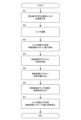
- FIG. 4 is a flowchart showing the operation flow of the electronic tag.
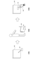
- FIG. 5 is a diagram for explaining how to use an electronic tag.
- FIG. 6 is a schematic configuration diagram showing another example of the sensor.
- FIG. 7 is a diagram for explaining another example of a state in which the sensor is tilted.
- the RTC 20, the latch circuit 40, the control circuit 50, and the memory 60 can each be provided as an IC (Integrated Circuit) chip. Further, some or all of these multiple configurations may be mounted on one IC package.
- IC Integrated Circuit
- the RTC 20 has a clock function.
- the RTC 20 is electrically connected to the battery 10 so that power is constantly supplied.
- the RTC 20 always measures time while power is being supplied.
- the sensor 30 is a mechanical shock sensor configured to be energized when an acceleration (impact) whose absolute value is equal to or greater than a predetermined acceleration is applied, and not energized when an acceleration whose absolute value is equal to or greater than a predetermined acceleration is not applied. It is a sensor. The sensor 30 does not consume the power of the battery 10 unless an acceleration whose absolute value is equal to or greater than a predetermined acceleration is applied. The sensor 30 will be explained in detail later.
- the latch circuit 40 is electrically connected to the battery 10, the sensor 30, and the control circuit 50.
- the latch circuit 40 enters the ON state to supply power to the control circuit 50 when the sensor 30 is energized, and maintains the ON state even if the sensor 30 is subsequently de-energized.
- the latch circuit 40 receives a control signal (power OFF signal) from the control circuit 50, it enters an OFF state in which no power is supplied to the control circuit 50.
- the latch circuit 40 does not consume power from the battery 10 in the OFF state.
- the latch circuit 40 will be explained in detail later.
- the control circuit 50 is electrically connected to the RTC 20, the latch circuit 40, the memory 60, and the antenna 70. When power is supplied from the latch circuit 40 to the control circuit 50, power is also supplied to the memory 60 via the control circuit 50. When the latch circuit 40 is turned on, power may be directly supplied from the latch circuit 40 to the memory 60.
- the control circuit 50 acquires the time from the RTC 20 and writes the acquired time into the memory 60.
- the memory 60 is a non-volatile memory that retains written storage contents even when power is not supplied.
- the memory 60 also stores non-rewritable information.
- the non-rewritable information is, for example, identification information of the electronic tag 100.
- the electronic tag 100 may be a BLE tag that employs the BLUETOOTH (registered trademark) Low Energy (BLE) communication method, which is a low power consumption communication mode.
- BLUETOOTH registered trademark
- BLE Low Energy
- the senor 30 is a so-called three-axis sensor that can detect impacts in the X-axis direction, Y-axis direction, and Z-axis direction.
- the senor 30 includes a case 31, a movable body 32 housed in the case 31, and a plurality of biasing members provided between the case 31 and the movable body 32 to support the movable body 32.
- a spring 33 and fixed electrodes Pa to Pf are provided.
- the case 31 is a hollow hexahedron.
- One fixed electrode (Pa to Pf) is provided on each of the six inner planes of the case 31.
- the fixed electrode Pe is an electrode provided on the inner plane of the case 31 on the front side of the paper
- the fixed electrode Pf is an electrode provided on the inner plane of the case 31 on the back side of the paper.
- the fixed electrodes Pa to Pf are connected to the ground (GND) via a latch circuit 40.
- the movable body 32 has movable electrodes 32a to 32f formed at positions corresponding to (opposed to) the fixed electrodes Pa to Pf, respectively.
- the movable electrode 32e is an electrode provided at a position corresponding to (opposed to) the fixed electrode Pe
- the movable electrode 32f is an electrode provided at a position corresponding to (opposed to) the fixed electrode Pf.
- the movable body 32 is made of a conductive material such as an iron-based material, and is connected to the positive electrode (Vcc) of the battery 10 via a latch circuit 40.
- the movable body 32 is supported by a plurality of springs 33 such that when the sensor 30 is stationary, each of the movable electrodes 32a to 32f is spaced apart from each of the fixed electrodes Pa to Pf.
- the movable body 32 When acceleration is applied to the sensor 30, the movable body 32 is displaced relative to the case 31 against the urging force of the plurality of springs 33 due to inertial force. The movable body 32 is displaced relative to the case 31 whether the acceleration applied to the sensor 30 is positive acceleration or negative acceleration (deceleration).
- the movable body 32 when positive acceleration in the positive direction of the X-axis is applied to the sensor 30, the movable body 32 is displaced relative to the case 31 so that the movable electrode 32b and the fixed electrode Pb approach. Further, when negative acceleration in the positive direction of the X-axis is applied to the sensor 30, the movable body 32 is displaced relative to the case 31 so that the movable electrode 32d and the fixed electrode Pd approach each other. In this way, when acceleration is applied to the sensor 30, at least one movable electrode (32a to 32f) is displaced relative to the case 31 so as to approach the corresponding (opposed) fixed electrode (Pa to Pf). .
- the plurality of springs 33 are configured such that when an acceleration whose absolute value is equal to or greater than a predetermined acceleration is applied to the sensor 30, the movable electrodes (32a to 32f) and the fixed electrodes (Pa to Pf) come into contact and the sensor 30 is brought into a conductive state.
- the spring constant is set so that
- the predetermined acceleration can be set to a desired acceleration as appropriate by changing the spring constants of the plurality of springs 33 or by changing the shape and weight of the movable body 32. Further, although four springs 33 are shown in FIG. 2, the shape, arrangement, and number of the springs 33 can be changed as appropriate. For example, the number of springs 33 may be one.
- the movable electrodes (32a to 32f) and the fixed electrodes (Pa to Pf) come into contact and become electrically conductive. Further, the sensor 30 is located at a position where the movable electrodes (32a to 32f) and the fixed electrodes (Pa to Pf) are separated by the biasing force of the plurality of springs 33 when an acceleration whose absolute value is not less than a predetermined acceleration is not applied.
- the movable body 32 is supported and becomes non-conductive.
- the senor 30 becomes conductive and energized when an acceleration whose absolute value is equal to or greater than a predetermined acceleration is applied, and becomes non-conductive when the absolute value of the applied acceleration decreases and falls below the predetermined acceleration.
- the power supply is cut off.
- the fact that the sensor 30 is energized means that the sensor 30 has detected an impact.
- the senor 30 can be configured such that when the sensor 30 is in a tilted posture of a predetermined tilt or more, the sensor 30 is connected to the movable body 32.
- the fixed electrodes may be in contact with each other to be electrically conductive.
- the senor 30 may be configured to be in a conductive state and energized both when an acceleration whose absolute value is equal to or greater than a predetermined acceleration is applied and when the sensor is in a tilted posture equal to or greater than a predetermined inclination.
- the movable electrodes (32a to 32f) and the fixed electrodes (Pa to Pf) are electrically connected, and at the same time the movable electrodes and the fixed electrodes in two or more directions are connected.
- the memory 60 may record that the sensor 30 is tilted at a predetermined tilt or higher when the two are electrically connected. By providing one electric wire (signal line) for one fixed electrode, it is possible to determine which fixed electrode is energized.
- FIG. 3 is a circuit diagram showing an example of the latch circuit 40.
- the latch circuit 40 includes transistors Tr1 to Tr4, resistors R1 to R11, and a capacitor C1.
- the latch circuit 40 is an electronic circuit that does not have mechanical moving parts.
- the path for supplying power from the battery 10 to the sensor 30 is built into the latch circuit 40. That is, the energizing circuit L that supplies power from the battery 10 to the sensor 30 constitutes a part of the latch circuit 40.
- transistor Tr2 When transistor Tr2 is turned off, transistor Tr3 is turned off. This stops the current flowing to the control circuit 50 (OFF state).
- the electronic tag 100 is configured so that power is supplied to the control circuit 50 and memory 60 only while the sensor 30 is energized, the control circuit 50 completes writing the time to the memory 60. There is a possibility that the power supply to the control circuit 50 and the memory 60 will be stopped before. In this case, the time at which the sensor 30 detects the impact cannot be recorded in the memory 60.
- the latch circuit 40 by providing the latch circuit 40, the supply of power to the control circuit 50 and the memory 60 is maintained until the control circuit 50 completes writing the time to the memory 60. . After the control circuit 50 completes writing the time into the memory 60, the latch circuit 40 is turned off, so that the latch circuit 40, the control circuit 50, and the memory 60 no longer consume power. Therefore, while suppressing the consumption of the battery 10, it is possible to prevent a failure in which the sensor 30 cannot record the time when the impact is detected.
- the energization circuit L that supplies power from the battery 10 to the sensor 30 constitutes a part of the latch circuit 40.
- the senor 30 detects the impact and is energized, and the latch circuit 40 is activated to supply power to the control circuit 50.
- the current flowing through the energizing circuit L functions as a detection signal indicating that the sensor 30 has detected an impact.
- the period from when the sensor 30 detects an impact until the latch circuit 40 supplies power to the control circuit 50 is The time lag can be reduced. This reduces the time lag until the control circuit 50 acquires the time from the RTC 20, thereby increasing the reliability of the time stored in the memory 60. Furthermore, since the time it takes for the latch circuit 40 to turn off is also shortened, consumption of the battery 10 can be suppressed.
- FIG. 4 is a flowchart showing the operation flow of the electronic tag 100.
- step S01 an acceleration whose absolute value is greater than or equal to a predetermined acceleration is applied to the electronic tag 100 (sensor 30).
- step S02 the sensor 30 becomes conductive and energized.
- step S03 the latch circuit 40 is turned on and power is supplied from the latch circuit 40 to the control circuit 50 and the memory 60.
- step S04 the control circuit 50 acquires the time from the RTC 20.
- step S05 the control circuit 50 writes the acquired time into the memory 60.
- step S06 the control circuit 50 outputs a control signal to the latch circuit 40.
- step S07 the latch circuit 40 is turned off and the supply of power from the latch circuit 40 to the control circuit 50 and memory 60 is stopped.
- FIG. 5 is a diagram for explaining how to use the electronic tag 100.
- step 1 the electronic tag 100 is attached to the portable article 200.
- the portable articles 200 are various articles that can be transported and to which the electronic tags 100 can be attached.
- the electronic tag 100 may be attached to the portable article 200 with double-sided tape, or may be attached to the portable article 200 using a special jig, or the tag body 110 may be provided with an attachment hole to attach it to the portable article 200. 200 may be screwed.
- step 2 an impact is applied to the portable article 200 to which the electronic tag 100 is attached.
- the electronic tag 100 stores in the memory 60 the time when the sensor 30 detects the impact.
- FIG. 5 shows how negative acceleration is applied to the transportable article 200 due to the fall.
- the electronic tag 100 detects an impact multiple times, it stores all of the times at which the impact was detected in the memory 60.
- step 3 the reader/writer 300 is used to read the information stored in the memory 60.
- the electronic tag 100 is operated by the installed battery 10 and is used by being attached to a portable article 200.
- the electronic tag 100 includes an RTC 20 that is constantly supplied with power from the battery 10 and outputs the time, a control circuit 50 that is connected to the RTC 20, and a control circuit 50 that is connected to the battery 10 so that power is directly supplied from the battery 10, and that outputs the absolute value.
- the sensor 30 which becomes conductive and energized when an acceleration of a predetermined acceleration or more is applied, and when the sensor 30 is energized, it becomes an ON state that supplies power to the control circuit 50, and then the sensor 30 is turned on.
- the control circuit 50 includes a latch circuit 40 that maintains an ON state even if it becomes a non-conducting state and the power is cut off, and when power is supplied, the control circuit 50 acquires the time from the RTC 20 and writes it in the memory 60, and then, A control signal is output to the latch circuit 40 to turn the latch circuit 40 into an OFF state in which no power is supplied to the control circuit 50 .
- the sensor 30 and the control circuit 50 do not consume the power of the battery 10 unless an acceleration whose absolute value is equal to or greater than a predetermined acceleration is applied. That is, the configuration other than the RTC 20 does not consume the power of the battery 10 unless an acceleration whose absolute value is equal to or greater than a predetermined acceleration is applied. Therefore, the time at which an impact was detected can be recorded while saving power.
- the sensor 30 includes a case 31 , a movable body 32 housed in the case 31 , at least one spring 33 provided between the case 31 and the movable body 32 and supporting the movable body 32 , and a spring 33 provided in the case 31 .
- the movable body 32 includes fixed electrodes Pa to Pf, and is electrically connected to the battery 10.
- the senor 30 does not consume power when the movable body 32 and the fixed electrodes (Pa to Pf) are separated from each other. Therefore, consumption of the battery 10 can be suppressed.
- the senor 30 does not consume power in a state where an acceleration whose absolute value is equal to or greater than the predetermined acceleration is not applied. Therefore, consumption of the battery 10 can be suppressed.
- the sensor 30 includes movable electrodes (32a to 32f) and fixed electrodes (Pa to Pf) that come into contact with each other to bring the sensor 30 into a conductive state when an acceleration whose absolute value is equal to or greater than a predetermined acceleration is applied.
- the senor 30 does not consume power when the movable electrodes (32a to 32f) and the fixed electrodes (Pa to Pf) are separated from each other. Therefore, consumption of the battery 10 can be suppressed.
- the latch circuit 40 is an electronic circuit with no moving parts.
- the time lag from when the sensor 30 detects an impact until the latch circuit 40 supplies power to the control circuit 50 can be reduced compared to the case where the latch circuit 40 has a movable part. This reduces the time lag until the control circuit 50 acquires the time from the RTC 20, thereby increasing the reliability of the time stored in the memory 60. Furthermore, since the time it takes for the latch circuit 40 to turn off is also shortened, consumption of the battery 10 can be suppressed.
- the energizing circuit L that supplies power from the battery 10 to the sensor 30 constitutes a part of the latch circuit 40.
- the period from when the sensor 30 detects an impact until the latch circuit 40 supplies power to the control circuit 50 is The time lag can be reduced. This reduces the time lag until the control circuit 50 acquires the time from the RTC 20, thereby increasing the reliability of the time stored in the memory 60. Furthermore, since the time it takes for the latch circuit 40 to turn off is also shortened, consumption of the battery 10 can be suppressed.
- the electronic tag 100 is a wireless communication tag (RFID tag, BLE tag) that has an antenna 70 connected to a control circuit 50.
- RFID tag RFID tag, BLE tag
- the time etc. stored in the memory 60 can be easily read using the reader/writer 300.
- the configurations other than the RTC 20 consume the power of the battery 10 only when necessary (not always consumed), so the consumption of the battery 10 by the configurations other than the RTC 20 can be suppressed.
- the structure of the sensor included in the electronic tag 100 is not limited to the structure shown in FIG. 2.
- the sensor may have any structure as long as the movable body (movable electrode) and the fixed electrode come into contact and the sensor becomes conductive when some kind of displacement occurs in the object to which the electronic tag 100 is attached.
- FIG. 6 is a schematic configuration diagram showing a sensor 80 as another example of the sensor included in the electronic tag 100.
- the sensor 80 includes a case 81, a movable body (movable electrode) 82 housed in the case 81, a spring 83 as a biasing member provided between the case 81 and the movable body 82, and supporting the movable body 82. , fixed electrodes Pg, Ph.
- the movable body 82 is suspended by a spring 83.
- the electronic tag 100 including the sensor 80 is attached to an object so that the orientation of the sensor 80 matches the direction of gravity.
- the state in which the orientation of the sensor 80 matches the direction of gravity is a state in which the sensor 80 is arranged so that the negative direction of the Y-axis in FIG. 6 matches the direction of gravity.
- the senor 80 is configured such that when the sensor 80 is tilted at a predetermined tilt position or higher, the movable body 82 and either of the fixed electrodes (Pg, Ph) come into contact and become electrically conductive. There is.
- the movable body 82 causes the spring 83 to deflect due to inertial force, and is displaced relative to the case 31. Therefore, the sensor 80 can also detect that an impact is applied.
Landscapes
- Engineering & Computer Science (AREA)
- Physics & Mathematics (AREA)
- General Physics & Mathematics (AREA)
- Computer Hardware Design (AREA)
- Microelectronics & Electronic Packaging (AREA)
- Theoretical Computer Science (AREA)
- Power Sources (AREA)
- Burglar Alarm Systems (AREA)
- Electric Clocks (AREA)
Abstract
電子タグは、電池から電力が常時供給され、時刻を出力するリアルタイムクロックと、リアルタイムクロックと接続される制御回路と、電池から電力が直接供給されるように電池と接続され、絶対値が所定加速度以上の加速度が印加されると導通状態になり通電するセンサと、センサと接続され、センサが通電すると制御回路に電力を供給するON状態になり、その後にセンサが非導通状態になって通電が遮断されてもON状態を維持するラッチ回路と、を備え、制御回路は、電力が供給されるとリアルタイムクロックから時刻を取得してメモリに書き込み、その後、ラッチ回路を制御回路に電力を供給しないOFF状態にする制御信号をラッチ回路に出力する。
Description
本発明は、電子タグに関する。
JP2010-197111Aには、電子機器に取り付けられて輸送時の衝撃等のイベントを記録するイベント記録装置が開示されている。
上記のイベント記録装置は、衝撃センサの衝撃感知に伴う一定量以上の電荷発生をトリガとして電池からマイコンへの給電を開始する給電スイッチを有する。
マイコンは、給電開始後、衝撃センサによるイベントの検知を、電子機器のマザーボード上に実装されているリアルタイムクロックから取得した時刻とともに不揮発メモリに記録する。
上記のイベント記録装置は、給電スイッチが衝撃センサの電荷発生をトリガとして作動するものであることから、電荷を増幅させる増幅回路が必要となる。この場合は、増幅回路に常時電源を投入する必要があるので、消費電力が大きいという問題がある。
本発明は、このような技術的課題に鑑みてなされたもので、省電力で衝撃を検知した時刻を記録できるようにすることを目的とする。
本発明のある態様によれば、搭載された電池によって作動し、可搬物品に取り付けて使用される電子タグであって、前記電池から電力が常時供給され、時刻を出力するリアルタイムクロックと、前記リアルタイムクロックと接続される制御回路と、前記電池から前記電力が直接供給されるように前記電池と接続され、絶対値が所定加速度以上の加速度が印加されると導通状態になり通電するセンサと、前記センサと接続され、前記センサが通電すると前記制御回路に前記電力を供給するON状態になり、その後に前記センサが非導通状態になって通電が遮断されても前記ON状態を維持するラッチ回路と、を備え、前記制御回路は、前記電力が供給されると前記リアルタイムクロックから時刻を取得してメモリに書き込み、その後、前記ラッチ回路を前記制御回路に前記電力を供給しないOFF状態にする制御信号を前記ラッチ回路に出力する、電子タグが提供される。
上記態様によれば、センサ及び制御回路は、絶対値が所定加速度以上の加速度が印加されなければ電池の電力を消費しない。よって、省電力で衝撃を検知した時刻を記録できる。
以下、添付図面を参照しながら本発明の実施形態に係る電子タグ100について説明する。
図1は、電子タグ100の概略構成図である。図1において、実線の矢印は電力の流れを示し、破線の矢印は信号の流れを示している。
図1に示すように、電子タグ100は、電池10と、リアルタイムクロック(以下、RTCという。)20と、センサ30と、ラッチ回路40と、制御回路50と、メモリ60と、アンテナ70と、を備える。
RTC20、ラッチ回路40、制御回路50、メモリ60は、それぞれIC(Integrated Circuit)チップとして設けることができる。また、これら複数の構成のうちのいくつか又は全てを1つのICパッケージに搭載してもよい。
電子タグ100は、上記の各構成を実装した基板を樹脂製のタグボディ110に収容して構成される。基板は、リジッド基板であってもよいし、フレキシブル基板であってもよい。電子タグ100のサイズは、長手方向が数十[mm]程度であり、厚さ方向が数[mm]程度である。
電池10としては、例えば、ボタン電池を採用することができる。
RTC20は、時計機能を有する。RTC20は、電力が常時供給されるように電池10と電気的に接続される。RTC20は、電力が供給されている間は、常に時刻を計時している。
センサ30は、電線S1、S2によってラッチ回路40と接続され、ラッチ回路40を介して電池10と電気的に接続される。本実施形態では、電池10からセンサ30に電力を供給する経路は、ラッチ回路40に組み込まれている。
センサ30は、絶対値が所定加速度以上の加速度(衝撃)が印加されている状態では通電し、絶対値が所定加速度以上の加速度が印加されていない状態では通電しないように構成されたメカニカルな衝撃センサである。センサ30は、絶対値が所定加速度以上の加速度が印加されていない状態では電池10の電力を消費しない。センサ30については後で詳しく説明する。
ラッチ回路40は、電池10、センサ30、及び制御回路50と電気的に接続されている。
ラッチ回路40は、センサ30が通電すると制御回路50に電力を供給するON状態になり、その後にセンサ30の通電が遮断されてもON状態を維持する。ラッチ回路40は、制御回路50から制御信号(電源OFF信号)を受信すると制御回路50に電力を供給しないOFF状態になる。ラッチ回路40は、OFF状態では電池10の電力を消費しない。ラッチ回路40については後で詳しく説明する。
制御回路50は、RTC20、ラッチ回路40、メモリ60、及びアンテナ70と電気的に接続されている。ラッチ回路40から制御回路50に電力が供給されると、制御回路50を介してメモリ60にも電力が供給される。ラッチ回路40がON状態になるとラッチ回路40からメモリ60に電力が直接供給されるようにしてもよい。
制御回路50は、ラッチ回路40から電力が供給されると、RTC20から時刻を取得し、取得した時刻をメモリ60に書き込む。
すなわち、センサ30に絶対値が所定加速度以上の加速度(衝撃)が印加されることでセンサ30が通電してラッチ回路40から制御回路50に電力が供給されると、制御回路50は、センサ30に加速度(衝撃)が印加されたときの時刻をRTC20から取得する。
例えば、制御回路50の処理能力が不十分である等の影響により、センサ30に加速度(衝撃)が印加されてから制御回路50がRTC20から時刻を取得するまでにタイムラグがある場合は、そのタイムラグ分を制御回路50で補正することで、センサ30に加速度(衝撃)が印加されたときの時刻を実質的に得ることができる。
制御回路50は、メモリ60への時刻の書き込みが完了すると、ラッチ回路40に制御信号を出力してラッチ回路40を制御回路50及びメモリ60に電力を供給しないOFF状態にする。これにより、制御回路50及びメモリ60への電力の供給が停止される。制御回路50及びメモリ60は、ラッチ回路40がOFF状態では電池10の電力を消費しない。
メモリ60は、電力が供給されていない状態でも書き込まれた記憶内容を保持する不揮発性のメモリである。
アンテナ70は、リーダライタ300(図5参照)から発せられる電波を受けることで制御回路50及びメモリ60を動作させるための電力を発生させる。制御回路50は、アンテナ70が発生させた電力を用いてメモリ60に書き込まれた情報を読み出し、読み出した情報をアンテナ70からリーダライタ300に送る。
リーダライタ300を用いてメモリ60に記憶されている情報を書き換えることも可能である。なお、メモリ60には、書き換え不能な情報も記憶されている。書き換え不能な情報は、例えば、電子タグ100の識別情報である。
このように、本実施形態の電子タグ100は、RFID(Radio Frequency Identification)技術に対応した無線通信タグ(RFIDタグ)として構成される。
電子タグ100は、低消費電力の通信モードであるBLUETOOTH(登録商標) Low Energy(BLE)の通信方式を採用したBLEタグとしてもよい。
続いて、図2を参照しながらセンサ30について説明する。
図2は、センサ30の一例を示す概略構成図である。
図2の例では、センサ30は、X軸方向、Y軸方向、Z軸方向の衝撃を検知することができる所謂3軸センサである。
図2に示すように、センサ30は、ケース31と、ケース31に収容された可動体32と、ケース31と可動体32との間に設けられて可動体32を支持する複数の付勢部材としてのばね33と、固定電極Pa~Pfと、を備える。
ケース31は、中空の六面体である。ケース31の6つの内側平面には、各面に1つずつ固定電極(Pa~Pf)が設けられる。図2において、固定電極Peは、ケース31における紙面手前側の内側平面に設けられた電極であり、固定電極Pfは、紙面奥側の内側平面に設けられた電極である。
固定電極Pa~Pfは、ラッチ回路40を介してグランド(GND)と接続される。
可動体32は、固定電極Pa~Pfそれぞれに対応(対向)する位置に形成された可動電極32a~32fを有する。図2において、可動電極32eは、固定電極Peに対応(対向)する位置に設けられた電極であり、可動電極32fは、固定電極Pfに対応(対向)する位置に設けられた電極である。
可動体32は鉄系材料等の導電性材料で形成されており、ラッチ回路40を介して電池10のプラス極(Vcc)と接続される。
可動体32は、センサ30が静止している状態では、可動電極32a~32fのそれぞれが固定電極Pa~Pfのそれぞれから離間するように、複数のばね33に支持される。
可動体32は、センサ30に加速度が印加されると、慣性力によって複数のばね33の付勢力に抗してケース31に対して相対変位する。可動体32は、センサ30に印加される加速度が正の加速度であっても負の加速度(減速度)であってもケース31に対して相対変位する。
例えば、センサ30にX軸正方向の正の加速度が印加されると、可動体32は、可動電極32bと固定電極Pbとが近づくようにケース31に対して相対変位する。また、センサ30にX軸正方向の負の加速度が印加されると、可動体32は、可動電極32dと固定電極Pdとが近づくようにケース31に対して相対変位する。このように、センサ30に加速度が印加されると、少なくとも1つの可動電極(32a~32f)が、対応(対向)する固定電極(Pa~Pf)に近づくようにケース31に対して相対変位する。
複数のばね33は、センサ30に絶対値が所定加速度以上の加速度が印加されている状態で可動電極(32a~32f)と固定電極(Pa~Pf)とが接触してセンサ30が導通状態となるように、ばね定数が設定される。
よって、例えば、センサ30にX軸正方向の所定加速度以上の正の加速度が印加されると、可動電極32bと固定電極Pbとが接触する。また、センサ30にX軸正方向の絶対値が所定加速度以上の負の加速度が印加されると、可動電極32dと固定電極Pdとが接触する。
所定加速度は、複数のばね33のばね定数を変更することや、可動体32の形状や重量を変更することで、適宜所望の加速度に設定可能である。また、図2では、4つのばね33が示されているが、ばね33の形状、配置、数については適宜変更可能である。例えば、ばね33の数は、1つであってもよい。
このように、センサ30は、絶対値が所定加速度以上の加速度が印加されている状態では、可動電極(32a~32f)と固定電極(Pa~Pf)とが接触して導通状態になる。また、センサ30は、絶対値が所定加速度以上の加速度が印加されていない状態では、複数のばね33の付勢力によって可動電極(32a~32f)と固定電極(Pa~Pf)とが離間する位置に可動体32が支持されて非導通状態になる。
つまり、センサ30は、絶対値が所定加速度以上の加速度が印加されると導通状態になって通電し、その後に印加されている加速度の絶対値が減少して所定加速度を下回ると非導通状態になって通電が遮断される。センサ30が通電することは、センサ30が衝撃を検知したことを意味する。
また、センサ30は、例えば、水平方向に対して1つまたは複数のばね33のばね定数を弱く設定することで、センサ30が所定傾斜以上の傾斜姿勢になった場合に可動体32といずれかの固定電極(Pa~Pf)とが接触して導通状態になるように構成してもよい。
つまり、センサ30は、絶対値が所定加速度以上の加速度が印加された場合と所定傾斜以上の傾斜姿勢になった場合との両方において導通状態になり通電するように構成してもよい。
この場合、可動電極(32a~32f)と固定電極(Pa~Pf)とがX軸・Y軸・Z軸のいずれの方向で導通したのかを判定し、同時に2方向以上の稼働電極と固定電極とが導通していた場合に、センサ30が所定傾斜以上の傾斜姿勢になったことをメモリ60に記録するようにしてもよい。1つの固定電極に対して1つの電線(信号線)を設けることで、どの固定電極が通電したかを判定することができる。
続いて、図3を参照しながらラッチ回路40について説明する。
図3は、ラッチ回路40の一例を示す回路図である。
図3に示すように、ラッチ回路40は、トランジスタTr1~Tr4と、抵抗R1~R11と、コンデンサC1と、を備える。ラッチ回路40は、メカニカルな可動部を有しない電子回路である。
上述したように、本実施形態では、電池10からセンサ30に電力を供給する経路は、ラッチ回路40に組み込まれている。すなわち、電池10からセンサ30に電力を供給する通電回路Lは、ラッチ回路40の一部を構成する。
ラッチ回路40は、センサ30が導通状態になって通電回路Lに電流が流れると、トランジスタTr1がONになる。
トランジスタTr1がONになると、トランジスタTr1のコレクタから電流がトランジスタTr2のベースに流れてトランジスタTr2がONになる。
トランジスタTr2がONになると、トランジスタTr3がONになる。
トランジスタTr3がONになると、トランジスタTr3のコレクタから電流が制御回路50に流れる。また、トランジスタTr3のコレクタから分岐された電流がトランジスタTr2のベースに流れることで、制御回路50に電流が流れる状態が維持される(ON状態)。これにより、センサ30が非導通状態になって通電回路Lに電流が流れなくなっても、制御回路50には電流が流れる。
ON状態のラッチ回路40に対して制御回路50から制御信号が入力されると、トランジスタTr4がONになる。
トランジスタTr4がONになると、トランジスタTr1のコレクタ電流がGNDに流れてトランジスタTr2がOFFになる。
トランジスタTr2がOFFになると、トランジスタTr3がOFFになる。これにより、制御回路50への電流が止まる(OFF状態)。
上述したように、センサ30は、絶対値が所定加速度以上の加速度が印加されると導通状態になって通電し、その後に印加されている加速度の絶対値が減少して所定加速度を下回ると非導通状態になって通電が遮断される。
そのため、仮に、センサ30が通電している間のみ制御回路50及びメモリ60に電力が供給されるように電子タグ100を構成した場合は、制御回路50がメモリ60への時刻の書き込みを完了する前に制御回路50及びメモリ60への電力の供給が停止する可能性がある。この場合は、センサ30が衝撃を検知した時刻をメモリ60に記録することができない。
これに対して、本実施形態では、ラッチ回路40を設けることで、制御回路50がメモリ60への時刻の書き込みを完了するまでは、制御回路50及びメモリ60への電力の供給が維持される。そして、制御回路50がメモリ60への時刻の書き込みを完了した後は、ラッチ回路40がOFF状態になることで、ラッチ回路40、制御回路50、及びメモリ60が電力を消費しなくなる。よって、電池10の消費を抑制しつつ、センサ30が衝撃を検知した時刻を記録できないフェイルの発生を防止できる。
また、本実施形態では、センサ30に電池10から電力を供給する通電回路Lが、ラッチ回路40の一部を構成している。
そのため、センサ30が衝撃を検知して通電するとともにラッチ回路40が作動して制御回路50に電力が供給される。つまり、通電回路Lを流れる電流は、センサ30が衝撃を検知したことを示す検知信号として機能する。
これによれば、センサ30からラッチ回路40に検知信号を別途送信する必要がない。そのため、センサ30からラッチ回路40に検知信号を別途送信することでラッチ回路40を作動させる場合と比べて、センサ30が衝撃を検知してからラッチ回路40が制御回路50に電力を供給するまでのタイムラグを小さくできる。これにより、制御回路50がRTC20から時刻を取得するまでのタイムラグも小さくなるので、メモリ60に記憶した時刻の信頼性が高くなる。また、ラッチ回路40がOFF状態になるまでの時間も短くなるので、電池10の消費を抑制できる。
続いて、図4を参照しながら電子タグ100の作動手順について説明する。図4は、電子タグ100の作動の流れを示すフローチャートである。
ステップS01では、電子タグ100(センサ30)に絶対値が所定加速度以上の加速度が印加される。
ステップS02では、センサ30が導通状態になって通電する。
ステップS03では、ラッチ回路40がON状態になるとともにラッチ回路40から制御回路50及びメモリ60に電力が供給される。
ステップS04では、制御回路50がRTC20から時刻を取得する。
ステップS05では、制御回路50がメモリ60に取得した時刻を書き込む。
ステップS06では、制御回路50がラッチ回路40に制御信号を出力する。
ステップS07では、ラッチ回路40がOFF状態になるとともにラッチ回路40から制御回路50及びメモリ60への電力の供給が停止される。
続いて、図5を参照しながら電子タグ100の使用方法について説明する。図5は、電子タグ100の使用方法について説明するための図である。
手順1では、可搬物品200に電子タグ100を取り付ける。可搬物品200は、搬送が可能であって電子タグ100を取り付けることができる様々な物品である。
電子タグ100は、例えば、両面テープで可搬物品200に取り付けてもよいし、専用の治具等によって可搬物品200に取り付けてもよいし、タグボディ110に取付孔を設けて可搬物品200にねじ止めしてもよい。
手順2では、電子タグ100を取り付けた可搬物品200に衝撃が印加される。電子タグ100は、センサ30によって衝撃を検知した時刻をメモリ60に記憶する。図5は、落下により可搬物品200に負の加速度が印加される様子を示している。
電子タグ100は、衝撃を複数回検知した場合は、衝撃を検知した複数の時刻を全てメモリ60に記憶する。
手順3では、リーダライタ300を用いてメモリ60に記憶された情報を読み取る。
以上のように構成された電子タグ100の主な作用効果についてまとめて説明する。
電子タグ100は、搭載された電池10によって作動し、可搬物品200に取り付けて使用される。電子タグ100は、電池10から電力が常時供給され、時刻を出力するRTC20と、RTC20と接続される制御回路50と、電池10から電力が直接供給されるように電池10と接続され、絶対値が所定加速度以上の加速度が印加されると導通状態になり通電するセンサ30と、センサ30と接続され、センサ30が通電すると制御回路50に電力を供給するON状態になり、その後にセンサ30が非導通状態になって通電が遮断されてもON状態を維持するラッチ回路40と、を備え、制御回路50は、電力が供給されるとRTC20から時刻を取得してメモリ60に書き込み、その後、ラッチ回路40を制御回路50に電力を供給しないOFF状態にする制御信号をラッチ回路40に出力する。
これによれば、センサ30及び制御回路50は、絶対値が所定加速度以上の加速度が印加されなければ電池10の電力を消費しない。つまり、RTC20以外の構成は、絶対値が所定加速度以上の加速度が印加されなければ電池10の電力を消費しない。よって、省電力で衝撃を検知した時刻を記録できる。
センサ30は、ケース31と、ケース31に収容された可動体32と、ケース31と可動体32との間に設けられ、可動体32を支持する少なくとも1つのばね33と、ケース31に設けられた固定電極Pa~Pfと、を備え、可動体32は、電池10と電気的に接続されている。
これによれば、センサ30は、可動体32と固定電極(Pa~Pf)とが離間している状態では、電力を消費しない。よって、電池10の消費を抑制できる。
センサ30は、絶対値が所定加速度以上の加速度が印加されていない状態では非導通状態である。
これによれば、センサ30は、絶対値が所定加速度以上の加速度が印加されていない状態では、電力を消費しない。よって、電池10の消費を抑制できる。
センサ30は、絶対値が所定加速度以上の加速度が印加されている状態で接触してセンサ30を導通状態にする可動電極(32a~32f)及び固定電極(Pa~Pf)を有する。
これによれば、センサ30は、可動電極(32a~32f)と固定電極(Pa~Pf)とが離間している状態では、電力を消費しない。よって、電池10の消費を抑制できる。
ラッチ回路40は、可動部を有しない電子回路である。
これによれば、ラッチ回路40が可動部を有する場合と比べて、センサ30が衝撃を検知してからラッチ回路40が制御回路50に電力を供給するまでのタイムラグを小さくできる。これにより、制御回路50がRTC20から時刻を取得するまでのタイムラグも小さくなるので、メモリ60に記憶した時刻の信頼性が高くなる。また、ラッチ回路40がOFF状態になるまでの時間も短くなるので、電池10の消費を抑制できる。
センサ30に電池10から電力を供給する通電回路Lは、ラッチ回路40の一部を構成する。
これによれば、センサ30からラッチ回路40に検知信号を別途送信する必要がない。そのため、センサ30からラッチ回路40に検知信号を別途送信することでラッチ回路40を作動させる場合と比べて、センサ30が衝撃を検知してからラッチ回路40が制御回路50に電力を供給するまでのタイムラグを小さくできる。これにより、制御回路50がRTC20から時刻を取得するまでのタイムラグも小さくなるので、メモリ60に記憶した時刻の信頼性が高くなる。また、ラッチ回路40がOFF状態になるまでの時間も短くなるので、電池10の消費を抑制できる。
電子タグ100は、制御回路50と接続されたアンテナ70を有する無線通信タグ(RFIDタグ、BLEタグ)である。
これによれば、リーダライタ300を用いてメモリ60に記憶された時刻等を容易に読み取ることができる。
RTC20のみが電池10の電力を常時消費する。
これによれば、RTC20以外の構成は、電池10の電力を必要なときにしか消費しない(常時消費ではない)ので、RTC20以外の構成による電池10の消費を抑制できる。
以上、本発明の実施形態について説明したが、上記実施形態は本発明の適用例の一つを示したものに過ぎず、本発明の技術的範囲を上記実施形態の具体的構成に限定する趣旨ではない。
例えば、電子タグ100が備えるセンサの構造は、図2に示す構造に限定されるものではない。センサは、電子タグ100が取り付けられた物体に何らかの変位が発生した場合に、可動体(可動電極)と固定電極とが接触してセンサが導通状態になる構造であればよい。
図6は、電子タグ100が備えるセンサの他の例としてのセンサ80を示す概略構成図である。センサ80は、ケース81と、ケース81に収容された可動体(可動電極)82と、ケース81と可動体82との間に設けられて可動体82を支持する付勢部材としてのばね83と、固定電極Pg、Phと、を備える。センサ80では、可動体82は、ばね83に吊るされている。
センサ80を備える電子タグ100は、センサ80の向きが重力方向と一致するように、物体に取り付けられる。センサ80の向きが重力方向と一致する状態とは、具体的には、図6におけるY軸のマイナス方向と重力方向とが一致するようにセンサ80を配置した状態である。
図7に示すように、センサ80は、ばね83が撓むことにより、所定傾斜以上の傾斜姿勢になった場合に可動体82と固定電極Pgとが接触して導通状態になる。なお、センサ80が図7とは反対方向に傾いた場合は、可動体82と固定電極Phとが接触する。
このように、センサ80は、センサ80が所定傾斜以上の傾斜姿勢になった場合に可動体82といずれかの固定電極(Pg、Ph)とが接触して導通状態になるように構成されている。
また、可動体82は、センサ80に加速度が印加された場合に、慣性力によってばね83に撓みを発生させてケース31に対して相対変位する。よって、センサ80は、衝撃が印加されたことも検知できる。
本願は2022年7月7日に日本国特許庁に出願された特願2022-109864に基づく優先権を主張し、この出願の全ての内容は参照により本明細書に組み込まれる。
Claims (8)
- 搭載された電池によって作動し、可搬物品に取り付けて使用される電子タグであって、
前記電池から電力が常時供給され、時刻を出力するリアルタイムクロックと、
前記リアルタイムクロックと接続される制御回路と、
前記電池から前記電力が直接供給されるように前記電池と接続され、絶対値が所定加速度以上の加速度が印加されると導通状態になり通電するセンサと、
前記センサと接続され、前記センサが通電すると前記制御回路に前記電力を供給するON状態になり、その後に前記センサが非導通状態になって通電が遮断されても前記ON状態を維持するラッチ回路と、
を備え、
前記制御回路は、前記電力が供給されると前記リアルタイムクロックから時刻を取得してメモリに書き込み、その後、前記ラッチ回路を前記制御回路に前記電力を供給しないOFF状態にする制御信号を前記ラッチ回路に出力する、
電子タグ。 - 請求項1に記載の電子タグであって、
前記センサは、
ケースと、
前記ケースに収容された可動体と、
前記ケースと前記可動体との間に設けられ、前記可動体を支持する少なくとも1つの付勢部材と、
前記ケースに設けられた固定電極と、
を備え、
前記可動体は、前記電池と電気的に接続されている、
電子タグ。 - 請求項1に記載の電子タグであって、
前記センサは、絶対値が前記所定加速度以上の加速度が印加されていない状態では前記非導通状態である、
電子タグ。 - 請求項1に記載の電子タグであって、
前記センサは、絶対値が前記所定加速度以上の加速度が印加されている状態で接触して前記センサを前記導通状態にする可動電極及び固定電極を有する、
電子タグ。 - 請求項1に記載の電子タグであって、
前記ラッチ回路は、可動部を有しない電子回路である、
電子タグ。 - 請求項1に記載の電子タグであって、
前記センサに前記電池から前記電力を供給する通電回路は、前記ラッチ回路の一部を構成する、
電子タグ。 - 請求項1に記載の電子タグであって、
前記制御回路と接続されたアンテナを有する無線通信タグである、
電子タグ。 - 請求項1から7のいずれか1つに記載の電子タグであって、
前記リアルタイムクロックのみが前記電池の前記電力を常時消費する、
電子タグ。
Applications Claiming Priority (2)
| Application Number | Priority Date | Filing Date | Title |
|---|---|---|---|
| JP2022-109864 | 2022-07-07 | ||
| JP2022109864A JP2024008198A (ja) | 2022-07-07 | 2022-07-07 | 電子タグ |
Publications (1)
| Publication Number | Publication Date |
|---|---|
| WO2024009792A1 true WO2024009792A1 (ja) | 2024-01-11 |
Family
ID=89453347
Family Applications (1)
| Application Number | Title | Priority Date | Filing Date |
|---|---|---|---|
| PCT/JP2023/023189 Ceased WO2024009792A1 (ja) | 2022-07-07 | 2023-06-22 | 電子タグ |
Country Status (2)
| Country | Link |
|---|---|
| JP (1) | JP2024008198A (ja) |
| WO (1) | WO2024009792A1 (ja) |
Families Citing this family (1)
| Publication number | Priority date | Publication date | Assignee | Title |
|---|---|---|---|---|
| JP2025132877A (ja) * | 2024-02-29 | 2025-09-10 | 株式会社サトー | 衝撃センサ |
Citations (4)
| Publication number | Priority date | Publication date | Assignee | Title |
|---|---|---|---|---|
| JP2005337736A (ja) * | 2004-05-24 | 2005-12-08 | Ubukata Industries Co Ltd | 運搬時衝撃記録装置 |
| JP2006515952A (ja) * | 2003-01-02 | 2006-06-08 | シンベット・コーポレイション | ソリッドステートのバッテリー給電の装置と製法 |
| JP2009016167A (ja) * | 2007-07-04 | 2009-01-22 | Seiko Instruments Inc | モーションスイッチ |
| US20160018431A1 (en) * | 2014-07-18 | 2016-01-21 | University Of Georgia Research Foundation, Inc. | Berry impact recording device |
Family Cites Families (2)
| Publication number | Priority date | Publication date | Assignee | Title |
|---|---|---|---|---|
| JP2010197111A (ja) * | 2009-02-23 | 2010-09-09 | Nec Corp | イベント記録装置及び電子機器 |
| JP5310491B2 (ja) * | 2009-11-05 | 2013-10-09 | 株式会社村田製作所 | 衝撃検出装置 |
-
2022
- 2022-07-07 JP JP2022109864A patent/JP2024008198A/ja active Pending
-
2023
- 2023-06-22 WO PCT/JP2023/023189 patent/WO2024009792A1/ja not_active Ceased
Patent Citations (4)
| Publication number | Priority date | Publication date | Assignee | Title |
|---|---|---|---|---|
| JP2006515952A (ja) * | 2003-01-02 | 2006-06-08 | シンベット・コーポレイション | ソリッドステートのバッテリー給電の装置と製法 |
| JP2005337736A (ja) * | 2004-05-24 | 2005-12-08 | Ubukata Industries Co Ltd | 運搬時衝撃記録装置 |
| JP2009016167A (ja) * | 2007-07-04 | 2009-01-22 | Seiko Instruments Inc | モーションスイッチ |
| US20160018431A1 (en) * | 2014-07-18 | 2016-01-21 | University Of Georgia Research Foundation, Inc. | Berry impact recording device |
Also Published As
| Publication number | Publication date |
|---|---|
| JP2024008198A (ja) | 2024-01-19 |
Similar Documents
| Publication | Publication Date | Title |
|---|---|---|
| JP4313951B2 (ja) | 静電無線周波数識別タグ装置とこれに関連する方法 | |
| US11907897B2 (en) | Transportation data logging device and item transportation system including the same | |
| US4733766A (en) | Coin checking apparatus | |
| US11726151B2 (en) | Magnetic field sensor in a portable electronic device | |
| JP2024008198A (ja) | 電子タグ | |
| JP2005310128A5 (ja) | ||
| JP2024143600A (ja) | 衝撃センサ | |
| KR102421413B1 (ko) | 물품 운송 시스템 | |
| JP5150950B2 (ja) | 情報記録媒体処理装置 | |
| US20070102529A1 (en) | Information devices | |
| JP2025132873A (ja) | 衝撃センサ | |
| JP2025109449A (ja) | 衝撃センサ | |
| JP2013217701A (ja) | 振動検出センサー装置 | |
| JP5779415B2 (ja) | 電子装置の駆動方法 | |
| JP2017078911A (ja) | カード型データ記憶装置 | |
| JP2025132877A (ja) | 衝撃センサ | |
| JP2009512926A (ja) | 完全性を知る必要があるエレメントの識別および保護用デバイス | |
| KR101067887B1 (ko) | Rfid 장치 | |
| KR101218280B1 (ko) | Rfid 장치 | |
| JP2010197111A (ja) | イベント記録装置及び電子機器 | |
| JP2025132878A (ja) | 衝撃センサ | |
| KR101031478B1 (ko) | Rfid 장치 | |
| JPS63238690A (ja) | 光メモリ装置 | |
| JP2024143605A (ja) | 衝撃センサ、及び衝撃センサユニット | |
| KR100924204B1 (ko) | Rfid 장치 |
Legal Events
| Date | Code | Title | Description |
|---|---|---|---|
| 121 | Ep: the epo has been informed by wipo that ep was designated in this application |
Ref document number: 23835326 Country of ref document: EP Kind code of ref document: A1 |
|
| NENP | Non-entry into the national phase |
Ref country code: DE |
|
| 122 | Ep: pct application non-entry in european phase |
Ref document number: 23835326 Country of ref document: EP Kind code of ref document: A1 |