WO2024009690A1 - 太陽電池モジュール、導電性接着材、及び太陽電池モジュールの製造方法 - Google Patents
太陽電池モジュール、導電性接着材、及び太陽電池モジュールの製造方法 Download PDFInfo
- Publication number
- WO2024009690A1 WO2024009690A1 PCT/JP2023/021533 JP2023021533W WO2024009690A1 WO 2024009690 A1 WO2024009690 A1 WO 2024009690A1 JP 2023021533 W JP2023021533 W JP 2023021533W WO 2024009690 A1 WO2024009690 A1 WO 2024009690A1
- Authority
- WO
- WIPO (PCT)
- Prior art keywords
- solar cell
- tab wire
- conductive adhesive
- cell module
- tab
- Prior art date
- Legal status (The legal status is an assumption and is not a legal conclusion. Google has not performed a legal analysis and makes no representation as to the accuracy of the status listed.)
- Ceased
Links
Images






Classifications
-
- H—ELECTRICITY
- H10—SEMICONDUCTOR DEVICES; ELECTRIC SOLID-STATE DEVICES NOT OTHERWISE PROVIDED FOR
- H10F—INORGANIC SEMICONDUCTOR DEVICES SENSITIVE TO INFRARED RADIATION, LIGHT, ELECTROMAGNETIC RADIATION OF SHORTER WAVELENGTH OR CORPUSCULAR RADIATION
- H10F19/00—Integrated devices, or assemblies of multiple devices, comprising at least one photovoltaic cell covered by group H10F10/00, e.g. photovoltaic modules
- H10F19/90—Structures for connecting between photovoltaic cells, e.g. interconnections or insulating spacers
-
- Y—GENERAL TAGGING OF NEW TECHNOLOGICAL DEVELOPMENTS; GENERAL TAGGING OF CROSS-SECTIONAL TECHNOLOGIES SPANNING OVER SEVERAL SECTIONS OF THE IPC; TECHNICAL SUBJECTS COVERED BY FORMER USPC CROSS-REFERENCE ART COLLECTIONS [XRACs] AND DIGESTS
- Y02—TECHNOLOGIES OR APPLICATIONS FOR MITIGATION OR ADAPTATION AGAINST CLIMATE CHANGE
- Y02E—REDUCTION OF GREENHOUSE GAS [GHG] EMISSIONS, RELATED TO ENERGY GENERATION, TRANSMISSION OR DISTRIBUTION
- Y02E10/00—Energy generation through renewable energy sources
- Y02E10/50—Photovoltaic [PV] energy
Definitions
- the present technology relates to a solar cell module, a conductive adhesive for connecting a solar cell and a tab wire, and a method for manufacturing a solar cell module.
- a solder connection method has been used as a method for connecting the solar cells in a solar cell module and the current collection tab wires that take out the electricity generated by the solar cells.
- a tab wire is a wire made of copper wire coated with solder. After being placed on a current collecting electrode (busbar electrode) provided in a solar cell, a tab wire is heated and pressed with a bonding head at a temperature higher than the solder connection temperature. Joining is being performed.
- connection temperature of the tab wire is as high as about 250° C. when a general lead-free eutectic solder, Sn-3Ag-0.5Cu, is used as the covering solder.
- Silicon which is the raw material for silicon-based solar cells, has a relatively small thermal expansion, whereas the copper used for tab wires has a large thermal expansion, and due to this difference in thermal expansion, heat is generated when the tab wires are connected. Distortion occurs. The higher the connection temperature, the greater this strain, which may cause cracking or warping at the portion of the solar cell where the tab wire is connected.
- a conductive adhesive is a bonding material in which conductive particles are dispersed in a curable resin composition processed into a film. It is pasted onto the busbar electrode of a solar cell and heated and pressed together with a tab wire to form a tab wire. and the busbar electrode are electrically connected. With this method, it is possible to connect the solar cell and the tab wire by heating and pressing at a lower temperature than the solder connection method described above, and this method has an advantage over the solder connection method.
- the construction method using a conductive adhesive requires applying pressure of about several MPa when connecting the tab wire.
- tab wires are dip-plated, in which the copper wire is immersed in molten solder for soldering.As shown in FIG. has a bulged shape. Therefore, if the tab wires 102 are misaligned on the front and back sides of the solar cell 101, cracks may occur in the connecting portions 104 of the tab wires 102 due to the pressure during connection, or the tab wires 102 of the solar cell 101 may become unconnected. There is a risk of cracking or warping occurring in the exposed areas.
- this technology prevents cracking or warping of the solar cell and cracks at the connection with the tab wire, and maintains long-term conductivity.
- the purpose is to provide solar cell modules and connection materials that can ensure reliability.
- a solar cell module includes a solar cell and a tab wire connected to an electrode formed on the front and back sides of the solar cell, and the tab wire is connected in the width direction of the tab wire.
- a metal joint by solder connecting the tab wire and the electrode is formed in the center of the board, and is made of a cured thermosetting binder resin, and in cross-sectional view, the metal joint and both edges of the tab wire It has a covering part that covers the.
- the method for manufacturing a solar cell module includes the steps of providing a thermosetting conductive adhesive on the electrodes of the solar cell, and arranging a tab wire for current collection on the conductive adhesive. and a step of heating the solar cell and mounting the tab wire with a load of 50 kPa or less or no load, the conductive adhesive being the conductive adhesive described above, and the tab wire A metal bonding portion is formed by soldering at the center in the width direction of the tab wire, and is made of a cured thermosetting binder resin. It is something that you have.
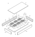
- FIG. 1 is an exploded perspective view showing an example of the configuration of a solar cell module.
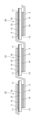
- FIG. 2 is a cross-sectional view showing an example of the structure of strings of a solar cell.
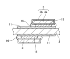
- FIG. 3 is a cross-sectional view showing a tab wire connection process according to the present technology, in which (A) shows a state in which the tab wire is placed on a conductive adhesive film, and (B) shows a state in which a metal bonding part and a covering part are formed. Indicates the condition.
- FIG. 4 is a cross-sectional view showing a solar cell to which tab wires with flat surfaces are connected.
- FIG. 5 is a cross-sectional view showing the conductive adhesive film.
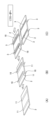
- FIG. 6 is a perspective view showing the manufacturing process of a solar cell module according to the present technology, in which (A) shows a solar cell, and (B) shows a step of attaching a conductive adhesive film to a busbar electrode and a back electrode. (C) shows the step of arranging tab wires on the conductive adhesive film.
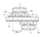
- FIG. 7 is a cross-sectional view showing a state in which the connection positions of the tab wire connected to the bus bar electrode and the tab wire connected to the back electrode are shifted by 1.0 mm from the positions where they face each other across the solar cell.
- FIG. 8 is a cross-sectional view showing a state in which the connection positions of the tab wire connected to the bus bar electrode and the tab wire connected to the back electrode are shifted by 1.0 mm from the positions where they face each other across the solar cell.
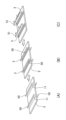
- FIG. 9 is a perspective view showing the manufacturing process of a solar cell module according to a comparative example, in which (A) shows the process of attaching the conductive adhesive film to the busbar electrode and the back electrode, and (B) shows the process of attaching the conductive adhesive film to the busbar electrode and the back electrode. The process of arranging the tab wire on top is shown, and (C) shows the process of connecting the tab wire by heating and pressing with a bonding head from above the tab wire on the bus bar electrode.
- FIG. 9 is a perspective view showing the manufacturing process of a solar cell module according to a comparative example, in which (A) shows the process of attaching the conductive adhesive film to the busbar electrode and the back electrode, and (B) shows the process of attaching the conductive adhesive film
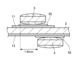
- FIG. 10 is a cross-sectional view showing a state in which the connection positions of the tab wire connected to the bus bar electrode and the tab wire connected to the back electrode are shifted by 1.0 mm from the positions where they face each other across the solar cell.
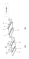
- FIG. 11 is a perspective view showing the manufacturing process of a solar cell module according to a comparative example, in which (A) shows the process of applying flux to the busbar electrode, and (B) shows the process of applying flux to the busbar electrode and the back electrode. The placement process is shown.
- FIG. 12 is a cross-sectional view showing a state in which the connection positions of the tab wire connected to the bus bar electrode and the tab wire connected to the back electrode are shifted by 1.0 mm from the positions facing each other across the solar cell.
- FIG. 11 is a perspective view showing the manufacturing process of a solar cell module according to a comparative example, in which (A) shows the process of applying flux to the busbar electrode, and (B) shows the process of applying flux to the busbar electrode and the back
- FIG. 13 is a cross-sectional view showing a state in which cracks have occurred in a solar cell in which tab wires are connected using a conductive adhesive film in which conductive particles are dispersed.
- FIG. 14 is a cross-sectional view showing a state in which cracks have occurred in a solar cell in which tab wires are connected using a conductive adhesive film in which conductive particles are dispersed.
- a solar cell module 1 to which the present invention is applied has strings 4 in which a plurality of solar cells 2 are connected in series by tab wires 3 serving as interconnectors.
- a matrix 5 is provided in which a plurality of cells 4 are arranged. Then, in the solar cell module 1, this matrix 5 is sandwiched between sheets 6 of sealing adhesive, and laminated together with a front cover 7 provided on the light-receiving surface side and a back sheet 8 provided on the back side, Finally, a metal frame 9 made of aluminum or the like is attached around the periphery.
- sealing adhesive for example, a translucent sealant such as ethylene vinyl acetate resin (EVA) is used.
- EVA ethylene vinyl acetate resin
- surface cover 7 for example, a transparent material such as glass or transparent plastic is used.
- back sheet 8 a laminate made of glass, aluminum foil sandwiched between resin films, or the like is used.
- Each solar cell 2 of the solar cell module has a photoelectric conversion element 10.
- the photoelectric conversion element 10 includes a single crystal silicon photoelectric conversion element, a crystalline silicon solar cell using a polycrystalline photoelectric conversion element, a thin film silicon solar cell made of amorphous silicon, a cell made of amorphous silicon, and a cell made of microcrystalline silicon or amorphous silicon.
- Multi-junction thin film silicon solar cells in which cells made of silicon germanium are laminated, tandem crystalline silicon solar cells in which perovskite or other organic thin film solar cells are tandemly bonded to crystalline silicon solar cells, so-called compound thin film solar cells.
- Various types of photoelectric conversion elements 10, such as , organic type, quantum dot type, etc., can be used.
- the photoelectric conversion element 10 is provided with a finger electrode 12 that collects electricity generated inside the photoelectric conversion element 10 and a busbar electrode 11 that collects electricity from the finger electrode 12 on the light receiving surface side.
- the busbar electrodes 11 and the finger electrodes 12 are formed by applying, for example, Ag paste to the light-receiving surface of the solar cell 2 by screen printing or the like, and then firing the paste.
- the finger electrodes 12 include a plurality of lines having a width of, for example, about 50 to 200 ⁇ m, which are formed substantially parallel to each other at predetermined intervals, for example, every 2 mm, over the entire surface of the light-receiving surface.
- the busbar electrodes 11 are formed to be substantially orthogonal to the finger electrodes 12, and a plurality of busbar electrodes 11 are formed depending on the area of the solar cell 2.
- the photoelectric conversion element 10 is provided with a back electrode 13 made of aluminum or silver on the back side opposite to the light receiving surface.
- the back electrode 13 is made of, for example, aluminum or silver and is formed on the back surface of the solar cell 2 by screen printing, sputtering, or the like.
- the back electrode 13 has a tab wire connection portion 14 to which the tab wire 3 is connected via a conductive adhesive such as a conductive adhesive film 18 .
- the tab wire connection portion 14 is located at a position facing the bus bar electrode 11 via the solar cell 2 body.
- each bus bar electrode 11 formed on the front surface and the back electrode 13 of the adjacent solar cell 2 are electrically connected by the tab wire 3, whereby the adjacent solar cell 2
- the strings 4 are connected in series.
- the tab wire 3, the bus bar electrode 11, and the back electrode 13 are electrically connected to each other by a conductive adhesive.
- this conductive adhesive has solder particles 20 dispersed in a thermosetting binder resin 19.
- a metal bonding portion 15 made of solder is formed at the center of the tab wire 3 in the width direction.
- the tab wire 3, the bus bar electrode 11, and the back electrode 13 are electrically and mechanically connected by a metal bonding portion 15. Further, the metal bonding portion 15 and both widthwise edges of the tab wire 3 are coated with a cured product of the binder resin 19 to form a covering portion 16 .
- the tab wire 3 is placed between the busbar electrode 11 and the back electrode 13 of the solar cell 2 via a conductive adhesive, and heated under no load or extremely low load. be done.
- the solder particles dispersed in the conductive adhesive material aggregate at approximately the center in the width direction of the tab wire 3 when heated, and connect the tab wire 3 and the bus bar electrode. 11 and the back electrode 13, a metal bonding portion 15 is formed.
- the binder resin flows outward in the width direction of the tab wire and cures while covering the metal bonding portion 15 and both widthwise edges of the tab wire 3.
- the metal bonding portion 15 is supported by the covering portion 16, and it is possible to prevent the metal bonding portion 15 from cracking, and from cracking or warping due to the difference in thermal expansion between the tab wire 3 and the solar cell 2. Furthermore, since the tab wires 3 are connected under no load or extremely low load, and the metal bonding portion 15 is supported by the covering portion 16, the arrangement of the tab wires 3 on the front and back sides of the solar cell 2 may be misaligned. In other words, the tab wire 3 connected to the light-receiving surface of the solar cell 2 and the tab wire 3 connected to the back electrode 13 are connected in a manner shifted in the width direction from positions facing each other with the solar cell 2 interposed therebetween.
- the state in which the tab wire 3 is misaligned in the width direction on the front and back surfaces of the solar cell 2 means that the tab wire 3 connected to the light-receiving surface of the solar cell 2 is connected to the back electrode 13. This refers to a state in which the tab wires 3 at least partially overlap with each other through the solar cell 2 .
- the covering portion 16 extends from both side edges of the tab wire 3 in the width direction to the side surface and covers the tab wire 3.
- the side surfaces of the tab wire 3 With the cured product of the binder resin 19, generation of cracks in the metal joint portion 15 and deformation such as waviness of the tab wire 3 can be more reliably prevented.
- the melt viscosity so that the molten binder resin 19 flows along the side edges of the tab wire 3, a situation where the molten binder resin 19 flows more than necessary onto the light receiving surface and reduces power generation efficiency is avoided. can be prevented.
- the tab wire 3 is a long conductive base material that electrically connects adjacent solar cells 2X, 2Y, and 2Z.
- the tab wire 3 is made into a rectangular shape with a width of 1 to 3 mm, for example, by slitting copper foil or aluminum foil rolled to a thickness of 50 to 300 ⁇ m, or by rolling a thin metal wire such as copper or aluminum into a flat plate.
- a wire rod 3a is obtained.
- the tab wire 3 is formed by forming a plating layer 3b of gold plating, silver plating, tin plating, solder plating, etc. on this rectangular wire 3a (see FIG. 3).
- the tab wire 3 is formed using a conductive adhesive at a position that almost overlaps on the bus bar electrode 11 formed on the light-receiving surface of the solar cell 2 and on the back electrode 13 formed on the back surface of the solar cell 2. connected by.
- the tab wire 3 connected on the bus bar electrode 11 and the tab wire 3 connected on the back electrode 13 may be misaligned by several millimeters in the width direction. In this technology, even if the tab wires 3 connected to the busbar electrode 11 and the back electrode 13 are misaligned, the connection is possible without placing an excessive load on the solar cell 2, and the solar cell It is possible to prevent cracks from occurring in the metal bonding portion 15, which is the connecting portion of the tab wire 3, and to ensure long-term conductivity reliability.
- the conductive adhesive that connects the bus bar electrode 11 and back electrode 13 of the solar cell 2 to the current collecting tab wire 3 includes a thermosetting binder resin 19 and solder particles 20 dispersed in the binder resin. .
- the conductive adhesive may be formed into a film shape as shown in FIG. 5, or may be formed into a paste shape. In the following, a conductive adhesive film 18 in which a binder resin 19 is formed into a film will be described as an example of the conductive adhesive.
- the binder resin 19 is a thermosetting binder resin, and contains solder particles 20 dispersed therein. Further, in the conductive adhesive film 18, the minimum melt viscosity of the binder resin 19 is 300 Pa ⁇ s or less, preferably 200 Pa ⁇ s or less, and more preferably 100 Pa ⁇ s or less. If the minimum melt viscosity is too high, the resin will not melt under no load or an extremely low load (for example, 10 kPa or less) in the mounting process of the tab wire 3, and the solder particles 20 will not melt between the tab wire 3 and the bus bar electrode 11. This may cause aggregation and hinder the flow of the binder resin, and the metal bonding portion 15 and the coating portion 6 may not be formed, which may adversely affect connection reliability.
- the lowest melt viscosity attainment temperature of the binder resin 19 is less than 180°C, preferably 150°C or less.
- the conductive adhesive film 16 can connect the tab wires 3 at a relatively low temperature, suppresses thermal distortion caused by the difference in thermal expansion between the tab wires and the solar cell 2, and prevents cracks, warping, etc. of the solar cell 2. can be prevented from occurring. It is preferable for the binder resin 19 to reach its minimum melt viscosity at a temperature lower than the melting point of the solder particles 20 so that the solder particles tend to aggregate with each other and to obtain a good solder connection.
- the lowest melt viscosity temperature of the conductive adhesive film 18 can be determined, for example, by using a rheometer MARS3 (manufactured by HAAKE) equipped with an 8 mm diameter sensor and plate, a gap of 0.2 mm, a heating rate of 10° C./min, and a frequency of 1 Hz.
- the melt viscosity can be determined by measuring the melt viscosity under the measurement temperature range of 20 to 250° C. and determining the temperature at which the viscosity reaches its lowest value (minimum melt viscosity).
- thermosetting binder resin 19 is not particularly limited as long as it exhibits insulation properties, and examples thereof include a thermal anionic polymerization type resin composition containing an epoxy compound and a thermal anionic polymerization initiator, and examples include a thermal cationic polymerization type resin composition containing a thermal cationic polymerization initiator, a thermal radical polymerization type resin composition containing a (meth)acrylate compound and a thermal radical polymerization initiator, and the like.
- the (meth)acrylate compound includes both acrylic monomers (oligomers) and methacrylic monomers (oligomers).
- thermally anionically polymerizable resin composition containing a film-forming resin, a solid epoxy resin, a liquid epoxy resin, and an epoxy resin curing agent will be described.
- the film-forming resin corresponds to, for example, a high molecular weight resin having an average molecular weight of 4,000 or more, and preferably has an average molecular weight of about 4,000 to 80,000 from the viewpoint of film-forming properties.
- the film-forming resin include various resins such as phenoxy resin, polyester resin, polyurethane resin, polyester urethane resin, acrylic resin, polyimide resin, butyral resin, and these may be used alone or in combination of two or more types. It may also be used. Among these, phenoxy resin is preferably used from the viewpoint of film formation state, connection reliability, and the like.
- the blending amount of the film-forming resin is preferably 10 to 60 parts by mass, more preferably 10 to 50 parts by mass or less, based on a total of 100 parts by mass of the film-forming resin, solid epoxy resin, liquid epoxy resin, and epoxy resin curing agent. , more preferably 10 to 40 parts by mass.
- the solid epoxy resin is not particularly limited as long as it is solid at room temperature and has one or more epoxy groups in the molecule; for example, bisphenol A epoxy resin, biphenyl epoxy resin, etc. There may be. Among these, it is preferable to use a crystalline bisphenol A type epoxy resin having a low melt viscosity.
- a specific example of crystalline bisphenol A type epoxy resin available on the market is "YL6810" (crystalline BPA type epoxy resin) manufactured by Mitsubishi Chemical Corporation, which has a viscosity of 40 to 55 P according to the Gardner-Holt method. etc. can be mentioned.
- the blending amount of the solid epoxy resin is preferably 10 to 60 parts by mass, more preferably 10 to 55 parts by mass or less, based on a total of 100 parts by mass of the film-forming resin, solid epoxy resin, liquid epoxy resin, and epoxy resin curing agent. , more preferably 10 to 50 parts by mass.
- normal temperature is a range of 20° C. ⁇ 15° C. (5° C. to 35° C.) defined by JIS Z 8703.
- the liquid epoxy resin is not particularly limited as long as it is liquid at room temperature, and may be, for example, a bisphenol A type epoxy resin, a bisphenol F type epoxy resin, or a urethane-modified epoxy resin. do not have. Among these, it is preferable to use a high purity hydrogenated epoxy resin. Specific examples of high-purity hydrogenated epoxy resins available on the market include "YX8000" (hydrogenated BPA type epoxy resin) manufactured by Mitsubishi Chemical Corporation.
- the amount of liquid epoxy resin blended is preferably 0 to 70 parts by mass, more preferably 5 to 65 parts by mass or less, based on a total of 100 parts by mass of the film-forming resin, solid epoxy resin, liquid epoxy resin, and epoxy resin curing agent. , more preferably 10 to 60 parts by mass.
- the epoxy resin curing agent is not particularly limited as long as it is a thermosetting agent that starts curing with heat, and examples thereof include anionic curing agents such as imidazole, dicyandiamide, and isophthalic acid dihydrazide. Moreover, the epoxy resin curing agent may be microencapsulated.
- the amount of the epoxy resin curing agent is preferably 1 to 25 parts by weight, more preferably 1 to 20 parts by weight, based on a total of 100 parts by weight of the film-forming resin, solid epoxy resin, liquid epoxy resin, and epoxy resin curing agent. The amount below is more preferably 5 to 15 parts by mass.
- thermosetting binder additives to be added to the thermosetting binder include silane coupling agents, acrylic rubber, diluent monomers such as various acrylic monomers, fillers, softeners, colorants, and flame retardants, as necessary. , a thixotropic agent, etc. may be added.
- solder particles 20 contain 40 to 80 wt% Sn and 20 to 60 wt% Bi, more preferably 42 to 75 wt% Sn and 25 to 58 wt% Bi. As a result, the molten solder aggregates at the center of the tab wire 3 in the width direction between the tab wire 3, the busbar electrode 11, and the back electrode 13 due to the conventional reflow oven treatment under normal profile conditions. A good metal bonding portion 15 can be formed between the busbar electrode 13 and the busbar electrode 13 . Further, the solder particles 20 may contain 1 wt% or less of other metals such as Cu and Ag, for example, from the viewpoint of improving solder strength.
- the melting point of the solder particles 20 is 200°C or less, preferably 185°C or less, and more preferably 175°C or less, from the viewpoint of forming a good metal bond 15 even by lowering the connection processing temperature of the tab wire 3.
- solder particles 20 for example, Sn-58Bi, Sn-40Bi-0.1Cu, Sn-30Bi-0.5Cu, Sn-20Bi, etc. can be suitably used. Among these, it is preferable to use Sn-58Bi or Sn-40Bi-0.1Cu, which has particularly excellent solder wettability.
- the lower limit of the blending amount of the solder particles 20 is preferably 200 parts by mass or more per 100 parts by mass of the binder resin 19. If the amount of solder particles 20 is less than this, there is a risk that there will be some locations where solder connection cannot be made if the tab wires 3 undulate or the solar cells warp. Further, the upper limit of the blending amount of the solder particles 20 is preferably 800 parts by mass or less per 100 parts by mass of the binder resin 19. If the blending amount of the solder particles 20 is larger than this, the tackiness when formed into a film decreases due to the relatively small amount of binder, and the conductive adhesive film 18 is temporarily attached to the busbar electrode 11 or the back electrode 13. There is a risk that poor adhesion may occur during adhesion. Furthermore, the metal bonding portion 15 may not be sufficiently covered by the covering portion 16, resulting in insufficient support.
- the lower limit of the average particle size of the solder particles 20 is preferably 5 ⁇ m or more, more preferably 10 ⁇ m or more. If the average particle size of the solder particles 20 is smaller than this, the solder particles 20 will move too much during the reflow process without a load, and will not aggregate at the center of the tab wire 3 in the width direction, resulting in a metal bond with the bus bar electrode 13. Solder particles 20 that do not contribute to the formation of portion 15 may occur. Further, the upper limit of the average particle size of the solder particles 20 is preferably 50 ⁇ m or less, more preferably 40 ⁇ m or less.
- the preferred range of the average particle size of the solder particles 20 is 5 to 20 ⁇ m.
- carboxylic acid nR-COOH
- MO metal oxides
- solder particles 20 whose surface oxide film has been reduced by the reduction reaction are caused by solder aggregation due to collisions between the solder particles 20 and contact of the solder particles 20 to the metal on the electrode surface due to the Marangoni effect or thermal flow of the binder. , it becomes possible to obtain a good connection between the electrodes.
- the above-mentioned solder particles 20 containing Sn and Bi have an appropriate amount of tin oxide on the surface, and the reaction between the tin oxide and carboxylic acid on the surface makes it easy to obtain a driving force for moving the solder particles 20. It is assumed that.
- malonic acid, succinic acid, or glutaric acid which have particularly excellent solder wettability.
- dicarboxylic acids can have not only linear structures but also branched, saturated, and unsaturated structures.
- rosin-based carboxylic acids can also be used, and dicarboxylic acids and rosin-based carboxylic acids may be used in combination. That is, it may contain a rosin-based carboxylic acid instead of the dicarboxylic acid, or may further contain a rosin-based carboxylic acid.
- the blending amount of the dicarboxylic acid is preferably 1 to 15 parts by weight, more preferably 2 to 12 parts by weight, even more preferably 4 to 10 parts by weight, and even more preferably is 6 to 10 parts by mass. If the amount of dicarboxylic acid blended is too small, the oxide film on the surface of the solder particles 20 cannot be sufficiently reduced, making it difficult to cause solder aggregation. Since the reaction also progresses more easily, the viscosity of the binder resin 19 increases, making it difficult to cause solder aggregation.
- the conductive adhesive film 18 is made by, for example, mixing a thermosetting binder resin 19, solder particles 20, and dicarboxylic acid in a solvent, and applying the mixture to a predetermined thickness on a release-treated film using a bar coater. After coating, it can be obtained by drying and volatilizing the solvent. Alternatively, the mixture may be coated onto a release-treated film using a bar coater and then applied to a predetermined thickness by applying pressure. Further, in order to improve the dispersibility of the solder particles 20, it is preferable to apply a high shear to the solder particles 20 in a state containing a solvent. For example, a known batch-type planetary stirring device can be used. It may also be possible to perform it in a vacuum environment.
- FIG. 6(A) a solar cell 2 is prepared.
- the conductive adhesive film 18 is cut into a predetermined number (for example, two) and length for the bus bar electrode 11 and the back electrode 13, and the release film is peeled off.
- FIG. 6(B) the conductive adhesive film 18 is temporarily pasted on the busbar electrode 11 on the front surface of the solar cell 2 and the tab wire connection portion 14 on the back surface of the solar cell 2 due to the tackiness of the binder resin 19. Ru. Note that when a conductive adhesive paste is used as the conductive adhesive, the conductive adhesive paste is applied onto the tab wire connection portions 14 of the busbar electrodes 11 and the back electrodes 13.
- the tab wire 3 which is similarly cut to a predetermined length, is placed in an overlapping manner on the conductive adhesive film 18.
- the tab wire 3 is placed on the bus bar electrode 11 and is also placed in an overlapping manner on the conductive adhesive film 18 temporarily attached to the back electrode 13 of the adjacent solar cell 2 .
- the tab wire 3 is connected to the busbar electrode 11 and the back electrode 13 by the conductive adhesive film 18.
- the tab wire 3 is joined to the busbar electrode 11 and the back electrode 13 using a reflow oven set to a predetermined profile, a spot hot air cell stringer, or an IR heating cell stringer.
- a reflow oven, spot hot air cell stringer, or IR heating cell stringer can be heated and bonded with no load or extremely low load without applying mechanical pressure, so it is possible to prevent waviness of the tab wire 3 and thin Damage such as cracking and warping of the solar cell 2 that has been achieved can be suppressed.
- the reflow oven atmospheric pressure reflow is preferred from the viewpoint of simplicity, but atmospheric pressure reflow, vacuum reflow, atmospheric pressure oven, autoclave (pressure oven), etc. may also be used.
- thermosetting binder resin 19 and the solder particles 20 are melted by heating.
- the molten solder aggregates at approximately the center of the tab wire 3 in the width direction, and the molten binder resin 19 flows outward of the tab wire 3 in the width direction.
- a metal bonding part 15 made of solder is formed at the center of the tab wire 3 in the width direction, and the tab wire 3 is electrically and mechanically connected to the bus bar electrode 11 and the back electrode 13. be done.
- the metal bonding portion 15 and both widthwise edges of the tab wire 3 are covered with a cured product of the binder resin 19 to form a covering portion 16 .
- the tab wire 3 may be connected by heating and pressing the tab wire 3 from above using a heating bonder.
- the pressure by the bonding head to an extremely low pressure of 50 kPa or less (for example, 10 kPa)
- the tab wires 3 can be bonded without applying any load to the solar cell 2.
- the bonding head comes into contact with the tab wire 3, it is possible to prevent the tab wire 3 from being undulated or warped.
- the tab wires 3 are connected under no load or extremely low load, and the metal bonding portion 15 is supported by the covering portion 16, so that the tab wires 3 are arranged on the front and back of the solar cell 2. Even if the metal parts 15 and 16 are misaligned, cracks will not occur in the metal bonding part 15 or the covering part 16 due to the pressure during connection. This is true regardless of whether the surface of the tab wire 3 has an arcuate shape or a flat shape when viewed in cross section.
- the solar cells 2 are successively connected by the tab wires 3 to form the strings 4 and the matrix 5.
- the plurality of solar cells 2 constituting the matrix 5 are made of a light-transmitting surface cover 7 made of glass, transparent plastic, etc., and a back sheet 8 made of glass, PET (Poly Ethylene Terephthalate) film, etc.
- a sheet 6 of a translucent sealing material such as ethylene vinyl acetate resin (EVA) is used for sealing.
- EVA ethylene vinyl acetate resin
- a metal frame 9 made of aluminum or the like is attached around the solar cell module 1 to form the solar cell module 1.
- the metal bonding portion 15 connecting the tab wire 3, the bus bar electrode 11, and the back electrode 13 is supported by the covering portion 16.
- the connection strength of the tab wire 3 can be improved, and the electrical connection between the metal bonding portion 15, the tab wire 3, and the electrodes 11 and 13 can be maintained even when exposed repeatedly to high and low temperature operating environments. It is possible to maintain high connection reliability and prevent a decrease in the output of generated electricity.
- a conductive adhesive film containing solder particles and a conductive adhesive paste containing solder particles were prepared as conductive adhesive materials, and a single cell solar panel was constructed by connecting tab wires and solar cells using the reflow method.
- a battery module was created.
- a single-cell solar cell module in which tab wire connections were made using a hot pressing method using a conductive adhesive film for tab wire connections in which conductive particles were dispersed in a thermosetting binder resin, and A single-cell solar cell module was fabricated by connecting the tab wires by a soldering method using the solder of the solder-coated tab wires as a connection material. Then, for each sample, the occurrence of cracks in the solar cell, the output retention rate at the initial stage of connection, and after the reliability test were measured and evaluated.
- solder particles Metal materials were placed in a heating container at a predetermined mixing ratio, melted, and then cooled to obtain a solder alloy. A powder was produced from the solder alloy by an atomization method, and the powder was classified to fall within a predetermined particle size range to obtain solder particles.
- Table 1 shows the melting characteristics of the solder particles used in the examples.
- Example 1 a conductive adhesive film having the following materials was produced.
- the obtained conductive resin composition was applied onto a 50 ⁇ m thick PET film to a predetermined thickness after drying, and dried at 80° C. for 5 minutes to produce a 25 ⁇ m thick conductive adhesive film.
- the minimum melt viscosity of the conductive adhesive film according to Example 1 is 50 Pa ⁇ s.
- the solar cell used was a 6-inch single-crystal silicon solar cell, two-busbar type.
- the tab wire used was a Cu foil with a width of 1.5 mm and a thickness of 200 ⁇ m plated with lead-free solder (Sn-3Ag-0.5Cu) (thickness: 20 ⁇ m on one side).
- the prepared conductive adhesive film is pasted on the tab wire connections of the busbar electrode and back electrode of the solar cell, and after the tab wires are placed, the tab wires and cell electrodes are heated and connected in a reflow oven at a maximum heating temperature of 180°C. Then, a single-cell solar cell module was fabricated (reflow method).
- Example 2 a solar cell module was produced under the same conditions as in Example 1, except that the amount of solder particles was 400 parts by mass.
- the minimum melt viscosity of the conductive adhesive film according to Example 2 is 65 Pa ⁇ s.
- Example 3 a solar cell module was produced under the same conditions as in Example 1, except that the amount of solder particles was 600 parts by mass.
- the minimum melt viscosity of the conductive adhesive film according to Example 3 is 77 Pa ⁇ s.
- Example 4 a solar cell module was produced under the same conditions as Example 1, except that the amount of solder particles was 800 parts by mass.
- the minimum melt viscosity of the conductive adhesive film according to Example 4 is 98 Pa ⁇ s.
- Example 5 a solar cell module was produced under the same conditions as Example 1, except that solder particles (Sn-40Bi-0.1Cu, average particle size: 10 ⁇ m) were used.
- the minimum melt viscosity of the conductive adhesive film according to Example 5 is 50 Pa ⁇ s.
- Example 6 a solar cell module was produced under the same conditions as Example 5, except that the amount of solder particles was 800 parts by mass.
- the minimum melt viscosity of the conductive adhesive film according to Example 6 is 98 Pa ⁇ s.
- Example 7 a conductive adhesive paste having the following materials was produced. 95 parts by mass of hydrogenated BPA epoxy (YX8000 manufactured by Mitsubishi Chemical Corporation), 5 parts by mass of imidazole (Curesol 2P4MHZ-PW manufactured by Shikoku Kasei Co., Ltd.), 1,3-propanedicarboxylic acid (glutaric acid, manufactured by Tokyo Kasei Co., Ltd.) 5 parts by mass
- solder particles Sn-40Bi-0.1Cu, average particle diameter: 10 ⁇ m
- the minimum melt viscosity of the conductive adhesive paste according to Example 7 is less than 1 Pa ⁇ s.
- Example 2 The same solar cells and tab wires as in Example 1 were used. After applying the prepared conductive adhesive paste to the tab wire connection portion 14 of the busbar electrode 11 and back electrode 13 of the solar cell and arranging the tab wire, the tab wire and cell electrode were heated at a maximum temperature of 180° C. in a reflow oven. A single-cell solar cell module was fabricated by heating and connecting the two.
- Example 8 a solar cell module was produced under the same conditions as Example 7, except that the amount of solder particles was 800 parts by mass.
- the minimum melt viscosity of the conductive adhesive paste according to Example 8 is less than 1 Pa ⁇ s.
- Comparative Example 1 used a 25 ⁇ m thick conductive adhesive film for connecting tab wires (SP103F1-25 manufactured by Dexerials) in which conductive particles (nickel, average particle size: 10 ⁇ m) were dispersed in an epoxy thermosetting binder resin. . The same solar cells and tab wires as in Example 1 were used.
- this anisotropic conductive film 50 is temporarily attached to the tab wire connection portions of the busbar electrode 11 and back electrode 13 of the solar cell 2 (FIG. 9(A)), and the anisotropic conductive film After placing the tab wire 3 on the bus bar electrode 11 (FIG. 9(B)), the tab wire 3 on the bus bar electrode 11 is connected by heating and pressing with the bonding head 51 (FIG. 9(C)).
- a solar cell module was fabricated using the heat pressing method. The heat and pressure conditions of the bonding head 51 were 180° C., 3 MPa, and 20 seconds.
- Comparative example 2 In Comparative Example 2, a Cu foil with a width of 1.5 mm and a thickness of 200 ⁇ m plated with lead-free solder (Sn-58Bi) was used as the tab wire (thickness: 20 ⁇ m on one side). Furthermore, the connection was made using solder provided on the surface of the tab wire without using a conductive adhesive. The same solar cells and tab wires as in Example 1 were used.
- a flux 52 is applied to the busbar electrode 11 and the back electrode 13 (FIG. 11(A)), and then the tab wire 3 is placed on the busbar electrode 11 and the back electrode 13. (FIG. 11(B)), the tab wire 3, busbar electrode 11, and back electrode 13 were heated and connected in a reflow oven at a maximum heating temperature of 180° C. to produce a single-cell solar cell module (soldering method).
- the samples according to Examples 7 and 8 no cracks were observed in the solar cells.
- the output retention rate after the temperature cycle test was 97% or more, indicating that it had continuity reliability over a long period of time.
- Comparative Example 1 in which the tab wires were connected using a conductive adhesive film containing nickel particles by a hot pressing method, large cracks appeared in the solar cell after the tab wires were crimped, and immediately after lamination, It was not possible to obtain cell output characteristics. Therefore, it was excluded from the temperature cycle test. This is thought to be because a pressure of 3 MPa was applied with the front and back tab lines misaligned, and the solar cell was cracked due to shear stress.
- Comparative Example 2 which was reflow mounted using only solder (Sn-58Bi) provided on the surface of the tab wire, although no cracks occurred, a significant decrease in output was observed after the temperature cycle test. At the connection site between the solar cell and the tab wire, it was confirmed that the tab wire was peeling off from the end, which is thought to be due to the brittle characteristics of the Bi eutectic solder.
Landscapes
- Photovoltaic Devices (AREA)
Abstract
太陽電池セルの表裏におけるタブ線の位置ズレが生じたとしても、太陽電池セルの割れや反り、タブ線との接続部におけるクラックの発生を防止する。 太陽電池モジュール1は、太陽電池セル2と、太陽電池セル2の表裏に形成された電極11,13と接続されたタブ線3を有し、タブ線3の幅方向の中央部に、タブ線3と電極11,13を接続するはんだによる金属結合部15が形成され、熱硬化性のバインダー樹脂の硬化物からなり、断面視において、金属結合部15、及びタブ線3の両側縁を被覆する被覆部16を有する。
Description
本技術は、太陽電池モジュール、太陽電池セルとタブ線を接続する導電性接着材、及び太陽電池モジュールの製造方法に関する。本出願は、日本国において2022年7月5日に出願された日本特許出願番号特願2022-108510を基礎として優先権を主張するものであり、この出願は参照されることにより、本出願に援用される。
従来、太陽電池モジュール内の太陽電池セルと、太陽電池セルで発電した電気を取り出す集電用のタブ線とを接続する方法として、はんだ接続工法が用いられている。タブ線は、銅線をはんだで被覆した線材であり、太陽電池セルに設けられた集電電極(バスバー電極)上に配置した後、ボンディングヘッドによりはんだ接続温度以上の温度で加熱押圧することにより接合を行っている。
タブ線の接続温度は、被覆はんだとして、一般的な鉛フリー共晶はんだのSn-3Ag-0.5Cu系を使用した場合、250℃程度と高温となる。シリコン系太陽電池セルの原料となるシリコンは、比較的熱膨張が小さい材料であるのに対して、タブ線に使用される銅は熱膨張が大きく、この熱膨張差からタブ線の接続時に熱ひずみが発生する。接続温度が高いほどこのひずみは大きくなるため、太陽電池セルのタブ線が接続された部位に割れや反りが発生するおそれがある。
また、銅線を被覆するはんだ材料として、低温共晶はんだのSn-58Bi系を用いると、Bi共晶はんだの脆い特性からタブ線と太陽電池セルの線膨張差によってはんだ接続部にクラックが発生し、また長期にわたって導通信頼性を確保することが困難となる。
そこで、従来のはんだ接続工法に代わり、導電性接着材を用いる工法が提案されている(特許文献1)。導電性接着材は、フィルム状に加工した硬化性樹脂組成物内に導電粒子が分散された接合材料であり、太陽電池セルのバスバー電極上に貼付し、タブ線とともに熱加圧することによりタブ線とバスバー電極を導通接続する。この工法では、上述したはんだ接続工法よりも低温で加熱押圧することで太陽電池セルとタブ線を接続することが可能となり、はんだ接続工法に対して優位性がある。
しかし、導電性接着材を用いた工法は、タブ線の接続時に数MPa程度の圧力をかける必要が有る。一般的に使用されているタブ線は、溶解したはんだに銅線を浸漬してはんだ付けを行うディップメッキ加工が施されており、図13に示すように、断面視において被覆はんだ103により中央部が膨らんだ形状を有する。このため、太陽電池セル101の表裏においてタブ線102の位置ずれが発生すると、接続時の圧力によりタブ線102の接続部104にクラックが発生したり、太陽電池セル101のタブ線102が接続された部位に割れや反りが発生したりするおそれがある。
また、図14に示すような断面視において平坦な形状を有するタブ線102を用いた場合でも、太陽電池セル101の表裏におけるタブ線102の位置が大きくずれると、同様にクラックや割れ等が発生するおそれがあった。
そこで、本技術は、太陽電池セルの表裏におけるタブ線の位置ズレが生じたとしても、太陽電池セルの割れや反り、タブ線との接続部におけるクラックの発生を防止し、且つ長期にわたる導通性信頼性を確保できる太陽電池モジュール及び接続材料を提供することを目的とする。
上述した課題を解決するために、本技術に係る太陽電池モジュールは、太陽電池セルと、上記太陽電池セルの表裏に形成された電極と接続されたタブ線を有し、上記タブ線の幅方向の中央部に、上記タブ線と上記電極を接続するはんだによる金属結合部が形成され、熱硬化性のバインダー樹脂の硬化物からなり、断面視において、上記金属結合部、及びタブ線の両側縁を被覆する被覆部を有するものである。
また、本技術に係る導電性接着材は、複数の太陽電池セルが直列に接続されてなる太陽電池モジュールの少なくとも一つの太陽電池セルの集電電極を集電用タブ線と接続するための導電性接着剤において、熱硬化型エポキシ樹脂とイミダゾール系潜在性硬化剤とを含有するバインダー樹脂と、上記バインダー樹脂中に分散されたはんだ粒子を有し、上記はんだ粒子は、Bi系のはんだ粒子である。
また、本技術に係る太陽電池モジュールの製造方法は、太陽電池セルの電極上に熱硬化型の導電性接着材を設ける工程と、上記導電性接着材の上に集電用のタブ線を配置する工程と、上記太陽電池を加熱し、上記タブ線を50kPa以下の荷重又は無荷重で実装する工程を有し、上記導電性接着材は、上記記載の導電性接着材であり、上記タブ線の幅方向の中央部に、はんだによる金属結合部が形成され、熱硬化性のバインダー樹脂の硬化物からなり、断面視において、上記金属結合部、及びタブ線の両側縁を被覆する被覆部を有するものである。
本技術によれば、金属結合部が被覆部によってサポートされることにより、金属結合部のクラックの発生や、タブ線との熱膨張差等による太陽電池セルの割れや反りを防止することができる。
以下、本技術が適用された太陽電池モジュール、導電性接着材、及び太陽電池モジュールの製造方法について、図面を参照しながら詳細に説明する。なお、本技術は、以下の実施形態のみに限定されるものではなく、本技術の要旨を逸脱しない範囲内において種々の変更が可能であることは勿論である。また、図面は模式的なものであり、各寸法の比率等は現実のものとは異なることがある。具体的な寸法等は以下の説明を参酌して判断すべきものである。また、図面相互間においても互いの寸法の関係や比率が異なる部分が含まれていることは勿論である。
本発明が適用された太陽電池モジュール1は、図1、図2に示すように、複数の太陽電池セル2がインターコネクタとなるタブ線3によって直列に接続されたストリングス4を有し、このストリングス4を複数配列したマトリクス5を備える。そして、太陽電池モジュール1は、このマトリクス5が封止接着剤のシート6で挟まれ、受光面側に設けられた表面カバー7及び裏面側に設けられたバックシート8とともに一括してラミネートされ、最後に、周囲にアルミニウムなどの金属フレーム9が取り付けられることにより形成される。
封止接着剤としては、例えばエチレンビニルアセテート樹脂(EVA)等の透光性封止材が用いられる。また、表面カバー7としては、例えば、ガラスや透光性プラスチック等の透光性の材料が用いられる。また、バックシート8としては、ガラスや、アルミニウム箔を樹脂フィルムで挟持した積層体等が用いられる。
太陽電池モジュールの各太陽電池セル2は、光電変換素子10を有する。光電変換素子10は、単結晶型シリコン光電変換素子、多結晶型光電変換素子を用いる結晶シリコン系太陽電池や、アモルファスシリコンからなる薄膜シリコン系太陽電池、アモルファスシリコンからなるセルと微結晶シリコンやアモルファスシリコンゲルマニウムからなるセルとを積層させた多接合型の薄膜シリコン系太陽電池、結晶シリコン太陽電池にペロブスカイト型等の有機薄膜太陽電池をタンデム結合させたタンデム結晶シリコン太陽電池、いわゆる化合物薄膜系太陽電池、有機系、量子ドット型など、各種光電変換素子10を用いることができる。
また、光電変換素子10は、受光面側に内部で発生した電気を集電するフィンガー電極12とフィンガー電極12の電気を集電するバスバー電極11とが設けられている。バスバー電極11及びフィンガー電極12は、太陽電池セル2の受光面となる表面に、例えばAgペーストがスクリーン印刷等により塗布された後、焼成されることにより形成される。また、フィンガー電極12は、受光面の全面に亘って、例えば約50~200μm程度の幅を有するラインが、所定間隔、例えば2mmおきに、ほぼ平行に複数形成されている。バスバー電極11は、フィンガー電極12と略直交するように形成され、また、太陽電池セル2の面積に応じて複数形成されている。
また、光電変換素子10は、受光面と反対の裏面側に、アルミニウムや銀からなる裏面電極13が設けられている。裏面電極13は、図2に示すように、例えばアルミニウムや銀からなる電極が、スクリーン印刷やスパッタ等により太陽電池セル2の裏面に形成される。裏面電極13は、導電性接着フィルム18等の導電性接着材を介してタブ線3が接続されるタブ線接続部14を有する。タブ線接続部14は、バスバー電極11と太陽電池セル2本体を介して向かい合う位置とされる。
そして、太陽電池セル2は、タブ線3によって、表面に形成された各バスバー電極11と、隣接する太陽電池セル2の裏面電極13とが電気的に接続され、これにより隣接する太陽電池セル2と直列に接続されたストリングス4を構成する。
[金属結合部・被覆部]
タブ線3とバスバー電極11及び裏面電極13とは、導電性接着材によって導電接続される。図3(A)に示すように、この導電性接着材は、熱硬化性のバインダー樹脂19中にはんだ粒子20が分散されたものである。図3(B)に示すように、タブ線3の幅方向の中央部には、はんだによる金属結合部15が形成される。タブ線3とバスバー電極11及び裏面電極13とは、金属結合部15によって電気的、機械的に接続される。また、金属結合部15、及びタブ線3の幅方向の両側縁は、バインダー樹脂19の硬化物によって被覆されることにより被覆部16が形成されている。
タブ線3とバスバー電極11及び裏面電極13とは、導電性接着材によって導電接続される。図3(A)に示すように、この導電性接着材は、熱硬化性のバインダー樹脂19中にはんだ粒子20が分散されたものである。図3(B)に示すように、タブ線3の幅方向の中央部には、はんだによる金属結合部15が形成される。タブ線3とバスバー電極11及び裏面電極13とは、金属結合部15によって電気的、機械的に接続される。また、金属結合部15、及びタブ線3の幅方向の両側縁は、バインダー樹脂19の硬化物によって被覆されることにより被覆部16が形成されている。
図3(A)に示すように、タブ線3は、太陽電池セル2のバスバー電極11や裏面電極13との間に導電性接着材を介して配置され、無荷重あるいは極低荷重下で加熱される。これにより、図3(B)に示すように、導電性接着材中に分散されたはんだ粒子は、加熱されるとタブ線3の幅方向の略中央部に凝集し、タブ線3とバスバー電極11や裏面電極13との間に金属結合部15を形成する。バインダー樹脂は、タブ線の幅方向の外側に流動し、金属結合部15、及びタブ線3の幅方向の両側縁を被覆した状態で硬化する。
これにより、金属結合部15が被覆部16によってサポートされ、金属結合部15のクラックの発生や、タブ線3と太陽電池セル2との熱膨張差等による割れや反りを防止することができる。また、タブ線3が、無荷重あるいは極低荷重下で接続され、且つ金属結合部15が被覆部16によってサポートされているため、太陽電池セル2の表裏においてタブ線3の配置がずれていても、すなわち、太陽電池セル2の受光面に接続されたタブ線3と裏面電極13に接続されたタブ線3が、太陽電池セル2を介して向かい合う位置から幅方向にズレて接続されていても、接続時の圧力に起因して金属結合部15にクラックが生じたり、太陽電池セル2に割れや反りが発生したりするといったこともない。これは、断面視において、図3(B)に示すようにタブ線3の表面が円弧状に膨らんだ形状を有しているか、図4に示すように平坦な形状を有しているかを問わない。なお、本技術において、タブ線3が太陽電池セル2の表裏面において幅方向にズレている状態とは、太陽電池セル2の受光面に接続されたタブ線3と裏面電極13に接続されたタブ線3が、太陽電池セル2を介して少なくとも一部が重畳する状態をいうものとする。
被覆部16は、タブ線3の幅方向の両側縁から側面まで這い上がって被覆することが好ましい。タブ線3の側面までバインダー樹脂19の硬化物で覆われることで、より確実に金属結合部15のクラックの発生や、タブ線3のうねり等の変形を防止することができる。なお、溶融したバインダー樹脂19がタブ線3の側縁に沿って流動するように、溶融粘度を調整することで、溶融したバインダー樹脂19が受光面に必要以上に流れて発電効率を低下させる事態を防止することができる。
[タブ線]
タブ線3は、図2に示すように、隣接する太陽電池セル2X、2Y、2Zの各間を電気的に接続する長尺状の導電性基材である。タブ線3は、例えば厚さ50~300μmに圧延された銅箔やアルミ箔をスリットし、あるいは銅やアルミなどの細い金属ワイヤーを平板状に圧延することにより、例えば1~3mm幅の平角の線材3aを得る。そして、この平角線材3aに、金メッキ、銀メッキ、スズメッキ、はんだメッキ等によるメッキ層3bが形成されることにより、タブ線3が形成される(図3参照)。
タブ線3は、図2に示すように、隣接する太陽電池セル2X、2Y、2Zの各間を電気的に接続する長尺状の導電性基材である。タブ線3は、例えば厚さ50~300μmに圧延された銅箔やアルミ箔をスリットし、あるいは銅やアルミなどの細い金属ワイヤーを平板状に圧延することにより、例えば1~3mm幅の平角の線材3aを得る。そして、この平角線材3aに、金メッキ、銀メッキ、スズメッキ、はんだメッキ等によるメッキ層3bが形成されることにより、タブ線3が形成される(図3参照)。
ここで、タブ線3は、太陽電池セル2の受光面に形成されたバスバー電極11上、及び太陽電セル2の裏面に形成された裏面電極13上の、ほぼ重畳する位置に導電性接着材によって接続される。バスバー電極11上に接続されたタブ線3と、裏面電極13上に接続されたタブ線3とは、幅方向に数mm程度のずれが生じ得る。本技術においては、バスバー電極11上及び裏面電極13上に接続されたタブ線3に位置ずれが生じたとしても、太陽電池セル2に過剰な負荷をかけることなく接続可能であり、太陽電池セル2の割れや反り、タブ線3の接続部位である金属結合部15のクラックの発生を防止し、且つ長期にわたる導通性信頼性を確保できる。
[導電性接着材]
太陽電池セル2のバスバー電極11や裏面電極13と集電用のタブ線3を接続する導電性接着材は、熱硬化性のバインダー樹脂19と、バインダー樹脂中に分散されたはんだ粒子20を有する。導電性接着材は、図5に示すようにフィルム状に形成してもよく、ペースト状に形成してもよい。以下では、導電性接着材として、バインダー樹脂19をフィルム状に成形した導電性接着フィルム18を例に説明する。
太陽電池セル2のバスバー電極11や裏面電極13と集電用のタブ線3を接続する導電性接着材は、熱硬化性のバインダー樹脂19と、バインダー樹脂中に分散されたはんだ粒子20を有する。導電性接着材は、図5に示すようにフィルム状に形成してもよく、ペースト状に形成してもよい。以下では、導電性接着材として、バインダー樹脂19をフィルム状に成形した導電性接着フィルム18を例に説明する。
バインダー樹脂19は、熱硬化性のバインダー樹脂であり、はんだ粒子20が分散して含有されている。また、導電性接着フィルム18は、バインダー樹脂19の最低溶融粘度が、300Pa・s以下であり、好ましくは200Pa・s以下、より好ましくは100Pa・s以下である。最低溶融粘度が高すぎると、タブ線3の実装工程において、無荷重あるいは極低荷重(例えば10kPa以下)下で樹脂溶融が進行せず、タブ線3とバスバー電極11間でのはんだ粒子20の凝集やバインダー樹脂の流動に支障を来し、金属結合部15及び被覆部6が形成できず接続信頼性に悪影響が出るおそれがある。
バインダー樹脂19の最低溶融粘度到達温度は、180℃未満であり、好ましくは150℃以下である。導電接着フィルム16は、比較的低温でタブ線3を接続することができ、タブ線と太陽電池セル2との熱膨張差に起因する熱ひずみを抑制し、太陽電池セル2の割れや反り等の発生を防止することができる。バインダー樹脂19は、はんだ粒子20の融点よりも低い温度で最低溶融粘度に到達していることが、はんだ同士が凝集しやすく、良好なはんだ接続を得るうえで好ましい。
なお、導電性接着フィルム18の最低溶融粘度到達温度は、例えば、レオメーターMARS3(HAAKE社製)に8mm径センサーとプレートを装着し、ギャップ0.2mm、昇温速度10℃/min、周波数1Hz、測定温度範囲20~250℃の条件にて溶融粘度を測定し、粘度が最低値(最低溶融粘度)となる温度により求めることができる。
熱硬化性のバインダー樹脂19としては、絶縁性を示すものであれば特に限定されるものではなく、例えば、エポキシ化合物と熱アニオン重合開始剤とを含む熱アニオン重合型樹脂組成物、エポキシ化合物と熱カチオン重合開始剤とを含む熱カチオン重合型樹脂組成物、(メタ)アクリレート化合物と熱ラジカル重合開始剤とを含む熱ラジカル重合型樹脂組成物などが挙げられる。なお、(メタ)アクリレート化合物とは、アクリルモノマー(オリゴマー)、及びメタクリルモノマー(オリゴマー)のいずれも含む意味である。
以下では、具体例として、膜形成樹脂と、固形エポキシ樹脂と、液状エポキシ樹脂と、エポキシ樹脂硬化剤とを含有する熱アニオン重合型樹脂組成物を例に挙げて説明する。
膜形成樹脂としては、例えば平均分子量が4000以上の高分子量樹脂に相当し、フィルム形成性の観点から、4000~80000程度の平均分子量であることが好ましい。膜形成樹脂としては、フェノキシ樹脂、ポリエステル樹脂、ポリウレタン樹脂、ポリエステルウレタン樹脂、アクリル樹脂、ポリイミド樹脂、ブチラール樹脂等の種々の樹脂が挙げられ、これらは単独で用いてもよく、2種類以上を組み合わせて用いてもよい。これらの中でも、膜形成状態、接続信頼性等の観点からフェノキシ樹脂を用いることが好ましい。膜形成樹脂の配合量は、膜形成樹脂、固形エポキシ樹脂、液状エポキシ樹脂、及びエポキシ樹脂硬化剤の合計100質量部に対し、好ましくは10~60質量部、より好ましくは10~50質量部以下、さらに好ましくは10~40質量部である。
固形エポキシ樹脂は、常温で固形であり、分子内に1つ以上のエポキシ基を有するエポキシ樹脂であれば、特に限定されるものではなく、例えば、ビスフェノールA型エポキシ樹脂、ビフェニル型エポキシ樹脂等であってもよい。これらの中でも、低溶融粘度である結晶性のビスフェノールA型エポキシ樹脂を用いることが好ましい。市場で入手可能な結晶性のビスフェノールA型エポキシ樹脂の具体例としては、ガードナー・ホルト法の粘度が40~55Pである三菱ケミカル(株)の商品名「YL6810」(結晶性BPA型エポキシ樹脂)等を挙げることができる。固形エポキシ樹脂の配合量は、膜形成樹脂、固形エポキシ樹脂、液状エポキシ樹脂、及びエポキシ樹脂硬化剤の合計100質量部に対し、好ましくは10~60質量部、より好ましくは10~55質量部以下、さらに好ましくは10~50質量部である。なお、本明細書において常温とは、JIS Z 8703で規定する20℃±15℃(5℃~35℃)の範囲である。
液状エポキシ樹脂は、常温で液状であれば、特に限定されるものではなく、例えば、ビスフェノールA型エポキシ樹脂、ビスフェノールF型エポキシ樹脂等であってもよく、ウレタン変性のエポキシ樹脂であっても構わない。これらの中でも、高純度水添エポキシ樹脂を用いることが好ましい。市場で入手可能な高純度水添エポキシ樹脂の具体例としては、三菱ケミカル(株)の商品名「YX8000」(水添BPA型エポキシ樹脂)等を挙げることができる。液状エポキシ樹脂の配合量は、膜形成樹脂、固形エポキシ樹脂、液状エポキシ樹脂、及びエポキシ樹脂硬化剤の合計100質量部に対し、好ましくは0~70質量部、より好ましくは5~65質量部以下、さらに好ましくは10~60質量部である。
エポキシ樹脂硬化剤は、熱で硬化が開始する熱硬化剤であれば、特に限定されるものではなく、例えば、イミダゾール、ジシアンジアミド、イソフタル酸ジヒドラジド等のアニオン系硬化剤が挙げられる。また、エポキシ樹脂硬化剤は、マイクロカプセル化されていてもよい。エポキシ樹脂硬化剤の配合量は、膜形成樹脂、固形エポキシ樹脂、液状エポキシ樹脂、及びエポキシ樹脂硬化剤の合計100質量部に対し、好ましくは1~25質量部、より好ましくは1~20質量部以下、さらに好ましくは5~15質量部である。
なお、熱硬化性バインダーに配合する他の添加物として、必要に応じて、シランカップリング剤、アクリルゴム、各種アクリルモノマー等の希釈用モノマー、充填剤、軟化剤、着色剤、難燃化剤、チキソトロピック剤等を配合してもよい。
[はんだ粒子]
はんだ粒子20は、40~80wt%のSnと、20~60wt%のBiとを含み、より好ましくは42~75wt%のSnと、25~58wt%のBiとを含む。これにより、従来の通常のプロファイル条件のリフロー炉処理により、タブ線3とバスバー電極11及び裏面電極13との間において、溶融はんだがタブ線3の幅方向中央部に凝集し、タブ線3とバスバー電極13との間に良好な金属結合部15を形成することができる。また、はんだ粒子20は、例えばはんだ強度向上の観点から、1Wt%以下のCu、Agなどの他の金属を含んでいてもよい。
はんだ粒子20は、40~80wt%のSnと、20~60wt%のBiとを含み、より好ましくは42~75wt%のSnと、25~58wt%のBiとを含む。これにより、従来の通常のプロファイル条件のリフロー炉処理により、タブ線3とバスバー電極11及び裏面電極13との間において、溶融はんだがタブ線3の幅方向中央部に凝集し、タブ線3とバスバー電極13との間に良好な金属結合部15を形成することができる。また、はんだ粒子20は、例えばはんだ強度向上の観点から、1Wt%以下のCu、Agなどの他の金属を含んでいてもよい。
はんだ粒子20の融点は、タブ線3の接続処理温度の低温化によっても良好な金属結合部15を形成する観点から、200℃以下、好ましくは185℃以下であり、175℃以下がさらに好ましい。
このようなはんだ粒子20としては、例えばSn-58Bi、Sn-40Bi-0.1Cu、Sn-30Bi-0.5Cu、Sn-20Biなどを好適に用いることができる。これらの中でも、はんだ濡れ性が特に優れるSn-58Bi又はSn-40Bi-0.1Cuを用いることが好ましい。
はんだ粒子20の配合量の下限は、バインダー樹脂19が100質量部に対して200質量部以上とすることが好ましい。はんだ粒子20の配合量がこれよりも少なくなると、タブ線3のうねりや太陽電池セルの反りが生じた場合にはんだ接続ができない個所が出るおそれがある。また、はんだ粒子20の配合量の上限は、バインダー樹脂19が100質量部に対して800質量部以下とすることが好ましい。はんだ粒子20の配合量がこれよりも多くなると、相対的にバインダー量が少なくなることでフィルム化した際のタック性が減少し、導電性接着フィルム18をバスバー電極11や裏面電極13上に仮貼りする際に貼付け不良等が生じるおそれがある。また、被覆部16によって金属結合部15を十分に被覆することができずサポートが不十分となる恐れがある。
はんだ粒子20の平均粒径の下限は、好ましくは5μm以上、より好ましくは10μm以上である。はんだ粒子20の平均粒径がこれよりも小さ過ぎると、無荷重でのリフロー処理時にはんだ粒子20が動き過ぎて、タブ線3の幅方向中央部に凝集せず、バスバー電極13との金属結合部15の形成に寄与しないはんだ粒子20が生じ得る。また、はんだ粒子20の平均粒径の上限は、好ましくは50μm以下、より好ましくは40μm以下である。はんだ粒子20の平均粒径がこれよりも大き過ぎても、はんだ粒子20の動きが悪くなり、タブ線3の幅方向中央部に凝集せず、良好な金属結合部15を形成することが困難となる。このような観点から、はんだ粒子20の平均粒径の好ましい範囲は、5~20μmである。
[ジカルボン酸]
なお、はんだ粒子20の表面の酸化膜を還元し、酸化膜の量を減少させて、はんだ粒子20を凝集させるために下記式(1)で示されるジカルボン酸を配合しても良い(n=1~8)。
なお、はんだ粒子20の表面の酸化膜を還元し、酸化膜の量を減少させて、はんだ粒子20を凝集させるために下記式(1)で示されるジカルボン酸を配合しても良い(n=1~8)。

また、カルボン酸(nR-COOH)は、下記式(2)で示される還元反応によって金属酸化物(MO)を減少させることが知られている。

還元反応によって表面の酸化膜が減少したはんだ粒子20は、マランゴニ効果やバインダーの熱流動によって、はんだ粒子20同士の衝突や電極表面の金属へのはんだ粒子20の接触によるはんだ凝集が発生することにより、電極間の良好な接続を得ることが可能になる。SnとBiを含む上述したはんだ粒子20は、表面の酸化スズの量が適量であり、表面の酸化スズとカルボン酸とが反応することにより、はんだ粒子20が移動する駆動力が得られ易いものと推測される。
すなわち、ジカルボン酸として、マロン酸(n=1、炭素数3)、コハク酸(n=2、炭素数4)、グルタル酸(n=3、炭素数5)、アジピン酸(n=4、炭素数6)、ピメリン酸(n=5、炭素数7)、スベリン酸(n=6、炭素数8)、アゼライン酸(n=7、炭素数9)、セバシン酸(n=8、炭素数10)を用いることが好ましい。これらの中でも、はんだ濡れ性が特に優れるマロン酸、コハク酸、又はグルタル酸を用いることが好ましい。また、ジカルボン酸は直鎖だけではなく分岐、飽和、不飽和構造も使用することが出来る。また、ジカルボン酸以外に、ロジン系のカルボン酸も使用することができ、ジカルボン酸とロジン系カルボン酸を組み合わせて使用しても良い。すなわち、ジカルボン酸の代わりにロジン系のカルボン酸を含有する、又は、ロジン系カルボン酸をさらに含有してもよい。
ジカルボン酸の配合量は、熱硬化性のバインダー樹脂19が100質量部に対し、好ましくは1~15質量部、より好ましくは2~12質量部、さらに好ましくは4~10質量部、よりさらに好ましくは6~10質量部である。ジカルボン酸の配合量が少な過ぎると、はんだ粒子20の表面の酸化膜の還元が十分に行えず、はんだ凝集を発生させることが困難となり、ジカルボン酸の配合量が多過ぎると、エポキシ樹脂との反応も進みやすくなるため、それによってバインダー樹脂19の粘度が上がり、はんだ凝集を発生させ難くなる。
導電性接着フィルム18は、例えば、熱硬化性のバインダー樹脂19、はんだ粒子20、及びジカルボン酸を溶剤中で混合し、この混合物を、バーコーターにより、剥離処理フィルム上に所定厚みとなるように塗布した後、乾燥させて溶媒を揮発させることにより得ることができる。また、混合物をバーコーターにより剥離処理フィルム上に塗布した後、加圧により所定厚みとしてもよい。また、はんだ粒子20の分散性を高くするために、溶媒を含んだ状態で高シェアをかけることが好ましい。例えば、公知のバッチ式遊星攪拌装置を用いることができる。真空環境下で行えるものであってもよい。
[太陽電池モジュールの製造工程(タブ線の接続工程)]
次いで、タブ線3の接続工程について説明する。図6(A)に示すように、太陽電池セル2が用意される。導電性接着フィルム18は、バスバー電極11用及び裏面電極13用を所定の本数(例えば2本)及び長さにカットされ、剥離フィルムが剥離される。図6(B)に示すように、導電性接着フィルム18は、バインダー樹脂19のタック性によって太陽電池セル2表面のバスバー電極11上及び太陽電池セル2裏面のタブ線接続部14に仮貼りされる。なお、導電性接着材として導電性接着ペーストを用いる場合は、バスバー電極11及び裏面電極13のタブ線接続部14上に導電性接着ペーストが塗布される。
次いで、タブ線3の接続工程について説明する。図6(A)に示すように、太陽電池セル2が用意される。導電性接着フィルム18は、バスバー電極11用及び裏面電極13用を所定の本数(例えば2本)及び長さにカットされ、剥離フィルムが剥離される。図6(B)に示すように、導電性接着フィルム18は、バインダー樹脂19のタック性によって太陽電池セル2表面のバスバー電極11上及び太陽電池セル2裏面のタブ線接続部14に仮貼りされる。なお、導電性接着材として導電性接着ペーストを用いる場合は、バスバー電極11及び裏面電極13のタブ線接続部14上に導電性接着ペーストが塗布される。
次いで、図6(C)に示すように、同様に所定の長さにカットされたタブ線3が導電性接着フィルム18上に重畳配置される。タブ線3はバスバー電極11上に配置されるとともに、隣接する太陽電池セル2の裏面電極13に仮貼りされた導電性接着フィルム18上に重畳配置される。次いで、太陽電池セル2が加熱されることにより、タブ線3は導電性接着フィルム18によってバスバー電極11及び裏面電極13と接続される。タブ線3の接続工程では、所定のプロファイルに設定されたリフロー炉、スポット熱風のセルストリンガー、またはIR加熱のセルストリンガーを用いて、タブ線3とバスバー電極11及び裏面電極13とを接合させる。
リフロー炉、スポット熱風のセルストリンガー、またはIR加熱のセルストリンガーは、機械的な加圧をせずに無荷重、もしくは極低荷重で加熱接合させることができるため、タブ線3のうねりや、薄型化が図られた太陽電池セル2の割れや反り等のダメージを抑制することができる。リフロー炉としては、簡便さの点から大気圧リフローが好ましいが、大気圧リフロー、真空リフロー、大気圧オーブン、オートクレーブ(加圧オーブン)などを用いても良い。
リフロー炉、スポット熱風のセルストリンガー、またはIR加熱のセルストリンガーでは、加熱により熱硬化性のバインダー樹脂19が溶融するとともに、はんだ粒子20が溶融する。タブ線3とバスバー電極11との間では、溶融したはんだがタブ線3の幅方向の略中央部に凝集するとともに、溶融したバインダー樹脂19がタブ線3の幅方向の外側に流動する。この状態で冷却することにより、タブ線3の幅方向の中央部には、はんだによる金属結合部15が形成され、タブ線3とバスバー電極11及び裏面電極13とが電気的、機械的に接続される。また、金属結合部15、及びタブ線3の幅方向の両側縁は、バインダー樹脂19の硬化物によって被覆されることにより被覆部16が形成される。
なお、タブ線3の接続は、加熱ボンダーを用いてタブ線3の上から加熱押圧することにより行ってもよい。この場合、ボンディングヘッドによる圧力は50kPa以下の極低圧(例えば10kPa)程度とすることで、太陽電池セル2への負荷をかけることなくタブ線3を接合することができる。また、タブ線3にボンディングヘッドが当接することで、タブ線3にうねりや反りが生じることを防止できる。
また、本技術においては、タブ線3が無荷重あるいは極低荷重下で接続され、且つ金属結合部15が被覆部16によってサポートされているため、太陽電池セル2の表裏においてタブ線3の配置がずれていても、接続時の圧力に起因して金属結合部15や被覆部16にクラックが生じるといったこともない。これは、断面視において、タブ線3の表面が円弧状に膨らんだ形状を有しているか、平坦な形状を有しているかを問わない。
このようにして、太陽電池セル2を順次タブ線3によって接続し、ストリングス4、マトリクス5を形成していく。次いで、マトリクス5を構成する複数の太陽電池セル2は、ガラス、透光性プラスチックなどの透光性を有する表面カバー7と、ガラスやPET(Poly Ethylene Terephthalate)フィルム等からなるバックシート8との間に、エチレンビニルアセテート樹脂(EVA)等の透光性を有する封止材のシート6により封止される。最後に、周囲にアルミニウムなどの金属フレーム9が取り付けられることにより太陽電池モジュール1が形成される。
このような太陽電池モジュール1は、タブ線3とバスバー電極11及び裏面電極13とを接続する金属結合部15が被覆部16によってサポートされている。これにより、太陽電池セル2の割れや反り、接続部位のクラックの発生が長期わたって抑制される。したがって、タブ線3の接続強度を向上させることができ、また、高温と低温の使用環境下に繰り返し曝された場合にも、金属結合部15とタブ線3及び電極11,13との電気的な接続信頼性を維持し、発電した電気の出力低下を防止することができる。
次いで、本技術の実施例について説明する。本実施例では、導電性接着材として、はんだ粒子を含有した導電性接着フィルム及びはんだ粒子を含有した導電性接着ペーストを用意し、リフロー工法によりタブ線と太陽電池セルを接続した単セルの太陽電池モジュールを作製した。また、比較例として、熱硬化性バインダー樹脂に導電粒子を分散したタブ線接続用の導電性接着フィルムを用いて熱加圧工法によりタブ線接続を行った単セルの太陽電池モジュール、及び表面がはんだ被覆されたタブ線の当該はんだを接続材料としてはんだ工法によりタブ線接続を行った単セルの太陽電池モジュールを作製した。そして、各サンプルについて、太陽電池セルのクラック発生、接続初期及び信頼性試験後の出力保持率を測定、評価した。
[はんだ粒子の作製]
金属材料を所定の配合比で加熱中の容器に入れて溶融後に冷却し、はんだ合金を得た。そのはんだ合金から、アトマイズ法にて粉末を作製し、所定の粒子径の範囲となるように分級して、はんだ粒子を得た。
金属材料を所定の配合比で加熱中の容器に入れて溶融後に冷却し、はんだ合金を得た。そのはんだ合金から、アトマイズ法にて粉末を作製し、所定の粒子径の範囲となるように分級して、はんだ粒子を得た。
表1に、実施例で使用するはんだ粒子の溶融特性を示す。

(実施例1)
実施例1は、先ず、以下の材料を有する導電性接着フィルムを作製した。
フェノキシ樹脂(日鉄ケミカル&マテリアル社製YP-50、固形分/MEK=40/60にて溶液化)40質量部、結晶性BPA型エポキシ(三菱ケミカル社製YL6810)45質量部、水添BPA型エポキシ(三菱ケミカル社製YX8000)10質量部、イミダゾール(四国化成工業社製キュアゾール2P4MHZ-PW)5質量部、1,3-プロパンジカルボン酸(グルタル酸、東京化成(株)製)5質量部
実施例1は、先ず、以下の材料を有する導電性接着フィルムを作製した。
フェノキシ樹脂(日鉄ケミカル&マテリアル社製YP-50、固形分/MEK=40/60にて溶液化)40質量部、結晶性BPA型エポキシ(三菱ケミカル社製YL6810)45質量部、水添BPA型エポキシ(三菱ケミカル社製YX8000)10質量部、イミダゾール(四国化成工業社製キュアゾール2P4MHZ-PW)5質量部、1,3-プロパンジカルボン酸(グルタル酸、東京化成(株)製)5質量部
これらの材料を混合及び撹拌し、混合ワニスを得た。続いて、得られた混合ワニスに、はんだ粒子(Sn-58Bi、平均粒子径:10μm)を200質量部加えて、導電性樹脂組成物を得た。得られた導電性樹脂組成物を、50μm厚みのPETフィルム上に、乾燥後に所定の厚みとなる様に塗布し、80℃にて5分間乾燥させ、厚み25μmの導電性接着フィルムを作製した。実施例1に係る導電性接着フィルムの最低溶融粘度は50Pa・sである。
使用した太陽電池セルは、6インチ単結晶シリコン太陽電池セル、2本バスバータイプである。タブ線は、幅1.5mm、厚さ200μmのCu箔に鉛フリーはんだ(Sn-3Ag-0.5Cu)をメッキしたもの(厚さ:片面20μm)を使用した。
作製した導電性接着フィルムを太陽電池セルのバスバー電極及び裏面電極のタブ線接続部に貼付し、タブ線を配置した後、タブ線とセル電極をリフロー炉にて最大加熱温度180℃で加熱接続し、単セルの太陽電池モジュールを作製した(リフロー工法)。
また、クラック発生を検証するため、図7に示すように、バスバー電極11に接続するタブ線3と裏面電極13に接続するタブ線3の接続位置は、太陽電池セル2を介して向かい合う位置から1.0mmずらした位置とした。
(実施例2)
実施例2は、はんだ粒子の配合量を400質量部とした他は、実施例1と同じ条件で太陽電池モジュールを作製した。実施例2に係る導電性接着フィルムの最低溶融粘度は65Pa・sである。
実施例2は、はんだ粒子の配合量を400質量部とした他は、実施例1と同じ条件で太陽電池モジュールを作製した。実施例2に係る導電性接着フィルムの最低溶融粘度は65Pa・sである。
(実施例3)
実施例3は、はんだ粒子の配合量を600質量部とした他は、実施例1と同じ条件で太陽電池モジュールを作製した。実施例3に係る導電性接着フィルムの最低溶融粘度は77Pa・sである。
実施例3は、はんだ粒子の配合量を600質量部とした他は、実施例1と同じ条件で太陽電池モジュールを作製した。実施例3に係る導電性接着フィルムの最低溶融粘度は77Pa・sである。
(実施例4)
実施例4は、はんだ粒子の配合量を800質量部とした他は、実施例1と同じ条件で太陽電池モジュールを作製した。実施例4に係る導電性接着フィルムの最低溶融粘度は98Pa・sである。
実施例4は、はんだ粒子の配合量を800質量部とした他は、実施例1と同じ条件で太陽電池モジュールを作製した。実施例4に係る導電性接着フィルムの最低溶融粘度は98Pa・sである。
(実施例5)
実施例5は、はんだ粒子(Sn-40Bi-0.1Cu、平均粒径:10μm)を用いた他は、実施例1と同じ条件で太陽電池モジュールを作製した。実施例5に係る導電性接着フィルムの最低溶融粘度は50Pa・sである。
実施例5は、はんだ粒子(Sn-40Bi-0.1Cu、平均粒径:10μm)を用いた他は、実施例1と同じ条件で太陽電池モジュールを作製した。実施例5に係る導電性接着フィルムの最低溶融粘度は50Pa・sである。
(実施例6)
実施例6は、はんだ粒子の配合量を800質量部とした他は、実施例5と同じ条件で太陽電池モジュールを作製した。実施例6に係る導電性接着フィルムの最低溶融粘度は98Pa・sである。
実施例6は、はんだ粒子の配合量を800質量部とした他は、実施例5と同じ条件で太陽電池モジュールを作製した。実施例6に係る導電性接着フィルムの最低溶融粘度は98Pa・sである。
(実施例7)
実施例7は、先ず、以下の材料を有する導電性接着ペーストを作製した。
水添BPA型エポキシ(三菱ケミカル社製YX8000)95質量部、イミダゾール(四国化成工業社製キュアゾール2P4MHZ-PW)5質量部、1,3-プロパンジカルボン酸(グルタル酸、東京化成(株)製)5質量部
実施例7は、先ず、以下の材料を有する導電性接着ペーストを作製した。
水添BPA型エポキシ(三菱ケミカル社製YX8000)95質量部、イミダゾール(四国化成工業社製キュアゾール2P4MHZ-PW)5質量部、1,3-プロパンジカルボン酸(グルタル酸、東京化成(株)製)5質量部
これらの材料を混合及び撹拌し、導電性樹脂組成物を得た。続いて、得られた導電性樹脂組成物に、はんだ粒子(Sn-40Bi-0.1Cu、平均粒子径:10μm)を200質量部加えて、導電性接着ペーストを得た。実施例7に係る導電性接着ペーストの最低溶融粘度は1Pa・s未満である。
太陽電池セル及びタブ線は実施例1と同じものを使用した。作製した導電性接着ペーストを太陽電池セルのバスバー電極11及び裏面電極13のタブ線接続部14に塗布し、タブ線を配置した後、タブ線とセル電極をリフロー炉にて最大加熱温度180℃で加熱接続し、単セルの太陽電池モジュールを作製した。
また、クラック発生を検証するため、図8に示すように、バスバー電極11に接続するタブ線3と裏面電極13に接続するタブ線3の接続位置は、太陽電池セル2を介して向かい合う位置から1.0mmずらした位置とした。
(実施例8)
実施例8は、はんだ粒子の配合量を800質量部とした他は、実施例7と同じ条件で太陽電池モジュールを作製した。実施例8に係る導電性接着ペーストの最低溶融粘度は1Pa・s未満である。
実施例8は、はんだ粒子の配合量を800質量部とした他は、実施例7と同じ条件で太陽電池モジュールを作製した。実施例8に係る導電性接着ペーストの最低溶融粘度は1Pa・s未満である。
(比較例1)
比較例1は、エポキシ系の熱硬化型バインダー樹脂に導電粒子(ニッケル、平均粒径:10μm)を分散した厚さ25μmのタブ線接続用導電性接着フィルム(デクセリアルズ製SP103F1-25)を用いた。太陽電池セル及びタブ線は実施例1と同じものを使用した。
比較例1は、エポキシ系の熱硬化型バインダー樹脂に導電粒子(ニッケル、平均粒径:10μm)を分散した厚さ25μmのタブ線接続用導電性接着フィルム(デクセリアルズ製SP103F1-25)を用いた。太陽電池セル及びタブ線は実施例1と同じものを使用した。
図9に示すように、この異方性導電フィルム50を太陽電池セル2のバスバー電極11及び裏面電極13のタブ線接続部に仮貼りし(図9(A))、この異方性導電フィルム50上にタブ線3を配置した後(図9(B))、バスバー電極11上のタブ線3の上からボンディングヘッド51で加熱押圧することにより接続し(図9(C))、単セルの太陽電池モジュールを作製した(熱加圧工法)。ボンディングヘッド51の熱加圧条件は、180℃-3MPa-20秒とした。
また、クラック発生を検証するため、図10に示すように、バスバー電極11に接続するタブ線3と裏面電極13に接続するタブ線3の接続位置は、太陽電池セル2を介して向かい合う位置から1.0mmずらした位置とした。
(比較例2)
比較例2では、タブ線として、幅1.5mm、厚さ200μmのCu箔に鉛フリーはんだ(Sn-58Bi)をメッキしたもの(厚さ:片面20μm)を使用した。また、導電性接着剤を使用せず、タブ線表面に設けたはんだにより接続を行った。太陽電池セル及びタブ線は実施例1と同じものを使用した。
比較例2では、タブ線として、幅1.5mm、厚さ200μmのCu箔に鉛フリーはんだ(Sn-58Bi)をメッキしたもの(厚さ:片面20μm)を使用した。また、導電性接着剤を使用せず、タブ線表面に設けたはんだにより接続を行った。太陽電池セル及びタブ線は実施例1と同じものを使用した。
実装工程では、図11に示すように、先ず、バスバー電極11及び裏面電極13にフラックス52を塗布した後(図11(A))、バスバー電極11及び裏面電極13上にタブ線3を配置し(図11(B))、タブ線3とバスバー電極11及び裏面電極13をリフロー炉にて最大加熱温度180℃で加熱接続し、単セルの太陽電池モジュールを作製した(はんだ工法)。
また、クラック発生を検証するため、図12に示すように、バスバー電極11に接続するタブ線3と裏面電極13に接続するタブ線3の接続位置は、太陽電池セル2を介して向かい合う位置から1.0mmずらした位置とした。
[クラック確認]
タブ線接続後に太陽電池セルにクラックが発生していないかを目視で確認した。クラックが発生しないものをOK(良好)と評価し、クラックが発生したものをNG(不良)と評価した。
タブ線接続後に太陽電池セルにクラックが発生していないかを目視で確認した。クラックが発生しないものをOK(良好)と評価し、クラックが発生したものをNG(不良)と評価した。
[信頼性試験および出力測定]
タブ線を接続した実施例及び比較例に係る太陽電池セルを、強化ガラスとバックシート及びこれらの間に設けたEVAで挟むとともに一括ラミネートすることにより太陽電池モジュールを得た。作製した太陽電池モジュールを温度サイクル試験にかけ、試験前後の出力をソーラーシミュレーター(日清紡 PVS1222iII-L)にて測定し、出力保持率(試験後のPmax/ラミネート直後のPmax)を求めた。測定方法は、JIS C8913(結晶系太陽電池セル出力測定方法)に従った。温度サイクル試験の条件は、-40℃30分⇔100℃30分、200サイクルとした。
タブ線を接続した実施例及び比較例に係る太陽電池セルを、強化ガラスとバックシート及びこれらの間に設けたEVAで挟むとともに一括ラミネートすることにより太陽電池モジュールを得た。作製した太陽電池モジュールを温度サイクル試験にかけ、試験前後の出力をソーラーシミュレーター(日清紡 PVS1222iII-L)にて測定し、出力保持率(試験後のPmax/ラミネート直後のPmax)を求めた。測定方法は、JIS C8913(結晶系太陽電池セル出力測定方法)に従った。温度サイクル試験の条件は、-40℃30分⇔100℃30分、200サイクルとした。
出力保持率の評価基準は以下の通りとした。
AA:出力保持率98%以上
A:出力保持率97%以上
B:出力保持率96%以上
C:出力保持率96%未満
AA:出力保持率98%以上
A:出力保持率97%以上
B:出力保持率96%以上
C:出力保持率96%未満

表2に示すように、はんだ粒子を配合した導電性接着フィルムを用いてリフロー工法によりタブ線を接続した実施例1~6、及び導電性接着ペーストを用いてリフロー工法によりタブ線を接続した実施例7,8に係るサンプルでは、いずれも太陽電池セルにクラックは確認されなかった。また、温度サイクル試験後の出力保持率も97%以上となり、長期にわたり導通信頼性を有することが分かった。
一方、ニッケル粒子を配合した導電性接着フィルムを用いて熱加圧工法によりタブ線を接続した比較例1は、タブ線の圧着後の太陽電池セルに大きなクラックが出ており、ラミネート直後から本来のセル出力特性を得ることができなかった。そのため、温度サイクル試験の対象外とした。これは、表裏のタブ線がずれている状態で3MPaの圧力をかけたため、シェア応力によって太陽電池セルにクラックが発生したものと考えられる。
また、タブ線の表面に設けたはんだ(Sn-58Bi)のみでリフロー実装した比較例2は、クラック発生は無いものの、温度サイクル試験後に大幅な出力低下がみられた。太陽電池セルとタブ線の接続部位において、タブ線が端部から剥がれていく状態が確認でき、Bi共晶はんだの脆い特性が影響しているものと考えられる。
この点、はんだ粒子としてBi共晶はんだを用いた実施例1~4では良好な出力保持率を確認した。これは、金属結合部をサポートする被覆部による効果が表れたものと考えられる。はんだ粒子として更に共晶からずらしたSn-40Bi-0.1Cuを用いた実施例5~8では更に良好な出力保持率を確保することができた。これは、被覆部による効果に加え、金属結合部自体においてBi共晶はんだよりも脆い特性が緩和されているためと考えられる。なお、実施例2~4では、はんだ粒子の配合量が増えると若干出力保持率が低下する傾向がみられるが、これはバインダー量が減っているため、バインダーによる応力緩和性が若干影響しているものと予想される。
1 太陽電池モジュール、2 太陽電池セル、3 タブ線、4 ストリングス、5 マトリクス、6 シート、7 表面カバー、8 バックシート、9 金属フレーム、10 甲電変換素子、11 バスバー電極、12 フィンガー電極、13 裏面電極、14 タブ線接続部、15 金属結合部、16 被覆部、18 導電性接着フィルム、19 バインダー樹脂、20 はんだ粒子
Claims (13)
- 太陽電池セルと、
上記太陽電池セルの表裏に形成された電極と接続されたタブ線を有し、
上記タブ線の幅方向の中央部に、上記タブ線と上記電極を接続するはんだによる金属結合部が形成され、
熱硬化性のバインダー樹脂の硬化物からなり、断面視において、上記金属結合部、及びタブ線の両側縁を被覆する被覆部を有する太陽電池モジュール。 - 上記太陽電池セルの表面に接続された上記タブ線と上記太陽電池セルの裏面に接続された上記タブ線が、上記太陽電池セルを介して向かい合う位置から上記タブ線の幅方向にずれた位置に接続されている請求項1に記載の太陽電池モジュール。
- 上記被覆部が、上記タブ線の側面まで這い上がって被覆している請求項1又は2に記載の太陽電池モジュール。
- 上記金属結合部を構成するはんだが、Sn-58Bi又はSn-40Bi-0.5Cuである請求項1又は2に記載の太陽電池モジュール。
- 複数の太陽電池セルが直列に接続されてなる太陽電池モジュールの少なくとも一つの太陽電池セルの集電電極を集電用タブ線と接続するための導電性接着剤において、
熱硬化型エポキシ樹脂とイミダゾール系潜在性硬化剤とを含有するバインダー樹脂と、
上記バインダー樹脂中に分散されたはんだ粒子を有し、
上記はんだ粒子は、Bi系のはんだ粒子である、導電性接着材。 - 上記はんだ粒子は、融点が185℃以下である請求項5に記載の導電性接着材。
- 上記はんだ粒子は、40~80wt%のSnと、20~60wt%のBiとを含む請求項5又は6に記載の導電性接着材。
- 上記はんだ粒子がSn-58Bi又はSn-40Bi-0.5Cuであり、上記はんだ粒子の配合量が上記バインダー樹脂100質量部に対して200~800質量部である請求項7に記載の導電性接着材。
- 上記バインダー樹脂は、最低溶融粘度が300Pa・s以下である請求項5又は6に記載の導電性接着材。
- フィルム状に成形されている請求項5又は6に記載の導電性接着材。
- 太陽電池セルの電極上に熱硬化型の導電性接着材を設ける工程と、
上記導電性接着材の上に集電用のタブ線を配置する工程と、
上記太陽電池を加熱し、上記タブ線を50kPa以下の荷重又は無荷重で実装する工程を有し、
上記導電性接着材は、上記請求項5又は6に記載の導電性接着材であり、
上記タブ線の幅方向の中央部に、はんだによる金属結合部が形成され、
熱硬化性のバインダー樹脂の硬化物からなり、断面視において、上記金属結合部、及びタブ線の両側縁を被覆する被覆部を有する、太陽電池モジュールの製造方法。 - 上記太陽電池セルの上記受光面に接続された上記タブ線と上記太陽電池セルの上記裏面に接続された上記タブ線が、上記太陽電池セルを介して向かい合う位置から上記タブ線の幅方向にずれた位置に接続されている請求項11に記載の太陽電池モジュールの製造方法。
- 上記タブ線を、上記加熱温度を180℃未満、且つ無荷重で接続する請求項11又は12に記載の太陽電池モジュールの製造方法。
Applications Claiming Priority (2)
| Application Number | Priority Date | Filing Date | Title |
|---|---|---|---|
| JP2022-108510 | 2022-07-05 | ||
| JP2022108510A JP2024007200A (ja) | 2022-07-05 | 2022-07-05 | 太陽電池モジュール、導電性接着材、及び太陽電池モジュールの製造方法 |
Publications (1)
| Publication Number | Publication Date |
|---|---|
| WO2024009690A1 true WO2024009690A1 (ja) | 2024-01-11 |
Family
ID=89453228
Family Applications (1)
| Application Number | Title | Priority Date | Filing Date |
|---|---|---|---|
| PCT/JP2023/021533 Ceased WO2024009690A1 (ja) | 2022-07-05 | 2023-06-09 | 太陽電池モジュール、導電性接着材、及び太陽電池モジュールの製造方法 |
Country Status (3)
| Country | Link |
|---|---|
| JP (1) | JP2024007200A (ja) |
| TW (1) | TW202411389A (ja) |
| WO (1) | WO2024009690A1 (ja) |
Citations (7)
| Publication number | Priority date | Publication date | Assignee | Title |
|---|---|---|---|---|
| JP2012009753A (ja) * | 2010-06-28 | 2012-01-12 | Sekisui Chem Co Ltd | 太陽電池モジュール用導電材料及び太陽電池モジュール |
| WO2012049984A1 (ja) * | 2010-10-14 | 2012-04-19 | 日立化成工業株式会社 | 太陽電池モジュール |
| JP2012114339A (ja) * | 2010-11-26 | 2012-06-14 | Sony Chemical & Information Device Corp | 導電性接着材料、太陽電池モジュール及びその製造方法 |
| WO2012141073A1 (ja) * | 2011-04-11 | 2012-10-18 | 三菱電機株式会社 | 太陽電池モジュールおよびその製造方法 |
| JP2013179031A (ja) * | 2008-04-15 | 2013-09-09 | Hitachi Cable Ltd | 太陽電池用リード線およびその製造方法並びにそれを用いた太陽電池 |
| JP2016021577A (ja) * | 2015-08-12 | 2016-02-04 | デクセリアルズ株式会社 | 太陽電池モジュール、太陽電池モジュールの製造方法、導電性接着剤 |
| US20190305167A1 (en) * | 2018-03-29 | 2019-10-03 | Sunpower Corporation | Wire-based metallization and stringing for solar cells |
-
2022
- 2022-07-05 JP JP2022108510A patent/JP2024007200A/ja active Pending
-
2023
- 2023-06-09 WO PCT/JP2023/021533 patent/WO2024009690A1/ja not_active Ceased
- 2023-06-21 TW TW112123400A patent/TW202411389A/zh unknown
Patent Citations (7)
| Publication number | Priority date | Publication date | Assignee | Title |
|---|---|---|---|---|
| JP2013179031A (ja) * | 2008-04-15 | 2013-09-09 | Hitachi Cable Ltd | 太陽電池用リード線およびその製造方法並びにそれを用いた太陽電池 |
| JP2012009753A (ja) * | 2010-06-28 | 2012-01-12 | Sekisui Chem Co Ltd | 太陽電池モジュール用導電材料及び太陽電池モジュール |
| WO2012049984A1 (ja) * | 2010-10-14 | 2012-04-19 | 日立化成工業株式会社 | 太陽電池モジュール |
| JP2012114339A (ja) * | 2010-11-26 | 2012-06-14 | Sony Chemical & Information Device Corp | 導電性接着材料、太陽電池モジュール及びその製造方法 |
| WO2012141073A1 (ja) * | 2011-04-11 | 2012-10-18 | 三菱電機株式会社 | 太陽電池モジュールおよびその製造方法 |
| JP2016021577A (ja) * | 2015-08-12 | 2016-02-04 | デクセリアルズ株式会社 | 太陽電池モジュール、太陽電池モジュールの製造方法、導電性接着剤 |
| US20190305167A1 (en) * | 2018-03-29 | 2019-10-03 | Sunpower Corporation | Wire-based metallization and stringing for solar cells |
Also Published As
| Publication number | Publication date |
|---|---|
| JP2024007200A (ja) | 2024-01-18 |
| TW202411389A (zh) | 2024-03-16 |
Similar Documents
| Publication | Publication Date | Title |
|---|---|---|
| KR101180585B1 (ko) | 태양 전지 셀의 접속 방법 및 태양 전지 모듈 | |
| KR101420547B1 (ko) | 도전성 접착제, 태양 전지 및 그 제조 방법, 그리고 태양 전지 모듈 | |
| JP6060684B2 (ja) | 太陽電池モジュールの製造方法 | |
| JP5446420B2 (ja) | 太陽電池モジュール及びその製造方法 | |
| JP5707110B2 (ja) | 導電性接着材料、太陽電池モジュール及びその製造方法 | |
| WO2012102076A1 (ja) | 導電性接着剤組成物、導電性接着剤付金属導線、接続体及び太陽電池モジュール | |
| JP6115135B2 (ja) | 太陽電池モジュール | |
| WO2012049984A1 (ja) | 太陽電池モジュール | |
| WO2012077557A1 (ja) | 太陽電池モジュール、太陽電池モジュールの製造方法、太陽電池セル及びタブ線の接続方法 | |
| JP2013033819A (ja) | 太陽電池モジュール及びその製造方法 | |
| CN114026701B (zh) | 用于太阳能电池的模块制造的焊膏 | |
| JP2005244171A (ja) | 光電変換装置および光電変換アレイならびに光発電装置 | |
| EP2667420A1 (en) | Solar cell module and method of manufacturing solar cell module | |
| EP2816612A1 (en) | Electrically conductive adhesive agent, solar cell module, and method for producing solar cell module | |
| TWI537985B (zh) | A conductive adhesive for a solar cell and a method of connecting the solar cell module and a solar cell module using the same | |
| WO2013154188A1 (ja) | 太陽電池セル | |
| JP2024007200A (ja) | 太陽電池モジュール、導電性接着材、及び太陽電池モジュールの製造方法 | |
| WO2012073702A1 (ja) | 太陽電池モジュール及びその製造方法 | |
| JP5692347B2 (ja) | 導電接着剤 | |
| CN113512387A (zh) | 用于光伏叠瓦组件的导电胶及其应用 | |
| JP5499729B2 (ja) | 太陽電池モジュールの製造方法 | |
| JP6705517B2 (ja) | 太陽電池モジュールの製造方法 | |
| HK1187153A (zh) | 太阳能电池模块及太阳能电池模块的制造方法 |
Legal Events
| Date | Code | Title | Description |
|---|---|---|---|
| 121 | Ep: the epo has been informed by wipo that ep was designated in this application |
Ref document number: 23835226 Country of ref document: EP Kind code of ref document: A1 |
|
| NENP | Non-entry into the national phase |
Ref country code: DE |
|
| 122 | Ep: pct application non-entry in european phase |
Ref document number: 23835226 Country of ref document: EP Kind code of ref document: A1 |