WO2024009489A1 - ノイズフィルタ - Google Patents
ノイズフィルタ Download PDFInfo
- Publication number
- WO2024009489A1 WO2024009489A1 PCT/JP2022/027055 JP2022027055W WO2024009489A1 WO 2024009489 A1 WO2024009489 A1 WO 2024009489A1 JP 2022027055 W JP2022027055 W JP 2022027055W WO 2024009489 A1 WO2024009489 A1 WO 2024009489A1
- Authority
- WO
- WIPO (PCT)
- Prior art keywords
- compensation signal
- noise
- section
- common mode
- voltage
- Prior art date
- Legal status (The legal status is an assumption and is not a legal conclusion. Google has not performed a legal analysis and makes no representation as to the accuracy of the status listed.)
- Ceased
Links
Images




Classifications
-
- H—ELECTRICITY
- H02—GENERATION; CONVERSION OR DISTRIBUTION OF ELECTRIC POWER
- H02H—EMERGENCY PROTECTIVE CIRCUIT ARRANGEMENTS
- H02H9/00—Emergency protective circuit arrangements for limiting excess current or voltage without disconnection
- H02H9/04—Emergency protective circuit arrangements for limiting excess current or voltage without disconnection responsive to excess voltage
Definitions
- This application relates to a noise filter.
- an active noise filter consists of a passive part with the function of detecting noise or injecting a compensation signal, and an active part such as an operational amplifier, and cancels noise by injecting a compensation signal into the power line or ground line.
- Active noise filters can be made smaller than passive filters.
- a common mode noise voltage is detected at the neutral point potential of a star-connected capacitor, and a compensation current is injected into the capacitor using a control source.
- This increases the grounding equivalent capacitance of the capacitor and reduces its impedance, making it possible to circulate the common mode noise current to the capacitor, and as a result, it becomes possible to attenuate the common mode noise current of the power line to be protected.
- the volume of active components is generally smaller than that of passive components, and by entrusting part of the noise attenuation function to the active component, active noise filters are smaller than passive filters.
- the compensation performance in the low frequency range may deteriorate due to the resonance phenomenon between the common mode inductor and the capacitor.
- This application discloses a technology for solving the above-mentioned problems, and realizes a configuration that can suppress the deterioration of compensation performance in the low frequency range for generated noise in a noise filter connected to a power line.
- the purpose is to
- the noise filter disclosed in this application includes: A noise filter connected to a power line, a detection unit that detects noise in the power line; a compensation signal generation unit that generates a compensation signal that attenuates the noise; a compensation signal injection unit that injects the compensation signal into the power line, An output section of the compensation signal generation section is connected to one input section of the compensation signal injection section and the compensation signal generation circuit, The other input section of the compensation signal generation section is connected to the detection section, The compensation signal generation section is configured to generate the compensation signal based on a differential signal between two input signals.
- the noise filter according to the present disclosure it is possible to suppress a decrease in compensation performance in a low frequency range.
- FIG. 1 is a block diagram showing the configuration of a power system to which a noise filter according to a first embodiment is applied;
- FIG. FIG. 2 is a diagram showing an example of a power converter placed in a power system.
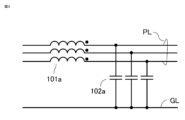
- FIG. 2 is a diagram showing the configuration of a passive filter.
- FIG. 7 is a diagram showing another configuration of a passive filter.
- 1 is a diagram showing the configuration of a noise filter according to Embodiment 1.
- FIG. 3 is a diagram showing another configuration of the noise filter according to the first embodiment.
- FIG. FIG. 3 is a diagram illustrating the principle of noise reduction of the noise filter according to the first embodiment.
- 3 is a diagram showing the configuration of a noise filter according to a second embodiment.
- FIG. 3 is a diagram showing another configuration of the noise filter according to Embodiment 2.
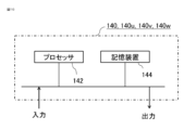
- FIG. 2 is a hardware configuration diagram that is an example of a compensation signal generation unit according to Embodiments 1 and 2.
- FIG. 1 is a diagram illustrating an example of a configuration of a power system to which a noise filter according to a first embodiment is applied.
- a noise filter 100 is attached to the power line PL along the route where power is supplied from the power supply 200 connected to the three-phase three-wire AC power line PL to the load 400 via the power converter 300. is connected.
- the noise filter 100 according to the present embodiment is not limited to the three-phase three-wire AC power line shown in FIG. , three-phase (three-wire or four-wire), between a power source and a power converter, between a power converter and a load, and between power converters if multiple power converters are provided. It may be a connection.
- the purpose of applying the noise filter 100 is, for example, to satisfy noise standards between the system power supply 200 and the power converter 300, and between the power converter 300 and the load 400.
- the ground leakage current of the motor which is a load, and the motor shaft voltage are suppressed.
- System power supply 200, noise filter 100, power converter 300, and load 400 are each connected to power line PL and to ground line GL.
- noise generation from the power converter 300 in the power system 1 will be described as a typical example of noise generation factors.
- a voltage-type three-phase full-bridge circuit will be described as an example of the power converter 300, but a current-type circuit, a circuit having a DC-DC conversion, a DC-AC conversion, an AC-DC conversion, or an AC-AC conversion function, or A circuit configuration such as a multilevel converter may also be used.
- FIG. 2 is a diagram showing the configuration of a voltage type three-phase full bridge circuit that is an example of the power converter 300.
- semiconductor switches SW11 to SW32 each include six semiconductor switching elements each having an anti-parallel diode.
- the semiconductor switches SW11, SW21, and SW31 on the positive side and the semiconductor switches SW12, SW22, and SW32 on the negative side are connected in series to form a leg, respectively, and three legs corresponding to the u-phase, v-phase, and w-phase are connected in parallel. are connected to form a three-phase full-bridge circuit.
- Each arm is connected to output terminals u, v, and w corresponding to the u-phase, v-phase, and w-phase, respectively, and is connected to the power line PL via the output terminals u, v, and w.
- a DC section is provided in parallel with the three-phase full bridge circuit, and in this DC section, a smoothing DC capacitor 310 and a DC voltage source (not shown) are connected in parallel with each other.
- the ground parasitic capacitance Zcm exists between each line and DC part of the three-phase full bridge circuit and the ground line GL.
- each of the semiconductor switching elements constituting the semiconductor switches SW11 to SW32 is, for example, a MOSFET (Metal Oxide Semiconductor Field Effect Transistor), an IGBT (Insulated Gate Bipo Self-extinguishing semiconductor elements such as LAR Transistor are used. .
- MOSFET Metal Oxide Semiconductor Field Effect Transistor
- IGBT Insulated Gate Bipo Self-extinguishing semiconductor elements such as LAR Transistor
- a preset voltage is output by the switching operation of semiconductor switches SW11 to SW32.
- a normal mode noise current flows between each output terminal due to the switching ripple voltage between the output terminals.
- a common mode voltage calculated by dividing the instantaneous sum of voltages at each output terminal by 3 is generated, and a common mode noise current flows through the ground parasitic capacitance Zcm and the ground line GL.
- Common mode noise differs from normal mode noise in that a noise current flows to the ground.
- FIG. 3 and 4 are diagrams showing examples of passive filters composed only of inductors and capacitors.
- the passive filter in FIG. 3 is composed of a common mode inductor 101a and a Y capacitor 102a, and is effective in attenuating the common mode component.
- the passive filter in FIG. 4 is composed of a normal mode inductor 101b and an be. Both figures show the case where a passive filter is applied in a three-phase three-wire system, and the black circles in the figures indicate the polarity of the common mode inductor.
- An inductor is a component whose impedance increases as the frequency increases, and by inserting it in series with a noise source, it suppresses noise propagation.
- a capacitor is a component whose impedance decreases as the frequency increases, and by inserting it in parallel with a noise source, it suppresses noise propagation.
- each phase winding is magnetically coupled using one magnetic component such as ferrite, and when a common mode noise current flows, the magnetic flux generated by each phase winding is generated within the magnetic component.
- They are inductors that strengthen each other.
- the magnetic fluxes weaken each other, so ideally the normal mode noise attenuation effect is not exhibited.
- the Y capacitor 102a is a capacitor connected between the power line PL of each phase and the ground line GL. Due to the existence of a path with low impedance at high frequency between the power line PL and the ground line GL on the common mode path, the noise current is returned to the ground line GL through the Y capacitor 102a, and the noise current is returned to the ground line GL to be protected or grounded. Noise flowing to the line GL can be suppressed.
- the normal mode inductor 101b is an inductor in which, when the windings of each phase are magnetically coupled with one magnetic component, the magnetic fluxes generated by the windings of each phase strengthen each other inside the magnetic component against the normal mode noise current. be. With respect to common mode current, the magnetic fluxes generated by the windings of each phase weaken each other within the magnetic component, so ideally the common mode noise attenuation effect is not exhibited. Furthermore, if the windings of each phase are not magnetically coupled by magnetic components, the magnetic fluxes generated by the windings of each phase do not interfere with each other, resulting in a normal mode inductor. Since an inductor is similarly connected to each phase, there is also an effect of attenuating common mode noise.
- the X capacitor 102b is a capacitor connected between each power line. Unlike the Y capacitor, it is not connected to the ground wire. Although the X capacitor 102b in FIG. 4 is illustrated as a Y connection with a neutral point in a three-phase three-wire AC power line, it may be connected in a ⁇ connection without a neutral point.
- the connection method for the X capacitor 102b can be selected depending on the required breakdown voltage and capacity. Inserting components that have low impedance at high frequencies has the effect of suppressing line voltage noise voltage against normal mode noise.
- the Y capacitor is a capacitor connected between each power line and the ground line, but the connection method is such that a capacitor is also inserted between the lines, and it also acts to attenuate normal mode components. However, since the capacitance of the Y capacitor is generally smaller than that of the X capacitor, the X capacitor is effective in attenuating the normal mode component.
- the zero-phase component or harmonic component of the grid power supply side transformer flows to the ground wire as a common mode noise current on the grid power supply side in the low frequency band.
- common mode noise currents caused by power grids are often dominated by commercial frequency components.
- the common mode noise current on the grid power supply side in the low frequency band is determined by the sum of that caused by the grid power supply and that caused by the power converter.
- the relationship between the Y capacitor capacity and the common mode noise current on the system power supply side in the low frequency band will be explained.
- the limit value is set by the standard for the purpose of preventing electric shock to the human body, so as mentioned above, there is a trade-off relationship between the common mode noise current caused by the grid power supply and the common mode noise current caused by the grid power supply.
- a normal mode or common mode current flowing on the grid power supply side in a high frequency band is measured using a LISN (Line Impedance Stabilization Network: pseudo power supply network) connected to the grid power supply side. Specifically, it is measured as a voltage (noise terminal voltage) generated when normal mode noise or common mode noise current flows through a terminal of LISN whose impedance is 50 ⁇ .
- the high frequency band is, for example, 150 kHz or higher, which corresponds to the conduction noise band, and the above measurement method is defined as a standard.
- the system power supply side of LISN has a low-pass filter configuration, and noise caused by the system power supply is not measured as a noise terminal voltage.
- the noise caused by the power converter connected to the load side of the LISN is measured as the noise terminal voltage.
- the noise caused by the power converter, measured as the noise terminal voltage is the sum of both normal mode or common mode.
- the larger the capacitance value of the Y capacitor the better.
- FIG. 5 is a diagram showing a configuration of the noise filter 100 according to the first embodiment
- FIG. 6 is a diagram showing another configuration of the noise filter 100 according to the first embodiment.
- a noise filter 100 that suppresses common mode noise on the grid power supply side includes a detection unit 120 that is connected to the power line PL and detects common mode noise, and a compensation signal generation unit 140 that generates a compensation signal that cancels out the common mode noise. , a compensation signal injection unit 130 that injects a compensation signal for canceling common mode noise into the power line PL.
- the detection unit 120 that detects common mode noise is composed of, for example, a Y-connected capacitor.
- the compensation signal generated by the compensation signal generation section 140 is, for example, a compensation voltage signal, and the output section of the compensation signal generation section 140 is connected to one terminal of the compensation signal injection section 130 and the input section of the compensation signal generation section 140. and output the generated compensation signals.
- the other terminal of the input section of the compensation signal generation section 140 is connected to the detection section 120.
- the compensation signal generation section 140 is connected to the ground line GL, and the output section of the compensation signal generation section 140 is connected in series between the compensation signal injection section 130 and the ground line GL.
- the compensation signal injection section 130 is composed of, for example, a Y-connected capacitor. Further, for example, an inductor 110 is connected to the power line PL for the purpose of increasing noise attenuation. For the purpose of increasing the amount of noise attenuation, a Y capacitor 150 may be further connected as shown in FIG. However, the inductor 110 and the Y capacitor 150 are not essential. In FIG. 6, the noise filter 100 is connected between the power line PL and the ground line GL, but the noise filter 100 may be connected only to the power line PL.
- a feature of the noise filter 100 according to the first embodiment is that the two input terminals of the input section of the compensation signal generation section 140 are differential inputs.
- the voltage of the common mode component of the capacitor forming the compensation signal injection section 130 is detected as a differential voltage.
- the compensation signal generation section 140 generates a voltage of, for example, the opposite polarity and one times or less as a compensation voltage, and outputs it in series between the compensation signal injection section 130 and the ground line GL. This cancels out the common mode voltage of the capacitor forming the compensation signal injection section 130 on the equivalent circuit of the common mode component. That is, in the configuration of noise filter 100 according to Embodiment 1, activating the capacitor forming compensation signal injection section 130 has the effect of making it function as a Y capacitor with increased apparent equivalent capacitance.
- FIG. 7 is an equivalent circuit diagram showing the operating principle of the noise filter 100 according to the first embodiment.
- connection points A and B are connection points A and B in FIG. 5, respectively. That is, the compensation signal injection section 130 and the compensation signal generation section 140 are connected in series between the power line PL and the ground line GL.
- a common mode noise current from a noise voltage source Vcm caused by a power converter flows to the power supply side and flows back to the load-to-ground parasitic capacitance Zm via the inductor 110, the power supply-to-ground impedance Zg, and the ground line GL.
- the role of the noise filter 100 is to reduce the amount of current flowing to the power supply side, that is, the power supply-to-ground impedance Zg.
- a common mode noise current Icm from a noise voltage source Vcm is a common mode noise current Ig flowing to the power supply side and a common mode noise current flowing to the compensation signal injection unit 130 side at a connection point A between the compensation signal injection unit 130 and the power line PL. It branches into Iy.
- the common mode voltage Vy is generated in the capacitor of the compensation signal injection section 130 by the common mode noise current Iy flowing to the compensation signal injection section 130 side.As described above, in the first embodiment, this common mode voltage Vy is detected. By doing so, the compensation signal generation unit 140 generates a voltage having the opposite polarity and one time or less of the common mode voltage Vy as the compensation voltage Vinj. That is, a compensation voltage Vinj satisfying equation (1) is generated as a compensation signal.
- equation (1) is a comparison of the absolute values of Vinj and Vy.
- the common mode voltage Vy is canceled out, and more of the common mode noise current Icm is distributed to the common mode noise current Iy.
- the common mode noise current Iy increases, the common mode noise current Ig flowing to the power supply side decreases.
- the common mode noise current Icm generated by the power converter is actively circulated to the capacitor side of the compensation signal injection unit 130, thereby reducing the common mode noise current Ig on the power supply side, which is the object of protection. It becomes possible to do so.
- the noise filter 100 according to the first embodiment forms a high-pass filter by the capacitor of the detection section 120 and the resistance component of the input section of the compensation signal generation section 140.
- the lower limit value of the compensation frequency can be set by designing the cutoff frequency of the high-pass filter, which is determined by the capacitance value of the capacitor of the detection section 120 and the resistance value of the input section of the compensation signal generation section 140.
- the common mode noise current of the dominant commercial frequency component caused by the grid power supply is, for example, 50 Hz or 60 Hz
- the frequency of the common mode noise current caused by the power converter is the dominant switching frequency component, It is approximately several kHz or more.
- the noise filter 100 according to the first embodiment has a function of substantially increasing the equivalent capacitance of the Y capacitor, and with respect to the common mode noise current of the commercial frequency component caused by the grid power supply, it is rather It has the effect of increasing
- the cutoff frequency of the high-pass filter formed by the capacitor of the detection unit 120 and the resistance component of the input part of the compensation signal generation unit 140 is set to be higher than the frequency of the common mode noise current caused by the grid power supply. Shifts the lower limit of the band to higher frequencies. Thereby, it is possible to suppress an increase in common mode noise current caused by the grid power supply.
- the equivalent capacitance of the Y capacitor is increased by setting the cutoff frequency of the high-pass filter to be lower than the switching frequency, which is the frequency of the common mode noise current caused by the power converter. This makes it possible to produce the effect of actively circulating the common mode current in the Y capacitor-power converter-load route via the grounding line GL. Therefore, the common mode noise current flowing through the power supply side can be reduced.
- the noise filter 100 has the effect of increasing the equivalent capacitance of the Y capacitor in a specific frequency range regardless of the cause of common mode current generation, so that the generation source is separated for each frequency band. Must have been. In other words, it is desirable that the frequency of the common mode noise current caused by the power system and the frequency of the common mode noise current caused by the power converter are divided. Therefore, if the frequency caused by the grid power source and the frequency caused by the power converter are close, the common mode noise current caused by the grid power source will increase, and the common mode noise current caused by the power converter will decrease. Become.
- the compensation signal generation section 140 included in the noise filter 100 according to the first embodiment in the low frequency range will be described.
- a general passive common mode filter configured only with a common mode inductor and a Y capacitor
- most of the common mode noise current source flows through the power supply side below the cutoff frequency.
- the capacitor of the compensation signal injection section 130 corresponds to the Y capacitor, and the compensation voltage increases the equivalent capacitance of the Y capacitor and lowers the impedance. .
- the switching frequency component of the common mode noise current which is a relatively low frequency caused by the power converter, is actively circulated to the capacitor of the compensation signal injection section 130.
- the capacitor of the compensation signal injection section 130 has a relatively low frequency, so it has a high impedance. Since the common mode noise current caused by the power converter is returned to the capacitor of the compensation signal injection section 130, it is determined by the product of the high impedance of the capacitor of the compensation signal injection section 130 and the common mode noise current. The maximum detected differential voltage and compensation voltage may become excessive.
- the maximum detected differential voltage corresponds to the maximum value of the common mode voltage Vy of the capacitor of the compensation signal injection section 130 shown in FIG. Therefore, if the maximum detected differential voltage becomes excessive, the compensation voltage for canceling it may also become excessive.
- the noise source impedance is, for example, approximately equal to the load-to-ground parasitic capacitance Zm, and the maximum compensation voltage is determined by the ratio of the load-to-ground parasitic capacitance Zm and the capacitance of the compensation signal injection section 130. Therefore, by making the capacitor capacity of the compensation signal injection section 130 sufficiently larger than the load-to-ground parasitic capacitance Zm, it is possible to suppress the maximum detected differential voltage and the compensation voltage.
- Compensation signal generation section 140 generally includes an operational amplifier, a transistor, and a control power supply. By suppressing the maximum differential detection voltage and the compensation voltage, the voltage of the control power supply necessary for the compensation signal generation section 140 and the slew rate and gain bandwidth of the compensation signal generation section 140 can be reduced. However, the upper limit value of the capacitance of the capacitor of the compensation signal injection section 130 is limited due to constraints on the low frequency common mode current flowing on the system power supply side caused by the system power supply.
- the high frequency range corresponds to the measurement range of conduction noise at the noise terminal voltage using LISN, and corresponds to the frequency range above the general cutoff frequency of a passive common mode filter.
- most of the common mode noise current flows back to the capacitor of the compensation signal injection section 130, which essentially functions as a Y capacitor.
- the common mode voltage component of the capacitor of the compensation signal injection section 130 functions as a small noise voltage source on the LISN side.
- the common mode voltage component can be canceled by generating and injecting a compensation voltage signal Vinj of polarity and magnitude less than or equal to one. This makes it possible to reduce the common mode component of the noise terminal voltage applied to the 50 ⁇ terminal of LISN. This shows that common mode noise can be suppressed in a high frequency range.
- the compensation voltage Vinj is generated so that a compensation voltage of 1 times the magnitude is output, that is, the magnitude of the gain is 1,
- Vy - Vinj 0, the connection point A and B are equivalent to a short circuit, and all the common mode noise current Icm from the noise voltage source Vcm is circulated to the capacitor of the compensation signal injection section 130. .
- the low frequency range refers to a frequency below the resonant frequency of the passive section composed of the capacitor of the compensation signal injection section 130 and the inductor on the power line PL.
- the common impedance on the system power supply side is approximately 0 ⁇
- the inductor 110 on the power line PL has a low impedance
- the capacitor of the compensation signal injection unit 130 has a high impedance.
- the compensation voltage Vinj is applied to almost all of the points.
- the detected differential voltage with respect to the generated compensation voltage has a phase of 0 degrees. Therefore, if the magnitude of the gain is 1, oscillation will occur.
- positive feedback control is performed in the low frequency range when the system power supply 200 is grounded.
- the magnitude of the gain of the compensation signal generation section 140 needs to be less than 1 in order to prevent oscillation caused by positive feedback. be.
- the impedance ZL of the inductor on the power line PL becomes high and the impedance of the capacitor of the compensation signal injection section 130 becomes low, so the detected differential voltage becomes smaller with respect to the output compensation voltage. . Therefore, the loop gain becomes small regardless of the power supply-to-ground impedance Zg on the power system side, so the gain of the compensation signal generation section 140 may be 1.
- the gain may be greater than 1 times as long as it is close to 1 times. If the gain exceeds 1, the noise attenuation effect will be reduced, but if the gain is close to 1 and is larger than 1, the effect will be equivalent to that of a gain that is close to 1 and less than 1.
- the noise filter 100 includes a detection section 120 that detects power line noise, a compensation signal generation section 140 that generates a compensation signal that attenuates the noise, and a compensation signal injection section 130 that injects the compensation signal. Since the compensation signal generation section 140 generates a compensation signal based on the difference signal between the input signal from the detection section 120 and the output signal of the compensation signal generation section 140, the compensation performance decreases in the low frequency range. is suppressed.
- the compensation signal injection section 130 is configured with a capacitor, a voltage due to a noise component is generated in the capacitor of the compensation signal injection section 130, and the compensation signal generation section 140 detects the voltage due to the noise component as a differential voltage. Since the compensation voltage is generated as a compensation signal so as to cancel the voltage due to the noise component, it is possible to efficiently compensate the generated noise in a wide frequency band.
- the compensation signal for canceling the noise component has the opposite polarity and the gain is set to around 1 times, but not more than 1 times. Further, in order to reduce noise in a low frequency range, if the gain of the compensation signal is 1, oscillation may occur in the circuit, which may affect noise reduction, so the gain is preferably less than 1. However, the gain may be 1 times outside the low frequency range.
- the compensation signal generation section 140 when the generated noise is in a low frequency range, the voltage of the capacitor of the compensation signal injection section 130 is detected, and the compensation signal generation section 140 generates a compensation voltage of the opposite polarity with a gain of less than 1 times that of the detected voltage. , are output in series between the compensation signal injector 130 and the ground line GL.
- feedforward control is used instead of feedback control that brings the detection noise closer to 0 using a compensation voltage. Therefore, in the configuration of the first embodiment, oscillation and a decrease in the detected amount due to resonance between the inductor on the power line PL and the capacitor of the compensation signal injection unit 130, which occur in conventional feedback control, do not occur. . Therefore, it is possible to perform compensation in a low frequency range below the resonant frequency of the inductor on the power line PL and the capacitor of the compensation signal injection section 130.
- the detection unit 120 and the compensation signal injection unit 130 by configuring the detection unit 120 and the compensation signal injection unit 130 with capacitors, it is possible to make the detection unit 120 and the compensation signal injection unit 130 smaller than the configuration in which the detection unit 120 and the compensation signal injection unit 130 are configured with inductors. be. This is because capacitors have higher energy density than inductors.
- Embodiment 1 when low frequency compensation is included as in Embodiment 1, a low frequency and large voltage is applied to the inductor, and in order to prevent magnetic saturation of the core, the core with a high saturation magnetic flux density needs to have a large cross-sectional area. There is. In other words, there is a concern that the inductor will become larger. Therefore, in this embodiment that performs low frequency compensation, by using a capacitor in the detection section 120 and the compensation signal injection section 130, the active noise filter can be more effectively miniaturized.
- FIG. 8 is a block diagram showing the configuration of a noise filter according to the second embodiment.
- the noise filter 100 according to the second embodiment includes detection units 120u, 120v, 120w, compensation signal injection units 130u, 130v, 130w, and compensation signal generation units 140u, 140v, 140w for each phase.
- the point is that it has a configuration in which The other configurations are the same as those in Embodiment 1, so the explanation will be omitted.
- the noise filter according to the first embodiment attenuates common mode noise on the power supply side, but the noise filter according to the second embodiment has the effect of attenuating normal mode noise and common mode noise on the power supply side.
- the detection units 120u, 120v, 120w and the compensation signal injection units 130u, 130v, 130w are connected between each power line PLu, PLv, PLw and the ground line GL, and are connected by the ground line GL. , it is possible to also detect the normal mode component between each phase line and inject a compensation signal.
- the sum of the common mode component between the power lines PLu, PLv, PLw of each phase and the ground line GL and the above-mentioned normal mode component is determined by the compensation signal injection unit 130u, 130v, 130w.
- the compensation signal generation units 140u, 140v, and 140w By detecting the differential voltage of the compensation signal injection sections 130u, 130v, and 130w, it is possible to detect the voltage that is the sum of the normal mode and common mode noises. Then, the compensation signal generation units 140u, 140v, and 140w generate compensation voltages of, for example, opposite polarity and one times the magnitude, and perform compensation in series between the compensation signal injection units 130u, 130v, and 130w and the ground line GL. By injecting voltage, it becomes possible to cancel the noise voltage of normal mode and common mode.
- a high-pass filter is formed by the capacitors of the detection sections 120u, 120v, and 120w and the resistances of the input sections of the compensation signal generation sections 140u, 140v, and 140w, and a high-pass filter is formed at an arbitrary compensation frequency. It is possible to set the lower limit of the band.
- a capacitor 150u, 150v and 150w may be provided in the noise filter 100 according to the second embodiment.
- FIG. 9 shows an example in which a capacitor is further provided in FIG. 8. Note that, as described in the first embodiment, the inductor 110 and the capacitors 150u, 150v, and 150w are not essential components. It may be provided as appropriate to enhance the noise attenuation effect.
- the noise filter 100 according to the second embodiment has a configuration in which detection units 120u, 120v, 120w, compensation signal injection units 130u, 130v, 130w, and compensation signal generation units 140u, 140v, 140w are arranged in each phase. , it is possible to detect the sum of the normal mode component and common mode component for the power line of each phase, and inject a corresponding compensation signal, making it possible to attenuate both normal mode noise and common mode noise. . Furthermore, since noise is actively suppressed, it is possible to downsize the X capacitor that constitutes the detection section and the compensation signal injection section.
- the compensation signal generation units 140, 140u, 140v, and 140w have a circuit configuration that generates a compensation voltage of opposite polarity to the voltage of the noise component detected from the differential voltage. , implementation can be simplified. Furthermore, the compensation signal is not limited to a voltage, but may be a compensation current.
- the circuit configuration of the compensation signal generation units 140, 140u, 140v, and 140w can be configured with an analog circuit using an operational amplifier, for example, as described above.
- the hardware configuration of the compensation signal generation units 140, 140u, 140v, and 140w includes a processor 142 (computer) and a storage device 144 as processing circuits, as shown in FIG. 10, for example.
- the processor 142 includes a CPU (Central Processing Unit), an ASIC (Application Specific Integrated Circuit), an IC (Integrated Circuit), and an FPGA (Fi eld Programmable Gate Array), various logic circuits, and various signal processing circuits, etc. good. Furthermore, a plurality of processors of the same type or different types may be provided as the processors 142, and each process may be shared and executed.
- the storage device 144 includes a RAM (Random Access Memory) that is configured to be able to read and write data from the processor 142, a ROM (Read Only Memory) that is configured to be able to read data from the processor 142, and the like. .
- the processor 142 executes a program input from a storage device 144 such as a ROM.
- a differential signal is calculated from the two input signals, and a gain corresponding to the noise frequency range is used to convert the differential signal to - A signal multiplied by 1 and a gain is calculated, and a corresponding signal is generated from a signal processing unit (not shown).
- the noise filter 100 is arranged between the power supply system 200 and the power converter 300, and the noise source caused by the power converter 300 has been explained. It may be placed between the load 400 and the load 400. It is possible to suppress the ground leakage current of the load 400 or the shaft voltage of the motor that is the load.
- the present invention also includes a configuration in which a plurality of noise filters according to Embodiment 1 that compensates for common mode noise are provided, and a configuration in which both noise filters in Embodiments 1 and 2 are provided.
Landscapes
- Filters And Equalizers (AREA)
- Stabilization Of Oscillater, Synchronisation, Frequency Synthesizers (AREA)
Priority Applications (2)
| Application Number | Priority Date | Filing Date | Title |
|---|---|---|---|
| PCT/JP2022/027055 WO2024009489A1 (ja) | 2022-07-08 | 2022-07-08 | ノイズフィルタ |
| JP2024531875A JP7693115B2 (ja) | 2022-07-08 | 2022-07-08 | ノイズフィルタ |
Applications Claiming Priority (1)
| Application Number | Priority Date | Filing Date | Title |
|---|---|---|---|
| PCT/JP2022/027055 WO2024009489A1 (ja) | 2022-07-08 | 2022-07-08 | ノイズフィルタ |
Publications (1)
| Publication Number | Publication Date |
|---|---|
| WO2024009489A1 true WO2024009489A1 (ja) | 2024-01-11 |
Family
ID=89453144
Family Applications (1)
| Application Number | Title | Priority Date | Filing Date |
|---|---|---|---|
| PCT/JP2022/027055 Ceased WO2024009489A1 (ja) | 2022-07-08 | 2022-07-08 | ノイズフィルタ |
Country Status (2)
| Country | Link |
|---|---|
| JP (1) | JP7693115B2 (https=) |
| WO (1) | WO2024009489A1 (https=) |
Citations (2)
| Publication number | Priority date | Publication date | Assignee | Title |
|---|---|---|---|---|
| JP2019080469A (ja) * | 2017-10-27 | 2019-05-23 | 三菱電機株式会社 | ノイズ低減装置 |
| JP6811904B1 (ja) * | 2020-03-24 | 2021-01-13 | 三菱電機株式会社 | ノイズ低減装置 |
-
2022
- 2022-07-08 WO PCT/JP2022/027055 patent/WO2024009489A1/ja not_active Ceased
- 2022-07-08 JP JP2024531875A patent/JP7693115B2/ja active Active
Patent Citations (2)
| Publication number | Priority date | Publication date | Assignee | Title |
|---|---|---|---|---|
| JP2019080469A (ja) * | 2017-10-27 | 2019-05-23 | 三菱電機株式会社 | ノイズ低減装置 |
| JP6811904B1 (ja) * | 2020-03-24 | 2021-01-13 | 三菱電機株式会社 | ノイズ低減装置 |
Also Published As
| Publication number | Publication date |
|---|---|
| JPWO2024009489A1 (https=) | 2024-01-11 |
| JP7693115B2 (ja) | 2025-06-16 |
Similar Documents
| Publication | Publication Date | Title |
|---|---|---|
| Xing et al. | Conducted common-mode EMI reduction by impedance balancing | |
| EP2787618B1 (en) | Voltage fed feed forward active EMI filter | |
| Chen et al. | A novel inverter-output passive filter for reducing both differential-and common-mode $ dv/dt $ at the motor terminals in PWM drive systems | |
| JP4260110B2 (ja) | フィルタ装置 | |
| JP3393374B2 (ja) | 電力変換システム | |
| US20140268933A1 (en) | Filter device, power converter and common mode noise suppression method | |
| JP2863833B2 (ja) | アクティブコモンモードキャンセラ | |
| KR102315575B1 (ko) | 공통 모드 전류를 감소시키는 방법 | |
| Kume et al. | Integrated filters and their combined effects in matrix converter | |
| US20170288575A1 (en) | Power converter | |
| Amin et al. | A review on recent characterization effort of CM EMI in power electronics system with emerging wide band gap switch | |
| JP6771693B1 (ja) | 電力変換装置 | |
| JP2001268890A (ja) | 電力変換システム | |
| Liu et al. | Insertion loss analysis and optimization of a current based common-mode active EMI filter | |
| JP6207751B2 (ja) | 電力変換装置 | |
| JP7374332B2 (ja) | 電力変換装置 | |
| JP2001231268A (ja) | 電力変換装置 | |
| Chen et al. | Common-mode noise reduction with impedance balancing in DC-fed motor drives | |
| CN102282748B (zh) | 输出滤波器以及具备输出滤波器的电力变换装置 | |
| JP7693115B2 (ja) | ノイズフィルタ | |
| JP6251221B2 (ja) | ノイズフィルタ装置 | |
| JP6178178B2 (ja) | ノイズフィルタ | |
| Han et al. | Suppressing methods of common-mode noise in LLC resonant DC-DC converters | |
| KR20210041362A (ko) | 태양광 발전기용 전류 보상 시스템 | |
| Sun et al. | Investigation and suppression of conducted EMI and shaft voltage in induction motor drive system |
Legal Events
| Date | Code | Title | Description |
|---|---|---|---|
| 121 | Ep: the epo has been informed by wipo that ep was designated in this application |
Ref document number: 22950283 Country of ref document: EP Kind code of ref document: A1 |
|
| ENP | Entry into the national phase |
Ref document number: 2024531875 Country of ref document: JP Kind code of ref document: A |
|
| NENP | Non-entry into the national phase |
Ref country code: DE |
|
| 122 | Ep: pct application non-entry in european phase |
Ref document number: 22950283 Country of ref document: EP Kind code of ref document: A1 |