WO2024004147A1 - 半導体製造装置用部材 - Google Patents
半導体製造装置用部材 Download PDFInfo
- Publication number
- WO2024004147A1 WO2024004147A1 PCT/JP2022/026285 JP2022026285W WO2024004147A1 WO 2024004147 A1 WO2024004147 A1 WO 2024004147A1 JP 2022026285 W JP2022026285 W JP 2022026285W WO 2024004147 A1 WO2024004147 A1 WO 2024004147A1
- Authority
- WO
- WIPO (PCT)
- Prior art keywords
- gas
- passage
- insulating sleeve
- base plate
- semiconductor manufacturing
- Prior art date
- Legal status (The legal status is an assumption and is not a legal conclusion. Google has not performed a legal analysis and makes no representation as to the accuracy of the status listed.)
- Ceased
Links
Images


Classifications
-
- H—ELECTRICITY
- H10—SEMICONDUCTOR DEVICES; ELECTRIC SOLID-STATE DEVICES NOT OTHERWISE PROVIDED FOR
- H10P—GENERIC PROCESSES OR APPARATUS FOR THE MANUFACTURE OR TREATMENT OF DEVICES COVERED BY CLASS H10
- H10P72/00—Handling or holding of wafers, substrates or devices during manufacture or treatment thereof
- H10P72/70—Handling or holding of wafers, substrates or devices during manufacture or treatment thereof for supporting or gripping
- H10P72/72—Handling or holding of wafers, substrates or devices during manufacture or treatment thereof for supporting or gripping using electrostatic chucks
- H10P72/722—Details of electrostatic chucks
-
- H—ELECTRICITY
- H10—SEMICONDUCTOR DEVICES; ELECTRIC SOLID-STATE DEVICES NOT OTHERWISE PROVIDED FOR
- H10P—GENERIC PROCESSES OR APPARATUS FOR THE MANUFACTURE OR TREATMENT OF DEVICES COVERED BY CLASS H10
- H10P72/00—Handling or holding of wafers, substrates or devices during manufacture or treatment thereof
- H10P72/70—Handling or holding of wafers, substrates or devices during manufacture or treatment thereof for supporting or gripping
- H10P72/76—Handling or holding of wafers, substrates or devices during manufacture or treatment thereof for supporting or gripping using mechanical means, e.g. clamps or pinches
- H10P72/7604—Handling or holding of wafers, substrates or devices during manufacture or treatment thereof for supporting or gripping using mechanical means, e.g. clamps or pinches the wafers being placed on a susceptor, stage or support
- H10P72/7624—Handling or holding of wafers, substrates or devices during manufacture or treatment thereof for supporting or gripping using mechanical means, e.g. clamps or pinches the wafers being placed on a susceptor, stage or support characterised by the mechanical construction of the susceptor, stage or support
-
- H—ELECTRICITY
- H10—SEMICONDUCTOR DEVICES; ELECTRIC SOLID-STATE DEVICES NOT OTHERWISE PROVIDED FOR
- H10P—GENERIC PROCESSES OR APPARATUS FOR THE MANUFACTURE OR TREATMENT OF DEVICES COVERED BY CLASS H10
- H10P72/00—Handling or holding of wafers, substrates or devices during manufacture or treatment thereof
- H10P72/04—Apparatus for manufacture or treatment
- H10P72/0431—Apparatus for thermal treatment
- H10P72/0432—Apparatus for thermal treatment mainly by conduction
-
- H—ELECTRICITY
- H10—SEMICONDUCTOR DEVICES; ELECTRIC SOLID-STATE DEVICES NOT OTHERWISE PROVIDED FOR
- H10P—GENERIC PROCESSES OR APPARATUS FOR THE MANUFACTURE OR TREATMENT OF DEVICES COVERED BY CLASS H10
- H10P72/00—Handling or holding of wafers, substrates or devices during manufacture or treatment thereof
- H10P72/04—Apparatus for manufacture or treatment
- H10P72/0431—Apparatus for thermal treatment
- H10P72/0434—Apparatus for thermal treatment mainly by convection
-
- H—ELECTRICITY
- H10—SEMICONDUCTOR DEVICES; ELECTRIC SOLID-STATE DEVICES NOT OTHERWISE PROVIDED FOR
- H10P—GENERIC PROCESSES OR APPARATUS FOR THE MANUFACTURE OR TREATMENT OF DEVICES COVERED BY CLASS H10
- H10P72/00—Handling or holding of wafers, substrates or devices during manufacture or treatment thereof
- H10P72/04—Apparatus for manufacture or treatment
- H10P72/0448—Apparatus for applying a liquid, a resin, an ink or the like
-
- H—ELECTRICITY
- H10—SEMICONDUCTOR DEVICES; ELECTRIC SOLID-STATE DEVICES NOT OTHERWISE PROVIDED FOR
- H10P—GENERIC PROCESSES OR APPARATUS FOR THE MANUFACTURE OR TREATMENT OF DEVICES COVERED BY CLASS H10
- H10P72/00—Handling or holding of wafers, substrates or devices during manufacture or treatment thereof
- H10P72/70—Handling or holding of wafers, substrates or devices during manufacture or treatment thereof for supporting or gripping
- H10P72/72—Handling or holding of wafers, substrates or devices during manufacture or treatment thereof for supporting or gripping using electrostatic chucks
Definitions
- the present invention relates to a member for semiconductor manufacturing equipment.
- an electrostatic chuck that includes a ceramic plate with built-in electrodes and a wafer mounting surface on its upper surface, and a metal base plate bonded to the lower surface of the ceramic plate.
- Patent Document 1 discloses that such an electrostatic chuck includes a gas common passage provided inside the ceramic plate in parallel with the wafer placement surface, a plurality of gas outflow passages from the gas common passage to the wafer placement surface, and a base plate. A gas inflow passage that penetrates in the vertical direction and communicates with a common gas passage is disclosed.
- the present invention has been made to solve such problems, and its main purpose is to prevent differences in the flow rates of gas flowing out from a plurality of gas outflow passages communicating with a common gas passage.
- the member for semiconductor manufacturing equipment of the present invention includes: A member for semiconductor manufacturing equipment comprising a wafer mounting surface, a plurality of gas outflow passages opening to the wafer mounting surface; a gas common passage provided inside the semiconductor manufacturing equipment member and communicating with the plurality of gas outflow passages; A number of gas inflow passages that communicate with the gas common passage from a surface of the member for semiconductor manufacturing equipment opposite to the wafer mounting surface and that are smaller in number than the number of gas outflow passages that communicate with the gas common passage; , Equipped with Among the plurality of gas outflow passages, those closer to the gas inflow passage have a higher gas passage resistance than those farther from the gas inflow passage. It is something.
- the gas introduced into the gas inflow passage passes through the gas common passage, is distributed to a plurality of gas outflow passages provided in the gas common passage, and passes through the gas outflow passage to the wafer mounting surface. leaks to. Since the number of gas inflow passages is smaller than the number of gas outflow passages, the number of gas introduction pipes externally connected to the gas inflow passages can be reduced. Further, among the plurality of gas outflow passages, those closer to the gas inflow passage have a higher gas passage resistance than those farther from the gas inflow passage. Therefore, there is no large difference in the flow rate of gas flowing out from the plurality of gas outflow passages communicating with the gas common passage. Therefore, it is possible to suppress the occurrence of defects due to temperature unevenness in the wafer.
- the gas passage resistance is determined by the length or cross-sectional area of the spiral portion provided in the gas outflow passage. Alternatively, the length or density of the porous portion provided in the gas outflow passage may be adjusted. In this way, the gas passage resistance can be adjusted with a relatively simple configuration.
- the member for semiconductor manufacturing equipment of the present invention includes a ceramic plate having the wafer mounting surface on the upper surface and incorporating an electrode; a conductive base plate provided on the lower surface of the ceramic plate; the gas common passage and the gas inflow passage may be provided in the base plate; and the gas outflow passage may be provided in the base plate; It may be provided on the base plate and the ceramic plate so as to reach the wafer mounting surface from the common gas passage.
- the base plate may have a refrigerant flow path, and the common gas passage is connected to the base plate.
- the gas passage resistance may be provided below the refrigerant flow path, and the gas passage resistance may be adjusted in a portion of the gas outflow path from the gas common path to the upper surface of the base plate. In this way, since the portion from the gas common passage to the upper surface of the base plate is relatively long, the gas passage resistance can be adjusted relatively easily by utilizing that long portion.
- the base plate includes an insulating sleeve in a base plate through hole that vertically passes through the base plate.
- the insulating sleeve may include a first communication hole forming a part of the gas common passage, and a first communication hole extending from the first communication hole to an upper surface of the insulating sleeve, and the insulating sleeve forming a part of the gas outflow passage. and a second communication hole forming a part of the insulating sleeve, and the gas passage resistance may be adjusted by the second communication hole of the insulating sleeve.
- the gas passage resistance can be adjusted using the insulating sleeve that is separate from the ceramic plate and the base plate. Additionally, if the second communication hole of the insulating sleeve, which is part of the gas outflow passage, deteriorates due to the use of components for semiconductor manufacturing equipment, it is possible to remove the insulating sleeve from the bottom side of the base plate and attach a new insulating sleeve. can. Therefore, discharge prevention maintenance can be easily carried out.
- the insulating sleeve may be a single member that cannot be separated. This makes the replacement work easier than when the insulating sleeve is made up of multiple members.
- the first communication hole of the insulating sleeve is connected to the second communication hole in a plan view. They may be provided radially in at least three directions with the center at the center. In this way, when the insulating sleeve is inserted into the base plate through hole, the gas flowing through the common gas passage can be sent to the gas outflow passage regardless of the rotational position of the insulating sleeve.
- the outer diameter of the insulating sleeve is larger than the width of the common gas passage. It can be small. In this way, a portion of the gas flowing from the upstream side of the common gas passage can pass through the outside of the insulating sleeve and proceed to the downstream side of the common gas passage.
- the ceramic plate and the base plate are bonded by a conductive bonding layer.
- the insulating sleeve may be inserted into the conductive bonding layer. In this way, the portion of the gas outflow passage that passes through the conductive bonding layer is also covered by the insulating sleeve, so that it is possible to prevent discharge from occurring in that portion.
- the upper surface of the insulating sleeve is connected to the ceramic via an upper resin adhesive layer.
- the lower surface of the insulating sleeve may be attached to the base plate via a lower resin adhesive layer or a sealant.
- FIG. 3 is a plan view of the wafer mounting table 10.
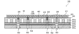
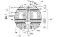
- FIG. AA sectional view of FIG. 1. A partially enlarged view of FIG. 2.
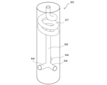
- FIG. 6 is a perspective view of an insulating sleeve 60.
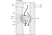
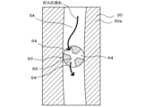
- FIG. 3 is a cross-sectional view of a cut surface of the wafer mounting table 10 taken along a horizontal plane passing through a common gas passage 54 when viewed from above.
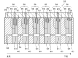
- FIG. 5 is a schematic explanatory diagram of a gas inflow passage 52, a gas common passage 54, and a gas outflow passage 56.
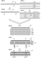
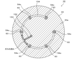
- FIG. 4 is a manufacturing process diagram of the wafer mounting table 10. An explanatory diagram of a gas common passage 154.
- FIG. AA sectional view of FIG. 1.
- FIG. 2 is a perspective view of an insulating sleeve 60.
- FIG. 3 is a cross-sectional view of a cut surface of the wafer mounting table 10 taken along a horizontal plane passing through a
- FIG. 3 is a perspective view of an insulating sleeve 160.
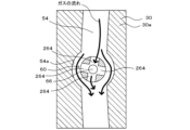
- FIG. 6 is an explanatory diagram of an insulating sleeve 60 including a first communication hole 264.
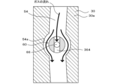
- FIG. 6 is an explanatory diagram of an insulating sleeve 60 including a first communication hole 364.
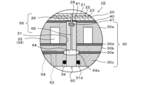
- FIG. 7 is an explanatory diagram of an example in which a seal ring 39 is arranged at the lower part of an insulating sleeve 60.
- FIG. 6 is an explanatory diagram of an example in which the outer diameter of the insulating sleeve 60 and the width of the gas common passage 54 are substantially the same.
- FIG. 1 is a plan view of the wafer mounting table 10
- FIG. 2 is a sectional view taken along line AA in FIG. 1
- FIG. 3 is a partially enlarged view of FIG. 5 is a cross-sectional view of the wafer mounting table 10 cut along a horizontal plane passing through the gas common passage 54, viewed from above.
- FIG. 6 is a partially enlarged view of FIG. )
- FIG. 7 are schematic explanatory views of the gas inflow passage 52, the gas common passage 54, and the gas outflow passage 56.
- “upper” and “lower” do not represent an absolute positional relationship, but represent a relative positional relationship. Therefore, depending on the orientation of the wafer mounting table 10, "top” and “bottom” can become “bottom”, “top”, “left”, “right”, “front”, and “rear”.
- the wafer mounting table 10 is an example of a member for semiconductor manufacturing equipment of the present invention, and as shown in FIG. It includes a passage 52, a gas outflow passage 56, and an insulating sleeve 60.
- the ceramic plate 20 is a circular plate (for example, 300 mm in diameter and 5 mm in thickness) made of ceramic such as an alumina sintered body or an aluminum nitride sintered body.
- the upper surface of the ceramic plate 20 serves as a wafer placement surface 21 on which a wafer W is placed.
- the ceramic plate 20 incorporates an electrostatic electrode 22 and a heater electrode 23 in order from the wafer placement surface 21 .
- an annular seal band 21a is formed along the outer edge, and a plurality of small circular protrusions 21b are formed on the entire inner surface of the seal band 21a. There is.
- the seal band 21a and the small circular protrusion 21b have the same height, and the height is, for example, several ⁇ m to several tens of ⁇ m.
- a portion of the wafer mounting surface 21 where the seal band 21a and small circular projections 21b are not provided is referred to as a reference surface 21c.
- the ceramic plate 20 has a gas ejection hole 26 that constitutes a part of the gas outflow passage 56 .
- a plurality of gas ejection holes 26 (six in this case) are provided concentrically with the ceramic plate 20. The gas ejection holes 26 are open to the reference surface 21c of the wafer mounting surface 21.
- the electrostatic electrode 22 is a planar mesh electrode, and is connected to an external DC power source via a power supply member (not shown).
- the power supply member is electrically insulated from the conductive bonding layer 40 and the base plate 30.
- the heater electrode 23 is a resistance heating element that is wired in a single stroke across the entire ceramic plate 20 from one end to the other end in a plan view.
- a heater power source is connected to one end and the other end of the heater electrode 23 via a power supply member (not shown).
- the power supply member is electrically insulated from the conductive bonding layer 40 and the base plate 30. When the heater electrode 23 is energized, it generates heat and heats the wafer mounting surface 21 and, in turn, the wafer W.
- the base plate 30 is a disk with good electrical conductivity and thermal conductivity (a disk with the same diameter as the ceramic plate 20 or a larger diameter).
- the base plate 30 is made by joining a first layer 30a, a second layer 30b, and a third layer 30c with conductive bonding layers 30d and 30e.
- a refrigerant flow path 32 through which refrigerant circulates is formed inside the base plate 30.
- the coolant flow path 32 includes a coolant flow groove 34, which is a concave groove provided on the lower surface of the first layer 30a, and a conductive bonding layer 30d that closes the lower opening of the coolant flow groove 34.
- the refrigerant flowing through the refrigerant channel 32 is preferably liquid and preferably electrically insulating. Examples of the electrically insulating liquid include fluorine-based inert liquids.
- the coolant flow path 32 is formed in a single stroke across the entire base plate 30 from one end (inlet) to the other end (exit) in plan view.
- a supply port and a recovery port of an external refrigerant device are connected to one end and the other end of the refrigerant flow path 32, respectively.
- the refrigerant supplied from the supply port of the external refrigerant device to one end of the refrigerant flow path 32 passes through the refrigerant flow path 32, returns to the recovery port of the external refrigerant device from the other end of the refrigerant flow path 32, and is then temperature-adjusted.
- the refrigerant is again supplied to one end of the refrigerant flow path 32 from the supply port.
- the base plate 30 is connected to a radio frequency (RF) power source and is also used as an RF electrode.
- RF radio frequency
- Examples of the material of the base plate 30 include a metal material and a composite material of metal and ceramic.
- Examples of the metal material include Al, Ti, Mo, and alloys thereof.
- Examples of composite materials of metal and ceramic include metal matrix composites (MMC) and ceramic matrix composites (CMC). Specific examples of such composite materials include materials containing Si, SiC and Ti (also referred to as SiSiCTi), materials in which porous SiC is impregnated with Al and/or Si, composite materials of Al 2 O 3 and TiC, etc. can be mentioned. It is preferable to select a material for the base plate 30 that has a coefficient of thermal expansion close to that of the material for the ceramic plate 20.
- the first layer 30a, the second layer 30b, and the third layer 30c are made of the above-mentioned metal material or a composite material of metal and ceramic, and the conductive bonding layers 30d and 30e are the conductive bonding layers described below. It may be made of the same material as 40.
- the conductive bonding layer 40 is, for example, a metal bonding layer, and bonds the lower surface of the ceramic plate 20 and the upper surface of the base plate 30.
- the conductive bonding layer 40 is formed by, for example, TCB (thermal compression bonding).
- TCB is a known method in which a metal bonding material is sandwiched between two members to be joined, and the two members are pressure bonded while being heated to a temperature below the solidus temperature of the metal bonding material.
- the gas common passage 54 is provided inside the base plate 30 in parallel to the wafer mounting surface 21 (that is, in the horizontal direction). Note that “parallel” means not only completely parallel, but even if not completely parallel, it is considered parallel as long as it is within an allowable error (for example, tolerance). As shown in FIG. 2, the gas common passage 54 is a passage provided between the second layer 30b and the third layer 30c of the base plate 30, and is provided below the refrigerant flow path 32. The vertical height of the gas common passage 54 includes the vertical height (thickness) of the conductive bonding layer 30e. As shown in FIG.
- the gas common passage 54 is formed in a C-shape (arc shape) in a plan view, and has a plurality of (six in this case) sleeve insertion portions 54a from one end to the other end.
- the sleeve insertion portion 54 a is a portion where the gas common passage 54 bulges in an arc shape when viewed from above, and its inner diameter is larger than the outer diameter of the insulating sleeve 60 . Therefore, a space through which gas can pass is formed between the arc-shaped wall of the sleeve insertion portion 54a and the insulating sleeve 60.
- the plurality of sleeve insertion portions 54a are provided at approximately equal intervals along the gas common passage 54.
- the plurality of insulating sleeves 60 are provided at approximately equal intervals on a concentric circle that forms the outer shape of the wafer mounting table 10 .
- a plurality of gas outflow passages 56 are provided for one gas common passage 54 so as to extend from the gas common passage 54 to the reference surface 21c of the wafer mounting surface 21.
- the gas inflow passage 52 is provided so as to extend from the lower surface of the base plate 30 (the surface of the wafer mounting table 10 opposite to the wafer mounting surface 21) to one end of the gas common passage 54.
- the number of gas inflow passages 52 is smaller than the number of gas outflow passages 56 communicating with the gas common passage 54, in this case one gas inflow passage 52 is provided.
- the insulating sleeve 60 is arranged in a base plate through hole 31 that vertically passes through the base plate 30.
- Insulating sleeve 60 is made of an electrically insulating material (eg, the same material as ceramic plate 20).
- the base plate through hole 31 is provided so as not to penetrate the coolant flow path 32.
- the insulating sleeve 60 is a single cylindrical body that cannot be separated, and has a first communication hole 64 forming a part of the gas common passage 54 and a first communication hole 64 forming a part of the gas outflow passage 56. It has two communicating holes 66.
- the first communication hole 64 is provided along the horizontal direction. In this embodiment, as shown in FIG.
- the first communication holes 64 are formed radially in three directions at equal angles (or approximately equal angles) around the second communication hole 66 when viewed from above. ing. It is preferable that the first communication hole 64 expands in diameter from the center of the insulating sleeve 60 in a radially outward direction.
- the second communicating hole 66 is provided along the central axis of the insulating sleeve 60 from the intersection of the plurality of first communicating holes 64 to the upper surface of the insulating sleeve 60.
- the second communication hole 66 constitutes a gas outflow passage 56 together with the gas ejection hole 26 of the ceramic plate 20 .
- the second communication hole 66 has a spiral portion 67 . As shown in FIG.
- the upper part of the insulating sleeve 60 is inserted into a bonding layer through hole 41 that vertically penetrates the conductive bonding layer 40, and is bonded to the ceramic plate 20 via an insulating resin bonding layer 28. ing.
- the lower portion of the base plate through hole 31 is a large diameter portion 31d having a larger diameter than other portions.
- the lower part of the insulating sleeve 60 is adhesively fixed by a resin adhesive layer 38 filled between the insulating sleeve 60 and the large diameter portion 31d of the base plate through hole 31.
- FIG. 7 shows a cross-sectional view of the wafer mounting table 10 taken in the vertical direction along the center line of the C-shaped common gas passage 54 and expanded into a plane. Since FIG. 7 is an explanatory diagram showing the connection relationship between the gas inflow passage 52, the gas common passage 54, and the gas outflow passage 56, components unrelated to these are omitted.
- the length of the spiral portion 67 of the plurality of insulating sleeves 60 is longer as it is closer to the gas inflow passage 52 (ie, upstream), and shorter as it is farther from the gas inflow passage 52 (ie, downstream).
- the gas passage resistance of the plurality of insulating sleeves 60 increases as the insulating sleeves 60 are closer to the gas inflow passage 52, and decreases as they are farther from the gas inflow passage 52.
- the length of the spiral portion 67 may be determined by the number of turns of the spiral portion 67. In this way, the gas passage resistance is adjusted in the portion of the gas outflow passage 56 from the gas common passage 54 to the upper surface of the base plate 30, that is, the second communication hole 66.
- the length of the spiral portion 67 of each insulating sleeve 60 is set so that the flow rate of gas ejected from each gas ejection hole 26 is the same (or almost the same) when gas is introduced into the gas inflow passage 52. .
- FIG. 8 is a manufacturing process diagram of the wafer mounting table 10.
- a ceramic plate 20 containing an electrostatic electrode 22 and a heater electrode 23 is prepared (FIG. 8A).
- the ceramic plate 20 is obtained by producing a molded body of ceramic powder containing the electrostatic electrode 22 and the heater electrode 23, and hot press firing the molded body.
- gas ejection holes 26 are formed in the ceramic plate 20 (FIG. 8B).
- first to third layers 30a to 30c made of MMC are prepared (FIG. 8C). Then, appropriate grooves and holes are formed in the first to third layers 30a to 30c by machining (FIG. 8D). Specifically, coolant channel grooves 34 are formed on the lower surface of the first layer 30a. At the same time, a first layer through hole 31a is formed in the first layer 30a to vertically penetrate the first layer 30a. Further, a second layer through hole 31b is formed in the second layer 30b to vertically penetrate the second layer 30b, and a third layer with a step is formed in the third layer 30c to vertically penetrate the third layer 30c. A through hole 31c is formed.
- the first layer through hole 31a to the third layer through hole 31c constitute the base plate through hole 31. Furthermore, grooves (not shown) that will eventually become the gas common passage 54 are formed on the lower surface of the second layer 30b and the upper surface of the third layer 30c.
- the first to third layers 30a to 30c are preferably made of SiSiCTi or AlSiC. This is because the coefficient of thermal expansion of alumina and the coefficient of thermal expansion of SiSiCTi or AlSiC can be made approximately the same.
- a layer (disk member) made of SiSiCTi can be produced, for example, as follows. First, a powder mixture is prepared by mixing silicon carbide, metal Si, and metal Ti. Next, the obtained powder mixture is uniaxially pressed to produce a disk-shaped compact, and the compact is hot-press sintered in an inert atmosphere to obtain a disk member made of SiSiCTi. .
- a metal bonding material 82 is placed between the third layer 30c and the second layer 30b, a metal bonding material 81 is placed between the second layer 30b and the first layer 30a, and the first layer 30a and the metal bonding material 81 are placed between the second layer 30b and the first layer 30a.
- a metal bonding material 80 is placed between the ceramic plate 20 (FIG. 8E). Through holes are previously provided in the metal bonding materials 80, 81, and 82 at positions facing the first layer through holes 31a to the third layer through holes 31c. Furthermore, a through hole (long hole) is previously provided in the metal bonding material 81 at a position where the gas common passage 54 is to be formed.
- the bodies are joined together under pressure and then returned to room temperature.
- the first layer 30a to the third layer 30c are joined by the conductive joining layers 30d and 30e in which the metal joining materials 81 and 82 have been changed to form the base plate 30, and the ceramic plate 20 and the base plate 30 are are bonded by a modified conductive bonding layer 40 (FIG. 8F).
- the first layer through hole 31a to the third layer through hole 31c are connected to form the base plate through hole 31.
- an Al--Mg-based bonding material or an Al--Si--Mg-based bonding material can be used.
- the laminate is pressurized while being heated in a vacuum atmosphere.
- Such an insulating sleeve 60 can be manufactured according to the "manufacturing method of three-dimensional fired body" of WO2020/217406.
- an insulating sleeve molded body is produced.
- the insulating sleeve molded body becomes the insulating sleeve 60 after firing.
- the dimensions of the insulating sleeve molded body are determined based on the dimensions of the insulating sleeve 60, taking into account that it will be baked during firing.
- the insulating sleeve molded body is produced using a mold.
- the mold has a core inside a cup-shaped (bottomed cylindrical) main body.
- the internal space (molding space) of the mold excluding the core has the same shape as the insulating sleeve molded product.
- the mold is manufactured using a well-known 3D printer.
- a 3D printer repeats a series of operations in which a precured material is discharged from a head portion toward a stage to form a precured layered material, and the precured layered material is cured.
- model material which is the material that makes up the final necessary parts of the mold
- part of the mold that is the base part that supports the model material and is ultimately removed. and support materials constituting the structure.
- model material we use a material (e.g., wax such as paraffin wax) that is insoluble in the specified cleaning liquid (water, organic solvent, acid, alkaline solution, etc.), and as the support material, we use a material that is soluble in the specified cleaning liquid (for example, hydroxylated waxes) are used.
- a 3D printer models a structure using slice data that is sliced horizontally into layers from the bottom to the top of a mold at predetermined intervals. Slice data is created by processing CAD data. Among the slice data, there is slice data that includes a mixture of model material and support material, and there is slice data that includes only model material.
- a structure formed by a 3D printer is immersed in a cleaning liquid to dissolve and remove the hardened support material, thereby obtaining an object, ie, a mold, made only of the hardened model material.
- the insulating sleeve molded body is produced by mold casting using this mold. Specifically, a ceramic slurry containing ceramic powder, a solvent, a dispersant, and a gelling agent is injected into the molding space of the mold, and the gelling agent is caused to undergo a chemical reaction to gel the ceramic slurry. An insulating sleeve molded body is produced inside the mold. Thereafter, the insulating sleeve molded body is obtained by melting or burning away only the molding die in which the insulating sleeve molded body has been produced. Finally, the insulating sleeve molded body is fired and the external dimensions of the fired body are adjusted to obtain the insulating sleeve 60.
- the wafer W is placed on the wafer placement surface 21 with the wafer placement table 10 installed in a chamber (not shown). Then, the inside of the chamber is depressurized by a vacuum pump and adjusted to a predetermined degree of vacuum, and a DC voltage is applied to the electrostatic electrode 22 of the ceramic plate 20 to generate electrostatic adsorption force, and the wafer W is placed on the wafer. It is suctioned and fixed to the surface 21 (specifically, the upper surface of the seal band 21a or the upper surface of the small circular protrusion 21b).
- the heater electrode 23 is energized to cause the ceramic plate 20 to generate heat, thereby heating the wafer W to a predetermined temperature.
- backside gas is introduced into the gas inlet passage 52 from a gas cylinder (not shown).
- a thermally conductive gas for example, He gas
- the backside gas introduced into the gas inflow passage 52 passes through the gas common passage 54 and is distributed to a plurality of gas outflow passages 56 to fill the space ( A space surrounded by the back surface of the wafer W, the seal band 21a of the wafer mounting surface 21, the circular small protrusion 21b, and the reference surface 21c is filled and sealed.
- This backside gas allows efficient heat conduction between the wafer W and the ceramic plate 20.
- the inside of the chamber is made into a reaction gas atmosphere at a predetermined pressure (for example, several tens to several hundreds of Pa), and in this state, there is a gap between an upper electrode (not shown) provided on the ceiling of the chamber and the base plate 30 of the wafer mounting table 10.
- Plasma is generated by applying an RF voltage.
- the surface of the wafer W is processed by the generated plasma.
- a refrigerant is circulated through the refrigerant flow path 32 of the base plate 30 at appropriate times.
- the thermally conductive gas that has flowed into the gas inflow passage 52 reaches the insulating sleeve 60 from the upstream side of the sleeve insertion portion 54a of the gas common passage 54, and a part of it reaches the first insulating sleeve 60. It flows into the communication hole 64. A part of the gas that has flowed into the first communication hole 64 is supplied to the space on the back surface of the wafer W via the second communication hole 66 and the gas ejection hole 26 (that is, the gas outflow passage 56), and the rest is supplied to the space on the back surface of the wafer W.
- the gas passes through the communication hole 64 and flows to the downstream side of the insulating sleeve 60 in the gas common passage 54 . Further, the gas that has not flowed into the first communication hole 64 of the insulating sleeve 60 flows to the downstream side of the insulating sleeve 60 through the gap between the insulating sleeve 60 and the sleeve insertion portion 54a of the gas common passage 54.
- the backside gas Before the backside gas fills the space between the back surface of the wafer W and the reference surface 21c of the wafer mounting surface 21, the backside gas gradually accumulates in the space. At that stage, if the gas flow rate is different for each gas outlet passage 56, the heat exchange between the ceramic plate 20 and the wafer W will be different for each location on the wafer W. However, in this embodiment, the gas passage resistance of the plurality of gas outflow passages 56 is adjusted so that the gas flow rates are the same or almost the same, so that heat exchange between the ceramic plate 20 and the wafer W is performed at a location on the wafer W. Different situations are unlikely to occur in each case.
- the gas introduced into the gas inflow passage 52 passes through the gas common passage 54 and is distributed to the plurality of gas outflow passages 56 provided in the gas common passage 54.
- the liquid flows out to the wafer mounting surface 21 through the wafer mounting surface 21 . Since the number of gas inflow passages 52 is smaller than the number of gas outflow passages 56, the number of gas introduction pipes externally connected to the gas inflow passages 52 can be reduced. Further, among the plurality of gas outflow passages 56, those closer to the gas inflow passage 52 have a higher gas passage resistance than those farther from the gas inflow passage 52.
- the gas flowing out from the plurality of gas outflow passages 56 communicating with the gas common passage 54 is There is no big difference in flow rate. Therefore, it is possible to suppress the occurrence of problems due to temperature unevenness in the wafer W at that stage.
- the gas passage resistance is adjusted by the length of the spiral portion 67 provided in the gas outflow passage 56. Therefore, the gas passage resistance can be adjusted with a relatively simple configuration.
- the gas passage resistance is adjusted in the portion of the gas outflow passage 56 from the gas common passage 54 to the upper surface of the base plate 30. Since the portion from the gas common passage 54 to the upper surface of the base plate 30 is relatively long, the gas passage resistance can be adjusted relatively easily by utilizing that long portion.
- gas passage resistance is adjusted by an insulating sleeve 60 that is separate from the ceramic plate 20 and base plate 30. Therefore, if the second communication hole 66 of the insulating sleeve 60, which is a part of the gas outflow passage 56, deteriorates due to use of the wafer mounting table 10, the insulating sleeve 60 can be removed from the lower surface of the base plate 30, and a new insulating sleeve can be replaced. 60 can be attached. Therefore, discharge prevention maintenance can be easily carried out.
- the insulating sleeve 60 is a single cylindrical body that cannot be separated, replacement work is easier than when the insulating sleeve is composed of multiple members.
- the first communication hole 64 of the insulating sleeve 60 is provided radially in three directions centering on the second communication hole 66 in plan view. Therefore, when the insulating sleeve 60 is inserted into the base plate through hole 31, the gas flowing from the upstream side of the gas common passage 54 is transferred to the second communication hole 66 (gas outflow passage 56) regardless of the rotational position of the insulating sleeve 60. ( Figure 6).
- the outer diameter of the insulating sleeve 60 is smaller than the width of the sleeve insertion portion 54a of the common gas passage 54. Therefore, a part of the gas flowing from the upstream side of the gas common passage 54 passes through the outside of the insulating sleeve 60 (between the insulating sleeve 60 and the sleeve insertion part 54a) and proceeds to the downstream side of the gas common passage 54. ( Figure 6).
- the ceramic plate 20 and the base plate 30 are joined by a conductive bonding layer 40, and the insulating sleeve 60 is inserted into the conductive bonding layer 40.
- the portion of the gas outflow passage 56 that passes through the conductive bonding layer 40 is also covered by the insulating sleeve 60, making it possible to prevent discharge from occurring in that portion.
- the upper surface of the insulating sleeve 60 is bonded to the ceramic plate 20 via the resin adhesive layer 28, and the lower portion of the insulating sleeve 60 is attached to the base plate 30 via the resin adhesive layer 38. Therefore, the insulation on the upper surface side of the insulating sleeve 60 can be ensured, and gas can be prevented from leaking from the outer periphery of the insulating sleeve 60 to the outside.
- one gas inflow passage 52 is provided for one gas common passage 54. Therefore, the number of gas inflow passages 52 provided in the base plate 30 can be minimized.
- the height of the first communication hole 64 of the insulating sleeve 60 includes the height of the gas common passage 54. Therefore, when the insulating sleeve 60 is inserted into the base plate through hole 31, the first communication hole 64 of the insulating sleeve 60 is vertically displaced with respect to the gas common passage 54 of the base plate 30, narrowing the cross section of the gas common passage 54. There is little risk.
- the gas inflow passage 52 was connected to one end of the gas common passage 54, but the invention is not particularly limited to this.
- a gas auxiliary passage 153 is formed that extends horizontally from the center of a C-shaped gas common passage 154 toward the center of the wafer mounting table 10 in plan view, and the gas auxiliary passage 153 is A gas inflow passage 152 extending vertically from the lower surface of the base plate 30 may be connected to the end.
- the sleeve insertion portion 54a and the insulating sleeve 60 are provided at both ends of the gas common passage 154, respectively.
- the insulating sleeve 60 is a single member that cannot be separated, but the present invention is not particularly limited to this.
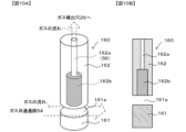
- an insulating sleeve 160 including a lower cylindrical body 161 and an upper cylindrical body 162 that are independent of each other may be used instead of the insulating sleeve 60.
- FIG. 10A is a perspective view of the insulating sleeve 160
- FIG. 10B is a longitudinal sectional view thereof.
- the lower cylindrical body 161 and the upper cylindrical body 162 are made of an electrically insulating material (for example, the same material as the ceramic plate 20).
- the lower cylindrical body 161 is a solid cylindrical body.
- a gap is formed between the upper surface of the lower cylindrical body 161 and the lower surface of the upper cylindrical body 162. This gap is the first communication hole 161a that constitutes a part of the gas common passage 54.
- the upper cylindrical body 162 has a second communication hole 162a.
- the second communication hole 162a communicates with the gas ejection hole 26, and forms a gas outflow passage 56 together with the gas ejection hole 26.
- the second communication hole 162a includes a porous cylindrical body 162b in a section (large diameter storage part) from the lower surface of the upper cylindrical body 162 to a predetermined height above. The height of the storage section is the same as the height of the porous columnar body 162b.
- the porous cylindrical body 162b is press-fitted into the storage part, and gas can flow in the vertical direction.
- the porous cylindrical body 162b is made of an electrically insulating material (for example, the same material as the ceramic plate 20).
- a plurality of such insulating sleeves 160 are provided in the gas common passage 54, and the closer the insulating sleeves 160 are to the gas inflow passage 52 (the ones upstream), the longer the vertical length of the storage section and the porous cylindrical body 162b (that is, the gas flow resistance (larger), and the farther from the gas inflow passage 52 (downstream), the shorter the vertical length of the storage section and porous columnar body 162b (that is, the smaller the gas flow resistance).
- the same effects as in the embodiment described above can be achieved.
- the insulating sleeve 160 is composed of two independent members, the replacement work is a little more complicated than the insulating sleeve 60.
- the gas passage resistance may be adjusted by the density of the porous cylindrical body 162b.
- the gas passage resistance is adjusted by the length of the spiral portion 67 provided in the second communication hole 66 of the insulating sleeve 60, but the present invention is not limited thereto.
- the gas passage resistance may be adjusted by the passage cross-sectional area (for example, hole diameter) of the spiral portion 67.
- the spiral portion 67 of the second communicating hole 66 of the insulating sleeve 60 is eliminated and the spiral portion 67 is formed straight, and a needle valve is attached to the intersection of the first communicating hole 64 and the second communicating hole 66.
- the gas passage resistance may be adjusted by adjusting the cross-sectional area of the passage from the first communication hole 64 to the second communication hole 66.
- the first communication holes 64 of the insulating sleeve 60 are provided radially in three directions centering on the second communication hole 66 in plan view, but may be provided radially in four or more directions.
- FIG. 11 is an explanatory diagram of an example in which the first communication holes 264 are provided radially in four directions centering on the second communication hole 66 in plan view.
- the four first communication holes 264 are provided at equal angles (almost equal angles). Even in this case, there is no need to consider the orientation of the first communication hole 64 when attaching the insulating sleeve 60 to the base plate through hole 31.
- a linear first communication hole 364 may be provided that intersects the second communication hole 66 in plan view.
- the lower part of the insulating sleeve 60 is sealed by adhering to the large diameter portion 31d of the base plate through hole 31 using the resin adhesive layer 38, but the present invention is not particularly limited to this.
- a seal ring 39 is disposed between the insulating sleeve 60 and the large diameter portion 31d of the base plate through hole 31 to prevent gas from leaking from the outer periphery of the insulating sleeve 60 to the outside. It's okay.
- the seal ring 39 may be made of metal or resin.
- the same reference numerals are attached to the same components as in the embodiment described above.
- a gap through which gas can pass was provided between the sleeve insertion portion 54a of the gas common passage 54 and the insulating sleeve 60, but the gap is not limited thereto.
- the sleeve insertion portion 54a may not be formed in the gas common passage 54, and the outer diameter of the insulating sleeve 60 may be made smaller than the width of the gas common passage 54. Even in this case, the same effects as in the embodiment described above can be achieved.
- the arc-shaped sleeve insertion portion 54a may be omitted, and the outer diameter of the insulating sleeve 60 may match (or almost match) the width of the gas common passage 54.
- the spiral portion 67 was provided in the second communication hole 66 that constitutes a part of the gas circulation portion 56, but a zigzag portion was provided instead of the spiral portion 67, and the length of the zigzag portion, etc. Gas passage resistance may be adjusted.
- the gas passage resistance is adjusted in the second communication hole 66 in the base plate 30 in the gas outflow passage 56, but the present invention is not particularly limited thereto.
- the gas passage resistance may be adjusted using the gas ejection holes 26 in the ceramic plate 20 in the gas outflow passage 56.
- the gas common passage 54 is provided in the base plate 30, but the gas common passage may be provided in the ceramic plate 20. In that case, gas passage resistance is adjusted in the path from the gas common path to the wafer mounting surface.
- the number of gas inflow passages 52 is one for the gas common passage 54, but the number may be smaller than the number of gas outflow passages 56 provided in the gas common passage 54.
- the one closest to the gas outflow passage 56 is The determination may be made using the distance to the gas inflow passage 52.
- the gas common passage 54 has a C-shape in plan view, but is not particularly limited to this.
- it may have a spiral shape in plan view.
- a plurality of gas common passages 54 having a C-shape in plan view may be provided along a plurality of concentric circles.
- the electrostatic electrode 22 and the heater electrode 23 are built into the ceramic plate 20, but the present invention is not particularly limited thereto.
- the ceramic plate 20 may include only one of the electrostatic electrode 22 and the heater electrode 23.
- the heater electrodes 23 may be built-in in two or more stages in the thickness direction.
- lift pin holes may be provided that penetrate the wafer mounting table 10.
- the lift pin hole is a hole through which a lift pin for moving the wafer W up and down with respect to the wafer mounting surface 21 is inserted.
- Lift pin holes are provided at three locations when the wafer W is supported by, for example, three lift pins.
- the ceramic plate 20 was produced by hot press firing a ceramic powder compact, but the compact at that time may be produced by laminating a plurality of tape compacts, or by molding. It may be produced by a casting method or by compacting ceramic powder.
- the member for semiconductor manufacturing equipment of the present invention can be used, for example, in the field of processing wafers with plasma or the like.
Landscapes
- Container, Conveyance, Adherence, Positioning, Of Wafer (AREA)
- Chemical Vapour Deposition (AREA)
- Drying Of Semiconductors (AREA)
Abstract
Description
ウエハ載置面を備えた半導体製造装置用部材であって、
前記ウエハ載置面に開口する複数のガス流出通路と、
前記半導体製造装置用部材の内部に設けられ、前記複数のガス流出通路に連通するガス共通通路と、
前記半導体製造装置用部材のうち前記ウエハ載置面とは反対側の面から前記ガス共通通路に連通し、前記ガス共通通路に連通する前記ガス流出通路の数よりも少ない数のガス流入通路と、
を備え、
前記複数のガス流出通路のうち前記ガス流入通路に近いものは、前記ガス流入通路から遠いものに比べてガス通過抵抗が大きい、
ものである。
Claims (10)
- ウエハ載置面を備えた半導体製造装置用部材であって、
前記ウエハ載置面に開口する複数のガス流出通路と、
前記半導体製造装置用部材の内部に設けられ、前記複数のガス流出通路に連通するガス共通通路と、
前記半導体製造装置用部材のうち前記ウエハ載置面とは反対側の面から前記ガス共通通路に連通し、前記ガス共通通路に連通する前記ガス流出通路の数よりも少ない数のガス流入通路と、
を備え、
前記複数のガス流出通路のうち前記ガス流入通路に近いものは、前記ガス流入通路から遠いものに比べてガス通過抵抗が大きい、
半導体製造装置用部材。 - 前記ガス通過抵抗は、前記ガス流出通路に設けられた螺旋部の長さ又は断面積によって調整されているか、前記ガス流出通路に設けられた多孔質部の長さ又は密度によって調整されている、
請求項1に記載の半導体製造装置用部材。 - 請求項1又は2に記載の半導体製造装置用部材であって、
上面に前記ウエハ載置面を有し、電極を内蔵するセラミックプレートと、
前記セラミックプレートの下面に設けられた導電性のベースプレートと、
を備え、
前記ガス共通通路及び前記ガス流入通路は、前記ベースプレートに設けられ、
前記ガス流出通路は、前記ガス共通通路から前記ウエハ載置面に至るように前記ベースプレート及び前記セラミックプレートに設けられている、
半導体製造装置用部材。 - 前記ベースプレートは、冷媒流路を有し、
前記ガス共通通路は、前記ベースプレートのうち前記冷媒流路の下方に設けられ、
前記ガス通過抵抗は、前記ガス流出通路のうち前記ガス共通通路から前記ベースプレートの上面に至るまでの部分で調整されている、
請求項3に記載の半導体製造装置用部材。 - 前記ベースプレートは、前記ベースプレートを上下方向に貫通するベースプレート貫通穴内に絶縁スリーブを有し、
前記絶縁スリーブは、前記ガス共通通路の一部を構成する第1連通穴と、前記第1連通穴から前記絶縁スリーブの上面に至るように設けられ、前記ガス流出通路の一部を構成する第2連通穴と、を有し、
前記ガス通過抵抗は、前記絶縁スリーブの前記第2連通穴で調整されている、
請求項3に記載の半導体製造装置用部材。 - 前記絶縁スリーブは、分離不能な1つの部材である、
請求項5に記載の半導体製造装置用部材。 - 前記絶縁スリーブの前記第1連通穴は、平面視で前記第2連通穴を中心として少なくとも3つの方向に放射状に設けられている、
請求項5に記載の半導体製造装置用部材。 - 前記絶縁スリーブの外径は、前記ガス共通通路の幅よりも小さい、
請求項5に記載の半導体製造装置用部材。 - 前記セラミックプレートと前記ベースプレートとは、導電性接合層によって接合され、
前記絶縁スリーブは、前記導電性接合層に挿入されている、
請求項5に記載の半導体製造装置用部材。 - 前記絶縁スリーブの上面は、上部樹脂接着層を介して前記セラミックプレートと接着され、前記絶縁スリーブの下部は、下部樹脂接着層又はシール材を介して前記ベースプレートに取り付けられている、
請求項5に記載の半導体製造装置用部材。
Priority Applications (6)
| Application Number | Priority Date | Filing Date | Title |
|---|---|---|---|
| KR1020237009185A KR102698667B1 (ko) | 2022-06-30 | 2022-06-30 | 반도체 제조 장치용 부재 |
| CN202280006001.XA CN119365971A (zh) | 2022-06-30 | 2022-06-30 | 半导体制造装置用部件 |
| PCT/JP2022/026285 WO2024004147A1 (ja) | 2022-06-30 | 2022-06-30 | 半導体製造装置用部材 |
| JP2023515572A JP7499408B2 (ja) | 2022-06-30 | 2022-06-30 | 半導体製造装置用部材 |
| US18/180,929 US12538755B2 (en) | 2022-06-30 | 2023-03-09 | Member for semiconductor manufacturing apparatus |
| TW112124221A TW202410272A (zh) | 2022-06-30 | 2023-06-29 | 半導體製造裝置用構件 |
Applications Claiming Priority (1)
| Application Number | Priority Date | Filing Date | Title |
|---|---|---|---|
| PCT/JP2022/026285 WO2024004147A1 (ja) | 2022-06-30 | 2022-06-30 | 半導体製造装置用部材 |
Related Child Applications (1)
| Application Number | Title | Priority Date | Filing Date |
|---|---|---|---|
| US18/180,929 Continuation US12538755B2 (en) | 2022-06-30 | 2023-03-09 | Member for semiconductor manufacturing apparatus |
Publications (1)
| Publication Number | Publication Date |
|---|---|
| WO2024004147A1 true WO2024004147A1 (ja) | 2024-01-04 |
Family
ID=89382452
Family Applications (1)
| Application Number | Title | Priority Date | Filing Date |
|---|---|---|---|
| PCT/JP2022/026285 Ceased WO2024004147A1 (ja) | 2022-06-30 | 2022-06-30 | 半導体製造装置用部材 |
Country Status (6)
| Country | Link |
|---|---|
| US (1) | US12538755B2 (ja) |
| JP (1) | JP7499408B2 (ja) |
| KR (1) | KR102698667B1 (ja) |
| CN (1) | CN119365971A (ja) |
| TW (1) | TW202410272A (ja) |
| WO (1) | WO2024004147A1 (ja) |
Cited By (2)
| Publication number | Priority date | Publication date | Assignee | Title |
|---|---|---|---|---|
| JP2024088883A (ja) * | 2022-12-21 | 2024-07-03 | 日本碍子株式会社 | プラグ、プラグ製造方法及び半導体製造装置用部材 |
| JP7514990B1 (ja) | 2023-09-11 | 2024-07-11 | 日本特殊陶業株式会社 | 保持装置 |
Families Citing this family (1)
| Publication number | Priority date | Publication date | Assignee | Title |
|---|---|---|---|---|
| WO2024069816A1 (ja) * | 2022-09-28 | 2024-04-04 | 日本碍子株式会社 | 静電チャックアセンブリ |
Citations (6)
| Publication number | Priority date | Publication date | Assignee | Title |
|---|---|---|---|---|
| US6024631A (en) * | 1996-11-26 | 2000-02-15 | Micron Technology, Inc. | Method and apparatus to hold integrated circuit chips onto a chuck and to simultaneously remove multiple integrated circuit chips from a cutting chuck |
| JP2009158829A (ja) * | 2007-12-27 | 2009-07-16 | Shinko Electric Ind Co Ltd | 静電チャック及び基板温調固定装置 |
| JP3182120U (ja) * | 2012-12-26 | 2013-03-07 | 日本碍子株式会社 | セラミックヒーター |
| JP2014049685A (ja) * | 2012-09-03 | 2014-03-17 | Ngk Spark Plug Co Ltd | 半導体製造用部品 |
| JP2019117861A (ja) * | 2017-12-27 | 2019-07-18 | 株式会社日立ハイテクノロジーズ | ウエハ処理方法およびウエハ処理装置 |
| JP2020057786A (ja) * | 2018-09-28 | 2020-04-09 | 日本碍子株式会社 | 半導体製造装置用部材 |
Family Cites Families (8)
| Publication number | Priority date | Publication date | Assignee | Title |
|---|---|---|---|---|
| JP3181501B2 (ja) * | 1995-10-31 | 2001-07-03 | 東京エレクトロン株式会社 | 処理装置および処理方法 |
| US8540819B2 (en) * | 2008-03-21 | 2013-09-24 | Ngk Insulators, Ltd. | Ceramic heater |
| JP6678458B2 (ja) | 2016-01-07 | 2020-04-08 | 日本特殊陶業株式会社 | 静電チャック |
| TWI677593B (zh) | 2016-04-01 | 2019-11-21 | 美商應用材料股份有限公司 | 用於提供均勻流動的氣體的設備及方法 |
| KR101987451B1 (ko) | 2017-10-18 | 2019-06-11 | 세메스 주식회사 | 기판 지지부재 및 이를 포함하는 기판 처리 장치 |
| KR102329167B1 (ko) * | 2017-11-20 | 2021-11-22 | 주식회사 원익아이피에스 | 기판 지지 어셈블리 및 이를 포함하는 기판 처리 장치 |
| JP7144603B2 (ja) | 2019-04-25 | 2022-09-29 | 日本碍子株式会社 | 3次元焼成体の製法 |
| US12165897B2 (en) * | 2019-11-25 | 2024-12-10 | Kyocera Corporation | Workpiece holding tool |
-
2022
- 2022-06-30 KR KR1020237009185A patent/KR102698667B1/ko active Active
- 2022-06-30 WO PCT/JP2022/026285 patent/WO2024004147A1/ja not_active Ceased
- 2022-06-30 CN CN202280006001.XA patent/CN119365971A/zh active Pending
- 2022-06-30 JP JP2023515572A patent/JP7499408B2/ja active Active
-
2023
- 2023-03-09 US US18/180,929 patent/US12538755B2/en active Active
- 2023-06-29 TW TW112124221A patent/TW202410272A/zh unknown
Patent Citations (6)
| Publication number | Priority date | Publication date | Assignee | Title |
|---|---|---|---|---|
| US6024631A (en) * | 1996-11-26 | 2000-02-15 | Micron Technology, Inc. | Method and apparatus to hold integrated circuit chips onto a chuck and to simultaneously remove multiple integrated circuit chips from a cutting chuck |
| JP2009158829A (ja) * | 2007-12-27 | 2009-07-16 | Shinko Electric Ind Co Ltd | 静電チャック及び基板温調固定装置 |
| JP2014049685A (ja) * | 2012-09-03 | 2014-03-17 | Ngk Spark Plug Co Ltd | 半導体製造用部品 |
| JP3182120U (ja) * | 2012-12-26 | 2013-03-07 | 日本碍子株式会社 | セラミックヒーター |
| JP2019117861A (ja) * | 2017-12-27 | 2019-07-18 | 株式会社日立ハイテクノロジーズ | ウエハ処理方法およびウエハ処理装置 |
| JP2020057786A (ja) * | 2018-09-28 | 2020-04-09 | 日本碍子株式会社 | 半導体製造装置用部材 |
Cited By (4)
| Publication number | Priority date | Publication date | Assignee | Title |
|---|---|---|---|---|
| JP2024088883A (ja) * | 2022-12-21 | 2024-07-03 | 日本碍子株式会社 | プラグ、プラグ製造方法及び半導体製造装置用部材 |
| JP7764356B2 (ja) | 2022-12-21 | 2025-11-05 | 日本碍子株式会社 | プラグ、プラグ製造方法及び半導体製造装置用部材 |
| JP7514990B1 (ja) | 2023-09-11 | 2024-07-11 | 日本特殊陶業株式会社 | 保持装置 |
| JP2025040093A (ja) * | 2023-09-11 | 2025-03-24 | 日本特殊陶業株式会社 | 保持装置 |
Also Published As
| Publication number | Publication date |
|---|---|
| US12538755B2 (en) | 2026-01-27 |
| KR102698667B1 (ko) | 2024-08-23 |
| TW202410272A (zh) | 2024-03-01 |
| CN119365971A (zh) | 2025-01-24 |
| US20240006226A1 (en) | 2024-01-04 |
| JP7499408B2 (ja) | 2024-06-13 |
| JPWO2024004147A1 (ja) | 2024-01-04 |
| KR20240003743A (ko) | 2024-01-09 |
Similar Documents
| Publication | Publication Date | Title |
|---|---|---|
| JP7499408B2 (ja) | 半導体製造装置用部材 | |
| KR102772087B1 (ko) | 웨이퍼 배치대 | |
| KR102755203B1 (ko) | 웨이퍼 배치대 | |
| JP7764356B2 (ja) | プラグ、プラグ製造方法及び半導体製造装置用部材 | |
| JP7364822B1 (ja) | ウエハ載置台 | |
| US12444586B2 (en) | Wafer placement table | |
| KR102908868B1 (ko) | 웨이퍼 배치대 | |
| TW202314928A (zh) | 晶圓放置座 | |
| CN116190186A (zh) | 晶片载放台 | |
| JP7499955B2 (ja) | 半導体製造装置用部材 | |
| KR102717444B1 (ko) | 웨이퍼 배치대 및 그것을 이용한 반도체 제조 장치용 부재 | |
| JP2025109922A (ja) | ウエハ載置台 | |
| CN120981907A (zh) | 晶片载放台 | |
| JP7744328B2 (ja) | 半導体製造装置用部材、プラグ及びプラグ製造方法 | |
| CN116564779A (zh) | 晶片载放台及采用了该晶片载放台的半导体制造装置用部件 |
Legal Events
| Date | Code | Title | Description |
|---|---|---|---|
| WWE | Wipo information: entry into national phase |
Ref document number: 202280006001.X Country of ref document: CN |
|
| ENP | Entry into the national phase |
Ref document number: 2023515572 Country of ref document: JP Kind code of ref document: A |
|
| 121 | Ep: the epo has been informed by wipo that ep was designated in this application |
Ref document number: 22949420 Country of ref document: EP Kind code of ref document: A1 |
|
| WWP | Wipo information: published in national office |
Ref document number: 202280006001.X Country of ref document: CN |
|
| NENP | Non-entry into the national phase |
Ref country code: DE |
|
| 122 | Ep: pct application non-entry in european phase |
Ref document number: 22949420 Country of ref document: EP Kind code of ref document: A1 |