WO2023282138A1 - Organic metal complex, and organic light-emitting element, display device, imaging device, electronic equipment, lighting device and mobile object each containing same - Google Patents
Organic metal complex, and organic light-emitting element, display device, imaging device, electronic equipment, lighting device and mobile object each containing same Download PDFInfo
- Publication number
- WO2023282138A1 WO2023282138A1 PCT/JP2022/025913 JP2022025913W WO2023282138A1 WO 2023282138 A1 WO2023282138 A1 WO 2023282138A1 JP 2022025913 W JP2022025913 W JP 2022025913W WO 2023282138 A1 WO2023282138 A1 WO 2023282138A1
- Authority
- WO
- WIPO (PCT)
- Prior art keywords
- light
- layer
- organic light
- group
- electrode
- Prior art date
Links
- 238000003384 imaging method Methods 0.000 title claims description 38
- 150000004696 coordination complex Chemical class 0.000 title abstract description 4
- 125000000217 alkyl group Chemical group 0.000 claims abstract description 49
- 125000004432 carbon atom Chemical group C* 0.000 claims abstract description 31
- 125000004435 hydrogen atom Chemical group [H]* 0.000 claims abstract description 29
- 125000001424 substituent group Chemical group 0.000 claims abstract description 25
- 229910052751 metal Inorganic materials 0.000 claims abstract description 19
- 239000002184 metal Substances 0.000 claims abstract description 19
- 229910052741 iridium Inorganic materials 0.000 claims abstract description 10
- 229910052763 palladium Inorganic materials 0.000 claims abstract description 9
- 125000004429 atom Chemical group 0.000 claims abstract description 8
- 229910052697 platinum Inorganic materials 0.000 claims abstract description 8
- 229910052707 ruthenium Inorganic materials 0.000 claims abstract description 7
- 150000001875 compounds Chemical class 0.000 claims description 79
- 150000002894 organic compounds Chemical class 0.000 claims description 58
- 125000002524 organometallic group Chemical group 0.000 claims description 37
- 125000000753 cycloalkyl group Chemical group 0.000 claims description 14
- 125000003118 aryl group Chemical group 0.000 claims description 13
- 125000005843 halogen group Chemical group 0.000 claims description 12
- 125000004093 cyano group Chemical group *C#N 0.000 claims description 10
- 125000000449 nitro group Chemical group [O-][N+](*)=O 0.000 claims description 10
- 230000003287 optical effect Effects 0.000 claims description 10
- 125000004665 trialkylsilyl group Chemical group 0.000 claims description 10
- 125000001997 phenyl group Chemical group [H]C1=C([H])C([H])=C(*)C([H])=C1[H] 0.000 claims description 7
- 238000004891 communication Methods 0.000 claims description 5
- 238000009792 diffusion process Methods 0.000 claims description 4
- 239000012788 optical film Substances 0.000 claims description 3
- 125000000999 tert-butyl group Chemical group [H]C([H])([H])C(*)(C([H])([H])[H])C([H])([H])[H] 0.000 claims description 2
- 239000010410 layer Substances 0.000 description 179
- 239000000463 material Substances 0.000 description 46
- 239000000758 substrate Substances 0.000 description 45
- 238000000034 method Methods 0.000 description 30
- 230000000052 comparative effect Effects 0.000 description 28
- -1 specifically Chemical group 0.000 description 27
- 230000015572 biosynthetic process Effects 0.000 description 24
- 239000010408 film Substances 0.000 description 24
- 238000003786 synthesis reaction Methods 0.000 description 21
- 238000004128 high performance liquid chromatography Methods 0.000 description 18
- 239000011241 protective layer Substances 0.000 description 18
- 238000010586 diagram Methods 0.000 description 17
- 238000002347 injection Methods 0.000 description 15
- 239000007924 injection Substances 0.000 description 15
- 238000000859 sublimation Methods 0.000 description 12
- 230000008022 sublimation Effects 0.000 description 12
- 230000000903 blocking effect Effects 0.000 description 11
- 238000000576 coating method Methods 0.000 description 11
- 239000011521 glass Substances 0.000 description 11
- 238000004458 analytical method Methods 0.000 description 10
- 210000005252 bulbus oculi Anatomy 0.000 description 10
- KFZMGEQAYNKOFK-UHFFFAOYSA-N Isopropanol Chemical compound CC(C)O KFZMGEQAYNKOFK-UHFFFAOYSA-N 0.000 description 9
- 239000000470 constituent Substances 0.000 description 9
- 239000000203 mixture Substances 0.000 description 9
- 239000011347 resin Substances 0.000 description 9
- 229920005989 resin Polymers 0.000 description 9
- 230000005525 hole transport Effects 0.000 description 8
- 230000007423 decrease Effects 0.000 description 7
- 239000012299 nitrogen atmosphere Substances 0.000 description 7
- KDLHZDBZIXYQEI-UHFFFAOYSA-N palladium Substances [Pd] KDLHZDBZIXYQEI-UHFFFAOYSA-N 0.000 description 7
- 239000004984 smart glass Substances 0.000 description 7
- BQCADISMDOOEFD-UHFFFAOYSA-N Silver Chemical compound [Ag] BQCADISMDOOEFD-UHFFFAOYSA-N 0.000 description 6
- YXFVVABEGXRONW-UHFFFAOYSA-N Toluene Chemical compound CC1=CC=CC=C1 YXFVVABEGXRONW-UHFFFAOYSA-N 0.000 description 6
- 238000001514 detection method Methods 0.000 description 6
- 239000003446 ligand Substances 0.000 description 6
- PQXKHYXIUOZZFA-UHFFFAOYSA-M lithium fluoride Chemical compound [Li+].[F-] PQXKHYXIUOZZFA-UHFFFAOYSA-M 0.000 description 6
- 229910052709 silver Inorganic materials 0.000 description 6
- 239000004332 silver Substances 0.000 description 6
- 239000002356 single layer Substances 0.000 description 6
- 239000004925 Acrylic resin Substances 0.000 description 5
- 229920000178 Acrylic resin Polymers 0.000 description 5
- 238000001035 drying Methods 0.000 description 5
- 125000001153 fluoro group Chemical group F* 0.000 description 5
- 150000002739 metals Chemical class 0.000 description 5
- BASFCYQUMIYNBI-UHFFFAOYSA-N platinum Substances [Pt] BASFCYQUMIYNBI-UHFFFAOYSA-N 0.000 description 5
- 239000002904 solvent Substances 0.000 description 5
- 238000004528 spin coating Methods 0.000 description 5
- 239000010409 thin film Substances 0.000 description 5
- XLYOFNOQVPJJNP-UHFFFAOYSA-N water Substances O XLYOFNOQVPJJNP-UHFFFAOYSA-N 0.000 description 5
- XUIMIQQOPSSXEZ-UHFFFAOYSA-N Silicon Chemical compound [Si] XUIMIQQOPSSXEZ-UHFFFAOYSA-N 0.000 description 4
- XLOMVQKBTHCTTD-UHFFFAOYSA-N Zinc monoxide Chemical compound [Zn]=O XLOMVQKBTHCTTD-UHFFFAOYSA-N 0.000 description 4
- 229910045601 alloy Inorganic materials 0.000 description 4
- 239000000956 alloy Substances 0.000 description 4
- 229910052782 aluminium Inorganic materials 0.000 description 4
- XAGFODPZIPBFFR-UHFFFAOYSA-N aluminium Chemical compound [Al] XAGFODPZIPBFFR-UHFFFAOYSA-N 0.000 description 4
- 239000007864 aqueous solution Substances 0.000 description 4
- 239000011248 coating agent Substances 0.000 description 4
- 239000003086 colorant Substances 0.000 description 4
- 239000002019 doping agent Substances 0.000 description 4
- 125000003983 fluorenyl group Chemical group C1(=CC=CC=2C3=CC=CC=C3CC12)* 0.000 description 4
- 229910052731 fluorine Inorganic materials 0.000 description 4
- 239000007788 liquid Substances 0.000 description 4
- 229920003227 poly(N-vinyl carbazole) Polymers 0.000 description 4
- 230000008569 process Effects 0.000 description 4
- 230000001681 protective effect Effects 0.000 description 4
- 239000004065 semiconductor Substances 0.000 description 4
- 229910052710 silicon Inorganic materials 0.000 description 4
- 239000010703 silicon Substances 0.000 description 4
- 238000004544 sputter deposition Methods 0.000 description 4
- 230000000007 visual effect Effects 0.000 description 4
- VQGHOUODWALEFC-UHFFFAOYSA-N 2-phenylpyridine Chemical compound C1=CC=CC=C1C1=CC=CC=N1 VQGHOUODWALEFC-UHFFFAOYSA-N 0.000 description 3
- UGGNULHQVUWRGQ-UHFFFAOYSA-N 4-tert-butyl-2-chloropyridine Chemical compound CC(C)(C)C1=CC=NC(Cl)=C1 UGGNULHQVUWRGQ-UHFFFAOYSA-N 0.000 description 3
- LYCAIKOWRPUZTN-UHFFFAOYSA-N Ethylene glycol Chemical compound OCCO LYCAIKOWRPUZTN-UHFFFAOYSA-N 0.000 description 3
- OKKJLVBELUTLKV-UHFFFAOYSA-N Methanol Chemical compound OC OKKJLVBELUTLKV-UHFFFAOYSA-N 0.000 description 3
- 229910052581 Si3N4 Inorganic materials 0.000 description 3
- 239000012298 atmosphere Substances 0.000 description 3
- 239000002585 base Substances 0.000 description 3
- 238000005452 bending Methods 0.000 description 3
- 239000011230 binding agent Substances 0.000 description 3
- 229920001577 copolymer Polymers 0.000 description 3
- 230000006866 deterioration Effects 0.000 description 3
- ZXHUJRZYLRVVNP-UHFFFAOYSA-N dibenzofuran-4-ylboronic acid Chemical compound C12=CC=CC=C2OC2=C1C=CC=C2B(O)O ZXHUJRZYLRVVNP-UHFFFAOYSA-N 0.000 description 3
- 238000010438 heat treatment Methods 0.000 description 3
- 229910052739 hydrogen Inorganic materials 0.000 description 3
- AMGQUBHHOARCQH-UHFFFAOYSA-N indium;oxotin Chemical compound [In].[Sn]=O AMGQUBHHOARCQH-UHFFFAOYSA-N 0.000 description 3
- 238000007641 inkjet printing Methods 0.000 description 3
- 239000011229 interlayer Substances 0.000 description 3
- GKOZUEZYRPOHIO-UHFFFAOYSA-N iridium atom Chemical compound [Ir] GKOZUEZYRPOHIO-UHFFFAOYSA-N 0.000 description 3
- 239000011159 matrix material Substances 0.000 description 3
- 229910021421 monocrystalline silicon Inorganic materials 0.000 description 3
- 230000007935 neutral effect Effects 0.000 description 3
- 125000004430 oxygen atom Chemical group O* 0.000 description 3
- 230000035515 penetration Effects 0.000 description 3
- 239000004417 polycarbonate Substances 0.000 description 3
- 229920001721 polyimide Polymers 0.000 description 3
- 229920000642 polymer Chemical class 0.000 description 3
- 238000007639 printing Methods 0.000 description 3
- HQVNEWCFYHHQES-UHFFFAOYSA-N silicon nitride Chemical compound N12[Si]34N5[Si]62N3[Si]51N64 HQVNEWCFYHHQES-UHFFFAOYSA-N 0.000 description 3
- 238000001771 vacuum deposition Methods 0.000 description 3
- YVTHLONGBIQYBO-UHFFFAOYSA-N zinc indium(3+) oxygen(2-) Chemical compound [O--].[Zn++].[In+3] YVTHLONGBIQYBO-UHFFFAOYSA-N 0.000 description 3
- ZCYVEMRRCGMTRW-UHFFFAOYSA-N 7553-56-2 Chemical group [I] ZCYVEMRRCGMTRW-UHFFFAOYSA-N 0.000 description 2
- XKRFYHLGVUSROY-UHFFFAOYSA-N Argon Chemical compound [Ar] XKRFYHLGVUSROY-UHFFFAOYSA-N 0.000 description 2
- IJGRMHOSHXDMSA-UHFFFAOYSA-N Atomic nitrogen Chemical compound N#N IJGRMHOSHXDMSA-UHFFFAOYSA-N 0.000 description 2
- WKBOTKDWSSQWDR-UHFFFAOYSA-N Bromine atom Chemical compound [Br] WKBOTKDWSSQWDR-UHFFFAOYSA-N 0.000 description 2
- HEDRZPFGACZZDS-UHFFFAOYSA-N Chloroform Chemical compound ClC(Cl)Cl HEDRZPFGACZZDS-UHFFFAOYSA-N 0.000 description 2
- VYZAMTAEIAYCRO-UHFFFAOYSA-N Chromium Chemical compound [Cr] VYZAMTAEIAYCRO-UHFFFAOYSA-N 0.000 description 2
- 229940126062 Compound A Drugs 0.000 description 2
- RGSFGYAAUTVSQA-UHFFFAOYSA-N Cyclopentane Chemical compound C1CCCC1 RGSFGYAAUTVSQA-UHFFFAOYSA-N 0.000 description 2
- LFQSCWFLJHTTHZ-UHFFFAOYSA-N Ethanol Chemical compound CCO LFQSCWFLJHTTHZ-UHFFFAOYSA-N 0.000 description 2
- NLDMNSXOCDLTTB-UHFFFAOYSA-N Heterophylliin A Natural products O1C2COC(=O)C3=CC(O)=C(O)C(O)=C3C3=C(O)C(O)=C(O)C=C3C(=O)OC2C(OC(=O)C=2C=C(O)C(O)=C(O)C=2)C(O)C1OC(=O)C1=CC(O)=C(O)C(O)=C1 NLDMNSXOCDLTTB-UHFFFAOYSA-N 0.000 description 2
- CSNNHWWHGAXBCP-UHFFFAOYSA-L Magnesium sulfate Chemical compound [Mg+2].[O-][S+2]([O-])([O-])[O-] CSNNHWWHGAXBCP-UHFFFAOYSA-L 0.000 description 2
- 238000005481 NMR spectroscopy Methods 0.000 description 2
- PXHVJJICTQNCMI-UHFFFAOYSA-N Nickel Chemical compound [Ni] PXHVJJICTQNCMI-UHFFFAOYSA-N 0.000 description 2
- 229920001609 Poly(3,4-ethylenedioxythiophene) Polymers 0.000 description 2
- 229920000265 Polyparaphenylene Polymers 0.000 description 2
- JUJWROOIHBZHMG-UHFFFAOYSA-N Pyridine Chemical compound C1=CC=NC=C1 JUJWROOIHBZHMG-UHFFFAOYSA-N 0.000 description 2
- CDBYLPFSWZWCQE-UHFFFAOYSA-L Sodium Carbonate Chemical compound [Na+].[Na+].[O-]C([O-])=O CDBYLPFSWZWCQE-UHFFFAOYSA-L 0.000 description 2
- RTAQQCXQSZGOHL-UHFFFAOYSA-N Titanium Chemical compound [Ti] RTAQQCXQSZGOHL-UHFFFAOYSA-N 0.000 description 2
- 229920001807 Urea-formaldehyde Polymers 0.000 description 2
- 229920000122 acrylonitrile butadiene styrene Polymers 0.000 description 2
- 239000000853 adhesive Substances 0.000 description 2
- 230000001070 adhesive effect Effects 0.000 description 2
- 230000002776 aggregation Effects 0.000 description 2
- 238000004220 aggregation Methods 0.000 description 2
- 229910052783 alkali metal Inorganic materials 0.000 description 2
- 150000001340 alkali metals Chemical class 0.000 description 2
- 238000000137 annealing Methods 0.000 description 2
- 150000001454 anthracenes Chemical class 0.000 description 2
- 238000007611 bar coating method Methods 0.000 description 2
- 125000002619 bicyclic group Chemical group 0.000 description 2
- 239000003990 capacitor Substances 0.000 description 2
- 125000000609 carbazolyl group Chemical group C1(=CC=CC=2C3=CC=CC=C3NC12)* 0.000 description 2
- 229910052799 carbon Inorganic materials 0.000 description 2
- 238000006243 chemical reaction Methods 0.000 description 2
- 238000005229 chemical vapour deposition Methods 0.000 description 2
- 229910052801 chlorine Inorganic materials 0.000 description 2
- MVPPADPHJFYWMZ-UHFFFAOYSA-N chlorobenzene Chemical compound ClC1=CC=CC=C1 MVPPADPHJFYWMZ-UHFFFAOYSA-N 0.000 description 2
- 239000011651 chromium Substances 0.000 description 2
- 229910052804 chromium Inorganic materials 0.000 description 2
- 229920001940 conductive polymer Polymers 0.000 description 2
- 238000002425 crystallisation Methods 0.000 description 2
- 230000008025 crystallization Effects 0.000 description 2
- 238000000151 deposition Methods 0.000 description 2
- 230000002542 deteriorative effect Effects 0.000 description 2
- TXCDCPKCNAJMEE-UHFFFAOYSA-N dibenzofuran Chemical group C1=CC=C2C3=CC=CC=C3OC2=C1 TXCDCPKCNAJMEE-UHFFFAOYSA-N 0.000 description 2
- ZUOUZKKEUPVFJK-UHFFFAOYSA-N diphenyl Chemical compound C1=CC=CC=C1C1=CC=CC=C1 ZUOUZKKEUPVFJK-UHFFFAOYSA-N 0.000 description 2
- 230000007613 environmental effect Effects 0.000 description 2
- 239000003822 epoxy resin Substances 0.000 description 2
- 238000007756 gravure coating Methods 0.000 description 2
- 238000005286 illumination Methods 0.000 description 2
- 229910003437 indium oxide Inorganic materials 0.000 description 2
- 230000010365 information processing Effects 0.000 description 2
- 239000004973 liquid crystal related substance Substances 0.000 description 2
- 238000004519 manufacturing process Methods 0.000 description 2
- 229910044991 metal oxide Inorganic materials 0.000 description 2
- 125000001570 methylene group Chemical group [H]C([H])([*:1])[*:2] 0.000 description 2
- 150000002790 naphthalenes Chemical class 0.000 description 2
- 125000001624 naphthyl group Chemical group 0.000 description 2
- 239000012044 organic layer Substances 0.000 description 2
- 150000004866 oxadiazoles Chemical class 0.000 description 2
- 230000002093 peripheral effect Effects 0.000 description 2
- 239000005011 phenolic resin Substances 0.000 description 2
- 229920000553 poly(phenylenevinylene) Chemical class 0.000 description 2
- 229920000515 polycarbonate Polymers 0.000 description 2
- 229920005668 polycarbonate resin Polymers 0.000 description 2
- 239000004431 polycarbonate resin Substances 0.000 description 2
- 229920000647 polyepoxide Polymers 0.000 description 2
- 229920001225 polyester resin Polymers 0.000 description 2
- 239000004645 polyester resin Substances 0.000 description 2
- 239000009719 polyimide resin Substances 0.000 description 2
- 229920000123 polythiophene Polymers 0.000 description 2
- 238000012545 processing Methods 0.000 description 2
- 230000001179 pupillary effect Effects 0.000 description 2
- 238000001028 reflection method Methods 0.000 description 2
- VYPSYNLAJGMNEJ-UHFFFAOYSA-N silicon dioxide Inorganic materials O=[Si]=O VYPSYNLAJGMNEJ-UHFFFAOYSA-N 0.000 description 2
- 238000001179 sorption measurement Methods 0.000 description 2
- PJANXHGTPQOBST-UHFFFAOYSA-N stilbene Chemical class C=1C=CC=CC=1C=CC1=CC=CC=C1 PJANXHGTPQOBST-UHFFFAOYSA-N 0.000 description 2
- 229940042055 systemic antimycotics triazole derivative Drugs 0.000 description 2
- 239000010936 titanium Substances 0.000 description 2
- 229910052719 titanium Inorganic materials 0.000 description 2
- TVIVIEFSHFOWTE-UHFFFAOYSA-K tri(quinolin-8-yloxy)alumane Chemical compound [Al+3].C1=CN=C2C([O-])=CC=CC2=C1.C1=CN=C2C([O-])=CC=CC2=C1.C1=CN=C2C([O-])=CC=CC2=C1 TVIVIEFSHFOWTE-UHFFFAOYSA-K 0.000 description 2
- 150000003918 triazines Chemical class 0.000 description 2
- 239000010937 tungsten Substances 0.000 description 2
- WFKWXMTUELFFGS-UHFFFAOYSA-N tungsten Chemical compound [W] WFKWXMTUELFFGS-UHFFFAOYSA-N 0.000 description 2
- 229910052721 tungsten Inorganic materials 0.000 description 2
- 238000007740 vapor deposition Methods 0.000 description 2
- 235000012431 wafers Nutrition 0.000 description 2
- 239000011787 zinc oxide Substances 0.000 description 2
- 125000001637 1-naphthyl group Chemical group [H]C1=C([H])C([H])=C2C(*)=C([H])C([H])=C([H])C2=C1[H] 0.000 description 1
- MEKOFIRRDATTAG-UHFFFAOYSA-N 2,2,5,8-tetramethyl-3,4-dihydrochromen-6-ol Chemical compound C1CC(C)(C)OC2=C1C(C)=C(O)C=C2C MEKOFIRRDATTAG-UHFFFAOYSA-N 0.000 description 1
- MROTUXXYBNRZSG-UHFFFAOYSA-N 2-chloro-4-phenylpyridine Chemical compound C1=NC(Cl)=CC(C=2C=CC=CC=2)=C1 MROTUXXYBNRZSG-UHFFFAOYSA-N 0.000 description 1
- 125000002941 2-furyl group Chemical group O1C([*])=C([H])C([H])=C1[H] 0.000 description 1
- 125000001622 2-naphthyl group Chemical group [H]C1=C([H])C([H])=C2C([H])=C(*)C([H])=C([H])C2=C1[H] 0.000 description 1
- KXPQYZRZBNMOIN-UHFFFAOYSA-N 2-phenyl-1h-pyridine-2-carboxylic acid Chemical compound C=1C=CC=CC=1C1(C(=O)O)NC=CC=C1 KXPQYZRZBNMOIN-UHFFFAOYSA-N 0.000 description 1
- 125000004105 2-pyridyl group Chemical group N1=C([*])C([H])=C([H])C([H])=C1[H] 0.000 description 1
- 125000000175 2-thienyl group Chemical group S1C([*])=C([H])C([H])=C1[H] 0.000 description 1
- 125000004172 4-methoxyphenyl group Chemical group [H]C1=C([H])C(OC([H])([H])[H])=C([H])C([H])=C1* 0.000 description 1
- BPMBNLJJRKCCRT-UHFFFAOYSA-N 4-phenylbenzonitrile Chemical group C1=CC(C#N)=CC=C1C1=CC=CC=C1 BPMBNLJJRKCCRT-UHFFFAOYSA-N 0.000 description 1
- 229910001316 Ag alloy Inorganic materials 0.000 description 1
- 229910001148 Al-Li alloy Inorganic materials 0.000 description 1
- OYPRJOBELJOOCE-UHFFFAOYSA-N Calcium Chemical compound [Ca] OYPRJOBELJOOCE-UHFFFAOYSA-N 0.000 description 1
- ZAMOUSCENKQFHK-UHFFFAOYSA-N Chlorine atom Chemical compound [Cl] ZAMOUSCENKQFHK-UHFFFAOYSA-N 0.000 description 1
- RYGMFSIKBFXOCR-UHFFFAOYSA-N Copper Chemical compound [Cu] RYGMFSIKBFXOCR-UHFFFAOYSA-N 0.000 description 1
- XDTMQSROBMDMFD-UHFFFAOYSA-N Cyclohexane Chemical compound C1CCCCC1 XDTMQSROBMDMFD-UHFFFAOYSA-N 0.000 description 1
- 150000000918 Europium Chemical class 0.000 description 1
- PXGOKWXKJXAPGV-UHFFFAOYSA-N Fluorine Chemical compound FF PXGOKWXKJXAPGV-UHFFFAOYSA-N 0.000 description 1
- GYHNNYVSQQEPJS-UHFFFAOYSA-N Gallium Chemical compound [Ga] GYHNNYVSQQEPJS-UHFFFAOYSA-N 0.000 description 1
- WHXSMMKQMYFTQS-UHFFFAOYSA-N Lithium Chemical compound [Li] WHXSMMKQMYFTQS-UHFFFAOYSA-N 0.000 description 1
- ZOKXTWBITQBERF-UHFFFAOYSA-N Molybdenum Chemical compound [Mo] ZOKXTWBITQBERF-UHFFFAOYSA-N 0.000 description 1
- 240000007594 Oryza sativa Species 0.000 description 1
- 235000007164 Oryza sativa Nutrition 0.000 description 1
- 239000004642 Polyimide Substances 0.000 description 1
- NRCMAYZCPIVABH-UHFFFAOYSA-N Quinacridone Chemical class N1C2=CC=CC=C2C(=O)C2=C1C=C1C(=O)C3=CC=CC=C3NC1=C2 NRCMAYZCPIVABH-UHFFFAOYSA-N 0.000 description 1
- BUGBHKTXTAQXES-UHFFFAOYSA-N Selenium Chemical compound [Se] BUGBHKTXTAQXES-UHFFFAOYSA-N 0.000 description 1
- 235000002597 Solanum melongena Nutrition 0.000 description 1
- ATJFFYVFTNAWJD-UHFFFAOYSA-N Tin Chemical compound [Sn] ATJFFYVFTNAWJD-UHFFFAOYSA-N 0.000 description 1
- 239000007983 Tris buffer Substances 0.000 description 1
- NEIHULKJZQTQKJ-UHFFFAOYSA-N [Cu].[Ag] Chemical compound [Cu].[Ag] NEIHULKJZQTQKJ-UHFFFAOYSA-N 0.000 description 1
- JZXXUZWBECTQIC-UHFFFAOYSA-N [Li].C1=CC=CC2=NC(O)=CC=C21 Chemical compound [Li].C1=CC=CC2=NC(O)=CC=C21 JZXXUZWBECTQIC-UHFFFAOYSA-N 0.000 description 1
- JFBZPFYRPYOZCQ-UHFFFAOYSA-N [Li].[Al] Chemical compound [Li].[Al] JFBZPFYRPYOZCQ-UHFFFAOYSA-N 0.000 description 1
- 239000002250 absorbent Substances 0.000 description 1
- 230000002745 absorbent Effects 0.000 description 1
- 239000006096 absorbing agent Substances 0.000 description 1
- 150000001251 acridines Chemical class 0.000 description 1
- 150000008360 acrylonitriles Chemical class 0.000 description 1
- 239000000654 additive Substances 0.000 description 1
- 229910052784 alkaline earth metal Inorganic materials 0.000 description 1
- 150000001342 alkaline earth metals Chemical class 0.000 description 1
- SNAAJJQQZSMGQD-UHFFFAOYSA-N aluminum magnesium Chemical compound [Mg].[Al] SNAAJJQQZSMGQD-UHFFFAOYSA-N 0.000 description 1
- 229910021417 amorphous silicon Inorganic materials 0.000 description 1
- 125000000748 anthracen-2-yl group Chemical group [H]C1=C([H])C([H])=C2C([H])=C3C([H])=C([*])C([H])=C([H])C3=C([H])C2=C1[H] 0.000 description 1
- 125000002178 anthracenyl group Chemical group C1(=CC=CC2=CC3=CC=CC=C3C=C12)* 0.000 description 1
- 239000003963 antioxidant agent Substances 0.000 description 1
- 229940027998 antiseptic and disinfectant acridine derivative Drugs 0.000 description 1
- 229940027991 antiseptic and disinfectant quinoline derivative Drugs 0.000 description 1
- 229910052786 argon Inorganic materials 0.000 description 1
- 150000004982 aromatic amines Chemical class 0.000 description 1
- 150000004945 aromatic hydrocarbons Chemical class 0.000 description 1
- 238000003491 array Methods 0.000 description 1
- 125000004618 benzofuryl group Chemical group O1C(=CC2=C1C=CC=C2)* 0.000 description 1
- 125000004196 benzothienyl group Chemical group S1C(=CC2=C1C=CC=C2)* 0.000 description 1
- 125000004541 benzoxazolyl group Chemical group O1C(=NC2=C1C=CC=C2)* 0.000 description 1
- 150000001572 beryllium Chemical class 0.000 description 1
- 235000010290 biphenyl Nutrition 0.000 description 1
- 239000004305 biphenyl Substances 0.000 description 1
- 125000000319 biphenyl-4-yl group Chemical group [H]C1=C([H])C([H])=C([H])C([H])=C1C1=C([H])C([H])=C([*])C([H])=C1[H] 0.000 description 1
- 238000009835 boiling Methods 0.000 description 1
- GDTBXPJZTBHREO-UHFFFAOYSA-N bromine Substances BrBr GDTBXPJZTBHREO-UHFFFAOYSA-N 0.000 description 1
- 229910052794 bromium Inorganic materials 0.000 description 1
- QHIWVLPBUQWDMQ-UHFFFAOYSA-N butyl prop-2-enoate;methyl 2-methylprop-2-enoate;prop-2-enoic acid Chemical compound OC(=O)C=C.COC(=O)C(C)=C.CCCCOC(=O)C=C QHIWVLPBUQWDMQ-UHFFFAOYSA-N 0.000 description 1
- 229910052791 calcium Inorganic materials 0.000 description 1
- 239000011575 calcium Substances 0.000 description 1
- 238000005266 casting Methods 0.000 description 1
- 239000000460 chlorine Substances 0.000 description 1
- 125000001309 chloro group Chemical group Cl* 0.000 description 1
- 150000001846 chrysenes Chemical class 0.000 description 1
- 229910017052 cobalt Inorganic materials 0.000 description 1
- 239000010941 cobalt Substances 0.000 description 1
- GUTLYIVDDKVIGB-UHFFFAOYSA-N cobalt atom Chemical compound [Co] GUTLYIVDDKVIGB-UHFFFAOYSA-N 0.000 description 1
- 230000000295 complement effect Effects 0.000 description 1
- 229910052802 copper Inorganic materials 0.000 description 1
- 150000001879 copper Chemical class 0.000 description 1
- 239000010949 copper Substances 0.000 description 1
- 210000004087 cornea Anatomy 0.000 description 1
- 150000001893 coumarin derivatives Chemical class 0.000 description 1
- 239000013078 crystal Substances 0.000 description 1
- 230000007547 defect Effects 0.000 description 1
- 230000008021 deposition Effects 0.000 description 1
- 150000004826 dibenzofurans Chemical class 0.000 description 1
- 125000004987 dibenzofuryl group Chemical group C1(=CC=CC=2OC3=C(C21)C=CC=C3)* 0.000 description 1
- 125000004988 dibenzothienyl group Chemical group C1(=CC=CC=2SC3=C(C21)C=CC=C3)* 0.000 description 1
- IYYZUPMFVPLQIF-ALWQSETLSA-N dibenzothiophene Chemical class C1=CC=CC=2[34S]C3=C(C=21)C=CC=C3 IYYZUPMFVPLQIF-ALWQSETLSA-N 0.000 description 1
- 238000003618 dip coating Methods 0.000 description 1
- 230000000694 effects Effects 0.000 description 1
- 230000005684 electric field Effects 0.000 description 1
- 239000007772 electrode material Substances 0.000 description 1
- 238000005401 electroluminescence Methods 0.000 description 1
- 230000005674 electromagnetic induction Effects 0.000 description 1
- 125000001495 ethyl group Chemical group [H]C([H])([H])C([H])([H])* 0.000 description 1
- 239000000706 filtrate Substances 0.000 description 1
- 239000011737 fluorine Substances 0.000 description 1
- XEOSBIMHSUFHQH-UHFFFAOYSA-N fulvalene Chemical class C1=CC=CC1=C1C=CC=C1 XEOSBIMHSUFHQH-UHFFFAOYSA-N 0.000 description 1
- DNXDYHALMANNEJ-UHFFFAOYSA-N furan-2,3-dicarboxylic acid Chemical class OC(=O)C=1C=COC=1C(O)=O DNXDYHALMANNEJ-UHFFFAOYSA-N 0.000 description 1
- 229910052733 gallium Inorganic materials 0.000 description 1
- 230000009477 glass transition Effects 0.000 description 1
- PCHJSUWPFVWCPO-UHFFFAOYSA-N gold Chemical compound [Au] PCHJSUWPFVWCPO-UHFFFAOYSA-N 0.000 description 1
- 229910052737 gold Inorganic materials 0.000 description 1
- 239000010931 gold Substances 0.000 description 1
- 230000005283 ground state Effects 0.000 description 1
- LNEPOXFFQSENCJ-UHFFFAOYSA-N haloperidol Chemical compound C1CC(O)(C=2C=CC(Cl)=CC=2)CCN1CCCC(=O)C1=CC=C(F)C=C1 LNEPOXFFQSENCJ-UHFFFAOYSA-N 0.000 description 1
- 230000017525 heat dissipation Effects 0.000 description 1
- DMEGYFMYUHOHGS-UHFFFAOYSA-N heptamethylene Natural products C1CCCCCC1 DMEGYFMYUHOHGS-UHFFFAOYSA-N 0.000 description 1
- 208000013057 hereditary mucoepithelial dysplasia Diseases 0.000 description 1
- 229920001519 homopolymer Polymers 0.000 description 1
- 150000002460 imidazoles Chemical class 0.000 description 1
- 230000006872 improvement Effects 0.000 description 1
- 229910052738 indium Inorganic materials 0.000 description 1
- APFVFJFRJDLVQX-UHFFFAOYSA-N indium atom Chemical compound [In] APFVFJFRJDLVQX-UHFFFAOYSA-N 0.000 description 1
- PJXISJQVUVHSOJ-UHFFFAOYSA-N indium(iii) oxide Chemical compound [O-2].[O-2].[O-2].[In+3].[In+3] PJXISJQVUVHSOJ-UHFFFAOYSA-N 0.000 description 1
- 239000011261 inert gas Substances 0.000 description 1
- 150000002484 inorganic compounds Chemical class 0.000 description 1
- 229910010272 inorganic material Inorganic materials 0.000 description 1
- 238000009434 installation Methods 0.000 description 1
- 238000009413 insulation Methods 0.000 description 1
- 229940079865 intestinal antiinfectives imidazole derivative Drugs 0.000 description 1
- 238000011835 investigation Methods 0.000 description 1
- 229910052740 iodine Inorganic materials 0.000 description 1
- 150000002503 iridium Chemical class 0.000 description 1
- LNJXVUXPFZKMNF-UHFFFAOYSA-K iridium(3+);trichloride;trihydrate Chemical compound O.O.O.Cl[Ir](Cl)Cl LNJXVUXPFZKMNF-UHFFFAOYSA-K 0.000 description 1
- 125000002183 isoquinolinyl group Chemical group C1(=NC=CC2=CC=CC=C12)* 0.000 description 1
- 239000011133 lead Substances 0.000 description 1
- 150000002641 lithium Chemical class 0.000 description 1
- 229910052744 lithium Inorganic materials 0.000 description 1
- SJCKRGFTWFGHGZ-UHFFFAOYSA-N magnesium silver Chemical compound [Mg].[Ag] SJCKRGFTWFGHGZ-UHFFFAOYSA-N 0.000 description 1
- 229910052943 magnesium sulfate Inorganic materials 0.000 description 1
- 235000019341 magnesium sulphate Nutrition 0.000 description 1
- WPBNNNQJVZRUHP-UHFFFAOYSA-L manganese(2+);methyl n-[[2-(methoxycarbonylcarbamothioylamino)phenyl]carbamothioyl]carbamate;n-[2-(sulfidocarbothioylamino)ethyl]carbamodithioate Chemical compound [Mn+2].[S-]C(=S)NCCNC([S-])=S.COC(=O)NC(=S)NC1=CC=CC=C1NC(=S)NC(=O)OC WPBNNNQJVZRUHP-UHFFFAOYSA-L 0.000 description 1
- 150000004706 metal oxides Chemical class 0.000 description 1
- 125000002496 methyl group Chemical group [H]C([H])([H])* 0.000 description 1
- 229910021424 microcrystalline silicon Inorganic materials 0.000 description 1
- 238000012986 modification Methods 0.000 description 1
- 230000004048 modification Effects 0.000 description 1
- 229910052750 molybdenum Inorganic materials 0.000 description 1
- 239000011733 molybdenum Substances 0.000 description 1
- 229910052759 nickel Inorganic materials 0.000 description 1
- 229910052757 nitrogen Inorganic materials 0.000 description 1
- 125000003261 o-tolyl group Chemical group [H]C1=C([H])C(*)=C(C([H])=C1[H])C([H])([H])[H] 0.000 description 1
- 238000007645 offset printing Methods 0.000 description 1
- 239000003960 organic solvent Substances 0.000 description 1
- 150000007978 oxazole derivatives Chemical class 0.000 description 1
- 125000003854 p-chlorophenyl group Chemical group [H]C1=C([H])C(*)=C([H])C([H])=C1Cl 0.000 description 1
- 238000002161 passivation Methods 0.000 description 1
- 125000002080 perylenyl group Chemical group C1(=CC=C2C=CC=C3C4=CC=CC5=CC=CC(C1=C23)=C45)* 0.000 description 1
- 125000001792 phenanthrenyl group Chemical group C1(=CC=CC=2C3=CC=CC=C3C=CC12)* 0.000 description 1
- 150000005041 phenanthrolines Chemical class 0.000 description 1
- 150000004986 phenylenediamines Chemical class 0.000 description 1
- 238000000206 photolithography Methods 0.000 description 1
- IEQIEDJGQAUEQZ-UHFFFAOYSA-N phthalocyanine Chemical class N1C(N=C2C3=CC=CC=C3C(N=C3C4=CC=CC=C4C(=N4)N3)=N2)=C(C=CC=C2)C2=C1N=C1C2=CC=CC=C2C4=N1 IEQIEDJGQAUEQZ-UHFFFAOYSA-N 0.000 description 1
- 239000004014 plasticizer Substances 0.000 description 1
- 150000003057 platinum Chemical class 0.000 description 1
- 229920000172 poly(styrenesulfonic acid) Polymers 0.000 description 1
- 229920000767 polyaniline Polymers 0.000 description 1
- 229910021420 polycrystalline silicon Inorganic materials 0.000 description 1
- 229920002098 polyfluorene Polymers 0.000 description 1
- 229920000128 polypyrrole Polymers 0.000 description 1
- 229920005591 polysilicon Polymers 0.000 description 1
- 229940005642 polystyrene sulfonic acid Drugs 0.000 description 1
- 150000004033 porphyrin derivatives Chemical class 0.000 description 1
- 210000001747 pupil Anatomy 0.000 description 1
- 150000003216 pyrazines Chemical class 0.000 description 1
- 150000003220 pyrenes Chemical class 0.000 description 1
- UMJSCPRVCHMLSP-UHFFFAOYSA-N pyridine Natural products COC1=CC=CN=C1 UMJSCPRVCHMLSP-UHFFFAOYSA-N 0.000 description 1
- 125000004076 pyridyl group Chemical group 0.000 description 1
- 125000000246 pyrimidin-2-yl group Chemical group [H]C1=NC(*)=NC([H])=C1[H] 0.000 description 1
- 230000005610 quantum mechanics Effects 0.000 description 1
- 238000006862 quantum yield reaction Methods 0.000 description 1
- 239000010453 quartz Substances 0.000 description 1
- 150000003248 quinolines Chemical class 0.000 description 1
- 125000002943 quinolinyl group Chemical group N1=C(C=CC2=CC=CC=C12)* 0.000 description 1
- 125000001567 quinoxalinyl group Chemical class N1=C(C=NC2=CC=CC=C12)* 0.000 description 1
- 239000011541 reaction mixture Substances 0.000 description 1
- 230000009467 reduction Effects 0.000 description 1
- 238000009877 rendering Methods 0.000 description 1
- 230000004044 response Effects 0.000 description 1
- 229910052702 rhenium Inorganic materials 0.000 description 1
- 150000003281 rhenium Chemical class 0.000 description 1
- 235000009566 rice Nutrition 0.000 description 1
- YYMBJDOZVAITBP-UHFFFAOYSA-N rubrene Chemical compound C1=CC=CC=C1C(C1=C(C=2C=CC=CC=2)C2=CC=CC=C2C(C=2C=CC=CC=2)=C11)=C(C=CC=C2)C2=C1C1=CC=CC=C1 YYMBJDOZVAITBP-UHFFFAOYSA-N 0.000 description 1
- 150000003303 ruthenium Chemical class 0.000 description 1
- 238000007650 screen-printing Methods 0.000 description 1
- 229910052711 selenium Inorganic materials 0.000 description 1
- 239000011669 selenium Substances 0.000 description 1
- 238000000926 separation method Methods 0.000 description 1
- 238000010898 silica gel chromatography Methods 0.000 description 1
- 229910052814 silicon oxide Inorganic materials 0.000 description 1
- 229920002050 silicone resin Polymers 0.000 description 1
- BSWGGJHLVUUXTL-UHFFFAOYSA-N silver zinc Chemical compound [Zn].[Ag] BSWGGJHLVUUXTL-UHFFFAOYSA-N 0.000 description 1
- 238000009751 slip forming Methods 0.000 description 1
- 229910000029 sodium carbonate Inorganic materials 0.000 description 1
- 239000007787 solid Substances 0.000 description 1
- 239000000243 solution Substances 0.000 description 1
- 238000005507 spraying Methods 0.000 description 1
- 239000000126 substance Substances 0.000 description 1
- 238000000967 suction filtration Methods 0.000 description 1
- 125000001981 tert-butyldimethylsilyl group Chemical group [H]C([H])([H])[Si]([H])(C([H])([H])[H])[*]C(C([H])([H])[H])(C([H])([H])[H])C([H])([H])[H] 0.000 description 1
- 150000003518 tetracenes Chemical class 0.000 description 1
- XOLBLPGZBRYERU-UHFFFAOYSA-N tin dioxide Chemical compound O=[Sn]=O XOLBLPGZBRYERU-UHFFFAOYSA-N 0.000 description 1
- 229910001887 tin oxide Inorganic materials 0.000 description 1
- 238000012549 training Methods 0.000 description 1
- 125000005259 triarylamine group Chemical group 0.000 description 1
- 125000000025 triisopropylsilyl group Chemical group C(C)(C)[Si](C(C)C)(C(C)C)* 0.000 description 1
- 125000000026 trimethylsilyl group Chemical group [H]C([H])([H])[Si]([*])(C([H])([H])[H])C([H])([H])[H] 0.000 description 1
- 229910052720 vanadium Inorganic materials 0.000 description 1
- GPPXJZIENCGNKB-UHFFFAOYSA-N vanadium Chemical compound [V]#[V] GPPXJZIENCGNKB-UHFFFAOYSA-N 0.000 description 1
Images


Classifications
-
- C—CHEMISTRY; METALLURGY
- C07—ORGANIC CHEMISTRY
- C07F—ACYCLIC, CARBOCYCLIC OR HETEROCYCLIC COMPOUNDS CONTAINING ELEMENTS OTHER THAN CARBON, HYDROGEN, HALOGEN, OXYGEN, NITROGEN, SULFUR, SELENIUM OR TELLURIUM
- C07F15/00—Compounds containing elements of Groups 8, 9, 10 or 18 of the Periodic System
- C07F15/0006—Compounds containing elements of Groups 8, 9, 10 or 18 of the Periodic System compounds of the platinum group
- C07F15/0033—Iridium compounds
-
- C—CHEMISTRY; METALLURGY
- C07—ORGANIC CHEMISTRY
- C07F—ACYCLIC, CARBOCYCLIC OR HETEROCYCLIC COMPOUNDS CONTAINING ELEMENTS OTHER THAN CARBON, HYDROGEN, HALOGEN, OXYGEN, NITROGEN, SULFUR, SELENIUM OR TELLURIUM
- C07F15/00—Compounds containing elements of Groups 8, 9, 10 or 18 of the Periodic System
-
- C—CHEMISTRY; METALLURGY
- C09—DYES; PAINTS; POLISHES; NATURAL RESINS; ADHESIVES; COMPOSITIONS NOT OTHERWISE PROVIDED FOR; APPLICATIONS OF MATERIALS NOT OTHERWISE PROVIDED FOR
- C09K—MATERIALS FOR MISCELLANEOUS APPLICATIONS, NOT PROVIDED FOR ELSEWHERE
- C09K11/00—Luminescent, e.g. electroluminescent, chemiluminescent materials
- C09K11/06—Luminescent, e.g. electroluminescent, chemiluminescent materials containing organic luminescent materials
-
- H—ELECTRICITY
- H05—ELECTRIC TECHNIQUES NOT OTHERWISE PROVIDED FOR
- H05B—ELECTRIC HEATING; ELECTRIC LIGHT SOURCES NOT OTHERWISE PROVIDED FOR; CIRCUIT ARRANGEMENTS FOR ELECTRIC LIGHT SOURCES, IN GENERAL
- H05B33/00—Electroluminescent light sources
- H05B33/02—Details
-
- H—ELECTRICITY
- H10—SEMICONDUCTOR DEVICES; ELECTRIC SOLID-STATE DEVICES NOT OTHERWISE PROVIDED FOR
- H10K—ORGANIC ELECTRIC SOLID-STATE DEVICES
- H10K50/00—Organic light-emitting devices
- H10K50/10—OLEDs or polymer light-emitting diodes [PLED]
- H10K50/11—OLEDs or polymer light-emitting diodes [PLED] characterised by the electroluminescent [EL] layers
-
- H—ELECTRICITY
- H10—SEMICONDUCTOR DEVICES; ELECTRIC SOLID-STATE DEVICES NOT OTHERWISE PROVIDED FOR
- H10K—ORGANIC ELECTRIC SOLID-STATE DEVICES
- H10K50/00—Organic light-emitting devices
- H10K50/80—Constructional details
- H10K50/805—Electrodes
- H10K50/81—Anodes
-
- H—ELECTRICITY
- H10—SEMICONDUCTOR DEVICES; ELECTRIC SOLID-STATE DEVICES NOT OTHERWISE PROVIDED FOR
- H10K—ORGANIC ELECTRIC SOLID-STATE DEVICES
- H10K50/00—Organic light-emitting devices
- H10K50/80—Constructional details
- H10K50/805—Electrodes
- H10K50/82—Cathodes
-
- H—ELECTRICITY
- H10—SEMICONDUCTOR DEVICES; ELECTRIC SOLID-STATE DEVICES NOT OTHERWISE PROVIDED FOR
- H10K—ORGANIC ELECTRIC SOLID-STATE DEVICES
- H10K59/00—Integrated devices, or assemblies of multiple devices, comprising at least one organic light-emitting element covered by group H10K50/00
- H10K59/10—OLED displays
- H10K59/12—Active-matrix OLED [AMOLED] displays
- H10K59/121—Active-matrix OLED [AMOLED] displays characterised by the geometry or disposition of pixel elements
- H10K59/1213—Active-matrix OLED [AMOLED] displays characterised by the geometry or disposition of pixel elements the pixel elements being TFTs
-
- H—ELECTRICITY
- H10—SEMICONDUCTOR DEVICES; ELECTRIC SOLID-STATE DEVICES NOT OTHERWISE PROVIDED FOR
- H10K—ORGANIC ELECTRIC SOLID-STATE DEVICES
- H10K59/00—Integrated devices, or assemblies of multiple devices, comprising at least one organic light-emitting element covered by group H10K50/00
- H10K59/10—OLED displays
- H10K59/12—Active-matrix OLED [AMOLED] displays
- H10K59/123—Connection of the pixel electrodes to the thin film transistors [TFT]
-
- H—ELECTRICITY
- H10—SEMICONDUCTOR DEVICES; ELECTRIC SOLID-STATE DEVICES NOT OTHERWISE PROVIDED FOR
- H10K—ORGANIC ELECTRIC SOLID-STATE DEVICES
- H10K59/00—Integrated devices, or assemblies of multiple devices, comprising at least one organic light-emitting element covered by group H10K50/00
- H10K59/60—OLEDs integrated with inorganic light-sensitive elements, e.g. with inorganic solar cells or inorganic photodiodes
- H10K59/65—OLEDs integrated with inorganic image sensors
-
- H—ELECTRICITY
- H10—SEMICONDUCTOR DEVICES; ELECTRIC SOLID-STATE DEVICES NOT OTHERWISE PROVIDED FOR
- H10K—ORGANIC ELECTRIC SOLID-STATE DEVICES
- H10K59/00—Integrated devices, or assemblies of multiple devices, comprising at least one organic light-emitting element covered by group H10K50/00
- H10K59/90—Assemblies of multiple devices comprising at least one organic light-emitting element
-
- H—ELECTRICITY
- H10—SEMICONDUCTOR DEVICES; ELECTRIC SOLID-STATE DEVICES NOT OTHERWISE PROVIDED FOR
- H10K—ORGANIC ELECTRIC SOLID-STATE DEVICES
- H10K85/00—Organic materials used in the body or electrodes of devices covered by this subclass
- H10K85/30—Coordination compounds
- H10K85/341—Transition metal complexes, e.g. Ru(II)polypyridine complexes
- H10K85/342—Transition metal complexes, e.g. Ru(II)polypyridine complexes comprising iridium
-
- C—CHEMISTRY; METALLURGY
- C07—ORGANIC CHEMISTRY
- C07D—HETEROCYCLIC COMPOUNDS
- C07D405/00—Heterocyclic compounds containing both one or more hetero rings having oxygen atoms as the only ring hetero atoms, and one or more rings having nitrogen as the only ring hetero atom
- C07D405/02—Heterocyclic compounds containing both one or more hetero rings having oxygen atoms as the only ring hetero atoms, and one or more rings having nitrogen as the only ring hetero atom containing two hetero rings
- C07D405/04—Heterocyclic compounds containing both one or more hetero rings having oxygen atoms as the only ring hetero atoms, and one or more rings having nitrogen as the only ring hetero atom containing two hetero rings directly linked by a ring-member-to-ring-member bond
-
- C—CHEMISTRY; METALLURGY
- C09—DYES; PAINTS; POLISHES; NATURAL RESINS; ADHESIVES; COMPOSITIONS NOT OTHERWISE PROVIDED FOR; APPLICATIONS OF MATERIALS NOT OTHERWISE PROVIDED FOR
- C09K—MATERIALS FOR MISCELLANEOUS APPLICATIONS, NOT PROVIDED FOR ELSEWHERE
- C09K2211/00—Chemical nature of organic luminescent or tenebrescent compounds
- C09K2211/18—Metal complexes
- C09K2211/185—Metal complexes of the platinum group, i.e. Os, Ir, Pt, Ru, Rh or Pd
-
- H—ELECTRICITY
- H10—SEMICONDUCTOR DEVICES; ELECTRIC SOLID-STATE DEVICES NOT OTHERWISE PROVIDED FOR
- H10K—ORGANIC ELECTRIC SOLID-STATE DEVICES
- H10K2101/00—Properties of the organic materials covered by group H10K85/00
- H10K2101/10—Triplet emission
Definitions
- the present invention relates to an organometallic complex, an organic light-emitting device, a display device, an imaging device, an electronic device, a lighting device, and a moving object having the same.
- An organic light-emitting device is an electronic device having a first electrode, a second electrode, and an organic compound layer disposed between these electrodes. By injecting electrons and holes from the pair of electrodes into the organic compound layer, excitons of the light-emitting organic compound in the organic compound layer are generated, and when the excitons return to the ground state, the organic light-emitting device emits light.
- An organic light-emitting device is also called an organic electroluminescence device or an organic EL device.
- Luminescent organic compounds can be broadly classified into two types, ie, fluorescent materials and phosphorescent materials, according to the principle of light emission.
- fluorescent materials In the electrical exciton generation in an organic light-emitting device, it is known that phosphorescent light-emitting materials exhibit higher light emission efficiency than fluorescent light-emitting materials due to the principle of quantum mechanics.
- Ir(ppy) 3 which is an organometallic complex shown in the structure below, is known as a green phosphorescent material.
- Patent Literature 1 describes the following compound A as a compound for a light-emitting element that maintains high luminance for a long period of time and is less likely to deteriorate when energized.
- Patent Document 2 describes an organometallic complex having a ligand having the same structure as compound A as a phosphorescent compound.
- Patent Document 3 describes a material having an alkyl group or a cycloalkyl group having 3 to 10 carbon atoms at the 1-position of dibenzofuran in a ligand in order to improve the lifetime or efficiency of an organic light-emitting device.
- the following compounds B and C are described as Patent Document 4 describes Compound D as a complex for improving efficiency, operating voltage, lifetime and color coordinates.
- the present invention has been made in view of the above problems, and its object is to increase the luminous efficiency at a second current density higher than the first current density with respect to the luminous efficiency at the first current density.
- An object of the present invention is to provide an organometallic complex with a reduced rate of decrease.
- the present invention provides an organometallic complex represented by the following general formula (1).
- M is a metal atom selected from Ir, Pt, Os, Rh, Pd and Ru.
- R 1 to R 8 are each independently selected from hydrogen atoms or substituents.
- the substituent is a halogen atom, a cyano group, a nitro group, a trialkylsilyl group, a substituted or unsubstituted alkyl group, a substituted or unsubstituted cycloalkyl group, or a substituted or unsubstituted aryl group having two or less rings.
- R 9 to R 10 are each independently selected from a hydrogen atom or an alkyl group having 2 or less carbon atoms. However, at least one of R 1 to R 8 is the aforementioned substituent, or at least one of R 9 and R 10 is the aforementioned alkyl group having 2 or less carbon atoms.
- an organometallic complex in which the rate of decrease in luminous efficiency at a second current density higher than the first current density is reduced with respect to the luminous efficiency at the first current density.
- FIG. 1 is a schematic cross-sectional view showing an example of a pixel of a display device according to one embodiment of the invention
- FIG. 1 is a schematic cross-sectional view of an example of a display device using an organic light-emitting element according to an embodiment of the invention
- FIG. 1 is a schematic diagram of an example of a display device using an organic light-emitting device according to an embodiment of the present invention
- FIG. 1 is a schematic diagram showing an example of an imaging device according to an embodiment of the present invention
- FIG. 1 is a schematic diagram showing an example of a mobile device according to an embodiment of the present invention
- FIG. 1 is a schematic diagram showing an example of a display device according to an embodiment of the present invention
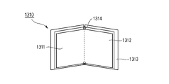
- FIG. 1 is a schematic diagram showing an example of a foldable display device; FIG. It is a mimetic diagram showing an example of a lighting installation concerning one embodiment of the present invention.
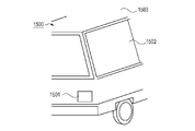
- 1 is a schematic diagram showing an automobile as an example of a moving body according to an embodiment of the present invention;
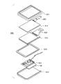
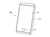
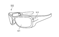
- FIG. 1 is a schematic diagram showing an example of a wearable device according to one embodiment of the present invention;
- FIG. It is an example of the wearable device which concerns on one Embodiment of this invention, and is a schematic diagram which shows the form which has an imaging device.
- Organometallic Complex Represented by Formula (1) As a result of investigations, the present inventors have found an organometallic complex represented by the following general formula (1) in which the decrease in luminous efficiency is reduced even at high current densities.
- M is a metal atom selected from Ir, Pt, Os, Rh, Pd and Ru.
- R 1 to R 8 are each independently selected from hydrogen atoms or substituents. This substituent may be a halogen atom, a cyano group, a nitro group, a trialkylsilyl group, a substituted or unsubstituted alkyl group, a substituted or unsubstituted cycloalkyl group, or a substituted or unsubstituted aryl group having two or less rings. or
- R 9 to R 10 are each independently selected from a hydrogen atom or an alkyl group having 2 or less carbon atoms.
- R 1 to R 8 is the aforementioned substituent, or at least one of R 9 and R 10 is the aforementioned alkyl group having 2 or less carbon atoms.
- M is a metal atom that forms a complex
- specific examples include Ir, Pt, Os, Rh, Pd, Ru, and Re. Among them, Ir is preferable.
- the halogen atoms of R 1 to R 8 are fluorine, chlorine, bromine or iodine atoms. Among them, a fluorine atom is preferable from the viewpoint of thermal stability.
- the alkyl groups in the trialkylsilyl groups of R 1 to R 8 may each independently be an alkyl group having the number of carbon atoms.
- An alkyl group having 1 to 8 carbon atoms is preferable, and may be a straight-chain alkyl group or a branched alkyl group. More specific examples include, but are not limited to, a trimethylsilyl group, a tert-butyldimethylsilyl group, a triisopropylsilyl group, and the like.
- the alkyl groups of R 1 to R 8 may be linear alkyl groups or branched alkyl groups.
- the alkyl group can have from 1 to 20 carbon atoms and can have from 1 to 8 carbon atoms.
- the cycloalkyl groups of R 1 to R 8 and R 11 to R 18 may have 3 to 20 carbon atoms, and may have 3 to 10 carbon atoms. Cyclohexane or cyclopentane are preferred. A carbon atom of the cycloalkyl group may be replaced with an oxygen atom, but it is not preferable to replace two consecutive carbon atoms with oxygen atoms. One carbon atom may be replaced with an oxygen atom.
- bicyclic or less aryl groups include phenyl, naphthyl, pyridyl, benzothienyl, benzofuryl, benzoxazolyl, quinolinyl, and isoquinolinyl groups.
- a phenyl group is preferred.
- aryl groups include phenyl, naphthyl, biphenyl, fluorenyl, phenanthrenyl, anthracenyl, pyridine, carbazolyl, dibenzofuryl, and dibenzothienyl groups.
- the alkyl group or cycloalkyl group may further have a substituent, and examples of the substituent include a halogen atom, a cyano group, and a nitro group.
- the halogen atom that can be substituted on the alkyl group is any one of a fluorine atom, a chlorine atom, a bromine atom and an iodine atom. Among them, a fluorine atom is preferable from the viewpoint of thermal stability.
- the aryl group may have an alkyl group as a substituent.
- the aryl group includes those further having a substituent, specifically, phenyl group, 1-naphthyl group, 2-naphthyl group, 4-biphenyl group, 2-fluorenyl group, 9-phenanthryl group , 2-anthryl group, 1-pyrenyl group, 1-imidazolyl group, 2-furyl group, 3-benzofuryl group, 4-dibenzofuryl group, 2-thienyl group, 3-benzothienyl group, 2-dibenzothienyl group, 2 -pyridyl group, 2-pyrimidinyl group, 1-indolyl group, 2-indolyl group, 9-carbazolyl group, p-chlorophenyl group, o-tolyl group, 4-methoxyphenyl group, 4'-(1-hexynyl)phenyl group , 2-(1-(1,1,2,2,3,3,4,4,5,5,6,6,7,7,8,8
- R9 to R10 are each independently selected from a hydrogen atom and an alkyl group having 2 or less carbon atoms. Specifically, it is a hydrogen atom, a methyl group or an ethyl group.
- the organometallic complex according to the present invention has the effect of reducing the decrease in luminous efficiency at high current densities. That is, it is an organometallic complex with excellent roll-off properties.
- both R 9 and R 10 may be hydrogen atoms.
- Each of R 1 to R 4 may be independently selected from a hydrogen atom or the above alkyl group. It is preferred that R 3 is a tert-butyl group.
- R 5 to R 8 may each be independently selected from a hydrogen atom or the above alkyl group.
- the aryl group can be used without being limited to two rings or less. That is, general formula (1) may be within the following range.
- R 1 , R 2 , R 4 to R 8 are each independently selected from hydrogen atoms or substituents.
- the substituents are halogen atoms, cyano groups, nitro groups, trialkylsilyl groups, substituted or unsubstituted alkyl groups, substituted or unsubstituted cycloalkyl groups, or substituted or unsubstituted phenyl groups.
- R3 is selected from a hydrogen atom , a halogen atom, a cyano group, a nitro group, a trialkylsilyl group, a substituted or unsubstituted alkyl group, a substituted or unsubstituted cycloalkyl group and a substituted or unsubstituted aryl group.
- R 9 to R 10 are each independently selected from a hydrogen atom and an alkyl group having 2 or less carbon atoms. However, R 1 to R 8 are not hydrogen atoms, or at least one of R 9 and R 10 is the alkyl group having 2 or less carbon atoms.
- R 9 and R 10 in the general formula (1) are an alkyl group having 2 or less carbon atoms
- the aryl group in R 1 to R 8 may be used without being limited to bicyclic or less. can be done.
- R 9 or R 10 is an alkyl group having 2 or less carbon atoms
- R 9 is preferably the alkyl group having 2 or less carbon atoms. That is, it may be in the range of general formula (1) or less.
- R 1 to R 8 are each independently selected from hydrogen atoms or substituents.
- the substituents are halogen atoms, cyano groups, nitro groups, trialkylsilyl groups, substituted or unsubstituted alkyl groups, substituted or unsubstituted cycloalkyl groups or substituted or unsubstituted aryl groups.
- R 9 to R 10 are each independently selected from a hydrogen atom and an alkyl group having 2 or less carbon atoms. However, at least one of R 9 and R 10 is the aforementioned alkyl group having 2 or less carbon atoms.
- organometallic complexes of the present invention are exemplified below.
- An iridium complex is given as an example, but the same is true when other metals are used.
- the number of ligands may be appropriately changed depending on the coordination number of the metal.
- the following exemplified compounds have high solvent solubility and can be preferably used for the film formation method by the coating method.
- the organic light-emitting device has at least a first electrode and a second electrode, which are a pair of electrodes, and an organic compound layer arranged between these electrodes.
- the organic compound layer may be a single layer or a multi-layer laminate as long as it has a light-emitting layer.
- a pair of electrodes may be an anode and a cathode.
- the organic compound layer when the organic compound layer is a laminate composed of multiple layers, the organic compound layer may have a light-emitting layer.
- the organic compound layer may have a hole injection layer, a hole transport layer, an electron blocking layer, a hole/exciton blocking layer, an electron transport layer, an electron injection layer, etc., in addition to the light emitting layer.
- the light-emitting layer may be a single layer, or may be a laminate composed of a plurality of layers.
- a hole transport layer and an electron transport layer are also referred to as a charge transport layer.
- the organic light-emitting device of the present embodiment contains the organometallic complex of the present embodiment.
- the organometallic complex according to the present embodiment is applied to any of the above-described hole injection layer, hole transport layer, electron blocking layer, light emitting layer, hole/exciton blocking layer, electron transport layer, electron injection layer, and the like. It is contained, preferably in the light-emitting layer.
- the transport layers between the first electrode and the emissive layer can be referred to as the first charge transport layer.
- the transport layers between the second electrode and the light-emitting layer can be referred to as the second charge transport layer. That is, it can be said that the light emitting layer is in contact with the first charge transport layer and in contact with the second charge transport layer.
- the light-emitting layer when the organic metal complex according to this embodiment is included in the light-emitting layer, the light-emitting layer may be a layer composed only of the organic metal complex according to this embodiment, or It may be a layer containing a first organic compound and a second organic compound different from the first organic compound, in addition to the organometallic complex according to the embodiment.
- the first organic compound may have a lowest excited triplet energy that is greater than the lowest excited triplet energy of the iridium complex of the present invention.
- the lowest excited triplet energy of the second organic compound may be equal to or higher than the lowest excited triplet energy of the organometallic complex of the present invention and equal to or lower than the lowest excited triplet energy of the first organic compound.
- the first organic compound may be a host of the light-emitting layer.
- the second organic compound may be an assist material.
- Organometallic complexes according to the present invention may be guests or dopants.
- the host is a compound that has the largest weight ratio among the compounds that constitute the light-emitting layer.
- the guest or dopant is a compound having a weight ratio smaller than that of the host among the compounds constituting the light-emitting layer, and is responsible for the main light emission.
- the assist material is a compound which has a weight ratio smaller than that of the host among the compounds constituting the light-emitting layer and which assists light emission of the guest. Note that the assist material is also called a second host.
- the concentration of the guest is preferably 0.01% by weight or more and 20% by weight or less with respect to the entire light-emitting layer. It is more preferable that the weight percentage is not less than 10.0% by weight.
- the entire light-emitting layer represents the total weight of the compounds constituting the light-emitting layer.
- the lowest excited triplet energy of the first charge transport layer is preferably higher than the lowest excited triplet energy of the first organic compound.
- the lowest excited triplet energy of the second charge transport layer is preferably higher than the lowest excited triplet energy of the first organic compound.
- the lowest excited triplet energy of the charge transport layer can be estimated from the lowest excited triplet energy of the constituent material of the layer. If the charge transport layer is composed of multiple materials, it may be the lowest excited triplet energy of the compound in greater weight ratio.
- This luminescent layer may be a single layer or multiple layers, and it is possible to mix the luminescent color of this embodiment by including a luminescent material having another luminescent color.
- a multilayer means a state in which a plurality of light-emitting layers are laminated.
- the emission color of the organic light-emitting element is not limited to the same hue as the emission color of the single layer. More specifically, it may be white or a neutral color. In the case of white light, white light may be obtained by emitting red, blue, and green light from each light-emitting layer, or white light may be obtained by combining complementary colors.
- the organometallic complex according to this embodiment can also be used as a constituent material of an organic compound layer other than the light-emitting layer that constitutes the organic light-emitting device of this embodiment. Specifically, it may be used as a constituent material for an electron transport layer, an electron injection layer, a hole transport layer, a hole injection layer, a hole blocking layer, and the like.
- conventionally known low-molecular-weight and high-molecular-weight hole-injecting compounds or hole-transporting compounds, host compounds, light-emitting compounds, and electron-injecting compounds are optionally used.
- a compound or an electron-transporting compound or the like can be used together. Examples of these compounds are given below.
- a material having high hole mobility is preferable so that holes can be easily injected from the anode and the injected holes can be transported to the light-emitting layer.
- a material having a high glass transition temperature is preferred.
- low-molecular-weight and high-molecular-weight materials having hole injection and transport properties include triarylamine derivatives, arylcarbazole derivatives, phenylenediamine derivatives, triazole derivatives, oxadiazole derivatives, imidazole derivatives, stilbene derivatives, phthalocyanine derivatives, porphyrin derivatives, poly Conductive polymers such as arylamine derivatives, polyvinylcarbazole derivatives, polythiophene derivatives, PEDOT-PSS, and copolymers or mixtures thereof may be mentioned. Furthermore, the above hole injection transport materials are also suitably used for the electron blocking layer.
- luminescent materials include condensed ring compounds (such as fluorene derivatives, naphthalene derivatives, pyrene derivatives, perylene derivatives, tetracene derivatives, anthracene derivatives, rubrene, etc.), quinacridone derivatives, coumarin derivatives, stilbene derivatives, tris(8-quinolinolato)aluminum.
- iridium complexes such as tris(2-phenylpyridinate)iridium, platinum complexes, rhenium complexes, copper complexes, europium complexes, ruthenium complexes, and poly(phenylene vinylene) derivatives, poly(fluorene) derivatives, Polymer derivatives such as poly(phenylene) derivatives are included.
- Examples of the light-emitting layer host or light-emitting assist material contained in the light-emitting layer include aromatic hydrocarbon compounds or derivatives thereof, carbazole derivatives, dibenzofuran derivatives, dibenzothiophene derivatives, triazine derivatives, and organic aluminum such as tris(8-quinolinolato)aluminum.
- Polymers such as complexes, organic beryllium complexes, polyphenylene derivatives, polyphenylenevinylene derivatives, polyfluorene derivatives, polyvinylcarbazole derivatives, and copolymers or mixtures thereof can be mentioned.
- the electron-transporting material can be arbitrarily selected from those capable of transporting electrons injected from the cathode to the light-emitting layer, and is selected in consideration of the balance with the hole mobility of the hole-transporting material.
- Materials having electron transport properties include oxadiazole derivatives, oxazole derivatives, pyrazine derivatives, triazole derivatives, triazine derivatives, quinoline derivatives, quinoxaline derivatives, phenanthroline derivatives, organoaluminum complexes, condensed ring compounds (e.g., fluorene derivatives, naphthalene derivatives, chrysene derivatives, anthracene derivatives, etc.). Furthermore, the above electron-transporting materials are also suitably used for the hole blocking layer.
- the electron-injecting material can be arbitrarily selected from those that allow electrons to be easily injected from the cathode, and is selected in consideration of the balance with the hole-injecting property.
- Organic compounds also include n-type dopants and reducing dopants. Examples thereof include compounds containing alkali metals such as lithium fluoride, lithium complexes such as lithium quinolinol, benzimidazolidene derivatives, imidazolidene derivatives, fulvalene derivatives and acridine derivatives.
- An organic light-emitting element is provided by forming a first electrode, an organic compound layer, and a second electrode on an insulating layer provided on a substrate.
- a protective layer, a color filter, etc. may be provided on the second electrode.
- a planarization layer may be provided between it and the protective layer.
- the planarizing layer can be made of acrylic resin or the like. Either the first electrode or the second electrode may be an anode and the other may be a cathode.
- substrates examples include quartz, glass, silicon wafers, resins, and metals.
- a switching element such as a transistor and wiring may be provided on the substrate, and an insulating layer may be provided thereon. Any material can be used for the insulating layer as long as a contact hole can be formed in order to ensure conduction between the anode and the wiring, and insulation from wiring that is not connected can be ensured.
- a resin such as polyimide, silicon oxide, silicon nitride, or the like can be used.
- a pair of electrodes can be used as the electrodes.
- the pair of electrodes may be an anode and a cathode.
- the electrode with the higher potential is the anode, and the other is the cathode.
- the electrode that supplies holes to the light-emitting layer is the anode, and the electrode that supplies electrons is the cathode.
- a material with a work function that is as large as possible is good for the constituent material of the anode.
- simple metals such as gold, platinum, silver, copper, nickel, palladium, cobalt, selenium, vanadium, tungsten, mixtures containing these, or alloys combining these, tin oxide, zinc oxide, indium oxide, indium oxide Metal oxides such as tin (ITO) and indium zinc oxide can be used.
- Conductive polymers such as polyaniline, polypyrrole and polythiophene can also be used.
- the anode may be composed of a single layer, or may be composed of a plurality of layers.
- chromium, aluminum, silver, titanium, tungsten, molybdenum, or alloys or laminates thereof can be used.
- a transparent conductive layer of oxide such as indium tin oxide (ITO) or indium zinc oxide can be used, but the material is not limited to these.
- ITO indium tin oxide
- a photolithography technique can be used to form the electrodes.
- a material with a small work function is preferable as a constituent material of the cathode.
- alkali metals such as lithium, alkaline earth metals such as calcium, simple metals such as aluminum, titanium, manganese, silver, lead, and chromium, or mixtures thereof may be used.
- alloys obtained by combining these simple metals can also be used.
- magnesium-silver, aluminum-lithium, aluminum-magnesium, silver-copper, zinc-silver and the like can be used.
- Metal oxides such as indium tin oxide (ITO) can also be used. These electrode materials may be used singly or in combination of two or more.
- the cathode may be of a single-layer structure or a multi-layer structure.
- it is preferable to use silver and in order to suppress aggregation of silver, a silver alloy is more preferable. As long as aggregation of silver can be suppressed, the ratio of the alloy does not matter. For example, it may be 1:1.
- the cathode may be a top emission device using an oxide conductive layer such as indium tin oxide (ITO), or may be a bottom emission device using a reflective electrode such as aluminum (Al), and is not particularly limited. .
- the method for forming the cathode is not particularly limited, but it is more preferable to use a direct current or alternating current sputtering method or the like because the film coverage is good and the resistance can be easily lowered.
- a protective layer may be provided over the cathode. For example, by adhering glass provided with a moisture absorbent on the cathode, it is possible to reduce the penetration of water or the like into the organic compound layer and reduce the occurrence of display defects.
- a passivation film such as silicon nitride may be provided on the cathode to reduce penetration of water or the like into the organic compound layer.
- a silicon nitride film having a thickness of 2 ⁇ m may be formed by a CVD method as a protective layer.
- a protective layer may be provided using an atomic deposition method (ALD method) after film formation by the CVD method.
- a color filter may be provided on the protective layer.
- a color filter considering the size of the organic light-emitting element may be provided on another substrate and then bonded to the substrate provided with the organic light-emitting element.
- a color filter may be patterned.
- the color filters may be composed of polymers.
- a planarization layer may be provided between the color filter and the protective layer.
- the planarization layer may be composed of an organic compound, and may be a low-molecular or high-molecular compound, preferably a high-molecular compound.
- the planarization layer may be provided above and below the color filter, and the constituent materials thereof may be the same or different.
- Specific examples include polyvinylcarbazole resin, polycarbonate resin, polyester resin, ABS resin, acrylic resin, polyimide resin, phenol resin, epoxy resin, silicon resin, urea resin, and the like.
- a counter substrate may be provided over the planarization layer.
- the counter substrate is called the counter substrate because it is provided at a position corresponding to the substrate described above.
- the constituent material of the counter substrate may be the same as that of the aforementioned substrate.
- the opposing substrate may be the second substrate when the substrate described above is the first substrate.
- organic compound layers (hole injection layer, hole transport layer, electron blocking layer, light emitting layer, hole blocking layer, electron transport layer, electron injection layer, etc.) constituting the organic light emitting device according to one embodiment of the present invention are described below. It is formed by the method shown.
- the organic compound layer constituting the organic light-emitting device is not particularly limited, a dry process or a wet process can be used.
- dry processes that can be used include dry processes such as vacuum deposition, ionization deposition, sputtering, and plasma.
- wet processes include known coating methods (e.g., spin coating method, casting method, micro gravure coating method, gravure coating method, bar coating method, roll coating method, wire bar coating method, dip coating method, spray coating method, screen printing method, flexographic printing method, offset printing method, inkjet printing method, capillary coating method, nozzle coating method, etc.) can be used.
- the vacuum vapor deposition method, the ionization vapor deposition method, the inkjet printing method, the nozzle coating method, and the like are suitable for manufacturing large-area organic light-emitting devices.
- each layer in the organic light-emitting device is preferably from 1 nm to 10 ⁇ m.
- the film thickness of the light-emitting layer of the organic compound layer is preferably 10 nm to 100 nm in order to obtain effective light-emitting properties.
- the composition of these layers is dissolved in a solvent to form an ink.
- the viscosity of this ink may be adjusted according to the type of printing method.
- an ink is applied to a printing method such as an inkjet printing method in which a solution passes through an ejection device, it is preferably 1 to 20 mPa ⁇ s at 25° C. in order to reduce clogging and flight deflection during ejection. is.
- a solvent having a boiling point of 70°C to 300°C under 1 atmospheric pressure can be used as the ink.
- the amount of the organic solvent is usually 10 to 100 parts by mass with respect to 1 part by mass of the material forming each organic compound layer.
- the drying of the coating film obtained by the wet process can be appropriately selected according to the type of each layer. Usually, it can be heated at 100 to 250° C., preferably 110 to 200° C., for 5 to 60 minutes in an air atmosphere or an inert gas (nitrogen, argon, etc.) atmosphere. Further, heating may be performed under normal pressure (1 atm) or reduced pressure (100 Pa to 0.1 MPa). The temperature, pressure and time in this drying process can be adjusted to remove the solvent in each layer.
- binder resin examples include polyvinylcarbazole resins, polycarbonate resins, polyester resins, ABS resins, acrylic resins, polyimide resins, phenol resins, epoxy resins, silicone resins, and urea resins, but are not limited to these. .
- binder resins may be used singly as homopolymers or copolymers, or two or more may be used in combination.
- additives such as known plasticizers, antioxidants, and ultraviolet absorbers may be used in combination.
- a light emitting device may have a pixel circuit connected to a light emitting element.
- the pixel circuit may be of an active matrix type that independently controls light emission of the first light emitting element and the second light emitting element. Active matrix circuits may be voltage programmed or current programmed.
- the drive circuit has a pixel circuit for each pixel.
- the pixel circuit includes a light emitting element, a transistor that controls the light emission luminance of the light emitting element, a transistor that controls the light emission timing, a capacitor that holds the gate voltage of the transistor that controls the light emission luminance, and a capacitor for connecting to GND without passing through the light emitting element. It may have a transistor.
- a light-emitting device has a display area and a peripheral area arranged around the display area.
- the display area has a pixel circuit
- the peripheral area has a display control circuit.
- the mobility of the transistors forming the pixel circuit may be lower than the mobility of the transistors forming the display control circuit.
- the gradient of the current-voltage characteristics of the transistors that make up the pixel circuit may be smaller than the gradient of the current-voltage characteristics of the transistors that make up the display control circuit.
- the slope of the current-voltage characteristic can be measured by the so-called Vg-Ig characteristic.
- a transistor that constitutes a pixel circuit is a transistor that is connected to a light emitting element such as a first light emitting element.
- An organic light emitting device has a plurality of pixels.
- a pixel has sub-pixels that emit different colors from each other.
- the sub-pixels may each have, for example, RGB emission colors.
- a pixel emits light in a region called a pixel aperture. This area is the same as the first area.
- the pixel aperture may be 15 ⁇ m or less and may be 5 ⁇ m or more. More specifically, it may be 11 ⁇ m, 9.5 ⁇ m, 7.4 ⁇ m, 6.4 ⁇ m, or the like.
- the distance between sub-pixels may be 10 ⁇ m or less, specifically 8 ⁇ m, 7.4 ⁇ m, and 6.4 ⁇ m.
- the pixels can take a known arrangement form in a plan view. Examples may be a stripe arrangement, a delta arrangement, a pentile arrangement, a Bayer arrangement.
- the shape of the sub-pixel in plan view may take any known shape. For example, a rectangle, a square such as a rhombus, a hexagon, and the like. Of course, if it is not an exact figure but has a shape close to a rectangle, it is included in the rectangle.
- a combination of sub-pixel shapes and pixel arrays can be used.
- An organic light-emitting device can be used as a constituent member of a display device or a lighting device.
- Other applications include exposure light sources for electrophotographic image forming apparatuses, backlights for liquid crystal display devices, and light emitting devices having color filters as white light sources.
- the display device has an image input unit for inputting image information from an area CCD, a linear CCD, a memory card, etc., has an information processing unit for processing the input information, and displays the input image on the display unit. It may be an image information processing apparatus that
- the display unit of the imaging device or inkjet printer may have a touch panel function.
- the driving method of this touch panel function may be an infrared method, a capacitive method, a resistive film method, or an electromagnetic induction method, and is not particularly limited.
- the display device may also be used as a display section of a multi-function printer.
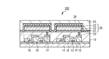
- FIG. 1A is a cross-sectional schematic diagram of an example of a pixel that constitutes a display device according to this embodiment.
- the pixel has sub-pixels 10 .
- the sub-pixels are divided into 10R, 10G, and 10B according to their light emission.
- the emission color may be distinguished by the wavelength of light emitted from the light-emitting layer, or the light emitted from the sub-pixel may be selectively transmitted or color-converted by a color filter or the like.
- Each sub-pixel has a reflective electrode 2 as a first electrode on an interlayer insulating layer 1, an insulating layer 3 covering the edge of the reflective electrode 2, an organic compound layer 4 covering the first electrode and the insulating layer, and a transparent electrode 5. , a protective layer 6 and a color filter 7 .
- the interlayer insulating layer 1 may have transistors and capacitive elements arranged under or inside it.
- the transistor and the first electrode may be electrically connected through a contact hole (not shown) or the like.
- the insulating layer 3 is also called a bank or a pixel separation film. It covers the edge of the first electrode and surrounds the first electrode. A portion where the insulating layer is not arranged is in contact with the organic compound layer 4 and becomes a light emitting region.
- the organic compound layer 4 has a hole injection layer 41 , a hole transport layer 42 , a first light emitting layer 43 , a second light emitting layer 44 and an electron transport layer 45 .
- the second electrode 5 may be a transparent electrode, a reflective electrode, or a transflective electrode.
- the protective layer 6 reduces penetration of moisture into the organic compound layer. Although the protective layer is shown as one layer, it may be multiple layers. Each layer may have an inorganic compound layer and an organic compound layer.
- the color filter 7 is divided into 7R, 7G, and 7B according to its color.
- the color filters may be formed on a planarizing film (not shown). Also, a resin protective layer (not shown) may be provided on the color filter. Also, a color filter may be formed on the protective layer 6 . Alternatively, after being provided on a counter substrate such as a glass substrate, they may be attached together.
- FIG. 1B is a schematic cross-sectional view showing an example of a display device having an organic light emitting element and a transistor connected to the organic light emitting element.
- a transistor is an example of an active device.
- the transistors may be thin film transistors (TFTs).
- a display device 100 in FIG. 1B includes a substrate 11 made of glass, silicon, or the like, and an insulating layer 12 provided thereon.
- An active element 18 such as a TFT is arranged on the insulating layer, and a gate electrode 13, a gate insulating film 14, and a semiconductor layer 15 of the active element are arranged.
- the TFT 18 is also composed of a semiconductor layer 15 , a drain electrode 16 and a source electrode 17 .
- An insulating film 19 is provided on the TFT 18 .
- An anode 21 and a source electrode 17 constituting the organic light-emitting element are connected through a contact hole 20 provided in the insulating film.
- the method of electrical connection between the electrodes (anode, cathode) included in the organic light-emitting element and the electrodes (source electrode, drain electrode) included in the TFT is not limited to the mode shown in FIG. 1B. That is, it is sufficient that either one of the anode or the cathode is electrically connected to one of the TFT source electrode and the TFT drain electrode.
- TFT refers to a thin film transistor.
- the organic compound layer is illustrated as one layer, but the organic compound layer 22 may be multiple layers.
- a first protective layer 24 and a second protective layer 25 are provided on the cathode 23 to reduce deterioration of the organic light-emitting element.
- transistors are used as switching elements in the display device 100 of FIG. 1B, other switching elements may be used instead.
- the transistors used in the display device 100 of FIG. 2(b) are not limited to transistors using a single crystal silicon wafer, and may be thin film transistors having an active layer on the insulating surface of the substrate.
- active layers include non-single-crystal silicon such as single-crystal silicon, amorphous silicon, and microcrystalline silicon, and non-single-crystal oxide semiconductors such as indium zinc oxide and indium gallium zinc oxide.
- a thin film transistor is also called a TFT element.
- a transistor included in the display device 100 of FIG. 1B may be formed in a substrate such as a Si substrate.
- a substrate such as a Si substrate.
- formed in a substrate means that a substrate itself such as a Si substrate is processed to fabricate a transistor.
- having a transistor in a substrate can be regarded as forming the substrate and the transistor integrally.
- the organic light-emitting element according to the present embodiment is controlled in emission luminance by a TFT, which is an example of a switching element, and by providing the organic light-emitting elements in a plurality of planes, an image can be displayed with each emission luminance.
- the switching elements according to the present embodiment are not limited to TFTs, and may be transistors made of low-temperature polysilicon, or active matrix drivers formed on a substrate such as a Si substrate. On the substrate can also mean inside the substrate. Whether the transistor is provided in the substrate or the TFT is used is selected depending on the size of the display portion. For example, if the size is about 0.5 inch, it is preferable to provide the organic light emitting element on the Si substrate.
- FIG. 2 is a schematic diagram showing an example of the display device according to this embodiment.
- Display device 1000 may have touch panel 1003 , display panel 1005 , frame 1006 , circuit board 1007 , and battery 1008 between upper cover 1001 and lower cover 1009 .
- the touch panel 1003 and the display panel 1005 are connected to flexible printed circuits FPCs 1002 and 1004 .
- Transistors are printed on the circuit board 1007 .
- the battery 1008 may not be provided if the display device is not a portable device, or may be provided at another position even if the display device is a portable device.
- the display device may have color filters having red, green, and blue.
- the color filters may be arranged in a delta arrangement of the red, green, and blue colors, in a stripe arrangement, or in a mosaic arrangement.
- the display device may be used in the display section of a mobile terminal. In that case, it may have both a display function and an operation function.
- Mobile terminals include mobile phones such as smart phones, tablets, head-mounted displays, and the like.
- the display device may be used in the display section of an imaging device having an optical section having a plurality of lenses and an imaging device that receives light that has passed through the optical section.
- the imaging device may have a display unit that displays information acquired by the imaging element.
- the display section may be a display section exposed to the outside of the imaging device, or may be a display section arranged within the viewfinder.
- the imaging device may be a digital camera or a digital video camera. An imaging device can also be called a photoelectric conversion device.
- FIG. 3A is a schematic diagram showing an example of an imaging device according to this embodiment.
- the imaging device 1100 may have a viewfinder 1101 , a rear display 1102 , an operation unit 1103 and a housing 1104 .
- the viewfinder 1101 may have a display device according to this embodiment.
- the display device may display not only the image to be captured, but also environmental information, imaging instructions, and the like.
- the environmental information may include the intensity of outside light, the direction of outside light, the moving speed of the subject, the possibility of the subject being blocked by an obstacle, and the like.
- a display device using the organic light-emitting device of the present invention Since the best time to take an image is a short amount of time, it is better to display the information as soon as possible. Therefore, it is preferable to use a display device using the organic light-emitting device of the present invention. This is because the organic light emitting device has a high response speed.
- a display device using an organic light-emitting element can be used more preferably than these devices and a liquid crystal display device, which require a high display speed.
- the imaging device 1100 has an optical unit (not shown).
- the optical unit has a plurality of lenses and forms an image on the imaging device housed in the housing 1104 .
- the multiple lenses can be focused by adjusting their relative positions. This operation can also be performed automatically.
- FIG. 3B is a schematic diagram showing an example of the electronic device according to this embodiment.
- Electronic device 1200 includes display portion 1201 , operation portion 1202 , and housing 1203 .
- the housing 1203 may include a circuit, a printed board including the circuit, a battery, and a communication portion.
- the operation unit 1202 may be a button or a touch panel type reaction unit.
- the operation unit may be a biometric recognition unit that recognizes a fingerprint and performs unlocking or the like.
- An electronic device having a communication unit can also be called a communication device.
- the electronic device may further have a camera function by being provided with a lens and an imaging device. An image captured by the camera function is displayed on the display unit. Examples of electronic devices include smartphones, notebook computers, and the like.
- FIG. 4A and 4B are schematic diagrams showing an example of the display device according to this embodiment.
- FIG. 4A shows a display device such as a television monitor or a PC monitor.
- a display device 1300 has a frame 1301 and a display portion 1302 .
- the light emitting device according to this embodiment may be used for the display unit 1302 .
- the base 1303 is not limited to the form of FIG. 4A.
- the lower side of the frame 1301 may also serve as the base.
- the frame 1301 and the display unit 1302 may be curved. Its radius of curvature may be between 5000 mm and 6000 mm.
- FIG. 4B is a schematic diagram showing another example of the display device according to this embodiment.
- a display device 1310 in FIG. 4B is configured to be foldable, and is a so-called foldable display device.
- the display device 1310 has a first display portion 1311 , a second display portion 1312 , a housing 1313 and a bending point 1314 .
- the first display unit 1311 and the second display unit 1312 may have the light emitting device according to this embodiment.
- the first display portion 1311 and the second display portion 1312 may be a seamless display device.
- the first display portion 1311 and the second display portion 1312 can be separated at a bending point.
- the first display unit 1311 and the second display unit 1312 may display different images, or the first and second display units may display one image.
- FIG. 5A is a schematic diagram showing an example of the lighting device according to this embodiment.
- the illumination device 1400 may have a housing 1401 , a light source 1402 , a circuit board 1403 , an optical film 1404 and a light diffusion section 1405 .
- the light source may comprise an organic light emitting device according to this embodiment.
- the optical filter may be a filter that enhances the color rendering of the light source.
- the light diffusing portion can effectively diffuse the light from the light source such as lighting up and deliver the light over a wide range.
- the optical filter and the light diffusion section may be provided on the light exit side of the illumination. If necessary, a cover may be provided on the outermost part.
- a lighting device is, for example, a device that illuminates a room.
- the lighting device may emit white, neutral white, or any other color from blue to red. It may have a dimming circuit to dim them.
- the lighting device may have the organic light emitting device of the present invention and a power supply circuit connected thereto.
- a power supply circuit is a circuit that converts an AC voltage into a DC voltage. Further, white has a color temperature of 4200K, and neutral white has a color temperature of 5000K.
- the lighting device may have color filters.
- the lighting device according to the present embodiment may have a heat dissipation section.
- the heat radiating part is for radiating the heat inside the device to the outside of the device, and may be made of metal, liquid silicon, or the like, which has a high specific heat.
- FIG. 5B is a schematic diagram of an automobile, which is an example of a moving body according to this embodiment.
- the automobile has a tail lamp, which is an example of a lamp.
- the automobile 1500 may have a tail lamp 1501, and may be configured to turn on the tail lamp when a brake operation or the like is performed.
- the tail lamp 1501 may have the organic light emitting device according to this embodiment.
- the tail lamp may have a protective member that protects the organic light emitting elements.
- the protective member may be made of any material as long as it has a certain degree of strength and is transparent, but is preferably made of polycarbonate or the like. A furandicarboxylic acid derivative, an acrylonitrile derivative, or the like may be mixed with the polycarbonate.
- a car 1500 may have a body 1503 and a window 1502 attached thereto.
- the window may be a transparent display unless it is a window for checking the front and rear of the automobile.
- the transparent display may comprise an organic light emitting device according to the present embodiments. In this case, constituent materials such as electrodes of the organic light-emitting element are made of transparent members.
- a mobile object may be a ship, an aircraft, a drone, or the like.
- the moving body may have a body and a lamp provided on the body.
- the lighting device may emit light to indicate the position of the aircraft.
- the lamp has the organic light-emitting element according to this embodiment.
- the display device can be applied to systems that can be worn as wearable devices such as smart glasses, HMDs, and smart contacts.
- An imaging display device used in such an application includes an imaging device capable of photoelectrically converting visible light and a display device capable of emitting visible light.
- FIG. 6A illustrates glasses 1600 (smart glasses) according to one application example.
- An imaging device 1602 such as a CMOS sensor or SPAD is provided on the surface side of lenses 1601 of spectacles 1600 . Further, the display device of each embodiment described above is provided on the rear surface side of the lens 1601 .
- the spectacles 1600 further include a control device 1603 .
- the control device 1603 functions as a power supply that supplies power to the imaging device 1602 and the display device according to each embodiment. Also, the control device 1603 controls operations of the imaging device 1602 and the display device.
- the lens 1601 is formed with an optical system for condensing light onto the imaging device 1602 .
- FIG. 6B illustrates glasses 1610 (smart glasses) according to one application.
- the glasses 1610 have a control device 1612, and the control device 1612 is equipped with an imaging device corresponding to the imaging device 1602 and a display device.
- An imaging device in the control device 1612 and an optical system for projecting light emitted from the display device are formed in the lens 1611 , and an image is projected onto the lens 1611 .
- the control device 1612 functions as a power source that supplies power to the imaging device and the display device, and controls the operation of the imaging device and the display device.
- the control device may have a line-of-sight detection unit that detects the line of sight of the wearer. Infrared rays may be used for line-of-sight detection.
- the infrared light emitting section emits infrared light to the eyeballs of the user who is gazing at the displayed image.
- a captured image of the eyeball is obtained by detecting reflected light of the emitted infrared light from the eyeball by an imaging unit having a light receiving element.
- the user's line of sight to the displayed image is detected from the captured image of the eyeball obtained by capturing infrared light.
- Any known method can be applied to line-of-sight detection using captured images of eyeballs.
- line-of-sight detection processing is performed based on the pupillary corneal reflection method.
- the user's line of sight is detected by calculating a line of sight vector representing the orientation (rotational angle) of the eyeball based on the pupil image and the Purkinje image included in the captured image of the eyeball using the pupillary corneal reflection method. be.
- a display device may have an imaging device having a light-receiving element, and may control a display image of the display device based on user's line-of-sight information from the imaging device.
- the display device determines, based on the line-of-sight information, a first visual field area that the user gazes at, and a second visual field area other than the first visual field area.
- the first viewing area and the second viewing area may be determined by the control device of the display device, or may be determined by an external control device.
- the display resolution of the first viewing area may be controlled to be higher than the display resolution of the second viewing area. That is, the resolution of the second viewing area may be lower than that of the first viewing area.
- the display area has a first display area and a second display area different from the first display area. is determined the region where is high.
- the first viewing area and the second viewing area may be determined by the control device of the display device, or may be determined by an external control device.
- the resolution of areas with high priority may be controlled to be higher than the resolution of areas other than areas with high priority. That is, the resolution of areas with relatively low priority may be lowered.
- AI may be used to determine the first field of view area and areas with high priority.
- the AI is a model configured to estimate the angle of the line of sight from the eyeball image and the distance to the object ahead of the line of sight, using the image of the eyeball and the direction in which the eyeball of the image was actually viewed as training data. It can be.
- the AI program may be possessed by the display device, the imaging device, or the external device. If the external device has it, it is communicated to the display device via communication.
- display control When display control is performed based on visual recognition detection, it can be preferably applied to smart glasses that further have an imaging device that captures an image of the outside. Smart glasses can display captured external information in real time.
- the device using the organic light-emitting element according to the present embodiment it is possible to achieve both good outdoor visibility and power-saving display through highly efficient and high-brightness light output.
- Example 1 Compound (4) obtained in Synthesis Example 1 was purified by sublimation at 360° C. and 3 ⁇ 10 ⁇ 3 Pa. The HPLC purity of the sublimate was 99.9%.
- an organic light emitting device having a structure of anode/hole injection layer/hole transport layer/electron blocking layer/light emitting layer/hole blocking layer/electron transport layer/cathode was fabricated on a substrate in the following manner. bottom.
- ITO substrate A 100 nm-thick film of ITO as an anode was formed on a glass substrate by a sputtering method and used as a transparent conductive support substrate (ITO substrate).
- ITO substrate On this ITO substrate, the following organic compound layers and electrode layers were continuously formed in a vacuum chamber at 1 ⁇ 10 ⁇ 5 Pa by vacuum deposition using resistance heating. At this time, the opposing electrode area was made to be 3 mm 2 .
- Electron transport layer (30 nm) ET20 Metal electrode layer 1 (15 nm) LiF Metal electrode layer 2 (100 nm) Al
- the current efficiency of the obtained organic light-emitting device was measured using the ITO electrode as an anode and the Al electrode as a cathode.
- the current efficiency at a current density of 5 mA/cm 2 was 94.8 cd/A.
- the current efficiency at a current density of 50 mA/cm 2 was 79.2 cd/A.
- Example 2 Compound (13) obtained in Synthesis Example 2 was purified by sublimation in the same manner as Compound (4) of Example 1 to obtain a sublimate with HPLC purity of 99.8%.
- An organic light-emitting device was obtained in the same manner as in Example 1, except that the sublimate of Example 2 was used instead of the sublimate of Example 1.
- the current efficiency of the obtained organic light-emitting device was measured using the ITO electrode as an anode and the Al electrode as a cathode.
- the current efficiency at a current density of 5 mA/cm 2 was 95.0 cd/A.
- the current efficiency at a current density of 50 mA/cm 2 was 80.5 cd/A.
- Example 3 Compound (56) obtained in Synthesis Example 3 was purified by sublimation in the same manner as Compound (4) of Example 1 to obtain a sublimate with HPLC purity of 99.9%.
- An organic light-emitting device was obtained in the same manner as in Example 1, except that the sublimate of Example 3 was used instead of the sublimate of Example 1.
- the current efficiency of the obtained organic light-emitting device was measured using the ITO electrode as an anode and the Al electrode as a cathode.
- the current efficiency at a current density of 5 mA/cm 2 was 91.1 cd/A.
- the current efficiency at a current density of 50 mA/cm 2 was 77.9 cd/A.
- Example 4 Compound (58) obtained in Synthesis Example 4 was purified by sublimation in the same manner as Compound (4) of Example 1 to obtain a sublimate with HPLC purity of 99.9%.
- An organic light-emitting device was obtained in the same manner as in Example 1, except that the sublimate of Example 4 was used instead of the sublimate of Example 1.
- the current efficiency of the obtained organic light-emitting device was measured using the ITO electrode as an anode and the Al electrode as a cathode.
- the current efficiency at a current density of 5 mA/cm 2 was 92.5 cd/A.
- the current efficiency at a current density of 50 mA/cm 2 was 75.5 cd/A.
- Example 5 Compound (70) obtained in Synthesis Example 5 was purified by sublimation in the same manner as Compound (4) of Example 1 to obtain a sublimate with HPLC purity of 99.9%.
- An organic light-emitting device was obtained in the same manner as in Example 1, except that the sublimate of Example 5 was used instead of the sublimate of Example 1.
- the current efficiency of the obtained organic light-emitting device was measured using the ITO electrode as an anode and the Al electrode as a cathode.
- the current efficiency at a current density of 5 mA/cm 2 was 93.0 cd/A.
- the current efficiency at a current density of 50 mA/cm 2 was 78.1 cd/A.
- the current efficiency of the obtained organic light-emitting device was measured using the ITO electrode as an anode and the Al electrode as a cathode.
- the current efficiency at a current density of 5 mA/cm 2 was 75.0 cd/A.
- the current efficiency at a current density of 50 mA/cm 2 was 62.3 cd/A.
- Comparative Example 1 Comparative compound (1) was purified by sublimation in the same manner as compound (4) of Example 1 to obtain a sublimate with an HPLC purity of 99.9%. An organic light-emitting device was obtained in the same manner as in Example 1, except that the sublimate of Comparative Example 1 was used instead of the sublimate of Example 1.
- the current efficiency of the obtained organic light-emitting device was measured using the ITO electrode as an anode and the Al electrode as a cathode.
- the current efficiency at a current density of 5 mA/cm 2 was 85.1 cd/A.
- the current efficiency at a current density of 50 mA/cm 2 was 65.8 cd/A.
- Comparative Example 2 Comparative compound (2) was purified by sublimation in the same manner as compound (4) of Example 1 to obtain a sublimate with an HPLC purity of 99.9%. An organic light-emitting device was obtained in the same manner as in Example 1, except that the sublimate of Comparative Example 3 was used instead of the sublimate of Example 1.
- the current efficiency of the obtained organic light-emitting device was measured using the ITO electrode as an anode and the Al electrode as a cathode.
- the current efficiency at a current density of 5 mA/cm 2 was 86.9 cd/A.
- the current efficiency at a current density of 50 mA/cm 2 was 65.0 cd/A.
- Comparative Example 3 Comparative compound (3) was purified by sublimation in the same manner as compound (4) of Example 1 to obtain a sublimate with HPLC purity of 99.9%. An organic light-emitting device was obtained in the same manner as in Example 1, except that the sublimate of Comparative Example 4 was used instead of the sublimate of Example 1.
- the current efficiency of the obtained organic light-emitting device was measured using the ITO electrode as an anode and the Al electrode as a cathode.
- the current efficiency at a current density of 5 mA/cm 2 was 79.3 cd/A.
- the current efficiency at a current density of 50 mA/cm 2 was 62.0 cd/A.
- Comparative Example 4 Comparative compound (4) was purified by sublimation in the same manner as compound (4) of Example 1 to obtain a sublimate with HPLC purity of 99.8%. An organic light-emitting device was obtained in the same manner as in Example 1, except that the sublimate of Comparative Example 4 was used instead of the sublimate of Example 1.
- the current efficiency of the obtained organic light-emitting device was measured using the ITO electrode as an anode and the Al electrode as a cathode.
- the current efficiency at a current density of 5 mA/cm 2 was 84.8 cd/A.
- the current efficiency at a current density of 50 mA/cm 2 was 66.5 cd/A.
- Comparative Example 5 Comparative compound (5) was purified by sublimation in the same manner as compound (4) of Example 1 to obtain a sublimate with HPLC purity of 99.6%. An organic light-emitting device was obtained in the same manner as in Example 1, except that the sublimate of Comparative Example 5 was used instead of the sublimate of Example 1.
- the current efficiency of the obtained organic light-emitting device was measured using the ITO electrode as an anode and the Al electrode as a cathode.
- the current efficiency at a current density of 5 mA/cm 2 was 86.1 cd/A.
- the current efficiency at a current density of 50 mA/cm 2 was 67.7 cd/A.
- Comparative Example 6 Comparative compound (6) was purified by sublimation in the same manner as compound (4) of Example 1 to obtain a sublimate with HPLC purity of 99.6%. An organic light-emitting device was obtained in the same manner as in Example 1, except that the sublimate of Comparative Example 6 was used instead of the sublimate of Example 1.
- the current efficiency of the obtained organic light-emitting device was measured using the ITO electrode as an anode and the Al electrode as a cathode.
- the current efficiency at a current density of 5 mA/cm 2 was 85.5 cd/A.
- the current efficiency at a current density of 50 mA/cm 2 was 64.0 cd/A.
- Example 6 Using the compound (4) described in Example 1, an organic light-emitting device having a structure of anode/hole injection layer/light-emitting layer/electron transport layer/cathode was produced on a substrate in the following manner.
- ITO substrate A 100 nm-thick film of ITO as an anode was formed on a glass substrate by a sputtering method and used as a transparent conductive support substrate (ITO substrate).
- This ITO substrate was washed with pure water and then with IPA, and after UV-ozone treatment, a hole injection layer was formed by spin coating.
- the film forming conditions are as follows.
- Coating liquid Poly(3,4-ethylenedioxythiophene)polystyrenesulfonic acid aqueous solution (PEDOT; PSS aqueous solution, manufactured by Aldrich, conductivity 1 ⁇ 10 ⁇ 5 S/cm, compound concentration 2.8% by mass)
- PEDOT Poly(3,4-ethylenedioxythiophene)polystyrenesulfonic acid aqueous solution
- Spin coating conditions 3000 rpm, 60 seconds, under nitrogen atmosphere Annealing conditions: 200° C., 1 hour, under nitrogen atmosphere
- Film thickness 40 nm
- a light-emitting layer was formed by spin coating.
- the composition of the coating liquid for forming the light-emitting layer and the film-forming conditions are as follows. Coating liquid: compound (4) 6.0% by mass EM37 94.0% by mass Chlorobenzene 9900% by mass Spin coating conditions: 3000 rpm, 60 seconds, under nitrogen atmosphere Annealing conditions: 110° C., 10 minutes, under nitrogen atmosphere Film thickness: 30 nm
- Electrotransport layer (50 nm) TPBi Metal electrode layer 1: (0.5 nm) LiF Metal electrode layer 2: (90 nm) Al
- the current efficiency of the obtained organic light-emitting device was measured using the ITO electrode as an anode and the Al electrode as a cathode.
- the current efficiency at a current density of 5 mA/cm 2 was 55.9 cd/A.
- the current efficiency at a current density of 50 mA/cm 2 was 45.4 cd/A.
- Example 7 An organic light-emitting device was obtained in the same manner as in Example 6, except that compound (97) having an HPLC purity of 99.8% was used instead of compound (4) of Example 6.
- the current efficiency of the obtained organic light-emitting device was measured using the ITO electrode as an anode and the Al electrode as a cathode.
- the current efficiency at a current density of 5 mA/cm 2 was 53.5 cd/A.
- the current efficiency at a current density of 50 mA/cm 2 was 44.2 cd/A.
- the current efficiency of the obtained organic light-emitting device was measured using the ITO electrode as an anode and the Al electrode as a cathode.
- the current efficiency at a current density of 5 mA/cm 2 was 35.2 cd/A.
- the current efficiency at a current density of 50 mA/cm 2 was 29.1 cd/A.
- the current efficiency of the obtained organic light-emitting device was measured using the ITO electrode as an anode and the Al electrode as a cathode.
- the current efficiency at a current density of 5 mA/cm 2 was 53.0 cd/A.
- the current efficiency at a current density of 50 mA/cm 2 was 40.5 cd/A.
- the current efficiency of the obtained organic light-emitting device was measured using the ITO electrode as an anode and the Al electrode as a cathode.
- the current efficiency at a current density of 5 mA/cm 2 was 56.8 cd/A.
- the current efficiency at a current density of 50 mA/cm 2 was 42.3 cd/A.
- the organometallic complex according to the present invention has a low rate of decrease in luminous efficiency at the second current density, which is higher than the first current density, with respect to the luminous efficiency at the first current density. It is an organometallic complex with excellent off properties.
Landscapes
- Chemical & Material Sciences (AREA)
- Organic Chemistry (AREA)
- Engineering & Computer Science (AREA)
- Physics & Mathematics (AREA)
- Optics & Photonics (AREA)
- Inorganic Chemistry (AREA)
- Materials Engineering (AREA)
- Microelectronics & Electronic Packaging (AREA)
- Crystallography & Structural Chemistry (AREA)
- Geometry (AREA)
- Life Sciences & Earth Sciences (AREA)
- Sustainable Development (AREA)
- Electroluminescent Light Sources (AREA)
Abstract
Description


本発明者らは、検討の結果、高い電流密度においても発光子効率の低下が低減された下記一般式(1)で表される有機金属錯体を見出した。 [Organometallic Complex Represented by Formula (1)]
As a result of investigations, the present inventors have found an organometallic complex represented by the following general formula (1) in which the decrease in luminous efficiency is reduced even at high current densities.


次に、本発明の一実施形態に係る有機発光素子が有する有機化合物層について説明する。本実施形態に係る有機発光素子は、一対の電極である第一電極と第二電極と、これら電極間に配置される有機化合物層と、を少なくとも有する。本実施形態の有機発光素子において、有機化合物層は発光層を有していれば単層であってもよいし複数層からなる積層体であってもよい。一対の電極は陽極と陰極であってよい。 [Organic compound layer of organic light emitting device according to one embodiment of the present invention]
Next, the organic compound layer included in the organic light emitting device according to one embodiment of the present invention will be described. The organic light-emitting device according to this embodiment has at least a first electrode and a second electrode, which are a pair of electrodes, and an organic compound layer arranged between these electrodes. In the organic light-emitting device of the present embodiment, the organic compound layer may be a single layer or a multi-layer laminate as long as it has a light-emitting layer. A pair of electrodes may be an anode and a cathode.


有機発光素子は、基板の上に設けられた絶縁層上に、第一電極、有機化合物層、第二電極を形成して設けられる。第二電極の上には、保護層、カラーフィルタ等を設けてよい。カラーフィルタを設ける場合は、保護層との間に平坦化層を設けてよい。平坦化層はアクリル樹脂等で構成することができる。第一電極、第二電極はいずれかが陽極で、他方が陰極であってよい。 [Structure of Organic Light-Emitting Device]
An organic light-emitting element is provided by forming a first electrode, an organic compound layer, and a second electrode on an insulating layer provided on a substrate. A protective layer, a color filter, etc. may be provided on the second electrode. When a color filter is provided, a planarization layer may be provided between it and the protective layer. The planarizing layer can be made of acrylic resin or the like. Either the first electrode or the second electrode may be an anode and the other may be a cathode.
基板は、石英、ガラス、シリコンウエハ、樹脂、金属等が挙げられる。また、基板上には、トランジスタなどのスイッチング素子や配線を備え、その上に絶縁層を備えてもよい。絶縁層としては、陽極と配線の導通を確保するために、コンタクトホールを形成可能で、かつ接続しない配線との絶縁を確保できれば、材料は問わない。例えば、ポリイミド等の樹脂、酸化シリコン、窒化シリコンなどを用いることができる。 [substrate]
Examples of substrates include quartz, glass, silicon wafers, resins, and metals. Moreover, a switching element such as a transistor and wiring may be provided on the substrate, and an insulating layer may be provided thereon. Any material can be used for the insulating layer as long as a contact hole can be formed in order to ensure conduction between the anode and the wiring, and insulation from wiring that is not connected can be ensured. For example, a resin such as polyimide, silicon oxide, silicon nitride, or the like can be used.
電極は、一対の電極を用いることができる。一対の電極は、陽極と陰極であってよい。有機発光素子が発光する方向に電界を印加する場合に、電位が高い電極が陽極であり、他方が陰極である。また、発光層にホールを供給する電極が陽極であり、電子を供給する電極が陰極であるということもできる。 [electrode]
A pair of electrodes can be used as the electrodes. The pair of electrodes may be an anode and a cathode. When an electric field is applied in the direction in which the organic light emitting device emits light, the electrode with the higher potential is the anode, and the other is the cathode. It can also be said that the electrode that supplies holes to the light-emitting layer is the anode, and the electrode that supplies electrons is the cathode.
陰極の上に、保護層を設けてもよい。例えば、陰極上に吸湿剤を設けたガラスを接着することで、有機化合物層に対する水等の浸入を低減し、表示不良の発生を低減することができる。また、別の実施形態としては、陰極上に窒化ケイ素等のパッシベーション膜を設け、有機化合物層に対する水等の浸入を低減してもよい。例えば、陰極を形成後に真空を破らずに別のチャンバーに搬送し、CVD法で厚さ2μmの窒化ケイ素膜を形成することで、保護層としてもよい。CVD法の成膜の後で原子堆積法(ALD法)を用いた保護層を設けてもよい。 [Protective layer]
A protective layer may be provided over the cathode. For example, by adhering glass provided with a moisture absorbent on the cathode, it is possible to reduce the penetration of water or the like into the organic compound layer and reduce the occurrence of display defects. As another embodiment, a passivation film such as silicon nitride may be provided on the cathode to reduce penetration of water or the like into the organic compound layer. For example, after the cathode is formed, it may be transported to another chamber without breaking the vacuum, and a silicon nitride film having a thickness of 2 μm may be formed by a CVD method as a protective layer. A protective layer may be provided using an atomic deposition method (ALD method) after film formation by the CVD method.
保護層の上にカラーフィルタを設けてもよい。例えば、有機発光素子のサイズを考慮したカラーフィルタを別の基板上に設け、それと有機発光素子を設けた基板と貼り合わせてもよいし、上記で示した保護層上にフォトリソグラフィ技術を用いて、カラーフィルタをパターニングしてもよい。カラーフィルタは、高分子で構成されてよい。 [Color filter]
A color filter may be provided on the protective layer. For example, a color filter considering the size of the organic light-emitting element may be provided on another substrate and then bonded to the substrate provided with the organic light-emitting element. , a color filter may be patterned. The color filters may be composed of polymers.
カラーフィルタと保護層との間に平坦化層を有してもよい。平坦化層は有機化合物で構成されてよく、低分子であっても、高分子であってもよいが、高分子であることが好ましい。 [Planarization layer]
A planarization layer may be provided between the color filter and the protective layer. The planarization layer may be composed of an organic compound, and may be a low-molecular or high-molecular compound, preferably a high-molecular compound.
平坦化層の上には、対向基板を有してよい。対向基板は、前述の基板と対応する位置に設けられるため、対向基板と呼ばれる。対向基板の構成材料は、前述の基板と同じであってよい。対向基板は、前述の基板を第一基板とした場合、第二基板であってよい。 [Counter substrate]
A counter substrate may be provided over the planarization layer. The counter substrate is called the counter substrate because it is provided at a position corresponding to the substrate described above. The constituent material of the counter substrate may be the same as that of the aforementioned substrate. The opposing substrate may be the second substrate when the substrate described above is the first substrate.
本発明の一実施形態に係る有機発光素子を構成する有機化合物層(ホール注入層、ホール輸送層、電子阻止層、発光層、ホール阻止層、電子輸送層、電子注入層等)は、以下に示す方法により形成される。 [Formation of Organic Compound Layer]
The organic compound layers (hole injection layer, hole transport layer, electron blocking layer, light emitting layer, hole blocking layer, electron transport layer, electron injection layer, etc.) constituting the organic light emitting device according to one embodiment of the present invention are described below. It is formed by the method shown.
発光装置は、発光素子に接続されている画素回路を有してよい。画素回路は、第一の発光素子、第二の発光素子をそれぞれ独立に発光制御するアクティブマトリックス型であってよい。アクティブマトリックス型の回路は電圧プログラミングであっても、電流プログラミングであってもよい。駆動回路は、画素毎に画素回路を有する。画素回路は、発光素子、発光素子の発光輝度を制御するトランジスタ、発光タイミングを制御するトランジスタ、発光輝度を制御するトランジスタのゲート電圧を保持する容量、発光素子を介さずにGNDに接続するためのトランジスタを有してよい。 [Pixel circuit]
A light emitting device may have a pixel circuit connected to a light emitting element. The pixel circuit may be of an active matrix type that independently controls light emission of the first light emitting element and the second light emitting element. Active matrix circuits may be voltage programmed or current programmed. The drive circuit has a pixel circuit for each pixel. The pixel circuit includes a light emitting element, a transistor that controls the light emission luminance of the light emitting element, a transistor that controls the light emission timing, a capacitor that holds the gate voltage of the transistor that controls the light emission luminance, and a capacitor for connecting to GND without passing through the light emitting element. It may have a transistor.
有機発光装置は、複数の画素を有する。画素は互いに他と異なる色を発光する副画素を有する。副画素は、例えば、それぞれRGBの発光色を有してよい。 [Pixel]
An organic light emitting device has a plurality of pixels. A pixel has sub-pixels that emit different colors from each other. The sub-pixels may each have, for example, RGB emission colors.
本発明の一実施形態に係る有機発光素子は、表示装置や照明装置の構成部材として用いることができる。他にも、電子写真方式の画像形成装置の露光光源や液晶表示装置のバックライト、白色光源にカラーフィルタを有する発光装置等の用途がある。 [Use of the organic light-emitting device according to one embodiment of the present invention]
An organic light-emitting device according to an embodiment of the present invention can be used as a constituent member of a display device or a lighting device. Other applications include exposure light sources for electrophotographic image forming apparatuses, backlights for liquid crystal display devices, and light emitting devices having color filters as white light sources.
化合物(4)の合成 [Synthesis Example 1]
Synthesis of compound (4)


MS分析:1093.377
1H NMR分析(500MHz、CDCl3):9.03(1H,d,J/Hz=1.5),7.80(1H,d,J/Hz=8.0),7.57(1H,d,J/Hz=8.0),7.52(1H,d,J/Hz=6.0),7.39(1H,d,J/Hz=8.0),7.35(1H,dt,J/Hz=8.0,1.0),7.26(1H,dt,J/Hz=8.0,1.0),6.96(1H,dd,J/Hz=6.0,2.0),6.90(1H,d,J/Hz=8.0),1.41(9H,s) In a nitrogen atmosphere, 70.5 mg (0.2 mmol) of iridium chloride trihydrate, 3.00 g (9.95 mmol) of ligand, and 20 ml of ethylene glycol were added to a 100 ml round-bottomed flask. 150 W) was irradiated for 1 hour. Water was added to the reaction mixture, suction filtration was performed, and the mixture was repeatedly dispersed and washed with methanol to obtain 220 mg of compound (4) as a yellow solid. Analysis by HPLC indicated a purity of 99.5%. The structure was identified by MS and 1 H NMR.
MS analysis: 1093.377
1 H NMR analysis (500 MHz, CDCl 3 ): 9.03 (1 H, d, J/Hz = 1.5), 7.80 (1 H, d, J/Hz = 8.0), 7.57 (1 H , d, J/Hz = 8.0), 7.52 (1H, d, J/Hz = 6.0), 7.39 (1H, d, J/Hz = 8.0), 7.35 ( 1H, dt, J/Hz = 8.0, 1.0), 7.26 (1H, dt, J/Hz = 8.0, 1.0), 6.96 (1H, dd, J/Hz = 6.0, 2.0), 6.90 (1H, d, J/Hz = 8.0), 1.41 (9H, s)
化合物(13)の合成 [Synthesis Example 2]
Synthesis of compound (13)

MS分析:1153.280 Compound (13) was synthesized in the same manner as in Synthesis Example 1, except that 4-phenyl-2-chloropyridine was used in place of 4-(tert-butyl)-2-chloropyridine. Analysis by HPLC indicated a purity of 99.4%. The structure was identified by MS.
MS analysis: 1153.280
化合物(56)の合成 [Synthesis Example 3]
Synthesis of compound (56)

MS分析:1135.424 Compound (56) was synthesized in the same manner as in Synthesis Example 1, except that 1-methyldibenzofuran-4-boronic acid was used instead of dibenzofuran-4-boronic acid. Analysis by HPLC indicated a purity of 99.2%. The structure was identified by MS.
MS analysis: 1135.424
化合物(58)の合成 [Synthesis Example 4]
Synthesis of compound (58)

MS分析:1213.475 Compound (58) was synthesized in the same manner as in Synthesis Example 1, except that 4-(tert-butyl)-2-chloropyridine was replaced with 4-cyclohexyl-2-chloropyridine. Analysis by HPLC indicated a purity of 99.5%. The structure was identified by MS.
MS analysis: 1213.475
化合物(70)の合成 [Synthesis Example 5]
Synthesis of compound (70)

MS分析:1177.474 Compound (70) was synthesized in the same manner as in Synthesis Example 1, except that 1-ethyldibenzofuran-4-boronic acid was used instead of dibenzofuran-4-boronic acid. Analysis by HPLC indicated a purity of 99.2%. The structure was identified by MS.
MS analysis: 1177.474
合成例1で得られた化合物(4)を360℃、3×10⁻³Paにて昇華精製を行った。昇華物のHPLC純度は99.9%であった。前記昇華物を用いて、基板上に順次陽極/ホール注入層/ホール輸送層/電子ブロッキング層/発光層/ホールブロッキング層/電子輸送層/陰極の構成の有機発光素子を、以下のように作製した。 [Example 1]
Compound (4) obtained in Synthesis Example 1 was purified by sublimation at 360° C. and 3×10 −3 Pa. The HPLC purity of the sublimate was 99.9%. Using the above sublimate, an organic light emitting device having a structure of anode/hole injection layer/hole transport layer/electron blocking layer/light emitting layer/hole blocking layer/electron transport layer/cathode was fabricated on a substrate in the following manner. bottom.
ホール注入層(10nm)HT16
ホール輸送層(40nm)HT1
発光層(30nm)ホスト材料:EM32、ゲスト材料:化合物(4)(4wt%)
電子輸送層(30nm)ET20
金属電極層1(15nm)LiF
金属電極層2(100nm)Al A 100 nm-thick film of ITO as an anode was formed on a glass substrate by a sputtering method and used as a transparent conductive support substrate (ITO substrate). On this ITO substrate, the following organic compound layers and electrode layers were continuously formed in a vacuum chamber at 1×10 −5 Pa by vacuum deposition using resistance heating. At this time, the opposing electrode area was made to be 3 mm 2 .
Hole injection layer (10 nm) HT16
Hole transport layer (40 nm) HT1
Emissive layer (30 nm) host material: EM32, guest material: compound (4) (4 wt%)
Electron transport layer (30 nm) ET20
Metal electrode layer 1 (15 nm) LiF
Metal electrode layer 2 (100 nm) Al
実施例1の化合物(4)と同様にして、合成例2で得られた化合物(13)を昇華精製し、HPLC純度99.8%の昇華物を得た。実施例1の昇華物に替えて、本実施例2の昇華物を用いる以外は、実施例1と同様の方法によって有機発光素子を得た。 [Example 2]
Compound (13) obtained in Synthesis Example 2 was purified by sublimation in the same manner as Compound (4) of Example 1 to obtain a sublimate with HPLC purity of 99.8%. An organic light-emitting device was obtained in the same manner as in Example 1, except that the sublimate of Example 2 was used instead of the sublimate of Example 1.
実施例1の化合物(4)と同様にして、合成例3で得られた化合物(56)を昇華精製し、HPLC純度99.9%の昇華物を得た。実施例1の昇華物に替えて、本実施例3の昇華物を用いる以外は、実施例1と同様の方法によって有機発光素子を得た。 [Example 3]
Compound (56) obtained in Synthesis Example 3 was purified by sublimation in the same manner as Compound (4) of Example 1 to obtain a sublimate with HPLC purity of 99.9%. An organic light-emitting device was obtained in the same manner as in Example 1, except that the sublimate of Example 3 was used instead of the sublimate of Example 1.
実施例1の化合物(4)と同様にして、合成例4で得られた化合物(58)を昇華精製し、HPLC純度99.9%の昇華物を得た。実施例1の昇華物に替えて、本実施例4の昇華物を用いる以外は、実施例1と同様の方法によって有機発光素子を得た。 [Example 4]
Compound (58) obtained in Synthesis Example 4 was purified by sublimation in the same manner as Compound (4) of Example 1 to obtain a sublimate with HPLC purity of 99.9%. An organic light-emitting device was obtained in the same manner as in Example 1, except that the sublimate of Example 4 was used instead of the sublimate of Example 1.
実施例1の化合物(4)と同様にして、合成例5で得られた化合物(70)を昇華精製し、HPLC純度99.9%の昇華物を得た。実施例1の昇華物に替えて、本実施例5の昇華物を用いる以外は、実施例1と同様の方法によって有機発光素子を得た。 [Example 5]
Compound (70) obtained in Synthesis Example 5 was purified by sublimation in the same manner as Compound (4) of Example 1 to obtain a sublimate with HPLC purity of 99.9%. An organic light-emitting device was obtained in the same manner as in Example 1, except that the sublimate of Example 5 was used instead of the sublimate of Example 1.
実施例1の化合物(4)と同様にして、Ir(ppy)3を昇華精製し、HPLC純度99.9%の昇華物を得た。実施例1の昇華物に替えて、本参考例1の昇華物を用いる以外は、実施例1と同様の方法によって有機発光素子を得た。 [Reference example 1]
Ir(ppy)3 was purified by sublimation in the same manner as compound (4) of Example 1 to obtain a sublimate with HPLC purity of 99.9%. An organic light-emitting device was obtained in the same manner as in Example 1, except that the sublimate of Reference Example 1 was used instead of the sublimate of Example 1.
実施例1の化合物(4)と同様にして、比較化合物(1)を昇華精製し、HPLC純度99.9%の昇華物を得た。実施例1の昇華物に替えて、本比較例1の昇華物を用いる以外は、実施例1と同様の方法によって有機発光素子を得た。 [Comparative Example 1]
Comparative compound (1) was purified by sublimation in the same manner as compound (4) of Example 1 to obtain a sublimate with an HPLC purity of 99.9%. An organic light-emitting device was obtained in the same manner as in Example 1, except that the sublimate of Comparative Example 1 was used instead of the sublimate of Example 1.
実施例1の化合物(4)と同様にして、比較化合物(2)を昇華精製し、HPLC純度99.9%の昇華物を得た。実施例1の昇華物に替えて、本比較例3の昇華物を用いる以外は、実施例1と同様の方法によって有機発光素子を得た。 [Comparative Example 2]
Comparative compound (2) was purified by sublimation in the same manner as compound (4) of Example 1 to obtain a sublimate with an HPLC purity of 99.9%. An organic light-emitting device was obtained in the same manner as in Example 1, except that the sublimate of Comparative Example 3 was used instead of the sublimate of Example 1.
実施例1の化合物(4)と同様にして、比較化合物(3)を昇華精製し、HPLC純度99.9%の昇華物を得た。実施例1の昇華物に替えて、本比較例4の昇華物を用いる以外は、実施例1と同様の方法によって有機発光素子を得た。 [Comparative Example 3]
Comparative compound (3) was purified by sublimation in the same manner as compound (4) of Example 1 to obtain a sublimate with HPLC purity of 99.9%. An organic light-emitting device was obtained in the same manner as in Example 1, except that the sublimate of Comparative Example 4 was used instead of the sublimate of Example 1.
実施例1の化合物(4)と同様にして、比較化合物(4)を昇華精製し、HPLC純度99.8%の昇華物を得た。実施例1の昇華物に替えて、本比較例4の昇華物を用いる以外は、実施例1と同様の方法によって有機発光素子を得た。 [Comparative Example 4]
Comparative compound (4) was purified by sublimation in the same manner as compound (4) of Example 1 to obtain a sublimate with HPLC purity of 99.8%. An organic light-emitting device was obtained in the same manner as in Example 1, except that the sublimate of Comparative Example 4 was used instead of the sublimate of Example 1.
実施例1の化合物(4)と同様にして、比較化合物(5)を昇華精製し、HPLC純度99.6%の昇華物を得た。実施例1の昇華物に替えて、本比較例5の昇華物を用いる以外は、実施例1と同様の方法によって有機発光素子を得た。 [Comparative Example 5]
Comparative compound (5) was purified by sublimation in the same manner as compound (4) of Example 1 to obtain a sublimate with HPLC purity of 99.6%. An organic light-emitting device was obtained in the same manner as in Example 1, except that the sublimate of Comparative Example 5 was used instead of the sublimate of Example 1.
実施例1の化合物(4)と同様にして、比較化合物(6)を昇華精製し、HPLC純度99.6%の昇華物を得た。実施例1の昇華物に替えて、本比較例6の昇華物を用いる以外は、実施例1と同様の方法によって有機発光素子を得た。 [Comparative Example 6]
Comparative compound (6) was purified by sublimation in the same manner as compound (4) of Example 1 to obtain a sublimate with HPLC purity of 99.6%. An organic light-emitting device was obtained in the same manner as in Example 1, except that the sublimate of Comparative Example 6 was used instead of the sublimate of Example 1.


実施例1に記載の化合物(4)を用いて、基板上に順次陽極/ホール注入層/発光層/電子輸送層/陰極の構成の有機発光素子を、以下のように作製した。 [Example 6]
Using the compound (4) described in Example 1, an organic light-emitting device having a structure of anode/hole injection layer/light-emitting layer/electron transport layer/cathode was produced on a substrate in the following manner.
塗布液:ポリ(3,4-エチレンジオキシチオフェン)ポリスチレンスルホン酸水溶液(PEDOT;PSS水溶液、Aldrich製、導電率1×10⁻⁵S/cm、化合物の濃度2.8質量%)
スピンコート条件:3000rpm、60秒間、窒素雰囲気下
アニール条件:200℃、1時間、窒素雰囲気下
膜厚:40nm A 100 nm-thick film of ITO as an anode was formed on a glass substrate by a sputtering method and used as a transparent conductive support substrate (ITO substrate). This ITO substrate was washed with pure water and then with IPA, and after UV-ozone treatment, a hole injection layer was formed by spin coating. The film forming conditions are as follows.
Coating liquid: Poly(3,4-ethylenedioxythiophene)polystyrenesulfonic acid aqueous solution (PEDOT; PSS aqueous solution, manufactured by Aldrich, conductivity 1×10 −5 S/cm, compound concentration 2.8% by mass)
Spin coating conditions: 3000 rpm, 60 seconds, under nitrogen atmosphere Annealing conditions: 200° C., 1 hour, under nitrogen atmosphere Film thickness: 40 nm
塗布液:化合物(4) 6.0質量%
EM37 94.0質量%
クロロベンゼン 9900質量%
スピンコート条件:3000rpm、60秒間、窒素雰囲気下
アニール条件:110℃、10分間、窒素雰囲気下
膜厚:30nm Next, a light-emitting layer was formed by spin coating. The composition of the coating liquid for forming the light-emitting layer and the film-forming conditions are as follows.
Coating liquid: compound (4) 6.0% by mass
EM37 94.0% by mass
Chlorobenzene 9900% by mass
Spin coating conditions: 3000 rpm, 60 seconds, under nitrogen atmosphere Annealing conditions: 110° C., 10 minutes, under nitrogen atmosphere Film thickness: 30 nm
電気輸送層:(50nm) TPBi
金属電極層1:(0.5nm) LiF
金属電極層2:(90nm) Al Finally, an electron transport layer and an electrode layer were formed in a vacuum chamber at 1×10 −5 Pa by a vacuum deposition method using resistance heating. At this time, the area of the facing electrodes was set to 3 mm 2 . Film forming conditions are as follows.
Electrotransport layer: (50 nm) TPBi
Metal electrode layer 1: (0.5 nm) LiF
Metal electrode layer 2: (90 nm) Al
実施例6の化合物(4)に替えて、HPLC純度99.8%の化合物(97)を用いる以外は、実施例6と同様の方法によって有機発光素子を得た。 [Example 7]
An organic light-emitting device was obtained in the same manner as in Example 6, except that compound (97) having an HPLC purity of 99.8% was used instead of compound (4) of Example 6.
実施例6の化合物(4)に替えて、参考例1で用いたIr(ppy)3を用いる以外は、実施例6と同様の方法によって有機発光素子を得た。 [Reference example 2]
An organic light-emitting device was obtained in the same manner as in Example 6, except that Ir(ppy)3 used in Reference Example 1 was used instead of the compound (4) of Example 6.
実施例6の化合物(4)に替えて、比較例1で用いた比較化合物(1)を用いる以外は、実施例6と同様の方法によって有機発光素子を得た。 [Comparative Example 7]
An organic light-emitting device was obtained in the same manner as in Example 6, except that the comparative compound (1) used in Comparative Example 1 was used instead of the compound (4) of Example 6.
実施例6の化合物(4)に替えて、比較例3で用いた比較化合物(3)を用いる以外は、実施例6と同様の方法によって有機発光素子を得た。 [Comparative Example 8]
An organic light-emitting device was obtained in the same manner as in Example 6, except that the comparative compound (3) used in Comparative Example 3 was used instead of the compound (4) of Example 6.
実施例6の化合物(4)に替えて、比較例5で用いた比較化合物(5)を用いる以外は、実施例6と同様の方法によって有機発光素子を得た。 [Comparative Example 9]
An organic light-emitting device was obtained in the same manner as in Example 6, except that the comparative compound (5) used in Comparative Example 5 was used instead of the compound (4) of Example 6.

2 反射電極
3 絶縁層
4 有機化合物層
5 透明電極
6 保護層
7 カラーフィルタ
10 副画素
11 基板
12 絶縁層
13 ゲート電極
14 ゲート絶縁膜
15 半導体層
16 ドレイン電極
17 ソース電極
18 薄膜トランジスタ
19 絶縁膜
20 コンタクトホール
21 下部電極
22 有機化合物層
23 上部電極
24 第一保護層
25 第二保護層
26 有機発光素子
100 表示装置
1000 表示装置
1001 上部カバー
1002 フレキシブルプリント回路
1003 タッチパネル
1004 フレキシブルプリント回路
1005 表示パネル
1006 フレーム
1007 回路基板
1008 バッテリー
1009 下部カバー
1100 撮像装置
1101 ビューファインダ
1102 背面ディスプレイ
1103 操作部
1104 筐体
1200 電子機器
1201 表示部
1202 操作部
1203 筐体
1300 表示装置
1301 額縁
1302 表示部
1303 土台
1310 表示装置
1311 第一表示部
1312 第二表示部
1313 筐体
1314 屈曲点
1400 照明装置
1401 筐体
1402 光源
1403 回路基板
1404 光学フィルム
1405 光拡散部
1500 自動車
1501 テールランプ
1502 窓
1503 車体
1600 スマートグラス
1601 レンズ
1602 撮像装置
1603 制御装置
1610 スマートグラス
1611 レンズ
1612 制御装置 REFERENCE SIGNS LIST 1
Claims (20)
- 下記一般式(1)で表されることを特徴とする有機金属錯体。

一般式(1)において、Mは金属原子であり、Ir、Pt、Os、Rh、Pd、Ruから選ばれる。R1乃至R8は、水素原子または置換基からそれぞれ独立に選ばれる。前記置換基は、ハロゲン原子、シアノ基、ニトロ基、トリアルキルシリル基、置換あるいは無置換のアルキル基、置換あるいは無置換のシクロアルキル基または置換あるいは無置換の、2環以下のアリール基のいずれかである。R9乃至R10は水素原子及び炭素原子数2以下のアルキル基からそれぞれ独立して選ばれる。ただし、R1乃至R8の少なくとも一つは前記置換基であるか、またはR9及びR10の少なくともいずれかは、前記炭素原子数2以下のアルキル基である。 An organometallic complex characterized by being represented by the following general formula (1).
In general formula (1), M is a metal atom selected from Ir, Pt, Os, Rh, Pd and Ru. R 1 to R 8 are each independently selected from hydrogen atoms or substituents. The substituent is a halogen atom, a cyano group, a nitro group, a trialkylsilyl group, a substituted or unsubstituted alkyl group, a substituted or unsubstituted cycloalkyl group, or a substituted or unsubstituted aryl group having two or less rings. or R 9 to R 10 are each independently selected from a hydrogen atom and an alkyl group having 2 or less carbon atoms. However, at least one of R 1 to R 8 is the aforementioned substituent, or at least one of R 9 and R 10 is the aforementioned alkyl group having 2 or less carbon atoms. - 下記一般式(1)で表される有機金属錯体。

一般式(1)において、Mは金属原子であり、Ir、Pt、Os、Rh、Pd、Ruから選ばれる。R1、R2、R4乃至R8は、水素原子または置換基からそれぞれ独立に選ばれる。前記置換基は、ハロゲン原子、シアノ基、ニトロ基、トリアルキルシリル基、置換あるいは無置換のアルキル基、置換あるいは無置換のシクロアルキル基または置換あるいは無置換のフェニル基のいずれかである。R3は、水素原子、ハロゲン原子、シアノ基、ニトロ基、トリアルキルシリル基、置換あるいは無置換のアルキル基、置換あるいは無置換のシクロアルキル基及び置換あるいは無置換のアリール基から選ばれる。R9乃至R10は水素原子及び炭素原子数2以下のアルキル基からそれぞれ独立して選ばれる。ただし、R1乃至R8は水素原子ではない、または、R9及びR10の少なくともいずれかは、前記炭素原子数2以下のアルキル基である。 An organometallic complex represented by the following general formula (1).
In general formula (1), M is a metal atom selected from Ir, Pt, Os, Rh, Pd and Ru. R 1 , R 2 , R 4 to R 8 are each independently selected from hydrogen atoms or substituents. The substituents are halogen atoms, cyano groups, nitro groups, trialkylsilyl groups, substituted or unsubstituted alkyl groups, substituted or unsubstituted cycloalkyl groups, or substituted or unsubstituted phenyl groups. R3 is selected from a hydrogen atom , a halogen atom, a cyano group, a nitro group, a trialkylsilyl group, a substituted or unsubstituted alkyl group, a substituted or unsubstituted cycloalkyl group and a substituted or unsubstituted aryl group. R 9 to R 10 are each independently selected from a hydrogen atom and an alkyl group having 2 or less carbon atoms. However, R 1 to R 8 are not hydrogen atoms, or at least one of R 9 and R 10 is the alkyl group having 2 or less carbon atoms. - 下記一般式(1)で表されることを特徴とする有機金属錯体。

一般式(1)において、Mは金属原子であり、Ir、Pt、Os、Rh、Pd、Ruから選ばれる。R1乃至R8は、水素原子または置換基からそれぞれ独立に選ばれる。前記置換基は、ハロゲン原子、シアノ基、ニトロ基、トリアルキルシリル基、置換あるいは無置換のアルキル基、置換あるいは無置換のシクロアルキル基または置換あるいは無置換のアリール基のいずれかである。R9乃至R10は水素原子及び炭素原子数2以下のアルキル基からそれぞれ独立して選ばれる。ただし、R9及びR10の少なくともいずれかは、前記炭素原子数2以下のアルキル基である。 An organometallic complex characterized by being represented by the following general formula (1).
In general formula (1), M is a metal atom selected from Ir, Pt, Os, Rh, Pd and Ru. R 1 to R 8 are each independently selected from hydrogen atoms or substituents. The substituents are halogen atoms, cyano groups, nitro groups, trialkylsilyl groups, substituted or unsubstituted alkyl groups, substituted or unsubstituted cycloalkyl groups or substituted or unsubstituted aryl groups. R 9 to R 10 are each independently selected from a hydrogen atom and an alkyl group having 2 or less carbon atoms. However, at least one of R 9 and R 10 is the aforementioned alkyl group having 2 or less carbon atoms. - R1乃至R4は、水素原子または前記アルキル基からそれぞれ独立に選ばれることを特徴とする請求項1乃至3のいずれか一項に記載の有機金属錯体。 4. The organometallic complex according to any one of claims 1 to 3, wherein R1 to R4 are each independently selected from a hydrogen atom or the alkyl group.
- R5乃至R8が水素原子または前記アルキル基であることを特徴とする請求項1乃至4のいずれか一項に記載の有機金属錯体。 5. The organometallic complex according to any one of claims 1 to 4 , wherein R5 to R8 are a hydrogen atom or the alkyl group.
- R9が前記炭素原子数2以下のアルキル基であることを特徴とする請求項1乃至5のいずれか一項に記載の有機金属錯体。 6. The organometallic complex according to any one of claims 1 to 5 , wherein R9 is the alkyl group having 2 or less carbon atoms.
- R9及びR10がいずれも水素原子であることを特徴とする請求項1または2に記載の有機金属錯体。 3. The organometallic complex according to claim 1 , wherein both R9 and R10 are hydrogen atoms.
- R3がtert-ブチル基であることを特徴とする請求項1乃至7のいずれか一項に記載の有機金属錯体。 8. The organometallic complex according to any one of claims 1 to 7, wherein R 3 is a tert-butyl group.
- 前記金属原子がIrであることを特徴とする請求項1乃至8のいずれか一項に記載の有機金属錯体。 The organometallic complex according to any one of claims 1 to 8, wherein the metal atom is Ir.
- 下記構造式(1)乃至(5)のいずれかであることを特徴とする請求項1乃至9のいずれか一項に記載の有機金属錯体。

- 第一電極と第二電極と前記第一電極と前記第二電極との間に配置されている有機化合物層とを有する有機発光素子であって、
前記有機化合物層は、請求項1乃至10のいずれか一項に記載の有機金属錯体を有することを特徴とする有機発光素子。 An organic light-emitting device having a first electrode, a second electrode, and an organic compound layer disposed between the first electrode and the second electrode,
An organic light-emitting device, wherein the organic compound layer comprises the organometallic complex according to claim 1 . - 前記有機化合物層は発光層であり、前記発光層が第一の有機化合物をさらに有し、
前記第一の有機化合物は、前記有機金属錯体よりも最低励起三重項エネルギーが大きい化合物であることを特徴とする請求項11に記載の有機発光素子。 the organic compound layer is a light-emitting layer, the light-emitting layer further comprises a first organic compound;
12. The organic light-emitting device according to claim 11, wherein the first organic compound is a compound having a lowest excited triplet energy higher than that of the organometallic complex. - 前記発光層が、第二の有機化合物をさらに有し、前記第二の有機化合物の最低励起三重項エネルギーは、前記有機金属錯体の最低励起三重項エネルギー以上前記第一の有機化合物の最低励起三重項エネルギー以下であることを特徴とする請求項12に記載の有機発光素子。 The light-emitting layer further includes a second organic compound, and the lowest excited triplet energy of the second organic compound is equal to or higher than the lowest excited triplet energy of the organometallic complex, and the lowest excited triplet energy of the first organic compound 13. The organic light-emitting device according to claim 12, wherein the energy is less than or equal to
- 前記有機化合物層は、前記第一電極と前記発光層との間に配される第一の電荷輸送層と、前記第二電極と前記発光層との間に配される第二の電荷輸送層と、をさらに有し、
前記第一電極は前記第一の電荷輸送層と接し、前記第二電極は前記第二の電荷輸送層と接することを特徴とする請求項12または13に記載の有機発光素子。 The organic compound layer includes a first charge transport layer arranged between the first electrode and the light emitting layer, and a second charge transport layer arranged between the second electrode and the light emitting layer. and further comprising
14. The organic light-emitting device according to claim 12, wherein the first electrode is in contact with the first charge transport layer, and the second electrode is in contact with the second charge transport layer. - 前記第一の電荷輸送層の最低励起三重項エネルギーは、前記第一の有機化合物の最低励起三重項エネルギーよりも大きく、かつ、前記第二の電荷輸送層の最低励起三重項エネルギーは、前記第一の有機化合物の最低励起三重項エネルギーよりも大きいことを特徴とする請求項14に記載の有機発光素子。 The lowest excited triplet energy of the first charge-transporting layer is higher than the lowest excited triplet energy of the first organic compound, and the lowest excited triplet energy of the second charge-transporting layer is the third 15. The organic light-emitting device according to claim 14, which is higher than the lowest excited triplet energy of one organic compound.
- 複数の画素を有し、前記複数の画素の少なくとも一つが、請求項11乃至15のいずれか一項に記載の有機発光素子と、前記有機発光素子に接続されたトランジスタと、を有することを特徴とする表示装置。 A plurality of pixels, wherein at least one of the plurality of pixels includes the organic light-emitting device according to any one of claims 11 to 15 and a transistor connected to the organic light-emitting device. display device.
- 複数のレンズを有する光学部と、前記光学部を通過した光を受光する撮像素子と、前記撮像素子が撮像した画像を表示する表示部と、を有し、
前記表示部は請求項11乃至15のいずれか一項に記載の有機発光素子を有することを特徴とする撮像装置。 An optical unit having a plurality of lenses, an imaging element that receives light that has passed through the optical unit, and a display unit that displays an image captured by the imaging element,
16. An imaging device, wherein the display unit comprises the organic light-emitting device according to claim 11. - 請求項11乃至15のいずれか一項に記載の有機発光素子を有する表示部と、前記表示部が設けられた筐体と、前記筐体に設けられ、外部と通信する通信部と、を有することを特徴とする電子機器。 A display unit having the organic light emitting device according to any one of claims 11 to 15, a housing provided with the display unit, and a communication unit provided in the housing and communicating with the outside. An electronic device characterized by:
- 請求項11乃至15のいずれか一項に記載の有機発光素子を有する光源と、前記光源が発する光を透過する光拡散部または光学フィルムと、を有することを特徴とする照明装置。 A lighting device comprising: a light source having the organic light-emitting element according to any one of claims 11 to 15; and a light diffusion section or an optical film that transmits light emitted from the light source.
- 請求項11乃至15のいずれか一項に記載の有機発光素子を有する灯具と、前記灯具が設けられた機体と、を有することを特徴とする移動体。 A moving object comprising: a lamp having the organic light-emitting element according to any one of claims 11 to 15; and a body provided with the lamp.
Priority Applications (3)
| Application Number | Priority Date | Filing Date | Title |
|---|---|---|---|
| JP2023533557A JPWO2023282138A1 (en) | 2021-07-06 | 2022-06-29 | |
| KR1020237043830A KR20240010723A (en) | 2021-07-06 | 2022-06-29 | Organic metal complexes, organic light-emitting devices containing the same, display devices, imaging devices, electronic devices, lighting devices, and mobile devices |
| CN202280048042.5A CN117693515A (en) | 2021-07-06 | 2022-06-29 | Organometallic complex, and organic light-emitting device, display device, image pickup device, electronic device, illumination device, and moving body each including the organometallic complex |
Applications Claiming Priority (2)
| Application Number | Priority Date | Filing Date | Title |
|---|---|---|---|
| JP2021112295 | 2021-07-06 | ||
| JP2021-112295 | 2021-07-06 |
Publications (1)
| Publication Number | Publication Date |
|---|---|
| WO2023282138A1 true WO2023282138A1 (en) | 2023-01-12 |
Family
ID=84801636
Family Applications (1)
| Application Number | Title | Priority Date | Filing Date |
|---|---|---|---|
| PCT/JP2022/025913 WO2023282138A1 (en) | 2021-07-06 | 2022-06-29 | Organic metal complex, and organic light-emitting element, display device, imaging device, electronic equipment, lighting device and mobile object each containing same |
Country Status (4)
| Country | Link |
|---|---|
| JP (1) | JPWO2023282138A1 (en) |
| KR (1) | KR20240010723A (en) |
| CN (1) | CN117693515A (en) |
| WO (1) | WO2023282138A1 (en) |
Citations (8)
| Publication number | Priority date | Publication date | Assignee | Title |
|---|---|---|---|---|
| JP2002332291A (en) | 2001-03-08 | 2002-11-22 | Canon Inc | Metal coordination compound, electroluminescent device, and display unit |
| WO2014023377A2 (en) | 2012-08-07 | 2014-02-13 | Merck Patent Gmbh | Metal complexes |
| JP2014154615A (en) * | 2013-02-06 | 2014-08-25 | Canon Inc | Organic light-emitting element |
| JP2016213312A (en) * | 2015-05-08 | 2016-12-15 | コニカミノルタ株式会社 | Material for organic electroluminescent element, organic electroluminescent element, and organometallic complex |
| US20180282356A1 (en) | 2017-03-29 | 2018-10-04 | Universal Display Corporation | Organic electroluminescent materials and devices |
| WO2019221484A1 (en) | 2018-05-14 | 2019-11-21 | 주식회사 엘지화학 | Organometallic compound and organic light emitting diode comprising same |
| JP2020125289A (en) * | 2019-02-01 | 2020-08-20 | 北京夏禾科技有限公司 | Organic light-emitting materials containing cyano-substituted ligand |
| JP2021112295A (en) | 2020-01-17 | 2021-08-05 | 株式会社三洋物産 | Game machine |
Family Cites Families (1)
| Publication number | Priority date | Publication date | Assignee | Title |
|---|---|---|---|---|
| JP5786809B2 (en) | 2012-06-29 | 2015-09-30 | 株式会社デンソー | Electric vehicle air conditioner |
-
2022
- 2022-06-29 KR KR1020237043830A patent/KR20240010723A/en unknown
- 2022-06-29 JP JP2023533557A patent/JPWO2023282138A1/ja active Pending
- 2022-06-29 CN CN202280048042.5A patent/CN117693515A/en active Pending
- 2022-06-29 WO PCT/JP2022/025913 patent/WO2023282138A1/en active Application Filing
Patent Citations (8)
| Publication number | Priority date | Publication date | Assignee | Title |
|---|---|---|---|---|
| JP2002332291A (en) | 2001-03-08 | 2002-11-22 | Canon Inc | Metal coordination compound, electroluminescent device, and display unit |
| WO2014023377A2 (en) | 2012-08-07 | 2014-02-13 | Merck Patent Gmbh | Metal complexes |
| JP2014154615A (en) * | 2013-02-06 | 2014-08-25 | Canon Inc | Organic light-emitting element |
| JP2016213312A (en) * | 2015-05-08 | 2016-12-15 | コニカミノルタ株式会社 | Material for organic electroluminescent element, organic electroluminescent element, and organometallic complex |
| US20180282356A1 (en) | 2017-03-29 | 2018-10-04 | Universal Display Corporation | Organic electroluminescent materials and devices |
| WO2019221484A1 (en) | 2018-05-14 | 2019-11-21 | 주식회사 엘지화학 | Organometallic compound and organic light emitting diode comprising same |
| JP2020125289A (en) * | 2019-02-01 | 2020-08-20 | 北京夏禾科技有限公司 | Organic light-emitting materials containing cyano-substituted ligand |
| JP2021112295A (en) | 2020-01-17 | 2021-08-05 | 株式会社三洋物産 | Game machine |
Also Published As
| Publication number | Publication date |
|---|---|
| CN117693515A (en) | 2024-03-12 |
| KR20240010723A (en) | 2024-01-24 |
| JPWO2023282138A1 (en) | 2023-01-12 |
Similar Documents
| Publication | Publication Date | Title |
|---|---|---|
| US20210359225A1 (en) | Iridium complex-containing composition, organic light emitting device having the same, display apparatus, imaging apparatus, electronic equipment, lighting apparatus, and moving body | |
| US20210317152A1 (en) | Iridium complex-containing composition, organic light emitting device having the same, display apparatus, imaging apparatus, electronic equipment, lighting apparatus, and moving body | |
| KR20210125915A (en) | Iridium complex-containing composition, organic light emitting device having the same, display apparatus, imaging apparatus, electronic equipment, lighting apparatus, and moving body | |
| CN114650980A (en) | Organic compound and organic light-emitting element | |
| WO2023282138A1 (en) | Organic metal complex, and organic light-emitting element, display device, imaging device, electronic equipment, lighting device and mobile object each containing same | |
| WO2022259859A1 (en) | Phenoxazines, and organic light-emitting element, display device, imaging device, electronic equipment, lighting device, and mobile object having same | |
| EP4242217A1 (en) | Composition containing iridium complex, organic light-emitting element, display device, imaging device, electronic device, lighting device, and moving object | |
| WO2023214496A1 (en) | Metal complex and organic light-emitting element | |
| WO2023190219A1 (en) | Organic metal complex, and organic light-emitting element, display device, imaging device, electronic equipment, lighting device, and mobile object each containing organic metal complex | |
| WO2023238781A1 (en) | Light-emitting composition, organic light-emitting element, display apparatus, image-capturing apparatus, electronic equipment, lighting apparatus, mobile body, and method for producing organic light-emitting element | |
| US20230403873A1 (en) | Organic compound and organic light-emitting device | |
| US20230093269A1 (en) | Organic light-emitting element, display apparatus, photoelectric conversion apparatus, electronic equipment, lighting apparatus, moving body, and exposure light source | |
| WO2023238629A1 (en) | Organic compound and organic light-emitting device | |
| WO2023085123A1 (en) | Organic compound and organic light-emitting element | |
| WO2023063112A1 (en) | Organic compound and organic light-emitting element | |
| WO2023095543A1 (en) | Organic compound and organic light-emitting element | |
| JP2023152758A (en) | Organometallic complex, organic light-emitting element including the same, display device, imaging device, electronic appliance, lighting device, mobile body | |
| JP2023179367A (en) | Luminescent composition, organic light emitting element, display device, imaging device, electronic device, lighting device, moving body, and method for manufacturing organic light emitting element | |
| JP2023091378A (en) | Organic light-emitting element | |
| KR20240052790A (en) | Organic compounds and organic light-emitting devices | |
| JP2023070414A (en) | Organic light-emitting element | |
| KR20240031885A (en) | Organic compound and organic light-emitting element | |
| JP2023048750A (en) | Organic compound and organic light-emitting device | |
| JP2023018492A (en) | Organic compound, organic light-emitting element, display device, photoelectric conversion device, electronic apparatus, lighting device, moving object, and exposure light source | |
| JP2023015701A (en) | Organic light-emitting device and organic compound |
Legal Events
| Date | Code | Title | Description |
|---|---|---|---|
| 121 | Ep: the epo has been informed by wipo that ep was designated in this application |
Ref document number: 22837554 Country of ref document: EP Kind code of ref document: A1 |
|
| WWE | Wipo information: entry into national phase |
Ref document number: 2023533557 Country of ref document: JP |
|
| ENP | Entry into the national phase |
Ref document number: 20237043830 Country of ref document: KR Kind code of ref document: A |
|
| WWE | Wipo information: entry into national phase |
Ref document number: 1020237043830 Country of ref document: KR |
|
| WWE | Wipo information: entry into national phase |
Ref document number: 2022837554 Country of ref document: EP |
|
| NENP | Non-entry into the national phase |
Ref country code: DE |
|
| ENP | Entry into the national phase |
Ref document number: 2022837554 Country of ref document: EP Effective date: 20240206 |