WO2023276328A1 - 面状照明装置 - Google Patents
面状照明装置 Download PDFInfo
- Publication number
- WO2023276328A1 WO2023276328A1 PCT/JP2022/012691 JP2022012691W WO2023276328A1 WO 2023276328 A1 WO2023276328 A1 WO 2023276328A1 JP 2022012691 W JP2022012691 W JP 2022012691W WO 2023276328 A1 WO2023276328 A1 WO 2023276328A1
- Authority
- WO
- WIPO (PCT)
- Prior art keywords
- segment
- reflector
- light source
- substrate
- light
- Prior art date
- Legal status (The legal status is an assumption and is not a legal conclusion. Google has not performed a legal analysis and makes no representation as to the accuracy of the status listed.)
- Ceased
Links
Images








Classifications
-
- F—MECHANICAL ENGINEERING; LIGHTING; HEATING; WEAPONS; BLASTING
- F21—LIGHTING
- F21V—FUNCTIONAL FEATURES OR DETAILS OF LIGHTING DEVICES OR SYSTEMS THEREOF; STRUCTURAL COMBINATIONS OF LIGHTING DEVICES WITH OTHER ARTICLES, NOT OTHERWISE PROVIDED FOR
- F21V7/00—Reflectors for light sources
- F21V7/0083—Array of reflectors for a cluster of light sources, e.g. arrangement of multiple light sources in one plane
-
- F—MECHANICAL ENGINEERING; LIGHTING; HEATING; WEAPONS; BLASTING
- F21—LIGHTING
- F21V—FUNCTIONAL FEATURES OR DETAILS OF LIGHTING DEVICES OR SYSTEMS THEREOF; STRUCTURAL COMBINATIONS OF LIGHTING DEVICES WITH OTHER ARTICLES, NOT OTHERWISE PROVIDED FOR
- F21V7/00—Reflectors for light sources
- F21V7/0066—Reflectors for light sources specially adapted to cooperate with point like light sources; specially adapted to cooperate with light sources the shape of which is unspecified
-
- F—MECHANICAL ENGINEERING; LIGHTING; HEATING; WEAPONS; BLASTING
- F21—LIGHTING
- F21V—FUNCTIONAL FEATURES OR DETAILS OF LIGHTING DEVICES OR SYSTEMS THEREOF; STRUCTURAL COMBINATIONS OF LIGHTING DEVICES WITH OTHER ARTICLES, NOT OTHERWISE PROVIDED FOR
- F21V7/00—Reflectors for light sources
- F21V7/04—Optical design
- F21V7/048—Optical design with facets structure
-
- F—MECHANICAL ENGINEERING; LIGHTING; HEATING; WEAPONS; BLASTING
- F21—LIGHTING
- F21Y—INDEXING SCHEME ASSOCIATED WITH SUBCLASSES F21K, F21L, F21S and F21V, RELATING TO THE FORM OR THE KIND OF THE LIGHT SOURCES OR OF THE COLOUR OF THE LIGHT EMITTED
- F21Y2105/00—Planar light sources
- F21Y2105/10—Planar light sources comprising a two-dimensional [2D] array of point-like light-generating elements
- F21Y2105/14—Planar light sources comprising a two-dimensional [2D] array of point-like light-generating elements characterised by the overall shape of the two-dimensional [2D] array
- F21Y2105/16—Planar light sources comprising a two-dimensional [2D] array of point-like light-generating elements characterised by the overall shape of the two-dimensional [2D] array square or rectangular, e.g. for light panels
-
- F—MECHANICAL ENGINEERING; LIGHTING; HEATING; WEAPONS; BLASTING
- F21—LIGHTING
- F21Y—INDEXING SCHEME ASSOCIATED WITH SUBCLASSES F21K, F21L, F21S and F21V, RELATING TO THE FORM OR THE KIND OF THE LIGHT SOURCES OR OF THE COLOUR OF THE LIGHT EMITTED
- F21Y2105/00—Planar light sources
- F21Y2105/10—Planar light sources comprising a two-dimensional [2D] array of point-like light-generating elements
- F21Y2105/14—Planar light sources comprising a two-dimensional [2D] array of point-like light-generating elements characterised by the overall shape of the two-dimensional [2D] array
- F21Y2105/18—Planar light sources comprising a two-dimensional [2D] array of point-like light-generating elements characterised by the overall shape of the two-dimensional [2D] array annular; polygonal other than square or rectangular, e.g. for spotlights or for generating an axially symmetrical light beam
-
- F—MECHANICAL ENGINEERING; LIGHTING; HEATING; WEAPONS; BLASTING
- F21—LIGHTING
- F21Y—INDEXING SCHEME ASSOCIATED WITH SUBCLASSES F21K, F21L, F21S and F21V, RELATING TO THE FORM OR THE KIND OF THE LIGHT SOURCES OR OF THE COLOUR OF THE LIGHT EMITTED
- F21Y2115/00—Light-generating elements of semiconductor light sources
- F21Y2115/10—Light-emitting diodes [LED]
Definitions
- the present invention relates to a planar lighting device.
- a direct type planar illumination device in which light sources such as LEDs (Light Emitting Diodes) are arranged two-dimensionally on a substrate, the light emitted from the light source in an oblique direction with respect to the normal direction of the substrate is reflected and emitted.
- a reflector is often used to increase light in the direction normal to the surface (see, for example, Patent Document 1).
- the reflector has a unit structure called a segment provided for each light source.
- Each segment has a hole through which the head (light-emitting part) of each light source is inserted, and an oblique extension from the hole. and a reflective surface surrounding the light source. Segments are often formed in regular shapes such as rectangles and hexagons in a plan view.
- the present invention has been made in view of the above, and it is an object of the present invention to provide a planar lighting device that is less prone to dark areas even when it has an irregular outer shape.
- a planar lighting device includes a plurality of light sources, a substrate, and a reflector.
- the light sources are two-dimensionally arranged on the substrate.
- the reflector is provided with a segment having a hole corresponding to the light source and a reflective surface extending obliquely from the periphery of the hole. be done.
- the surface of the outer wall facing the substrate is provided with a light source for accommodating the light source or for adjusting the amount of light. A recess is provided.
- a planar lighting device can be one in which dark areas are less likely to occur even when having an irregular outer shape.
- FIG. 1 is a perspective view of a planar illumination device according to a first embodiment
- FIG. FIG. 2 is an exploded perspective view of the planar lighting device.
- FIG. 3 is an enlarged perspective view of the vicinity of the notch of the reflector.
- FIG. 4 is an enlarged perspective view of the vicinity of the notch of the reflector from another viewpoint.
- FIG. 5 is a view of the vicinity of the cutout portion of the planar illumination device, viewed from the direction directly facing the emission surface.
- FIG. 6 is a perspective view showing an example in which a recess is provided without penetrating the outer wall of the reflector.
- FIG. 7 is a perspective view of a planar lighting device according to a second embodiment.
- FIG. 8 is an exploded perspective view of the planar lighting device.
- FIG. 1 is a perspective view of a planar illumination device according to a first embodiment
- FIG. 2 is an exploded perspective view of the planar lighting device.
- FIG. 3 is an enlarged perspective view
- FIG. 9 is an enlarged perspective view of the vicinity of the notch of the reflector.
- FIG. 10A is a plan view showing the vicinity of the notch of the planar lighting device.
- FIG. 10B is a diagram showing an example of luminance distribution of the planar illumination device of FIG. 10A.
- FIG. 11A is a plan view showing the vicinity of a cutout portion of a planar lighting device of a comparative example (modification).
- FIG. 11B is a diagram showing an example of luminance distribution of the planar illumination device of FIG. 11A.
- FIG. 12A is a plan view showing the vicinity of the notch of the planar illumination device according to the third embodiment;
- FIG. 12B is a diagram showing an example of luminance distribution of the planar illumination device of FIG. 12A.
- FIG. 13 is a perspective view showing the vicinity of the cutout portion of the planar illumination device according to the fourth embodiment.
- FIG. 14 is a plan view of a planar illumination device according to a fifth embodiment;
- FIG. 15A is a plan view showing an example in which the rotation angle within the plane of the light source of the planar illumination device is 0°.
- FIG. 15B is a diagram showing the characteristics of the luminance distribution for the arrangement of FIG. 15A.
- FIG. 16A is a plan view showing an example in which the rotation angle within the plane of the light source of the planar illumination device is 45°.
- FIG. 16B is a diagram showing the characteristics of the luminance distribution in the arrangement of FIG. 16A.
- FIG. 17 is a plan view showing an example in which the rotation angle within the plane of all the light sources of the planar illumination device is 0°.
- FIG. 18 is a plan view showing an example in which all the light sources of the planar illumination device are rotated 45 degrees within the plane.
- FIG. 19 is a plan view showing an example in which the rotation angle within the plane of the light sources at the corners of the entire planar illumination device is 0°, and the rotation angle within the plane of the other light sources is 45°. .
- FIG. 20 is a plan view (1) showing an example of the shape of the reflecting surface of the segment of the reflector.
- FIG. 21 is a plan view (2) showing an example of the shape of the reflecting surface of the segment of the reflector.
- FIG. 22 is a plan view (3) showing an example of the shape of the reflecting surface of the segment of the reflector.
- FIG. 23 is a plan view (4) showing an example of the shape of the reflecting surface of the segment of the reflector.
- a planar illumination device will be described below with reference to the drawings.
- this invention is not limited by this embodiment.
- the dimensional relationship of each element in the drawings, the ratio of each element, and the like may differ from reality. Even between the drawings, there are cases where portions with different dimensional relationships and ratios are included. In principle, the contents described in one embodiment and modification are similarly applied to other embodiments and modifications.
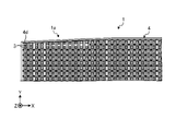
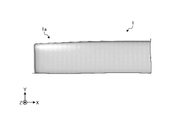
- FIG. 1 is a perspective view of a planar illumination device 1 according to the first embodiment.
- the longitudinal direction of the planar illumination device 1 is the X-axis direction
- the lateral direction is the Y-axis direction
- the thickness direction is the Z-axis direction.
- a planar illumination device 1 includes a substrate 2 and a reflector 4 fixed to the upper side of the substrate 2 in the drawing with double-sided tape or the like. Moreover, a notch 1a is provided on the left side of the substrate 2 and the reflector 4 in the drawing to form an irregular outer shape.
- the deformed external shape may be not only a linear chip like the notch portion 1a, but also an arc-shaped chip or a chip with a complicated shape.
- FIG. 2 is an exploded perspective view of the planar illumination device 1.
- light sources 3 such as LEDs (Light Emitting Diodes) are arranged two-dimensionally on a substrate 2, and wiring (not shown) to each light source 3 is also provided.
- the substrate 2 and the reflector 4 are flat, but the substrate 2 and the reflector 4 may have a curved surface such as a convex curved surface or a concave curved surface.
- two-dimensional arrangement means arrangement on a curved surface, for example, arrangement at a position represented by two independent coordinate axes on a curved surface such as cylindrical coordinates or spherical coordinates. do.
- the light source 3 has an optical axis in the normal direction of the substrate 2 .
- a portion of the substrate 2 that is not covered by the reflector 4 (a portion exposed through a hole 4b, which will be described later) or the entire surface of the substrate 2 is treated to increase light reflectance.
- the optical sheet includes a prism sheet (prism film), a brightness enhancement sheet (brightness enhancement film), a louver sheet (louver film), and the like.
- FIG. 3 is an enlarged perspective view of the vicinity of the notch 1a of the reflector 4.
- FIG. 4 is an enlarged perspective view of the vicinity of the notch 1a of the reflector 4 from another viewpoint.
- FIG. 5 is a view of the planar illumination device 1 near the notch 1a from the direction directly facing the emission surface.
- the reflector 4 has outer walls 4e, 4f, 4g, and 4h (the outer wall 4h is not shown) that serve as the outer peripheral portion.
- a concave portion 4n in FIG. 4 is a portion where a double-sided tape for attaching the reflector 4 to the substrate 2 is arranged.
- the reflector 4 has a segment 4d provided corresponding to each light source 3 (Fig. 2).
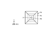
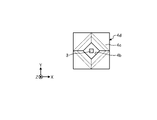
- the segment 4 d has a hole 4 b through which the head of the light source 3 is inserted, and a reflecting surface 4 c that extends obliquely from the periphery of the hole 4 b and surrounds the light source 3 .
- the segment 4d is formed in a rectangular shape, and the reflecting surface 4c is divided into four. That is, the light source 3 has a substantially rectangular outer shape in plan view, the predetermined shape of the segment is substantially rectangular in plan view, the hole 4b in the predetermined shape of the segment has a substantially rectangular outer shape in plan view,
- the reflecting surface 4c in the predetermined shape of the segment consists of four planes.
- part or all of the reflecting surface may be composed of two or more surfaces. For example, when all the reflecting surfaces are each composed of two surfaces, the total number of reflecting surfaces is eight.
- the cutout portion 1a having an irregular outer shape regarding the column of segments extending in the vertical direction at the left end of FIG.
- the segments are arranged in a non-predetermined shape.
- concave portions 4l and 4m for accommodating the light source 3 are provided on the surface of the outer wall 4g of the reflector 4 facing the substrate 2 (the back surface in FIG. 3).
- the recesses 4l, 4m are provided through the outer wall 4g and are of suitable width enough to accommodate the light sources 34, 35 (Fig. 5) even if the outer wall 4g is not thick enough. can be provided.
- segments are not arranged in the two rows from the top of the figure, and segments are arranged in the lower three rows, although they are not in a regular predetermined shape. ing.
- concave portions 4i, 4j, and 4k are provided on the surface of the outer wall 4g of the reflector 4 facing the substrate 2 (the back surface in FIG. 3). Two of the three recesses 4i, 4j are provided for accommodating light sources 31, 32 (Fig. 5). The remaining concave portion 4k is provided for adjusting the amount of light.
- the outer wall 4g does not interfere with the arrangement of the light source 33 (FIG. 5), but the area of the segment becomes smaller, and the amount of light per area increases and becomes brighter. Therefore, part of the light is consumed by the concave portion 4k to adjust the amount of light.
- the segments of the light source 36 (FIG. 5) also do not have a regular predetermined shape, but the recesses are not provided because the area of the segments is less reduced and the amount of light per area is less affected.
- the reflector 4 is made of, for example, a white resin having a high reflectance
- the material of the recesses 4i to 4m may be exposed as it is, or the reflectance may be changed by coloring or the like. .
- the portion where the light source 3 cannot be placed due to the outer wall 4g being in the way is By providing concave portions 4i, 4j, 4l, and 4m on the surface facing the substrate 2, the light sources 31, 32, 34, and 35 can be arranged, and the segments can be arranged. As a result, it is possible to prevent the luminance from being lowered in the peripheral portion of the deformed portion and to prevent the formation of a dark portion.
- the outer wall 4g does not interfere with the arrangement of the light source 33, but the concave portion 4k is used as described above for adjusting the amount of light per area.
- the concave portion 4l in the segment of the light source 34 is enlarged to the upper side of the figure. can do.
- the light from the light source 34 is guided to the area where the segment cannot be arranged and the area left halfway can be compensated for the lack of the amount of light.
- FIG. 6 is a perspective view showing an example in which the recesses 4i to 4m are provided without penetrating the outer wall 4g of the reflector 4.
- FIG. FIG. 6 is a view from the same viewpoint as FIG. In FIG. 6, since the outer wall 4g of the reflector 4 is thick, the recesses 4i, 4j, 4k, 4l, and 4m do not penetrate the outer wall 4g.
- the concave portions 4i, 4j, 4k, 4l, and 4m do not penetrate the outer wall 4g, the thickness of the outer wall 4g is maintained and the strength of the reflector 4 can be prevented from being lowered.
- Other effects are the same as those of the configuration example described above. Since there are spaces for arranging the light sources above the recess 4i in the drawing and above the recess 4l in the drawing, the segments and the recess may be provided in those portions. In that case, if the thickness of the outer wall 4g is insufficient, the recess may penetrate through the outer wall 4g as shown in FIG.
- the reflector 4 is arranged so that the non-emission side surface (lattice surface) of the reflector 4 is in contact with the substrate 2, but the outer walls 4e to 4h of the reflector 4 are in contact with the substrate 2. or only a part thereof, and the hole 4b of the segment 4d may be in a state of floating from the substrate 2.
- the head of the light source 3 arranged on the substrate 2 may or may not be inserted through the hole 4b of the segment 4d.
- the size of the hole 4b of the segment 4d in plan view is the light emitting portion of the light source 3 (for example, the inside of the rectangular outer shape of the light source 3). provided with a rectangular light-emitting portion), and may be smaller than the outer shape of the light source 3 .
- the reflector 4 can be easily manufactured by injection molding or the like, and the reflecting surfaces 4c of the segments 4d can be formed.
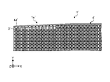
- FIG. 7 is a perspective view of the planar illumination device 1 according to the second embodiment.
- the longitudinal direction of the planar illumination device 1 is the X-axis direction
- the lateral direction is the Y-axis direction
- the thickness direction is the Z-axis direction.
- a planar illumination device 1 includes a substrate 2 and a reflector 4 fixed to the upper side of the substrate 2 in the drawing with double-sided tape or the like. 7, illustration of the light source (3) on the substrate 2 is omitted.
- a notch 1a is provided on the upper left side of the substrate 2 and the reflector 4 in the drawing to form an irregular outer shape.
- the deformed external shape may be not only a linear chip like the notch portion 1a, but also an arc-shaped chip or a chip with a complicated shape.
- FIG. 8 is an exploded perspective view of the planar illumination device 1.
- light sources 3 such as LEDs (Light Emitting Diodes) are arranged two-dimensionally on a substrate 2, and wiring (not shown) to each light source 3 is also provided.
- the substrate 2 and the reflector 4 are flat, but the substrate 2 and the reflector 4 may have a curved surface such as a convex curved surface or a concave curved surface.
- two-dimensional arrangement means arrangement on a curved surface, for example, arrangement at a position represented by two independent coordinate axes on a curved surface such as cylindrical coordinates or spherical coordinates. do.
- the light source 3 has an optical axis in the normal direction of the substrate 2 .
- a portion of the substrate 2 that is not covered by the reflector 4 (a portion exposed through a hole 4b, which will be described later) or the entire surface of the substrate 2 is treated to increase light reflectance.
- the optical sheet includes a prism sheet (prism film), a brightness enhancement sheet (brightness enhancement film), a louver sheet (louver film), and the like.
- FIG. 9 is an enlarged perspective view of the vicinity of the notch 1a of the reflector 4.
- FIG. 10A is a plan view showing the vicinity of the notch 1a of the planar illumination device 1.
- the reflector 4 has outer walls 4e, 4f, 4g, and 4h (the outer wall 4h is not shown) that serve as the outer peripheral portion.
- the reflector 4 has segments 4 d provided corresponding to the respective light sources 3 .
- the segment 4 d has a hole 4 b through which the head of the light source 3 is inserted, and a reflecting surface 4 c that extends obliquely from the periphery of the hole 4 b and surrounds the light source 3 .
- the outer walls 4e, 4f, 4g, and 4h do not need to be provided on the entire circumference of the outer peripheral portion, and may or may not be provided on a part thereof.
- the segment 4d is formed in a rectangular shape, and the reflecting surface 4c is divided into four.
- the light source 3 has a substantially cubic outer shape. That is, the light source 3 has a substantially rectangular outer shape in plan view, the standard shape of the segment excluding the deformed portion is substantially rectangular in plan view, and the hole 4b of the segment has a substantially rectangular outer shape in plan view.
- the reflecting surface 4c of the segment consists of four planes. In some cases, part or all of the reflecting surface may be composed of two or more surfaces. For example, when all the reflecting surfaces are each composed of two surfaces, the total number of reflecting surfaces is eight.
- the standard-shaped segment excluding the deformed portion is also referred to as a standard segment.
- a plurality of standard segments 4d are arranged regularly (in a grid) in the row and column directions.
- a segment group for improving uniformity is arranged instead of the standard segment. That is, in the 12 columns from the left end of the first row on the upper side of the figure to the right side, the two rows without the irregular shape are integrated by removing the partition wall in the middle.
- the irregular-shaped segment 4d and the segment 4d adjacent thereto are integrated by removing the partition wall (reflecting surface 4c) forming the boundary.
- the irregularly-shaped segment 4d is a (virtual) segment having at least one side along the outer shape of the whole (irregularly-shaped portion) and having a hole 4b smaller than the standard segment 4d.
- the light sources 3 are vertically spaced in the holes 4b of these segments 4d.
- the space where the partition wall (reflective surface 4c) was present can be used as a space for housing the light source 3.
- FIG. The other segment 4d is arranged so that the light emission center of the light source 3 is positioned at the center.
- the light emission center corresponds to the position of a minute light emitting chip built in the light source 3 and does not necessarily match the center of the package of the light source 3 .
- FIG. 10B is a diagram showing an example of luminance distribution of the planar illumination device 1 of FIG. 10A. Its characteristics will be described later.
- the number of the light sources 3 accommodated may be the same as that of the light sources 3 accommodated in the standard segment 4d. It does not have to be more than the number.
- the irregularly shaped segment 4d may be integrated with three or more segments 4d, or may not be integrated with the adjacent segment 4d.
- FIG. 11A is a plan view showing the vicinity of a notch 1a' of a planar illumination device 1' of a comparative example (modification).
- FIG. 11A in the planar illumination device 1′ of the comparative example, in the cutout portion 1a′, two rows of 12 columns toward the right side from the left end of the first row on the upper side are not deformed. It is the same as in FIG. 10A that the partition walls are removed and integrated.
- one light source 3' is placed in each original second row position in the hole of each segment 4d' of the profiled portion.
- FIG. 11B is a diagram showing an example of the luminance distribution of the planar illumination device 1' of FIG.
- the light sources 3 are densely arranged on the left side of the figure, where the brightness is slightly higher, but there is no dark area in the peripheral area.
- dark areas cannot be corrected, bright areas can be corrected by an optical sheet or the like arranged on the exit surface side of the reflector 4 .
- the luminance of the bright portion can be reduced and the overall luminance uniformity can be improved.
- the brightness of the bright portion can be reduced, and the uniformity of the overall brightness can be improved.
- FIG. 12A is a plan view showing the vicinity of the notch 1a of the planar illumination device 1 according to the third embodiment.
- the segments 4d arranged in a predetermined area (first to about fourth rows from the top) including the notch 1a having an irregular outer shape are uniform in shape and size.
- the predetermined area to be equalized is changed according to the mode of the deformed shape, and may be the entire surface or may be localized. Also, equalization does not mean that the shape and size are exactly the same, but that they are adjusted to be as similar as possible. Specifically, for example, in FIG.
- the size from the side of the upper end of the reflector 4 including the notch portion 1a to the upper end of the fifth line below excluding the width of the outer wall is divided into four equal parts, and there are four lines. segment 4d is arranged. Other configurations are the same as those in FIGS.
- FIG. 12B is a diagram showing an example of the luminance distribution of the planar illumination device 1 of FIG. 12A, and the luminance uniformity near the notch 1a is improved compared to the first embodiment of FIG. 10B.
- FIG. 13 is a perspective view showing the vicinity of the cutout portion 1a of the planar illumination device 1 according to the fourth embodiment, which is an improved version of the second embodiment shown in FIG. Note that similar improvements may be made to the third embodiment of FIG. 12A.
- the surface of the outer wall 4e facing the substrate 2 (the back surface in the figure) accommodates the light source 3, or the light source 3, similarly to the first embodiment.
- Concave portions 4i, 4j, 4k, and 4l are provided for adjusting the amount of light of 3.
- the recesses 4i, 4j, 4k, and 4l may or may not penetrate to the upper end of the outer wall 4e in the drawing.
- the reflector 4 is made of, for example, a white resin having a high reflectance.
- the recesses 4i, 4j, 4k, and 4l may be exposed as they are, or may be colored so that the reflectance of the surface is reduced. may be different.
- Other configurations are the same as those in FIGS.
- the size of the segment 4d cannot be sufficiently secured by the notch portion 1a, it may be difficult to arrange a plurality (two) of the light sources 3. Since the light source 3 can be arranged so as to hide the light source 3, it becomes easy to secure a space for arranging the light source 3. - ⁇ In addition, by arranging a plurality of (two) light sources 3 in the narrow segment 4d, the amount of light per area increases and the brightness increases (as described above in FIG.
- the outer wall 4e serves as a cover for the light source 3, which is partially inserted into 4k and 4l, and blocks the light emitted directly above, thereby suppressing the amount of light, resulting in an unnecessarily high luminance. can be prevented. As a result, luminance uniformity can be improved.
- FIG. 14 is a plan view of the planar illumination device 1 according to the fifth embodiment.
- the illustration of the outer wall of the reflector 4 is omitted. 7 and 8, the substrate 2 is provided behind the reflector 4, and the light source 3 is arranged on the substrate 2.
- FIG. 10A this is applied when a plurality of (two) light sources 3 are accommodated in the segment 4d on the notch 1a side, but one light source 3 is accommodated in the equalized segment 4d as shown in FIG. 12A. The same can be applied to the case where the light source 3 is accommodated.
- a plurality (two) of light sources 3 are housed in the segment 4d of the first row on the notch 1a side of the reflector 4, as in the second embodiment of FIG. 10A.
- the light sources 3 at the four corners of the reflector 4 as a whole are arranged with a rotation angle of 0° in which the four sides of the periphery are aligned with or perpendicular to the X-axis or the Y-axis in a plane parallel to the reflector 4 and the substrate (2). It has become.
- the light source 3 arranged between the corners of both ends in the segment 4d of the first row on the side of the notch 1a has its rotation angle changed continuously from the right corner.
- the other light sources 3 are arranged with a rotation angle of 45°.
- FIG. 15A is a plan view showing an example in which the rotation angle within the plane of the light source 3 of the planar illumination device 1 is 0°.
- the illustration of the outer wall of the reflector 4 is omitted.
- the light source 3 has a substantially cubic (or substantially rectangular parallelepiped) package outer shape, and emits light mainly from four side surfaces provided with phosphors. Therefore, the direction of light emission is anisotropic, and the amount of light in the front direction of each of the four side surfaces increases.
- the in-plane rotation angle of the light source 3 is 0°, the amount of light in the X-axis direction and the Y-axis direction increases.
- FIG. 15B is a diagram showing the characteristics of the luminance distribution in the arrangement of FIG. 15A, where the luminance is high in a region R1 where the corners of the four segments 4d congregate, causing non-uniform luminance.
- FIG. 16A is a plan view showing an example in which the rotation angle within the plane of the light source 3 of the planar illumination device 1 is 45°.
- the illustration of the outer wall of the reflector 4 is omitted.
- FIG. 16B is a diagram showing the characteristics of the luminance distribution in the case of the arrangement of FIG. 16A.
- brightness is lower.
- the brightness of the entire corner region R2 is reduced, causing non-uniform brightness. This is because the corners of the whole do not have segments adjacent to each other in two directions, so the brightness tends to be originally low.
- the corners of each segment 4d become bright, so that the decrease in luminance is alleviated, but in the arrangement of FIG.
- the rotation angle of the light sources 3 at the corners is set to 0° in order to suppress the decrease in luminance at the corners.
- the rotation angle of the light source 3 is set to 45° except for the notch 1a side so that the brightness of the portion where the corners of the four segments 4d gather does not become high.
- the light sources 3 arranged in the segment 4d except for the entire corners, which are both ends on the notch 1a side, are continuously changed in rotation angle from the light source 3 at the right end. This is because the area of the segment 4d is larger on the right side than on the left side, and the amount of light on the right side is relatively small. be.
- FIG. 17 is a plan view showing an example in which all the light sources 3 of the planar illumination device 1 have a rotation angle of 0° within the plane.
- the illustration of the outer wall of the reflector 4 is omitted.
- the decrease in luminance at the corners of the entirety is mitigated to some extent, but the luminance is increased at the corners of the four inner segments 4d, resulting in uniform luminance. diminished sexuality.
- FIG. 18 is a plan view showing an example in which all the light sources 3 of the planar illumination device 1 are rotated by 45 degrees within the plane.
- the illustration of the outer wall of the reflector 4 is omitted.
- the increase in luminance at the corners of the four inner segments 4d is suppressed, but the decrease in luminance at the corners as a whole becomes significant. , the brightness uniformity is degraded.
- FIG. 19 is a plane showing an example in which the rotation angle of the light source 3 in the plane of the entire corner of the planar illumination device 1 is 0° and the rotation angle of the other light source 3 in the plane is 45°. It is a diagram. The illustration of the outer wall of the reflector 4 is omitted. In this case, the decrease in luminance at the corners of the entirety is mitigated to some extent, and the increase in luminance at the corners of the four inner segments 4d is suppressed.
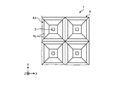
- FIG. 20 is a plan view showing an example of the shape of the reflecting surface 4c of the segment 4d of the reflector 4. As described above, the reflecting surfaces are formed by a plurality of planes divided by the diagonals of the rectangular segment 4d. 4c is configured. The dashed lines in the figure indicate the contour lines of the shape.
- FIG. 21 is a plan view showing another example of the shape of the reflecting surface 4c of the segment 4d of the reflector 4, in which the reflecting surface 4c is composed of a plurality of planes divided by vertical and horizontal crosshairs.
- the relative rotation angle between the anisotropy of the light source 3 and the anisotropy of the segment 4d is the same as in FIG. 16A, and the effect is also the same.
- FIG. 22 is a plan view showing another example of the shape of the reflecting surface 4c of the segment 4d of the reflector 4, in which the reflecting surface 4c is composed of a conical curved surface. In this case, the anisotropy of the segment 4d is eliminated or relaxed, leaving only the anisotropy of the light source 3.
- FIG. 22 is a plan view showing another example of the shape of the reflecting surface 4c of the segment 4d of the reflector 4, in which the reflecting surface 4c is composed of a conical curved surface. In this case, the anisotropy of the segment 4d is eliminated or relaxed, leaving only the anisotropy of the light source 3.
- FIG. 23 is a plan view showing another example of the shape of the reflective surface 4c of the segment 4d of the reflector 4.
- One area partitioned by one diagonal line is a plurality of planes divided by the other diagonal line, and the other area is divided by the other diagonal line.
- the reflecting surface 4c is formed by a conical curved surface.
- the anisotropy of the segment 4d disappears or is relaxed in the other region, leaving only the anisotropy of the light source 3.
- the luminance can be changed in various ways.
- the planar illumination device includes a plurality of light sources, a substrate on which the light sources are arranged two-dimensionally, holes corresponding to the light sources, and reflecting surfaces extending obliquely from the periphery of the holes.
- an outer wall is provided on the entire outer peripheral portion of the segment, and a reflector is arranged on the output side of the substrate, and is arranged in a deformed portion of the outer peripheral portion of the reflector, and the outer wall forms a predetermined shape.
- the surface of the outer wall facing the substrate is provided with a concave portion for accommodating the light source or adjusting the amount of light. As a result, even in the case of having an irregular outer shape, it is possible to prevent the occurrence of dark areas.
- the recess is provided through the outer wall. This makes it possible to provide a recess of suitable width sufficient to accommodate the light source even if the outer wall thickness is not sufficient.
- the recess is provided without penetrating the outer wall. Therefore, it is possible to cope with the case where the thickness of the outer wall is sufficient, and it is possible to prevent the strength of the reflector from being lowered.
- the light source has a substantially rectangular outer shape in plan view
- the predetermined shape of the segment is substantially rectangular in plan view
- the hole in the predetermined shape of the segment has a substantially rectangular outer shape in plan view.
- the reflective surface in the predetermined shape of the segment is composed of a plurality of planes.
- It also has a segment group for improving uniformity that is arranged in the deformed portion of the outer periphery of the reflector. Thereby, even if the display device has an irregular outer shape, it is possible to maintain luminance uniformity.
- the irregularly shaped segment and the segment adjacent to the segment are integrated by removing the boundary partition. This makes it possible to construct a segment suitable for an irregularly shaped portion. Also, the space for accommodating the light source can be increased.
- a segment having a plurality of light sources, a substrate on which the light sources are two-dimensionally arranged, holes corresponding to the light sources, and reflective surfaces extending obliquely from the periphery of the holes is provided. and a group of segments for uniformity improvement arranged on the deformed portion of the outer periphery of the reflector.
- the irregularly shaped segment and the segment adjacent to the segment are integrated by removing the boundary partition. This makes it possible to construct a segment suitable for an irregularly shaped portion. Also, the space for accommodating the light source can be increased.
- the present invention is not limited by the above-described embodiment.
- the present invention also includes those configured by appropriately combining the respective constituent elements described above. Further effects and modifications can be easily derived by those skilled in the art. Therefore, broader aspects of the present invention are not limited to the above-described embodiments, and various modifications are possible.
- 1 Planar illumination device 1a notch, 2 substrate, 3, 31 to 36 light source, 4 reflector, 4a base material, 4b hole, 4c reflecting surface, 4d segment, 4e to 4h outer wall, 4i to 4m recess
Landscapes
- Engineering & Computer Science (AREA)
- General Engineering & Computer Science (AREA)
- Planar Illumination Modules (AREA)
Priority Applications (4)
| Application Number | Priority Date | Filing Date | Title |
|---|---|---|---|
| CN202280032613.6A CN117280155A (zh) | 2021-06-28 | 2022-03-18 | 面状照明装置 |
| JP2023531428A JP7518977B2 (ja) | 2021-06-28 | 2022-03-18 | 面状照明装置 |
| EP22832491.9A EP4365488A4 (en) | 2021-06-28 | 2022-03-18 | PLAN LIGHTING DEVICE |
| US18/571,842 US20240360980A1 (en) | 2021-06-28 | 2022-03-18 | Planar illumination device |
Applications Claiming Priority (4)
| Application Number | Priority Date | Filing Date | Title |
|---|---|---|---|
| JP2021-106666 | 2021-06-28 | ||
| JP2021106666 | 2021-06-28 | ||
| JP2021139887 | 2021-08-30 | ||
| JP2021-139887 | 2021-08-30 |
Publications (1)
| Publication Number | Publication Date |
|---|---|
| WO2023276328A1 true WO2023276328A1 (ja) | 2023-01-05 |
Family
ID=84692611
Family Applications (1)
| Application Number | Title | Priority Date | Filing Date |
|---|---|---|---|
| PCT/JP2022/012691 Ceased WO2023276328A1 (ja) | 2021-06-28 | 2022-03-18 | 面状照明装置 |
Country Status (4)
| Country | Link |
|---|---|
| US (1) | US20240360980A1 (https=) |
| EP (1) | EP4365488A4 (https=) |
| JP (1) | JP7518977B2 (https=) |
| WO (1) | WO2023276328A1 (https=) |
Cited By (2)
| Publication number | Priority date | Publication date | Assignee | Title |
|---|---|---|---|---|
| US12510706B2 (en) | 2023-09-26 | 2025-12-30 | Lextar Electronics Corporation | Optical module |
| TWI911897B (zh) * | 2023-09-26 | 2026-01-11 | 隆達電子股份有限公司 | 光學模組 |
Citations (3)
| Publication number | Priority date | Publication date | Assignee | Title |
|---|---|---|---|---|
| JP2011089121A (ja) * | 2009-10-23 | 2011-05-06 | Samsung Led Co Ltd | 赤色蛍光体、赤色蛍光体の製造方法、発光素子パッケージ、面光源装置、照明装置及び車両用ヘッドライト |
| JP2019091036A (ja) * | 2017-11-13 | 2019-06-13 | エルジー ディスプレイ カンパニー リミテッド | 異形液晶発光装置 |
| JP2021012884A (ja) | 2019-03-08 | 2021-02-04 | 日亜化学工業株式会社 | 光源装置 |
Family Cites Families (9)
| Publication number | Priority date | Publication date | Assignee | Title |
|---|---|---|---|---|
| US6923557B2 (en) * | 2003-10-21 | 2005-08-02 | Lightshapes Inc. | Modular lighting assembly |
| WO2006003913A1 (ja) * | 2004-07-06 | 2006-01-12 | Asagicreate Co., Ltd. | 面状光源および電飾看板 |
| US7517105B2 (en) * | 2006-01-06 | 2009-04-14 | Asagicreate Co., Ltd. | Surface light source and electrically illuminated signboard |
| US7828456B2 (en) * | 2007-10-17 | 2010-11-09 | Lsi Industries, Inc. | Roadway luminaire and methods of use |
| JP2011034674A (ja) * | 2008-02-05 | 2011-02-17 | Asagi Create:Kk | 面状光源および電飾看板 |
| FR3053757B1 (fr) * | 2016-07-05 | 2020-07-17 | Valeo Vision | Dispositif d'eclairage et/ou de signalisation pour vehicule automobile |
| TWI854915B (zh) * | 2019-03-08 | 2024-09-01 | 日商日亞化學工業股份有限公司 | 光源裝置 |
| US20240231146A1 (en) * | 2020-03-19 | 2024-07-11 | Enplas Corporation | Light flux controlling member, light emitting device, surface light source device and display device |
| US20220308272A1 (en) * | 2021-03-24 | 2022-09-29 | Nichia Corporation | Light-reflecting member and light source device |
-
2022
- 2022-03-18 US US18/571,842 patent/US20240360980A1/en active Pending
- 2022-03-18 JP JP2023531428A patent/JP7518977B2/ja active Active
- 2022-03-18 EP EP22832491.9A patent/EP4365488A4/en active Pending
- 2022-03-18 WO PCT/JP2022/012691 patent/WO2023276328A1/ja not_active Ceased
Patent Citations (3)
| Publication number | Priority date | Publication date | Assignee | Title |
|---|---|---|---|---|
| JP2011089121A (ja) * | 2009-10-23 | 2011-05-06 | Samsung Led Co Ltd | 赤色蛍光体、赤色蛍光体の製造方法、発光素子パッケージ、面光源装置、照明装置及び車両用ヘッドライト |
| JP2019091036A (ja) * | 2017-11-13 | 2019-06-13 | エルジー ディスプレイ カンパニー リミテッド | 異形液晶発光装置 |
| JP2021012884A (ja) | 2019-03-08 | 2021-02-04 | 日亜化学工業株式会社 | 光源装置 |
Non-Patent Citations (1)
| Title |
|---|
| See also references of EP4365488A4 |
Cited By (2)
| Publication number | Priority date | Publication date | Assignee | Title |
|---|---|---|---|---|
| US12510706B2 (en) | 2023-09-26 | 2025-12-30 | Lextar Electronics Corporation | Optical module |
| TWI911897B (zh) * | 2023-09-26 | 2026-01-11 | 隆達電子股份有限公司 | 光學模組 |
Also Published As
| Publication number | Publication date |
|---|---|
| US20240360980A1 (en) | 2024-10-31 |
| JPWO2023276328A1 (https=) | 2023-01-05 |
| JP7518977B2 (ja) | 2024-07-18 |
| EP4365488A4 (en) | 2025-07-02 |
| EP4365488A1 (en) | 2024-05-08 |
Similar Documents
| Publication | Publication Date | Title |
|---|---|---|
| JP5920616B2 (ja) | 直下型ledバックライト装置及びそれを用いた液晶表示装置 | |
| US7901102B2 (en) | Backlight unit and liquid crystal display apparatus employing the same | |
| TWI422782B (zh) | 照明系統,照明器及背光單元 | |
| US8950884B2 (en) | Backlight and display | |
| JP4507062B2 (ja) | 面光源装置及び当該装置を用いた機器 | |
| US20080094853A1 (en) | Light guides and backlight systems incorporating light redirectors at varying densities | |
| US10032963B2 (en) | Light emitting diode package module and display device having the same | |
| US20180107068A1 (en) | Backlight device and liquid crystal display device | |
| US20110051044A1 (en) | Light quantity control member, surface light source unit and display device | |
| US9207382B2 (en) | Light unit having light guide member with receiving holes with round part | |
| JP2019515459A (ja) | 照明モジュール及びこれを備える照明装置 | |
| JPWO2009110145A1 (ja) | 発光素子、照明装置および液晶表示装置 | |
| CN101688647A (zh) | 照明装置和液晶显示装置 | |
| WO2023276328A1 (ja) | 面状照明装置 | |
| US20180239197A1 (en) | Backlight device and liquid crystal display apparatus | |
| US8297824B2 (en) | Light guide plate and display device using the same | |
| US7989829B2 (en) | Light emitting diode backlight module and liquid crystal display | |
| CN117280155A (zh) | 面状照明装置 | |
| US20230184405A1 (en) | Flat lamp and lighting module thereof | |
| CN215730563U (zh) | 背光模组及显示装置 | |
| JP7307009B2 (ja) | 面状照明装置 | |
| JP7580048B2 (ja) | 導光板、及び、照明装置 | |
| US7347601B2 (en) | Vehicle lamp unit | |
| JP6751452B2 (ja) | 面状照明装置 | |
| JP2017130379A (ja) | 照明装置 |
Legal Events
| Date | Code | Title | Description |
|---|---|---|---|
| 121 | Ep: the epo has been informed by wipo that ep was designated in this application |
Ref document number: 22832491 Country of ref document: EP Kind code of ref document: A1 |
|
| WWE | Wipo information: entry into national phase |
Ref document number: 2023531428 Country of ref document: JP |
|
| WWE | Wipo information: entry into national phase |
Ref document number: 202280032613.6 Country of ref document: CN |
|
| WWE | Wipo information: entry into national phase |
Ref document number: 2022832491 Country of ref document: EP |
|
| NENP | Non-entry into the national phase |
Ref country code: DE |
|
| ENP | Entry into the national phase |
Ref document number: 2022832491 Country of ref document: EP Effective date: 20240129 |