WO2023243556A1 - 電界効果トランジスタ - Google Patents
電界効果トランジスタ Download PDFInfo
- Publication number
- WO2023243556A1 WO2023243556A1 PCT/JP2023/021506 JP2023021506W WO2023243556A1 WO 2023243556 A1 WO2023243556 A1 WO 2023243556A1 JP 2023021506 W JP2023021506 W JP 2023021506W WO 2023243556 A1 WO2023243556 A1 WO 2023243556A1
- Authority
- WO
- WIPO (PCT)
- Prior art keywords
- gate structure
- source
- layer
- wiring
- nitride semiconductor
- Prior art date
- Legal status (The legal status is an assumption and is not a legal conclusion. Google has not performed a legal analysis and makes no representation as to the accuracy of the status listed.)
- Ceased
Links
Images


Classifications
-
- H—ELECTRICITY
- H10—SEMICONDUCTOR DEVICES; ELECTRIC SOLID-STATE DEVICES NOT OTHERWISE PROVIDED FOR
- H10D—INORGANIC ELECTRIC SEMICONDUCTOR DEVICES
- H10D30/00—Field-effect transistors [FET]
- H10D30/01—Manufacture or treatment
- H10D30/051—Manufacture or treatment of FETs having PN junction gates
-
- H—ELECTRICITY
- H10—SEMICONDUCTOR DEVICES; ELECTRIC SOLID-STATE DEVICES NOT OTHERWISE PROVIDED FOR
- H10D—INORGANIC ELECTRIC SEMICONDUCTOR DEVICES
- H10D30/00—Field-effect transistors [FET]
- H10D30/01—Manufacture or treatment
- H10D30/061—Manufacture or treatment of FETs having Schottky gates
-
- H—ELECTRICITY
- H10—SEMICONDUCTOR DEVICES; ELECTRIC SOLID-STATE DEVICES NOT OTHERWISE PROVIDED FOR
- H10D—INORGANIC ELECTRIC SEMICONDUCTOR DEVICES
- H10D30/00—Field-effect transistors [FET]
- H10D30/40—FETs having zero-dimensional [0D], one-dimensional [1D] or two-dimensional [2D] charge carrier gas channels
- H10D30/47—FETs having zero-dimensional [0D], one-dimensional [1D] or two-dimensional [2D] charge carrier gas channels having two-dimensional [2D] charge carrier gas channels, e.g. nanoribbon FETs or high electron mobility transistors [HEMT]
-
- H—ELECTRICITY
- H10—SEMICONDUCTOR DEVICES; ELECTRIC SOLID-STATE DEVICES NOT OTHERWISE PROVIDED FOR
- H10D—INORGANIC ELECTRIC SEMICONDUCTOR DEVICES
- H10D30/00—Field-effect transistors [FET]
- H10D30/80—FETs having rectifying junction gate electrodes
- H10D30/83—FETs having PN junction gate electrodes
-
- H—ELECTRICITY
- H10—SEMICONDUCTOR DEVICES; ELECTRIC SOLID-STATE DEVICES NOT OTHERWISE PROVIDED FOR
- H10D—INORGANIC ELECTRIC SEMICONDUCTOR DEVICES
- H10D30/00—Field-effect transistors [FET]
- H10D30/80—FETs having rectifying junction gate electrodes
- H10D30/87—FETs having Schottky gate electrodes, e.g. metal-semiconductor FETs [MESFET]
-
- H—ELECTRICITY
- H10—SEMICONDUCTOR DEVICES; ELECTRIC SOLID-STATE DEVICES NOT OTHERWISE PROVIDED FOR
- H10D—INORGANIC ELECTRIC SEMICONDUCTOR DEVICES
- H10D62/00—Semiconductor bodies, or regions thereof, of devices having potential barriers
- H10D62/80—Semiconductor bodies, or regions thereof, of devices having potential barriers characterised by the materials
- H10D62/83—Semiconductor bodies, or regions thereof, of devices having potential barriers characterised by the materials being Group IV materials, e.g. B-doped Si or undoped Ge
-
- H—ELECTRICITY
- H10—SEMICONDUCTOR DEVICES; ELECTRIC SOLID-STATE DEVICES NOT OTHERWISE PROVIDED FOR
- H10D—INORGANIC ELECTRIC SEMICONDUCTOR DEVICES
- H10D64/00—Electrodes of devices having potential barriers
- H10D64/20—Electrodes characterised by their shapes, relative sizes or dispositions
-
- H—ELECTRICITY
- H10—SEMICONDUCTOR DEVICES; ELECTRIC SOLID-STATE DEVICES NOT OTHERWISE PROVIDED FOR
- H10D—INORGANIC ELECTRIC SEMICONDUCTOR DEVICES
- H10D64/00—Electrodes of devices having potential barriers
- H10D64/20—Electrodes characterised by their shapes, relative sizes or dispositions
- H10D64/23—Electrodes carrying the current to be rectified, amplified, oscillated or switched, e.g. sources, drains, anodes or cathodes
-
- H—ELECTRICITY
- H10—SEMICONDUCTOR DEVICES; ELECTRIC SOLID-STATE DEVICES NOT OTHERWISE PROVIDED FOR
- H10D—INORGANIC ELECTRIC SEMICONDUCTOR DEVICES
- H10D64/00—Electrodes of devices having potential barriers
- H10D64/20—Electrodes characterised by their shapes, relative sizes or dispositions
- H10D64/27—Electrodes not carrying the current to be rectified, amplified, oscillated or switched, e.g. gates
Definitions
- the present disclosure relates to field effect transistors.
- HEMTs high electron mobility transistors
- FETs field effect transistors
- GaN gallium nitride
- 2DEG two-dimensional electron gas
- Power transistors using HEMTs are recognized as devices that have lower on-resistance and can operate at higher speeds and higher frequencies than typical silicon (Si) power transistors.
- the gate capacitance of a HEMT is relatively small for a power transistor, surges caused by static electricity or the like may not be sufficiently absorbed within the device.
- the semiconductor wafer is mechanically cut by rotating a blade at high speed, so that surges are likely to enter the transistors. If the surge resistance is low, the surge may cause deterioration of transistor characteristics such as an increase in on-resistance and a decrease in breakdown voltage.
- a transistor is formed in the active region where 2DEG occurs. Therefore, there is still room for improvement in improving resistance to surges that can invade the active region.
- a field effect transistor includes a substrate, a first nitride semiconductor layer disposed above the substrate, and a first nitride semiconductor layer having a larger band gap than the first nitride semiconductor layer; a second nitride semiconductor layer disposed on the first nitride semiconductor layer to generate a two-dimensional electron gas in the first nitride semiconductor layer near the interface with the semiconductor layer; A source electrode, a drain electrode, and a gate structure are provided on a nitride semiconductor layer.
- the first nitride semiconductor layer includes an active region where the two-dimensional electron gas is generated, and an inactive region surrounding the active region in plan view.
- the source electrode, the drain electrode, and the gate structure are disposed on the second nitride semiconductor layer in a region corresponding to the active region.
- the source electrode surrounds the drain electrode and the gate structure in plan view, and extends along the outer periphery of the second nitride semiconductor layer corresponding to the boundary between the active region and the inactive region. Includes the outer periphery of the source contact in contact with the layer.
- a field effect transistor according to one embodiment of the present disclosure can improve surge resistance.
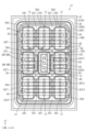
- FIG. 1 is a schematic plan view of an exemplary field effect transistor according to a first embodiment.
- FIG. 2 is a schematic cross-sectional view taken along line F2-F2 in FIG.
- FIG. 3 is a schematic plan view showing an exemplary upper wiring structure of the field effect transistor of FIG.
- FIG. 4 is a schematic plan view of an exemplary field effect transistor according to a second embodiment.
- FIG. 5 is a schematic plan view of an exemplary field effect transistor according to a third embodiment.
- FIG. 6 is a schematic plan view of an exemplary field effect transistor according to the fourth embodiment.
- FIG. 7 is a schematic plan view of an exemplary field effect transistor according to the fifth embodiment.
- FIG. 8 is a schematic plan view of an exemplary field effect transistor according to the sixth embodiment.
- FIG. 1 is a schematic plan view of an exemplary field effect transistor according to a first embodiment.
- FIG. 2 is a schematic cross-sectional view taken along line F2-F2 in FIG.
- FIG. 3 is a schematic plan
- FIG. 9 is a schematic cross-sectional view taken along line F9-F9 in FIG.
- FIG. 10 is a schematic plan view of an exemplary field effect transistor according to the seventh embodiment.
- FIG. 11 is a schematic plan view of an exemplary field effect transistor according to the eighth embodiment.
- FIG. 12 is a schematic plan view of an exemplary field effect transistor according to the ninth embodiment.
- FIG. 13 is a schematic cross-sectional view taken along line F13-F13 in FIG. 12.
- FIG. 14 is a schematic plan view of an exemplary field effect transistor according to the tenth embodiment.
- FIG. 15 is a schematic plan view of an exemplary field effect transistor according to the eleventh embodiment.
- FIG. 1 is a schematic plan view of an exemplary field effect transistor (FET) 10 according to a first embodiment.
- FIG. 2 is a schematic cross-sectional view of the FET 10 taken along line F2-F2 in FIG.
- FET 10 may be configured as a high electron mobility transistor (HEMT) using a nitride semiconductor.
- HEMT high electron mobility transistor
- Typical examples of nitride semiconductors are gallium nitride (GaN), aluminum nitride (AlN), and indium nitride (InN), and generally Al x In y Ga 1-x-y N (0 ⁇ x ⁇ 1,0 ⁇ y ⁇ 1, 0 ⁇ x+y ⁇ 1).
- planar view refers to the object (FET 10 or its components) in the Z direction of the mutually orthogonal XYZ axes shown in each figure, unless explicitly stated otherwise. It means to see.
- the Y direction may be referred to as a first direction
- the X direction may be referred to as a second direction.
- the +Z direction is sometimes referred to as top, the -Z direction as bottom, the +X direction as right, and the -X direction as left.
- the FET 10 includes a plurality of (four in the example of FIG. 1) FET cells 12A, 12B, 12C, and 12D.
- FET cells 12A, 12B, 12C, and 12D are collectively referred to as the FET cell 12.
- the FET 10 is shown as including four FET cells 12; however, the FET 10 may include, for example, tens to hundreds of FET cells 12 to provide It can be configured as a transistor (power switching FET).
- the FET cell 12A includes FET elements 14A1 and 14A2.
- FET cell 12B includes FET elements 14B1 and 14B2
- FET cell 12C includes FET elements 14C1 and 14C2
- FET cell 12D includes FET elements 14D1 and 14D2.
- FET elements 14A1, 14A2, 14B1, 14B2, 14C1, 14C2, 14D1, and 14D2 are not distinguished from each other, they will be collectively referred to as FET elements 14.
- Each FET element 14 is part of a transistor structure (HEMT in the example of FIGS. 1 and 2) that contributes to the operation of FET 10.
- FIG. 2 shows the structure of the FET cell 12A along line F2-F2 in FIG. 1 and its surrounding structure.
- an exemplary cross-sectional structure of the FET element 14 will first be described with reference to FIG. 2. Note that the cross-sectional structure of the FET element 14 is the same for each FET cell 12.
- the FET 10 includes a substrate 22, a buffer layer 24 formed on the substrate 22, an electron transport layer 26 formed on the buffer layer 24, and an electron supply layer 28 formed on the electron transport layer 26.
- Substrate 22 may be formed of silicon (Si), silicon carbide (SiC), GaN, sapphire, or other substrate material.
- the substrate 22 is a conductive Si substrate.
- the thickness of the substrate 22 may be, for example, 200 ⁇ m or more and 1500 ⁇ m or less. Note that the Z direction shown in each figure is a direction perpendicular to the main surface of the substrate 22.
- the buffer layer 24 is located between the substrate 22 and the electron transport layer 26, and is made of any suitable material capable of suppressing wafer warping and cracking due to mismatching of thermal expansion coefficients between the substrate 22 and the electron transport layer 26. It can be formed by any material.
- Buffer layer 24 may include one or more nitride semiconductor layers.
- buffer layer 24 may include at least one of an aluminum nitride (AlN) layer, an aluminum gallium nitride (AlGaN) layer, and a graded AlGaN layer having a different aluminum (Al) composition.
- the buffer layer 24 may be formed by a single AlN layer, a single AlGaN layer, a layer having an AlGaN/GaN superlattice structure, a layer having an AlN/AlGaN superlattice structure, or a layer having an AlN/GaN superlattice structure. can be formed.
- buffer layer 24 includes a first buffer layer formed on substrate 22 and a second buffer layer formed on the first buffer layer.
- the first buffer layer is, for example, an AlN layer, and may have a thickness of, for example, about 200 nm.
- the second buffer layer may include, for example, a plurality of AlGaN layers, and each AlGaN layer may have a thickness of, for example, about 100 nm.
- impurities may be introduced into a part of the buffer layer 24 to make it semi-insulating.
- the impurity is, for example, carbon (C) or iron (Fe), and the concentration of the impurity may be, for example, 4 ⁇ 10 16 cm ⁇ 3 or more.
- Electron transit layer 26 may be formed of a nitride semiconductor.
- the electron transit layer 26 corresponds to the first nitride semiconductor layer.
- electron transit layer 26 may be a GaN layer.
- the thickness of the electron transit layer 26 may be, for example, 0.1 ⁇ m or more and 2 ⁇ m or less.
- impurities may be introduced into a part of the electron transit layer 26 to make the region other than the surface layer of the electron transit layer 26 semi-insulating.
- the impurity is, for example, C
- the concentration of the impurity may be, for example, 1 ⁇ 10 19 cm ⁇ 3 or more in peak concentration.
- Electron supply layer 28 may be formed of a nitride semiconductor. Electron supply layer 28 corresponds to the second nitride semiconductor layer.
- electron supply layer 28 may be an AlGaN layer. In the AlGaN layer, the band gap increases as the Al composition increases. Therefore, the electron supply layer 28, which is an AlGaN layer, has a larger band gap than the electron transit layer 26, which is a GaN layer.
- the electron supply layer 28 is made of Al x Ga 1-x N, where x is in the range of 0.1 ⁇ x ⁇ 0.4, more preferably 0.2 ⁇ x ⁇ 0.3. However, it is not necessarily limited to this range.
- the thickness of the electron supply layer 28 may be, for example, 5 nm or more and 20 nm or less.
- the electron transit layer 26 and the electron supply layer 28 are made of nitride semiconductors having different lattice constants. Therefore, the nitride semiconductor (eg, GaN) forming the electron transit layer 26 and the nitride semiconductor (eg, AlGaN) forming the electron supply layer 28 form a lattice-mismatched junction. Due to the spontaneous polarization of the electron transit layer 26 and the electron supply layer 28 and the piezo polarization caused by the stress applied to the heterojunction of the electron supply layer 28, electrons near the heterojunction interface between the electron transit layer 26 and the electron supply layer 28 are The energy level of the conduction band of the traveling layer 26 is lower than the Fermi level.
- two-dimensional electron gas (2DEG) 30 spreads within the electron transit layer 26 at a position close to the heterojunction interface between the electron transit layer 26 and the electron supply layer 28 (for example, at a distance of several nm from the interface). There is.
- the electron transit layer 26 includes an active region 26R1 in which 2DEG 30 can be generated, and an inactive region 26R2 surrounding the active region 26R1 in plan view.
- the non-active region 26R2 is formed, for example, by removing the upper outer circumference of the electron transit layer 26 together with the outer circumference of the electron supply layer 28 located directly above it. Therefore, the electron transit layer 26 includes a side surface 26S1 at the boundary between the active region 26R1 and the non-active region 26R2, and the electron supply layer 28 includes a side surface 28S1 formed continuously with the side surface 26S1 of the electron transit layer 26. .
- the side surface 28S1 of the electron supply layer 28 coincides with the side surface 26S1 of the electron transit layer 26 in plan view.
- the side surface 26S1 of the electron transit layer 26 is provided as a step wall that forms a step between the active region 26R1 and the non-active region 26R2.
- the side surface 28S1 of the electron supply layer 28 and the side surface 26S1 of the electron transit layer 26 are formed as vertical surfaces, but they are inclined outward from the upper end of the side surface 28S1 to the lower end of the side surface 26S1. It may also be formed as a surface.
- the electron transit layer 26 includes an outer peripheral end surface 26S2 at the outer peripheral end of the chip of the FET 10. Therefore, the non-active region 26R2 corresponds to the region of the electron transit layer 26 between the outer peripheral end surface 26S2 and the side surface 26S1. In the example of FIG. 2, non-active region 26R2 corresponds to a region of electron transit layer 26 over which electron supply layer 28 is not present. Therefore, 2DEG30 is not generated in the non-active region 26R2.
- the non-active region 26R2 is formed along the outer peripheral end surface 26S2 of the electron transit layer 26 in plan view (see FIG. 1).
- the active region 26R1 corresponds to a region of the electron transit layer 26 that is inside the non-active region 26R2 in plan view.
- active region 26R1 corresponds to the region of electron transit layer 26 over which electron supply layer 28 is present (thereby allowing generation of 2DEG 30).
- the inactive region 26R2 can be formed by, for example, using an etching method to remove the outer circumference of the electron supply layer 28 and the upper outer circumference of the electron transit layer 26 located directly below it.
- the non-active region 26R2 is not limited to being formed using an etching method.
- the inactive region 26R2 may be formed by using an ion implantation method to increase the resistance of the outer circumference of the electron supply layer 28 and the upper outer circumference of the electron transit layer 26 located directly below it.
- the etching method can be implemented at a lower cost than the ion implantation method, it is advantageous to use the etching method from the viewpoint of cost.
- FET 10 further includes a source electrode 32, a drain electrode 34, and a gate structure 36 disposed over electron supply layer 28.
- FET 10 also includes a passivation layer 38 disposed over electron supply layer 28 to cover gate structure 36 .
- the passivation layer 38 is made of, for example, a silicon nitride (SiN) film, a silicon dioxide (SiO 2 ) film, a silicon oxynitride (SiON) film, an alumina (Al 2 O 3 ) film, an AlN film, and an aluminum oxynitride (AlON) film. It is composed of a single film of any one of these or a composite film containing any combination of two or more thereof.
- the source electrode 32 and the drain electrode 34 are in ohmic contact with the 2DEG 30 generated in the electron transit layer 26 directly below the electron supply layer 28, that is, electrically connected to the 2DEG 30.
- the source electrode 32 and the drain electrode 34 are made of, for example, at least one of a titanium (Ti) layer, a titanium nitride (TiN) layer, an Al layer, an aluminum silicon copper (AlSiCu) layer, and an aluminum copper (AlCu) layer. may be formed by one or more metal layers.
- the source electrode 32 and the drain electrode 34 may be formed of the same metal material, or may be formed of different metal materials. When the source electrode 32 and the drain electrode 34 are formed of the same metal material, it is advantageous in that both can be formed in the same process.
- the cross-sectional shapes of the source electrode 32 and the drain electrode 34 are not particularly limited.
- the source electrode 32 and the drain electrode 34 can be formed by forming one or more metal layers on the passivation layer 38 so as to fill the openings 38A and 38B in the passivation layer 38, and then etching the metal layer. can be formed.
- the source electrode 32 and the drain electrode 34 may each have a substantially T-shape or a substantially Y-shape in a cross section along the ZX plane of FIG.
- the source electrode 32 may include a source electrode portion 32A and a source field plate portion 32B continuous with the source electrode portion 32A.
- the source electrode section 32A includes a filling region filled in the opening 38A of the passivation layer 38, and an upper region formed integrally with the filling region.
- the source field plate portion 32B is formed integrally with the upper region of the source electrode portion 32A, and is provided on the passivation layer 38 so as to cover the gate structure 36 in plan view.
- the source field plate section 32B is configured to extend the depletion layer toward the 2DEG 30 directly below the source field plate section 32B when a high voltage is applied between the source and the drain when the gate-source voltage is 0V. It serves to alleviate the electric field concentration near the ends of the structure 36.
- Gate structure 36 includes a gate layer 36A disposed on electron supply layer 28 and a gate electrode 36B disposed on gate layer 36A.
- the gate layer 36A may be formed of a nitride semiconductor having a smaller bandgap than the electron supply layer 28.
- the gate layer 36A may be a GaN layer doped with acceptor type impurities, that is, a p-type GaN layer.
- the acceptor type impurity may be, for example, at least one of zinc (Zn), magnesium (Mg), and carbon (C).
- the maximum concentration of acceptor type impurities in the gate layer 36A is, for example, 7 ⁇ 10 18 cm ⁇ 3 or more and 1 ⁇ 10 20 cm ⁇ 3 or less.
- the gate layer 36A is formed of a nitride semiconductor containing acceptor-type impurities, at zero bias when no voltage is applied to the gate electrode 36B, 2DEG 30 in the region directly under the gate layer 36A is depleted, thereby forming a conductive path. (channel) is blocked. As a result, a normally-off type HEMT in which the threshold voltage has a positive value is realized.
- the thickness of the gate layer 36A is not particularly limited, but can be appropriately determined in consideration of various parameters such as gate breakdown voltage.
- the thickness of the gate layer 36A may be greater than or equal to 80 nm and less than or equal to 150 nm.
- the cross-sectional shape of the gate layer 36A is not particularly limited.
- the gate layer 36A may have, for example, a rectangular shape, a trapezoidal shape, a ridge shape, or any other arbitrary shape in a cross section along the ZX plane in FIG. 2 .
- the gate electrode 36B may be formed of one or more metal layers.
- the gate electrode 36B is in Schottky junction or ohmic contact with the gate layer 36A.
- gate electrode 36B may be a titanium nitride (TiN) layer.
- the gate electrode 36B forms a Schottky junction with the gate layer 36A.
- the gate electrode 36B may be composed of a first metal layer (for example, a Ti layer) and a second metal layer (for example, a TiN layer) provided on the first metal layer.
- the thickness of the gate electrode 36B may be, for example, 50 nm or more and 300 nm or less.
- the gate electrode 36B is arranged on a part of the upper surface of the gate layer 36A, and has a width smaller than that of the gate layer 36A in the X direction.
- Such a gate structure 36 is advantageous in reducing gate leakage current compared to a case where the gate electrode 36B is formed to have the same width as the gate layer 36A in the X direction.
- the gate electrode 36B may be formed with the same width as the gate layer 36A.
- FET 10 further includes an interlayer insulating layer 42 that covers passivation layer 38 along with source electrode 32 and drain electrode 34, and a source wiring 44, drain wiring 46, and gate wiring 48 arranged on interlayer insulating layer 42.
- interlayer insulating layer 42 may be formed of silicon dioxide (SiO 2 ) or other insulating material, for example.
- SiO 2 silicon dioxide
- FIG. 2 shows a case where the surface is flat, it does not necessarily have to be flat.
- the interlayer insulating layer 42 may be formed with the same thickness within the region of the FET 10 so as to reflect the unevenness of the lower part of the interlayer insulating layer 42. Note that the passivation layer 38 and the interlayer insulating layer 42 can be collectively referred to as an insulating layer.
- the source wiring 44, the drain wiring 46, and the gate wiring 48 may be formed of a metal material such as gold (Au), Cu, or Al.
- the drain electrode 34 includes a plurality of (four in the example of FIG. 1) drain contact portions 34C1, 34C2, 34C3, and 34C4 that are in contact with the electron supply layer 28 (see FIG. 2).
- the drain contact portions 34C1 to 34C4 are arranged apart from each other in a first direction (Y direction) and a second direction (X direction) orthogonal to the first direction when viewed from above.
- Y direction first direction
- X direction second direction
- the drain contact portion 34C is a portion of the drain electrode 34 that contacts the electron supply layer 28 in the active region 26R1. Note that, in order to avoid complication of illustration, portions of the drain electrode 34 other than the drain contact portion 34C are not shown in FIG. Further, in order to facilitate understanding, the drain contact portion 34C is shown by hatching lines in FIG. Each drain contact portion 34C has a finger shape, that is, an elongated shape extending in the first direction.
- the gate structure 36 includes a plurality of (four in the example of FIG. 1) gate portions 36G1, 36G2, 36G3, and 36G4. Each of the gate portions 36G1, 36G2, 36G3, and 36G4 is provided so as to annularly surround a corresponding one of the drain contact portions 34C1, 34C2, 34C3, and 34C4. In the following description, when the gate sections 36G1 to 36G4 are not distinguished from each other, they are collectively referred to as the gate section 36G.
- Each gate portion 36G includes the gate layer 36A and gate electrode 36B described with reference to FIG. Note that the gate layer 36A is not shown in FIG. 1 to avoid complication of illustration. Further, in order to facilitate understanding, the gate electrode 36B is shown by hatching lines in FIG. In each gate portion 36G, the gate layer 36A and the gate electrode 36B are formed in an annular shape.
- an “annular” as used in this disclosure refers not only to any structure that forms a continuous shape or loop without an end, but also generally to a loop having a gap, such as a C-shape. It also refers to the structure of the shape.
- explicit reference to a "closed ring” refers to any structure that forms a continuous shape or loop with no ends, whereas explicit reference to an “open ring” generally refers to a loop that has a discontinuity.
- Such “annular” shapes can include not only elliptical shapes, but also any shape that includes multiple corners, with right angle corners or rounded corners.
- each gate portion 36G is formed in a closed annular shape.
- each gate portion 36G is not necessarily limited to a closed annular shape, but may be an open annular shape.
- each annular gate portion 36G includes a pair of gate structure finger portions 36F1 and 36F2 that are arranged in the formation region of the FET element 14 and extend in parallel to the first direction (Y direction).
- each gate portion 36G may be formed in an open annular shape having a cut at a position apart from the pair of gate structure finger portions 36F1 and 36F2.
- the gate parts 36G adjacent in the first direction (Y direction) are electrically connected to each other by a connecting part 37.
- the gate portion 36G1 and the gate portion 36G3 are electrically connected by the connecting portion 37
- the gate portion 36G2 and the gate portion 36G4 are electrically connected by the connecting portion 37.
- the connecting portion 37 may have a width larger than the width of the gate electrode 36B in each of the first direction (Y direction) and the second direction (X direction). Gate portions 36G adjacent in the second direction (X direction) are spaced apart from each other.
- One source electrode 32 is arranged between adjacent gate parts 36G in the second direction (X direction), and a plurality (two in the example of FIG. 1) are in contact with the electron supply layer 28 (see FIG. 2).
- the source contact parts 32C1 and 32C2 are not distinguished from each other, they are collectively referred to as the source contact part 32C.
- the source electrode 32 further includes a source contact outer peripheral portion 32CP that contacts the electron supply layer 28 along the outer periphery of the electron supply layer 28 corresponding to the boundary between the active region 26R1 and the inactive region 26R2.
- the source contact outer peripheral portion 32CP is arranged to surround the drain electrode 34 (all drain contact portions 34C) and the gate structure 36 (all gate portions 36G) in plan view.
- the source contact portion 32C and the source contact outer peripheral portion 32CP are each a portion of the source electrode 32 in contact with the electron supply layer 28 in the active region 26R1. Note that, in order to avoid complication of illustration, portions of the source electrode 32 other than the source contact portion 32C and the source contact outer peripheral portion 32CP are not shown in FIG. Further, in order to facilitate understanding, the source contact portion 32C and the source contact outer peripheral portion 32CP are shown with hatched lines in FIG.
- each source contact portion 32C1 and 32C2 are spaced apart from each other in the first direction (Y direction). Furthermore, source contact portions 32C1 and 32C2 are also spaced apart from source contact outer peripheral portion 32CP.
- Each source contact portion 32C has a finger shape, that is, an elongated shape extending in the first direction. For example, each source contact portion 32C may have the same length in the first direction as each drain contact portion 34C.
- the source contact portion 32C1 is arranged between the gate portion 36G1 and the gate portion 36G2 that are adjacent to each other in the second direction (X direction), and the source contact portion 32C2 is arranged between the gate portion 36G3 and the gate portion that are adjacent to each other in the second direction. It is located between 36G4 and 36G4.
- the source contact outer peripheral portion 32CP is formed in an annular shape along the outer periphery of the electron supply layer 28.
- the source contact outer peripheral portion 32CP is formed in a closed annular shape.
- the source contact outer peripheral portion 32CP is not necessarily limited to a closed annular shape.
- the annular source contact peripheral portion 32CP includes a pair of source peripheral finger portions 32F1 and 32F2 that are arranged in the formation region of the FET element 14 and extend in parallel to the first direction (Y direction).
- the source contact outer circumferential portion 32CP may be formed into an open annular shape having a cut at a position apart from the pair of source outer circumferential finger portions 32F1 and 32F2.
- the FET cell 12A (FET elements 14A1, 14A2) includes a drain contact portion 34C1, a pair of gate structure finger portions 36F1, 36F2 of a gate portion 36G1, a source contact portion 32C1, and a source outer periphery of a source contact outer peripheral portion 32CP. It includes a finger portion 32F1.
- the FET cell 12B includes a drain contact portion 34C2, a pair of gate structure finger portions 36F1, 36F2 of the gate portion 36G2, a source contact portion 32C1, and a source peripheral finger portion 32F2 of the source contact peripheral portion 32CP.
- the FET cell 12C includes a drain contact portion 34C3, a pair of gate structure finger portions 36F1, 36F2 of the gate portion 36G3, a source contact portion 32C2, and a source peripheral finger portion 32F1 of the source contact peripheral portion 32CP.
- the FET cell 12D includes a drain contact portion 34C4, a pair of gate structure finger portions 36F1, 36F2 of the gate portion 36G4, a source contact portion 32C2, and a source peripheral finger portion 32F2 of the source contact peripheral portion 32CP.
- the FET 10 may include a dummy gate structure 50 disposed on the electron supply layer 28 in the active region 26R1 at a position outside the source contact peripheral portion 32CP in plan view. .
- the dummy gate structure 50 is formed in an annular shape along the outer periphery of the electron supply layer 28. Therefore, the dummy gate structure 50 annularly surrounds the source contact outer peripheral portion 32CP on the electron supply layer 28.
- the dummy gate structure 50 is formed in a closed ring shape.
- the dummy gate structure 50 is not necessarily limited to a closed annular shape.
- the annular dummy gate structure 50 includes a pair of dummy gate structure finger parts 50F1 and 50F2 extending in parallel in the first direction (Y direction).
- the dummy gate structure 50 may be formed in an open annular shape having a cut at a position apart from the pair of dummy gate structure finger portions 50F1 and 50F2.
- the dummy gate structure 50 may have a similar configuration to the gate structure 36.
- the dummy gate structure 50 includes a dummy gate layer 50A disposed on the electron supply layer 28 and a dummy gate electrode 50B disposed on the dummy gate layer 50A.
- the dummy gate layer 50A is configured similarly to the gate layer 36A of the gate structure 36.
- the dummy gate electrode 50B is also configured similarly to the gate electrode 36B of the gate structure 36. Therefore, the explanation regarding the gate layer 36A and the gate electrode 36B described above can be similarly applied to the dummy gate layer 50A and the dummy gate electrode 50B, respectively.
- the dummy gate layer 50A is not shown in FIG. 1 to avoid complication of illustration. Further, in order to facilitate understanding, the dummy gate electrode 50B is shown by hatching lines in FIG.
- the dummy gate structure 50 may be formed with the same dimensions as the gate structure 36 in the second direction (X direction).
- the dummy gate layer 50A has the same length in the second direction as the gate layer 36A
- the dummy gate electrode 50B also has the same length in the second direction as the gate electrode 36B. There is.
- the dummy gate structure 50 extends in the first direction similarly to the pair of gate structure finger parts 36F1 and 36F2 of each gate part 36G (gate layer 36A and gate electrode 36B).
- a pair of dummy gate structure finger parts 50F1 and 50F2 are included.
- the gate structure finger sections 36F1 and 36F2 and the dummy gate structure finger sections 50F1 and 50F2 are formed to have the same dimensions in the second direction when viewed from above.
- the dummy gate structure 50 serves to maintain the periodicity of the cross-sectional shape of the gate structure 36 in the second direction (X direction) when the gate structure 36 is formed through, for example, a photolithography process and an etching process. Note that in the example of FIG. 1, the dummy gate structure 50 is not electrically controlled. Therefore, dummy gate structure 50 does not control the current flowing between drain electrode 34 and source electrode 32 of FET 10 (FET element 14).
- the distance between the dummy gate structure 50 and the source contact outer peripheral portion 32CP may be determined as appropriate, for example, from the viewpoint of suppressing photolithography abnormalities and etching abnormalities when forming the gate structure 36 and maintaining the periodicity of the gate structure 36. .
- the dummy gate structure finger portion 50F1 and the source outer circumferential finger portion 32F1 are adjacent to each other at a first interval in the second direction (X direction) in plan view, and the gate structure finger portion 36F1 and the source outer circumferential finger portion The portions 32F1 are adjacent to each other at a second interval in the second direction in plan view.
- the first spacing may be greater than or equal to the second spacing, for example 1 to 5 times the second spacing.
- the dummy gate structure finger portion 50F2 and the source outer circumferential finger portion 32F2 are adjacent to each other at a first interval in the second direction in a plan view
- the gate structure finger portion 36F2 and the source outer circumferential finger portion 32F2 are adjacent to each other in a plan view. They are adjacent to each other at a second interval in a second direction.
- the first spacing may be greater than or equal to the second spacing, for example 1 to 5 times the second spacing.
- the positions of all the gate parts 36G (each gate structure finger part 36F1, 36F2) including the gate structure finger parts 36F1, 36F2 adjacent to the source contact outer peripheral part 32CP It becomes easy to make the cross-sectional shape of the gate structure 36 uniform.
- the source wiring 44, the drain wiring 46, and the gate wiring 48 are connected to the interlayer insulating layer 42 (see FIG. 2) in a region surrounded by the non-active region 26R2, that is, in a region corresponding to the active region 26R1. ) is placed above.
- the configuration in which the source wiring 44, drain wiring 46, and gate wiring 48 are concentrated in the region above the active region 26R1 is advantageous in reducing the chip area.
- the number and shape of the source wiring 44, drain wiring 46, and gate wiring 48 are not particularly limited, and can be determined as appropriate depending on, for example, the number and size of the FET cells 12.
- FIG. 1 shows, for illustrative purposes, an interconnect structure including one source interconnect 44, four drain interconnects 46, and one gate interconnect 48, other numbers of interconnects are also applicable.
- the source wiring 44 is formed as one continuous wiring as a whole, extending in each of the first direction (Y direction) and the second direction (X direction).
- the source wiring 44 has a first portion 44A extending in the first direction along the source outer circumferential finger portion 32F1 (left side in FIG. 1) and a first portion 44A extending in the first direction along the source outer circumferential finger portion 32F2 (on the right side in FIG. 1). It includes two second portions 44B extending along the first direction and six third portions 44C extending in the second direction.
- Each of the third portions 44C intersects with a source contact portion 32C between adjacent FET cells 12 in the second direction (in the example of FIG. 1, between FET cells 12A and 12B or between FET cells 12C and 12D). , connects the first portion 44A and any one of the second portions 44B.
- the drain wirings 46 each extend in the second direction. Each drain wiring 46 is surrounded by the source wiring 44 in plan view. In the example of FIG. 1, each drain wiring 46 is surrounded by the first to third portions 44A, 44B, and 44C of the source wiring 44, and intersects with the drain contact portion 34C of the FET cell 12 adjacent in the second direction. ing.
- the gate wiring 48 extends in the second direction.
- the gate wiring 48 extends in the second direction between two gate parts 36G adjacent in the first direction (in the example of FIG. 1, between the gate parts 36G1 and 36G3 and between the gate parts 36G2 and 36G4). and intersects with the connecting portion 37.
- the gate wiring 48 is adjacent to the source wiring 44 in plan view. In the example of FIG. 1, the gate wiring 48 is located between two third portions 44C of the source wiring 44 adjacent in the first direction, and is adjacent to the two third portions 44C. Therefore, the gate wiring 48 is not adjacent to the drain wiring 46.
- the source wiring 44 is electrically connected to the source electrode 32 by a connecting conductor 49 that penetrates an insulating layer between the source wiring 44 and the source electrode 32 (in the example of FIG. 2, the interlayer insulating layer 42).
- the source wiring 44 and each source contact portion 32C are connected by connection conductors 49 at a plurality of (three in the example of FIG. 1) source connection points, and each source connection point has two or more connections.
- a conductor 49 is provided. Note that the connection conductor 49 that connects the source wiring 44 and each source contact portion 32C corresponds to a source connection conductor.
- connection conductors 49 are connected by connection conductors 49 at a plurality of (12 in the example of FIG. 1) source outer periphery connection points. Two or more connecting conductors 49 are provided. Note that the connection conductor 49 that connects the source wiring 44 and the source contact outer circumference portion 32CP corresponds to a source outer circumference connection conductor.
- the drain wiring 46 is also electrically connected to the drain electrode 34 by a connecting conductor 49.
- the drain wiring 46 and each drain contact portion 34C are connected by connection conductors 49 at a plurality of (two in the example of FIG. 1) drain connection points, and each drain connection point has two or more connections.
- a conductor 49 is provided. Note that the connection conductor 49 that connects the drain wiring 46 and each drain contact portion 34C corresponds to a drain connection conductor.
- the gate wiring 48 is also electrically connected to the gate electrode 36B (gate structure 36) by a connecting conductor 49.
- the gate wiring 48 and the connecting portion 37 are connected by a connecting conductor 49 at a gate connecting portion on the connecting portion 37, and two or more connecting conductors 49 are provided at the gate connecting portion.
- the gate wiring 48 is electrically connected to the gate electrode 36B via the connecting conductor 49 and the connecting portion 37.
- the connection conductor 49 that connects the gate wiring 48 and the connecting portion 37 corresponds to a gate connection conductor.
- connection conductor 49 is not particularly limited.
- the connection conductor 49 may be formed of the same metal material as the source wiring 44, the drain wiring 46, and the gate wiring 48, or may be formed of a metal material different from them (for example, tungsten (W), etc.). It may also be formed as a plug.
- a source pad 62, a drain pad 64, and a gate pad 66 are arranged above the source wiring 44, drain wiring 46, and gate wiring 48 in the region corresponding to the active region 26R1. has been done. These source pad 62, drain pad 64, and gate pad 66 are arranged on an interlayer insulating layer (not shown) such as SiO 2 that covers source wiring 44, drain wiring 46, and gate wiring 48.
- an interlayer insulating layer such as SiO 2 that covers source wiring 44, drain wiring 46, and gate wiring 48.
- the source pad 62, drain pad 64, and gate pad 66 may be formed of a metal material such as Au, Cu, or Al.
- the source pad 62, drain pad 64, and gate pad 66 are used as connection members for connecting external connection terminals such as wires or solder balls.
- the source wiring 44, the drain wiring 46, and the gate wiring 48 correspond to a first source wiring, a first drain wiring, and a first gate wiring, respectively.
- the source pad 62, drain pad 64, and gate pad 66 correspond to a second source wiring, a second drain wiring, and a second gate wiring, respectively.
- the insulating layer including the passivation layer 38 and the interlayer insulating layer 42 corresponds to the first insulating layer, and the interlayer insulating layer (not shown) covering the source wiring 44, the drain wiring 46, and the gate wiring 48 corresponds to the second insulating layer. corresponds to
- the source pad 62 and the drain pad 64 are each formed into a substantially rectangular shape in plan view and extend in the first direction (Y direction).
- the gate pad 66 is formed into a substantially square shape when viewed from above.
- the source pad 62 is electrically connected to the source wiring 44 by a connection conductor 68 that penetrates the second insulating layer at a location where it intersects with the source wiring 44 (third portion 44C).
- the drain pad 64 is electrically connected to the drain wiring 46 by a connection conductor 68 that penetrates the second insulating layer at a location where it intersects with the drain wiring 46 .
- the gate pad 66 is provided, for example, near one end of the gate wiring 48 in a plan view, and is electrically connected to the gate wiring 48 by a connecting conductor 68 that penetrates the second insulating layer at a location where it intersects with the gate wiring 48. ing.
- the source pad 62 is electrically connected to the source electrode 32 (source contact portions 32C1, 32C2 and source contact outer peripheral portion 32CP) via the connection conductor 68, the source wiring 44, and the connection conductor 49.
- Drain pad 64 is electrically connected to drain electrode 34 (drain contact portions 34C1 to 34C4) via connection conductor 68, drain wiring 46, and connection conductor 49.
- Gate pad 66 is electrically connected to gate electrode 36B (gate portions 36G1 to 36G4) via connection conductor 68, gate wiring 48, and connection conductor 49.
- FET 10 includes an electron transit layer 26 and an electron supply layer 28 disposed above electron transit layer 26 to generate 2DEG 30 in electron transit layer 26 near the interface with electron transit layer 26 .
- the electron transit layer 26 includes an active region 26R1 in which 2DEG 30 can be generated, and an inactive region 26R2 surrounding the active region 26R1 in plan view.
- Source electrode 32, drain electrode 34, and gate structure 36 are arranged on electron supply layer 28 in a region corresponding to active region 26R1.
- the source electrode 32 surrounds the drain electrode 34 and the gate structure 36 in a plan view, and the source contact outer periphery is in contact with the electron supply layer 28 along the outer periphery of the electron supply layer 28 corresponding to the boundary between the active region 26R1 and the non-active region 26R2. Contains part 32CP.
- the source contact outer periphery 32CP is electrically connected to the 2DEG 30 at the outer periphery of the active region 26R1 (that is, the 2DEG 30 located directly below the source contact outer periphery 32CP). This stabilizes the potential of the 2DEG 30 at the outer periphery of the active region 26R1 to the source potential.
- the surge will instantly spread to the source electrode 32 via the source contact outer periphery 32CP located above the outer periphery of the active region 26R1. becomes. Thereby, it is possible to suppress the electrical influence on the gate structure 36 due to surge intrusion into the chip, thereby suppressing characteristic deterioration of the FET 10. Therefore, the surge resistance of the FET 10 can be improved.
- the FET 10 of the first embodiment has the following advantages.
- (1-1) The source contact outer peripheral portion 32CP surrounds the drain electrode 34 and the gate structure 36 in a plan view, and provides electrons along the outer periphery of the electron supply layer 28 corresponding to the boundary between the active region 26R1 and the inactive region 26R2. It is in contact with the supply layer 28.
- the source contact outer circumferential portion 32CP is electrically connected to the 2DEG 30 immediately below it, thereby stabilizing the potential of the 2DEG 30 at the outer circumferential portion of the active region 26R1 to the source potential. Thereby, surge resistance can be improved.
- the source contact outer periphery 32CP is formed in an annular shape along the outer periphery of the electron supply layer 28. According to this configuration, the source contact outer circumferential portion 32CP having an annular shape stabilizes the potential of the 2DEG 30 over the entire outer circumferential portion of the active region 26R1 to the source potential. Thereby, surge resistance can be further improved.
- drain electrodes 34 are disposed apart from each other in the first direction (Y direction) and the second direction (X direction) in plan view, and each has a finger shape extending in the first direction. Includes drain contact portions 34C1 to 34C4.
- Gate structure 36 includes gate portions 36G1-36G4 each annularly surrounding one of these drain contact portions 34C1-34C4. According to this configuration, the region of the 2DEG 30 having the same potential as the drain contact portion 34C is limited to the range of the active region 26R1 surrounded by each gate portion 36G in plan view.
- the gate wiring 48 passes above the region of the 2DEG 30 having the same potential as the drain contact part 34C. do not. This makes it possible to reduce the gate-drain capacitance and realize high-speed switching operation of the FET 10.
- the source electrode 32 includes source contact portions 32C1 and 32C2, which are arranged one each between two gate portions 36G adjacent to each other in the second direction (X direction) and are in contact with the electron supply layer 28. According to this configuration, the same source contact portion 32C is provided between two FET cells 12 adjacent in the second direction (in the example of FIG. 1, between FET cells 12A and 12B and between FET cells 12C and 12D). Since it is shared, the chip area is reduced.
- the inactive region 26R2 is formed by removing the upper outer periphery of the electron transit layer 26 together with the outer periphery of the electron supply layer 28 located directly above it. This removal can be performed using, for example, an etching method.
- the non-active region 26R2 can also be formed by increasing the resistance of the outer periphery of the electron supply layer 28 and the upper outer periphery of the electron transit layer 26 located directly below it using an ion implantation method, but this is not possible from the viewpoint of cost. It is advantageous to use an etching method.
- the FET 10 includes a dummy gate structure 50 disposed on the electron supply layer 28 along the outer periphery of the electron supply layer 28 at a position outside the source contact outer periphery 32CP in plan view.
- Dummy gate structure 50 may be formed with the same configuration and dimensions as gate structure 36.
- the pair of gate structure finger parts 36F1 and 36F2 of the gate structure 36 may be formed with the same dimensions in the second direction (X direction) as the pair of dummy gate structure finger parts 50F1 and 50F2 of the dummy gate structure 50.
- the dummy gate structure 50 maintains the periodicity of the cross-sectional shape of the gate structure 36 in the second direction and facilitates making the cross-sectional shape of the gate structure 36 uniform regardless of the position of the FET cell 12. This makes it possible to uniformly operate the FET element 14 (HEMT in the example of FIG. 1) throughout the chip, thereby improving the reliability of the FET 10.
- the first interval in the second direction between the dummy gate structure finger portion 50F1 (50F2) and the source outer circumferential finger portion 32F1 (32F2) is the distance between the gate structure finger portion 36F1 (36F2) and the source outer circumferential finger portion. 32F1 (32F2) in the second direction or more. According to this configuration, it is easy to make the cross-sectional shape of the gate structure 36 uniform at the positions of all the gate parts 36G (each gate structure finger part 36F1, 36F2) including the gate part 36G adjacent to the source contact outer peripheral part 32CP. becomes.
- the source wiring 44, the drain wiring 46, and the gate wiring 48 are arranged on an insulating layer (in the example of FIG. 2, the interlayer insulating layer 42) in a region corresponding to the active region 26R1.
- an insulating layer in the example of FIG. 2, the interlayer insulating layer 42
- the drain wiring 46 is surrounded by the source wiring 44 in plan view.
- the source wiring 44 which is at ground potential, for example, surrounds the drain wiring 46 to which a high voltage is applied. The movement of ions or water by the electric field is suppressed. Thereby, surge resistance and moisture resistance can be improved, and reliability of the FET 10 can be improved.
- the gate wiring 48 is adjacent to the source wiring 44 and not adjacent to the drain wiring 46 in plan view. According to this configuration, the capacitance between the gate and the drain can be reduced and high-speed switching operation of the FET 10 can be realized.
- connection conductors 49 are provided at each source connection location that connects the source wiring 44 and each source contact portion 32C. Similarly, two or more connection conductors 49 are provided at each source outer periphery connection location that connects the source wiring 44 and the source contact outer periphery 32CP. Similarly, two or more connection conductors 49 are provided at each drain connection location that connects the drain wiring 46 and each drain contact portion 34C. Similarly, two or more connection conductors 49 are provided at a gate connection location that connects the gate wiring 48 and the connection portion 37.
- connection conductors 49 since two or more connection conductors 49 are provided at each connection location, the contact resistance between the source wiring 44 and the source electrode 32, the contact resistance between the drain wiring 46 and the drain electrode 34, and the contact resistance between the gate wiring 48 and Contact resistance with the connecting portion 37 is reduced. Thereby, the characteristics of the FET 10 can be stabilized.
- the source pad 62, drain pad 64, and gate pad 66 are arranged above the source wiring 44, drain wiring 46, and gate wiring 48 in the region corresponding to the active region 26R1.
- FIG. 4 is a schematic plan view of an exemplary FET 10 according to the second embodiment. Note that in FIG. 4, the same components as those of the FET 10 of the first embodiment are given the same reference numerals. In the following, descriptions of components similar to those in the first embodiment will be omitted, and components different from those in the first embodiment will be described.
- the FET cells 12A, 12B, 12C, and 12D described with reference to FIG. 1 further include source contact portions 32C11, 32C12, 32C13, and 32C14, respectively. , is different from the FET 10 of the first embodiment.
- the other configurations are the same as those in the first embodiment.
- the source contact portions 32C11, 32C12, 32C13, and 32C14 each have a finger shape extending in the first direction (Y direction).
- the source contact portion 32C11 is arranged between the drain contact portion 34C1 and the source outer circumferential finger portion 32F1 of the source contact outer circumferential portion 32CP.
- the source contact portion 32C12 is arranged between the drain contact portion 34C2 and the source outer circumferential finger portion 32F2 of the source contact outer circumferential portion 32CP.
- the source contact portion 32C13 is arranged between the drain contact portion 34C3 and the source outer circumferential finger portion 32F1 of the source contact outer circumferential portion 32CP.
- the source contact portion 32C14 is arranged between the drain contact portion 34C4 and the source outer circumferential finger portion 32F2 of the source contact outer circumferential portion 32CP.
- the source contact outer peripheral portion 32CP is arranged so as to surround the FET cells 12A to 12D including the source contact portions 32C11 to 32C14, respectively, in a plan view. In this configuration, the symmetry of each FET cell 12A to 12D is improved compared to the configuration of the first embodiment (see FIG. 1) in which each FET cell 12A to 12D includes a part of the source contact outer peripheral portion 32CP.
- a current flowing through the drain contact portion 34C1 basically flows into the source contact portions 32C1 and 32C11 adjacent to the drain contact portion 34C1 in plan view.
- This also applies to the other FET cells 12B, 12C, and 12D. Therefore, unlike the case of the first embodiment (see FIG. 1), almost no current flows from each drain contact portion 34C to the source contact outer peripheral portion 32CP.
- the current density of the two FET elements 14 of each FET cell 12 is made uniform, which enables uniform operation of all FET cells 12 (all FET elements 14), improving the reliability of the FET 10. be able to.
- the FET 10 of the second embodiment has the following advantages in addition to the advantages (1-1) to (1-12) of the first embodiment.
- FIG. 5 is a schematic plan view of an exemplary FET 10 according to the third embodiment. Note that, in FIG. 5, the same components as those of the FET 10 of the first embodiment are given the same reference numerals. In the following, descriptions of components similar to those in the first embodiment will be omitted, and components different from those in the first embodiment will be described.
- the FET 10 of the third embodiment differs from the FET 10 of the first embodiment in that the source contact portions 32C1 and 32C2 described with reference to FIG. 1 are replaced with a source contact portion 32CX. ing.
- the other configurations are the same as those in the first embodiment.
- the source contact portion 32CX has a finger shape extending in the first direction (Y direction), and is located between two gate portions 36G adjacent in the second direction (X direction). In the example of FIG. 5, the source contact portion 32CX is shared between the two gate portions 36G1 and 36G2 and between the two gate portions 36G3 and 36G4.
- the source contact portion 32CX is directly connected to the source contact outer peripheral portion 32CP. Therefore, while each of the source contact portions 32C1 and 32C2 of the first embodiment (see FIG. 1) has an end portion, the source contact portion 32CX does not have an end portion. That is, source contact portion 32CX is continuous with source contact outer peripheral portion 32CP.
- the source contact outer peripheral portion 32CP and the source contact portion 32CX include a first annular portion that annularly surrounds the gate portions 36G1 and 36G3 adjacent in the first direction in a plan view, and a gate portion adjacent in the first direction. A second annular portion is formed which annularly surrounds the portions 36G2 and 36G4 in plan view.
- the source contact portion 32CX since the source contact portion 32CX does not have an end, the occurrence of local electric field concentration on the source contact portion 32CX is suppressed.
- electric field concentration may occur at the ends of each source contact portion 32C1, 32C2. Since such electric field concentration is suppressed, the reliability of the FET 10 is improved.
- the FET 10 of the third embodiment has the following advantages in addition to the advantages (1-1) to (1-12) of the first embodiment.
- (3-1) The source contact portion 32CX is continuous with the source contact outer peripheral portion 32CP and does not have an end. Thereby, the occurrence of local electric field concentration on the source contact portion 32CX can be suppressed, and the reliability of the FET 10 can be improved.
- FIG. 6 is a schematic plan view of an exemplary FET 10 according to the fourth embodiment. Note that, in FIG. 6, the same components as those of the FET 10 of the third embodiment are given the same reference numerals. In the following, descriptions of components similar to those in the third embodiment will be omitted, and components different from those in the third embodiment will be described.
- the FET 10 of the fourth embodiment differs from the FET 10 of the third embodiment in that the dummy gate structure 50 is electrically connected to the gate structure 36.
- the other configurations are the same as those in the third embodiment.
- the connection structure between the dummy gate structure 50 and the gate structure 36 will be described below.
- the dummy gate structure 50 includes a dummy gate connection part 52A.
- the gate wiring 48 is configured in the same manner as the gate wiring 48 of the third embodiment, except that it extends in the second direction (X direction) to a position where it intersects the dummy gate connecting portion 52A in a plan view. .
- the gate wiring 48 is electrically connected to the dummy gate connection portion 52A by a connection conductor 49 that penetrates an insulating layer (for example, the interlayer insulating layer 42 and the passivation layer 38 in FIG. 2) that are not shown.
- a connection conductor 49 that penetrates an insulating layer (for example, the interlayer insulating layer 42 and the passivation layer 38 in FIG. 2) that are not shown.
- the gate wiring 48 and the dummy gate connection portion 52A are connected by a connection conductor 49 at a dummy gate connection location on the dummy gate connection portion 52A. Two or more connection conductors 49 are provided at the dummy gate connection location.
- the dummy gate structure 50 is electrically connected to the gate structure 36.
- the capacitance generated in the dummy gate structure 50 is added to the capacitance generated in the gate structure 36, so that the gate capacitance of the entire FET 10 increases. This improves the surge resistance of the gate structure 36 and suppresses the occurrence of erroneous firing during switching operations.
- the FET 10 of the fourth embodiment has the following advantages in addition to the advantages (1-1) to (1-12) of the first embodiment and the advantage (3-1) of the third embodiment. (4-1) Since the dummy gate structure 50 is electrically connected to the gate structure 36, the gate capacitance of the entire FET 10 increases. This improves the surge resistance of the gate structure 36 and suppresses the occurrence of erroneous firing during switching operations. Thereby, surge resistance can be further improved.
- FIG. 7 is a schematic plan view of an exemplary FET 10 according to the fifth embodiment. Note that in FIG. 7, the same components as those of the FET 10 of the third embodiment are given the same reference numerals. In the following, descriptions of components similar to those in the third embodiment will be omitted, and components different from those in the third embodiment will be described.
- the FET 10 of the fifth embodiment differs from the FET 10 of the third embodiment in that the dummy gate structure 50 is electrically connected to the source electrode 32.
- the other configurations are the same as those in the third embodiment.
- the connection structure between the dummy gate structure 50 and the source electrode 32 will be described below.
- the dummy gate structure 50 includes one or more (two in the example of FIG. 7) dummy gate connection parts 52B.
- the source wiring 44 includes one or more (two in the example of FIG. 7) extension portions 45A depending on the number of dummy gate connection portions 52B.
- the extending portion 45A extends in the second direction (X direction) from the first portion 44A of the source wiring 44 to a position intersecting the dummy gate connecting portion 52B in plan view.
- the extending portion 45A of the source wiring 44 is electrically connected to the dummy gate connecting portion 52B by a connecting conductor 49 penetrating an insulating layer (for example, the interlayer insulating layer 42 and the passivation layer 38 in FIG. 2) that are not shown.
- a connecting conductor 49 penetrating an insulating layer (for example, the interlayer insulating layer 42 and the passivation layer 38 in FIG. 2) that are not shown.
- the extending portion 45A of the source wiring 44 and the dummy gate connection portion 52B are connected by a connection conductor 49 at a dummy gate connection location on each dummy gate connection portion 52B. Two or more connection conductors 49 are provided at each dummy gate connection location.
- the dummy gate structure 50 is electrically connected to the source electrode 32.
- the dummy gate structure 50 for example, the dummy gate layer 50A in FIG. 2 is electrically connected to the source electrode 32.
- the inside of the active region 26R1 surrounded by the dummy gate structure 50 that is, inside the formation region of the FET cells 12A to 12D. This prevents surges from entering the area.
- the FET 10 of the fifth embodiment has the following advantages in addition to the advantages (1-1) to (1-12) of the first embodiment and the advantage (3-1) of the third embodiment.
- (5-1) Since the dummy gate structure 50 is electrically connected to the source electrode 32, the 2DEG 30 directly under the dummy gate structure 50 is depleted. This suppresses surges from the outside from entering into the active region 26R1 surrounded by the dummy gate structure 50. Therefore, surge resistance can be improved.
- the dummy gate structure 50 is formed in an annular shape, the 2DEG 30 immediately below the dummy gate structure 50 is depleted over the entire outer peripheral portion of the active region 26R1. Thereby, surge resistance can be further improved.
- FIG. 8 is a schematic plan view of an exemplary FET 10 according to the sixth embodiment
- FIG. 9 is a schematic cross-sectional view taken along line F9-F9 in FIG. 8. Note that in FIGS. 8 and 9, the same components as those of the FET 10 of the first embodiment are given the same reference numerals. In the following, descriptions of components similar to those in the first embodiment will be omitted, and components different from those in the first embodiment will be described.
- the FET 10 of the sixth embodiment differs from the FET 10 of the first embodiment in that it includes an outer peripheral metal layer 70 at the boundary between the active region 26R1 and the non-active region 26R2. ing.
- the other configurations are the same as those in the first embodiment.
- the outer peripheral metal layer 70 covers both the side surface 26S1 of the electron transport layer 26 and the side surface 28S1 of the electron supply layer 28 located at the boundary between the active region 26R1 and the non-active region 26R2.
- the outer peripheral metal layer 70 is formed in an annular shape over the entire circumference of the active region 26R1. Therefore, the outer peripheral metal layer 70 covers the 2DEG 30 exposed on the side surface 26S1 of the electron transit layer 26. In this way, the 2DEG 30 exposed on the side surface 26S1 of the electron transit layer 26 is covered with the outer peripheral metal layer 70, thereby stabilizing the potential of the 2DEG 30.
- the potential of the 2DEG 30 exposed on the side surface 26S1 may be unstable depending on the state of the insulating layer at the covering interface. It can be.
- the 2DEG 30 exposed on the side surface 26S1 is covered with the outer peripheral metal layer 70, thereby stabilizing the potential of the 2DEG 30 and stabilizing the operation of the FET 10.
- the material of the outer peripheral metal layer 70 is not particularly limited, it may be formed of the same metal material as the source electrode 32 and the drain electrode 34, for example.
- the outer peripheral metal layer 70 comes into ohmic contact with the 2DEG 30, so that the potential of the DEG 30 exposed on the side surface 26S1 of the electron transit layer 26 becomes constant over the entire circumference of the side surface 26S1. As a result, the operation of the FET 10 becomes more stable.
- the outer peripheral metal layer 70 is formed in the process of forming the source electrode 32 and the drain electrode 34, it is advantageous in that the outer peripheral metal layer 70 can be formed without increasing the number of manufacturing steps.
- the side surface 28S1 of the electron supply layer 28 and the side surface 26S1 of the electron transit layer 26 are formed as vertical surfaces, but they are inclined outward from the upper end of the side surface 28S1 to the lower end of the side surface 26S1. It may also be formed as a surface. In this case, the coverage of the outer peripheral metal layer 70 improves, and the potential of the 2DEG 30 becomes more stable.
- the FET 10 of the sixth embodiment has the following advantages in addition to the advantages (1-1) to (1-12) of the first embodiment.
- the outer peripheral metal layer 70 covers the side surface 26S1 of the electron transit layer 26 and the side surface 28S1 of the electron supply layer 28, which are located at the boundary between the active region 26R1 and the non-active region 26R2.
- the 2DEG 30 exposed on the side surface 26S1 is covered. This stabilizes the potential of the 2DEG 30 and stabilizes the operation of the FET 10.
- the outer peripheral metal layer 70 may be formed of the same metal material as the source electrode 32 and the drain electrode 34. In this case, the outer peripheral metal layer 70 comes into ohmic contact with the 2DEG 30, so that the potential of the DEG 30 exposed on the side surface 26S1 of the electron transit layer 26 becomes constant over the entire circumference of the side surface 26S1. As a result, the operation of the FET 10 becomes more stable. Further, the outer peripheral metal layer 70 can be formed without increasing the number of manufacturing steps.
- FIG. 10 is a schematic plan view of an exemplary FET 10 according to the seventh embodiment. Note that in FIG. 10, the same components as those of the FET 10 of the sixth embodiment are given the same reference numerals. In the following, description of components similar to those of the FET 10 of the sixth embodiment will be omitted, and components different from those of the sixth embodiment will be described.
- the FET 10 of the seventh embodiment differs from the FET 10 of the sixth embodiment in that the outer peripheral metal layer 70 is electrically connected to the source electrode 32.
- the other configurations are the same as those in the sixth embodiment.
- the connection structure between the outer peripheral metal layer 70 and the source electrode 32 will be described below.
- the outer peripheral metal layer 70 includes one or more (two in the example of FIG. 10) outer peripheral metal layer connecting parts 72.
- the source wiring 44 includes one or more (two in the example of FIG. 10) extending portions 45B depending on the number of outer peripheral metal layer connecting portions 72.
- the extending portion 45B extends in the second direction (X direction) from the first portion 44A of the source wiring 44 to a position intersecting the outer peripheral metal layer connecting portion 72 in a plan view.
- the extending portion 45B of the source wiring 44 is electrically connected to the outer peripheral metal layer connecting portion 72 via the connecting conductor 49.
- the extending portion 45B of the source wiring 44 and the outer circumferential metal layer connecting portion 72 are connected by the connecting conductor 49 at the outer circumferential metal layer connecting portion on the outer circumferential metal layer connecting portion 72.
- Two or more connection conductors 49 are provided at the outer peripheral metal layer connection locations.
- the outer peripheral metal layer 70 is electrically connected to the source electrode 32.
- the 2DEG 30 exposed on the side surface 26S1 of the electron transit layer 26 is connected to the outer peripheral metal layer 70 at the source potential.
- the potential of the 2DEG 30 located directly under the source contact outer circumference 32CP is stabilized to the source potential, and the 2DEG 30 formed in the active region 26R1 outside the source contact outer circumference 32CP in plan view. The potential is stabilized to the source potential. Therefore, the operation of the FET 10 becomes more stable.
- the FET 10 of the seventh embodiment has the following advantages. It has the following advantages. (7-1) Since the outer peripheral metal layer 70 is electrically connected to the source electrode 32, the 2DEG 30 exposed on the side surface 26S1 of the electron transit layer 26 is connected to the outer peripheral metal layer 70 at the source potential. As a result, the potential of the 2DEG 30 formed in the active region 26R1 outside the source contact outer peripheral portion 32CP in plan view is stabilized at the source potential. Therefore, the operation of the FET 10 becomes more stable.
- FIG. 11 is a schematic plan view of an exemplary FET 10 according to the eighth embodiment. Note that in FIG. 11, the same components as those of the FET 10 of the sixth embodiment are given the same reference numerals. In the following, descriptions of components similar to those in the sixth embodiment will be omitted, and components different from those in the sixth embodiment will be described.
- the FET 10 of the eighth embodiment differs from the FET 10 of the sixth embodiment in that the outer peripheral metal layer 70 is electrically connected to the dummy gate structure 50.
- the other configurations are the same as those in the sixth embodiment.
- the connection structure between the outer peripheral metal layer 70 and the dummy gate structure 50 will be described below.
- the outer peripheral metal layer 70 includes one or more (two in the example of FIG. 11) outer peripheral metal layer connecting parts 72, similar to the seventh embodiment (see FIG. 10).
- the dummy gate structure 50 includes one or more (two in the example of FIG. 11) dummy gate connecting parts 52C depending on the number of outer peripheral metal layer connecting parts 72.
- Each dummy gate connection portion 52C is connected to the corresponding outer peripheral metal layer connection portion 72 by a connection wiring 74.
- the connection wiring 74 is arranged in the same layer as the source wiring 44, the drain wiring 46, and the gate wiring 48.
- connection wiring 74 is electrically connected to the outer peripheral metal layer connection portion 72 by a connection conductor 49.
- connection wiring 74 and the outer circumferential metal layer connecting portion 72 are connected by the connecting conductor 49 at the outer circumferential metal layer connecting portion on the outer circumferential metal layer connecting portion 72 .
- Two or more connection conductors 49 are provided at the outer peripheral metal layer connection locations.
- each connection wiring 74 is electrically connected to the dummy gate connection portion 52C by a connection conductor 49.
- the connection wiring 74 and the dummy gate connection portion 52C are connected by the connection conductor 49 at a dummy gate connection location on the dummy gate connection portion 52C.
- Two or more connection conductors 49 are provided at the dummy gate connection location.
- the outer peripheral metal layer 70 is electrically connected to the dummy gate structure 50.
- the potential of the 2DEG 30 located directly under the source contact outer peripheral portion 32CP is maintained at the source potential, the potential of the 2DEG 30 exposed on the side surface 26S1 of the electron transit layer 26 is also the source potential. Therefore, the outer metal layer 70 connected to the 2DEG 30 exposed on the side surface 26S1 of the electron transit layer 26 and the dummy gate structure 50 connected to the outer metal layer 70 have a source potential.
- the 2DEG 30 directly below the dummy gate structure 50 is depleted. As a result, even if a surge from the outside enters the chip, the surge is prevented from entering the active region 26R1 surrounded by the dummy gate structure 50 (that is, the formation region of the FET cells 12A to 12D). Ru.
- connection wiring 74 may be connected to the source wiring 44.
- connection wiring 74 may be formed integrally with the source wiring 44. According to this configuration, the outer peripheral metal layer 70 and the dummy gate structure 50 can be stabilized by the source potential.
- the FET 10 of the eighth embodiment has the following advantages.
- This embodiment has the same advantages as (5-1) of the fifth embodiment and the same advantages as (7-1) of the seventh embodiment.
- FIGS. 12 and 13 are schematic plan views of an exemplary FET 10 according to the ninth embodiment
- FIG. 13 is a schematic cross-sectional view taken along line F13-F13 in FIG. 12. Note that in FIGS. 12 and 13, the same components as those of the FET 10 of the first embodiment are given the same reference numerals. In the following, descriptions of components similar to those in the first embodiment will be omitted, and components different from those in the first embodiment will be described.
- the FET 10 of the ninth embodiment includes a plurality of (eight in the example of FIG. 12) FET cells 12. Note that in the example of FIG. 12, eight FET cells 12 are shown for the purpose of explanation, but a larger number or a smaller number of FET cells 12 may be formed.
- Each FET cell 12 (each source contact part 32C, each drain contact part 34C, each gate part 36G, etc.) can be formed in the same manner as each FET cell 12 of the first embodiment, so a detailed description will be given here. Omitted.
- a non-active region 26R3 is formed inside the active region 26R1 in plan view.
- the non-active region 26R2 will be referred to as a first non-active region 26R2
- the non-active region 26R3 will be referred to as a second non-active region 26R3.
- the second non-active region 26R3 is formed by removing part of the electron supply layer 28 and the electron transport layer 26 by etching, for example, in a region corresponding to the second non-active region 26R3. ing.
- one or more (three in the example of FIG. 12) substrate exposure holes 80 are formed in the second non-active region 26R3 to expose a part of the substrate 22.
- the substrate exposure hole 80 is formed to a depth that penetrates the electron transit layer 26 and the buffer layer 24 and reaches the inside of the substrate 22 . Therefore, the substrate 22 includes a groove 22A1 formed at a position corresponding to each substrate exposure hole 80 as the bottom of each substrate exposure hole 80.
- the substrate exposure hole 80 can be formed, for example, by etching.
- a substrate connection conductor 82 is provided in the second non-active region 26R3, embedded in the substrate exposure hole 80 and in contact with the substrate 22. As shown in FIG. 13 , the substrate connection conductor 82 electrically connects the substrate 22 to the source electrode 32 by connecting the substrate 22 and the source wiring 44 .
- the material of the substrate connection conductor 82 is not particularly limited, it may be formed of the same metal material as the source wiring 44, for example. Alternatively, the substrate connection conductor 82 may be formed of another metal material that can reduce the contact resistance with the substrate 22.
- the substrate 22 is electrically connected to the source electrode 32, a source potential is applied to the substrate 22.
- a source potential is applied to the substrate 22.
- the switching speed may decrease due to the effects of electron traps and the like.
- by stabilizing the potential of the substrate 22 to the source potential it is possible to suppress the occurrence of such electron traps and the like, thereby suppressing a decrease in the switching speed.
- a step groove 22A2 is formed in the outer peripheral portion of the substrate 22 in the first non-active region 26R2.
- the step groove 22A2 is formed as a scribe region for dividing the wafer into chips in a dicing process.
- the stepped groove 22A2 and the groove 22A1 of each substrate exposure hole 80 are formed at the same depth from the main surface (upper surface in FIG. 13) of the substrate 22.
- the scribe region (step groove 22A) is formed by removing the outer periphery of the electron transit layer 26, the buffer layer 24, and the substrate 22 in the first non-active region 26R2, for example, by etching.
- the scribe region (step groove 22A) may be formed at the same time as the substrate exposure hole 80 is formed. In this case, the step groove 22A2 and the groove 22A1 of each substrate exposure hole 80 have the same depth. Since the nitride semiconductor layer (electron transit layer 26 and buffer layer 24) located in the scribe region is removed, there is no need to cut the nitride semiconductor in the dicing process. Therefore, problems such as chipping caused by cutting the nitride semiconductor in the dicing process do not occur.
- the FET 10 of the ninth embodiment has an electron supply layer located outside the second non-active region 26R3 in plan view along the outer periphery of the second non-active region 26R3.
- 28 includes a dummy gate structure 90 disposed over 28.
- the dummy gate structure 50 will be referred to as a first dummy gate structure 50
- the dummy gate structure 90 will be referred to as a second dummy gate structure 90.
- the second dummy gate structure 90 has a periodicity of the cross-sectional shape of the gate portion 36G around the second non-active region 26R3 when the gate structure 36 (each gate portion 36G) is formed through, for example, a photolithography process and an etching process. It plays a role in maintaining sex. Note that in the examples of FIGS. 12 and 13, the dummy gate structure 50 does not control the current flowing between the drain electrode 34 and the source electrode 32 of the FET 10.
- the second dummy gate structure 90 may be formed in the same manner as the first dummy gate structure 50 so as to have the same cross-sectional structure as each gate portion 36G of the gate structure 36. Therefore, the explanation regarding the first dummy gate structure 50 described in the first embodiment can be similarly applied to the second dummy gate structure 90.
- the second dummy gate structure 90 (dummy gate layer 90A and dummy gate electrode 90B) may be formed in a ring shape.
- the second dummy gate structure 90 has a pair of gate structure finger parts 36F1 and 36F2 extending in the first direction (Y direction), similar to the pair of gate structure finger parts 36F1 and 36F2 of each gate part 36G (gate layer 36A and gate electrode 36B). It includes dummy gate structure finger parts 90F1 and 90F2.
- the gate structure finger sections 36F1 and 36F2 and the dummy gate structure finger sections 90F1 and 90F2 are formed to have the same dimensions in the second direction (X direction) in plan view.
- the distance in the second direction between the dummy gate structure finger portion 90F1 (90F2) and the source contact portion 32C adjacent thereto is the same as the distance between the gate structure finger portion 36F1 (36F2) and the source contact portion 32C adjacent thereto.
- the distance may be greater than or equal to the distance in the second direction, for example, 1 to 5 times.
- the second dummy gate structure 90 is electrically connected to each gate portion 36G (that is, the gate structure 36) adjacent to each other in the first direction by the connecting portion 37.
- the connecting portion 37 is connected to the gate wiring 48 by a connecting conductor 49.
- the capacitance generated in the second dummy gate structure 90 is added to the capacitance generated in the gate structure 36, so that the gate capacitance of the entire FET 10 increases. This improves the surge resistance of the gate structure 36 and suppresses the occurrence of erroneous firing during switching operations.
- the second dummy gate structure 90 does not necessarily need to be connected to the gate wiring 48.
- the second dummy gate structure 90 may be connected to the source line 44.
- the second dummy gate structure 90 may have a floating potential. Even in this case, the second dummy gate structure 90 plays a role of maintaining the periodicity of the cross-sectional shape of the gate portion 36G.
- the second dummy gate structure 90 is formed in an annular shape with the same size as each gate portion 36G in plan view, but is formed in an annular shape with a larger size than each gate portion 36G in plan view. may be done.
- the area of the second non-active region 26R3 and the area of the substrate exposure hole 80 can be increased, it becomes easy to form the substrate exposure hole 80 by etching.
- the area of the substrate connection conductor 82 becomes larger, it becomes possible to stably apply a source potential to the substrate 22.
- the FET 10 of the ninth embodiment has the following advantages in addition to the advantages (1-1) to (1-12) of the first embodiment.
- (9-1) The FET 10 includes a second non-active region 26R3, and a substrate connecting conductor 82 that connects the substrate 22 to the source electrode 32 is provided within the second non-active region 26R3. According to this configuration, by stabilizing the potential of the substrate 22 to the source potential, it is possible to suppress the occurrence of electron traps and the like, thereby suppressing a decrease in switching speed.
- the scribe region (step groove 22A) can be formed at the same time as the substrate exposure hole 80 is formed. In this case, the nitride semiconductor layer (electron transit layer 26 and buffer layer 24) located in the scribe region is removed. According to this configuration, there is no need to cut the nitride semiconductor in the dicing process, so problems such as chipping caused by cutting the nitride semiconductor in the dicing process do not occur.
- the FET 10 includes a second dummy gate structure 90.
- the second dummy gate structure 90 serves to maintain the periodicity of the cross-sectional shape of the gate portion 36G around the second non-active region 26R3. Furthermore, the second dummy gate structure 90 can provide the same advantages as the first dummy gate structure 50 described in the first embodiment.
- FIG. 14 is a schematic plan view of an exemplary FET 10 according to the tenth embodiment.
- the same reference numerals are attached to the same components as those of the FET 10 of the ninth embodiment. In the following, description of the same components as in the ninth embodiment will be omitted, and only components different from the ninth embodiment will be described.
- the FET 10 of the tenth embodiment differs from the FET 10 of the ninth embodiment in that the substrate connection conductor 82 is not connected to the source wiring 44.
- Other configurations are similar to those of the ninth embodiment. With such a configuration, a desired potential may be applied to the substrate 22 through the substrate connection conductor 82 by any means. This increases the versatility of using the FET 10 for various purposes, such as applying, for example, the source potential of a low-side FET to the substrate 22 as a potential different from the source potential of the high-side FET to a half-bridge high-side FET.
- FIG. 15 is a schematic plan view of an exemplary FET 10 according to the eleventh embodiment.
- the same reference numerals are attached to the same components as those of the FET 10 of the tenth embodiment. In the following, descriptions of components similar to those in the tenth embodiment will be omitted, and components different from those in the tenth embodiment will be described.
- the FET 10 of the eleventh embodiment differs from the FET 10 of the tenth embodiment in that the second dummy gate structure 90 is electrically connected to the source electrode 32.
- Other configurations are similar to those of the tenth embodiment.
- the second dummy gate structure 90 includes one or more (two in the example of FIG. 15) dummy gate connection parts 92.
- the source wiring 44 is electrically connected to the dummy gate connection portion 92 by a connection conductor 49 .
- the source wiring 44 and the dummy gate connection portion 92 are connected by the connection conductor 49 at a dummy gate connection location on each dummy gate connection portion 92 .
- Two or more connection conductors 49 are provided at each dummy gate connection location.
- the second dummy gate structure 90 is electrically connected to the source electrode 32.
- the 2DEG 30 directly below the second dummy gate structure 90 is depleted.
- the surge will not enter into the active region 26R1 outside the second dummy gate structure 90 (that is, into the formation region of each FET cell 12). things are suppressed.
- the FET 10 of the eleventh embodiment has the following advantages. It has the following advantages. (11-1) Since the second dummy gate structure 90 is electrically connected to the source electrode 32, the 2DEG 30 directly under the second dummy gate structure 90 is depleted. As a result, even if a surge enters the chip from the second inactive region 26R3, the surge is prevented from entering the active region 26R1 outside the second dummy gate structure 90, thereby further improving surge resistance. can be done.
- the FET 10 in each of the above embodiments is not limited to using GaN.
- a nitride semiconductor such as AlN or InN may be used instead of GaN.
- the term “on” includes the meanings of "on” and “above” unless the context clearly indicates otherwise.
- the phrase “the first layer is formed on the second layer” refers to the fact that in some embodiments the first layer may be directly disposed on the second layer in contact with the second layer, but in other embodiments. It is contemplated that the first layer may be placed above the second layer without contacting the second layer. That is, the term “on” does not exclude structures in which other layers are formed between the first layer and the second layer.
- each of the above embodiments in which the electron supply layer 28 is formed on the electron transit layer 26 has a structure in which an intermediate layer is located between the electron supply layer 28 and the electron transit layer 26 in order to stably form the 2DEG 30. Also included.
- the Z-axis direction used in the present disclosure does not necessarily have to be a vertical direction, nor does it need to completely coincide with the vertical direction. Accordingly, in various structures according to the present disclosure (e.g., the structure shown in FIG. 1), “upper” and “lower” in the Z-axis direction described herein are “upper” and “lower” in the vertical direction. Not limited to one thing.
- the X-axis direction may be a vertical direction
- the Y-axis direction may be a vertical direction.
- a second nitride semiconductor layer (28) disposed on the first nitride semiconductor layer (26) to generate a gas (30); comprising a source electrode (32), a drain electrode (34), and a gate structure (36) disposed on the second nitride semiconductor layer (28),
- the first nitride semiconductor layer (26) includes an active region (26R1) in which the two-dimensional electron gas (30) can be generated, and an inactive region (26R2) surrounding the active region (26R1) in plan view. including;
- the source electrode (32), the drain electrode (34), and the gate structure (36) are arranged on the second nitride semiconductor layer (28) in a region corresponding to the active region (26R1).
- the source electrode (32) surrounds the drain electrode (34) and the gate structure (36) in plan view, and the second electrode corresponds to the boundary between the active region (26R1) and the inactive region (26R2).
- a field effect transistor (10) including a source contact outer peripheral portion (32CP) in contact with the second nitride semiconductor layer (28) along the outer periphery of the nitride semiconductor layer (28).
- the drain electrode (34) is a plurality of drain contact parts (34C1, 34C2, 34C3, 34C4) that are in contact with the second nitride semiconductor layer (28), and are arranged in a first direction (Y) and in the first direction in plan view.
- the gate structure (36) includes a plurality of gate parts (36G1, 36G2, 36G3, 36G4) each annularly surrounding one of the plurality of drain contact parts (34C1, 34C2, 34C3, 34C4),
- the source electrodes (32) are arranged one by one between the two gate parts (36G1, 36G2; 36G3, 36G4) adjacent to each other in the second direction (X), and the second nitride semiconductor layer ( 28)
- the field effect transistor (10) according to appendix 1 or 2, comprising one or more source contact portions (32C1, 32C2; 32CX) in contact with the field effect transistor (10).
- the inactive region (26R2) is formed by removing a part of the first nitride semiconductor layer (26) together with a part of the second nitride semiconductor layer (28) located directly above the part.
- the field effect transistor (10) according to any one of Supplementary Notes 1 to 4.
- the first nitride semiconductor layer (26) includes a side surface (26S1) at a boundary between the active region (26R1) and the inactive region (26R2)
- the second nitride semiconductor layer (28) includes a side surface (28S1) formed continuously with a side surface (26S1) of the first nitride semiconductor layer (26), Supplementary Notes 1 to 5, further comprising a peripheral metal layer (70) covering a side surface (26S1) of the first nitride semiconductor layer (26) and a side surface (28S1) of the second nitride semiconductor layer (28).
- Field effect transistor (10) according to any one of the above.
- the drain electrode (34) extends in a first direction (Y) in a plan view
- the gate structure (36) includes gate structure finger portions (36F1, 36F2) parallel to the first direction (Y)
- the dummy gate structure (50) includes dummy gate structure finger parts (50F1, 50F2) parallel to the first direction (Y)
- the gate structure finger portions (36F1, 36F2) and the dummy gate structure finger portions (50F1, 50F2) are formed with the same dimensions in a second direction (X) orthogonal to the first direction (Y) in plan view.
- the field effect transistor (10) according to Supplementary Note 9.
- the drain electrode (34) extends in a first direction (Y) in a plan view
- the gate structure (36) includes gate structure finger portions (36F1, 36F2) parallel to the first direction (Y)
- the dummy gate structure (50) includes dummy gate structure finger parts (50F1, 50F2) parallel to the first direction (Y)
- the source contact outer peripheral portion (32CP) includes source outer peripheral finger portions (32F1, 32F2) parallel to the first direction (Y)
- the dummy gate structure finger portions (50F1, 50F2) and the source peripheral finger portions (32F1, 32F2) are adjacent to each other at a first interval in a second direction (X) perpendicular to the first direction (Y) in plan view.
- the gate structure finger portions (36F1, 36F2) and the source peripheral finger portions (32F1, 32F2) are adjacent to each other at a second interval in the second direction (X) in plan view,
- the dummy gate structure (50) is a field effect transistor (10) according to any one of appendices 9 to 11, which is formed in an annular shape along the outer periphery of the second nitride semiconductor layer (28). ).
- the dummy gate structure (50) is a field effect transistor (10) according to any one of appendices 9 to 12, which is electrically connected to the gate structure (36) or the source electrode (32). ).
- (Appendix 14) a dummy gate disposed on the second nitride semiconductor layer (28) along the outer periphery of the second nitride semiconductor layer (28) at a position outside the source contact outer periphery (32CP) in plan view; further comprising a structure (50);
- the outer peripheral metal layer (70) is a field effect transistor according to any one of appendices 6 to 8, which is electrically connected to the dummy gate structure (50) or the source electrode (32). 10).
- connection conductors (49) are two or more connection conductors (49) provided at each of a plurality of source connection locations connecting the source wiring (44) and each of the source contact portions; two or more connection conductors (49) provided at each of a plurality of source outer periphery connection locations that connect the source wiring (44) and the source contact outer periphery (32CP); two or more connection conductors (49) provided at each of a plurality of drain connection locations connecting the drain wiring (46) and each of the drain contact portions (34C1, 34C2, 34C3, 34C4); Provided at a
- the gate wiring (48) is arranged to extend in the second direction (X) between the two gate parts (36G1, 36G3; 36G2, 36G4) adjacent in the first direction (Y).
- the field effect transistor (10) according to appendix 3 or 4, wherein
- the non-active region (26R2) is a first non-active region (26R2)
- the first nitride semiconductor layer (26) further includes a second inactive region (26R3) provided inside the active region (26R1) in plan view,
- the field effect transistor (10) according to any one of appendices 1 to 19, further comprising a substrate exposure hole (80) that exposes a part of the substrate (22) in the second non-active region (26R3).
- the field effect transistor (10) according to appendix 20, further comprising a substrate connection conductor (82) provided in the substrate exposure hole (80) and electrically connecting the substrate (22) to the source electrode (32).
- the substrate (22) is a step groove (22A2) formed as a scribe region in the first non-active region (26R2); a groove (22A1) formed in the second non-active region (26R3) as a bottom of the substrate exposure hole (80);
- the field effect transistor (10) according to appendix 20 or 21, wherein the step groove (22A2) and the groove (22A1) are formed at the same depth from the main surface of the substrate (22).
- the non-active region (26R2) is a first non-active region (26R2)
- the dummy gate structure (50) is a first dummy gate structure (50)
- the first nitride semiconductor layer (26) further includes a second inactive region (26R3) provided inside the active region (26R1) in plan view, a substrate exposure hole (80) that exposes a portion of the substrate (22) within the second non-active region (26R3);
- a second nitride semiconductor layer disposed on the second nitride semiconductor layer (28) along the outer periphery of the second non-active region (26R3) at a position outside the second non-active region (26R3) in plan view.
- a dummy gate structure (90) The field effect transistor (10) according to any one of Supplementary Notes 9 to 14, further comprising:
- the insulating layer (38, 42) is the first insulating layer (38, 42), the source wiring (44) is the first source wiring (44), the drain wiring (46) is the first drain wiring (46), the
- the gate wiring (48) is a first gate wiring (48), the plurality of connection conductors are a plurality of first connection conductors, a second insulating layer covering the first source wiring (44), the first drain wiring (46), and the first gate wiring (48); a second source wiring (62), a second drain wiring (64), and a second gate wiring (66) arranged on the second insulating layer in a region corresponding to the active region (26R1); A plurality of second connection conductors (68) that penetrate the second insulating layer and electrically connect the first source wiring (44) and the second source wiring (62).
- the field effect transistor (10) according to any one of appendices 15 to 19, comprising:
- DESCRIPTION OF SYMBOLS 10 Field effect transistor 22... Substrate 22A1... Concave groove 22A2... Step groove 24... Buffer layer 26... Electron transit layer (first nitride semiconductor layer) 26R1...Active region 26R2...Non-active region (first non-active region) 26R3...Non-active region (second non-active region) 26S1...Side surface 28...Electron supply layer (second nitride semiconductor layer) 28S1... Side 30... Two-dimensional electron gas (2DEG) 32... Source electrode 32C1, 32C2, 32CX... Source contact part 32CP... Source contact outer circumferential part 32F1, 32F2... Source outer circumferential finger part 34...
- 2DEG Two-dimensional electron gas
- Drain electrode 34C1, 34C2, 34C3, 34C4 Drain contact part 36... Gate structure 36G1, 36G2, 36G3, 36G4... Gate section 36F1, 36F2... Gate structure finger section 37... Connection section 38... Passivation layer (insulating layer) 42...Interlayer insulation layer (insulation layer) 44... Source wiring 46... Drain wiring 48... Gate wiring 50... Dummy gate structure (first dummy gate structure) 50A...Dummy gate layer 50B...Dummy gate electrode 50F1, 50F2...Dummy gate structure finger portion 62...Source pad 64...Drain pad 66...Gate pad 68...Connection conductor 70...Outer metal layer 80...Substrate exposure hole 82...Substrate connection conductor 90...Dummy gate structure (second dummy gate structure)
Landscapes
- Junction Field-Effect Transistors (AREA)
Priority Applications (1)
| Application Number | Priority Date | Filing Date | Title |
|---|---|---|---|
| JP2024528804A JPWO2023243556A1 (https=) | 2022-06-15 | 2023-06-09 |
Applications Claiming Priority (2)
| Application Number | Priority Date | Filing Date | Title |
|---|---|---|---|
| JP2022-096669 | 2022-06-15 | ||
| JP2022096669 | 2022-06-15 |
Publications (1)
| Publication Number | Publication Date |
|---|---|
| WO2023243556A1 true WO2023243556A1 (ja) | 2023-12-21 |
Family
ID=89191247
Family Applications (1)
| Application Number | Title | Priority Date | Filing Date |
|---|---|---|---|
| PCT/JP2023/021506 Ceased WO2023243556A1 (ja) | 2022-06-15 | 2023-06-09 | 電界効果トランジスタ |
Country Status (2)
| Country | Link |
|---|---|
| JP (1) | JPWO2023243556A1 (https=) |
| WO (1) | WO2023243556A1 (https=) |
Cited By (1)
| Publication number | Priority date | Publication date | Assignee | Title |
|---|---|---|---|---|
| WO2026053841A1 (ja) * | 2024-09-06 | 2026-03-12 | ローム株式会社 | 半導体装置 |
Citations (4)
| Publication number | Priority date | Publication date | Assignee | Title |
|---|---|---|---|---|
| JP2009016655A (ja) * | 2007-07-06 | 2009-01-22 | Sanken Electric Co Ltd | 電界効果半導体装置及びその製造方法 |
| US20160111501A1 (en) * | 2014-10-17 | 2016-04-21 | Taiwan Semiconductor Manufacturing Co., Ltd. | Method to define the active region of a transistor employing a group iii-v semiconductor material |
| JP2017143122A (ja) * | 2016-02-09 | 2017-08-17 | 株式会社東芝 | 半導体装置 |
| WO2020174956A1 (ja) * | 2019-02-28 | 2020-09-03 | ローム株式会社 | 窒化物半導体装置 |
-
2023
- 2023-06-09 WO PCT/JP2023/021506 patent/WO2023243556A1/ja not_active Ceased
- 2023-06-09 JP JP2024528804A patent/JPWO2023243556A1/ja active Pending
Patent Citations (4)
| Publication number | Priority date | Publication date | Assignee | Title |
|---|---|---|---|---|
| JP2009016655A (ja) * | 2007-07-06 | 2009-01-22 | Sanken Electric Co Ltd | 電界効果半導体装置及びその製造方法 |
| US20160111501A1 (en) * | 2014-10-17 | 2016-04-21 | Taiwan Semiconductor Manufacturing Co., Ltd. | Method to define the active region of a transistor employing a group iii-v semiconductor material |
| JP2017143122A (ja) * | 2016-02-09 | 2017-08-17 | 株式会社東芝 | 半導体装置 |
| WO2020174956A1 (ja) * | 2019-02-28 | 2020-09-03 | ローム株式会社 | 窒化物半導体装置 |
Cited By (1)
| Publication number | Priority date | Publication date | Assignee | Title |
|---|---|---|---|---|
| WO2026053841A1 (ja) * | 2024-09-06 | 2026-03-12 | ローム株式会社 | 半導体装置 |
Also Published As
| Publication number | Publication date |
|---|---|
| JPWO2023243556A1 (https=) | 2023-12-21 |
Similar Documents
| Publication | Publication Date | Title |
|---|---|---|
| US11881479B2 (en) | Nitride semiconductor device | |
| JP5300238B2 (ja) | 窒化物半導体装置 | |
| JP7649377B2 (ja) | 傾斜ゲート・トレンチを含むパワー半導体デバイス | |
| JP4810072B2 (ja) | 窒素化合物含有半導体装置 | |
| JP6395502B2 (ja) | 半導体装置 | |
| US7102179B2 (en) | Power semiconductor device used for power control | |
| US9059027B2 (en) | Semiconductor device | |
| US20160218067A1 (en) | Semiconductor device and method of manufacturing the semiconductor device | |
| CN1957474A (zh) | Ⅲ-氮电流控制装置及其制造方法 | |
| CN107768438B (zh) | 半导体装置 | |
| US20240258389A1 (en) | Semiconductor device | |
| WO2023243556A1 (ja) | 電界効果トランジスタ | |
| CN108352408A (zh) | 半导体装置、电子部件、电子设备以及半导体装置的制造方法 | |
| US12255252B2 (en) | Vertical field-effect transistor and method for forming same | |
| US12068407B2 (en) | Semiconductor device, communication module, and semiconductor device manufacturing method | |
| US20240194759A1 (en) | Field effect transistor | |
| US12527023B2 (en) | Nitride semiconductor device | |
| CN115863401B (zh) | 常闭型晶体管及其制备方法 | |
| CN115701662B (zh) | 碳化硅半导体装置及碳化硅半导体装置的制造方法 | |
| US20250351414A1 (en) | Semiconductor device | |
| JP2026036978A (ja) | 窒化物半導体装置 | |
| WO2023157452A1 (ja) | 窒化物半導体装置 | |
| JP2026036979A (ja) | 窒化物半導体装置 | |
| JP2026006818A (ja) | 窒化物半導体装置および窒化物半導体装置の製造方法 | |
| JP2023133798A (ja) | 窒化物半導体デバイス |
Legal Events
| Date | Code | Title | Description |
|---|---|---|---|
| 121 | Ep: the epo has been informed by wipo that ep was designated in this application |
Ref document number: 23823846 Country of ref document: EP Kind code of ref document: A1 |
|
| WWE | Wipo information: entry into national phase |
Ref document number: 2024528804 Country of ref document: JP |
|
| NENP | Non-entry into the national phase |
Ref country code: DE |
|
| 122 | Ep: pct application non-entry in european phase |
Ref document number: 23823846 Country of ref document: EP Kind code of ref document: A1 |