WO2023243460A1 - 液晶表示素子および表示装置 - Google Patents
液晶表示素子および表示装置 Download PDFInfo
- Publication number
- WO2023243460A1 WO2023243460A1 PCT/JP2023/020813 JP2023020813W WO2023243460A1 WO 2023243460 A1 WO2023243460 A1 WO 2023243460A1 JP 2023020813 W JP2023020813 W JP 2023020813W WO 2023243460 A1 WO2023243460 A1 WO 2023243460A1
- Authority
- WO
- WIPO (PCT)
- Prior art keywords
- liquid crystal
- display element
- crystal display
- substrate
- pixel
- Prior art date
- Legal status (The legal status is an assumption and is not a legal conclusion. Google has not performed a legal analysis and makes no representation as to the accuracy of the status listed.)
- Ceased
Links
Images














Classifications
-
- G—PHYSICS
- G02—OPTICS
- G02F—OPTICAL DEVICES OR ARRANGEMENTS FOR THE CONTROL OF LIGHT BY MODIFICATION OF THE OPTICAL PROPERTIES OF THE MEDIA OF THE ELEMENTS INVOLVED THEREIN; NON-LINEAR OPTICS; FREQUENCY-CHANGING OF LIGHT; OPTICAL LOGIC ELEMENTS; OPTICAL ANALOGUE/DIGITAL CONVERTERS
- G02F1/00—Devices or arrangements for the control of the intensity, colour, phase, polarisation or direction of light arriving from an independent light source, e.g. switching, gating or modulating; Non-linear optics
- G02F1/01—Devices or arrangements for the control of the intensity, colour, phase, polarisation or direction of light arriving from an independent light source, e.g. switching, gating or modulating; Non-linear optics for the control of the intensity, phase, polarisation or colour
- G02F1/13—Devices or arrangements for the control of the intensity, colour, phase, polarisation or direction of light arriving from an independent light source, e.g. switching, gating or modulating; Non-linear optics for the control of the intensity, phase, polarisation or colour based on liquid crystals, e.g. single liquid crystal display cells
- G02F1/133—Constructional arrangements; Operation of liquid crystal cells; Circuit arrangements
- G02F1/1333—Constructional arrangements; Manufacturing methods
-
- G—PHYSICS
- G02—OPTICS
- G02F—OPTICAL DEVICES OR ARRANGEMENTS FOR THE CONTROL OF LIGHT BY MODIFICATION OF THE OPTICAL PROPERTIES OF THE MEDIA OF THE ELEMENTS INVOLVED THEREIN; NON-LINEAR OPTICS; FREQUENCY-CHANGING OF LIGHT; OPTICAL LOGIC ELEMENTS; OPTICAL ANALOGUE/DIGITAL CONVERTERS
- G02F1/00—Devices or arrangements for the control of the intensity, colour, phase, polarisation or direction of light arriving from an independent light source, e.g. switching, gating or modulating; Non-linear optics
- G02F1/01—Devices or arrangements for the control of the intensity, colour, phase, polarisation or direction of light arriving from an independent light source, e.g. switching, gating or modulating; Non-linear optics for the control of the intensity, phase, polarisation or colour
- G02F1/13—Devices or arrangements for the control of the intensity, colour, phase, polarisation or direction of light arriving from an independent light source, e.g. switching, gating or modulating; Non-linear optics for the control of the intensity, phase, polarisation or colour based on liquid crystals, e.g. single liquid crystal display cells
- G02F1/133—Constructional arrangements; Operation of liquid crystal cells; Circuit arrangements
- G02F1/1333—Constructional arrangements; Manufacturing methods
- G02F1/1335—Structural association of cells with optical devices, e.g. polarisers or reflectors
-
- G—PHYSICS
- G02—OPTICS
- G02F—OPTICAL DEVICES OR ARRANGEMENTS FOR THE CONTROL OF LIGHT BY MODIFICATION OF THE OPTICAL PROPERTIES OF THE MEDIA OF THE ELEMENTS INVOLVED THEREIN; NON-LINEAR OPTICS; FREQUENCY-CHANGING OF LIGHT; OPTICAL LOGIC ELEMENTS; OPTICAL ANALOGUE/DIGITAL CONVERTERS
- G02F1/00—Devices or arrangements for the control of the intensity, colour, phase, polarisation or direction of light arriving from an independent light source, e.g. switching, gating or modulating; Non-linear optics
- G02F1/01—Devices or arrangements for the control of the intensity, colour, phase, polarisation or direction of light arriving from an independent light source, e.g. switching, gating or modulating; Non-linear optics for the control of the intensity, phase, polarisation or colour
- G02F1/13—Devices or arrangements for the control of the intensity, colour, phase, polarisation or direction of light arriving from an independent light source, e.g. switching, gating or modulating; Non-linear optics for the control of the intensity, phase, polarisation or colour based on liquid crystals, e.g. single liquid crystal display cells
- G02F1/133—Constructional arrangements; Operation of liquid crystal cells; Circuit arrangements
- G02F1/1333—Constructional arrangements; Manufacturing methods
- G02F1/1343—Electrodes
Definitions
- the present disclosure relates to, for example, a liquid crystal display element and a display device used as a phase modulation element.
- a liquid crystal display element includes a first substrate having a liquid crystal layer and a pixel circuit that drives the liquid crystal layer for each pixel, and a second substrate facing the first substrate with the liquid crystal layer in between. and a plurality of first electrodes that are provided on the first substrate for each pixel, have one or more standing portions that stand up toward the liquid crystal layer, and to which a predetermined voltage is applied by the pixel circuit. It is.
- a predetermined voltage is applied to the plurality of first electrodes provided for each pixel by a pixel circuit that drives the liquid crystal layer for each pixel.
- one or more standing portions are provided that stand up toward the liquid crystal layer. This increases the effective potential applied to the liquid crystal layer.
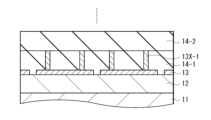
- FIG. 1 is a schematic cross-sectional view showing the configuration of a liquid crystal display element according to an embodiment of the present disclosure.
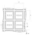
- 2 is a schematic plan view illustrating the structure of a plurality of pixel electrodes of the liquid crystal display element shown in FIG. 1.
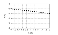
- FIG. FIG. 6 is a characteristic diagram showing the relationship between the width of the upright portion and the reflectance on the drive board side.
- FIG. 2 is a schematic diagram illustrating an example of a method for removing unnecessary diffracted light.
- FIG. 7 is a diagram illustrating another example (correction system) of a method for removing unnecessary diffracted light.
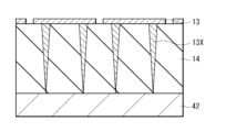
- 2 is a schematic diagram showing an example of a method for manufacturing the liquid crystal display element shown in FIG. 1.
- FIG. FIG. 6A is a schematic diagram showing a process subsequent to FIG.
- FIG. 6A is a schematic cross-sectional view showing an example of the configuration of a general liquid crystal display element.
- FIG. 3 is a schematic cross-sectional view showing another example of the configuration of a general liquid crystal display element.
- 9 is a simulation diagram showing the relationship between the amount of phase modulation and the applied voltage of the liquid crystal display elements shown in FIGS. 1, 7, and 8.
- FIG. 1 is a schematic cross-sectional view showing an example of the configuration of a general liquid crystal display element.
- FIG. 3 is a schematic cross-sectional view showing another example of the configuration of a general liquid crystal display element.
- 9 is a simulation diagram showing the relationship between the amount of phase modulation and the applied voltage of the liquid crystal display elements shown in FIGS. 1, 7, and 8.
- FIG. 1 is a schematic cross-sectional view showing an example of the configuration of a general liquid crystal display element.
- FIG. 3 is a schematic cross-sectional view showing another example of the configuration of a general liquid crystal display element.
- 9 is a simulation
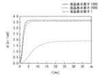
- FIG. 9 is a simulation diagram showing the relationship between the phase modulation amount and time of the liquid crystal display elements shown in FIGS. 1, 7, and 8.
- FIG. FIG. 3 is a schematic cross-sectional view showing an example of the configuration of a liquid crystal display element according to Modification Example 1 of the present disclosure.
- 12 is a schematic plan view showing the structure of a pixel electrode of the liquid crystal display element shown in FIG. 11.
- FIG. FIG. 7 is a schematic cross-sectional view showing an example of the configuration of a liquid crystal display element according to Modification Example 2 of the present disclosure.
- 14 is a schematic plan view showing the structure of a pixel electrode of the liquid crystal display element shown in FIG. 13.
- FIG. 7 is a schematic cross-sectional view showing an example of the configuration of a liquid crystal display element according to Modification Example 3 of the present disclosure.
- 16 is a schematic plan view showing the structure of a pixel electrode of the liquid crystal display element shown in FIG. 15.
- FIG. FIG. 7 is a schematic diagram illustrating a method for manufacturing a liquid crystal display element according to modification example 4 of the present disclosure.
- FIG. 17A is a schematic diagram showing a step following FIG. 17A.
- FIG. 17B is a schematic diagram showing a step following FIG. 17B.
- FIG. 17C is a schematic diagram showing a step following FIG. 17C.
- FIG. 17D is a schematic diagram showing a step following FIG. 17D.
- FIG. 17A is a schematic diagram showing a step following FIG. 17A.
- FIG. 17B is a schematic diagram showing a step following FIG. 17B.
- FIG. 17C is a schematic diagram showing a step following FIG. 17C.
- FIG. 17D is
- FIG. 18A is a schematic diagram showing a step following FIG. 18A.
- FIG. 18B is a schematic diagram showing a step following FIG. 18B.
- FIG. 18C is a schematic diagram showing a step following FIG. 18C.
- FIG. 18D is a schematic diagram showing a step following FIG. 18D.
- FIG. 18E is a schematic diagram showing a step following FIG. 18E. It is a schematic diagram showing the process following FIG. 18F.
- Embodiments of the present disclosure will be described in detail below with reference to the drawings.
- the following description is a specific example of the present disclosure, and the present disclosure is not limited to the following embodiments. Further, the present disclosure is not limited to the arrangement, dimensions, dimensional ratio, etc. of each component shown in each figure.
- the order of explanation is as follows. 1.
- Embodiment (Example of a liquid crystal display element including a pixel electrode having an upright portion facing the liquid crystal layer) 1-1.
- Modification example 2-1 Modification 1 (other example of pixel electrode configuration) 2-2.
- Modification 2 (other example of pixel electrode configuration) 2-3.
- Modification 3 (other example of pixel electrode configuration) 2-4.
- Modification 4 (another example of the method for manufacturing the pixel electrode) 2-5.
- Modification 5 (other example of the method for manufacturing the pixel electrode) 3.
- Application example is
- FIG. 1 shows an example of a schematic cross-sectional configuration of a liquid crystal display element (liquid crystal display element 1) according to an embodiment of the present disclosure.
- the liquid crystal display element 1 is used as a phase modulation element of a display device.
- the liquid crystal display element 1 has a liquid crystal layer 30 between a drive substrate 10 and a counter substrate 20 that are arranged to face each other.
- the drive substrate 10 has a plurality of pixel electrodes 13 provided for each pixel P to which a predetermined voltage is applied by a pixel circuit, and each of the plurality of pixel electrodes 13 has a pixel electrode 13 that is provided vertically facing the liquid crystal layer 30.
- An upright portion 13X is provided.
- the upright portion 13X does not necessarily need to penetrate the reflective film 14.
- the end face of the upright portion 13C may be covered with a portion of the reflective film 14.
- the pixel electrode 13 is made of, for example, aluminum (Al), titanium (Ti), copper (Cu), silicon (Si), silver (Ag), or an alloy thereof (for example, an Al-Cu alloy or an Al-Si alloy). It is made of a metal material that has light reflectivity and is mainly composed of a low resistance metal.
- the upright portion 13X is made of, for example, a conductive material that reflects light in the used wavelength range (for example, visible light). Specific examples include metal materials such as aluminum (Al), copper (Cu), gold (Au), silver (Ag), and tungsten (W).
- the standing portion 13X may be formed using a conductive material having light transmittance, such as indium tin oxide (ITO), indium zinc oxide (IZO), or tin oxide (SnO 2 ). Good too.
- the upright portion 13X can be formed by a process similar to that for the via connecting the pixel circuit and the pixel electrode 13.
- high reflectance can be obtained in a long wavelength region of 500 nm or more.
- the reflection increasing film 14 is for realizing high reflectance of the liquid crystal display element 1.
- the reflection enhancing film 14 is configured using, for example, a dielectric film consisting of one or more layers.
- a dielectric film consisting of multiple layers is a stacked layer in which films made of a low refractive index material (low refractive index film) and films made of a high refractive index material (high refractive index film) are alternately laminated. It is a film, and by controlling the phase of the reflectance occurring at each interface by the film thickness (optical path length), it is theoretically possible to achieve a reflectance close to 100%.
- Examples of materials constituting the low refractive index film include silicon oxide (SiO 2 ) and magnesium fluoride (MgF 2 ).
- Examples of materials constituting the high refractive index film include titanium oxide (TiO 2 ), tantalum oxide (TaO 2 ), aluminum oxide (Al 2 O 3 ), zirconium oxide (ZrO 2 ), and hafnium oxide (HfO 2 ). can be mentioned.
- the thickness of the reflection-enhancing film 14 depends on the desired reflectance, the length of the target wavelength whose reflectance is to be amplified, and the refractive index of the reflective film. For example, when eight pairs of low refractive index films and high refractive index films are laminated to achieve a reflectance of nearly 100% at a wavelength of 1064 nm, the total film thickness may be about 3 ⁇ m.
- an enhanced reflection film 14 that has high light resistance and heat resistance to light in the wavelength range used (for example, visible light).
- This makes it possible to realize a liquid crystal display element 1 compatible with high-power lasers.
- a liquid crystal display element 1 that can withstand pulsed lasers such as femtosecond lasers, which have a small average output but a very large instantaneous light intensity. Thereby, it can be used for microfabrication applications such as two-photon absorption 3D printers.
- the alignment film 15 controls the alignment of the liquid crystal layer 30, and is made of an inorganic material such as silicon oxide (SiO 2 ), diamond-like carbon, or aluminum oxide (Al 2 O 3 ). In addition, it may be made of an organic material such as polyimide (PI) or polyimide (PVA).
- PI polyimide
- PVA polyimide
- the thickness of the alignment film 15 is, for example, 50 nm or more and 500 nm or less.
- the alignment film 15 can be formed using, for example, a vapor deposition method, a rubbing method, or a photoalignment method.
- the counter substrate 20 includes, for example, a light-transmitting substrate 21, a counter electrode 22, and an alignment film 23.
- the counter electrode 22 and the alignment film 23 are provided in this order on the surface of the substrate 21 on the liquid crystal layer 30 side.
- the alignment film 23 controls the alignment of the liquid crystal layer 30, and is made of an inorganic material such as silicon oxide (SiO 2 ), diamond-like carbon, or aluminum oxide (Al 2 O 3 ). In addition, it may be made of an organic material such as polyimide (PI) or polyimide (PVA).
- the thickness of the alignment film 23 is, for example, 50 nm or more and 500 nm or less.
- the alignment film 15 can be formed using, for example, a vapor deposition method, a rubbing method, or a photoalignment method.
- FIG. 5 shows another example (correction system 5) of the method for removing unnecessary diffracted light.
- the display device including the liquid crystal display element 1 may be provided with a correction processing function (correction system 5) that corrects the spatial phase distribution caused by providing the upright portion 13X.
- the correction system 5 is formed during the iteration of performing light propagation calculations such as the angular spectrum method and the GS (Gerchgerg-Saxton) method to derive the CGH (Computer Generated Hologram) pattern to be displayed.
- This can be realized by incorporating the spatial phase distribution specific to the structure of the upright portion 13X. In this way, by correcting the spatial phase distribution specific to the structure of the upright portion 13X through signal processing, it is possible to approximate the ideal phase distribution. Therefore, unnecessary diffracted light is reduced and light utilization efficiency is increased.
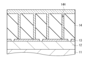
- an opening 14H that penetrates the reflection-enhancing film 14 to the pixel electrode 13 is formed by dry processing.
- a conductive film is embedded in the opening 14H using, for example, a CVD method or an atomic layer deposition (ALD) method.
- a passivation film may be formed after forming the upright portion 13X. This improves the flatness of the surface of the reflective film 14.
- the drive substrate 10 and the counter substrate 20 are bonded together with a gap left between them, and then liquid crystal is injected between the drive substrate 10 and the counter substrate 20 to form a liquid crystal layer 30.
- the liquid crystal display element 1 shown in FIG. 1 is completed.
- the liquid crystal display element 1 of the present embodiment has a pixel electrode 13 provided for each pixel P, to which a predetermined voltage is applied by a pixel circuit that drives the liquid crystal layer 30 for each pixel P, toward the liquid crystal layer 30.
- An upright portion 13X having, for example, a partition wall structure is provided. This increases the effective potential applied to the liquid crystal layer 30. This will be explained below.
- SLMs Spatial light modulators
- DMD Digital Mirror Device
- MRAM Magnetic Random Access Memory
- LCOS Liquid Crystal on Silicon
- the optical phase of the light is controlled by applying a voltage to a liquid crystal layer made of a liquid crystal material having optical anisotropy and dielectric anisotropy to change the optical path length of each pixel perceived by the incident light.
- a liquid crystal layer made of a liquid crystal material having optical anisotropy and dielectric anisotropy to change the optical path length of each pixel perceived by the incident light.
- the liquid crystal molecules of the pixel to which a voltage is applied are generally aligned in the horizontal direction of the substrate, while the liquid crystal molecules in the pixel to which a voltage is applied are generally aligned in the horizontal direction of the substrate.
- liquid crystal molecules are oriented in a direction perpendicular to the substrate, so the optical path length becomes large in the pixel to which a voltage is applied. As a result, an arbitrary spatial phase distribution is created, and the function of condensing and deflecting light is realized.
- Dielectric multilayer films are generally used to achieve high reflectance in reflective LCOS.
- a dielectric multilayer film is a laminated film in which low refractive index films and high refractive index films are alternately laminated, and the phase of reflectance occurring at each interface is controlled by the film thickness (optical path length). By doing so, it is possible to theoretically achieve a reflectance close to 100%. It is actually used in commercially available LCOS-SLMs, and although it depends on the aperture ratio, there are also elements that achieve a reflectance of over 95%.
- the dielectric multilayer film plays an important role in improving light resistance against high-power lasers.
- Aluminum (Al) which is generally used in reflective LCOS, exhibits absorption of nearly 10% in the visible light region as described above.
- dielectric multilayer films are widely used in high-output mirrors and the like, which suppress element absorption and improve reflectance.
- each of the plurality of pixel electrodes 13 provided for each pixel P is provided with an upright portion 13X having a partition wall structure and standing upright toward the liquid crystal layer 30.
- FIG. 7 shows an example of a schematic cross-sectional configuration of a general liquid crystal display element 1000 having an insulating film 1014 for flattening the surface between a plurality of pixel electrodes 1013 and an alignment film 1015.
- the liquid crystal display element 1000 includes a driving substrate 1010 in which a pixel circuit layer 1012, a plurality of pixel electrodes 1013, an insulating film 1014, and an alignment film 1015 are laminated in this order on a substrate 1011, and a counter electrode on one surface of a substrate 1021.
- a liquid crystal layer 1030 is provided between the liquid crystal layer 1022 and a counter substrate 1020 provided with an alignment film 1023.
- FIG. 8 shows an example of a schematic cross-sectional configuration of a general liquid crystal display element 2000 having a reflection increasing film 2014 made of a dielectric multilayer film between a plurality of pixel electrodes 2013 and an alignment film 2015.
- the liquid crystal display element 2000 includes a driving substrate 2010 in which a pixel circuit layer 2012, a plurality of pixel electrodes 2013 without an upright portion, a reflection increasing film 2014, and an alignment film 2015 are laminated in this order on a substrate 2011, and a substrate 2021.
- a liquid crystal layer 2030 is provided between a counter substrate 2020 on one surface of which a counter electrode 2022 and an alignment film 2023 are provided.
- FIG. 9 shows the results of simulating the relationship between the amount of phase modulation and the applied voltage for the liquid crystal display elements 1, 1000, and 2000 shown in FIGS. 1, 7, and 8 using a liquid crystal alignment simulator (LCDMaster).
- FIG. 10 shows the results of simulating the relationship between the phase modulation amount and time of the liquid crystal display elements 1, 1000, and 2000 shown in FIGS. 1, 7, and 8 using a liquid crystal alignment simulator (LCDMaster).
- Table 1 shows the reflectance (Fig. 3), phase modulation amount (Fig. 9), and response speed (Fig. 10) of the liquid crystal display elements 1, 1000, and 2000 shown in Figs. 1, 7, and 8. The values are summarized as relative values with the value of 1000 as the reference value (1.00).
- the preconditions for numerical calculations were as follows. (Numerical calculation prerequisites) Wavelength: 550nm Standing part width: 0.3 ⁇ m Pixel pitch: 4.2 ⁇ m Response speed: Phase modulation amount 10% to 90%
- the liquid crystal display element 1 having the upright portion 13X penetrating the reflection-enhancing film 14 is equivalent to the liquid crystal display element 2000 having no upright portion and having the reflection-enhancing film 2014 made of a dielectric multilayer film. It was confirmed that it exhibited reflectance. Regarding the amount of phase modulation, it was confirmed that the liquid crystal display element 1 having the upright portion 13X penetrating the reflection enhancing film 14 exhibited the same maximum amount of phase modulation as the liquid crystal display element 1000 without a dielectric film. Regarding the response speed, it was confirmed that the liquid crystal display element 1 having the upright portion 13X penetrating the reflection enhancing film 14 exhibited a response speed equivalent to that of the liquid crystal display element 1000 without a dielectric film.
- liquid crystal display element 1 of this embodiment it is possible to amplify the amount of phase modulation and improve the response speed while improving the reflectance.
- FIG. 11 shows an example of a schematic cross-sectional configuration of a liquid crystal display element (liquid crystal display element 1A) according to Modification Example 1 of the present disclosure.
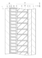
- FIG. 12 schematically represents an example of the planar configuration of the plurality of pixel electrodes 13 of the liquid crystal display element 1A shown in FIG. 11, and FIG. 11 corresponds to the II-II line shown in FIG. It represents a cross section.
- the liquid crystal display element 1A includes a partition structure continuously formed along the outer shape of the pixel electrode 13 as an upright portion 13X that stands upright toward the liquid crystal layer 30 provided on each of the plurality of pixel electrodes 13, and a partition structure inside the partition wall structure.
- This embodiment differs from the above embodiment in that it has a columnar structure provided in the above embodiment.
- the flatness of the electric field distribution applied to the liquid crystal layer 30 is improved compared to the liquid crystal display element 1 of the above embodiment. This reduces unnecessary diffracted light caused by the spatial distribution of rotation angles of liquid crystal molecules. Therefore, in addition to the effects of the embodiments described above, it is possible to improve light utilization efficiency.
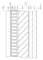
- the liquid crystal display element 1B includes a partition structure continuously formed along the outer shape of the pixel electrode 13 as an upright portion 13X that stands toward the liquid crystal layer 30 provided on each of the plurality of pixel electrodes 13, and a partition structure inside the partition wall structure.
- a plurality of (three in this case) columnar structures are provided.
- the flatness of the electric field distribution applied to the liquid crystal layer 30 is further improved compared to the liquid crystal display element 1A of the modification 1, and the rotation angle of the liquid crystal molecules is improved. Unnecessary diffracted light due to spatial distribution is further reduced. Therefore, in addition to the effects of the embodiments described above, it is possible to further improve light utilization efficiency.
- FIG. 15 shows an example of a schematic cross-sectional configuration of a liquid crystal display element (liquid crystal display element 1C) according to modification example 3 of the present disclosure.
- FIG. 16 schematically represents an example of the planar configuration of the plurality of pixel electrodes 13 of the liquid crystal display element 1C shown in FIG. 15, and FIG. 15 corresponds to the IV-IV line shown in FIG. It represents a cross section.
- Modifications 1 and 2 above an example was shown in which one or more columnar structures were provided inside the partition structure as the upright portions 13X, but the present invention is not limited to this.
- the liquid crystal display element 1C includes a multiple partition wall structure continuously formed along the outer shape of the pixel electrode 13 as a standing portion 13X that stands upright toward the liquid crystal layer 30 provided on each of the plurality of pixel electrodes 13. This embodiment differs from the above embodiment in this respect.
- the flatness of the electric field distribution applied to the liquid crystal layer 30 is further improved compared to the liquid crystal display elements 1A and 1B of the modification 1, and the rotation of the liquid crystal molecules is improved. Unnecessary diffracted light due to the spatial distribution of corners is further reduced. Therefore, in addition to the effects of the embodiments described above, it is possible to further improve light utilization efficiency.
- (2-4. Modification example 4) 17A to 17E schematically represent an example of a method for manufacturing the pixel electrode 13 of the liquid crystal display element 1 according to Modification 4 of the present disclosure.
- the pixel electrode 13 of the liquid crystal display element 1 of the above embodiment can be formed using the following method.
- a plurality of pixel electrodes 13 are formed on the pixel circuit layer 12 for each pixel P in the same manner as in the above embodiment, and then, as a part of the reflection increasing film 14, for example, the pixel electrodes 13 are formed by vapor deposition.
- a dielectric multilayer film 14-1 is formed by alternately forming a low refractive index film and a high refractive index film using the method.
- FIG. 17B after patterning a resist film 41 on the dielectric multilayer film 14-1 using lithography technology, dry processing is performed to form an opening that penetrates the dielectric multilayer film 14-1 to the pixel electrode 13. 14H is formed.
- a standing portion 13X is formed in each of the plurality of pixel electrodes 13, standing toward the liquid crystal layer 30 and penetrating the reflection increasing film 14.
- an alignment film 15 is formed on the reflection increasing film 14 using, for example, a CVD method.
- a reflection enhancing film 14 made of a dielectric multilayer film is formed by alternately forming a low refractive index film and a high refractive index film on the support substrate 42 using, for example, a vapor deposition method. do.
- a resist film 41 is patterned on the reflection-enhancing film 14 by lithography
- an opening 14H passing through the reflection-enhancing film 14 to the support substrate 42 is formed by dry processing.
- the pixel circuit layer 12 including the pad portion 43 is formed.
- the support substrate 42 is reversed to form a pad portion 43 exposed on the surface of the pixel circuit layer 12, and a pad portion 43 exposed on the surface of the pixel circuit layer 12 provided on the separately formed substrate 11.
- the portion 44 is pasted together.
- the support substrate 42 is removed.
- the conductive material is a metal that reflects visible light.
- the one or more standing portions are formed using aluminum (Al), copper (Cu), gold (Au), silver (Ag), or tungsten (W).
- the conductive material has optical transparency.
- the one or more standing portions are formed using indium tin oxide (ITO), indium zinc oxide (IZO), or tin oxide (SnO 2 ).
- the liquid crystal display device according to any one of ).
- (12) The liquid crystal display element according to any one of (5) to (11), wherein each of the first substrate and the second substrate further has an alignment film on a surface facing the liquid crystal layer.
- (12) The liquid crystal display element according to (12), wherein the alignment film provided on the first substrate is provided on the dielectric film made of one or more layers.
- the second substrate further includes a second electrode common to the plurality of pixels, The liquid crystal display element according to (12) or (13), wherein the alignment film provided on the second substrate is provided on the second electrode.
- the liquid crystal display element is a liquid crystal layer; a first substrate having a pixel circuit that drives the liquid crystal layer for each pixel; a second substrate disposed opposite to the first substrate with the liquid crystal layer in between; and a plurality of first electrodes provided on the first substrate for each pixel and having one or more standing portions standing upright toward the liquid crystal layer, to which a predetermined voltage is applied by the pixel circuit.
- Display device (16) The display device according to (15) above, further comprising a correction system that flattens the phase difference distribution in the display area.
Landscapes
- Physics & Mathematics (AREA)
- Nonlinear Science (AREA)
- Mathematical Physics (AREA)
- Chemical & Material Sciences (AREA)
- Crystallography & Structural Chemistry (AREA)
- General Physics & Mathematics (AREA)
- Optics & Photonics (AREA)
- Liquid Crystal (AREA)
Priority Applications (2)
| Application Number | Priority Date | Filing Date | Title |
|---|---|---|---|
| JP2024528723A JPWO2023243460A1 (https=) | 2022-06-15 | 2023-06-05 | |
| CN202380045695.2A CN119325572A (zh) | 2022-06-15 | 2023-06-05 | 液晶显示元件及显示装置 |
Applications Claiming Priority (2)
| Application Number | Priority Date | Filing Date | Title |
|---|---|---|---|
| JP2022-096656 | 2022-06-15 | ||
| JP2022096656 | 2022-06-15 |
Publications (1)
| Publication Number | Publication Date |
|---|---|
| WO2023243460A1 true WO2023243460A1 (ja) | 2023-12-21 |
Family
ID=89191127
Family Applications (1)
| Application Number | Title | Priority Date | Filing Date |
|---|---|---|---|
| PCT/JP2023/020813 Ceased WO2023243460A1 (ja) | 2022-06-15 | 2023-06-05 | 液晶表示素子および表示装置 |
Country Status (3)
| Country | Link |
|---|---|
| JP (1) | JPWO2023243460A1 (https=) |
| CN (1) | CN119325572A (https=) |
| WO (1) | WO2023243460A1 (https=) |
Citations (4)
| Publication number | Priority date | Publication date | Assignee | Title |
|---|---|---|---|---|
| JPH1020284A (ja) * | 1996-07-03 | 1998-01-23 | Matsushita Electric Ind Co Ltd | 液晶表示パネル |
| JP2002214613A (ja) * | 2001-01-16 | 2002-07-31 | Mitsubishi Electric Corp | 液晶表示装置 |
| JP2004318077A (ja) * | 2003-03-18 | 2004-11-11 | Fujitsu Display Technologies Corp | 液晶表示装置及びその製造方法 |
| JP2007133371A (ja) * | 2005-10-14 | 2007-05-31 | Semiconductor Energy Lab Co Ltd | 表示装置及びその作製方法 |
-
2023
- 2023-06-05 CN CN202380045695.2A patent/CN119325572A/zh active Pending
- 2023-06-05 WO PCT/JP2023/020813 patent/WO2023243460A1/ja not_active Ceased
- 2023-06-05 JP JP2024528723A patent/JPWO2023243460A1/ja active Pending
Patent Citations (4)
| Publication number | Priority date | Publication date | Assignee | Title |
|---|---|---|---|---|
| JPH1020284A (ja) * | 1996-07-03 | 1998-01-23 | Matsushita Electric Ind Co Ltd | 液晶表示パネル |
| JP2002214613A (ja) * | 2001-01-16 | 2002-07-31 | Mitsubishi Electric Corp | 液晶表示装置 |
| JP2004318077A (ja) * | 2003-03-18 | 2004-11-11 | Fujitsu Display Technologies Corp | 液晶表示装置及びその製造方法 |
| JP2007133371A (ja) * | 2005-10-14 | 2007-05-31 | Semiconductor Energy Lab Co Ltd | 表示装置及びその作製方法 |
Also Published As
| Publication number | Publication date |
|---|---|
| CN119325572A (zh) | 2025-01-17 |
| JPWO2023243460A1 (https=) | 2023-12-21 |
Similar Documents
| Publication | Publication Date | Title |
|---|---|---|
| JP6285662B2 (ja) | 可変光学リターダ | |
| US20230030594A1 (en) | Systems and Methods for Fabricating a Multilayer Optical Structure | |
| JP7612592B2 (ja) | 統合された格子を使用してホログラフィック導波管ディスプレイを提供するための方法および装置 | |
| JP4084203B2 (ja) | 光偏向装置 | |
| CN115917367A (zh) | 基于纳米颗粒的全息光聚合物材料和相关应用 | |
| US6295145B1 (en) | Switchable holographic device | |
| JP5270142B2 (ja) | 反射型空間光変調素子 | |
| CN113820895A (zh) | 一种基于超构表面的像素化动态全息显示器件及实现方法 | |
| TWI906722B (zh) | 超透鏡陣列及具有該超透鏡陣列的顯示裝置 | |
| WO2016080385A1 (ja) | 液晶表示装置 | |
| JP2006126551A (ja) | 液晶表示装置 | |
| JP2001330844A5 (https=) | ||
| JP4717087B2 (ja) | 光偏向装置 | |
| JPWO2017086116A1 (ja) | 半導体装置および投射型表示装置 | |
| WO2023243460A1 (ja) | 液晶表示素子および表示装置 | |
| WO2017173688A1 (zh) | 3d显示装置 | |
| JP2008250220A (ja) | 反射型光変調装置 | |
| US12044921B2 (en) | Spatial light modulator and method of forming the same | |
| JP2010122704A5 (https=) | ||
| JP7574300B2 (ja) | 光学装置 | |
| US12386224B1 (en) | Cholesteric liquid crystal polarizing grating | |
| JPH0318829A (ja) | 空間光変調素子 | |
| JPH0566393A (ja) | 液晶素子及び液晶表示装置 | |
| CN1728016A (zh) | 一种电子全息显示器件 | |
| WO2025088944A1 (ja) | 液晶素子および位相変調装置 |
Legal Events
| Date | Code | Title | Description |
|---|---|---|---|
| 121 | Ep: the epo has been informed by wipo that ep was designated in this application |
Ref document number: 23823753 Country of ref document: EP Kind code of ref document: A1 |
|
| WWE | Wipo information: entry into national phase |
Ref document number: 2024528723 Country of ref document: JP |
|
| WWE | Wipo information: entry into national phase |
Ref document number: 202380045695.2 Country of ref document: CN |
|
| NENP | Non-entry into the national phase |
Ref country code: DE |
|
| WWP | Wipo information: published in national office |
Ref document number: 202380045695.2 Country of ref document: CN |
|
| 122 | Ep: pct application non-entry in european phase |
Ref document number: 23823753 Country of ref document: EP Kind code of ref document: A1 |