WO2023243169A1 - 電力変換装置 - Google Patents
電力変換装置 Download PDFInfo
- Publication number
- WO2023243169A1 WO2023243169A1 PCT/JP2023/010455 JP2023010455W WO2023243169A1 WO 2023243169 A1 WO2023243169 A1 WO 2023243169A1 JP 2023010455 W JP2023010455 W JP 2023010455W WO 2023243169 A1 WO2023243169 A1 WO 2023243169A1
- Authority
- WO
- WIPO (PCT)
- Prior art keywords
- wiring
- interphase
- positive electrode
- negative electrode
- laminated
- Prior art date
- Legal status (The legal status is an assumption and is not a legal conclusion. Google has not performed a legal analysis and makes no representation as to the accuracy of the status listed.)
- Ceased
Links
Images


Classifications
-
- H—ELECTRICITY
- H02—GENERATION; CONVERSION OR DISTRIBUTION OF ELECTRIC POWER
- H02M—APPARATUS FOR CONVERSION BETWEEN AC AND AC, BETWEEN AC AND DC, OR BETWEEN DC AND DC, AND FOR USE WITH MAINS OR SIMILAR POWER SUPPLY SYSTEMS; CONVERSION OF DC OR AC INPUT POWER INTO SURGE OUTPUT POWER; CONTROL OR REGULATION THEREOF
- H02M7/00—Conversion of AC power input into DC power output; Conversion of DC power input into AC power output
- H02M7/003—Constructional details, e.g. physical layout, assembly, wiring or busbar connections
-
- H—ELECTRICITY
- H10—SEMICONDUCTOR DEVICES; ELECTRIC SOLID-STATE DEVICES NOT OTHERWISE PROVIDED FOR
- H10W—GENERIC PACKAGES, INTERCONNECTIONS, CONNECTORS OR OTHER CONSTRUCTIONAL DETAILS OF DEVICES COVERED BY CLASS H10
- H10W70/00—Package substrates; Interposers; Redistribution layers [RDL]
- H10W70/60—Insulating or insulated package substrates; Interposers; Redistribution layers
- H10W70/611—Insulating or insulated package substrates; Interposers; Redistribution layers for connecting multiple chips together
-
- H—ELECTRICITY
- H10—SEMICONDUCTOR DEVICES; ELECTRIC SOLID-STATE DEVICES NOT OTHERWISE PROVIDED FOR
- H10D—INORGANIC ELECTRIC SEMICONDUCTOR DEVICES
- H10D80/00—Assemblies of multiple devices comprising at least one device covered by this subclass
- H10D80/30—Assemblies of multiple devices comprising at least one device covered by this subclass the at least one device being covered by groups H10D84/00 - H10D86/00, e.g. assemblies comprising integrated circuit processor chips
-
- H—ELECTRICITY
- H10—SEMICONDUCTOR DEVICES; ELECTRIC SOLID-STATE DEVICES NOT OTHERWISE PROVIDED FOR
- H10W—GENERIC PACKAGES, INTERCONNECTIONS, CONNECTORS OR OTHER CONSTRUCTIONAL DETAILS OF DEVICES COVERED BY CLASS H10
- H10W70/00—Package substrates; Interposers; Redistribution layers [RDL]
- H10W70/60—Insulating or insulated package substrates; Interposers; Redistribution layers
- H10W70/62—Insulating or insulated package substrates; Interposers; Redistribution layers characterised by their interconnections
- H10W70/65—Shapes or dispositions of interconnections
-
- H—ELECTRICITY
- H10—SEMICONDUCTOR DEVICES; ELECTRIC SOLID-STATE DEVICES NOT OTHERWISE PROVIDED FOR
- H10W—GENERIC PACKAGES, INTERCONNECTIONS, CONNECTORS OR OTHER CONSTRUCTIONAL DETAILS OF DEVICES COVERED BY CLASS H10
- H10W70/00—Package substrates; Interposers; Redistribution layers [RDL]
- H10W70/60—Insulating or insulated package substrates; Interposers; Redistribution layers
- H10W70/67—Insulating or insulated package substrates; Interposers; Redistribution layers characterised by their insulating layers or insulating parts
- H10W70/68—Shapes or dispositions thereof
- H10W70/685—Shapes or dispositions thereof comprising multiple insulating layers
-
- H—ELECTRICITY
- H10—SEMICONDUCTOR DEVICES; ELECTRIC SOLID-STATE DEVICES NOT OTHERWISE PROVIDED FOR
- H10W—GENERIC PACKAGES, INTERCONNECTIONS, CONNECTORS OR OTHER CONSTRUCTIONAL DETAILS OF DEVICES COVERED BY CLASS H10
- H10W90/00—Package configurations
-
- H—ELECTRICITY
- H10—SEMICONDUCTOR DEVICES; ELECTRIC SOLID-STATE DEVICES NOT OTHERWISE PROVIDED FOR
- H10D—INORGANIC ELECTRIC SEMICONDUCTOR DEVICES
- H10D1/00—Resistors, capacitors or inductors
- H10D1/60—Capacitors
- H10D1/68—Capacitors having no potential barriers
-
- H—ELECTRICITY
- H10—SEMICONDUCTOR DEVICES; ELECTRIC SOLID-STATE DEVICES NOT OTHERWISE PROVIDED FOR
- H10W—GENERIC PACKAGES, INTERCONNECTIONS, CONNECTORS OR OTHER CONSTRUCTIONAL DETAILS OF DEVICES COVERED BY CLASS H10
- H10W40/00—Arrangements for thermal protection or thermal control
- H10W40/20—Arrangements for cooling
- H10W40/25—Arrangements for cooling characterised by their materials
- H10W40/258—Metallic materials
Definitions
- the present invention relates to a power conversion device.
- the main circuit of inverters used in automobiles is constructed using a printed circuit board for conducting current, and as a result, there is a need to improve productivity and reduce inductance while meeting the performance of hybrid and electric vehicles. It is necessary to respond to
- Patent Document 1 discloses a configuration in which a positive electrode wiring and a negative electrode conductor connecting each power module and each capacitor are laminated to realize a reduction in inductance.
- Patent Document 1 the positive electrode wiring and the negative electrode wiring are stacked in all areas, and each wiring is mixed.
- each wiring is separated.
- a problem arises in that electrical resistance increases. This makes it difficult to reduce the wiring temperature and requires improvement in cooling performance.
- the power conversion device includes a plurality of circuit bodies each having a plurality of power semiconductor elements, and a wiring board electrically connected to the circuit bodies and provided with a plurality of positive electrode wirings and negative electrode wirings laminated in the thickness direction. , a plurality of smoothing capacitors provided corresponding to the plurality of circuit bodies, respectively, and the wiring board includes a plurality of laminated wiring portions to which the plurality of circuit bodies and the plurality of smoothing capacitors are connected, respectively; interphase wiring parts formed between the plurality of laminated wiring parts, in the laminated wiring part, the positive electrode wiring and the negative electrode wiring are stacked on top of each other, and in the interphase wiring part, the plurality of the The positive electrode wiring and the plurality of negative electrode wirings are separately stacked on a plane of the wiring board, and the interphase wiring portion has a via penetrating the wiring board in a thickness direction.
- the present invention it is possible to provide a power converter device that achieves both high current and low inductance of the substrate while improving heat dissipation.
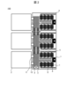
- the plurality of circuit bodies 1 constituting the power conversion circuit are each composed of semiconductor elements such as IGBTs (Insulated Gate Bipolar Transistors) and MOSFETs (Metal-Oxide-Semiconductor Field-Effect Transistors).
- IGBTs Insulated Gate Bipolar Transistors
- MOSFETs Metal-Oxide-Semiconductor Field-Effect Transistors
- Two series-connected circuit bodies 1 and one capacitor 2 form a pair, each forming a circuit for one phase, forming a three-phase power conversion circuit.
- Each circuit is connected to a positive electrode wiring 3 and a negative electrode wiring 4.
- the circuit body 1 has a high voltage side terminal for the main circuit (a collector terminal for an IGBT, a drain terminal for a MOSFET) and a low voltage side terminal for the main circuit (an emitter terminal for an IGBT, a source terminal for a MOSFET). , and a control terminal (gate terminal).
- the power conversion device 100 includes a plurality of circuit bodies 1 each having a plurality of power semiconductor elements, and a plurality of positive electrode wirings 3 and negative electrode wirings 4 which are electrically connected to the circuit bodies 1 and are laminated in the thickness direction.
- the circuit board 6 includes a wiring board 6 (hereinafter referred to as a board 6), and a plurality of smoothing capacitors 2 provided corresponding to the plurality of circuit bodies 1, respectively.
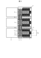
- the positive electrode wiring 3 and the negative electrode wiring 4 are stacked on each other in the thickness direction of the substrate 6 (from the front to the back of the paper in FIG. 2), and connect the capacitors 2 of each phase to the circuit body 1 (see FIGS. 4 to 4 for details). (described later in Section 8). Note that FIG.
- circuit body 1 shows a configuration example in which four circuit bodies 1 are arranged in parallel, eight circuit bodies 1 are used as a one-phase circuit, and three phases are provided on the board 6. In this way, the circuit body 1 may be arranged in multiple parallel connections depending on the desired output current value.
- the substrate 6 has a plurality of conductor layers in the thickness direction, and each conductor layer is laminated with a resin layer interposed therebetween.
- a positive electrode wiring 3, a negative electrode wiring 4, an output wiring 7, and a signal wiring 9 are formed on the conductor layer of the substrate 6.
- the circuit body 1 and the capacitor 2 are connected to the positive electrode wiring 3 and the negative electrode wiring 4 using a bonding material such as solder.
- the circuit body 1 has a signal terminal 8 for connection to a signal wiring 9.
- the positive electrode wiring 3, the negative electrode wiring 4, and the output wiring 7 are each formed to be thicker than the signal wiring 9 connected to the circuit body 1, and the current to be supplied to the load to which they are connected is larger than that of other wirings. This corresponds to the fact that it is an electric current.
- the positive electrode wiring 3 and the negative electrode wiring 4 have through-vias 5 (hereinafter referred to as vias 5).
- the via 5 is provided in a region where the positive electrode wiring 3 and the negative electrode wiring 4 of each phase are not stacked on each other.
- vias 5 are formed by penetrating the substrate 6 in the thickness direction, so that the wirings having the same potential are electrically connected to each other.
- the positive electrode wiring 3 is connected to the positive terminal of a DC voltage source such as a battery (not shown), and the negative electrode wiring 4 is connected to the negative terminal of a DC voltage source such as a battery (not shown).
- a DC voltage source such as a battery (not shown)
- the negative electrode wiring 4 is connected to the negative terminal of a DC voltage source such as a battery (not shown).
- the capacitors 2 are connected in line along the substrate 6 in order to satisfy the capacitance determined according to the desired amount of input voltage fluctuation. It has a positive terminal 10 and a negative terminal 11 as terminals.
- the positive electrode terminal 10 of the capacitor 2 is electrically connected to the main circuit high voltage side terminal of the circuit body 1 on the high side (upper arm) side by being connected to the positive electrode wiring 3. Further, the positive electrode wiring 3 is connected to the positive electrode terminal 10 of the capacitor 2 of the other phase and the high voltage side terminal for the main circuit of the circuit body 1 on the high side side of the other phase.
- the negative electrode terminal 11 of the capacitor 2 is connected to the negative electrode wiring 4 and thereby connected to the main circuit low voltage side terminal of the circuit body 1 on the low side (lower arm) side.
- the negative electrode wiring 4 is connected to the negative electrode terminal 11 of the capacitor 2 of the other phase and the main circuit low voltage side terminal 12 of the low side circuit body 1 of the other phase.
- the main circuit low voltage side terminal of the circuit body 1 on the high side side is connected to the main circuit high voltage side terminal of the circuit body 1 on the low side side by the output wiring 7 of each phase.
- the output wiring 7 of each phase is connected to a load such as a motor (not shown).
- the control terminal of the circuit body 1 is connected to a control circuit (not shown), and is turned on or off based on a signal input from a higher-level control device such as a microcomputer, thereby outputting an alternating current voltage to a load such as a motor. do.
- a control circuit not shown
- the substrate 6 includes a plurality of laminated wiring sections 15 to which the plurality of circuit bodies 1 and a plurality of smoothing capacitors 2 are respectively connected, and interphase wiring sections 16 formed between the plurality of laminated wiring sections 15.
- the positive electrode wires 3 and the negative electrode wires 4 are stacked on top of each other, but in the interphase wiring section 16, the plurality of positive electrode wires 3 and the plurality of negative electrode wires 4 are separated on the plane of the substrate 6, respectively. And they are wired in parallel and stacked. That is, the interphase wiring portion 16 is a region where the positive electrode wiring 3 and the negative electrode wiring 4 are not stacked on each other in the thickness direction of the substrate 6.
- the interphase wiring section 16 has a via 5 that penetrates the substrate 6 in the thickness direction, but the laminated wiring section 15 does not have a via 5.
- the interphase wiring section 16 has vias 5 to improve heat dissipation.
- the laminated wiring section 15 does not have the via 5, it has a structure in which the positive electrode wiring 3 and the negative electrode wiring 4 are not separated by the through via 5, so that the wiring of the positive electrode wiring 3 and the negative electrode wiring 4 is This suppresses the reduction in cross-sectional area and reduces inductance.
- the plurality of circuit bodies 1 have main circuit terminals 12 on the substrate 6.
- This main circuit terminal 12 is arranged within a region 12a perpendicular to one side defined by the distance between the positive terminal 10 and the negative terminal 11 of the smoothing capacitor 2.
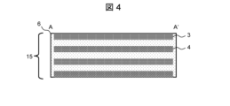
- the laminated wiring section 15 As shown in FIG. 4, in the laminated wiring section 15, for example, when the substrate 6 has four conductor layers, the first and third layers from the top surface of the substrate 6 are the positive electrode wiring 3, and the second and fourth layers are the positive electrode wiring 3. This becomes the negative electrode wiring 4.
- the laminated wiring portion 15 is a region where the positive electrode wiring 3 and the negative electrode wiring 4 are stacked and overlapped with each other.
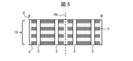
- the interphase wiring section 16 is a region provided between the laminated wiring sections 15, and the positive electrode wiring 3 and the negative electrode wiring 4 are stacked with each other without overlapping each other. There is.
- the interphase wiring section 16 electrically connects the positive electrode wiring 3 and the negative electrode wiring 4, which have the same potential, to each other from the top to the bottom of the substrate 6 through the vias 5 provided in the thickness direction of the substrate 6. are doing.
- Two or more vias 5 of the interphase wiring section 16 are provided in each of the positive electrode wiring 3 and the negative electrode wiring 4. Further, in the interphase wiring section 16, the via 5 is located at a position closer to the laminated wiring section 15 adjacent to the interphase wiring section 16 than the center line 6a perpendicular to the arrangement direction of the laminated wiring section 15 and the interphase wiring section 16. Each is provided. Thereby, even if only a small number of vias 5 are provided, the wiring temperature of the substrate 6 can be efficiently reduced. In addition, for the laminated wiring part 15 where the via 5 is not provided and it is difficult to cool the wiring, by arranging the via 5 near the laminated wiring part 15 in the interphase wiring part 16, the laminated wiring part 15 can be cooled. Reduces wiring temperature.
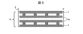
- each wiring can be laminated using blind vias 5a.
- the first and second layers from the top surface of the substrate 6 are used as positive electrode wiring 3
- the third and fourth layers are used as negative electrode wiring 4
- the wirings of the same potential are connected by blind vias 5a.
- the positive electrode wiring 3 and the negative electrode wiring 4 can be stacked, respectively, without reducing the cross-sectional area of the positive electrode wiring 3 and the negative electrode wiring 4.
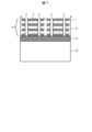
- FIG. 7 A cooler 14 that cools the plurality of circuit bodies 1 is arranged on one surface of the board 6 .
- An insulating heat radiating member 13 is provided between the cooler 14 and the substrate 6. Since the heat dissipation member 13 is a member that improves adhesion by following the steps and warpage of the substrate 6, a low-hardness resin or the like is used. Furthermore, the cooler 14 is constructed of a material with high thermal conductivity such as aluminum. As a result, heat generated when current is passed through the positive electrode wiring 3 and the negative electrode wiring 4 is radiated from the substrate 6 to the cooler 14 via the heat dissipation member 13 via the via 5 of the interphase wiring section 16. The wiring temperature of the board 6 can be reduced.
- the via 5 must be provided on the substrate 6 where the positive electrode wiring 3 and the negative electrode wiring 4 are mixed in the past, so that the positive electrode wiring 3 and the negative electrode wiring 4 are separated by the amount of the via 5. Resolved the increasing number of issues.
- the positive electrode wiring 3 and the negative electrode wiring 4 are arranged in parallel, so that the current flowing through the positive electrode wiring 3 and the current flowing through the negative electrode wiring 4 are opposite to each other on the left and right sides. Therefore, the magnetic field is canceled and the inductance is reduced. Furthermore, the resonance current generated between the capacitors 2 (see FIGS.
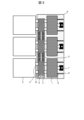
- FIG. 9 shows a configuration example in which the high-side circuit body 1 and the low-side circuit body 1 are integrated. Thereby, the circuit body 1 can be easily mounted on the board 6, and the wiring inductance of each phase can be reduced and the temperature of the board 6 can be reduced at the same time.
- the inverter of the present invention described above with reference to FIGS. 1 to 9 does not have to be limited to three-phase.
- a wiring board provided with a plurality of circuit bodies 1 each having a plurality of power semiconductor elements, and a plurality of positive electrode wirings 3 and negative electrode wirings 4 which are electrically connected to the circuit body 1 and are laminated in the thickness direction. 6, and a plurality of smoothing capacitors 2 provided corresponding to the plurality of circuit bodies 1, respectively.
- the wiring board 6 includes a plurality of laminated wiring sections 15 to which the plurality of circuit bodies 1 and a plurality of smoothing capacitors 2 are respectively connected, and interphase wiring sections 16 formed between the plurality of laminated wiring sections 15. ing.
- the positive electrode wires 3 and the negative electrode wires 4 are stacked on top of each other, and in the interphase wiring section 16, the plurality of positive electrode wires 3 and the plurality of negative electrode wires 4 are separated and stacked on the plane of the wiring board 6,
- the interphase wiring section 16 has vias 5 that penetrate through the wiring board 6 in the thickness direction.
- the positive electrode wiring 3 and the negative electrode wiring 4 of the interphase wiring section 16 are arranged parallel to each other on the plane of the wiring board 6. By doing this, the current flowing through the positive electrode wiring 3 and the current flowing through the negative electrode wiring 4 face in opposite directions on the left and right sides, so that the magnetic field is canceled out and the inductance is reduced.
- the plurality of circuit bodies 1 have main circuit terminals 12 on the wiring board 6, and the main circuit terminals 12 are defined by the distance between the positive terminal 10 and the negative terminal 11 of the smoothing capacitor 2. It is arranged in a region 12a perpendicular to the side. By doing this, the wiring length of the laminated wiring connecting the capacitor 2 and the circuit body 1 can be shortened, so the wiring inductance of the laminated wiring part 15 is reduced, and the switching control of the circuit body 1 can be performed faster. becomes possible. Further, switching loss generated in the circuit body 1 is reduced, and the circuit body 1 and the inverter 100 can be miniaturized as a whole.
- the interphase wiring section 16 has two or more vias 5 in each of the positive electrode wiring 3 and the negative electrode wiring 4.
- the vias 5 are each provided at a position closer to the laminated wiring portion 15 adjacent to the interphase wiring portion 16 than the center line 6a of the interphase wiring portion 16 perpendicular to the arrangement direction of the laminated wiring portion 15 and the interphase wiring portion 16. .
- a cooler 14 for cooling the plurality of circuit bodies 1 is arranged on one surface of the wiring board 6, and an insulating heat radiating member 13 is provided between the cooler 14 and the wiring board 6.
- Circuit body (power module) 2 Capacitor 3 Positive wiring 4 Negative wiring 5 Via 5a Blind via 6 Wiring board 6a Center line 7 Output wiring 8 Signal terminal 9 Signal wiring 10 Capacitor positive terminal 11 Capacitor negative terminal 12 Circuit body main circuit terminal 12a Arrangement area 13 Heat radiation member 14 Cooling device 15 laminated wiring section 16 interphase wiring section 100 power converter
Landscapes
- Engineering & Computer Science (AREA)
- Power Engineering (AREA)
- Inverter Devices (AREA)
- Physics & Mathematics (AREA)
- Geometry (AREA)
Abstract
Description
(図1)
電力変換回路を構成する複数の回路体1は、それぞれIGBT(Insulated Gate Bipolar Transistor)やMOSFET(Metal-Oxide-Semiconductor Field-Effect Transistor)などの半導体素子によって構成される。直列接続された2つの回路体1と1つのキャパシタ2が対になることでそれぞれ1相分の回路になり、3相の電力変換回路を構成している。それぞれの回路は、正極配線3および負極配線4と接続されている。
電力変換装置100は、複数のパワー半導体素子をそれぞれ有する複数の回路体1と、回路体1に電気的に接続され、厚さ方向に複数の正極配線3および負極配線4がそれぞれ積層されて設けられる配線基板6(以下基板6)と、複数の回路体1にそれぞれ対応して設けられる複数の平滑キャパシタ2と、を備えている。正極配線3および負極配線4は、基板6の厚さ方向(図2の紙面手前-奥方向)に互いに積層され、かつ各相のキャパシタ2と回路体1を接続する(詳細は図4~図8で後述)。なお、図2は、回路体1を4つずつ並列配置し、8つの回路体1を1相の回路として、3相分を基板6上に備えた構成例を示している。このように、所望の出力電流値に応じて、回路体1は多並列接続する配置にしてもよい。
基板6は、複数の回路体1および複数の平滑キャパシタ2がそれぞれ接続される複数の積層配線部15と、複数の積層配線部15の間にそれぞれ形成される相間配線部16とを有している。積層配線部15において、正極配線3と負極配線4は互いに重なって積層しているが、相間配線部16においては、複数の正極配線3と複数の負極配線4は基板6の平面においてそれぞれ分かれ、かつ並行に配線されてそれぞれ積層している。つまり、相間配線部16は、正極配線3と負極配線4は基板6の厚さ方向に互いに積層されていない領域である。
図4に示すように、積層配線部15では、例えば基板6の導体層が4層の場合、基板6の上面から1層目と3層目が正極配線3、2層目と4層目が負極配線4となる。このように、積層配線部15は、正極配線3と負極配線4が互いに重なって積層している領域である。一方で、図5に示すように、相間配線部16は、積層配線部15同士の間に設けられる領域であり、正極配線3と負極配線4は重ならずにそれぞれの配線同士で積層している。また、相間配線部16は、基板6の厚さ方向に設けられているビア5により、正極配線3と負極配線4それぞれ同電位の配線同士を、基板6の上から下まで互いに電気的に接続している。
(図6)
積層配線部15は、ブラインドビア5aを用いて各配線を積層させることができる。つまり、基板6の上面から1層目と2層目を正極配線3、3層目と4層目を負極配線4として、それぞれ同電位の配線をブラインドビア5aで接続する構成にすることで、正極配線3および負極配線4の断面積を低下させずに、正極配線3と負極配線4をそれぞれ積層することができる。
基板6の一方の面には、複数の回路体1を冷却する冷却器14が配置される。冷却器14と基板6の間には、絶縁性の放熱部材13が設けられる。放熱部材13は、基板6の段差や反りに追従して密着性を向上させる部材であるため、低硬度の樹脂などが用いられる。また、冷却器14は、アルミなど熱伝導率の高い材料により構築される。これにより、正極配線3および負極配線4へ電流を流した際に生じる熱は、相間配線部16のビア5を介して基板6から放熱部材13を介して冷却器14へと放熱されるため、基板6の配線温度を低減できる。
積層配線部15では、基板6の厚さ方向に対して、複数の正極配線3と負極配線4が互いに重なり合うことでそれぞれの配線が積層している。一方で、相間配線部16では、基板6の厚さ方向に対して、複数の正極配線3と負極配線4は重ならず、それぞれの配線同士で積層されており、正極配線3と負極配線4は、基板6の平面において互いに並行するように配置される。また、相間配線部16では、正極配線3と負極配線4それぞれに同電位の配線を接続するビア5が設けられている。
(図9)
図9は、ハイサイド側の回路体1とローサイド側の回路体1をそれぞれ一体化した構成例である。これにより、回路体1を基板6へ容易に実装でき、かつ各相の配線インダクタンスの低減と基板6の温度低減を両立できる。
2 キャパシタ
3 正極配線
4 負極配線
5 ビア
5a ブラインドビア
6 配線基板
6a 中心線
7 出力配線
8 信号端子
9 信号配線
10 キャパシタ正極端子
11 キャパシタ負極端子
12 回路体主回路端子
12a 配置領域
13 放熱部材
14 冷却器
15 積層配線部
16 相間配線部
100 電力変換装置
Claims (5)
- 複数のパワー半導体素子をそれぞれ有する複数の回路体と、
前記回路体に電気的に接続され、厚さ方向に複数の正極配線および負極配線がそれぞれ積層されて設けられる配線基板と、
複数の前記回路体にそれぞれ対応して設けられる複数の平滑キャパシタと、を備え、
前記配線基板は、複数の前記回路体および複数の前記平滑キャパシタがそれぞれ接続される複数の積層配線部と、複数の前記積層配線部の間にそれぞれ形成される相間配線部とを有し、
前記積層配線部において、前記正極配線と前記負極配線は互いに重なって積層し、
前記相間配線部において、複数の前記正極配線と複数の前記負極配線は前記配線基板の平面においてそれぞれ分かれて積層し、
前記相間配線部は、前記配線基板の厚さ方向に貫通するビアを有する
電力変換装置。 - 請求項1に記載の電力変換装置であって、
前記相間配線部の前記正極配線と前記負極配線は、前記配線基板の平面において互いに並行するように配置される
電力変換装置。 - 請求項1に記載の電力変換装置であって、
複数の前記回路体は、前記配線基板上に主回路端子を有し、
前記主回路端子は、前記平滑キャパシタの正極端子と負極端子との間の距離で定義される1辺に対して垂直の領域内に配置される
電力変換装置。 - 請求項1に記載の電力変換装置であって、
前記相間配線部は、前記正極配線および前記負極配線にそれぞれ2つ以上の前記ビアを有し、
前記ビアは、前記積層配線部と前記相間配線部の配列方向に対して垂直な前記相間配線部の中心線よりも、前記相間配線部に隣接する前記積層配線部に近い位置にそれぞれ設けられる
電力変換装置。 - 請求項1に記載の電力変換装置であって、
前記配線基板の一方の面には、複数の前記回路体を冷却する冷却器が配置され、
前記冷却器と前記配線基板の間には、絶縁性の放熱部材が設けられる
電力変換装置。
Priority Applications (3)
| Application Number | Priority Date | Filing Date | Title |
|---|---|---|---|
| DE112023000601.6T DE112023000601T5 (de) | 2022-06-15 | 2023-03-16 | Leistungsumwandlungsvorrichtung |
| CN202380024929.5A CN118891815A (zh) | 2022-06-15 | 2023-03-16 | 电力变换装置 |
| US18/840,588 US20250157937A1 (en) | 2022-06-15 | 2023-03-16 | Power conversion device |
Applications Claiming Priority (2)
| Application Number | Priority Date | Filing Date | Title |
|---|---|---|---|
| JP2022-096835 | 2022-06-15 | ||
| JP2022096835A JP7840793B2 (ja) | 2022-06-15 | 2022-06-15 | 電力変換装置 |
Publications (1)
| Publication Number | Publication Date |
|---|---|
| WO2023243169A1 true WO2023243169A1 (ja) | 2023-12-21 |
Family
ID=89192676
Family Applications (1)
| Application Number | Title | Priority Date | Filing Date |
|---|---|---|---|
| PCT/JP2023/010455 Ceased WO2023243169A1 (ja) | 2022-06-15 | 2023-03-16 | 電力変換装置 |
Country Status (5)
| Country | Link |
|---|---|
| US (1) | US20250157937A1 (ja) |
| JP (1) | JP7840793B2 (ja) |
| CN (1) | CN118891815A (ja) |
| DE (1) | DE112023000601T5 (ja) |
| WO (1) | WO2023243169A1 (ja) |
Cited By (1)
| Publication number | Priority date | Publication date | Assignee | Title |
|---|---|---|---|---|
| WO2026105415A1 (ja) * | 2024-11-13 | 2026-05-21 | Astemo株式会社 | 電力変換装置 |
Families Citing this family (1)
| Publication number | Priority date | Publication date | Assignee | Title |
|---|---|---|---|---|
| JP2025065973A (ja) * | 2023-10-10 | 2025-04-22 | 株式会社日立製作所 | 電力変換装置 |
Citations (3)
| Publication number | Priority date | Publication date | Assignee | Title |
|---|---|---|---|---|
| JP2000102253A (ja) * | 1998-09-25 | 2000-04-07 | Hitachi Ltd | 電力変換装置 |
| JP2017163774A (ja) * | 2016-03-11 | 2017-09-14 | 日本精工株式会社 | モータ制御装置及びそれを搭載した電動パワーステアリング装置 |
| JP2021035112A (ja) * | 2019-08-21 | 2021-03-01 | 富士電機株式会社 | 電力変換装置 |
Family Cites Families (1)
| Publication number | Priority date | Publication date | Assignee | Title |
|---|---|---|---|---|
| JP5830480B2 (ja) | 2013-03-05 | 2015-12-09 | 日立オートモティブシステムズ株式会社 | 配線板およびそれを用いた電力変換装置 |
-
2022
- 2022-06-15 JP JP2022096835A patent/JP7840793B2/ja active Active
-
2023
- 2023-03-16 CN CN202380024929.5A patent/CN118891815A/zh active Pending
- 2023-03-16 DE DE112023000601.6T patent/DE112023000601T5/de active Pending
- 2023-03-16 WO PCT/JP2023/010455 patent/WO2023243169A1/ja not_active Ceased
- 2023-03-16 US US18/840,588 patent/US20250157937A1/en active Pending
Patent Citations (3)
| Publication number | Priority date | Publication date | Assignee | Title |
|---|---|---|---|---|
| JP2000102253A (ja) * | 1998-09-25 | 2000-04-07 | Hitachi Ltd | 電力変換装置 |
| JP2017163774A (ja) * | 2016-03-11 | 2017-09-14 | 日本精工株式会社 | モータ制御装置及びそれを搭載した電動パワーステアリング装置 |
| JP2021035112A (ja) * | 2019-08-21 | 2021-03-01 | 富士電機株式会社 | 電力変換装置 |
Cited By (1)
| Publication number | Priority date | Publication date | Assignee | Title |
|---|---|---|---|---|
| WO2026105415A1 (ja) * | 2024-11-13 | 2026-05-21 | Astemo株式会社 | 電力変換装置 |
Also Published As
| Publication number | Publication date |
|---|---|
| JP7840793B2 (ja) | 2026-04-06 |
| US20250157937A1 (en) | 2025-05-15 |
| DE112023000601T5 (de) | 2024-11-21 |
| JP2023183298A (ja) | 2023-12-27 |
| CN118891815A (zh) | 2024-11-01 |
Similar Documents
| Publication | Publication Date | Title |
|---|---|---|
| US8705257B2 (en) | Switching module including a snubber circuit connected in parallel to a series-connected unit of flowing restriction elements | |
| US11538794B2 (en) | Power converter with an upper arm and a lower arm and at least first and second semiconductor devices connected by a bridging member | |
| JP3723869B2 (ja) | 半導体装置 | |
| US10720383B2 (en) | Semiconductor device configuring upper and lower arms including auxiliary terminals | |
| JP2013021318A (ja) | スタック型ハーフブリッジ電力モジュール | |
| US20250079407A1 (en) | Power electronics module and assembly method | |
| CN113557603B (zh) | 半导体装置 | |
| JP6123722B2 (ja) | 半導体装置 | |
| JP2023183298A (ja) | 電力変換装置 | |
| JPWO2018109884A1 (ja) | 電力変換装置 | |
| JP3673776B2 (ja) | 半導体モジュール及び電力変換装置 | |
| US12431770B2 (en) | Power electronics assembly having vertically stacked transistors | |
| CN114144965B (zh) | 电路装置 | |
| US20240023299A1 (en) | Semiconductor apparatus | |
| US12581947B2 (en) | Power semiconductor device, power conversion device, and electric system | |
| CN117792119A (zh) | 开关模块和逆变器 | |
| WO2022107439A1 (ja) | パワー半導体モジュール | |
| JP2002093965A (ja) | 半導体装置 | |
| JP7428679B2 (ja) | パワー半導体装置および電力変換装置 | |
| WO2025084404A1 (ja) | 電力変換装置 | |
| WO2024154478A1 (ja) | 電力変換装置 | |
| WO2025079556A1 (ja) | 電力変換装置 | |
| JP2025065973A (ja) | 電力変換装置 | |
| WO2025089206A1 (ja) | 電力変換装置 | |
| CN118872384A (zh) | 使用印刷电路板的开关臂 |
Legal Events
| Date | Code | Title | Description |
|---|---|---|---|
| 121 | Ep: the epo has been informed by wipo that ep was designated in this application |
Ref document number: 23823473 Country of ref document: EP Kind code of ref document: A1 |
|
| WWE | Wipo information: entry into national phase |
Ref document number: 18840588 Country of ref document: US |
|
| WWE | Wipo information: entry into national phase |
Ref document number: 202380024929.5 Country of ref document: CN |
|
| WWE | Wipo information: entry into national phase |
Ref document number: 112023000601 Country of ref document: DE |
|
| WWP | Wipo information: published in national office |
Ref document number: 18840588 Country of ref document: US |
|
| 122 | Ep: pct application non-entry in european phase |
Ref document number: 23823473 Country of ref document: EP Kind code of ref document: A1 |