WO2023238534A1 - 成膜シミュレーション方法、成膜シミュレーションプログラム、成膜シミュレータおよび成膜装置 - Google Patents
成膜シミュレーション方法、成膜シミュレーションプログラム、成膜シミュレータおよび成膜装置 Download PDFInfo
- Publication number
- WO2023238534A1 WO2023238534A1 PCT/JP2023/016171 JP2023016171W WO2023238534A1 WO 2023238534 A1 WO2023238534 A1 WO 2023238534A1 JP 2023016171 W JP2023016171 W JP 2023016171W WO 2023238534 A1 WO2023238534 A1 WO 2023238534A1
- Authority
- WO
- WIPO (PCT)
- Prior art keywords
- film
- deposition
- calculation
- voxel
- forming surface
- Prior art date
- Legal status (The legal status is an assumption and is not a legal conclusion. Google has not performed a legal analysis and makes no representation as to the accuracy of the status listed.)
- Ceased
Links
Images






Classifications
-
- C—CHEMISTRY; METALLURGY
- C23—COATING METALLIC MATERIAL; COATING MATERIAL WITH METALLIC MATERIAL; CHEMICAL SURFACE TREATMENT; DIFFUSION TREATMENT OF METALLIC MATERIAL; COATING BY VACUUM EVAPORATION, BY SPUTTERING, BY ION IMPLANTATION OR BY CHEMICAL VAPOUR DEPOSITION, IN GENERAL; INHIBITING CORROSION OF METALLIC MATERIAL OR INCRUSTATION IN GENERAL
- C23C—COATING METALLIC MATERIAL; COATING MATERIAL WITH METALLIC MATERIAL; SURFACE TREATMENT OF METALLIC MATERIAL BY DIFFUSION INTO THE SURFACE, BY CHEMICAL CONVERSION OR SUBSTITUTION; COATING BY VACUUM EVAPORATION, BY SPUTTERING, BY ION IMPLANTATION OR BY CHEMICAL VAPOUR DEPOSITION, IN GENERAL
- C23C16/00—Chemical coating by decomposition of gaseous compounds, without leaving reaction products of surface material in the coating, i.e. chemical vapour deposition [CVD] processes
- C23C16/44—Chemical coating by decomposition of gaseous compounds, without leaving reaction products of surface material in the coating, i.e. chemical vapour deposition [CVD] processes characterised by the method of coating
- C23C16/52—Controlling or regulating the coating process
-
- C—CHEMISTRY; METALLURGY
- C23—COATING METALLIC MATERIAL; COATING MATERIAL WITH METALLIC MATERIAL; CHEMICAL SURFACE TREATMENT; DIFFUSION TREATMENT OF METALLIC MATERIAL; COATING BY VACUUM EVAPORATION, BY SPUTTERING, BY ION IMPLANTATION OR BY CHEMICAL VAPOUR DEPOSITION, IN GENERAL; INHIBITING CORROSION OF METALLIC MATERIAL OR INCRUSTATION IN GENERAL
- C23C—COATING METALLIC MATERIAL; COATING MATERIAL WITH METALLIC MATERIAL; SURFACE TREATMENT OF METALLIC MATERIAL BY DIFFUSION INTO THE SURFACE, BY CHEMICAL CONVERSION OR SUBSTITUTION; COATING BY VACUUM EVAPORATION, BY SPUTTERING, BY ION IMPLANTATION OR BY CHEMICAL VAPOUR DEPOSITION, IN GENERAL
- C23C14/00—Coating by vacuum evaporation, by sputtering or by ion implantation of the coating forming material
- C23C14/22—Coating by vacuum evaporation, by sputtering or by ion implantation of the coating forming material characterised by the process of coating
- C23C14/34—Sputtering
-
- C—CHEMISTRY; METALLURGY
- C23—COATING METALLIC MATERIAL; COATING MATERIAL WITH METALLIC MATERIAL; CHEMICAL SURFACE TREATMENT; DIFFUSION TREATMENT OF METALLIC MATERIAL; COATING BY VACUUM EVAPORATION, BY SPUTTERING, BY ION IMPLANTATION OR BY CHEMICAL VAPOUR DEPOSITION, IN GENERAL; INHIBITING CORROSION OF METALLIC MATERIAL OR INCRUSTATION IN GENERAL
- C23C—COATING METALLIC MATERIAL; COATING MATERIAL WITH METALLIC MATERIAL; SURFACE TREATMENT OF METALLIC MATERIAL BY DIFFUSION INTO THE SURFACE, BY CHEMICAL CONVERSION OR SUBSTITUTION; COATING BY VACUUM EVAPORATION, BY SPUTTERING, BY ION IMPLANTATION OR BY CHEMICAL VAPOUR DEPOSITION, IN GENERAL
- C23C14/00—Coating by vacuum evaporation, by sputtering or by ion implantation of the coating forming material
- C23C14/22—Coating by vacuum evaporation, by sputtering or by ion implantation of the coating forming material characterised by the process of coating
- C23C14/54—Controlling or regulating the coating process
-
- C—CHEMISTRY; METALLURGY
- C23—COATING METALLIC MATERIAL; COATING MATERIAL WITH METALLIC MATERIAL; CHEMICAL SURFACE TREATMENT; DIFFUSION TREATMENT OF METALLIC MATERIAL; COATING BY VACUUM EVAPORATION, BY SPUTTERING, BY ION IMPLANTATION OR BY CHEMICAL VAPOUR DEPOSITION, IN GENERAL; INHIBITING CORROSION OF METALLIC MATERIAL OR INCRUSTATION IN GENERAL
- C23C—COATING METALLIC MATERIAL; COATING MATERIAL WITH METALLIC MATERIAL; SURFACE TREATMENT OF METALLIC MATERIAL BY DIFFUSION INTO THE SURFACE, BY CHEMICAL CONVERSION OR SUBSTITUTION; COATING BY VACUUM EVAPORATION, BY SPUTTERING, BY ION IMPLANTATION OR BY CHEMICAL VAPOUR DEPOSITION, IN GENERAL
- C23C16/00—Chemical coating by decomposition of gaseous compounds, without leaving reaction products of surface material in the coating, i.e. chemical vapour deposition [CVD] processes
- C23C16/44—Chemical coating by decomposition of gaseous compounds, without leaving reaction products of surface material in the coating, i.e. chemical vapour deposition [CVD] processes characterised by the method of coating
- C23C16/455—Chemical coating by decomposition of gaseous compounds, without leaving reaction products of surface material in the coating, i.e. chemical vapour deposition [CVD] processes characterised by the method of coating characterised by the method used for introducing gases into reaction chamber or for modifying gas flows in reaction chamber
- C23C16/45523—Pulsed gas flow or change of composition over time
- C23C16/45525—Atomic layer deposition [ALD]
-
- H—ELECTRICITY
- H10—SEMICONDUCTOR DEVICES; ELECTRIC SOLID-STATE DEVICES NOT OTHERWISE PROVIDED FOR
- H10P—GENERIC PROCESSES OR APPARATUS FOR THE MANUFACTURE OR TREATMENT OF DEVICES COVERED BY CLASS H10
- H10P14/00—Formation of materials, e.g. in the shape of layers or pillars
- H10P14/60—Formation of materials, e.g. in the shape of layers or pillars of insulating materials
Definitions
- the present disclosure relates to a deposition simulation method for simulating the shape of a processed surface (a deposition surface to be deposited) during a deposition process, a deposition simulation program that executes this deposition simulation method, and a deposition simulator.
- the present disclosure also relates to a film deposition apparatus including a film deposition simulator.
- One of the key processes in semiconductor device manufacturing is a film formation process in which a thin film (nm order) is formed or embedded on a pattern.
- a thin film nm order
- devices have come to have complex laminated structures with a mixture of high and low aspect ratios, and it has become increasingly difficult to embed these patterns in the film formation process.
- prediction of film coverage and film quality eg, density, defect density, water permeability, and adhesion
- numerical simulation of the film forming process is useful as one of the prediction techniques.
- the Monte Carlo method is used to calculate particle deposition taking into account the attachment and desorption of gas particles to the pattern surface, migration dependent on the substrate temperature, and the influence of surface irregularities, and the film morphology is calculated using the Monte Carlo method. Predict. Furthermore, we have proposed a method for predicting membrane quality distribution using a membrane quality database linked to morphology that has been constructed in advance through MD (Molecular Dynamics) calculations and first-principles calculations.
- MD Molecular Dynamics
- the irradiation gas is calculated by the Monte Carlo method, so the accuracy and calculation time largely depend on the number of particles used in the Monte Carlo method. Furthermore, for film quality calculations, it is necessary to separately prepare a database depending on morphology and gas flux using MD (Molecular Dynamics) calculations or first-principles calculations. Therefore, it takes a considerable amount of time and effort to prepare it before it can actually be used as a simulation tool. Therefore, it is an object of the present invention to provide a deposition simulation method, a deposition simulation program, a deposition simulator, and a deposition apparatus equipped with such a deposition simulator, which can reduce calculation time and improve calculation accuracy. is desirable.
- a film deposition simulation method includes a step of generating representative particles according to an incident radical flux, and calculating attachment, desorption, migration, and deposition of each representative particle on a film forming surface based on probability. including.
- This film deposition simulation method calculates the film coverage and film quality on the deposition surface by calculating the deposition as a Voxel that gives information on the state of either bonding or unbonding between the representative particle and the deposition surface in the above step. Including expressing.
- a film deposition simulation program includes an input section, a calculation section, and an output section.
- the input unit acquires film forming conditions.
- the calculation unit generates representative particles according to the incident radical flux based on the film formation conditions obtained by the input unit, and calculates the attachment, desorption, migration, and deposition of each representative particle on the film formation surface based on probability. .
- the output section outputs the calculation result of the calculation section.
- the arithmetic unit expresses the coverage and film quality of the film on the film-forming surface by calculating the deposition as a Voxel that gives state information of either bonding or non-bonding between the representative particle and the film-forming surface.
- a film deposition simulator includes an input section, a calculation section, and an output section.
- the input unit acquires film forming conditions.
- the calculation unit generates representative particles according to the incident radical flux based on the film formation conditions obtained by the input unit, and calculates the attachment, desorption, migration, and deposition of each representative particle on the film formation surface based on probability. .
- the output section outputs the calculation result of the calculation section.
- the arithmetic unit expresses the coverage and film quality of the film on the film-forming surface by calculating the deposition as a Voxel that gives state information of either bonding or non-bonding between the representative particle and the film-forming surface.
- a film deposition apparatus includes a deposition chamber, a control section that controls the operation of the deposition chamber, an optimization calculation section, and an output section.
- the optimization calculation unit generates representative particles according to the value of the incident radical flux, and calculates attachment, desorption, migration, and deposition of each representative particle on the film-forming surface based on probability.
- the optimization calculation unit searches for optimization conditions for the film-forming process based on the calculation results obtained thereby.
- the output unit generates data necessary for the film formation conditions of the film formation chamber to become the optimization conditions found by the optimization calculation unit, and outputs the data to the control unit.
- the optimization calculation unit expresses the coverage and film quality of the film on the film-forming surface by calculating the deposition as a Voxel that gives state information of either bonding or non-bonding between the representative particle and the film-forming surface.
- FIG. 1 is a diagram illustrating an example of a processing procedure in a film deposition simulation method according to an embodiment of the present disclosure.
- FIG. 2 is a diagram illustrating a specific example of the processing procedure in FIG. 1.
- FIG. 3 is a diagram illustrating a configuration example of a film deposition simulator according to an embodiment of the present disclosure.
- FIG. 4 is a diagram illustrating the concept of gas transportation.
- FIG. 5 is a diagram illustrating the concept of an actual film-forming surface.
- FIG. 6 is a diagram illustrating a concept in which the concept of FIG. 5 is incorporated into a Voxel model.
- FIG. 7 is a diagram for explaining generation of representative particles at 1 Voxel.
- FIG. 8 is a diagram illustrating the concept of an actual film-forming surface during migration.
- FIG. 9 is a diagram showing the concept of a Voxel model in migration.
- FIG. 10 is a diagram illustrating an example of a method for determining Cradle in a Voxel space.
- FIG. 11 is a diagram illustrating an example of a method for determining Cradle in a Voxel space.
- FIG. 12 is a diagram illustrating an example of a method for determining Cradle in Voxel space.
- FIG. 13 is a diagram for explaining calculation of membrane density and water permeability in Voxel space.
- FIG. 14 is a diagram for explaining calculation of adhesion within Voxel space.
- FIG. 15 is a diagram for explaining annealing processing in Voxel space.
- FIG. 10 is a diagram illustrating an example of a method for determining Cradle in a Voxel space.
- FIG. 11 is a diagram illustrating an example of a method for determining Cradle in a Voxel space.
- FIG. 16 is a diagram for explaining annealing processing in Voxel space.
- FIG. 17 is a diagram for explaining a blister in Voxel space.
- FIG. 18 is a diagram for explaining a blister in Voxel space.
- FIG. 19 is a diagram for explaining a blister in Voxel space.
- FIG. 20 is a diagram for explaining a blister in Voxel space.
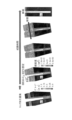
- FIG. 21 is a diagram showing calculation results of coverage and film density distribution by the CVD process.
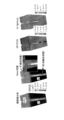
- FIG. 22 is a diagram showing the results of the distribution of the bonded state/unbonded state of Voxel and the gas flux distribution.
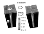
- FIG. 23 is a diagram showing calculation results of water permeability distribution.
- FIG. 24 is a diagram showing calculation results of adhesion distribution.
- FIG. 25 is a diagram showing calculation results of the film density distribution after annealing.
- FIG. 26 is a diagram showing calculation results of adhesion distribution after annealing.
- FIG. 27 is a diagram showing calculation results of water permeability distribution after annealing.
- FIG. 28 is a diagram showing the concept of blister calculation.
- FIG. 29 is a diagram showing an example of a trench crossing structure.
- FIG. 30 is a diagram illustrating a modified example of the processing procedure of FIG. 1.
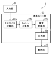
- FIG. 31 is a diagram illustrating a configuration example of a film deposition simulation program according to an embodiment of the present disclosure.
- FIG. 32 is a diagram illustrating a configuration example of a film forming apparatus according to an embodiment of the present disclosure.
- the film deposition simulation method according to this embodiment deals with a film deposition method in which raw material particles are projected onto a processed surface (film deposition surface) to form a film made of raw material particles.
- the film deposition simulation method deals with various vapor deposition methods and predicts the coverage and film quality of the deposited film.
- film formation methods that can be handled by the film formation simulation method according to the present embodiment include physical vapor deposition such as resistance heating evaporation, electron beam evaporation, molecular beam epitaxy, ion plating, and sputtering.
- Chemical Vapor Deposition (CVD) such as physical vapor deposition (PVD), thermal or plasma chemical vapor deposition, atomic layer deposition (ADL), and metal-organic vapor phase deposition. I can give an example.
- the raw material particles are, for example, atoms, molecules, or ions obtained by dissociating these.
- the raw material particles may be formed by decomposing or ionizing the raw material gas introduced into the film forming chamber using heat, plasma, etc., or may be formed by colliding rare gas atoms etc. with a metal target. .
- the number of raw material particles may be one type or two or more types. That is, the film may be a film formed from a single raw material, or a film formed by reacting a plurality of raw materials.
- the target for film formation is, for example, a metal substrate, a semiconductor substrate, a glass substrate, a quartz substrate, or a resin substrate.
- the shape and material of the surface to be film-formed are not particularly limited.
- a thin film or a fine structure may be formed on the surface of the object to be film-formed.
- the film formed on the film-forming target is, for example, a thin film with a thickness of about several micrometers.
- the size of the area that can be handled by the film deposition simulation method according to the present embodiment is, for example, an area with a side length of approximately several micrometers.
- the film deposition simulation method in the film deposition method described above, it is possible to predict the coverage and film quality of the film to be deposited within a range of several tens of nanometers.
- FIG. 1 is a flowchart showing an overview of the flow of the film deposition simulation method according to the present embodiment.
- FIG. 2 is a flowchart showing the flow of the film deposition simulation method shown in FIG. 1 in more detail.
- FIG. 3 is a diagram showing an example of the configuration of an information processing device (film formation simulator) for realizing this film formation simulation method.
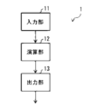
- the film deposition simulator 1 shown in FIG. 3 includes an input section 11, a calculation section 12, and an output section 13.
- the input unit 11 acquires film forming conditions when performing a predetermined film forming process on the film forming surface and inputs the obtained film forming conditions to the calculation unit 12 .
- the input unit 11 includes a GUI (Graphical User Interface) or a CUI (Character-based User Interface) for setting film forming conditions.
- the calculation unit 12 calculates the shape evolution of the film formation surface and the film quality based on the film formation conditions input through the input unit 11 by a simulation method shown in FIGS. 1 and 2, which will be described later.
- the calculation unit 12 may be configured with hardware to implement the calculation processing described later, but the calculation processing may also be performed using a predetermined simulation program (software).
- the calculation unit 12 is configured with a calculation device such as a CPU (Central Processing Unit), reads a simulation program from the outside, and executes the calculation by executing the program.
- a CPU Central Processing Unit
- the simulation program can be stored, for example, in a database (not shown) or a separately provided storage unit such as a ROM (Read Only Memory).
- the simulation program may be installed in advance in, for example, a database or a separately provided storage unit, or may be installed externally in, for example, a database or a separately provided storage unit.
- the simulation program may be distributed from a medium such as an optical disk or a semiconductor memory, or may be downloaded via a transmission means such as the Internet.
- the output unit 13 outputs the calculation result of the calculation unit 12 (the simulation result of a predetermined film forming process calculated by the calculation unit 12).
- the output unit 13 includes a GUI for visualizing the calculation results of the calculation unit 12 (simulation results of a predetermined film forming process calculated by the calculation unit 12). Note that at this time, the output unit 13 may output information such as the film-forming conditions and parameters used in the calculation, along with the simulation results of the film-forming process.
- the output unit 13 is configured by, for example, any one of devices such as a display device that displays simulation results, a printing device that prints and outputs simulation results, and a recording device that records simulation results, or an appropriate combination of these devices. be done. Note that in this embodiment, an example in which the simulator includes the output unit 13 will be described, but the present technology is not limited to this, and the output unit 13 may be provided outside the simulator.
- This simulator may further include a database unit that stores various parameters necessary for calculation processing in the calculation unit 12. Further, such a database section may be provided outside the simulator. Note that if various parameters required for calculation processing are input from the outside at any time, the database section may not be provided.
- a Voxel model based on the flux method is used as a prediction technique for film formation processing.
- the Voxel placed within the calculation area is a cube.
- the Voxel includes not only the presence information of whether or not a film is present, but also the coverage of the film and the film quality (e.g., density, defect density, water permeability, adhesion, etc.). ) information is also included.
- the gas flux flowing into the Voxel includes not only the gas component directly incident (direct incident component), but also the gas component coming from the surrounding pattern (incoming flux into the surrounding structure).
- Calculations also take into account gas surrounding components. Furthermore, using the concept of representative particles depending on the incident flux, the presence of a film, coverage, and film quality are predicted. This makes it possible to accurately predict the presence of a film, coverage, and film quality within a range of several tens of nanometers with lower calculation costs than fluid calculations using the Monte Carlo method.
- the calculation unit 12 sets initial conditions for film formation (step S101, FIGS. 1 and 2).
- the initial conditions for film formation include information regarding the film formation conditions, information regarding the base layer, and the like.
- the film formation method is a vapor deposition method using gas as a raw material
- step S101 model parameters related to surface reaction, incident gas flux, incident energy and angular distribution of ions, etc. are set as information regarding the film formation conditions.
- the material and shape of the base layer may be set as the information regarding the base layer.
- the calculation unit 12 selects the surface Voxel (step S201, FIG. 2).
- the air region (Air) Voxel adjacent to the Voxel of the deposited film deposited in the previous time step is defined as the surface Voxel, and this surface Voxel is used for incident radical flux calculation and surface reaction calculation (adhesion calculation). , desorption, migration, deposition).
- the calculation unit 12 calculates the incident radical flux (step S102, FIGS. 1 and 2). If normal fluid calculations are performed sequentially, the calculation cost is high, and application to micrometer-order patterns handled in semiconductor processes is not realistic. Therefore, in this embodiment, the calculation unit 12 calculates the gas component by dividing it into two parts: the gas component that directly enters the surface Voxel (direct incident component), and the gas component that comes around from the surrounding pattern (surrounding component). I do.
- Pattern A has a larger width than pattern B.
- CB is the direct incident component (density).
- C B depends on the solid angle when looking at the pattern frontage from the surface Voxel. However, the solid angle contribution of adjacent patterns is not included.
- CA is a wraparound component (density).
- the calculation unit 12 calculates C A using the following equations (1) to (3). From the equation of continuity (Equation (1)) and Bernoulli's theorem (Equations (2) and (3)), the gas flowing from pattern A (pattern with large width) to pattern B (pattern with small width) at the connection surface The quantity CA can be determined.
- S A is the opening area of pattern A.
- S B is the area of the connection surface between pattern A and pattern B.
- V A is the gas thermal velocity in pattern A
- V B is the gas thermal velocity in pattern B
- V is a general term for VA and V B
- K B is Boltzmann 's constant
- T N is the gas temperature
- M is the gas mass
- P A is the The pressure of the direct incident component
- P B is the pressure of the circular component.
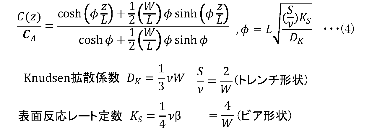
- the calculation unit 12 calculates the contribution component C(z) of CA to the corresponding Voxel from the following equation (4).
- the area from the connection surface S B to the black circle in pattern B is approximately regarded as a partial trench (area expressed by a dot pattern), and C(z) can be approximately calculated from equation (4) below. You can ask for it.
- W is the trench width
- L is the distance from the connection surface to the boundary of pattern B on the opposite side.
- the total flux F at the corresponding Voxel can be calculated from the following equation (5). This total flux F corresponds to the incident radical flux at the corresponding Voxel.
- C(z) is calculated by multiplying C(z) obtained for each surrounding pattern by 1/L. ), and by adding the obtained weighting values (C(z) ⁇ 1/L), the total flux F at the corresponding Voxel can be determined.
- FIG. 4 shows a conceptual diagram of an actual film-forming surface (for example, an O2 step after the BDEAS step of ALD-SiO2).
- FIG. 6 shows a conceptual diagram in which the conceptual diagram of FIG. 5 is translated into a Voxel model.
- a film is formed by repeating adhesion, migration, and deposition as each incident particle bonds with surface particles and causes changes in potential.
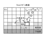
- this algorithm in order to greatly reduce the calculation load, multiple incident particles are represented as one representative particle, which simplifies the handling of radical fluxes of ⁇ 10 18 [/cm 2 /S], and For particles, we deal with adhesion, desorption, migration, and deposition using probabilities. This is an application of the so-called statistical ensemble method.
- the calculation unit 12 calculates the number N of representative particles to be generated for each Voxel.
- the number N of representative particles generated we set the temporary density ⁇ [particles/cm 3 ] of the deposited film, and set the number N of representative particles to 1 Voxel (for example, the number surrounded by the bold frame in Fig. 7) with the volume L 3 ⁇ 10 -21 [cm 3 ].
- the number N of representative particles generated varies depending on the incident radical flux F [numbers/cm 2 /s] within the pattern.
- the calculation unit 12 performs this calculation for each type of radical particle.
- the calculation unit 12 calculates the number N of representative particles generated for each gas within the same time step.
- the calculation unit 12 calculates the number N of representative particles generated at different time steps for each gas.
- the calculation unit 12 determines attachment and detachment for each representative particle (step S104, FIGS. 1 and 2). Specifically, for each representative particle, it is determined using random numbers whether it will adhere with a probability of attachment Y (0 ⁇ Y ⁇ 1) or detach with a probability of (1 ⁇ Y).
- the representative particles are in contact with the base layer (at the very beginning of film formation)
- the influence of variation in the adhesion probability Ys due to the damage Da to the base due to processing is taken into account (Equation (7)).
- the adhesion probability Yd is constant on the deposited film (Equation (8)).
- a, b, and c are constants set by the user. Da is given a result calculated by another film-forming simulator or an experimental value. If desorption is determined, no further surface reaction calculations are performed.
- the calculation unit 12 determines the migration range (step S105, FIGS. 1 and 2).
- FIG. 8 shows a conceptual diagram of the actual film-forming surface during migration and deposition.
- FIG. 9 shows a conceptual diagram of the Voxel model during migration and deposition.
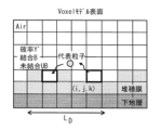
- the attached radical particles migrate on the surface using the energy of the substrate temperature. Radical particles combine with the deposited film (film forming surface) in a region where the surface potential is stable, and the film is deposited. At this time, dangling bonds also exist in some radical particles (Figure 8). When Voxel modeling this phenomenon, consider the following.
- the 2L D cubic range (migration range) of the migration length L D (formula (9)) calculated depending on the substrate temperature T and activation energy Ed is determined (step S105, FIGS. 1 and 2). .
- a cradle (a concavity with a small radius of curvature) is searched within the 2LD cubic range (FIG. 9).
- D 0 is a diffusion constant
- ⁇ is a time constant
- K B is Boltzmann's constant.
- ⁇ D 0 ⁇ and Ed on the right side of equation (9) are parameters whose values are determined from first-principles calculations or actually measured correlations between substrate temperature and film density (slope Ed, y-intercept ⁇ D 0 ⁇ ), etc. .
- the surface potential ⁇ is expressed as in equation (10) using the radius of curvature 1/R. It is assumed that the radical particles migrate so as to minimize the surface potential ⁇ , that is, so that structures (cradle) with a small radius of curvature 1/R are eliminated.
- ⁇ 0 is the chemical potential in a flat film
- ⁇ is the surface tension
- ⁇ is the atomic volume
- 1/R is the radius of curvature.
- the calculation unit 12 identifies Cradle in the Voxel space (Step S202, FIG. 2). Specifically, as shown in Fig. 10, we focused on the Air Voxel (center of gravity coordinates: i, j, k) that is in contact with the deposited film within the migration range (2L D ) surrounded by a thick frame. The materials of the upper, lower, left, and right Voxels adjacent to the Air Voxel are determined. If a Voxel adjacent to the Air Voxel of interest corresponds to a deposited film, 1 is added to the determination index: Nv(i, j, k) of the Air Voxel of interest. The Air Voxel of interest is determined as follows according to the value of the determination index Nv.
- the calculation unit 12 moves the representative particle (step S203, FIG. 2). Specifically, if there is an Air Voxel with Nv ⁇ 3 within the migration range, the representative particle (Gas 1, for example, BDEAS in the ALD-SiO 2 process) will migrate to that Voxel, and in that Voxel, the bond determination will be performed.
- the flag for: F B (i, j, k) is set to 1. If there are multiple Cradles within the migration range, F B (i, j, k) is set to 1 in the Cradle closest to the representative particle (FIG. 11).
- the calculation unit 12 executes the above steps S104 to S106 for all the generated representative particles until the deposition positions are determined (step S204; N).
- the calculation unit 12 selects (determines) the deposition position of representative particles of gas 1 (for example, BDEAS). ), then the attachment/desorption/movement of representative particles of gas 2 (for example, O 2 ) and the selection (determination) of the deposition position are performed (steps S205, S206). That is, film formation is performed by ALD.
- the calculation unit 12 uses random numbers to change the state at the time of deposition to the bonded state ( It is determined whether the probability is Y B ) or the unbonded state (dangling bond system: probability (1-Y B )).
- the calculation unit 12 determines that the state at the time of deposition is an uncombined state (step S208). Note that when determining the state of a Voxel, when ions are incident on the Voxel (that is, when there is an incident ion flux ⁇ i ), the calculation unit 12 determines the state of the Voxel based on the flux and energy of the incident ion. Determine the effect of binding enhancement by ions (determination of bound and unbound).
- the representative particles are deposited in a bonded state with probability Y B .
- the bond state is expressed as the probability Y B ' (user-set value).
- the calculation unit 12 determines the film state (bonded, unbonded) of the Voxel (step S209). In other words, the deposition is calculated as a Voxel in which the representative particle and the film-forming surface are either bonded or unbonded.
- the calculation unit 12 executes steps S205 to S209 described above until the film state (bonded, unbonded) is determined for all Voxels within the migration range (step S210; N).
- the calculation unit 12 determines the film state (bonded, unbonded) for all Voxels within the migration range (step S210; Y)
- it performs shape evolution. Specifically, a Voxel whose film state is bonded is recognized as a deposited film, and a Voxel whose film state is unbonded is recognized as an unbonded film (defect film). In this way, the film is stacked up and its shape changes at each time step.
- the calculation unit 12 performs film quality calculation (step S110, FIGS. 1 and 2). Calculate the distribution of membrane density, water permeability, and adhesion as membrane properties.
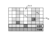
- the membrane morphology shown in Figure 12 the information on the bound state (B) and unbound state (UB) given to each Voxel, as well as the Void region, was averaged within the setting range shown in the thick frame.
- film density, water permeability, and adhesion to the film-forming surface are calculated.
- the coverage and film quality of the film on the film-forming surface are expressed by calculating the deposition as a Voxel that gives state information of either bonding or non-bonding between the representative particle and the film-forming surface.
- the setting range is a parameter set by the user, and is, for example, 100 nm.
- the calculation unit 12 gives a density weight W to each Voxel within the setting area of FIG. 13, and defines the total average of these as the local film density DL (l, m, n) (Equation (13)).
- the density weight W is set to W B in the combined Voxel, W UB in the uncombined Voxel, and W V in the Voxel in the Void region.
- l, m, and n are the barycenter coordinates of the set area
- Q is the number of Voxels in the set area.
- D L0 is separately obtained from actual measurements under typical process conditions, or from MD calculations or the like.
- D L0 is a parameter input by the user.
- the calculation unit 12 calculates the ratio of the volume V v of the Void region within the set region in FIG. 13 to the volume V tot of the set region in FIG. 13 as (an index of) the water permeability WP (Equation (14)). Note that l, m, and n are the barycenter coordinates of the setting area.
- the calculation unit 12 targets the Voxels in contact with the base layer, and calculates the volume V UB of uncombined Voxels (UB) in the setting area in FIG. 14 and the volume V tot of the setting area in FIG. 14.
- the ratio is calculated as an index of adhesion (Equation (15)).
- l, m, n are barycentric coordinates of the setting area.
- the calculation unit 12 After calculating the film quality in this manner, the calculation unit 12 advances the time during calculation by the time step dt (step S211). Then, if the calculation time has not reached the predetermined processing time (step S212; N), the calculation unit 12 continues to execute each step after step S201 described above. On the other hand, if the calculation time reaches the predetermined processing time (step S212; Y), the calculation unit 12 ends the film formation process, and then performs film quality calculation by an annealing process (step S111).
- the calculation unit 12 calculates the thermal denaturation of the film due to annealing, that is, the film density when annealing is performed.
- FIG. 15 shows a conceptual diagram of changes in film morphology and density due to annealing.
- the diffusion length La is calculated according to the substrate temperature T, and the density ⁇ (I, J, K) is equally distributed to the Na Voxels including Air within the 2La range indicated by the thick frame in FIG. .
- representative particles are diffused from the Voxel with the black dot in FIG. 15 to other Voxels within the 2La range indicated by the thick frame in FIG. 15 (FIG. 16).
- equation (8) is used to calculate the diffusion length La.
- the parameter values in equation (8) are different from the parameter values used when calculating the migration length LD .
- the density ⁇ a after annealing is expressed as follows.
- ⁇ a in equation (18) is multiplied by a correction term ⁇ that depends on the substrate temperature T.
- A is a coefficient
- E a is activation energy
- K B is Boltzmann's constant.
- the state is changed to a B (bonded state) Voxel.
- the Voxel that was Air if it becomes larger than the density setting threshold (user setting), it is set as the deposited film Voxel, and the same process is performed for its bonding state. The above calculation is performed for all Voxels except the base Voxel.
- the calculation unit 12 performs the following calculation for the UB (unbonded state) Voxel in the deposited film as a blister (film peeling) calculation immediately after the film formation process or immediately after annealing (when annealing is performed). Performs the Voxel movement process described below.
- the gas density nB of the blister factor in UB is calculated.
- the factor gas flux F B is also derived (hydrogen (H) in the case of SiO 2 film formation) and stored in the Voxel.
- the Voxel size L, the film formation time t, and the number N S of superparticles is expressed by the following equation (19).
- Equation 19 the energy of the gas pressure can be calculated using the following equation: It is expressed as (20).
- T is the substrate temperature during film formation.
- P B (L 3 ) is compared with the total sum E Btot of the binding energies of the Voxel adjacent surfaces, which is shown by a thick solid line that straddles the thick frame in FIG. 17, and P B (L 3 ) is larger than the total sum E Btot .
- each Voxel surrounded by a thick frame in FIG. 17 is moved up one level, and its original location is set to Air (FIG. 18).
- the sum of the binding energies of P B (L 3 ) and the Voxel adjacent surfaces shown by the thick solid line that straddles the thick frame in FIG. 19 the thick frame surrounding the Voxel adjacent to the outside of the thick frame in FIG. 17).
- E Btot is approximately expressed as follows using the areal density ⁇ of adjacent Voxels and the average binding energy E B .
- R B in order to reflect the influence of ions on bond formation during film deposition, a correction term dependent on ion energy E: exp (-E 0 /E) x 2.718 is applied. Use the value given.
- E 0 is the reference ion energy.
- ⁇ Effect> In the film deposition simulation method and film deposition simulator 1 according to the present embodiment, representative particles are generated according to the incident radical flux, and the attachment, desorption, migration, and deposition of each representative particle on the film deposition surface are calculated based on probability. is executed. This makes the accuracy and calculation time independent of the number of particles.
- the deposition is calculated as a Voxel with state information of either bonding or unbonding between the representative particle and the film-forming surface. The nature and membranous quality are expressed. This eliminates the need to separately prepare a database dependent on morphology and gas flux for film quality calculations. Therefore, calculation time can be shortened and calculation accuracy can be improved. Furthermore, it is expected that the TAT until utilization of this algorithm will be shortened.
- the incident radical flux is reduced by a gas component that is directly incident on the Voxel on the film-forming surface and a gas wraparound component that is incident on the Voxel on the film-forming surface according to the surrounding structure. Calculated. Thereby, it is possible to improve calculation accuracy that reflects the actual structure.
- the film density, water permeability, and adhesion to the film-forming surface are calculated using either bonded or unbonded state information. This makes it possible to realize a film formation process with higher precision.
- the number of representative particles generated for each gas is calculated within the same time step. This makes it possible to express a film forming process by CVD or PVD.
- the number of generated representative particles is calculated at separate time steps for each gas. This makes it possible to express the film formation process by ALD.
- the input section 11 is configured by a GUI or CUI for setting film deposition conditions
- the output section 13 is configured by a GUI for visualizing the calculation results in the calculation section 12. has been done.
- the user can operate the film-forming simulator 1 relatively easily, and can understand the calculation results by the film-forming simulator 1 relatively easily.
- FIG. 21 shows calculations of coverage and film density distribution by the CVD process according to this example.
- the substrate temperature was 800° C.
- the gas pressure was 400 Pa
- the film was formed on the underlying Si trench using BDEAS and O 2 gases.
- the base Si trench has a structure in which two trenches each having a line width of 150 nm, a depth of 2 ⁇ m, and a depth of 450 nm intersect.
- Figure 21 shows the adhesion probability (0.5 + 0.5 ⁇ Da) reflecting the process damage generated during trench etching and the probability of Voxel bonding state during deposition due to incident ions (maximum energy of 50 eV) (ion incidence).
- the simulation results are shown in which 0.2 is taken into account when there is no difference, and 1) is taken into account when there is.
- Activation energy (migration, determination of bonding state by ion injection) was uniformly set to 0.4 eV.
- the Voxel size is 5 nm, and the averaging setting range used in film quality calculation is 25 nm.
- the incident ion flux to the pattern is 4 ⁇ 10 16 /cm 2 /s
- the radical (BDEAS, O 2 ) flux is 1 ⁇ 10 18 /cm 2 /s.
- the slit region of the trench is closed, and a thin layer of SiO 2 is deposited inside the trench, forming a void. Further, the film density is high in the flat part that is strongly affected by ion irradiation (the probability that the Voxel is determined to be in a bonded state is high), and the film density is low inside the trench where it is less affected.
- the results of the distribution of the bonded state/unbonded state of Voxel and the gas flux distribution are shown in FIG. 22.
- FIG. 23 shows the calculation results of the water permeability distribution according to this example. These are calculation results using the film formation conditions and underlying structure of Example 1. Water permeability is low in the flat area, and higher inside the trench.
- FIG. 24 shows the calculation results of the adhesion distribution according to this example. These are calculation results using the film formation conditions and underlying structure of Example 1. The adhesion is high in the flat portion, and is lower inside the trench.
- Example 4 ⁇ Basic CVD calculation (annealing) ⁇ Results of annealing calculations according to this example are shown in FIGS. 25, 26, and 27. Changes in film density distribution (Figure 25), adhesion distribution (Figure 26), and water permeability distribution (Figure 27) when 1100°C annealing was performed after film formation in Example 1. The calculation result is an improvement.
- Example 5 ⁇ Basic CVD calculation (blister) ⁇ A conceptual diagram of the blister calculation according to this embodiment is shown in FIG. Blister calculation was performed after film formation in Example 1.
- the binding energy is 5 eV
- blisters (film peeling) equivalent to two Voxel layers are formed on the flat part. The result was that
- Example 6> ⁇ Applied CVD calculation (pattern with wide line width + pattern with narrow line width)
- pattern with wide line width + pattern with narrow line width an example of an intersecting structure of two trenches having the same line width was used.
- the calculation by this algorithm is not limited to this, and can be applied to any structure in which a pattern with a wide line width and a pattern with a narrow line width are mixed together.
- calculations using this algorithm can be performed on a pattern composed of a circular pattern B and four rectangular patterns A connected around it.
- calculations using this algorithm can be performed on a pattern composed of a rectangular pattern B and four rectangular patterns A connected around it. I can do it.
- a circular pattern B and two patterns connected to each other at positions facing each other via the circular pattern B are connected to each other. Calculations using this algorithm can be performed on a pattern formed by the shape pattern A.
- a rectangular pattern B and two patterns connected to each other at positions facing each other via the rectangular pattern B are connected to each other. Calculations using this algorithm can be performed on a pattern formed by the shape pattern A.
- a circular pattern B and two rectangular shapes connected around the circular pattern B at positions where their extension directions intersect at 90° are also available.
- This algorithm can perform calculations on a pattern formed by pattern A and pattern A.
- a rectangular pattern B and two rectangular shapes connected to each other at a position around the rectangular pattern B and whose extension directions intersect with each other at 90° are also available. This algorithm can perform calculations on a pattern formed by pattern A and pattern A.
- Example 7 ⁇ ALD calculation ⁇ Examples 1 to 6 show CVD calculations.
- the coverage and film quality can be calculated as an ALD process by repeating the calculations regarding gas 1 and gas 2 in FIG. I can do it.
- Examples 1 to 6 show CVD calculations.
- Examples 1 to 6 show CVD calculations.
- FIG. 31 shows a configuration example of information processing software (film formation simulation program) for realizing the film formation simulation method shown in FIGS. 1 and 2.
- the film deposition simulation program 2 shown in FIG. 31 includes an input section 21, an arithmetic engine section 22, and a display section 23 for visualizing simulation results.
- the calculation engine section 22 includes a gas flux calculation section 22a, a coverage calculation section 22b, a film quality calculation section 22c, and an output section 22d.
- the input unit 21 is configured by a GUI (Graphical User Interface) or CUI (Character-based User Interface) for setting initial conditions.
- the input unit 21 outputs the set initial condition value to the calculation engine unit 22.
- the display section 23 is configured with a GUI for visualizing the data obtained from the output section 22d.
- the gas flux calculation unit 22a calculates the incident radical flux that is incident on the surface Voxel by executing the above-mentioned step S102 using the value of the initial condition set by the input unit 21.
- the coverage calculation unit 22b calculates the shape and state of the film by executing steps S103 to S109 described above using the value of the incident radical flux calculated by the gas flux calculation unit 22a.
- the film quality calculation section 22c calculates the film quality by executing steps S110 and S111 described above based on the shape and state of the film obtained by the coverage calculation section 22b.
- the output unit 22d outputs simulation results of a predetermined film forming process calculated by the coverage calculation unit 22b and the film quality calculation unit 22c.
- the execution platform of this film deposition simulation program 2 may be, for example, Windows (registered trademark), Linux (registered trademark), Unix (registered trademark), or Mac (registered trademark).
- the GUI used in the input unit 21 and the display unit 23 may be configured in any language such as OpenGL, Motif, or tcl/tk.
- the programming language of the arithmetic engine unit 22 is not limited to C, C++, Fortran, JAVA (registered trademark), or the like.
- This film deposition simulation program 2 may have a function of taking in calculation results by other simulators and passing them to the calculation engine section 22.
- the output unit 22d outputs the material and coordinates of each Voxel, the bonding state, membrane quality (membrane density, water permeability, adhesion), and surface flux of each Voxel. is output to a file or temporary storage area. Visualization of these results is performed using the GUI. Data output and visualization may be performed in real time during calculation.
- representative particles are generated according to the incident radical flux, and calculations of attachment, desorption, migration, and deposition of each representative particle on the film forming surface are performed based on probability.
- the deposition is calculated as a Voxel that gives information on the state of either bonding or unbonding between the representative particle and the film-forming surface, thereby improving the film coverage on the film-forming surface. and membrane quality are expressed. This eliminates the need to separately prepare a database dependent on morphology and gas flux for film quality calculations. Therefore, calculation time can be shortened and calculation accuracy can be improved. Furthermore, it is expected that the TAT until utilization of this algorithm will be shortened.
- the input section 21 is configured by a GUI or CUI for setting film forming conditions
- the output section 22d is configured by a GUI for visualizing the calculation results in the coverage calculation section 22b and the film quality calculation section 22c. ing.
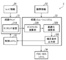
- FIG. 32 shows an example of the configuration of a film forming apparatus 3 to which the film forming simulation method (film forming simulation program 2) shown in FIGS. 1 and 2 is applied.
- the film forming apparatus 3 includes a film forming chamber 31, a film forming simulation system 32, a control system 33, and an FDC/EES (Fault Detection and Classification/Equipment Engineering System) system 34.
- FDC/EES Fault Detection and Classification/Equipment Engineering System
- the film forming chamber 31 has a monitoring device 31A that monitors the state inside the chamber.
- the monitoring device 31A has, for example, OES (Optical Emission Spectroscopy).
- OES is a measurement device that monitors light emission from plasma within a chamber. During film formation, light with a unique wavelength is emitted for each gas species present in the plasma. OES measures that light. OES measures the emission intensity for each wavelength. The OES specifies the gas type from the measured wavelength and outputs information about the specified gas type as monitoring data.
- the monitoring device 31A includes, for example, a system for monitoring the state inside the chamber. This system measures temporal fluctuations in gas pressure, flow rate, temperature, power, bias, matcher capacity, vacuum pump opening degree, etc., and outputs the data obtained from the measurements as monitoring data.
- the film-forming chamber 31 transmits data (monitoring data) obtained by the monitoring device 31A to the film-forming simulation system 32.
- the deposition simulation system 32 includes a deposition simulator 1 that executes a deposition simulation program 2.
- the film deposition simulation system 32 includes a gas flux calculation section 32A, an optimization calculation section 32B, and a correction condition output section 32C.
- the gas flux calculation unit 32A, the optimization calculation unit 32B, and the correction condition output unit 32C may be configured by an integrated circuit, or may be configured by a calculation device loaded with the film deposition simulation program 2.
- the gas flux calculation unit 32A calculates the incident radical flux using the monitoring data input from the monitoring device 31A.
- the optimization calculation unit 32B uses the value of the incident radical flux obtained by the gas flux calculation unit 32A to execute steps S103 to S109 described above, thereby generating representative particles according to the value of the incident radical flux. , the adhesion, desorption, migration, and deposition of each representative particle on the film-forming surface are calculated based on the probability. As a result, the optimization calculation unit 32B can predict the shape and state of the film.
- the optimization calculation unit 32B further calculates the film quality by executing steps S110 and S111 described above based on the shape and state of the obtained film.
- the optimization calculation unit 32B compares the calculated value (predicted value) obtained in this way with the desired specifications (for example, the set film thickness information D2), and determines whether the calculated value (predicted value) is within the allowable range. If the calculated value (predicted value) falls within the allowable range, optimization conditions for the film forming process are searched for. Specifically, the optimization calculation unit 32B changes the gas flow rate, gas pressure, substrate temperature, and processing time to find a solution using a predetermined algorithm. The optimization calculation unit 32B searches for optimization conditions for each wafer or for each lot.
- the optimization calculation unit 32B transmits an abnormality signal to the FDC/EES system 34.
- the FDC/EES system 34 receives an abnormal signal from the optimization calculation unit 32B, it outputs a signal to the control system 33 to stop the operation of the film forming chamber 31.
- the control system 33 receives a signal to stop the operation of the film forming chamber 31, the control system 33 stops the operation of the film forming chamber 31.
- the optimization calculation section 32B outputs the found optimization condition to the correction condition output section 32C.
- the correction condition output unit 32C When the optimization conditions are input, the correction condition output unit 32C generates data necessary for the film formation conditions of the film formation chamber 31 to become the optimization conditions, and outputs the data to the control system 33.
- the control system 33 receives the data necessary for optimizing the conditions, it controls the operation of the deposition chamber 31 based on the received data. Control system 33 modifies recipe information D1 based on the received data.
- the optimization calculation unit 32B if the calculation time is on a scale equal to or greater than the actual machining time, instead of finding the optimal solution online as described above, it performs simulations in advance using this algorithm for various process conditions.
- a database is created in advance, and representative particles are generated according to the value of the incident radical flux by executing steps S103 to S109 described above using the value of the incident radical flux predicted using the database. Any method (offline method) is also acceptable.
- a machine learning model may be constructed using a database, and the model may be used as the online optimization calculation unit 32B.
- representative particles are generated according to the incident radical flux, and calculations of attachment, desorption, migration, and deposition of each representative particle on the film forming surface are performed based on probability.
- the deposition is calculated as a Voxel that gives information on the state of either bonding or unbonding between the representative particle and the film-forming surface, thereby improving the film coverage on the film-forming surface. and membrane quality are expressed. This eliminates the need to separately prepare a database dependent on morphology and gas flux for film quality calculations. Therefore, calculation time can be shortened and calculation accuracy can be improved. Furthermore, it is expected that the TAT until utilization of this algorithm will be shortened.
- optimization conditions for the film forming process are searched based on the calculation results obtained by the above calculation, and the film forming conditions of the film forming chamber are changed to the found optimization conditions.
- the data necessary to achieve this is generated and output to the control system 33. Such feedback makes it possible to manufacture higher quality semiconductor devices.
- the state inside the film forming chamber is monitored by the monitoring device 31A, and the incident radical flux is calculated using the monitoring data obtained by the monitoring device 31A.
- representative particles are generated according to the value of the incident radical flux predicted using a database.
- the calculation time is on a scale equal to or greater than the actual processing time, it is possible to manufacture semiconductor devices of higher quality.
- optimization conditions are searched for each wafer or each lot. This makes it possible to manufacture higher quality semiconductor devices on a wafer-by-wafer or lot-by-lot basis.
- the present disclosure can take the following configuration.
- (1) A first step of generating representative particles according to the incident radical flux and calculating attachment, desorption, migration, and deposition of each representative particle on the film-forming surface according to probability, In the first step, the coverage and film quality of the film on the film-forming surface are calculated by calculating the deposition as a Voxel with information on whether the representative particle is bonded or unbonded to the film-forming surface. Deposition simulation method including representation.
- (2) A gas component that directly enters the Voxel in the air region adjacent to the film forming surface, and a gas component that enters the Voxel in the air region adjacent to the film forming surface depending on the surrounding structure.
- the film deposition simulation method according to (1) further comprising a second step of calculating the incident radical flux based on the components.
- (3) In the first step, it is determined whether or not the representative particle is bonded to the film-forming surface based on the flux and energy of ions incident on the Voxel in the air region adjacent to the film-forming surface.
- the first step further includes calculating film density, water permeability, and adhesion to the film-forming surface using the state information. Membrane simulation method.
- any one of (1) to (3) further includes calculating the number of representative particles generated for each gas within the same time step. 1.
- any one of (1) to (3) further includes calculating the number of generated representative particles at separate time steps for each gas. 1.
- the calculation unit expresses the coverage and film quality of the film on the film-forming surface by calculating the deposition as a Voxel that gives state information of either bonding or non-bonding between the representative particle and the film-forming surface.
- a film deposition simulation program (9)
- the input unit is configured by a GUI (Graphical User Interface) or a CUI (Character-based User Interface) for setting film forming conditions,
- the calculation unit expresses the coverage and film quality of the film on the film-forming surface by calculating the deposition as a Voxel that gives state information of either bonding or non-bonding between the representative particle and the film-forming surface.
- Deposition simulator is
- the input unit is configured by a GUI (Graphical User Interface) or a CUI (Character-based User Interface) for setting film forming conditions,
- the film-forming simulator according to (10) wherein the output section is configured with a GUI for visualizing the calculation results in the calculation section.
- a deposition chamber ; a control unit that controls the operation of the film forming chamber; Representative particles are generated according to the value of the incident radical flux, and the adhesion, desorption, migration, and deposition of each representative particle on the film-forming surface are calculated based on the probability, and based on the calculated results, the formation an optimization calculation unit that searches for optimization conditions for the membrane process; an output unit that generates data necessary for the film formation conditions of the film formation chamber to become the optimization conditions found in the optimization calculation unit, and outputs the data to the control unit;
- the optimization calculation unit calculates the coverage and film quality of the film on the film-forming surface by calculating the deposition as a Voxel that gives state information of either bonding or non-bonding between the representative particle and the film-forming surface.
- a film deposition system that expresses (13) a monitoring device that monitors the state inside the film forming chamber;
- the optimization calculation unit generates representative particles according to the value of the incident radical flux predicted using a database.
- the optimization calculation unit searches for the optimization condition for each wafer or for each lot.
Landscapes
- Chemical & Material Sciences (AREA)
- Chemical Kinetics & Catalysis (AREA)
- Engineering & Computer Science (AREA)
- Materials Engineering (AREA)
- Mechanical Engineering (AREA)
- Metallurgy (AREA)
- Organic Chemistry (AREA)
- General Chemical & Material Sciences (AREA)
- Physical Vapour Deposition (AREA)
- Chemical Vapour Deposition (AREA)
- Management, Administration, Business Operations System, And Electronic Commerce (AREA)
Abstract
Description
<概略>
まず、本開示の一実施形態に係る成膜シミュレーション方法の概略について説明する。本実施形態に係る成膜シミュレーション方法では、加工表面(成膜表面)に対して、原料粒子を投射し、原料粒子からなる膜を形成する成膜方法を扱う。
続いて、図1、図2を参照して、本実施形態に係る成膜シミュレーション方法の流れの概要について説明する。図1は、本実施形態に係る成膜シミュレーション方法の流れの概要を示すフローチャート図である。図2は、図1に記載の成膜シミュレーション方法の流れをより詳細に示すフローチャート図である。図3は、この成膜シミュレーション方法を実現するための情報処理装置(成膜シミュレータ)の一構成例を示す図である。
図3に示した成膜シミュレータ1は、入力部11と、演算部12と、出力部13とを備えている。入力部11は、成膜表面に対して所定の成膜処理を行う際の成膜条件を取得して演算部12に入力するものである。入力部11は、成膜条件を設定するためのGUI(Graphical User Interface)もしくはCUI(Character-based User Interface)によって構成されている。演算部12は、入力部11を介して入力された成膜条件に基づいて、後述する図1,図2に示したシミュレーション方法によって、成膜表面の形状進展や膜質の計算を行う。
本シミュレーションでは、成膜処理の予測技術として、フラックス法ベースのVoxelモデルが用いられる。一般にVoxelモデルでは、計算領域内に配置するVoxelは立方体となっている。本実施の形態では、Voxelには、膜がそこに存在するか否かの存在情報だけでなく、膜の被覆性(カバレッジ)および膜質(例えば、密度、欠陥密度、透水性、および密着性など)といった情報も含まれる。さらに、本実施の形態では、Voxelに流入するガスフラックス(入射フラックス)は、直接入射してくるガス成分(直接入射成分)だけでなく、周囲のパターンから廻りこんでくるガス成分(周囲構造に応じたガス廻りこみ成分)も考慮して計算する。さらに、入射フラックスに応じた代表粒子という概念を用いて、膜の存在や、被覆性、さらには膜質を予測する。これにより、モンテカルロ法による流体計算と比べて、少ない計算コストで、膜の存在や、被覆性、さらには膜質を数十nmの範囲にて精度良く予測することが可能である。









・Nv=1または2 →着目したAir VoxelはCradleではないと判定する。
フラグ:F(i,j,k)=1とする。
・Nv=0 →着目したAir VoxelはAirのままであると判定する。


演算部12は、図13の設定領域内において、各Voxelの密度重みWを与え、これらの総和平均を局所的な膜密度DL(l,m,n)として定義する(式(13))。密度重みWは、結合VoxelにおいてWBとし、未結合VoxelにおいてWUBとし、Void領域のVoxelにおいてWVとする。なお、l,m,nは設定領域の重心座標、Qは設定領域内のVoxel数である。ただし、DL0は、別途、典型的なプロセス条件によって実測から求められるか、または、MD計算等から求められる。DL0は、ユーザによって入力されるパラメータである。

演算部12は、図13の設定領域内におけるVoid領域の体積Vvと、図13の設定領域の体積Vtotとの比を透水性WP(の指標)として算出する(式(14))。なお、l,m,nは、設定領域の重心座標である。

演算部12は、図14に示したように、下地層に接するVoxelを対象とし、図14の設定領域内における未結合Voxel(UB)の体積VUBと、図14の設定領域の体積Vtotとの比を密着性Ad(の指標)として算出する(式(15))。l,m,nは、設定領域の重心座標である。

ここでは、演算部12は、アニールによる膜の熱変性、つまり、アニールを施した時の膜密度を計算する。アニールによる膜モフォロジーと密度の変化の概念図を図15に示す。まず、基板温度Tに応じた拡散長Laを計算し、図15において太枠で示した2La範囲内にあるNa個の、Airを含むVoxelへ密度ρ(I,J、K)を等分配する。これにより、図15中の黒点のあるVoxelから、図15において太枠で示した2La範囲内にある他のVoxelへ代表粒子を拡散させる(図16)。なお、拡散長Laの計算には、式(8)と同じ式を用いる。ただし、式(8)におけるパラメータ値は、マイグレーション長LDの計算のときのパラメータ値とは異なる。



演算部12は、成膜プロセスが終わった直後、あるいは、アニール直後(アニールを施した時)のブリスター(膜剥がれ)計算として、堆積膜中のUB(未結合状態)のVoxelに対して以下に述べるVoxel移動の処理を行う。


本実施の形態に係る成膜シミュレーション方法および成膜シミュレータ1では、入射ラジカルフラックスに応じた代表粒子が生成され、確率によって成膜表面での各代表粒子の付着、脱離、マイグレーションおよび堆積の計算が実行される。これにより、精度と計算時間が粒子数に依存しなくなる。また、本実施の形態では、上記計算において、代表粒子と成膜表面との結合および未結合のいずれかの状態情報を付与したVoxelとして堆積が計算されることで、成膜表面における膜の被覆性および膜質が表現される。これにより、膜質計算のために、モフォロジーとガスフラックスに依存したデータベースを別途準備する必要がない。従って、計算時間の短縮化および計算精度の向上を図ることができる。また、本アルゴリズムの活用までのTAT短縮が期待される。
~基本のCVD計算(カバレッジ+膜密度)~
本実施例に係るCVDプロセスによるカバレッジと膜密度分布の計算を図21に示す。基板温度が800℃、ガス圧力は400Pa、BDEASとO2のガスによる下地Siトレンチに対する成膜である。下地Siトレンチは、線幅150nm、深さ2μm、奥行き450nmの2つのトレンチが交差した構造となっている。図21には、トレンチエッチング時の生成された加工ダメージを反映した付着確率(0.5+0.5×Da)と入射イオン(最大50eVのエネルギー)による堆積時のVoxel結合状態の確率(イオン入射がない場合には0.2、ある場合には1)を加味したシミュレーション結果が示されている。活性化エネルギー(マイグレーション、イオン入射による結合状態の判定)は一律0.4eVと設定した。Voxelサイズは5nm、膜質計算で用いる平均化の設定範囲は25nmである。また、パターンへの入射イオンフラックスは4×10¹⁶/cm2/s、ラジカル(BDEAS、O2)のフラックスは1×1018/cm2/sである。
~基本のCVD計算(透水性)~
本実施例に係る透水性分布の計算結果を図23に示す。実施例1の成膜条件と下地構造を用いた時の計算結果である。平坦部では透水性は低く、トレンチ内部で透水性がより高くなっている。
~基本のCVD計算(密着性)~
本実施例に係る密着性分布の計算結果を図24に示す。実施例1の成膜条件と下地構造を用いた時の計算結果である。平坦部では密着性は高く、トレンチ内部で密着性がより低くなっている。
~基本のCVD計算(アニール)~
本実施例に係るアニール計算の結果を図25、図26、図27に示す。実施例1の成膜後に、1100℃アニールを施した時の膜密度分布(図25)、密着性分布(図26)、透水性分布(図27)の変化であり、これら膜質がトレンチ内部にかけて改善する計算結果となっている。
~基本のCVD計算(ブリスター)~
本実施例に係るブリスター計算の概念図を図28に示す。実施例1の成膜後に、ブリスター計算を行ったものである。基板温度は800℃、要因ガスフラックスは1×10¹⁸/cm2/s、RB=0.01、結合エネルギーは5eVと設定した場合、平坦部にVoxel2層分のブリスター(膜剥がれ)が形成される結果となった。
~応用CVD計算(線幅が広いパターン+線幅が狭いパターン)
実施例1の計算では2つの同じ線幅のトレンチの交差構造を例にとった計算であった。一方、本アルゴリズムによる計算はそれに限定されるものではなく、線幅が広いパターンと線幅が狭いパターンとが互いに混ざった任意の構造にも応用することができる。
~ALD計算~
実施例1~6ではCVDの計算を示した。一方で、本実施例では、図2でのガス1とガス2に関する計算を成膜終了時間まで設定時間ごと(たとえば、10s)に交互に繰り返すことで、ALDプロセスとしてカバレッジと膜質を計算することができる。
~PVD計算~
実施例1~6ではCVDの計算を示した。一方で、本実施例では、図2でのガス1のみの計算を行うことで単一元素から構成される金属膜ターゲットのPVD計算とすることができる。また、ガス1とガス2、さらにはガス3以降の計算を追加することで、複数元素からなる化合物ターゲットのPVD計算とすることができる。
~気相計算との連携~
本実施例を図30に示す。図1の入射フラックス計算に関して、気相計算を行うことでチャンバ面内でのガス1とガス2の密度分布をシミュレーションする。これら密度分布を入力として、ガスの熱速度を掛けあわせることでフラックスを導出する。気相計算では、上部電極に印加するパワーと周波数、ガス種、ガス流量、ガス圧力、チャンバ壁状態(ガスの付着確率)、チャンバ構成、排気速度をインプットとする。あるいは、実測データベースに基づく補間計算でもよいし、機械学習(たとえば、ガウス過程回帰やディープラーニング等。ただし、手法は限定しない)を用いた計算でもよい。
図1,図2に示した成膜シミュレーション方法を実現するための情報処理ソフトウェア(成膜シミュレーションプログラム)の一構成例を図31に示す。
図31に示した成膜シミュレーションプログラム2は、入力部21と、演算エンジン部22と、シミュレーション結果を可視化するための表示部23とを備えている。演算エンジン部22は、ガスフラックス計算部22a、カバレッジ計算部22bと、膜質計算部22cと、出力部22dとを有している。
図1,図2に示した成膜シミュレーション方法(成膜シミュレーションプログラム2)を適用した成膜装置3の一構成例を図32に示す。
成膜装置3の概念図を図32に示す。成膜装置3は、成膜チャンバ31、成膜シミュレーションシステム32、制御システム33、およびFDC/EES(Fault Detection and Classification/Equipment Engineering System)システム34を備えている。
(1)
入射ラジカルフラックスに応じた代表粒子を生成し、確率によって成膜表面での各前記代表粒子の付着、脱離、マイグレーションおよび堆積を計算する第1ステップを含み、
前記第1ステップにおいて、前記代表粒子と前記成膜表面との結合および未結合のいずれかの状態情報を付与したVoxelとして前記堆積を計算することで前記成膜表面における膜の被覆性および膜質を表現することを含む
成膜シミュレーション方法。
(2)
前記成膜表面に隣接する、空気領域のVoxelに対して直接入射してくるガス成分と、前記成膜表面に隣接する、空気領域のVoxelに対して周囲構造に応じて入射してくるガス回り込み成分とにより、前記入射ラジカルフラックスを算出する第2ステップを更に含む
(1)に記載の成膜シミュレーション方法。
(3)
前記第1ステップにおいて、前記成膜表面に隣接する、空気領域のVoxelに対して入射するイオンのフラックスおよびエネルギーに基づいて、前記代表粒子と前記成膜表面との結合および未結合の判断を行うことを更に含む
(1)または(2)に記載の成膜シミュレーション方法。
(4)
前記第1ステップにおいて、前記状態情報を用いて、膜密度、透水性および前記成膜表面との密着性を計算することを更に含む
(1)ないし(3)のいずれか1つに記載の成膜シミュレーション方法。
(5)
前記第1ステップにおいて、複数種類のガスを用いて成膜を行う場合、同じ時間ステップ内でガスごとの前記代表粒子の生成個数を算出することを更に含む
(1)ないし(3)のいずれか1つに記載の成膜シミュレーション方法。
(6)
前記第1ステップにおいて、複数種類のガスを用いて成膜を行う場合、ガスごとに別々の時間ステップで前記代表粒子の生成個数を算出することを更に含む
(1)ないし(3)のいずれか1つに記載の成膜シミュレーション方法。
(7)
前記第1ステップにおいて、成膜後に、アニールを施した時の膜密度およびブリスターの少なくとも一方を計算することを更に含む
(1)ないし(6)のいずれか1つに記載の成膜シミュレーション方法。
(8)
成膜条件を取得する入力部と、
前記入力部で取得した前記成膜条件に基づいて、入射ラジカルフラックスに応じた代表粒子を生成し、確率によって成膜表面での各前記代表粒子の付着、脱離、マイグレーションおよび堆積を計算する演算部と、
前記演算部での演算結果を出力する出力部と
を備え、
前記演算部は、前記代表粒子と前記成膜表面との結合および未結合のいずれかの状態情報を付与したVoxelとして前記堆積を計算することで前記成膜表面における膜の被覆性および膜質を表現する
成膜シミュレーションプログラム。
(9)
前記入力部は、成膜条件を設定するためのGUI(Graphical User Interface)もしくはCUI(Character-based User Interface)によって構成され、
前記出力部は、前記演算部での演算結果を可視化するためのGUIによって構成されている
(8)に記載の成膜シミュレーションプログラム。
(10)
成膜条件を取得する入力部と、
前記入力部で取得した前記成膜条件に基づいて、入射ラジカルフラックスに応じた代表粒子を生成し、確率によって成膜表面での各前記代表粒子の付着、脱離、マイグレーションおよび堆積計算する演算部と、
前記演算部での演算結果を出力する出力部と
を備え、
前記演算部は、前記代表粒子と前記成膜表面との結合および未結合のいずれかの状態情報を付与したVoxelとして前記堆積を計算することで前記成膜表面における膜の被覆性および膜質を表現する
成膜シミュレータ。
(11)
前記入力部は、成膜条件を設定するためのGUI(Graphical User Interface)もしくはCUI(Character-based User Interface)によって構成され、
前記出力部は、前記演算部での演算結果を可視化するためのGUIによって構成されている
(10)に記載の成膜シミュレータ。
(12)
成膜チャンバと、
前記成膜チャンバの動作を制御する制御部と、
入射ラジカルフラックスの値に応じた代表粒子を生成し、確率によって成膜表面での各前記代表粒子の付着、脱離、マイグレーションおよび堆積を計算し、それにより得られた計算結果に基づいて、成膜プロセスの最適化条件を探索する最適化演算部と、
前記成膜チャンバの成膜条件が、前記最適化演算部で見つかった前記最適化条件となるのに必要なデータを生成し、前記制御部へ出力する出力部と
を備え、
前記最適化演算部は、前記代表粒子と前記成膜表面との結合および未結合のいずれかの状態情報を付与したVoxelとして前記堆積を計算することで前記成膜表面における膜の被覆性および膜質を表現する
成膜装置。
(13)
前記成膜チャンバ内の状態をモニタリングするモニタリング装置と、
前記モニタリング装置により得られたモニタリングデータを用いて前記入射ラジカルフラックスを計算するガスフラックス演算部と
を更に備えた
(12)に記載の成膜装置。
(14)
前記最適化演算部は、データベースを利用して予測した前記入射ラジカルフラックスの値に応じた代表粒子を生成する
(12)に記載の成膜装置。
(15)
前記最適化演算部は、ウェハ毎、または、ロット毎に、前記最適化条件を探索する
(12)ないし(14)のいずれか1つに記載の成膜装置。
Claims (15)
- 入射ラジカルフラックスに応じた代表粒子を生成し、確率によって成膜表面での各前記代表粒子の付着、脱離、マイグレーションおよび堆積を計算する第1ステップを含み、
前記第1ステップにおいて、前記代表粒子と前記成膜表面との結合および未結合のいずれかの状態情報を付与したVoxelとして前記堆積を計算することで前記成膜表面における膜の被覆性および膜質を表現することを含む
成膜シミュレーション方法。 - 前記成膜表面に隣接する、空気領域のVoxelに対して直接入射してくるガス成分と、前記成膜表面に隣接する、空気領域のVoxelに対して周囲構造に応じて入射してくるガス回り込み成分とにより、前記入射ラジカルフラックスを算出する第2ステップを更に含む
請求項1に記載の成膜シミュレーション方法。 - 前記第1ステップにおいて、前記成膜表面に隣接する、空気領域のVoxelに対して入射するイオンのフラックスおよびエネルギーに基づいて、前記代表粒子と前記成膜表面との結合および未結合の判断を行うことを更に含む
請求項1に記載の成膜シミュレーション方法。 - 前記第1ステップにおいて、前記状態情報を用いて、膜密度、透水性および前記成膜表面との密着性を計算することを更に含む
請求項1に記載の成膜シミュレーション方法。 - 前記第1ステップにおいて、複数種類のガスを用いて成膜を行う場合、同じ時間ステップ内でガスごとの前記代表粒子の生成個数を算出することを更に含む
請求項1に記載の成膜シミュレーション方法。 - 前記第1ステップにおいて、複数種類のガスを用いて成膜を行う場合、ガスごとに別々の時間ステップで前記代表粒子の生成個数を算出することを更に含む
請求項1に記載の成膜シミュレーション方法。 - 前記第1ステップにおいて、成膜後に、アニールを施した時の膜密度およびブリスターの少なくとも一方を計算することを更に含む
請求項1に記載の成膜シミュレーション方法。 - 成膜条件を取得する入力部と、
前記入力部で取得した前記成膜条件に基づいて、入射ラジカルフラックスに応じた代表粒子を生成し、確率によって成膜表面での各前記代表粒子の付着、脱離、マイグレーションおよび堆積を計算する演算部と、
前記演算部での演算結果を出力する出力部と
を備え、
前記演算部は、前記代表粒子と前記成膜表面との結合および未結合のいずれかの状態情報を付与したVoxelとして前記堆積を計算することで前記成膜表面における膜の被覆性および膜質を表現する
成膜シミュレーションプログラム。 - 前記入力部は、成膜条件を設定するためのGUI(Graphical User Interface)もしくはCUI(Character-based User Interface)によって構成され、
前記出力部は、前記演算部での演算結果を可視化するためのGUIによって構成されている
請求項8に記載の成膜シミュレーションプログラム。 - 成膜条件を取得する入力部と、
前記入力部で取得した前記成膜条件に基づいて、入射ラジカルフラックスに応じた代表粒子を生成し、確率によって成膜表面での各前記代表粒子の付着、脱離、マイグレーションおよび堆積計算する演算部と、
前記演算部での演算結果を出力する出力部と
を備え、
前記演算部は、前記代表粒子と前記成膜表面との結合および未結合のいずれかの状態情報を付与したVoxelとして前記堆積を計算することで前記成膜表面における膜の被覆性および膜質を表現する
成膜シミュレータ。 - 前記入力部は、成膜条件を設定するためのGUI(Graphical User Interface)もしくはCUI(Character-based User Interface)によって構成され、
前記出力部は、前記演算部での演算結果を可視化するためのGUIによって構成されている
請求項10に記載の成膜シミュレータ。 - 成膜チャンバと、
前記成膜チャンバの動作を制御する制御部と、
入射ラジカルフラックスの値に応じた代表粒子を生成し、確率によって成膜表面での各前記代表粒子の付着、脱離、マイグレーションおよび堆積を計算し、それにより得られた計算結果に基づいて、成膜プロセスの最適化条件を探索する最適化演算部と、
前記成膜チャンバの成膜条件が、前記最適化演算部で見つかった前記最適化条件となるのに必要なデータを生成し、前記制御部へ出力する出力部と
を備え、
前記最適化演算部は、前記代表粒子と前記成膜表面との結合および未結合のいずれかの状態情報を付与したVoxelとして前記堆積を計算することで前記成膜表面における膜の被覆性および膜質を表現する
成膜装置。 - 前記成膜チャンバ内の状態をモニタリングするモニタリング装置と、
前記モニタリング装置により得られたモニタリングデータを用いて前記入射ラジカルフラックスを計算するガスフラックス演算部と
を更に備えた
請求項12に記載の成膜装置。 - 前記最適化演算部は、データベースを利用して予測した前記入射ラジカルフラックスの値に応じた代表粒子を生成する
請求項12に記載の成膜装置。 - 前記最適化演算部は、ウェハ毎、または、ロット毎に、前記最適化条件を探索する
請求項12に記載の成膜装置。
Priority Applications (2)
| Application Number | Priority Date | Filing Date | Title |
|---|---|---|---|
| US18/870,989 US20250340989A1 (en) | 2022-06-10 | 2023-04-24 | Film formation simulation method, film formation simulation program, simulation) simulator, and film formation device |
| CN202380044837.3A CN119317733A (zh) | 2022-06-10 | 2023-04-24 | 成膜模拟方法、成膜模拟程序、成膜模拟器和成膜装置 |
Applications Claiming Priority (2)
| Application Number | Priority Date | Filing Date | Title |
|---|---|---|---|
| JP2022094465A JP2023180839A (ja) | 2022-06-10 | 2022-06-10 | 成膜シミュレーション方法、成膜シミュレーションプログラム、成膜シミュレータおよび成膜装置 |
| JP2022-094465 | 2022-06-10 |
Publications (1)
| Publication Number | Publication Date |
|---|---|
| WO2023238534A1 true WO2023238534A1 (ja) | 2023-12-14 |
Family
ID=89118069
Family Applications (1)
| Application Number | Title | Priority Date | Filing Date |
|---|---|---|---|
| PCT/JP2023/016171 Ceased WO2023238534A1 (ja) | 2022-06-10 | 2023-04-24 | 成膜シミュレーション方法、成膜シミュレーションプログラム、成膜シミュレータおよび成膜装置 |
Country Status (4)
| Country | Link |
|---|---|
| US (1) | US20250340989A1 (ja) |
| JP (1) | JP2023180839A (ja) |
| CN (1) | CN119317733A (ja) |
| WO (1) | WO2023238534A1 (ja) |
Families Citing this family (1)
| Publication number | Priority date | Publication date | Assignee | Title |
|---|---|---|---|---|
| WO2026042426A1 (ja) * | 2024-08-20 | 2026-02-26 | ソニーセミコンダクタソリューションズ株式会社 | 成膜シミュレーション方法、成膜シミュレーションプログラム、成膜シミュレータおよび半導体加工システム |
Citations (2)
| Publication number | Priority date | Publication date | Assignee | Title |
|---|---|---|---|---|
| JP2000169969A (ja) * | 1998-09-29 | 2000-06-20 | Sekisui Chem Co Ltd | 放電プラズマ処理方法 |
| WO2017122404A1 (ja) * | 2016-01-13 | 2017-07-20 | ソニー株式会社 | 成膜シミュレーション方法、プログラム、および半導体加工システム |
-
2022
- 2022-06-10 JP JP2022094465A patent/JP2023180839A/ja active Pending
-
2023
- 2023-04-24 WO PCT/JP2023/016171 patent/WO2023238534A1/ja not_active Ceased
- 2023-04-24 US US18/870,989 patent/US20250340989A1/en active Pending
- 2023-04-24 CN CN202380044837.3A patent/CN119317733A/zh active Pending
Patent Citations (2)
| Publication number | Priority date | Publication date | Assignee | Title |
|---|---|---|---|---|
| JP2000169969A (ja) * | 1998-09-29 | 2000-06-20 | Sekisui Chem Co Ltd | 放電プラズマ処理方法 |
| WO2017122404A1 (ja) * | 2016-01-13 | 2017-07-20 | ソニー株式会社 | 成膜シミュレーション方法、プログラム、および半導体加工システム |
Non-Patent Citations (1)
| Title |
|---|
| NANBU ENICHI, WARABIOKA, ICHIRO: "Study of Magnetron Sputtering by Monte Carlo Simulation Method", TRANSACTIONS OF THE JAPAN SOCIETY OF MECHANICAL ENGINEERS SERIES B, vol. 59, no. 568, 1 December 1993 (1993-12-01), pages 109 - 116, XP093113937 * |
Also Published As
| Publication number | Publication date |
|---|---|
| JP2023180839A (ja) | 2023-12-21 |
| CN119317733A (zh) | 2025-01-14 |
| US20250340989A1 (en) | 2025-11-06 |
Similar Documents
| Publication | Publication Date | Title |
|---|---|---|
| US20260079478A1 (en) | Performance predictors for semiconductor-manufacturing processes | |
| US9881107B2 (en) | Simulation method, simulation program, processing apparatus, simulator, and design method | |
| JP6173889B2 (ja) | シミュレーション方法、シミュレーションプログラム、加工制御システム、シミュレータ、プロセス設計方法およびマスク設計方法 | |
| US9881104B2 (en) | Simulating shape of a workpiece based on a flux | |
| JP6065612B2 (ja) | シミュレーション方法、シミュレーションプログラム、加工装置およびシミュレータ | |
| KR20230042113A (ko) | 하이브리드 학습 모델들의 사용에 의해 성능이 향상된 반도체 프로세싱 툴들 | |
| JP5732843B2 (ja) | シミュレータ、加工装置、ダメージ評価方法、及び、ダメージ評価プログラム | |
| JP2010232594A5 (ja) | ||
| Yook et al. | Fast and realistic 3D feature profile simulation platform for plasma etching process | |
| WO2023238534A1 (ja) | 成膜シミュレーション方法、成膜シミュレーションプログラム、成膜シミュレータおよび成膜装置 | |
| Osowiecki et al. | Achieving sustainability in the semiconductor industry: The impact of simulation and ai | |
| JP5112624B2 (ja) | プロセスチャンバ及びプラズマチャンバを操作する方法 | |
| JPH1064774A (ja) | 形状シミュレーション方法 | |
| US8548787B2 (en) | Simulating a chemical reaction phenomenon in a semiconductor process | |
| WO2026042426A1 (ja) | 成膜シミュレーション方法、成膜シミュレーションプログラム、成膜シミュレータおよび半導体加工システム | |
| KR102671517B1 (ko) | 성막 시뮬레이션 방법, 프로그램 및 반도체 가공 시스템 | |
| JP6034700B2 (ja) | 形状シミュレーション装置、形状シミュレーション方法、および形状シミュレーションプログラム | |
| TW202509802A (zh) | 電腦程式、資訊處理方法及資訊處理裝置 | |
| JPH0239270A (ja) | Lsi形状シミユレーシヨン方法 | |
| TWI624559B (zh) | 沉積製程的參數調整方法及機器可讀取記錄媒體 | |
| TW202324173A (zh) | 編碼的基板材料識別符通訊工具 | |
| CN121189122A (zh) | 自主生成工艺配方的原子层刻蚀系统和方法 |
Legal Events
| Date | Code | Title | Description |
|---|---|---|---|
| 121 | Ep: the epo has been informed by wipo that ep was designated in this application |
Ref document number: 23819521 Country of ref document: EP Kind code of ref document: A1 |
|
| WWE | Wipo information: entry into national phase |
Ref document number: 18870989 Country of ref document: US |
|
| WWE | Wipo information: entry into national phase |
Ref document number: 202380044837.3 Country of ref document: CN |
|
| NENP | Non-entry into the national phase |
Ref country code: DE |
|
| WWP | Wipo information: published in national office |
Ref document number: 202380044837.3 Country of ref document: CN |
|
| 122 | Ep: pct application non-entry in european phase |
Ref document number: 23819521 Country of ref document: EP Kind code of ref document: A1 |
|
| WWP | Wipo information: published in national office |
Ref document number: 18870989 Country of ref document: US |