WO2023238299A1 - アルカリ可溶性樹脂、感光性樹脂組成物、感光性エレメント、レジストパターンの形成方法、及びプリント配線板の製造方法 - Google Patents
アルカリ可溶性樹脂、感光性樹脂組成物、感光性エレメント、レジストパターンの形成方法、及びプリント配線板の製造方法 Download PDFInfo
- Publication number
- WO2023238299A1 WO2023238299A1 PCT/JP2022/023189 JP2022023189W WO2023238299A1 WO 2023238299 A1 WO2023238299 A1 WO 2023238299A1 JP 2022023189 W JP2022023189 W JP 2022023189W WO 2023238299 A1 WO2023238299 A1 WO 2023238299A1
- Authority
- WO
- WIPO (PCT)
- Prior art keywords
- resin composition
- photosensitive
- alkali
- meth
- photosensitive resin
- Prior art date
- Legal status (The legal status is an assumption and is not a legal conclusion. Google has not performed a legal analysis and makes no representation as to the accuracy of the status listed.)
- Ceased
Links
Images

Classifications
-
- G—PHYSICS
- G03—PHOTOGRAPHY; CINEMATOGRAPHY; ANALOGOUS TECHNIQUES USING WAVES OTHER THAN OPTICAL WAVES; ELECTROGRAPHY; HOLOGRAPHY
- G03F—PHOTOMECHANICAL PRODUCTION OF TEXTURED OR PATTERNED SURFACES, e.g. FOR PRINTING, FOR PROCESSING OF SEMICONDUCTOR DEVICES; MATERIALS THEREFOR; ORIGINALS THEREFOR; APPARATUS SPECIALLY ADAPTED THEREFOR
- G03F7/00—Photomechanical, e.g. photolithographic, production of textured or patterned surfaces, e.g. printing surfaces; Materials therefor, e.g. comprising photoresists; Apparatus specially adapted therefor
- G03F7/004—Photosensitive materials
-
- G—PHYSICS
- G03—PHOTOGRAPHY; CINEMATOGRAPHY; ANALOGOUS TECHNIQUES USING WAVES OTHER THAN OPTICAL WAVES; ELECTROGRAPHY; HOLOGRAPHY
- G03F—PHOTOMECHANICAL PRODUCTION OF TEXTURED OR PATTERNED SURFACES, e.g. FOR PRINTING, FOR PROCESSING OF SEMICONDUCTOR DEVICES; MATERIALS THEREFOR; ORIGINALS THEREFOR; APPARATUS SPECIALLY ADAPTED THEREFOR
- G03F7/00—Photomechanical, e.g. photolithographic, production of textured or patterned surfaces, e.g. printing surfaces; Materials therefor, e.g. comprising photoresists; Apparatus specially adapted therefor
- G03F7/004—Photosensitive materials
- G03F7/027—Non-macromolecular photopolymerisable compounds having carbon-to-carbon double bonds, e.g. ethylenic compounds
-
- G—PHYSICS
- G03—PHOTOGRAPHY; CINEMATOGRAPHY; ANALOGOUS TECHNIQUES USING WAVES OTHER THAN OPTICAL WAVES; ELECTROGRAPHY; HOLOGRAPHY
- G03F—PHOTOMECHANICAL PRODUCTION OF TEXTURED OR PATTERNED SURFACES, e.g. FOR PRINTING, FOR PROCESSING OF SEMICONDUCTOR DEVICES; MATERIALS THEREFOR; ORIGINALS THEREFOR; APPARATUS SPECIALLY ADAPTED THEREFOR
- G03F7/00—Photomechanical, e.g. photolithographic, production of textured or patterned surfaces, e.g. printing surfaces; Materials therefor, e.g. comprising photoresists; Apparatus specially adapted therefor
- G03F7/004—Photosensitive materials
- G03F7/027—Non-macromolecular photopolymerisable compounds having carbon-to-carbon double bonds, e.g. ethylenic compounds
- G03F7/028—Non-macromolecular photopolymerisable compounds having carbon-to-carbon double bonds, e.g. ethylenic compounds with photosensitivity-increasing substances, e.g. photoinitiators
-
- G—PHYSICS
- G03—PHOTOGRAPHY; CINEMATOGRAPHY; ANALOGOUS TECHNIQUES USING WAVES OTHER THAN OPTICAL WAVES; ELECTROGRAPHY; HOLOGRAPHY
- G03F—PHOTOMECHANICAL PRODUCTION OF TEXTURED OR PATTERNED SURFACES, e.g. FOR PRINTING, FOR PROCESSING OF SEMICONDUCTOR DEVICES; MATERIALS THEREFOR; ORIGINALS THEREFOR; APPARATUS SPECIALLY ADAPTED THEREFOR
- G03F7/00—Photomechanical, e.g. photolithographic, production of textured or patterned surfaces, e.g. printing surfaces; Materials therefor, e.g. comprising photoresists; Apparatus specially adapted therefor
- G03F7/004—Photosensitive materials
- G03F7/027—Non-macromolecular photopolymerisable compounds having carbon-to-carbon double bonds, e.g. ethylenic compounds
- G03F7/032—Non-macromolecular photopolymerisable compounds having carbon-to-carbon double bonds, e.g. ethylenic compounds with binders
- G03F7/033—Non-macromolecular photopolymerisable compounds having carbon-to-carbon double bonds, e.g. ethylenic compounds with binders the binders being polymers obtained by reactions only involving carbon-to-carbon unsaturated bonds, e.g. vinyl polymers
-
- G—PHYSICS
- G03—PHOTOGRAPHY; CINEMATOGRAPHY; ANALOGOUS TECHNIQUES USING WAVES OTHER THAN OPTICAL WAVES; ELECTROGRAPHY; HOLOGRAPHY
- G03F—PHOTOMECHANICAL PRODUCTION OF TEXTURED OR PATTERNED SURFACES, e.g. FOR PRINTING, FOR PROCESSING OF SEMICONDUCTOR DEVICES; MATERIALS THEREFOR; ORIGINALS THEREFOR; APPARATUS SPECIALLY ADAPTED THEREFOR
- G03F7/00—Photomechanical, e.g. photolithographic, production of textured or patterned surfaces, e.g. printing surfaces; Materials therefor, e.g. comprising photoresists; Apparatus specially adapted therefor
- G03F7/20—Exposure; Apparatus therefor
-
- H—ELECTRICITY
- H05—ELECTRIC TECHNIQUES NOT OTHERWISE PROVIDED FOR
- H05K—PRINTED CIRCUITS; CASINGS OR CONSTRUCTIONAL DETAILS OF ELECTRIC APPARATUS; MANUFACTURE OF ASSEMBLAGES OF ELECTRICAL COMPONENTS
- H05K3/00—Apparatus or processes for manufacturing printed circuits
- H05K3/02—Apparatus or processes for manufacturing printed circuits in which the conductive material is applied to the surface of the insulating support and is thereafter removed from such areas of the surface which are not intended for current conducting or shielding
- H05K3/06—Apparatus or processes for manufacturing printed circuits in which the conductive material is applied to the surface of the insulating support and is thereafter removed from such areas of the surface which are not intended for current conducting or shielding the conductive material being removed chemically or electrolytically, e.g. by photo-etch process
- H05K3/061—Etching masks
-
- H—ELECTRICITY
- H05—ELECTRIC TECHNIQUES NOT OTHERWISE PROVIDED FOR
- H05K—PRINTED CIRCUITS; CASINGS OR CONSTRUCTIONAL DETAILS OF ELECTRIC APPARATUS; MANUFACTURE OF ASSEMBLAGES OF ELECTRICAL COMPONENTS
- H05K3/00—Apparatus or processes for manufacturing printed circuits
- H05K3/10—Apparatus or processes for manufacturing printed circuits in which conductive material is applied to the insulating support in such a manner as to form the desired conductive pattern
- H05K3/18—Apparatus or processes for manufacturing printed circuits in which conductive material is applied to the insulating support in such a manner as to form the desired conductive pattern using precipitation techniques to apply the conductive material
- H05K3/181—Apparatus or processes for manufacturing printed circuits in which conductive material is applied to the insulating support in such a manner as to form the desired conductive pattern using precipitation techniques to apply the conductive material by electroless plating
- H05K3/182—Apparatus or processes for manufacturing printed circuits in which conductive material is applied to the insulating support in such a manner as to form the desired conductive pattern using precipitation techniques to apply the conductive material by electroless plating characterised by the patterning method
- H05K3/184—Apparatus or processes for manufacturing printed circuits in which conductive material is applied to the insulating support in such a manner as to form the desired conductive pattern using precipitation techniques to apply the conductive material by electroless plating characterised by the patterning method using masks
Definitions
- the present disclosure relates to an alkali-soluble resin, a photosensitive resin composition, a photosensitive element, a method for forming a resist pattern, and a method for manufacturing a printed wiring board.
- Photosensitive resin compositions and layers formed using the photosensitive resin compositions on support films are widely used.
- Photosensitive elements comprising a photosensitive layer (also referred to as a “photosensitive layer”) are widely used.
- a printed wiring board is manufactured using the photosensitive element described above, for example, by the following procedure. That is, first, the photosensitive layer of the photosensitive element is laminated onto a circuit forming substrate such as a copper clad laminate. Next, the photosensitive layer is exposed to light through a mask film or the like to form a photocured portion. At this time, the support film is peeled off before or after exposure. Thereafter, areas other than the photocured portions of the photosensitive layer are removed using a developer to form a resist pattern. Next, using the resist pattern as a resist, etching or plating is performed to form a conductor pattern, and finally the photocured portion (resist pattern) of the photosensitive layer is peeled off (removed).
- the photosensitive layer is required to have excellent properties in etching or plating, as well as excellent adhesion with circuit forming substrates and excellent resolution in resist pattern formation (e.g. , see Patent Document 1).
- aqueous stripping solutions have come to be used to strip resist patterns instead of conventionally used amine stripping solutions (for example, Patent Document 2 reference.).
- the photosensitive resin composition not only has high developability in the unexposed area and forms a resist pattern with excellent resolution and adhesion, but also has the ability to peel off the photocured area in order to peel and remove the resist pattern. It is required to be excellent in gender.
- the present disclosure relates to an alkali-soluble resin used in a photosensitive resin composition having excellent developability, resolution, adhesion, and peelability, a photosensitive resin composition and a photosensitive element containing the alkali-soluble resin, and a photosensitive element using the same.
- An object of the present invention is to provide a method for forming a resist pattern and a method for manufacturing a printed wiring board.
- the content of the structural units derived from the acrylic acid is 18 to 25% by mass based on the total mass of the structural units derived from the polymerizable monomers constituting the alkali-soluble resin. 1].
- the content of the structural units derived from acrylic acid is 18 to 25% by mass based on the total mass of the structural units derived from the polymerizable monomers constituting the alkali-soluble resin. 9].
- the alkali-soluble resin according to [9] or [10] above which has a weight average molecular weight of 10,000 to 80,000.
- the alkali-soluble resin according to any one of [9] to [11] above which has an acid value of 100 to 200 mgKOH/g.
- a photosensitive element comprising a support and a photosensitive layer formed on the support using the photosensitive resin composition according to any one of [1] to [8] above.
- [14] Forming a photosensitive layer on the substrate using the photosensitive resin composition according to any one of [1] to [8] above or the photosensitive element according to [13] above, The method includes the steps of: irradiating at least a portion of the photosensitive layer with actinic rays to form a photocured portion; and removing an unphotocured portion of the photosensitive layer from the substrate to form a resist pattern. , a method for forming a resist pattern.
- a method for manufacturing a printed wiring board comprising the step of etching or plating a substrate on which a resist pattern is formed by the resist pattern forming method described in [14] above to form a conductor pattern.
- FIG. 1 is a schematic cross-sectional view showing one embodiment of a photosensitive element.
- the term "process” is used not only to refer to an independent process, but also to include any process that achieves the intended effect even if it cannot be clearly distinguished from other processes. It will be done.
- the term “layer” includes a structure having a shape formed on the entire surface as well as a structure having a shape formed in a part of the layer.
- a numerical range indicated using “ ⁇ ” indicates a range that includes the numerical values written before and after " ⁇ " as the minimum and maximum values, respectively.
- the upper limit or lower limit of the numerical range of one step may be replaced with the upper limit or lower limit of the numerical range of another step.
- the upper limit or lower limit of the numerical range may be replaced with the value shown in the Examples.
- the alkali-soluble resin according to the present embodiment has a structural unit derived from acrylic acid, a structural unit derived from styrene or a styrene derivative, and a structural unit derived from a (meth)acrylate compound having an alicyclic structure.
- a coating film with a thickness of about 5 ⁇ m is formed by spin coating a varnish obtained by dissolving a resin in an arbitrary solvent onto a substrate such as a silicon wafer. This is immersed in any one of a TMAH aqueous solution, a metal hydroxide aqueous solution, a metal carbonate aqueous solution, or an organic amine aqueous solution at 20 to 25°C. As a result, when the coating can be uniformly dissolved, the resin can be considered to be soluble in an alkaline aqueous solution.
- the alkali-soluble resin according to the present embodiment can be used as a binder polymer of a photosensitive resin composition, and improves the developability, resolution, adhesion, and releasability of the photosensitive layer formed from the photosensitive resin composition. can be improved.
- the alkali-soluble resin according to the present embodiment can be produced, for example, by radical polymerizing polymerizable monomers containing acrylic acid, styrene or a styrene derivative, and (meth)acrylate having an alicyclic structure. can.
- the alkali-soluble resin has a structural unit derived from acrylic acid
- the alkali developability of the photosensitive resin composition can be improved, and the removability of the resist pattern can be improved.
- Acrylic acid and methacrylic acid may be used together, but if the content of structural units derived from methacrylic acid is increased, the releasability tends to decrease.
- the alkali-soluble resin has a structural unit derived from styrene or a styrene derivative (hereinafter also referred to as "styrenic structural unit"), the resolution and adhesion of the photosensitive resin composition are improved, and the amount of resist streaks generated is reduced. can be reduced.
- styrene derivatives include vinyltoluene, ⁇ -methylstyrene, p-methylstyrene, and p-ethylstyrene.
- the content of styrene structural units is based on the total mass of structural units derived from the polymerizable monomers constituting the binder polymer. may be 55% by mass or more, 60% by mass or more, or 64% by mass or more. From the viewpoint that the development time is appropriately shortened and development residues are less likely to occur, the content of the styrene structural unit may be 84% by mass or less, 80% by mass or less, or 78% by mass or less.
- the alkali-soluble resin has a structural unit derived from a (meth)acrylate compound having an alicyclic structure
- the resolution and adhesion of the photosensitive resin composition can be improved.
- (meth)acrylates having an alicyclic structure include cyclohexyl (meth)acrylate, isobornyl (meth)acrylate, adamantyl (meth)acrylate, cyclopentanyl (meth)acrylate, and dicyclopentanyl (meth)acrylate. Can be mentioned.
- the content of the structural units derived from the (meth)acrylate compound having an alicyclic structure is based on the total mass (100% by mass) of the structural units derived from the polymerizable monomers constituting the binder polymer. From the viewpoint of further improving the resolution and adhesion of the resin composition, it may be 0.5% by mass or more, 0.8% by mass or more, or 1% by mass or more, and it improves the developability of the photosensitive resin composition. From the viewpoint of further improvement, the content may be 20% by mass or less, 18% by mass or less, or 16% by mass or less.
- the weight average molecular weight (Mw) of the alkali-soluble resin may be 10,000 to 80,000, 15,000 to 70,000, 20,000 to 60,000, 23,000 to 50,000, or 25,000 to 45,000.
- Mw is 80,000 or less, resolution and developability tend to improve, and when Mw is 10,000 or more, the flexibility of the cured film improves, making it difficult for the resist pattern to chip or peel. There is a tendency.
- the dispersity (Mw/Mn) of the alkali-soluble resin may be 1.0 to 3.0, 1.0 to 2.5, or 1.0 to 2.3. As the degree of dispersion decreases, resolution tends to improve.
- the photosensitive resin composition according to the present embodiment includes (A) a binder polymer (hereinafter sometimes referred to as “component (A)”), (B) a photopolymerizable compound (hereinafter referred to as “component (B)”). ), (C) a photopolymerization initiator (hereinafter sometimes referred to as “(C) component”), and (D) a sensitizer (hereinafter sometimes referred to as "(D) component”). ).
- component (A) a binder polymer
- component (B) a photopolymerizable compound
- component (C) component) a photopolymerizable compound
- (C) component) a photopolymerization initiator
- (D) component” a sensitizer
- component (A) is 20 parts by mass or more, 30 parts by mass or more, 40 parts by mass, Alternatively, it may be 50 parts by mass or more, and from the viewpoint of further improving sensitivity and resolution, it may be 80 parts by mass or less, 70 parts by mass or less, or 60 parts by mass or less.
- Component (B) Photopolymerizable compound
- the photosensitive resin composition contains one or more of the (B) components.
- Component (B) may be any compound that polymerizes when exposed to light, and may be, for example, a compound having an ethylenically unsaturated bond.
- Component (B) may include a polyfunctional monomer having two or more reactive groups that react with radicals.
- Component (B) may contain a bisphenol A type (meth)acrylate compound from the viewpoint of further improving alkali developability, resolution, and removability after curing.
- Component (B) is 2,2-bis(4-((meth)acryloxypolyethoxy)phenyl)propane(2,2-bis(4-((meth) (acryloxypentaethoxy)phenyl)propane, etc.).
- 2,2-bis(4-((meth)acryloxypolyethoxy)phenyl)propane a compound having 10 or more oxyethylene groups may be used, and a compound having less than 10 oxyethylene groups may be used.
- a compound having 10 or more oxyethylene groups and a compound having less than 10 oxyethylene groups may be used together.
- Component (B) may include a compound having three or more (meth)acryloyl groups from the viewpoint of improving sensitivity and adhesion.
- compounds having three or more (meth)acryloyl groups include trimethylolpropane tri(meth)acrylate, EO-modified trimethylolpropane tri(meth)acrylate, PO-modified trimethylolpropane tri(meth)acrylate, EO.
- photopolymerizable compounds include nonylphenoxypolyethylene oxyacrylate, phthalic acid compounds, (meth)acrylic acid alkyl esters, and photopolymerizable compounds having at least one cationically polymerizable cyclic ether group in the molecule (oxetane compounds). etc.).
- the other photopolymerizable compound is at least one selected from the group consisting of nonylphenoxy polyethylene oxyacrylate and phthalic acid compounds, from the viewpoint of further improving resolution, adhesion, resist shape, and peelability after curing. It's good.
- component (B) contains other photopolymerizable compounds
- the content of the other photopolymerizable compounds is determined from the viewpoint of further suitably improving resolution, adhesion, resist shape, and removability after curing.
- ) may be 1% by weight or more, 3% by weight or more, or 5% by weight or more, and may be 30% by weight or less, 25% by weight or less, or 20% by weight or less, based on the total amount of the components.
- the content of the compound having a total of 2 to 40 EO groups and/or PO groups is 2 to 15% by mass, 4 to 12% by mass, based on the total amount of component (B), from the viewpoint of further improving adhesion and resolution. % or 5 to 8% by mass.
- the content of the hexaarylbiimidazole compound is 90% by mass or more, 95% by mass or more, or 99% by mass based on the total amount of component (C) from the viewpoint of further suppressing the penetration of the photosensitizer into the polyethylene film. % or more.
- Component (C) may consist only of a hexaarylbiimidazole compound.
- the content of component (D) is 0.01 to 5 parts by mass, 0.01 parts by mass, based on 100 parts by mass of the total amount of components (A) and (B). It may be 1 part by mass, or 0.01 to 0.2 part by mass.
- the photosensitive resin composition further contains (E) Component: Polymerization Inhibitor from the viewpoint of suppressing polymerization in unexposed areas during resist pattern formation and further improving resolution. Good too.
- the polymerization inhibitor may be, for example, 4-tert-butylcatechol, 2,2,6,6-tetramethylpiperidinooxyl free radical, or the like.
- component (E) is 0.001 to 0.10 parts by mass, 0.005 to 0.08 parts by mass, or 0. It may be .01 to 0.05 parts by weight.
- the photosensitive resin composition may further contain one or more components other than the components mentioned above.
- Other ingredients include hydrogen donors (bis[4-(dimethylamino)phenyl]methane, bis[4-(diethylamino)phenyl]methane, leuco crystal violet, N-phenylglycine, etc.), dyes (malachite green, etc.) , tribromophenyl sulfone, photochromic agent, thermal coloring inhibitor, plasticizer (p-toluenesulfonamide, etc.), pigment, filler, antifoaming agent, flame retardant, stabilizer, adhesion agent, leveling agent, peeling agent Examples include accelerators, antioxidants, fragrances, imaging agents, thermal crosslinking agents, and the like.
- the content of other components may be 0.005 parts by mass or more, or 0.01 parts by mass or more, and 20 parts by mass or less, based on 100 parts by mass of the total amount of components (A) and (B). It's okay
- the photosensitive resin composition may further contain one or more organic solvents from the viewpoint of adjusting the viscosity.
- organic solvents include methanol, ethanol, acetone, methyl ethyl ketone, methyl cellosolve, ethyl cellosolve, toluene, N,N-dimethylformamide, and propylene glycol monomethyl ether.
- the content of the organic solvent may be 40% by mass or more and 70% by mass or less based on the total amount of the photosensitive resin composition.
- the photosensitive resin composition can be suitably used for forming a resist pattern, and can be particularly suitably used for the method for manufacturing a wiring board described below.
- the photosensitive element of this embodiment includes a support and a photosensitive layer formed on the support, and the photosensitive layer contains the above-described photosensitive resin composition.
- the photosensitive layer may be laminated onto the substrate and then exposed to light without peeling off the support (support film).
- FIG. 1 is a schematic cross-sectional view of a photosensitive element according to one embodiment. As shown in FIG. 1, the photosensitive element 1 includes a support 2 and a photosensitive layer 3 derived from the photosensitive resin composition formed on the support 2, and a protective layer provided as necessary. 4 and other layers.
- the support 2 and the protective layer 4 may each be a polymer film having heat resistance and solvent resistance, for example, a polyester film such as a polyethylene terephthalate film, a polyolefin film such as a polyethylene film, a polypropylene film, etc. .
- the support 2 and the protective layer 4 may each be a film of a hydrocarbon polymer other than polyolefin. Films of hydrocarbon-based polymers comprising polyolefins may have a low density, for example, a density of 1.014 g/cm 3 or less.
- the support 2 and the protective layer 4 may each be a stretched film obtained by stretching the low-density hydrocarbon polymer film.
- the type of polymer film constituting the protective layer 4 may be the same as or different from the type of polymer film constituting the support 2.
- These polymer films are, for example, a polyethylene terephthalate film such as the PS series (for example, PS-25) manufactured by Teijin Ltd., a polyethylene film such as NF-15 manufactured by Tamapoly Co., Ltd., or a polyethylene film such as NF-15 manufactured by Oji Paper Co., Ltd.
- a polypropylene film such as Alphan MA-410, E-200C) or manufactured by Shin-Etsu Film Co., Ltd.
- the thickness of the support 2 may be 1 ⁇ m or more or 5 ⁇ m or more from the viewpoint of suppressing damage to the support 2 when peeling the support 2 from the photosensitive layer 3, and when exposing through the support 2. From the viewpoint of suitable exposure to light, the thickness may be 100 ⁇ m or less, 50 ⁇ m or less, or 30 ⁇ m or less.
- the thickness of the protective layer 4 is 1 ⁇ m or more, 5 ⁇ m or more, or 15 ⁇ m or more, from the viewpoint of suppressing damage to the protective layer 4 when laminating the photosensitive layer 3 and support 2 on the substrate while peeling off the protective layer 4. From the viewpoint of improving productivity, the thickness may be 100 ⁇ m or less, 50 ⁇ m or less, or 30 ⁇ m or less.
- the photosensitive layer 3 is made of the photosensitive resin composition described above.
- the thickness of the photosensitive layer 3 after drying is 1 ⁇ m or more from the viewpoint of facilitating coating and improving productivity. Alternatively, it may be 5 ⁇ m or more, and from the viewpoint of further improving adhesion and resolution, it may be 100 ⁇ m or less, 50 ⁇ m or less, or 40 ⁇ m or less.
- the photosensitive element 1 can be obtained, for example, as follows. First, a photosensitive layer 3 is formed on a support 2. The photosensitive layer 3 can be formed, for example, by coating a photosensitive resin composition containing an organic solvent to form a coating layer, and drying this coating layer. Next, a protective layer 4 is formed on the surface of the photosensitive layer 3 opposite to the support 2.
- the coating layer is formed by a known method such as roll coating, comma coating, gravure coating, air knife coating, die coating, and bar coating.
- the coating layer is dried so that the amount of organic solvent remaining in the photosensitive layer 3 is, for example, 2% by mass or less. be exposed.
- the photosensitive element may not include a protective layer, and may further include other layers such as a cushion layer, an adhesive layer, a light absorption layer, and a gas barrier layer.
- the photosensitive element 1 may be, for example, in the form of a sheet, or may be in the form of a photosensitive element roll wound around a core.
- the photosensitive element roll the photosensitive element 1 is preferably wound so that the support 2 is on the outside.
- the winding core is made of, for example, polyethylene, polypropylene, polystyrene, polyvinyl chloride, acrylonitrile-butadiene-styrene copolymer, or the like.
- the end face of the photosensitive element roll may be provided with an end face separator from the viewpoint of end face protection, and may be provided with a moisture-proof end face separator from the viewpoint of edge fusion resistance.
- the photosensitive element 1 may be wrapped, for example, in a black sheet with low moisture permeability.
- the photosensitive element 1 can be suitably used for forming a resist pattern, and can be particularly suitably used for a method for manufacturing a printed wiring board, which will be described later.
- the method for forming a resist pattern of the present embodiment includes a step of forming a photosensitive layer on a substrate using the photosensitive resin composition or the photosensitive element (photosensitive layer forming step); a step of irradiating at least a portion (predetermined portion) with actinic rays to form a photocured portion (exposure step); and a step of removing at least a portion of the non-photocured portion from the substrate (development step). , and may include other steps as necessary.
- the resist pattern can be said to be a pattern of a photocured product of a photosensitive resin composition, or a relief pattern.
- the method for forming a resist pattern can also be said to be a method for manufacturing a substrate with a resist pattern.
- the photosensitive layer forming step is preferably carried out under reduced pressure from the viewpoint of adhesion and trackability.
- the photosensitive layer and/or the substrate may be heated at a temperature of 70 to 130° C. during pressure bonding.
- the pressure bonding may be performed at a pressure of approximately 0.1 to 1.0 MPa (approximately 1 to 10 kgf/cm 2 ), but these conditions are appropriately selected as necessary. Note that if the photosensitive layer is heated to 70 to 130° C., it is not necessary to preheat the substrate, but it is also possible to preheat the substrate in order to further improve adhesion and followability.
- the exposure step at least a portion of the photosensitive layer formed on the substrate is irradiated with actinic rays, so that the portion irradiated with the actinic rays is photocured and a latent image is formed.
- actinic rays can be irradiated through the support, but if the support is light-shielding, After removing the support, the photosensitive layer is irradiated with actinic rays.
- Examples of the exposure method include a method (mask exposure method) of irradiating actinic rays imagewise through a negative or positive mask pattern called artwork.
- a method of irradiating actinic rays imagewise using a projection exposure method may be adopted.
- a method of irradiating actinic rays imagewise by a direct drawing exposure method such as an LDI (Laser Direct Imaging) exposure method or a DLP (Digital Light Processing) exposure method may be adopted.
- LDI Laser Direct Imaging
- DLP Digital Light Processing
- known light sources can be used, such as carbon arc lamps, mercury vapor arc lamps, high pressure mercury lamps, xenon lamps, gas lasers such as argon lasers, solid state lasers such as YAG lasers, semiconductor lasers, etc.
- gas lasers such as argon lasers
- solid state lasers such as YAG lasers
- semiconductor lasers etc.
- a material that effectively emits ultraviolet rays and visible light is used.
- development is performed by a known development method using a developer compatible with the photosensitive resin composition.
- the developing method include methods using a dip method, a paddle method, a spray method, brushing, slapping, scrubbing, rocking immersion, and the like.
- a high-pressure spray method may be used as a developing method. Development may be performed by combining two or more of these methods.
- Examples of the organic solvent used in the alkaline aqueous solution include acetone, ethyl acetate, alkoxyethanol having an alkoxy group having 1 to 4 carbon atoms, ethyl alcohol, isopropyl alcohol, butyl alcohol, diethylene glycol monomethyl ether, diethylene glycol monoethyl ether, and diethylene glycol.
- Monobutyl ether is mentioned.
- organic solvent used in the organic solvent developer examples include 1,1,1-trichloroethane, N-methyl-2-pyrrolidone, N,N-dimethylformamide, cyclohexanone, methyl isobutyl ketone, and ⁇ -butyrolactone.
- water may be added to these organic solvents in an amount in the range of 1 to 20% by mass to form an organic solvent developer.
- the method for forming a resist pattern in this embodiment after removing the uncured portion in the development step, heating at about 60 to 250°C or exposure to about 0.2 to 10 J/cm 2 is performed as necessary.
- the method may also include a step of further curing the resist pattern.
- the method for manufacturing a printed wiring board of this embodiment includes a step of forming a conductor pattern by etching or plating a substrate on which a resist pattern is formed by the above-described method for forming a resist pattern.
- the method may also include other steps such as a pattern removal step.
- plating is performed on the conductor layer provided on the substrate using a resist pattern formed on the substrate as a mask.
- a conductor pattern may be formed by removing the resist by removing a resist pattern, which will be described later, and further etching the conductor layer covered with this resist.
- the plating method may be electrolytic plating, electroless plating, or electroless plating.
- a conductor layer provided on the substrate is etched away using a resist pattern formed on the substrate as a mask to form a conductor pattern.
- the etching method is appropriately selected depending on the conductor layer to be removed.
- the etching solution include a cupric chloride solution, a ferric chloride solution, an alkaline etching solution, and a hydrogen peroxide-based etching solution.
- the resist pattern on the substrate may be removed.
- the resist pattern can be removed, for example, using an aqueous solution that is more strongly alkaline than the alkaline aqueous solution used in the above-mentioned developing step.
- an aqueous solution that is more strongly alkaline than the alkaline aqueous solution used in the above-mentioned developing step.
- the strongly alkaline aqueous solution for example, a 1 to 10% by mass aqueous sodium hydroxide solution, a 1 to 10% by mass aqueous potassium hydroxide solution, etc. are used.
- the conductor layer covered with the resist is further etched by an etching process to form a conductor pattern, thereby making it possible to manufacture a desired printed wiring board.
- the etching method at this time is appropriately selected depending on the conductor layer to be removed. For example, the above-mentioned etching solution can be applied.
- the method for manufacturing a printed wiring board according to this embodiment is applicable not only to the manufacturing of single-layer printed wiring boards but also to the manufacturing of multilayer printed wiring boards, and also to the manufacturing of printed wiring boards having small-diameter through holes. It is possible.
- Alkali-soluble resin As a polymerizable monomer, a compound having a homopolymer Tg shown below was prepared.
- AA Acrylic acid (Tg: 106°C)
- MAA methacrylic acid (Tg: 228°C)
- ST Styrene (Tg: 100°C)
- TCDMA dicyclopentanyl methacrylate (Tg: 175°C)
- BZMA Benzyl methacrylate (Tg: 54°C)
- IBOA Isobornyl acrylate (Tg: 94°C)
- HEMA Hydroxyethyl methacrylate (Tg: 55°C)
- 2-EHA 2-ethylhexyl acrylate (Tg: -70°C)
- Solution (a) was prepared by dissolving 4.4 g of AIBN in 26.3 g of propylene glycol monomethyl ether.
- Example 2 A solution of binder polymer (A-2) was obtained under the same conditions as in Example 1, except that the amount of AIBN in solution (a) was changed to 5.5 g.
- Example 3 A solution of binder polymer (A-3) was obtained under the same conditions as in Example 1, except that the amount of AIBN in solution (a) was changed to 11.9 g.
- Binder polymers (A-4) to (A-8) were prepared under the same conditions as binder polymer (A-2) except that the amount of polymerizable monomer in mixture (x) was changed to the mass ratio shown in Table 1. A solution of was obtained.
- Binder polymer (A-2) was prepared under the same conditions as binder polymer (A-2) except that the type and amount of the polymerizable monomer in mixture (x) were changed to the polymerizable monomers and mass ratio shown in Table 1. Solutions of 9) to (A-13) were obtained.
- Binder polymer (A-2) was prepared under the same conditions as binder polymer (A-2) except that the type and amount of the polymerizable monomer in mixture (x) were changed to the polymerizable monomers and mass ratio shown in Table 1. Solutions of 14) to (A-16) were obtained.
- Measuring device Showdex (registered trademark) GPC-101 (manufactured by Showa Denko K.K.)
- Detector Differential refractometer Showdex RI-71S (manufactured by Showa Denko K.K.)
- THF Tetrahydrofuran
- the Tg of the binder polymer was calculated from the Fox equation.
- the acid value of the binder polymer was measured by neutralization titration method according to JIS K6901:2008 5.3.2.
- a photosensitive resin composition was prepared by mixing each component in the amount (parts by mass) shown in Table 2 with respect to the solid content of the binder polymer solution of 56 parts by mass. Details of each component shown in Table 2 are as follows.
- a polyethylene terephthalate film (manufactured by Toray Industries, Inc., trade name "QS-69") with a thickness of 16 ⁇ m was prepared as a support. After coating the photosensitive resin composition on the support, it was sequentially dried in a hot air convection dryer at 80° C. and 120° C. to form a photosensitive layer having a thickness of 25 ⁇ m after drying.
- a polyethylene film (manufactured by Tamapoly Co., Ltd., trade name "NF-15”) was laminated as a protective layer on this photosensitive layer to obtain a photosensitive element in which the support, the photosensitive layer, and the protective layer were laminated in this order.
- a copper-clad laminate (manufactured by Showa Denko Materials Co., Ltd., product name "MCL-E-679"), which is a glass epoxy material with copper foil (thickness: 35 ⁇ m) laminated on both sides, was washed with water, pickled, and washed with water. , dried with air flow.
- the surface-treated copper-clad laminate was heated to 80° C., and while the protective layer was peeled off, a photosensitive element was laminated so that the photosensitive layer was in contact with the copper surface. Thereby, a laminate in which the copper-clad laminate, the photosensitive layer, and the support were laminated in this order was obtained.
- Lamination was performed using a heat roll at 110° C. at a pressure of 0.4 MPa and a roll speed of 1.05 m/min.
- the above laminate was cut into 5 cm square pieces to obtain test pieces for measuring the minimum development time. After peeling off the support from the test piece, the unexposed photosensitive layer was spray developed using a 1% by mass aqueous sodium carbonate solution at 30°C at a pressure of 0.15 MPa, and the unexposed area of 1 mm or more was removed. The shortest time during which this could be visually confirmed was defined as the shortest development time.
- a full cone type nozzle was used. The distance between the test piece and the tip of the nozzle was 6 cm, and the test piece was arranged so that the center of the test piece and the center of the nozzle coincided. It means that the shorter the minimum development time (unit: seconds), the better the developability.
- a Hitachi 41 step step tablet was placed on the support of the test piece, and a direct writing exposure machine (manufactured by Via Mechanics Co., Ltd., trade name "DE-1UH") using a blue-violet laser diode with a wavelength of 405 nm as a light source was used. Then, the photosensitive layer was exposed through the support at an exposure amount (irradiation energy amount) such that the number of steps remaining after development of the Hitachi 41-step step tablet was 18 steps. The photosensitivity was evaluated based on the exposure amount (unit: mJ/cm 2 ) at this time. The smaller the exposure amount, the higher the photosensitivity.
- the support was peeled from the laminate to expose the photosensitive layer, and unexposed areas were removed by spraying a 1% by mass aqueous sodium carbonate solution at 30°C for 60 seconds.
- adhesion is evaluated by the minimum value of the line width in the resist pattern in which the space portions (unexposed portions) are removed without any residue and the line portions (exposed portions) are formed without meandering or chipping. did. It means that the smaller this value is, the better the adhesion is. A case where the adhesion is 10 ⁇ m or less is considered to be a pass.
- the support was peeled from the laminate to expose the photosensitive layer, and unexposed areas were removed by spraying a 1% by mass aqueous sodium carbonate solution at 30°C for 60 seconds.
- the resolution was evaluated by the minimum value of the space width in the resist pattern in which the space portions (unexposed portions) were removed without any residue and the line portions (exposed portions) were formed without meandering or chipping. . The smaller this number is, the better the resolution is. A case where the resolution is 12 ⁇ m or less is considered a pass.
Landscapes
- Physics & Mathematics (AREA)
- General Physics & Mathematics (AREA)
- Engineering & Computer Science (AREA)
- Spectroscopy & Molecular Physics (AREA)
- Manufacturing & Machinery (AREA)
- Microelectronics & Electronic Packaging (AREA)
- Chemical & Material Sciences (AREA)
- Chemical Kinetics & Catalysis (AREA)
- Materials For Photolithography (AREA)
- Polymerisation Methods In General (AREA)
Abstract
Description
[1]バインダーポリマーと、光重合性化合物と、光重合開始剤と、増感剤と、を含有する感光性樹脂組成物であって、前記バインダーポリマーが、アクリル酸に由来する構造単位と、スチレン又はスチレン誘導体に由来する構造単位と、脂環構造を有する(メタ)アクリレート化合物に由来する構造単位と、を有するアルカリ可溶性樹脂を含む、感光性樹脂組成物。
[2]前記アクリル酸に由来する構造単位の含有量が、前記アルカリ可溶性樹脂を構成する重合性単量体に由来する構造単位の全質量を基準として、18~25質量%である、上記[1]に記載の感光性樹脂組成物。
[3]前記アルカリ可溶性樹脂の重量平均分子量が、10000~80000である、上記[1]又は[2]に記載の感光性樹脂組成物。
[4]前記アルカリ可溶性樹脂の酸価が、100~200mgKOH/gである、上記[1]~[3]のいずれかに記載の感光性樹脂組成物。
[5]前記増感剤が、アントラセン化合物を含む、上記[1]~[4]のいずれかに記載の感光性樹脂組成物。
[6]前記光重合性化合物が、オキシエチレン基の数が10以上である2,2-ビス(4-((メタ)アクリロキシポリエトキシ)フェニル)プロパンを含む、上記[1]~[5]のいずれかに記載の感光性樹脂組成物。
[7]前記光重合性化合物が、オキシエチレン基の数が10未満である2,2-ビス(4-((メタ)アクリロキシポリエトキシ)フェニル)プロパンを含む、上記[1]~[6]のいずれかに記載の感光性樹脂組成物。
[8]前記光重合性化合物が、オキシエチレン基の数が10以上である2,2-ビス(4-((メタ)アクリロキシポリエトキシ)フェニル)プロパンと、オキシエチレン基の数が10未満である2,2-ビス(4-((メタ)アクリロキシポリエトキシ)フェニル)プロパンとを含む、上記[1]~[5]のいずれかに記載の感光性樹脂組成物。
[9]アクリル酸に由来する構造単位と、スチレン又はスチレン誘導体に由来する構造単位と、脂環構造を有する(メタ)アクリレート化合物に由来する構造単位と、を有する、アルカリ可溶性樹脂。
[10]前記アクリル酸に由来する構造単位の含有量が、前記アルカリ可溶性樹脂を構成する重合性単量体に由来する構造単位の全質量を基準として、18~25質量%である、上記[9]に記載のアルカリ可溶性樹脂。
[11]重量平均分子量が10000~80000である、上記[9]又は[10]に記載のアルカリ可溶性樹脂。
[12]酸価が100~200mgKOH/gである、上記[9]~[11]のいずれかに記載のアルカリ可溶性樹脂。
[13]支持体と、該支持体上に上記[1]~[8]のいずれかに記載の感光性樹脂組成物を用いて形成された感光層と、を備える感光性エレメント。
[14]基板上に、上記[1]~[8]のいずれかに記載の感光性樹脂組成物又は上記[13]に記載の感光性エレメントを用いて、感光層を形成する工程と、前記感光層の少なくとも一部に活性光線を照射して、光硬化部を形成する工程と、前記基板から、前記感光層の未光硬化部を除去して、レジストパターンを形成する工程と、を備える、レジストパターンの形成方法。
[15]上記[14]に記載のレジストパターンの形成方法によりレジストパターンが形成された基板をエッチング処理又はめっき処理して、導体パターンを形成する工程を備える、プリント配線板の製造方法。
[16]前記エッチング処理又はめっき処理の後に、前記レジストパターンを除去する工程を更に備える、上記[15]に記載のプリント配線板の製造方法。
本実施形態に係るアルカリ可溶性樹脂は、アクリル酸に由来する構造単位と、スチレン又はスチレン誘導体に由来する構造単位と、脂環構造を有する(メタ)アクリレート化合物に由来する構造単位とを有する。
本実施形態に係る感光性樹脂組成物は、(A)バインダーポリマー(以下、「(A)成分」という場合がある。)、(B)光重合性化合物(以下、「(B)成分」という場合がある。)と、(C)光重合開始剤(以下、「(C)成分」という場合がある。)と、(D)増感剤(以下、「(D)成分」という場合がある。)を含有する。以下、感光性樹脂組成物が含有し得る各成分について詳述する。
(A)成分は、本実施形態に係るアルカリ可溶性樹脂を含む。感光性樹脂組成物が、特定の構造を有するアルカリ可溶性樹脂を含有することで、露光部の現像時のアルカリ耐性が向上し、優れた解像性及び密着性を有するレジストパターンを形成することできる。該レジストパターンは、強アルカリ性水溶液によって、剥離することができる。(A)成分は、1種の樹脂のみで構成されてもよく、2種以上の樹脂を含んで構成されてもよい。
感光性樹脂組成物は、(B)成分の1種又は2種以上を含んでいる。(B)成分は、光により重合する化合物であればよく、例えば、エチレン性不飽和結合を有する化合物であってよい。(B)成分は、ラジカルにより反応する反応基を2以上有する多官能モノマーを含んでもよい。(B)成分は、アルカリ現像性、解像度、及び、硬化後の剥離性を更に向上させる観点から、ビスフェノールA型(メタ)アクリレート化合物を含んでもよい。
感光性樹脂組成物は、(C)成分の1種又は2種以上を含んでいる。(C)成分としては、(B)成分を重合させることができる成分であれば、特に限定されず、通常用いられる光重合開始剤から適宜選択することができる。
感光性樹脂組成物は、(D)成分の1種又は2種以上を含んでいる。本実施形態に係る感光性樹脂組成物は、(D)成分を含有することにより、露光に用いる活性光線の吸収波長を有効に利用することができる。
感光性樹脂組成物は、レジストパターン形成時の未露光部における重合を抑制し、解像度を更に向上させる観点から、(E)成分:重合禁止剤を更に含有してもよい。重合禁止剤は、例えば、4-tert-ブチルカテコール、2,2,6,6-テトラメチルピペリジノオキシルフリーラジカル等であってよい。
本実施形態の感光性エレメントは、支持体と、該支持体上に形成されたと感光層とを備え、感光層は上述の感光性樹脂組成物を含む。本実施形態に係る感光性エレメントを用いる場合には、感光層を基板上にラミネートした後、支持体(支持フィルム)を剥離することなく露光してもよい。図1は、一実施形態に係る感光性エレメントの模式断面図である。図1に示すように、感光性エレメント1は、支持体2と、支持体2上に形成された上記感光性樹脂組成物に由来する感光層3とを備え、必要に応じて設けられる保護層4等のその他の層を備えて構成される。
本実施形態のレジストパターンの形成方法は、基板上に、上記感光性樹脂組成物、又は、上記感光性エレメントを用いて、感光層を形成する工程(感光層形成工程)と、上記感光層の少なくとも一部(所定部分)に活性光線を照射して、光硬化部を形成する工程(露光工程)と、上記基板上から上記未光硬化部の少なくとも一部を除去する工程(現像工程)と、を備え、必要に応じてその他の工程を含んで構成されてもよい。レジストパターンとは、感光性樹脂組成物の光硬化物パターンともいえ、レリーフパターンともいえる。レジストパターンの形成方法は、レジストパターン付き基板の製造方法ともいえる。
基板上に感光層を形成する方法としては、例えば、上記感光性樹脂組成物を塗布及び乾燥してもよく、又は、上記感光性エレメントから保護層を除去した後、感光性エレメントの感光層を加熱しながら上記基板に圧着してもよい。感光性エレメントを用いた場合、基板と感光層と支持体とからなり、これらが順に積層された積層体が得られる。上記基板としては特に制限されないが、通常、絶縁層と絶縁層上に形成された導体層とを備えた回路形成用基板、又は合金基材等のダイパッド(リードフレーム用基材)が用いられる。
露光工程においては、基板上に形成された感光層の少なくとも一部に活性光線を照射することで、活性光線が照射された部分が光硬化して、潜像が形成される。この際、感光層上に支持体が存在する場合、その支持体が活性光線に対して透過性であれば、支持体を通して活性光線を照射することができるが、支持体が遮光性の場合には、支持体を除去した後に感光層に活性光線を照射する。
現像工程においては、上記感光層の未光硬化部(光硬化部以外)の少なくとも一部が基板上から除去されることで、レジストパターンが基板上に形成される。
本実施形態のプリント配線板の製造方法は、上記レジストパターンの形成方法によって、レジストパターンが形成された基板をエッチング処理又はめっき処理して導体パターンを形成する工程を含み、必要に応じて、レジストパターン除去工程等のその他の工程を含んで構成されてもよい。
重合性単量体として、以下に示すホモポリマーのTgを有する化合物を準備した。
AA:アクリル酸(Tg:106℃)
MAA:メタクリル酸(Tg:228℃)
ST:スチレン(Tg:100℃)
TCDMA:ジシクロペンタニルメタクリレート(Tg:175℃)
BZMA:ベンジルメタクリレート(Tg:54℃)
IBOA:イソボルニルアクリレート(Tg:94℃)
HEMA:ヒドロキシエチルメタクリレート(Tg:55℃)
2-EHA:2-エチルヘキシルアクリレート(Tg:-70℃)
重合性単量体であるアクリル酸(AA)100.4g、スチレン(ST)308.9g、及びジシクロペンタニルメタクリレート(TCDMA)29.7g(AA/ST/TODMAの質量比=22.9/70.3/6.8)と、熱ラジカル重合開始剤であるアゾビスイソブチロニトリル(AIBN)2.2gと、溶剤であるプロピレングリコールモノメチルエーテル129.5gとを混合し、混合物(x)を調製した。4.4gのAIBNを26.3gのプロピレングリコールモノメチルエーテルに溶解して溶液(a)を調製した。
溶液(a)のAIBNの量を5.5gに変更した以外は、実施例1と同様の条件で、バインダーポリマー(A-2)の溶液を得た。
溶液(a)のAIBNの量を11.9gに変更した以外は、実施例1と同様の条件で、バインダーポリマー(A-3)の溶液を得た。
混合物(x)の重合性単量体の量を表1に示す質量比に変更した以外はバインダーポリマー(A-2)と同様の条件で、バインダーポリマー(A-4)~(A-8)の溶液を得た。
混合物(x)の重合性単量体の種類及び量を表1に示す重合性単量体及び質量比に変更した以外はバインダーポリマー(A-2)と同様の条件で、バインダーポリマー(A-9)~(A-13)の溶液を得た。
混合物(x)の重合性単量体の種類及び量を表1に示す重合性単量体及び質量比に変更した以外はバインダーポリマー(A-2)と同様の条件で、バインダーポリマー(A-14)~(A-16)の溶液を得た。
Mw測定用の試料として、ポリマー溶液をテトラヒドロフラン(THF)に溶解して、0.2質量%THF溶液を調製した。Mwは、ゲルパーミエーションクロマトグラフィー(GPC)法によって測定し、標準ポリスチレンの検量線を用いて換算することにより導出した。GPCの条件を以下に示す。
測定装置:ショウデックス(登録商標)GPC-101(昭和電工株式会社製)
検出器:示差屈折計 ショウデックス RI‐71S(昭和電工株式会社製)
カラム:ショウデックス LF‐804+LF‐804(昭和電工株式会社製)
カラム温度:40℃
溶離液:テトラヒドロフラン(THF)
流速:1mL/分
バインダーポリマーのTgは、Foxの式から算出した。
JIS K6901:2008 5.3.2に従い、中和滴定法によりバインダーポリマーの酸価を測定した。

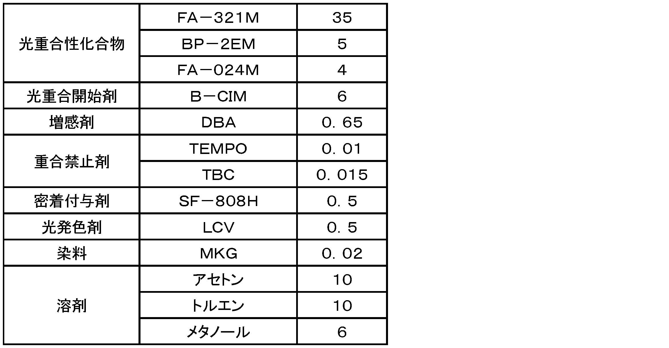
バインダーポリマー溶液の固形分量が56質量部に対して、表2に示す配合量(質量部)の各成分を混合することにより、感光性樹脂組成物を調製した。表2に示す各成分の詳細については、以下のとおりである。
FA-321M:2,2-ビス(4-(メタクリロキシペンタエトキシ)フェニル)プロパン(昭和電工マテリアルズ株式会社製)
BP-2EM:2,2-ビス(4-(メタクリロキシジエトキシ)フェニル)プロパン(共栄社化学株式会社製)
FA-024M:EOPO変性ジメタクリレート(昭和電工マテリアルズ株式会社製)
(光重合開始剤)
B-CIM:2,2’-ビス(2-クロロフェニル)-4,4’,5,5’-テトラフェニルビイミダゾール(Hampford社製)
(増感剤)
DBA:9,10-ジブトキシアントラセン(川崎化成工業株式会社製)
(重合禁止剤)
TEMPO:2,2,6,6-テトラメチルピペリジノオキシルフリーラジカル(株式会社ADEKA製)
TBC:4-tert-ブチルカテコール(DIC株式会社製、商品名「DIC-TBC」)
(密着付与剤)
SF-808H:カルボキシベンゾトリアゾール、5-アミノ-1H-テトラゾール及びメトキシプロパノールの混合物(サンワ化成株式会社製)
(光発色剤)
LCV:ロイコクリスタルバイオレット(山田化学工業株式会社製)
(染料)
MKG:マラカイトグリーン(大阪有機化学工業株式会社製)
支持体として厚さ16μmのポリエチレンテレフタレートフィルム(東レ株式会社製、商品名「QS-69」)を用意した。支持体上に、感光性樹脂組成物を塗布した後、80℃及び120℃の熱風対流式乾燥器で順次乾燥して、乾燥後の厚さが25μmの感光層を形成した。この感光層上に保護層としてポリエチレンフィルム(タマポリ株式会社製、商品名「NF-15」)を貼り合わせ、支持体と感光層と保護層とが順に積層された感光性エレメントを得た。
銅箔(厚さ:35μm)を両面に積層したガラスエポキシ材である銅張積層板(昭和電工マテリアルズ株式会社製、商品名「MCL-E-679」)を、水洗、酸洗及び水洗後、空気流で乾燥した。表面処理された銅張積層板を80℃に加温し、保護層を剥離しながら、感光層が銅表面に接するように、感光性エレメントをラミネートした。これにより、銅張積層板と感光層と支持体とがこの順に積層された積層体を得た。ラミネートは、110℃のヒートロールを用いて、0.4MPaの圧着圧力、1.05m/分のロール速度で行った。
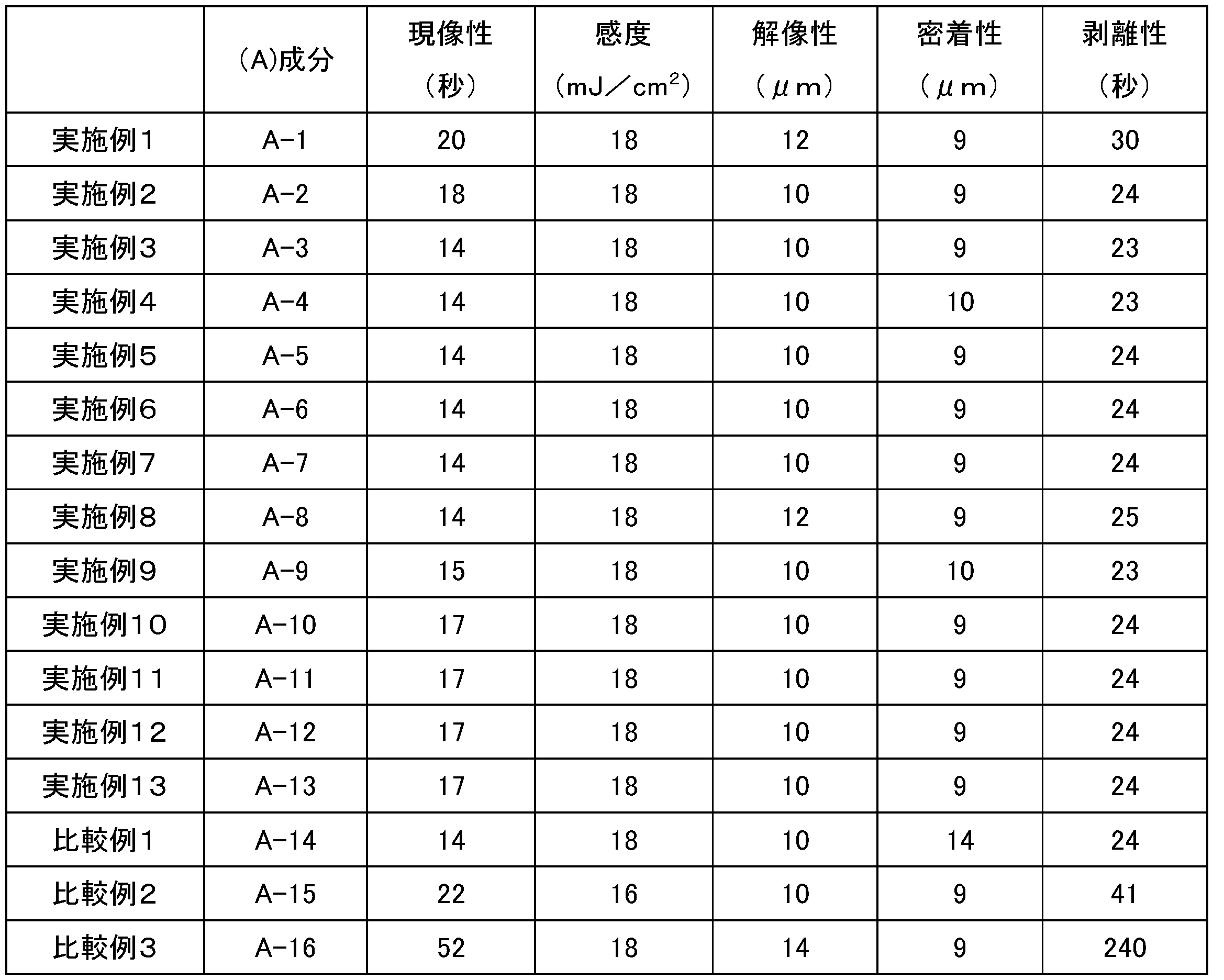
得られた積層体を以下に示す評価の試験片として用いた。評価結果を表3に示す。
上記積層体を5cm四方に切断し、最小現像時間測定用の試験片を得た。試験片から支持体を剥離した後、30℃の1質量%炭酸ナトリウム水溶液を用いて、露光していない感光層を0.15MPaの圧力でスプレー現像し、1mm以上の未露光部が除去されたことを目視で確認できる最短の時間を、最短現像時間とした。ノズルは、フルコーンタイプを使用した。上記試験片とノズル先端との距離は6cmであり、試験片の中心とノズルの中心が一致するように配置した。最小現像時間(単位:秒)が短いほど、現像性が良好であることを意味する。
試験片の支持体上に、日立41段ステップタブレットを載置し、波長405nmの青紫色レーザダイオードを光源とする直描露光機(ビアメカニクス株式会社製、商品名「DE-1UH」)を用いて、日立41段ステップタブレットの現像後の残存ステップ段数が18段となる露光量(照射エネルギー量)で、支持体を介して感光層を露光した。このときの露光量(単位:mJ/cm2)により光感度を評価した。露光量が少ないほど、光感度が高いことを意味する。
ライン幅(L)/スペース幅(S)(以下、「L/S」と記す。)がx/3x(x=1~20(1μm間隔で変化))(単位:μm)である描画パターンを用いて、日立41段ステップタブレットの残存段数が17段となるエネルギー量で、波長405nmの青紫色レーザダイオードを光源とする直描露光機(ビアメカニクス株式会社製、商品名「DE-1UH」)により、上記積層体の感光層に対して露光(描画)を行った。
L/Sがx/x(x=1~20(1μm間隔で変化))(単位:μm)である描画パターンを用いて、日立41段ステップタブレットの残存段数が17段となるエネルギー量で、波長405nmの青紫色レーザダイオードを光源とする直描露光機(ビアメカニクス株式会社製、商品名「DE-1UH」)により、上記積層体の感光層に対して露光(描画)を行った。
前記評価用積層基板上に、剥離性評価用として45mm×65mmの長方形の硬化膜を形成するマスクデータを使用して露光した。次いで上記光感度の評価と同様の条件で現像処理を行って、未露光部を除去した。その後、容量400mLのビーカーに50℃、3.0質量%NaOH水溶液(剥離液)300mLを準備した。剥離液を長さ30mmの攪拌子を用いて200回転/分(rpm)で攪拌しながら、現像後の基板を剥離液に浸漬し、硬化膜が基板から離れるまでの時間を計測した。硬化膜が基板から離れるまでの時間が早いほど、剥離時間が短く剥離性が良好であるといえる。
Claims (16)
- バインダーポリマーと、光重合性化合物と、光重合開始剤と、増感剤と、を含有する感光性樹脂組成物であって、
前記バインダーポリマーが、アクリル酸に由来する構造単位と、スチレン又はスチレン誘導体に由来する構造単位と、脂環構造を有する(メタ)アクリレート化合物に由来する構造単位と、を有するアルカリ可溶性樹脂を含む、感光性樹脂組成物。 - 前記アクリル酸に由来する構造単位の含有量が、前記アルカリ可溶性樹脂を構成する重合性単量体に由来する構造単位の全質量を基準として、15~25質量%である、請求項1に記載の感光性樹脂組成物。
- 前記アルカリ可溶性樹脂の重量平均分子量が、10000~80000である、請求項1又は2に記載の感光性樹脂組成物。
- 前記アルカリ可溶性樹脂の酸価が、140~200mgKOH/gである、請求項1~3のいずれか一項に記載の感光性樹脂組成物。
- 前記増感剤が、アントラセン化合物を含む、請求項1~4のいずれか一項に記載の感光性樹脂組成物。
- 前記光重合性化合物が、オキシエチレン基の数が10以上である2,2-ビス(4-((メタ)アクリロキシポリエトキシ)フェニル)プロパンを含む、請求項1~5のいずれか一項に記載の感光性樹脂組成物。
- 前記光重合性化合物が、オキシエチレン基の数が10未満である2,2-ビス(4-((メタ)アクリロキシポリエトキシ)フェニル)プロパンを含む、請求項1~6のいずれか一項に記載の感光性樹脂組成物。
- 前記光重合性化合物が、オキシエチレン基の数が10以上である2,2-ビス(4-((メタ)アクリロキシポリエトキシ)フェニル)プロパンと、オキシエチレン基の数が10未満である2,2-ビス(4-((メタ)アクリロキシポリエトキシ)フェニル)プロパンとを含む、請求項1~5のいずれか一項に記載の感光性樹脂組成物。
- アクリル酸に由来する構造単位と、スチレン又はスチレン誘導体に由来する構造単位と、脂環構造を有する(メタ)アクリレート化合物に由来する構造単位と、を有する、アルカリ可溶性樹脂。
- 前記アクリル酸に由来する構造単位の含有量が、前記アルカリ可溶性樹脂を構成する重合性単量体に由来する構造単位の全質量を基準として、15~25質量%である、請求項9に記載のアルカリ可溶性樹脂。
- 重量平均分子量が10000~80000である、請求項9又は10に記載のアルカリ可溶性樹脂。
- 酸価が140~200mgKOH/gである、請求項9~11のいずれか一項項に記載のアルカリ可溶性樹脂。
- 支持体と、該支持体上に請求項1~8のいずれか一項に記載の感光性樹脂組成物を用いて形成された感光層と、を備える感光性エレメント。
- 基板上に、請求項1~8のいずれか一項に記載の感光性樹脂組成物又は請求項13に記載の感光性エレメントを用いて、感光層を形成する工程と、
前記感光層の少なくとも一部に活性光線を照射して、光硬化部を形成する工程と、
前記基板から、前記感光層の未光硬化部を除去して、レジストパターンを形成する工程と、
を備える、レジストパターンの形成方法。 - 請求項14に記載のレジストパターンの形成方法によりレジストパターンが形成された基板をエッチング処理又はめっき処理して、導体パターンを形成する工程を備える、プリント配線板の製造方法。
- 前記エッチング処理又はめっき処理の後に、前記レジストパターンを除去する工程を更に備える、請求項15に記載のプリント配線板の製造方法。
Priority Applications (5)
| Application Number | Priority Date | Filing Date | Title |
|---|---|---|---|
| KR1020247041830A KR20250021467A (ko) | 2022-06-08 | 2022-06-08 | 알칼리 가용성 수지, 감광성 수지 조성물, 감광성 엘리먼트, 레지스트 패턴의 형성 방법, 및 프린트 배선판의 제조 방법 |
| JP2024526131A JPWO2023238299A1 (ja) | 2022-06-08 | 2022-06-08 | |
| PCT/JP2022/023189 WO2023238299A1 (ja) | 2022-06-08 | 2022-06-08 | アルカリ可溶性樹脂、感光性樹脂組成物、感光性エレメント、レジストパターンの形成方法、及びプリント配線板の製造方法 |
| CN202280086725.XA CN118475880A (zh) | 2022-06-08 | 2022-06-08 | 碱可溶性树脂、感光性树脂组合物、感光性元件、抗蚀剂图案的形成方法及印刷线路板的制造方法 |
| TW112120665A TW202406943A (zh) | 2022-06-08 | 2023-06-02 | 鹼可溶性樹脂、感光性樹脂組成物、感光性元件、抗蝕劑圖案之形成方法、及印刷線路板之製造方法 |
Applications Claiming Priority (1)
| Application Number | Priority Date | Filing Date | Title |
|---|---|---|---|
| PCT/JP2022/023189 WO2023238299A1 (ja) | 2022-06-08 | 2022-06-08 | アルカリ可溶性樹脂、感光性樹脂組成物、感光性エレメント、レジストパターンの形成方法、及びプリント配線板の製造方法 |
Publications (1)
| Publication Number | Publication Date |
|---|---|
| WO2023238299A1 true WO2023238299A1 (ja) | 2023-12-14 |
Family
ID=89117775
Family Applications (1)
| Application Number | Title | Priority Date | Filing Date |
|---|---|---|---|
| PCT/JP2022/023189 Ceased WO2023238299A1 (ja) | 2022-06-08 | 2022-06-08 | アルカリ可溶性樹脂、感光性樹脂組成物、感光性エレメント、レジストパターンの形成方法、及びプリント配線板の製造方法 |
Country Status (5)
| Country | Link |
|---|---|
| JP (1) | JPWO2023238299A1 (ja) |
| KR (1) | KR20250021467A (ja) |
| CN (1) | CN118475880A (ja) |
| TW (1) | TW202406943A (ja) |
| WO (1) | WO2023238299A1 (ja) |
Families Citing this family (1)
| Publication number | Priority date | Publication date | Assignee | Title |
|---|---|---|---|---|
| CN120040387B (zh) * | 2025-04-23 | 2025-09-09 | 湖南初源新材料股份有限公司 | 一种二环氧烷氧基蒽光敏剂、光固化树脂组合物和感光干膜及应用 |
Citations (2)
| Publication number | Priority date | Publication date | Assignee | Title |
|---|---|---|---|---|
| WO2022030053A1 (ja) * | 2020-08-07 | 2022-02-10 | 昭和電工マテリアルズ株式会社 | 感光性樹脂組成物、感光性エレメント、レジストパターンの形成方法、及びプリント配線板の製造方法 |
| WO2022054599A1 (ja) * | 2020-09-14 | 2022-03-17 | 富士フイルム株式会社 | 感光性転写材料、樹脂パターンの製造方法、エッチング方法、及び、電子デバイスの製造方法 |
Family Cites Families (4)
| Publication number | Priority date | Publication date | Assignee | Title |
|---|---|---|---|---|
| JP2007078889A (ja) * | 2005-09-12 | 2007-03-29 | Fujifilm Corp | 感光性組成物、パターン形成材料、感光性積層体、並びにパターン形成装置及びパターン形成方法 |
| JP4924230B2 (ja) | 2007-06-21 | 2012-04-25 | 日立化成工業株式会社 | 感光性樹脂組成物、これを用いた感光性エレメント、レジストパターンの形成方法及びプリント配線板の製造方法 |
| JP5777461B2 (ja) | 2011-09-14 | 2015-09-09 | 旭化成イーマテリアルズ株式会社 | 感光性樹脂組成物 |
| JP7333735B2 (ja) * | 2019-09-19 | 2023-08-25 | 旭化成株式会社 | 低誘電感光性樹脂組成物、及びその硬化物 |
-
2022
- 2022-06-08 KR KR1020247041830A patent/KR20250021467A/ko active Pending
- 2022-06-08 CN CN202280086725.XA patent/CN118475880A/zh active Pending
- 2022-06-08 JP JP2024526131A patent/JPWO2023238299A1/ja active Pending
- 2022-06-08 WO PCT/JP2022/023189 patent/WO2023238299A1/ja not_active Ceased
-
2023
- 2023-06-02 TW TW112120665A patent/TW202406943A/zh unknown
Patent Citations (2)
| Publication number | Priority date | Publication date | Assignee | Title |
|---|---|---|---|---|
| WO2022030053A1 (ja) * | 2020-08-07 | 2022-02-10 | 昭和電工マテリアルズ株式会社 | 感光性樹脂組成物、感光性エレメント、レジストパターンの形成方法、及びプリント配線板の製造方法 |
| WO2022054599A1 (ja) * | 2020-09-14 | 2022-03-17 | 富士フイルム株式会社 | 感光性転写材料、樹脂パターンの製造方法、エッチング方法、及び、電子デバイスの製造方法 |
Also Published As
| Publication number | Publication date |
|---|---|
| KR20250021467A (ko) | 2025-02-13 |
| TW202406943A (zh) | 2024-02-16 |
| JPWO2023238299A1 (ja) | 2023-12-14 |
| CN118475880A (zh) | 2024-08-09 |
Similar Documents
| Publication | Publication Date | Title |
|---|---|---|
| JP5327310B2 (ja) | 感光性樹脂組成物、並びにこれを用いた感光性エレメント、レジストパターンの形成方法及びプリント配線板の製造方法 | |
| JPWO2010098175A1 (ja) | 感光性樹脂組成物、並びにこれを用いた感光性エレメント、レジストパターンの形成方法及びプリント配線板の製造方法 | |
| WO2024210041A1 (ja) | 感光性樹脂組成物、感光性エレメント、レジストパターンの形成方法及び配線基板の製造方法 | |
| TW202406943A (zh) | 鹼可溶性樹脂、感光性樹脂組成物、感光性元件、抗蝕劑圖案之形成方法、及印刷線路板之製造方法 | |
| JP2024526665A (ja) | 感光性組成物、感光性エレメント、及び配線基板の製造方法 | |
| JP2010085605A (ja) | 感光性樹脂組成物、これを用いた感光性エレメント、レジストパターンの形成方法及びプリント配線板の製造方法 | |
| JP7856211B2 (ja) | 感光性樹脂組成物、感光性エレメント、硬化物、レジストパターンの形成方法、及び、プリント配線板の製造方法 | |
| EP4692936A1 (en) | Photosensitive resin composition, photosensitive element, method for forming resist pattern, and method for producing printed wiring board | |
| JP7816574B2 (ja) | 感光性樹脂組成物、感光性エレメント、及び配線基板の製造方法 | |
| WO2025115821A1 (ja) | 感光性樹脂組成物、感光性エレメント、レジストパターンの形成方法及びプリント配線板の製造方法 | |
| WO2025126273A1 (ja) | 感光性樹脂組成物、感光性エレメント、レジストパターンの形成方法及びプリント配線板の製造方法 | |
| WO2025070065A1 (ja) | 感光性樹脂組成物、感光性エレメント、レジストパターンの形成方法、及び配線基板の製造方法 | |
| WO2024135574A1 (ja) | 感光性樹脂組成物、感光性エレメント、レジストパターンの形成方法、及びプリント配線板の製造方法 | |
| WO2024134889A1 (ja) | 感光性樹脂組成物、感光性エレメント、レジストパターンの形成方法、及びプリント配線板の製造方法 | |
| WO2024142486A1 (ja) | 感光性エレメント及び配線基板の製造方法 | |
| WO2025074828A1 (ja) | 感光性樹脂組成物、感光性エレメント、レジストパターンの形成方法、及びプリント配線板の製造方法 | |
| WO2025094282A1 (ja) | 感光性エレメント、レジストパターンの形成方法、及びプリント配線板の製造方法 | |
| WO2025220085A1 (ja) | 感光性エレメント、レジストパターンの形成方法、及び配線基板の製造方法 | |
| WO2026022983A1 (ja) | 感光性エレメント、レジストパターンの形成方法、及びプリント配線板の製造方法 | |
| WO2024195502A1 (ja) | 感光性樹脂組成物、感光性エレメント、レジストパターンの形成方法及び配線基板の製造方法 | |
| WO2026042763A1 (ja) | 感光性エレメント、レジストパターンの形成方法、及びプリント配線板の製造方法 |
Legal Events
| Date | Code | Title | Description |
|---|---|---|---|
| 121 | Ep: the epo has been informed by wipo that ep was designated in this application |
Ref document number: 22945802 Country of ref document: EP Kind code of ref document: A1 |
|
| WWE | Wipo information: entry into national phase |
Ref document number: 2024526131 Country of ref document: JP |
|
| WWE | Wipo information: entry into national phase |
Ref document number: 202280086725.X Country of ref document: CN |
|
| ENP | Entry into the national phase |
Ref document number: 20247041830 Country of ref document: KR Kind code of ref document: A |
|
| NENP | Non-entry into the national phase |
Ref country code: DE |
|
| WWP | Wipo information: published in national office |
Ref document number: 1020247041830 Country of ref document: KR |
|
| 122 | Ep: pct application non-entry in european phase |
Ref document number: 22945802 Country of ref document: EP Kind code of ref document: A1 |