WO2023233921A1 - 電磁波反射装置、電磁波反射フェンス、及び反射パネル - Google Patents
電磁波反射装置、電磁波反射フェンス、及び反射パネル Download PDFInfo
- Publication number
- WO2023233921A1 WO2023233921A1 PCT/JP2023/017231 JP2023017231W WO2023233921A1 WO 2023233921 A1 WO2023233921 A1 WO 2023233921A1 JP 2023017231 W JP2023017231 W JP 2023017231W WO 2023233921 A1 WO2023233921 A1 WO 2023233921A1
- Authority
- WO
- WIPO (PCT)
- Prior art keywords
- electromagnetic wave
- conductive pattern
- layer
- adhesive layer
- dielectric layer
- Prior art date
- Legal status (The legal status is an assumption and is not a legal conclusion. Google has not performed a legal analysis and makes no representation as to the accuracy of the status listed.)
- Ceased
Links
Images





Classifications
-
- H—ELECTRICITY
- H01—ELECTRIC ELEMENTS
- H01Q—ANTENNAS, i.e. RADIO AERIALS
- H01Q15/00—Devices for reflection, refraction, diffraction or polarisation of waves radiated from an antenna, e.g. quasi-optical devices
- H01Q15/14—Reflecting surfaces; Equivalent structures
Definitions
- the present invention relates to an electromagnetic wave reflecting device, an electromagnetic wave reflecting fence, and a reflecting panel.
- 5G 5th generation
- NLOS Non-Line-Of-Sight
- a metasurface is formed of a periodic structure or pattern that is finer than a wavelength, and is designed to reflect radio waves in a desired direction (see, for example, Non-Patent Document 1).
- the metasurface itself is realized by periodically repeating minute structures or metal patterns, but when actually manufactured, a metal pattern is provided on one side of a dielectric substrate, and a metal pattern is placed on the opposite side.
- a ground layer is often provided. Since metasurfaces can achieve a desired reflection angle while maintaining a planar arrangement, they function effectively as reflectors even in environments where there is not enough space to install a large number of electromagnetic wave reflecting panels.
- Metal patterns and ground layers are often formed of metals with good conductivity such as copper (Cu), nickel (Ni), and silver (Ag). Reflective surfaces, including metasurfaces, function with metal patterns and require precise patterning.
- the ground layer is formed on one surface of the dielectric substrate by a process such as sputtering or vapor deposition.
- the metal pattern may be formed by etching, electrolytic plating, or the like.
- an electromagnetic wave reflecting panel of a desired size by tiling a plurality of adhesive layers each having a metal pattern formed in a certain size area on a dielectric layer.
- the dielectric constants of the dielectric substrate and adhesive layer have a large effect on the reflection angle and reflection efficiency.
- the reflection efficiency is 60% or more, or 70% or more. Therefore, there is a need for a configuration that can suppress a decrease in reflection efficiency when bonding a plurality of adhesive films carrying metal patterns to a dielectric substrate.
- One object of the present invention is to provide an electromagnetic wave reflecting device that suppresses a decrease in reflection efficiency and has a desired size.
- the electromagnetic wave reflecting device includes a reflective panel that reflects radio waves in a desired band selected from a frequency band of 1 GHz or more and 170 GHz or less, and a frame that holds the reflective panel,
- the reflective panel includes a dielectric layer, a periodic conductive pattern provided on one surface of the dielectric layer, a ground layer provided on the other surface of the dielectric layer, and a ground layer that connects the conductive pattern to the dielectric layer.
- an adhesive layer bonded to the one surface of the layer A plurality of the adhesive layers carrying the conductive patterns are tiled on the one surface of the dielectric layer in a first direction or in a second direction perpendicular to the first direction.
- FIG. 2 is a schematic diagram of an electromagnetic wave reflecting fence in which a plurality of electromagnetic wave reflecting devices are connected.
- FIG. 3 is a diagram showing an example of application of an electromagnetic wave reflecting fence to a process line. 2 is a horizontal cross-sectional view of the frame taken along line AA in FIG. 1.
- FIG. 3 is a diagram showing a state in which a panel is inserted into the frame of FIG. 2.
- FIG. It is a figure showing an example of the layer composition of a reflective panel. It is a figure which shows another example of the layer structure of a reflective panel.
- FIG. 3 is a diagram showing a model of a conductive pattern used for evaluating reflection characteristics.
- FIG. 3 is a diagram showing an example of the basic structure of an adhesive layer supporting unit cells.
- FIG. 7 is a diagram showing an example of tiling of the basic structure of FIG. 6.
- FIG. FIG. 3 is a diagram showing an analysis space. It is a schematic diagram of the XY plane of analysis space. It is a schematic diagram of the XZ plane of analysis space. It is a schematic diagram of the YZ plane of analysis space.
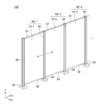
- FIG. 1A is a schematic diagram of an electromagnetic wave reflecting fence 100 in which electromagnetic wave reflecting devices 60-1, 60-2, and 60-3 are connected.
- an electromagnetic wave reflecting fence 100 is configured by connecting three electromagnetic wave reflecting devices 60-1, 60-2, and 60-3 (hereinafter may be collectively referred to as "electromagnetic wave reflecting device 60" as appropriate).
- electromagnettic wave reflecting device 60 there is no particular limit to the number of electromagnetic wave reflecting devices 60 that are connected.
- the electromagnetic wave reflecting devices 60-1, 60-2, and 60-3 each have reflective panels 10-1, 10-2, and 10-3 (hereinafter, may be collectively referred to as "reflective panels 10" as appropriate).
- the width direction of the reflective panel 10 is the X direction
- the height direction is the Y direction
- the thickness direction is the Z direction.
- Each reflective panel 10 reflects electromagnetic waves of 1 GHz or more and 170 GHz or less, preferably 1 GHz or more and 100 GHz or less, and more preferably 1 GHz or more and 80 GHz or less.
- Each reflective panel 10 has a conductive pattern or a conductive film designed according to the intended reflection mode, frequency band, etc. as a reflective film.
- the reflective panels 10-1, 10-2, and 10-3 may be electrically connected to each other from the viewpoint of maintaining continuity of reflected potential, but if they include a metasurface, adjacent reflective panels There may be no electrical connection between panels 10.
- an electromagnetic wave reflective fence 100 connected in the X direction is obtained.
- the electromagnetic wave reflecting device 60 may have legs 56 that support the frame 50. As shown in FIG. 1A, when the electromagnetic wave reflecting device 60 or the electromagnetic wave reflecting fence 100 is made to stand up on an installation surface, it is desirable to provide the legs 56, but the legs 56 are not essential.
- a top frame 57 that holds the upper end of the reflective panel 10 and a bottom frame 58 that holds the lower end may be used.
- the frame 50, the top frame 57, and the bottom frame 58 constitute a frame that holds the entire circumference of the reflective panel 10.
- the frame 50 may also be called a "side frame" due to its positional relationship with the top frame 57 and bottom frame 58.
- the electromagnetic wave reflecting device 60 may be installed on a wall or ceiling while the reflective panel 10 is held by the frame 50, top frame 57, and bottom frame 58.
- FIG. 1B shows an example of application of the electromagnetic wave reflecting fence 100 of FIG. 1A to a process line P.
- a base station BS is placed near a process line P in a factory, production facility, or the like.
- the base station BS transmits and receives radio waves included in a band of 1 GHz or more and 170 GHz or less.
- production equipment M that transmits and receives radio waves to and from the base station BS is arranged.
- FIG. 1B shows one production equipment M in FIG. 1B for convenience of illustration, a large number of production equipment M and structures exist inside the actual process line P.
- the electromagnetic wave reflecting device 60 or the electromagnetic wave reflecting fence 100 is arranged along the long side of the process line P, for example, to improve the propagation environment of the process line P.
- the width A and length B of the process line P vary depending on the environment in which it is installed.
- the size required for the reflecting surface of the electromagnetic wave reflecting device 60 changes depending on the length of the assumed process line. For example, when a 30 m process line is assumed, it is desirable to be able to cover a Fresnel zone radius of 0.5 m or more, and when a 50 m or more process line is assumed, it is desirable to be able to cover a Fresnel zone radius of at least 0.7 m or more.
- FIG. 2 shows an example of the configuration of the frame 50 along line AA in FIG. 1A in a cross-sectional view parallel to the XZ plane.
- the frame 50 has a conductive main body 500 and slits 51 formed on both sides of the main body 500 in the width direction.
- the slits 51 hold the side edges of the reflective panel 10.
- the side edge of the reflective panel 10 is an edge along the Y direction in FIG. 1A.
- the main body 500 is formed with a cavity 52 that communicates with the slit 51, a groove 53 provided in the cavity 52, and a hollow 55 that does not communicate with the cavity 52 and the groove 53, but is not limited to this example.
- the groove 53 is provided at a position facing the slit 51 with the cavity 52 in between, and holds the side edge of the reflective panel 10 inserted through the slit 51. By providing the cavity 52 and the hollow 55 in the frame 50, the weight of the frame 50 can be reduced. By providing the groove 53 in the cavity 52, the reflective panel 10 can be held firmly.
- a non-conductive cover 501 made of resin or the like may be provided on the outer surface of the main body 500, but the cover 501 is not essential. When the cover 501 is provided, the cover 501 functions as a protection member that protects the frame 50.
- FIG. 3 shows a state in which the reflective panel 10 is inserted into the frame 50 in a cross-sectional view parallel to the XZ plane.
- the reflective panels 10-1 and 10-2 are inserted through the slits 51 (see FIG. 2) on both sides of the main body 500.
- the reflective panels 10-1 and 10-2 may or may not necessarily be inserted all the way into the groove 53 (see FIG. 2) of the cavity 52 and come into contact with the bottom surface of the groove 53.
- a portion of body 500 may be formed of a non-conductive material.
- the dielectric layer 14 is an insulating polymer film made of polycarbonate, cycloolefin polymer (COP), polyethylene terephthalate (PET), fluororesin, etc., and has a thickness of about 0.3 mm to 1.0 mm.
- the dielectric layer 14 may be any material as long as it has a relative dielectric constant and a dielectric loss tangent suitable for realizing the target reflection characteristics.
- the conductive pattern 151 forms a reflective surface of the reflective panel 10.
- the reflective surface formed by the conductive pattern 151 may include a metasurface whose reflective properties are artificially controlled.
- the conductive pattern 151 of the embodiment has a periodic pattern and forms a non-specular reflective surface that reflects incident electromagnetic waves in a direction different from the incident angle.
- the conductive pattern 151 is made of a good conductor such as Cu, Ni, or Ag, and has a thickness of 0.01 mm or more and 0.05 mm or less.
- the plurality of adhesive layers 153 are tiled on the surface of the dielectric layer 14 at predetermined intervals to suppress a decrease in the reflection efficiency of the reflective panel 10.
- a material such as vinyl acetate resin, acrylic resin, cellulose resin, aniline resin, ethylene resin, silicone resin, or other resin having a composition satisfying a predetermined dielectric constant and dielectric loss tangent can be used.
- the thickness of the adhesive layer 153 is 0.002 mm or more and 0.05 mm or less, and from the viewpoint of stably holding the conductive pattern 151, it is preferably 0.01 mm or more and 0.05 mm or less.
- the reflective panel 10B includes, in addition to the configuration of FIG. 4A, an intermediate layer 16 that covers the conductive pattern 151, a dielectric substrate 17 joined to the conductive pattern 151 side by the intermediate layer 16, and a ground layer 13. It has a covering intermediate layer 12 and a dielectric substrate 11 connected to the ground layer 13 side by the intermediate layer 12.
- the intermediate layer 16 protects the surface of the conductive pattern 151 and also adheres and holds the dielectric substrate 17.
- the intermediate layer 16 desirably has durability and moisture resistance, and can be made of, for example, ethylene-vinyl acetate (EVA) copolymer or cycloolefin polymer (COP).
- EVA ethylene-vinyl acetate
- COP cycloolefin polymer
- the thickness of the intermediate layer 16 is 0.01 mm or more and 0.40 mm or less.
- the dielectric substrate 17 is desirably formed of a material with excellent impact resistance, durability, and transparency as the outermost layer of the reflective panel 10C.
- the dielectric substrate 17 polycarbonate, acrylic resin, PET, etc. can be used.
- the thickness of the dielectric substrate 17 is, for example, 1.0 mm to 10.0 mm.
- the intermediate layer 12 protects the surface of the ground layer 13 and also adheres and holds the dielectric substrate 11.
- the intermediate layer 12 desirably has durability and moisture resistance, and can be made of, for example, ethylene-vinyl acetate (EVA) copolymer or cycloolefin polymer (COP).
- EVA ethylene-vinyl acetate
- COP cycloolefin polymer
- the thickness of the intermediate layer 12 is 0.01 mm or more and 0.40 mm or less.
- the dielectric substrate 11 is desirably formed of a material with excellent impact resistance, durability, and transparency as the outermost layer of the reflective panel 10C.
- the dielectric substrate 11 polycarbonate, acrylic resin, PET, etc. can be used.
- the thickness of the dielectric substrate 11 is, for example, 1.0 mm to 10.0 mm.
- the conductive pattern 151 By covering the conductive pattern 151 with the intermediate layer 16 and bonding the dielectric substrate 17, moisture and air are prevented from entering the surface of the conductive pattern 151, and deterioration of the reflective surface is suppressed.
- the ground layer 13 By covering the ground layer 13 with the intermediate layer 12 and bonding the dielectric substrate 11, moisture and air are prevented from entering the surface of the ground layer 13, and surface deterioration of the ground layer 13 is suppressed. Thereby, the capacitance between the ground layer 13 and the conductive pattern 151 is maintained constant, and the designed magnitude of the phase delay can be maintained. That is, it is possible to maintain the reflection efficiency of radio waves in the designed direction.
- the arrangement of the adhesive layer 153 supporting the conductive pattern 151 is optimized.
- the spacing between the adhesive layers 153 tiled on the dielectric layer 14 within a predetermined range, a decrease in reflection efficiency is suppressed.
- an appropriate distance between adhesive layers 153 adjacent to each other in the X direction and the Y direction on the dielectric layer 14 will be considered.
- FIG. 5 shows a model 21 of the conductive pattern 151 used for evaluating the reflective panel 10.
- the model 21 for evaluation includes a periodic array of unit cells (also called "supercells") 210. By repeatedly arranging unit cells 210 formed of predetermined conductive patterns 151 in the X and Y directions, a metasurface that reflects electromagnetic waves at an angle different from the incident angle is formed.
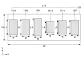
- FIG. 6 shows an example of an adhesive layer 153 carrying a single unit cell 210.
- the unit cell 210 is formed of six conductive patterns 151a, 151b, 151c, 151d, 151e, and 151f.
- the width (W) direction and length (L) direction of the conductive patterns 151a-151f correspond to the width (X) direction and height (Y) direction of the reflective panel 10 in FIG. 1A, respectively.
- the conductive patterns 151a-151f have the same width W.
- the lengths L1 to L6 of the conductive patterns 151a to 151f are different, the central axes of the lengths are aligned (the Y coordinate position of the central axes is constant).
- the pitch in the X direction is constant.
- the unit cell 210 includes an array of conductive patterns 151a-151 provided periodically in the X direction.
- the phase of reflection is controlled by the shape and size of the conductive patterns 151a-151f, and a reflected beam is formed in a desired direction by superimposing the reflected waves.
- the unit cell 210 is designed so that the peak of the reflected wave of the vertically incident electromagnetic wave (incident angle of 0°) appears in the direction of 50° from the normal.
- the unit cell 210 is supported on an adhesive layer 153 of a predetermined size.
- a configuration in which a single unit cell 210 is provided on the adhesive layer 153 is referred to as a "basic configuration.”
- FIG. 7 shows an example of tiling of the adhesive layer 153 in the basic configuration of FIG. 6.
- a plurality of adhesive layers 153 are arranged in the X direction and the Y direction.
- a total of four adhesive layers 153 are arranged, two each in the X direction and the Y direction.
- Three or more adhesive layers 153 may be arranged.
- Gx be the distance between adjacent adhesive layers 153 in the X direction
- Gy be the distance between adjacent adhesive layers 153 in the Y direction. Reflection efficiency is calculated and evaluated while changing the distances Gx and Gy.
- a 28.0 GHz plane wave is incident at an incident angle of 0° using general-purpose three-dimensional electromagnetic field simulation software, and the scattering cross section of the reflected wave is analyzed.
- the scattering cross section, or radar cross section (RCS) is used as an indicator of the ability to reflect incident electromagnetic waves.
- the power reflection efficiency of the metasurface is a value obtained by dividing the power reflection efficiency obtained from the gain value by the correction value.
- E MR be the reflected electric field on the lossless metasurface determined by the model pattern in Figure 5
- E PEC be the reflected electric field on the ideal conductive plate
- ⁇ is the angle of incidence on the metasurface
- ⁇ is the corresponding angle of reflection for regular reflection.
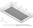
- FIG. 8 shows an analysis space 101 for electromagnetic wave simulation. Assuming that the thickness direction of the layered structure of the reflective panel 10 is the Z direction, the width direction of the metal patch of the model 21 in FIG. size) x (size in Z direction). The size of the analysis space 101 when the frequency of the incident electromagnetic wave is 28.0 GHz is 83.9 mm x 192.6 mm x 3.7 mm. The boundary condition is a design in which electromagnetic wave absorbers 102 are arranged around the analysis space 101.
- Example 1 As the dielectric layer 14, a polycarbonate film with a thickness of 0.7 mm is used. A ground layer 13 made of an Ag-based multilayer film with a thickness of 0.36 mm is set on one side of the polycarbonate film. On the other side of the polycarbonate film, a plurality of basic structures each having an adhesive layer 153 with dimensions X0 ⁇ Y0 (ie, 13.97 mm ⁇ 5.35 mm) on which conductive patterns 151a to 151f are formed are arranged. The conductive patterns 151a-151f are made of copper foil with a thickness of 0.03 mm.
- the conductive patterns 151a to 151f have a rectangular shape with a width W of uniformly 1.5 mm, and have periodicity in the X direction.
- the distance between the conductive patterns 151 in the X direction that is, the gap between the patterns, is uniformly 0.8283 mm.
- the lengths L1-L6 of the conductive patterns 151a-151f are 2.468 mm, 2.796 mm, 3.091 mm, 0.903 mm, 1.225 mm, and 2.359 mm, respectively.
- the occupancy rate of the conductive patterns 151a-151f with respect to the adhesive layer 153 is 35.8%.
- the distance in the X direction of 0.87 mm corresponds to 6.25% of X0 (13.97 mm).
- the gain value at 50° of the RCS plot that is, the peak value of the reflected waveform is 10.5262 dB.
- a power reflection efficiency of 60% or more can be obtained.
- Example 2 In Example 2, the conditions are the same as in Example 1 except for the distance between adjacent adhesive layers 153.
- the distance between the adhesive layers 153 in the Y direction of 1.34 mm corresponds to 25.00% of Y0 (5.35 mm).
- the gain value at 50° of the RCS plot that is, the peak value of the reflected waveform is 10.6322 dB.
- a power reflection efficiency of 60% or more can be obtained.
- Example 3 In Example 3, the conditions are the same as in Example 1 except for the distance between adjacent adhesive layers 153.
- the distance between the adhesive layers 153 in the Y direction of 2.68 mm corresponds to 50.00% of Y0 (5.35 mm).
- the gain value at 50° of the RCS plot that is, the peak value of the reflected waveform is 10.6327 dB.
- a power reflection efficiency of 60% or more can be obtained.
- Example 5 In Example 5, the conditions are the same as in Example 1 except for the distance between adjacent adhesive layers 153.
- the gain value at 50° of the RCS plot that is, the peak value of the reflected waveform is 10.6654 dB.
- a power reflection efficiency of 60% or more can be obtained.
- the occupancy rate of the conductive pattern 151 formed on the adhesive layer 153 is changed.
- the conditions for the dielectric layer 14, ground layer 13, and adhesive layer 153 are the same as in Example 1-5.
- Rectangular conductive patterns 151a to 151f with a uniform width of 0.7 mm are provided on the adhesive layer 153 with X0 ⁇ Y0 of 13.97 mm ⁇ 5.35 mm.
- Lengths L1-L6 of conductive patterns 151a-151f are the same as in Embodiment 1-5, and are 2.468 mm, 2.796 mm, 3.091 mm, 0.903 mm, 1.225 mm, and 2.359 mm, respectively.
- the pitch (distance between centers) of the conductive patterns 151 in the X direction is uniformly 2.329 mm. At this time, the occupation rate of the conductive patterns 151a to 151f with respect to the adhesive layer 153 is 11.5%.
- the gain value at 50° of the RCS plot that is, the peak value of the reflected waveform is 11.4780 dB.
- a power reflection efficiency of 70% or more can be obtained.
- Example 7 In the seventh embodiment, the same conditions as in the sixth embodiment are used except for the thickness of the conductive pattern 151.
- Conductive patterns 151a to 151f having the same planar shape as in Example 6 and having a thickness of 0.05 mm are provided on the adhesive layer 153 with X0 ⁇ Y0 of 13.97 mm ⁇ 5.35 mm.
- the occupancy rate of the conductive patterns 151a-151f with respect to the adhesive layer 153 is 11.5%.
- Comparative Example 1 In Comparative Example 1, the same conditions as in Example 1 were used except for the distance between adjacent adhesive layers 153.
- the interval in the X direction of the adhesive layer 153 was set to 12.50% of X0, which caused the period in the X direction to be disturbed, and it is considered that the reflection efficiency in the designed direction deteriorated.
- Comparative Example 3 In Comparative Example 3, the same conditions as in Example 1 were used except for the distance between adjacent adhesive layers 153.
- the gain value at 50° in the RCS plot that is, the peak value of the reflected waveform is ⁇ 12.0314 dB.
- the unit cells 210 are far apart in the X direction and do not function as an electromagnetic wave reflecting panel.
- Comparative Example 4 In Comparative Example 4, the same conditions as in Example 1 were used except for the distance between adjacent adhesive layers 153.
- Comparative Example 4 it is considered that the reflection efficiency in the designed direction deteriorated because the intervals between the unit cells 210 were greatly separated in the Y direction.
- the adhesive layer 153 when a plurality of adhesive layers 153 of the basic configuration supporting a single unit cell 210 are tiled on the dielectric layer 14
- the interval is as follows. (a) When the conductive pattern 151 provided on the adhesive layer 153 has periodicity in the X direction, the interval Gx in the X direction between adjacent adhesive layers 153 is 0 of the length X0 in the X direction of the adhesive layer in the basic configuration. .0% or more and 10.0% or less.
- the interval Gy between adjacent adhesive layers 153 in the Y direction is 0 of the length Y0 of the adhesive layer in the basic configuration in the Y direction. .0% or more and 100.0% or less.
- the thickness of the conductive pattern is changed in the range of 0.01 mm or more and 0.05 mm or less, it hardly affects the calculation result of the power reflection efficiency, but the occupancy rate of the conductive pattern 151 with respect to the adhesive layer 153 or the dielectric layer 14 affects the power reflection efficiency.
- Changing the tiling interval of the adhesive layer 153 that carries a certain conductive pattern 151 is equivalent to changing the occupancy rate of the conductive pattern 151 with respect to the dielectric layer 14.
- changing the line width of the conductive pattern 151 provided on the adhesive layer 153 having the basic structure of tiling without gaps is equivalent to changing the occupation rate of the conductive pattern 151 with respect to the dielectric layer.
- the transmittance of visible light can be maintained at a certain level or more, and the reflection efficiency can be maintained at a certain level or higher. can be increased to 60% or more. Therefore, so that the occupancy rate of the conductive pattern 151 with respect to the dielectric layer 14 is 10% or more and 45% or less, the distance Gx between adjacent adhesive layers 153 in the X direction is set to 0.0% or more and 10.0% or less of X0.
- the interval Gy in the Y direction may be adjusted within the range of 0.0% or more and 100.0% or less of Y0.
- the power reflection efficiency can be improved to 80% or more by increasing the occupancy of the conductive pattern 151 to 45% or more.
- the power reflection efficiency is as follows: This is equivalent to the power reflection efficiency when the cell 210 is formed. Therefore, even when the adhesive layer 153 having an expanded configuration in which a large number of unit cells 210 are provided on the adhesive layer 153 having a fixed area is arranged at intervals within the above-mentioned range, a reflection efficiency of 60% or more can be obtained.
- the reflecting surface of the electromagnetic wave reflecting device 60 provided along the process line P in FIG. You may also tile four adhesive sheets provided with . This is because if the area is approximately 35 cm x 35 cm, the conductive pattern 151 including a large number of unit cells 210 can be produced all at once without difficulty.
- the spacing in the X and Y directions when tiling the adhesive layer 153 in the expanded configuration including a large number of unit cells 210 is the same as in the tiling of the adhesive layer in the basic configuration. If the length of the adhesive layer in the basic configuration including a single unit cell 210 in the X direction is X0 and the length in the Y direction is Y0, then the interval in the X direction of the adhesive layer 153 in the expanded configuration is 0.0% of X0. The above is 10.0% or less, and the interval in the Y direction is 0.0% or more and 100.0% or less of Y0.
- the size of the reflective panel of the electromagnetic wave reflective fence 100 in FIG. May be tiled.
- a 250 mm x 300 mm or 250 mm x 150 mm adhesive layer 153 having a large number of unit cells formed thereon may be tiled on the dielectric layer 14 .
- both reflectance and transmittance can be achieved by setting the occupancy rate of the conductive pattern 151 to the dielectric layer 14 to 10% or more and 45%. can.
- a reflective panel 10 with a reflection efficiency of 60% or more can be realized in a desired size.
- the adhesive layer 153 may be tiled only in either the X direction or the Y direction, or may be tiled in both directions. This expands the scope of application of the electromagnetic wave reflecting device 60, and also suppresses increases in manufacturing costs.
- Electromagnetic wave reflecting device 100
- Electromagnetic wave reflecting fence 210 Unit cell Gx Space between adhesive layers in the X direction Gy Space between adhesive layers in the Y direction X0 Adhesion of basic configuration Length of the layer in the X direction Y0 Length of the adhesive layer in the basic configuration in the Y direction
Landscapes
- Physics & Mathematics (AREA)
- Electromagnetism (AREA)
- Aerials With Secondary Devices (AREA)
Priority Applications (1)
| Application Number | Priority Date | Filing Date | Title |
|---|---|---|---|
| JP2024524270A JPWO2023233921A1 (https=) | 2022-06-01 | 2023-05-08 |
Applications Claiming Priority (2)
| Application Number | Priority Date | Filing Date | Title |
|---|---|---|---|
| JP2022-089851 | 2022-06-01 | ||
| JP2022089851 | 2022-06-01 |
Publications (1)
| Publication Number | Publication Date |
|---|---|
| WO2023233921A1 true WO2023233921A1 (ja) | 2023-12-07 |
Family
ID=89026317
Family Applications (1)
| Application Number | Title | Priority Date | Filing Date |
|---|---|---|---|
| PCT/JP2023/017231 Ceased WO2023233921A1 (ja) | 2022-06-01 | 2023-05-08 | 電磁波反射装置、電磁波反射フェンス、及び反射パネル |
Country Status (2)
| Country | Link |
|---|---|
| JP (1) | JPWO2023233921A1 (https=) |
| WO (1) | WO2023233921A1 (https=) |
Citations (4)
| Publication number | Priority date | Publication date | Assignee | Title |
|---|---|---|---|---|
| JP2018110193A (ja) * | 2017-01-05 | 2018-07-12 | 住友電工プリントサーキット株式会社 | プリント配線用原板及びプリント配線板 |
| WO2021199504A1 (ja) * | 2020-03-31 | 2021-10-07 | Agc株式会社 | 無線伝達システム |
| WO2022070901A1 (ja) * | 2020-09-29 | 2022-04-07 | 日東電工株式会社 | ミリ波アンテナ |
| JP2022072812A (ja) * | 2020-10-30 | 2022-05-17 | 電気興業株式会社 | 可変リフレクトアレーおよび可変リフレクトアレーの設計方法 |
-
2023
- 2023-05-08 JP JP2024524270A patent/JPWO2023233921A1/ja active Pending
- 2023-05-08 WO PCT/JP2023/017231 patent/WO2023233921A1/ja not_active Ceased
Patent Citations (4)
| Publication number | Priority date | Publication date | Assignee | Title |
|---|---|---|---|---|
| JP2018110193A (ja) * | 2017-01-05 | 2018-07-12 | 住友電工プリントサーキット株式会社 | プリント配線用原板及びプリント配線板 |
| WO2021199504A1 (ja) * | 2020-03-31 | 2021-10-07 | Agc株式会社 | 無線伝達システム |
| WO2022070901A1 (ja) * | 2020-09-29 | 2022-04-07 | 日東電工株式会社 | ミリ波アンテナ |
| JP2022072812A (ja) * | 2020-10-30 | 2022-05-17 | 電気興業株式会社 | 可変リフレクトアレーおよび可変リフレクトアレーの設計方法 |
Also Published As
| Publication number | Publication date |
|---|---|
| JPWO2023233921A1 (https=) | 2023-12-07 |
Similar Documents
| Publication | Publication Date | Title |
|---|---|---|
| US12261367B2 (en) | Antenna unit and window glass | |
| US20250055201A1 (en) | Electromagnetic wave reflecting device, electromagnetic wave reflecting fence, and reflection panel | |
| US20220416414A1 (en) | Antenna unit and window glass | |
| US20250174903A1 (en) | Frequency-selective reflecting plate and communication relay system | |
| US20250096480A1 (en) | Electromagnetic wave reflecting device, electromagnetic wave reflecting fence, and reflection panel | |
| US20230402750A1 (en) | Reflectarray and method therefor | |
| WO2024127942A1 (ja) | 無線伝達システム | |
| KR20250006862A (ko) | 전자파 반사 장치 및 전자파 반사 펜스 | |
| EP1900114A1 (en) | A passive repeater antenna | |
| WO2024029325A1 (ja) | 反射パネル、これを用いた電磁波反射装置、及び電磁波反射フェンス | |
| WO2023233921A1 (ja) | 電磁波反射装置、電磁波反射フェンス、及び反射パネル | |
| WO2023233885A1 (ja) | 電磁波反射装置、電磁波反射フェンス、及び反射パネル | |
| WO2025158773A1 (ja) | 電磁波反射パネル、電磁波反射装置、及び電磁波反射フェンス | |
| WO2024029365A1 (ja) | 反射パネル、これを用いた電磁波反射装置、及び電磁波反射フェンス | |
| CN120752812A (zh) | 反射阵列、反射阵列装置以及反射阵列的设计方法 | |
| WO2024241665A1 (ja) | 電磁波反射パネル、電磁波反射装置、及び電磁波反射フェンス | |
| EP4243199A1 (en) | Antenna set | |
| US20250309555A1 (en) | Reflection panel and electromagnetic-wave reflecting apparatus | |
| CN114566811A (zh) | 一种模块化可拼接高环境适应性天线子阵 | |
| WO2024135216A1 (ja) | 反射パネル、電磁波反射装置、及び電磁波反射フェンス | |
| JP7715266B2 (ja) | リフレクトアレイ、電磁波反射システムおよびリフレクトアレイの設置方法 | |
| WO2024185325A1 (ja) | 電磁波反射パネルの製造方法 | |
| JP2026054790A (ja) | 電波反射体および反射鏡アンテナ | |
| WO2024247411A1 (ja) | 電磁波反射装置、電磁波反射フェンス、及び電磁波反射パネルの設置方法 |
Legal Events
| Date | Code | Title | Description |
|---|---|---|---|
| 121 | Ep: the epo has been informed by wipo that ep was designated in this application |
Ref document number: 23815682 Country of ref document: EP Kind code of ref document: A1 |
|
| WWE | Wipo information: entry into national phase |
Ref document number: 2024524270 Country of ref document: JP |
|
| NENP | Non-entry into the national phase |
Ref country code: DE |
|
| 122 | Ep: pct application non-entry in european phase |
Ref document number: 23815682 Country of ref document: EP Kind code of ref document: A1 |