WO2023228367A1 - 光半導体装置 - Google Patents
光半導体装置 Download PDFInfo
- Publication number
- WO2023228367A1 WO2023228367A1 PCT/JP2022/021591 JP2022021591W WO2023228367A1 WO 2023228367 A1 WO2023228367 A1 WO 2023228367A1 JP 2022021591 W JP2022021591 W JP 2022021591W WO 2023228367 A1 WO2023228367 A1 WO 2023228367A1
- Authority
- WO
- WIPO (PCT)
- Prior art keywords
- stem
- heat dissipation
- semiconductor device
- optical semiconductor
- dissipation block
- Prior art date
- Legal status (The legal status is an assumption and is not a legal conclusion. Google has not performed a legal analysis and makes no representation as to the accuracy of the status listed.)
- Ceased
Links
Images






Classifications
-
- H—ELECTRICITY
- H01—ELECTRIC ELEMENTS
- H01S—DEVICES USING THE PROCESS OF LIGHT AMPLIFICATION BY STIMULATED EMISSION OF RADIATION [LASER] TO AMPLIFY OR GENERATE LIGHT; DEVICES USING STIMULATED EMISSION OF ELECTROMAGNETIC RADIATION IN WAVE RANGES OTHER THAN OPTICAL
- H01S5/00—Semiconductor lasers
- H01S5/02—Structural details or components not essential to laser action
- H01S5/022—Mountings; Housings
- H01S5/023—Mount members, e.g. sub-mount members
- H01S5/0231—Stems
-
- H—ELECTRICITY
- H01—ELECTRIC ELEMENTS
- H01S—DEVICES USING THE PROCESS OF LIGHT AMPLIFICATION BY STIMULATED EMISSION OF RADIATION [LASER] TO AMPLIFY OR GENERATE LIGHT; DEVICES USING STIMULATED EMISSION OF ELECTROMAGNETIC RADIATION IN WAVE RANGES OTHER THAN OPTICAL
- H01S5/00—Semiconductor lasers
- H01S5/02—Structural details or components not essential to laser action
- H01S5/022—Mountings; Housings
- H01S5/02208—Mountings; Housings characterised by the shape of the housings
- H01S5/02212—Can-type, e.g. TO-CAN housings with emission along or parallel to symmetry axis
-
- H—ELECTRICITY
- H01—ELECTRIC ELEMENTS
- H01S—DEVICES USING THE PROCESS OF LIGHT AMPLIFICATION BY STIMULATED EMISSION OF RADIATION [LASER] TO AMPLIFY OR GENERATE LIGHT; DEVICES USING STIMULATED EMISSION OF ELECTROMAGNETIC RADIATION IN WAVE RANGES OTHER THAN OPTICAL
- H01S5/00—Semiconductor lasers
- H01S5/02—Structural details or components not essential to laser action
- H01S5/022—Mountings; Housings
- H01S5/0233—Mounting configuration of laser chips
- H01S5/02345—Wire-bonding
-
- H—ELECTRICITY
- H01—ELECTRIC ELEMENTS
- H01S—DEVICES USING THE PROCESS OF LIGHT AMPLIFICATION BY STIMULATED EMISSION OF RADIATION [LASER] TO AMPLIFY OR GENERATE LIGHT; DEVICES USING STIMULATED EMISSION OF ELECTROMAGNETIC RADIATION IN WAVE RANGES OTHER THAN OPTICAL
- H01S5/00—Semiconductor lasers
- H01S5/02—Structural details or components not essential to laser action
- H01S5/022—Mountings; Housings
- H01S5/0239—Combinations of electrical or optical elements
-
- H—ELECTRICITY
- H01—ELECTRIC ELEMENTS
- H01S—DEVICES USING THE PROCESS OF LIGHT AMPLIFICATION BY STIMULATED EMISSION OF RADIATION [LASER] TO AMPLIFY OR GENERATE LIGHT; DEVICES USING STIMULATED EMISSION OF ELECTROMAGNETIC RADIATION IN WAVE RANGES OTHER THAN OPTICAL
- H01S5/00—Semiconductor lasers
- H01S5/02—Structural details or components not essential to laser action
- H01S5/024—Arrangements for thermal management
-
- H—ELECTRICITY
- H01—ELECTRIC ELEMENTS
- H01S—DEVICES USING THE PROCESS OF LIGHT AMPLIFICATION BY STIMULATED EMISSION OF RADIATION [LASER] TO AMPLIFY OR GENERATE LIGHT; DEVICES USING STIMULATED EMISSION OF ELECTROMAGNETIC RADIATION IN WAVE RANGES OTHER THAN OPTICAL
- H01S5/00—Semiconductor lasers
- H01S5/02—Structural details or components not essential to laser action
- H01S5/024—Arrangements for thermal management
- H01S5/02469—Passive cooling, e.g. where heat is removed by the housing as a whole or by a heat pipe without any active cooling element like a TEC
Definitions
- the present disclosure relates to an optical semiconductor device.
- Patent Document 1 discloses a laser package in which a laser is hermetically sealed within a package consisting of a package base and a cap. The laser is fixed to the package base. A plurality of wiring pins including a power supply wiring pin that supplies a driving current to the laser are pulled out from the package base. A heat dissipation member having higher thermal conductivity than the package base is attached to the bottom surface of the package base. The heat dissipation member has one or more insertion holes into which the wiring pins are inserted.
- the lead pins are passed through the insertion holes formed in the heat dissipation block, there may be restrictions on the method of attaching the heat dissipation block or the order of assembly. Furthermore, high processing accuracy may be required for the position and dimensions of the insertion hole, and for the formation of the insulator that covers the inside of the insertion hole.
- the present disclosure aims to obtain an optical semiconductor device that can be easily manufactured.
- An optical semiconductor device includes: a stem having a first surface and a second surface opposite to the first surface; a semiconductor laser provided on the first surface side of the stem; a lead pin penetrating the stem from the first surface to the second surface; a third surface; and a fourth surface opposite to the third surface, the third surface being the third surface of the stem.
- a heat dissipation block that is in contact with the second surface, and the heat dissipation block has a groove formed in the side surface connecting the third surface and the fourth surface and penetrating from the third surface to the fourth surface.
- An insulating film is provided on an inner surface of the heat dissipation block forming the groove, and the lead pin is inserted into the groove of the heat dissipation block.
- An optical semiconductor device includes: a stem having a first surface and a second surface opposite to the first surface; a semiconductor laser provided on the first surface side of the stem; The stem includes a plurality of lead pins penetrating the stem from the first surface to the second surface, a third surface, and a fourth surface opposite to the third surface, and the third surface is connected to the stem.
- a heat dissipation block that contacts the second surface, an insulating film is provided on a side surface of the heat dissipation block that connects the third surface and the fourth surface, and the heat dissipation block contacts the second surface of the stem. It extends from the center of the surface and passes between the plurality of lead pins.
- a groove is formed in the heat dissipation block by cutting out the side surface connecting the third surface and the fourth surface and penetrating from the third surface to the fourth surface.
- a lead pin is inserted into the groove. Therefore, the heat dissipation block can be easily attached to the stem, and the optical semiconductor device can be manufactured easily.
- the heat dissipation block extends from the center of the second surface of the stem through between the plurality of lead pins. Therefore, it is not necessary to form an insertion hole in the heat dissipation block, and the optical semiconductor device can be manufactured easily.
- FIG. 1 is a cross-sectional view of an optical semiconductor device according to Embodiment 1.
- FIG. 1 is a cross-sectional view of an optical semiconductor device according to Embodiment 1.
- FIG. 2 is a cross-sectional view of an optical semiconductor device according to a first modification of the first embodiment.
- FIG. 3 is a cross-sectional view of an optical semiconductor device according to a second modification of the first embodiment.
- FIG. 3 is a cross-sectional view of an optical semiconductor device according to a second embodiment.
- FIG. 3 is a cross-sectional view of an optical semiconductor device according to a second embodiment.
- FIG. 3 is a cross-sectional view of an optical semiconductor device according to a third embodiment.
- FIG. 3 is a cross-sectional view of an optical semiconductor device according to a third embodiment.
- FIG. 7 is a cross-sectional view of an optical semiconductor device according to a modification of Embodiment 3.
- FIG. 4 is a cross-sectional view of an optical semiconductor device according to a fourth embodiment.
- FIG. 7 is a perspective view of a heat dissipation block according to Embodiment 4.
- FIG. 7 is a cross-sectional view of an optical semiconductor device according to a fifth embodiment.
- FIG. 7 is a perspective view of a heat dissipation block according to Embodiment 5.
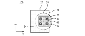
- Embodiment 1. 1 and 2 are cross-sectional views of an optical semiconductor device 100 according to the first embodiment.
- a plane perpendicular to the emitted light direction 81 of the optical semiconductor device 100 will be referred to as an XY plane, and a direction parallel to the emitted light direction 81 will be referred to as a Z direction.
- the optical semiconductor device 100 includes a stem 10 having a first surface 11 and a second surface 12 opposite to the first surface 11.
- a semiconductor laser 16 is provided on the first surface 11 side of the stem 10 .
- FIG. 1 is a YZ cross-sectional view passing through the center of the stem 10.
- FIG. 2 is a view of an XY section obtained by cutting FIG. 1 along the straight line AB, viewed from the second surface 12 side of the stem 10.
- the plurality of lead pins 30 penetrate the stem 10 from the first surface 11 to the second surface 12.
- the stem 10 and lead pins 30 are made of metal including iron or the like.
- the stem 10 and lead pins 30 may be plated with gold on their surfaces.
- the stem 10 has a disc shape, for example, with a diameter of 5.6 mm and a thickness of about 1.2 mm.
- the lead pin 30 has a diameter of 0.4 mm, for example.
- a portion of the lead pin 30 having a length of about 15 mm is pulled out from the second surface 12 side of the stem 10.
- a sealing material 32 made of an insulating material such as glass is filled between the stem 10 and the lead pins 30. Thereby, the stem 10 and the lead pins 30 are electrically insulated.
- the plurality of lead pins 30 may include ones that are electrically short-circuited to the stem 10.
- a mounting block 14 made of a metal material is mounted on the first surface 11 of the stem 10.
- a semiconductor laser 16 is mounted on the mounting block 14 so that light is emitted in the Z direction.
- the semiconductor laser 16 is, for example, an edge-emitting laser chip.
- the semiconductor laser 16 may be a surface emitting laser or an LED as long as it is a light emitting element.
- the semiconductor laser 16 and the lead pins 30 are electrically connected using a gold wire, a wiring board, or the like (not shown). By injecting current from the lead pin 30, the semiconductor laser 16 can be operated.
- a cylindrical lens barrel 34 made of metal is welded to the first surface 11 of the stem 10.
- a glass lens 36 is attached to the tip of the lens barrel 34.
- the lens barrel 34 and the glass lens 36 cover and seal the mounting block 14 and the semiconductor laser 16.
- the heat radiation block 20 has a third surface 23 and a fourth surface 24 opposite to the third surface 23, and the third surface 23 contacts the second surface 12 of the stem 10.
- the position of the stem 10 is indicated by a dashed line.
- the heat radiation block 20 is made of metal.
- the side surface 21 connecting the third surface 23 and the fourth surface 24 is cut out, and a groove 26 penetrating from the third surface 23 to the fourth surface 24 is formed.
- a plurality of lead pins 30 are inserted into the groove 26.
- the groove 26 is formed so that the heat radiation block 20 does not interfere with the lead pin 30.
- the groove 26 of the heat dissipation block 20 is rectangular, but it may also be polygonal, U-shaped, or the like.
- the depth of the groove 26 from the side surface 21 is, for example, greater than or equal to the distance between the plurality of lead pins 30.
- the outer peripheral portion of the second surface 12 of the stem 10 is in contact with the third surface 23 of the heat radiation block 20.
- An insulating film 28 made of polyimide or the like is provided on the inner surface of the heat radiation block 20 where the groove 26 is formed. Thereby, even if the lead pins 30 and the heat radiation block 20 come into contact with each other, electrical conduction between the lead pins 30 and the heat radiation block 20 can be suppressed.
- the semiconductor laser 16 When the lead pin 30 is connected to a power source and current is injected, the semiconductor laser 16 emits laser oscillation light.
- the laser oscillation light passes through the glass lens 36 and is emitted in the Z direction.
- heat is generated in the semiconductor laser 16 along with laser oscillation. This heat escapes from the mounting block 14, which has high thermal conductivity, through the stem 10, as shown by arrow 80.
- the heat dissipation block 20 by arranging the heat dissipation block 20 so as to be in contact with the second surface 12 of the stem 10, heat can be dissipated from the second surface 12 toward the heat dissipation block 20 through a short heat dissipation path. This can prevent the temperature of the semiconductor laser 16 from rising excessively during current injection. Therefore, deterioration in optical output characteristics and reliability can be suppressed.
- the package is often assembled so that the light emitting point of the semiconductor laser 16, which is the heat source, is located near the center of the stem 10. Therefore, when the heat radiation block 20 contacts the stem 10 in a region near the center of the second surface 12 of the stem 10, the heat radiation efficiency can be improved.
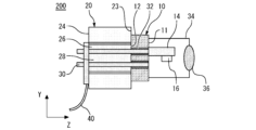
- FIG. 3 is a cross-sectional view of an optical semiconductor device 200 according to a first modification of the first embodiment.
- the flexible substrate 40 is connected to the lead pins 30 on the fourth surface 24 side of the heat dissipation block 20.
- a plurality of holes are formed in the flexible substrate 40 into which the lead pins 30 are inserted.
- the flexible substrate 40 has electrical wiring such as a wiring pattern.
- a comparative example of this embodiment consider a structure in which a heat dissipation block is provided with an insertion hole for a lead pin 30.
- the heat radiation block needs to be attached in the Z direction from the second surface 12 side of the stem 10. Therefore, in the comparative example, it is necessary to attach the heat dissipation block before attaching the flexible substrate 40 to the lead pins 30.
- the heat radiation block 20 according to the first embodiment can be attached to the stem 10 from two directions, the Z direction and the X direction. Therefore, in this embodiment, it is also possible to attach the heat dissipation block 20 to the stem 10 after attaching the flexible substrate 40 to the lead pins 30. As described above, in this embodiment, it is possible to increase the degree of freedom in the method of attaching the heat dissipation block 20 or the order of assembly, and it is possible to improve the flexibility of the manufacturing process.
- the lead pin 30 may be bent. Furthermore, interference between the heat radiation block and the lead pins 30 may make it impossible to attach the heat radiation block. Furthermore, the inside of the insertion hole, which is approximately several mm in diameter, must be covered with an insulator. For these reasons, high machining accuracy is required, which may increase the machining cost of the heat dissipation block. In contrast, in the present embodiment, there is no need to form an insertion hole in the heat dissipation block 20 and to form an insulator inside the insertion hole. Therefore, high processing accuracy is not required, and manufacturing costs can be suppressed.
- the heat dissipation block 20 and the lead pin 30 can be easily aligned. Therefore, the heat radiation block 20 can be easily attached to the stem 10. Therefore, assembly costs can be suppressed.
- the optical semiconductor device 100 can be easily manufactured.
- the heat dissipation block 20 of this embodiment can be manufactured using less metal material than the heat dissipation block in which insertion holes are formed according to the comparative example. Therefore, material costs can be suppressed.
- FIG. 4 is a cross-sectional view of an optical semiconductor device 300 according to a second modification of the first embodiment.
- the optical semiconductor device 300 differs from the optical semiconductor device 100 in the structure of the heat dissipation block 320.
- the other configurations are similar to those of the optical semiconductor device 100.
- a plurality of grooves 26 may be formed in the heat radiation block 320 in accordance with the arrangement of the lead pins 30.
- the contact area between the stem 10 and the heat radiation block 320 can be made larger than in the optical semiconductor device 100. Therefore, heat radiation efficiency can be improved.
- the shapes of the heat radiation block 20 and the grooves 26 of this embodiment are not limited to those shown in FIGS. 1 to 4.
- the heat radiation block 20 may be rectangular, polygonal, circular, oval, or the like when viewed from the Z direction.
- the groove 26 is not limited to a rectangular shape, but may be polygonal, U-shaped, or the like.
- the number of lead pins 30 is not limited.
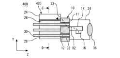
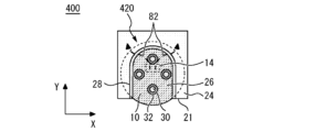
- Embodiment 2. 5 and 6 are cross-sectional views of an optical semiconductor device 400 according to the second embodiment.
- FIG. 5 is a YZ cross-sectional view passing through the center of the stem 10.
- FIG. 6 is a view of an XY section obtained by cutting FIG. 5 along the line CD, viewed from the second surface 12 side of the stem 10.
- Optical semiconductor device 400 differs from optical semiconductor device 100 in the structure of heat dissipation block 420. The other configurations are similar to those of the optical semiconductor device 100.
- the groove 26 is formed so that the Y direction is the depth direction. In other words, the groove 26 opens toward the negative direction of the Y-axis.
- the semiconductor laser 16 is arranged so that light is emitted from the center of the XY plane of the stem 10. For this reason, the mounting block 14 on which the semiconductor laser 16 is mounted is often placed at a position offset from the center of the stem 10. Also in this embodiment, the mounting block 14 on which the semiconductor laser 16 is mounted is provided at a position biased to one side from the center of the stem 10 on the first surface 11 of the stem 10 . One side is the positive Y-axis direction in FIG.
- the bottom of the groove 26 of the heat dissipation block 420 is provided on one side, that is, on the Y-axis positive direction side. Thereby, the distance between the bottom of the groove 26 of the heat radiation block 420 and the mounting block 14 can be reduced.
- the contact portion between the second surface 12 of the stem 10 and the heat radiation block 420 approaches the mounting block 14, so that the heat radiation path from the semiconductor laser 16 to the heat radiation block 420 can be shortened as shown by the arrow 82. . Therefore, heat radiation efficiency can be improved.
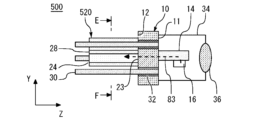
- Embodiment 3. 7 and 8 are cross-sectional views of an optical semiconductor device 500 according to the third embodiment.
- the optical semiconductor device 500 differs from the optical semiconductor device 100 in the structure of the heat dissipation block 520.
- Other configurations are similar to those of the first embodiment.
- FIG. 7 is a YZ cross-sectional view passing through the center of the stem 10.
- FIG. 8 is a view of an XY section obtained by cutting FIG. 7 along the line EF, viewed from the second surface 12 side of the stem 10.
- the third surface 23 of the heat radiation block 520 is in contact with the second surface 12 of the stem 10.
- the heat radiation block 520 has a shape that can be placed in the center of the second surface 12 of the stem 10, for example, between the plurality of lead pins 30. That is, the heat dissipation block 520 extends from the center of the second surface 12 of the stem 10 through between the plurality of lead pins 30.
- the heat radiation block 520 is, for example, a rectangular parallelepiped. That is, the heat radiation block 520 has a rectangular shape when viewed from a direction perpendicular to the second surface 12.
- An insulating film 28 made of polyimide or the like is provided on the side surface 21 of the heat radiation block 520 that connects the third surface 23 and the fourth surface 24.
- the insulating film 28 is provided to prevent conduction between the lead pin 30 and the heat radiation block 520.
- the insulating film 28 may be provided on the side surface 21 facing the lead pin 30.
- the optical semiconductor device 100 can be easily manufactured and material costs can be suppressed. Furthermore, in this embodiment, there is no need to form grooves in the heat dissipation block 520. Therefore, processing costs can be suppressed. Further, in this embodiment, since the heat radiation block 520 can be arranged at the center of the stem 10, the heat radiation path from the semiconductor laser 16 to the heat radiation block 520 can be shortened as shown by the arrow 83. Therefore, heat can be efficiently released.
- FIG. 9 is a cross-sectional view of an optical semiconductor device 600 according to a modification of the third embodiment.
- the optical semiconductor device 600 includes a heat radiation block 620.
- the heat radiation block 620 has a cross shape when viewed from a direction perpendicular to the second surface 12. In the heat radiation block 620, the contact area between the stem 10 and the heat radiation block 620 can be expanded more than in the heat radiation block 520. Therefore, heat dissipation efficiency can be improved.
- the heat radiation block 620 can only be attached to the stem 10 from the Z direction. Therefore, there are restrictions on the manufacturing process compared to the first embodiment.
- the flexible substrate 40 may be connected to the plurality of lead pins 30 on the fourth surface 24 side of the heat dissipation block 520.
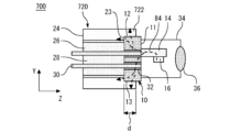
- FIG. 10 is a cross-sectional view of an optical semiconductor device 700 according to the fourth embodiment.
- FIG. 11 is a perspective view of a heat radiation block 720 according to the fourth embodiment.
- the optical semiconductor device 700 is different from the optical semiconductor device 100 in the structure of the heat radiation block 720.
- Other configurations are similar to those of the first embodiment.
- the heat radiation block 720 has a semicircular shape when viewed from the Z direction, for example. Similar to the heat radiation block 20, the heat radiation block 720 is formed with a groove 26 through which the lead pin 30 is passed.
- the heat radiation block 720 has a stepped portion 722 that extends from the third surface 23 toward the stem 10 and contacts the side surface 13 connecting the first surface 11 and the second surface 12 of the stem 10 .
- the stepped portion 722 has a height d from the third surface 23.
- the heat dissipation block 720 contacts the second surface 12 and side surface 13 of the stem 10 . Therefore, as shown by the arrow 84, a heat radiation path from the side surface of the stem 10 to the heat radiation block 720 is added, so that heat can be dissipated more efficiently.
- the height d is greater than or equal to the thickness of the stem 10
- the contact area between the stepped portion 722 and the side surface 13 of the stem 10 is maximized, and heat dissipation is also maximized.
- the stepped portion 722 also functions as an assembly guide. The step portion 722 allows the positional relationship between the stem 10 and the heat radiation block 720 to be determined, thereby suppressing assembly misalignment.
- FIG. 12 is a cross-sectional view of an optical semiconductor device 800 according to the fifth embodiment.
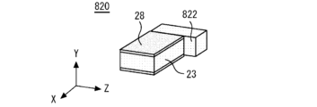
- FIG. 13 is a perspective view of a heat dissipation block according to the fifth embodiment.
- Optical semiconductor device 800 differs from optical semiconductor device 500 in the structure of heat dissipation block 820. Other configurations are similar to those of the third embodiment.
- the step portion of the fourth embodiment is provided in the heat dissipation block of the third embodiment.
- the heat dissipation block 820 extends from the center of the second surface 12 of the stem 10 and passes between the plurality of lead pins 30 .
- the heat radiation block 820 has a stepped portion 822 that extends from the third surface 23 toward the stem 10 and comes into contact with the side surface 13 of the stem 10 .
- the heat radiation block 820 is in contact with the second surface 12 and side surface 13 of the stem 10. Therefore, compared to Embodiment 3, heat can be dissipated more efficiently in this embodiment.
- the center of the stem 10 near the semiconductor laser 16 contacts the heat radiation block 820, so that heat can be efficiently radiated from the second surface 12 of the stem 10.
- the contact area between the side surface 13 of the stem 10 and the stepped portion 822 is smaller than in the fourth embodiment. Therefore, the efficiency of heat radiation from the side surface 13 of the stem 10 is higher in the fourth embodiment.
- the step portion 822 can suppress assembly misalignment.
Landscapes
- Physics & Mathematics (AREA)
- Condensed Matter Physics & Semiconductors (AREA)
- General Physics & Mathematics (AREA)
- Electromagnetism (AREA)
- Optics & Photonics (AREA)
- Semiconductor Lasers (AREA)
Abstract
Description
第2の開示に係る光半導体装置では、放熱ブロックはステムの第2面の中心部から複数のリードピンの間を通って延びる。このため、放熱ブロックに挿通孔を形成する必要がなく、光半導体装置を容易に製造できる。
図1、2は、実施の形態1に係る光半導体装置100の断面図である。以下では、光半導体装置100の出射光方向81に垂直な面をXY平面、出射光方向81に平行な方向をZ方向とする。光半導体装置100は、第1面11と、第1面11と反対側の第2面12と、を有するステム10を備える。ステム10の第1面11側には半導体レーザ16が設けられる。図1は、ステム10の中心を通るYZ断面図である。図2は図1をA-B直線で切断することで得られるXY断面をステム10の第2面12側から見た図である。
図5、6は、実施の形態2に係る光半導体装置400の断面図である。図5はステム10の中心を通るYZ断面図である。図6は図5をC-D直線で切断することで得られるXY断面をステム10の第2面12側から見た図である。光半導体装置400は、放熱ブロック420の構造が光半導体装置100と異なる。他の構成は光半導体装置100の構成と同様である。放熱ブロック420の側面21において、溝26はY方向が深さ方向となるように形成されている。つまり、溝26はY軸負方向に向かって開口している。
図7、8は、実施の形態3に係る光半導体装置500の断面図である。光半導体装置500は放熱ブロック520の構造が光半導体装置100と異なる。他の構成は、実施の形態1の構成と同様である。図7はステム10の中心を通るYZ断面図である。図8は図7をE-F直線で切断することで得られるXY断面をステム10の第2面12側から見た図である。
図10は、実施の形態4に係る光半導体装置700の断面図である。図11は、実施の形態4に係る放熱ブロック720の斜視図である。光半導体装置700は放熱ブロック720の構造が光半導体装置100と異なる。他の構成は、実施の形態1の構成と同様である。放熱ブロック720は例えばZ方向から見て半円形である。放熱ブロック720には、放熱ブロック20と同様にリードピン30を通す溝26が形成されている。さらに放熱ブロック720は、第3面23からステム10側に延び、ステム10の第1面11と第2面12とを繋ぐ側面13と接触する段差部722を有する。段差部722は第3面23からの高さdを有する。
図12は、実施の形態5に係る光半導体装置800の断面図である。図13は、実施の形態5に係る放熱ブロックの斜視図である。光半導体装置800は放熱ブロック820の構造が光半導体装置500と異なる。他の構成は、実施の形態3の構成と同様である。本実施の形態では、実施の形態3の放熱ブロックに実施の形態4の段差部が設けられている。放熱ブロック820は、ステム10の第2面12の中心部から複数のリードピン30の間を通って延びる。放熱ブロック820は、第3面23からステム10側に延び、ステム10の側面13と接触する段差部822を有する。
Claims (10)
- 第1面と、前記第1面と反対側の第2面と、を有するステムと、
前記ステムの前記第1面側に設けられた半導体レーザと、
前記ステムを前記第1面から前記第2面に貫通するリードピンと、
第3面と、前記第3面と反対側の第4面と、を有し、前記第3面が前記ステムの前記第2面と接触する放熱ブロックと、
を備え、
前記放熱ブロックには、前記第3面と前記第4面を繋ぐ側面を切り欠き、前記第3面から前記第4面に貫通する溝が形成され、
前記溝を形成する前記放熱ブロックの内側面には絶縁膜が設けられ、
前記リードピンは前記放熱ブロックの前記溝に挿入されることを特徴とする光半導体装置。 - 前記第1面のうち前記ステムの中心から一方の側に偏った位置に設けられ、前記半導体レーザが搭載された実装ブロックを備え、
前記溝の底部は前記一方の側に設けられることを特徴とする請求項1に記載の光半導体装置。 - 前記放熱ブロックには複数の前記溝が形成されたことを特徴とする請求項1または2に記載の光半導体装置。
- 前記放熱ブロックは、前記第3面から前記ステム側に延び、前記ステムの前記第1面と前記第2面とを繋ぐ側面と接触する段差部を有することを特徴とする請求項1から3の何れか1項に記載の光半導体装置。
- 前記放熱ブロックの前記第4面側で前記リードピンに接続されるフレキシブル基板を備えることを特徴とする請求項1から4の何れか1項に記載の光半導体装置。
- 第1面と、前記第1面と反対側の第2面と、を有するステムと、
前記ステムの前記第1面側に設けられた半導体レーザと、
前記ステムを前記第1面から前記第2面に貫通する複数のリードピンと、
第3面と、前記第3面と反対側の第4面と、を有し、前記第3面が前記ステムの前記第2面と接触する放熱ブロックと、
を備え、
前記第3面と前記第4面と繋ぐ前記放熱ブロックの側面には、絶縁膜が設けられ、
前記放熱ブロックは、前記ステムの前記第2面の中心部から前記複数のリードピンの間を通って延びることを特徴とする光半導体装置。 - 前記放熱ブロックは、前記第2面と垂直な方向から見て長方形であることを特徴とする請求項6に記載の光半導体装置。
- 前記放熱ブロックは、前記第2面と垂直な方向から見て十字型であることを特徴とする請求項6に記載の光半導体装置。
- 前記放熱ブロックは、前記第3面から前記ステム側に延び、前記ステムの前記第1面と前記第2面を繋ぐ側面と接触する段差部を有することを特徴とする請求項6から8の何れか1項に記載の光半導体装置。
- 前記放熱ブロックの前記第4面側で前記複数のリードピンに接続されるフレキシブル基板を備えることを特徴とする請求項6から9の何れか1項に記載の光半導体装置。
Priority Applications (5)
| Application Number | Priority Date | Filing Date | Title |
|---|---|---|---|
| JP2024522835A JP7652340B2 (ja) | 2022-05-26 | 2022-05-26 | 光半導体装置 |
| US18/838,438 US20250158355A1 (en) | 2022-05-26 | 2022-05-26 | Optical semiconductor device |
| CN202280096267.8A CN119301829A (zh) | 2022-05-26 | 2022-05-26 | 光半导体装置 |
| PCT/JP2022/021591 WO2023228367A1 (ja) | 2022-05-26 | 2022-05-26 | 光半導体装置 |
| TW112117316A TWI846460B (zh) | 2022-05-26 | 2023-05-10 | 光半導體裝置 |
Applications Claiming Priority (1)
| Application Number | Priority Date | Filing Date | Title |
|---|---|---|---|
| PCT/JP2022/021591 WO2023228367A1 (ja) | 2022-05-26 | 2022-05-26 | 光半導体装置 |
Publications (1)
| Publication Number | Publication Date |
|---|---|
| WO2023228367A1 true WO2023228367A1 (ja) | 2023-11-30 |
Family
ID=88918769
Family Applications (1)
| Application Number | Title | Priority Date | Filing Date |
|---|---|---|---|
| PCT/JP2022/021591 Ceased WO2023228367A1 (ja) | 2022-05-26 | 2022-05-26 | 光半導体装置 |
Country Status (5)
| Country | Link |
|---|---|
| US (1) | US20250158355A1 (ja) |
| JP (1) | JP7652340B2 (ja) |
| CN (1) | CN119301829A (ja) |
| TW (1) | TWI846460B (ja) |
| WO (1) | WO2023228367A1 (ja) |
Citations (6)
| Publication number | Priority date | Publication date | Assignee | Title |
|---|---|---|---|---|
| JP2003188456A (ja) * | 2001-12-19 | 2003-07-04 | Hitachi Ltd | 光電子装置 |
| JP2008034640A (ja) * | 2006-07-28 | 2008-02-14 | Ricoh Printing Systems Ltd | 半導体装置及び該半導体装置における放熱方法 |
| WO2010140473A1 (ja) * | 2009-06-02 | 2010-12-09 | 三菱電機株式会社 | 半導体光変調装置 |
| JP2011018800A (ja) * | 2009-07-09 | 2011-01-27 | Sharp Corp | 半導体レーザ装置 |
| JP2018018995A (ja) * | 2016-07-29 | 2018-02-01 | 株式会社ヨコオ | 光モジュール |
| JP2020126987A (ja) * | 2019-02-06 | 2020-08-20 | ウシオ電機株式会社 | 半導体レーザ光源装置 |
Family Cites Families (3)
| Publication number | Priority date | Publication date | Assignee | Title |
|---|---|---|---|---|
| US7653099B2 (en) * | 2004-06-02 | 2010-01-26 | Panasonic Corporation | Semiconductor laser device which is capable of stably emitting short-wavelength laser light |
| JP2007053242A (ja) * | 2005-08-18 | 2007-03-01 | Fuji Xerox Co Ltd | 半導体レーザ装置およびその製造方法 |
| WO2013080396A1 (ja) * | 2011-11-30 | 2013-06-06 | パナソニック株式会社 | 窒化物半導体発光装置 |
-
2022
- 2022-05-26 US US18/838,438 patent/US20250158355A1/en active Pending
- 2022-05-26 JP JP2024522835A patent/JP7652340B2/ja active Active
- 2022-05-26 CN CN202280096267.8A patent/CN119301829A/zh active Pending
- 2022-05-26 WO PCT/JP2022/021591 patent/WO2023228367A1/ja not_active Ceased
-
2023
- 2023-05-10 TW TW112117316A patent/TWI846460B/zh active
Patent Citations (6)
| Publication number | Priority date | Publication date | Assignee | Title |
|---|---|---|---|---|
| JP2003188456A (ja) * | 2001-12-19 | 2003-07-04 | Hitachi Ltd | 光電子装置 |
| JP2008034640A (ja) * | 2006-07-28 | 2008-02-14 | Ricoh Printing Systems Ltd | 半導体装置及び該半導体装置における放熱方法 |
| WO2010140473A1 (ja) * | 2009-06-02 | 2010-12-09 | 三菱電機株式会社 | 半導体光変調装置 |
| JP2011018800A (ja) * | 2009-07-09 | 2011-01-27 | Sharp Corp | 半導体レーザ装置 |
| JP2018018995A (ja) * | 2016-07-29 | 2018-02-01 | 株式会社ヨコオ | 光モジュール |
| JP2020126987A (ja) * | 2019-02-06 | 2020-08-20 | ウシオ電機株式会社 | 半導体レーザ光源装置 |
Also Published As
| Publication number | Publication date |
|---|---|
| US20250158355A1 (en) | 2025-05-15 |
| JP7652340B2 (ja) | 2025-03-27 |
| TWI846460B (zh) | 2024-06-21 |
| CN119301829A (zh) | 2025-01-10 |
| JPWO2023228367A1 (ja) | 2023-11-30 |
| TW202347908A (zh) | 2023-12-01 |
Similar Documents
| Publication | Publication Date | Title |
|---|---|---|
| US10819084B2 (en) | TO-CAN packaged laser and optical module | |
| US11349278B2 (en) | Stem for semiconductor package, and semiconductor package | |
| US10692825B2 (en) | Light-emitting chip package | |
| US20190260179A1 (en) | Light emitting element housing package, light emitting device, and light emitting module | |
| KR100568275B1 (ko) | Pcb타입 리드프레임을 갖는 반도체 레이저 다이오드장치 | |
| KR20060051982A (ko) | 반도체 장치 및 전자기기 | |
| CN110233138B (zh) | 半导体发光装置 | |
| CN100483872C (zh) | 半导体激光装置和光学拾波装置 | |
| JP6225834B2 (ja) | 半導体発光装置およびその製造方法 | |
| KR20100102661A (ko) | 반도체 레이저 장치 | |
| WO2023228367A1 (ja) | 光半導体装置 | |
| JP4951691B2 (ja) | 光伝送モジュールおよびこれを用いた光通信装置 | |
| US20210265812A1 (en) | Semiconductor laser device | |
| US20190115719A1 (en) | Semiconductor light-emitting element and semiconductor light-emitting device | |
| WO2021166215A1 (ja) | 半導体レーザ装置 | |
| US7567599B2 (en) | Semiconductor laser diode device with thermal conductive encapsulating resin and method for manufacturing the same | |
| JP2007059677A (ja) | 発光ダイオード装置 | |
| US12264810B2 (en) | Lighting device and a method of manufacturing a lighting device | |
| KR20220164440A (ko) | 레이저 다이오드 패키지 | |
| JP6485518B2 (ja) | 半導体発光装置およびその製造方法 | |
| KR100568274B1 (ko) | 리드프레임 일체형 반도체 레이저 다이오드장치 | |
| WO2026071235A1 (ja) | 光素子搭載用パッケージ及び発光装置 | |
| JP2008060301A (ja) | 半導体レーザ装置 | |
| JP2023166838A (ja) | 半導体発光装置 | |
| JP2021022631A (ja) | 光源装置 |
Legal Events
| Date | Code | Title | Description |
|---|---|---|---|
| 121 | Ep: the epo has been informed by wipo that ep was designated in this application |
Ref document number: 22943767 Country of ref document: EP Kind code of ref document: A1 |
|
| WWE | Wipo information: entry into national phase |
Ref document number: 2024522835 Country of ref document: JP |
|
| WWE | Wipo information: entry into national phase |
Ref document number: 18838438 Country of ref document: US |
|
| WWE | Wipo information: entry into national phase |
Ref document number: 202280096267.8 Country of ref document: CN |
|
| NENP | Non-entry into the national phase |
Ref country code: DE |
|
| WWP | Wipo information: published in national office |
Ref document number: 202280096267.8 Country of ref document: CN |
|
| WWP | Wipo information: published in national office |
Ref document number: 18838438 Country of ref document: US |
|
| 122 | Ep: pct application non-entry in european phase |
Ref document number: 22943767 Country of ref document: EP Kind code of ref document: A1 |