WO2023219107A1 - インバータ回路および無線電力伝送回路 - Google Patents
インバータ回路および無線電力伝送回路 Download PDFInfo
- Publication number
- WO2023219107A1 WO2023219107A1 PCT/JP2023/017590 JP2023017590W WO2023219107A1 WO 2023219107 A1 WO2023219107 A1 WO 2023219107A1 JP 2023017590 W JP2023017590 W JP 2023017590W WO 2023219107 A1 WO2023219107 A1 WO 2023219107A1
- Authority
- WO
- WIPO (PCT)
- Prior art keywords
- circuit
- power
- inverter circuit
- power supply
- load
- Prior art date
- Legal status (The legal status is an assumption and is not a legal conclusion. Google has not performed a legal analysis and makes no representation as to the accuracy of the status listed.)
- Ceased
Links
Images




Classifications
-
- H—ELECTRICITY
- H02—GENERATION; CONVERSION OR DISTRIBUTION OF ELECTRIC POWER
- H02J—ELECTRIC POWER NETWORKS; CIRCUIT ARRANGEMENTS OR SYSTEMS FOR SUPPLYING OR DISTRIBUTING ELECTRIC POWER; SYSTEMS FOR STORING ELECTRIC ENERGY
- H02J50/00—Circuit arrangements or systems for wireless supply or distribution of electric power
- H02J50/10—Circuit arrangements or systems for wireless supply or distribution of electric power using inductive coupling
- H02J50/12—Circuit arrangements or systems for wireless supply or distribution of electric power using inductive coupling of the resonant type
-
- H—ELECTRICITY
- H02—GENERATION; CONVERSION OR DISTRIBUTION OF ELECTRIC POWER
- H02M—APPARATUS FOR CONVERSION BETWEEN AC AND AC, BETWEEN AC AND DC, OR BETWEEN DC AND DC, AND FOR USE WITH MAINS OR SIMILAR POWER SUPPLY SYSTEMS; CONVERSION OF DC OR AC INPUT POWER INTO SURGE OUTPUT POWER; CONTROL OR REGULATION THEREOF
- H02M7/00—Conversion of AC power input into DC power output; Conversion of DC power input into AC power output
- H02M7/42—Conversion of DC power input into AC power output without possibility of reversal
- H02M7/44—Conversion of DC power input into AC power output without possibility of reversal by static converters
- H02M7/48—Conversion of DC power input into AC power output without possibility of reversal by static converters using discharge tubes with control electrode or semiconductor devices with control electrode
-
- H—ELECTRICITY
- H02—GENERATION; CONVERSION OR DISTRIBUTION OF ELECTRIC POWER
- H02M—APPARATUS FOR CONVERSION BETWEEN AC AND AC, BETWEEN AC AND DC, OR BETWEEN DC AND DC, AND FOR USE WITH MAINS OR SIMILAR POWER SUPPLY SYSTEMS; CONVERSION OF DC OR AC INPUT POWER INTO SURGE OUTPUT POWER; CONTROL OR REGULATION THEREOF
- H02M7/00—Conversion of AC power input into DC power output; Conversion of DC power input into AC power output
- H02M7/42—Conversion of DC power input into AC power output without possibility of reversal
- H02M7/44—Conversion of DC power input into AC power output without possibility of reversal by static converters
- H02M7/48—Conversion of DC power input into AC power output without possibility of reversal by static converters using discharge tubes with control electrode or semiconductor devices with control electrode
- H02M7/4815—Resonant converters
-
- H—ELECTRICITY
- H02—GENERATION; CONVERSION OR DISTRIBUTION OF ELECTRIC POWER
- H02J—ELECTRIC POWER NETWORKS; CIRCUIT ARRANGEMENTS OR SYSTEMS FOR SUPPLYING OR DISTRIBUTING ELECTRIC POWER; SYSTEMS FOR STORING ELECTRIC ENERGY
- H02J2207/00—Details of circuit arrangements for charging or discharging batteries or supplying loads from batteries
- H02J2207/20—Charging or discharging characterised by the power electronics converter
Definitions
- the present invention relates to inverter circuits that convert DC power to AC power, and wireless power transmission circuits that perform wireless power transmission using AC power converted by these inverter circuits.
- WPT wireless power transfer
- the secondary batteries that power these wireless power transfers are designed to prevent battery deterioration due to heat generation, such as the lithium-ion batteries that are widely used in mobile terminals such as mobile phones.
- the resonant converter has a problem in that it cannot perform both constant current power supply corresponding to constant current charging and constant voltage power supply corresponding to constant voltage charging.
- the present invention was made with attention to such problems, and an object of the present invention is to provide an inverter circuit and a wireless power transfer circuit that are capable of both constant current power supply and constant voltage power supply.
- the inverter circuit according to claim 1 includes: An inverter circuit connected to a DC power source and converting DC power output from the DC power source into AC power, an input inductor connected in series between the DC power supply and a switching circuit constituting an inverter circuit; a resonant circuit connected in parallel to the DC power supply together with the switching circuit, the resonant circuit including a resonant capacitor and a resonant inductor; a switch having one end connected to the DC power supply and the other end connected to the resonant capacitor and the resonant inductor; has the resonant inductor and the input inductor are connected in parallel to the switch; It is characterized by having the following. According to this feature, by switching the switch, it is possible to perform both constant current power supply and constant voltage power supply with one inverter circuit.
- the inverter circuit according to claim 2 is the inverter circuit according to claim 1, the inductance of the resonant inductor is smaller than the inductance of the input inductor;
- the constants of each element constituting the inverter circuit are optimized so that constant current power supply and constant voltage power supply are possible without depending on fluctuations in the power load to which the AC power output from the inverter circuit is supplied. It is characterized by being According to this feature, for example, by making the resonant inductor sufficiently small, one tenth or less of the inductance of the input inductor, constant current power supply and constant voltage that are independent of load fluctuations can be achieved without adding a new control mechanism.
- the circuit configuration for performing control corresponding to load fluctuations can be simplified.
- the wireless power transfer circuit according to claim 3 includes: An inverter circuit according to claim 2; A power transmission circuit that transmits power in a disconnected state by magnetic field resonance or electric field resonance; It is characterized by including. According to this feature, by switching a switch, one wireless power transmission circuit can control both constant current power supply and constant voltage power supply in response to load fluctuations, while simplifying the circuit configuration. It can be carried out.
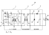
- FIG. 1 is a circuit diagram showing a wireless power transmission circuit to which an inverter circuit of the present invention is applied.
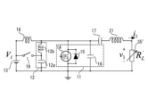
- 2 is a diagram showing an equivalent circuit of the wireless power transfer circuit of FIG. 1.
- FIG. FIG. 6 is a diagram showing a state of constant current power supply in an equivalent circuit by opening a changeover switch. It is a figure which shows the state of constant voltage power supply in an equivalent circuit by closing a changeover switch.
- FIG. 2 is an explanatory diagram illustrating a method of setting a load-independent EF class inverter (E/F class inverter).
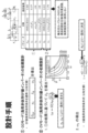
- FIG. 3 is an explanatory diagram showing a design procedure for an inverter circuit according to the present invention.
- FIG. 2 is a diagram showing an external photograph of a prototype inverter circuit and design values and measured values of each element used in the inverter circuit.
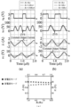
- FIG. 3 is a diagram showing a characteristic graph of a prototype inverter circuit.
- FIG. 3 is a circuit diagram showing a wireless power transmission circuit to which a modified inverter circuit is applied.
- 1 is a diagram showing the configuration of a conventional wireless power transmission device.
- FIG. 1 is a circuit diagram showing an example of a wireless power transfer circuit M to which the inverter circuit of the present invention is applied.
- the wireless power transmission circuit M to which the inverter circuit of the present invention is applied is a circuit section that mainly transmits power in an unconnected state by magnetic field resonance, and includes a power transmission coil (L1) 21
- the power transmission circuit section 2 consists of a pair of electromagnetic coils, the power receiving coil (L3) 22, the inverter circuit section 1 that supplies AC power at a predetermined frequency to the power transmitting coil (L1) 21, and the power receiving coil (L3) 22. It is comprised of a rectifier circuit section 3 that converts received AC power into DC power and supplies it to a power load (RL) 35.
- the power load (RL) 35 is assumed to be one that charges with DC power, such as a secondary battery, and whose load (resistance) changes over time as the DC power is supplied. It is not limited to these secondary batteries.
- Known electromagnetic coils can be used as the power transmission coil (L1) 21 and power reception coil (L3) 22 used in the power transmission circuit section 2, and the size of the power required for transmission, the frequency used for transmission, In addition, an appropriate one may be selected depending on the transmission distance, etc.
- a matching circuit is selected so that the Poincaré length is the shortest. may be provided.
- the rectifier circuit section 3 may be of any type as long as it can convert the AC power received by the power receiving coil (L3) 22 into DC power and stably supply it to the power load (RL) 35.
- a passive circuit is constructed of a diode (D2) 33 and a capacitor (CF) 34 connected in parallel to the load, and a capacitor (C3) 31 and a diode (D1) 32 connected in series to the load.
- a known class D rectifier can be suitably used as a circuit, and the parameters of each of these elements may be appropriately set according to the impedance of the power load (RL) 35 and the like.
- the inverter circuit unit 1 that supplies AC power to the power transmission coil (L1) 21 includes a switching circuit 11 for converting DC power output from the DC power supply 13 into AC power of a predetermined frequency;
- a series filter is formed by a combination of a high frequency resonant circuit 12 connected to a DC power supply 13 in parallel with the switching circuit 11, an input inductor (LC) 18, a changeover switch (S2) 19, and a power transmission coil (L1) 21. It mainly consists of an output capacitor (C1) 17 for.
- the switching circuit 11 connected to the power transmission coil (L1) 21 via the output capacitor (C1) 17 has a switching element (S1) 14 made of, for example, a gallium nitride N-channel MOS-FET.
- a diode 15 is connected in antiparallel to S1) 14, and a capacitance capacitor (CS) 16 is also connected.
- the switching element (S1) 14 is turned off.
- charge is accumulated in the capacitance capacitor (CS) 16
- all the charges accumulated in the capacitance capacitor (CS) 16 are released before the switching element (S1) 14 shifts to the on state, resulting in zero-volt switching ( ZVS (see FIG. 8) can be achieved.
- the circuit configuration may be such that the diode 15 is omitted.
- the switching circuit 11 is connected in series with the DC power supply 13 via an input inductor (LC) 18, and in parallel with the switching circuit 11, a high frequency resonant capacitor (C2) 12a and a high frequency resonant inductor (L2) 12b are connected.
- a high frequency resonant circuit 12 including a high frequency resonant circuit 12 is connected between an input inductor (LC) 18 and the switching circuit 11.
- a selector switch (S2) 19 is provided so that a short circuit can be made between the high frequency resonant capacitor (C2) 12a and the high frequency resonant inductor (L2) 12b and the DC power supply 13.
- the changeover switch (S2) 19 is a switch whose one end is connected to the DC power supply 13 and whose other end is connected to the high frequency resonant capacitor (C2) 12a and the high frequency resonant inductor (L2) 12b.
- the high frequency resonant inductor (L2) 12b of the present invention has a sufficiently smaller inductance (Lc>>L2) than the input inductor (LC) 18, and as described later, the selector switch (S2) 19 It is necessary to use an inductor that allows most of the current to flow through the high frequency resonant inductor (L2) 12b side rather than the input inductor (LC) 18 side when the inductor is closed and turned on. Specifically, it is preferable that the inductance of the high frequency resonant inductor (L2) 12b is about 1/10 to 1/100 of the inductance of the input inductor (LC) 18.
- the rectifier circuit section 3 has no input reactance, and the equivalent resistance on the power receiving side as seen from the inverter circuit section 1 side is based on the power that changes depending on the power load (RL) 35. Since it can be considered as a load (R'L), the circuit shown in FIG. 1 can be expressed as an equivalent circuit shown in FIG. 2 for convenience. Assumed to be performed.
- FIG. 3 is an explanatory diagram illustrating the operating situation when the changeover switch (S2) 19 is opened (OFF) in the equivalent circuit shown in FIG. 2.
- the changeover switch (S2) 19 is open (OFF)
- the input inductor current iC flows through the input inductor (LC) 18, and the high frequency current i2 (not shown) flows through the high frequency resonant circuit 12.
- 0.415 is determined as the duty ratio D in the switching element (S1) 14, and ⁇ B defined by ⁇ LB/R'L and ⁇ Regarding the correlation graph (design curve graph) with ⁇ S defined by
- the duty ratio D of the switching element (S1) 14 is set to 0.300 (not shown in the correlation graph). All you have to do is decide.
- ⁇ in the above definition formula is the operating angular frequency of switching by the switching element (S1) 14, and in FIG.
- the inductance of the rear-stage coil LB close to the power load R'L is used.
- the reason why the power transmitting coil (L1) 21 is regarded as the front-stage coil LA and the rear-stage coil LB is because of the component (LA) that resonates with the output capacitor (C1) 17 at the operating frequency of 1 MHz and the output. This is because it is necessary to perform circuit analysis separately for the inductive component (LB) that causes the current phase difference.
- the output capacitor (C1) 17 and the preceding coil LA are It is completely tuned to the frequency ⁇ , and the operating angular frequency ⁇ satisfies sqrt(C1 ⁇ LA).
- FIG. 4 is an explanatory diagram illustrating the operating situation when the changeover switch (S2) 19 is closed (ON) in the equivalent circuit shown in FIG. 2.
- the selector switch (S2) 19 is closed (ON)
- the voltage applied to the high frequency resonance capacitor (C2) 12a is clamped to the voltage V1 of the DC power supply 13.
- the inductance of the high frequency resonant inductor (L2) 12b is sufficiently smaller than the inductance of the input inductor (LC) 18 (Lc>>L2), most of the input current flows through the changeover switch (S2). 19 and the high frequency resonant inductor (L2) 12b. Therefore, the high-frequency resonant inductor (L2) 12b constitutes an apparent input inductance, achieving an operation called class E load independence, and the output voltage V1 is independent of the load fluctuation of the power load R'L. It remains almost constant.
- the design procedure for obtaining appropriate values of each element and parameters of the inverter circuit section 1 of the present invention will be explained in more detail using FIG. 7.
- the input voltage VI The inductance of the power transmission coil (L1) 21, the inductance of the input inductor (LC) 18, and the load resistance value are given.
- the inductance of the power transmission coil (L1) 21 and the input inductor (LC) 18 is given an appropriate value to serve as a resonance frequency and RF choke, and the load resistance value is given as RE for a constant current feeding class E inverter.
- REF constant current feeding class inverter.
- each element value and each parameter of a load-independent E/F class inverter with constant voltage power supply is designed.
- the duty ratio DEF in the switching element (S1) 14 is given for this design.
- Publicly known literature S. Aldhaher, D. C. Yates and P. D. Mitcheson, "Load-Independent Class E/EF Inverters and Rectifiers for MHz-Switching Applications," IEEE Transactions on Power Electronics, vol. 33, no In accordance with the design theory of load-independent E/F class inverters shown in . Parameter ⁇ S, parameter ⁇ B, and parameter ⁇ 2 are derived.
- the inductance of the power transmission coil (L1) 21 uses the value given initially, and the element values of the capacitance capacitor (CS) 16 and the output capacitor (C1) 17 are determined in the first step above. It must be the same as the element value.
- the duty ratio DE in the switching element (S1) 14 of the E-class inverter and the high-frequency resonant inductor (L2) 12b to satisfy the load-independent condition while satisfying the conditions of the load-independent E/F class inverter are determined.
- the inductance of can be uniquely determined.
- the duty ratio DE is determined using a design curve graph shown in FIG. 5 with dimensionless parameters in which the horizontal axis is the parameter ⁇ B and the vertical axis is the parameter ⁇ S.
- the parameter ⁇ B 1, which is the design value determined in the design stage (first stage) of the load-independent E/F class inverter.
- the curve in the design curve graph shown in FIG. 5 is the design value of the rear-stage coil LB and the capacitance capacitor (CS) 16 at the duty ratio DE in the switching element (S1) 14 of the class E inverter. At this time, it can be seen that the design curve passes through the star mark only when the duty ratio DE is 0.415.
- the duty ratio DE of the load-independent class E inverter is determined to be 0.415, and based on the determined duty ratio DE, the parameter ⁇ S is set as shown in the above-mentioned known document, as shown in FIG. It can be derived from the class E load independent conditional expression, and the inductance of the high frequency resonant inductor (L2) 12b is determined by these derived parameters ⁇ S. Furthermore, from the inductance of the high-frequency resonant inductor (L2) 12b determined in this way and the resonant frequency determined in the design stage (first stage) of the load-independent E/F class inverter, the high-frequency resonant capacitor (C2) 12a is calculated. Since the capacitance can also be determined, all element values are determined.
- the present invention satisfies constant current power supply (CC mode) and constant voltage power supply (CV mode), which are called load independent, by ON/OFF switching of the changeover switch (S2) 19.
- CC mode constant current power supply
- CV mode constant voltage power supply
- S2 changeover switch
- Optimization of constants means “determining element values so as to satisfy each of the above-mentioned conditions.”
- the design procedure shown above is just an example, and the method of deriving element values that satisfy all of the conditions is not limited to the design procedure described above. It goes without saying that element values that satisfy all of the following conditions may be derived.
- each element value derived by the design procedure described above is just a design value, and there may be an error from the actual element value of the component as shown in FIG. 7 described later.
- the efficiency of class E circuits used under high-frequency operation is robust to variations in element values due to individual differences in elements, so even if variations in element values occur, there is no effect on circuit operation such as efficiency. Since the value is limited, an error from the design value can be tolerated within a range where necessary and sufficient performance can be obtained in terms of efficiency, etc.
- FIG. 7 is a prototype showing an inverter circuit board to which the inverter circuit of the present invention is applied.
- the inverter circuit board is a small board measuring 40 mm x 50 mm. As shown in FIG. 7, the board is provided with three coils consisting of an input inductor (LC) 18, a high frequency resonant inductor (L2) 12b, and a power transmission coil (L1) 21, and the largest power transmission coil (L1). ) 21, a capacitance capacitor (CS) 16, an output capacitor (C1) 17, and a high frequency resonance capacitor (C2) 12a are mounted using ceramic capacitors.
- LC input inductor
- L2 high frequency resonant inductor
- L1 power transmission coil
- L1 the largest power transmission coil
- C1 the largest power transmission coil
- C2 high frequency resonance capacitor
- the inverter circuit board is wire-connected to a 24V DC power supply 13 via three terminals provided near an input inductor (LC) 18, and is also connected to a 24V DC power supply 13 via three terminals provided near an input inductor (LC) 18. It is wired to a manual selector switch (S2) 19 through two terminals, and by manually switching ON/OFF of the selector switch (S2) 19, load-independent constant current operation and load-independent constant current operation can be achieved. It is now possible to switch between dependent type constant voltage operation.
- the designed operating frequency fs of the prototype inverter circuit board is 1 MHz
- the input DC voltage V1 is 24.0 V
- the inductance of the input inductor (LC) 18 is 100 ⁇ H
- the inductance of the power transmission coil (L1) 21 is 11.
- the inductance of the high frequency resonant inductor (L2) 12b is 3.24 ⁇ H
- the capacitance of the capacitive capacitor (CS) 16 is 5.50 nF
- the capacitance of the output capacitor (C1) 17 is 2.43 nF
- the inductance of the high frequency resonant inductor (C2) 12a is 9 ⁇ H.
- the inductance of the high frequency resonant inductor (L2) 12b is approximately 1/31 of the inductance of the input inductor (LC) 18.
- FIG. 8 shows the results of actually measuring the voltage V1 and current i1 applied to the circuit.
- FIG. 8(a) is a graph showing the measurement results when the changeover switch (S2) 19 is opened (OFF).
- the changeover switch (S2) 19 is opened (OFF)
- the power load R'L becomes 1/10, 1/2, or 1/1 of R(LEF).
- the voltage V1 changes, the voltage V1 applied to the power load R'L changes greatly, but the current i1 hardly changes, indicating that constant current power supply is being performed, and the switching by the switching element (S1) 14. It can be seen that when this is executed, both the voltage VS and the voltage Vg are 0V, and zero volt switching (ZVS) is realized.
- FIG. 8(b) is a graph showing the measurement results when the changeover switch (S2) 19 is closed (ON).
- the power load R'L is 1/10, 1/2, or 1/1 of R(LEF).
- the current i1 applied to the power load R'L changes greatly, but the voltage V1 hardly changes, indicating that constant voltage power supply is being performed and that the switching by the switching element (S1) 14 It can be seen that when this is executed, both the voltage VS and the voltage Vg are 0V, and zero volt switching (ZVS) is realized.
- both constant current power supply and constant voltage power supply can be performed using a single switching element (S1) 14.
- the inverter circuit can be simplified, smaller (lighter), and lower in cost.
- the inductance of the high frequency resonant inductor (L2) 12b is made sufficiently smaller than the inductance of the input inductor (LC) 18, and the parameters of each element constituting the inverter circuit are set appropriately by the design method shown in FIG. By doing so, it is possible to achieve load-independent constant current power supply and constant voltage power supply. As shown in the conventional example of FIG. Since it is possible to eliminate the configuration for controlling changes in voltage and current by transmitting voltages and currents to the 1st side, it is possible to further simplify and downsize the inverter circuit ( weight reduction) and cost reduction.
- the frequency range allowed for wireless power transmission is determined by the laws of each country to prevent electromagnetic interference problems, and in Japan, as mentioned above, the frequency range is called the industrial, scientific and medical frequency band (ISM band).
- ISM band industrial, scientific and medical frequency band
- Narrow bands specifically bands of 6.765 to 6.795 MHz and 13.553 to 13.567 MHz, are allocated to the power load RL, as shown in the conventional example shown in FIG. It is very difficult to receive information about the applied voltage and current from the power receiving side and control the frequency to a constant voltage or constant current by changing the frequency in these narrow bands, but according to the present invention, It is also possible to realize constant current power supply and constant voltage power supply using one frequency without changing these frequencies.
- power transmission is performed in an unconnected state using magnetic field coupling by magnetic field resonance, but the present invention is not limited to this, and the present invention is not limited to this.
- the power transmission method may be power transmission by electric field resonance, or may be an isolated resonant converter in a connected state by coupling the coupling portion with a transformer.
- the mode of switching by manually operating the changeover switch (S2) 19 was exemplified, but the present invention is not limited to this, and as shown in the modified example of FIG.
- the switch may be configured to be switched automatically.
- constant current charging is performed at the initial stage of charging, and constant voltage charging is performed from the middle of charging. This is considered important from the viewpoint of preventing deterioration.
- the selector switch (S2) 19 is switched from OFF to ON during charging to switch from load-independent constant current mode to load-independent constant current mode. It is necessary to change to constant voltage mode, but if you manually change from constant current mode to constant voltage mode, it will be less convenient for the user, so it is necessary to change from constant current mode to constant voltage mode.
- a modification shown in FIG. 9 is one in which the change can be made automatically.
- a voltage sensor 41 that detects the voltage VL applied to the power transmission coil (L1) 21 and a current iL flowing through the power transmission coil (L1) 21 are installed on the inverter circuit unit 1 side.
- a control circuit 40 consisting of a current sensor 42 to be detected, a microcomputer, etc. that is connected to the voltage sensor 41 and the current sensor 42 and can control an electrically switchable electric switch (S2') 19'.
- the control circuit 40 determines that the voltage VL detected by the voltage sensor 41 and the current iL detected by the current sensor 42 satisfy a preset switching condition consisting of a switching voltage VL and a switching current iL. When the determination is made, the control circuit switches the state of the electric switch (S2') 19' from the ON state at the start of charging to the OFF state.
- the electric switch (S2') 19' can be connected from the power receiving side consisting of the power receiving coil (L3) 22 and the rectifier circuit section 3. Since there is no need to provide a control information communication means etc. for receiving control information for switching, it is possible to avoid not being able to obtain the effect of reducing the number of control information communication means due to the load-independent type.
- the present invention is not limited to this, but in order to be able to more accurately grasp the voltage and current supplied to the lithium ion secondary battery and switch the electric switch (S2') 19'.
- a voltage sensor or a current sensor may be provided on the power receiving side, and the voltage and current information detected by the voltage sensor or current sensor may be transmitted as control information to the inverter circuit side using a transmitting means. good.
- a configuration in which a gallium nitride MOS-FET is used as the switching element of the inverter is illustrated, but the present invention is not limited to this, and of course, a MOS-FET other than gallium nitride may be used.
- the switching elements of these inverters may be appropriately selected in consideration of the voltage to be used, efficiency, etc.
- the frequency of the embodiment is 1 MHz, but the present invention is not limited to this, and of course, the frequency may be set to the above-mentioned industrial, scientific and medical frequency band (ISM band).
- ISM band industrial, scientific and medical frequency band
- the charging frequency is not limited to these high frequencies, and that the charging frequency for automobiles, which is 85 KHz, may be used. That is, the frequency to which the present invention is applied is not limited to only high frequencies, but may also be low frequencies or medium frequencies.
- each coil, capacitor, and switching element is illustrated as shown in FIG. 7, but the present invention is not limited to this.
- the arrangement of the capacitors and switching elements may be appropriately determined in consideration of interference, heat generation, and the like.
- the rectifier circuit section 3 is provided on the power receiving side, but the present invention is not limited to this. However, if the power loads RL on the power receiving side need to supply alternating current, the rectifier circuit section 3 may not be provided.
- the inverter circuit unit 1 which is an inverter circuit of the present invention, is applied to the wireless power transfer circuit M, but the present invention is not limited to this, and the above embodiment is not limited to this. As such, it can also be used as an AC power source (not limited to high frequency) that can output constant current or constant voltage.
- the present invention may be applicable to wireless power supply and resonant converters for battery charging. It may also be applicable to charging future energy storage devices, such as supercapacitors.
- the technique of the present invention is theoretically power level independent. Therefore, it can be applied as a charging circuit to all applications that use power storage devices.
- the technology of the present invention is an invention related to the contents of the power transmission circuit, which is a layer one level lower than these standards, so it has no impact on the standards mentioned above. However, it can also be used in each of the above-mentioned standards.
- Wireless power transmission circuit 1 Inverter circuit section 2 Power transmission circuit section 3 Rectifier circuit section 11 Switching circuit 12 High frequency resonance circuit 12a High frequency resonance capacitor 12b High frequency resonance inductor 13 DC power supply 14 Switching element 15 Diode 16 Capacitance capacitor 17 Output capacitor 21 Power transmission coil 22 Power receiving coil 31, 34 Capacitor 32, 33 Diode 35 Power load
Landscapes
- Engineering & Computer Science (AREA)
- Power Engineering (AREA)
- Computer Networks & Wireless Communication (AREA)
- Inverter Devices (AREA)
Abstract
Description
直流電源に接続されて該直流電源から出力される直流電力を交流電力に変換するインバータ回路であって、
前記直流電源とインバータ回路を構成するスイッチング回路との間に直列接続された入力インダクタと、
前記スイッチング回路とともに前記直流電源に並列接続された回路であって、共振キャパシタと共振インダクタとを含む共振回路と、
一端が前記直流電源に接続されるとともに、他端が前記共振キャパシタと前記共振インダクタとに接続されたスイッチと、
を有し、
前記共振インダクタと前記入力インダクタは、前記スイッチに並列接続されている、
を有することを特徴としている。
この特徴によれば、スイッチを切り替えることによって、1のインバータ回路にて、定電流給電と定電圧給電の双方の給電を行うことができる。
前記共振インダクタのインダクタンスは、前記入力インダクタのインダクタンスよりも小さく、
前記インバータ回路から出力される交流電力が供給される電力負荷の変動に依存することなく定電流給電と定電圧給電とが可能となるように、前記インバータ回路を構成する各素子の定数が適正化されていることを特徴としている。
この特徴によれば、例えば、共振インダクタを入力インダクタのインダクタンスの10分の1以下の十分に小さなものとすることで、あらたな制御機構を加えることなく負荷変動に依存しない定電流給電と定電圧給電とを行うことができ、負荷変動に対応した制御を行うための回路構成を簡素化することができる。
請求項2に記載のインバータ回路と、
磁界共鳴又は電界共鳴により非接続状態にて電力伝送を行う電力伝送回路と、
を含むことを特徴としている。
この特徴によれば、スイッチを切り替えることによって、1の無線電力伝送回路にて、定電流給電と定電圧給電の双方の給電を、負荷変動に対応した制御を行うための回路構成を簡素化しつつ行うことができる。
本発明は、バッテリー充電のためのワイヤレス給電、共振形コンバータへ応用できる可能性がある。また、将来の蓄電デバイス、たとえばスーパーキャパシタ(スーパーコンデンサ)への充電にも応用できる可能性がある。本発明の技術は理論的には電力レベルに依存しない。したがって、蓄電デバイスを使うあらゆる応用先に、充電回路として適用可能である。
1 インバータ回路部
2 電力伝送回路部
3 整流回路部
11 スイッチング回路
12 高周波共振回路
12a 高周波共振キャパシタ
12b 高周波共振インダクタ
13 直流電源
14 スイッチング素子
15 ダイオード
16 容量コンデンサ
17 出力コンデンサ
21 送電コイル
22 受電コイル
31、34 コンデンサ
32、33 ダイオード
35 電力負荷
Claims (3)
- 直流電源に接続されて該直流電源から出力される直流電力を交流電力に変換するインバータ回路であって、
前記直流電源とインバータ回路を構成するスイッチング回路との間に直列接続された入力インダクタと、
前記スイッチング回路とともに前記直流電源に並列接続された回路であって、共振キャパシタと共振インダクタとを含む共振回路と、
一端が前記直流電源に接続されるとともに、他端が前記共振キャパシタと前記共振インダクタとに接続されたスイッチと、
を有し、
前記共振インダクタと前記入力インダクタは、前記スイッチに並列接続されている、
を有することを特徴とするインバータ回路。 - 前記共振インダクタのインダクタンスは、前記入力インダクタのインダクタンスよりも小さく、
前記インバータ回路から出力される交流電力が供給される電力負荷の変動に依存することなく定電流給電と定電圧給電とが可能となるように、前記インバータ回路を構成する各素子の定数が適正化されていることを特徴とする請求項1に記載のインバータ回路。 - 請求項2に記載のインバータ回路と、
磁界共鳴又は電界共鳴により非接続状態にて電力伝送を行う電力伝送回路と、
を含むことを特徴とする無線電力伝送回路。
Priority Applications (2)
| Application Number | Priority Date | Filing Date | Title |
|---|---|---|---|
| US18/865,296 US12580422B2 (en) | 2022-05-13 | 2023-05-10 | Inverter circuit and wireless power transfer circuit |
| JP2024520475A JPWO2023219107A1 (ja) | 2022-05-13 | 2023-05-10 |
Applications Claiming Priority (2)
| Application Number | Priority Date | Filing Date | Title |
|---|---|---|---|
| JP2022-079500 | 2022-05-13 | ||
| JP2022079500 | 2022-05-13 |
Publications (1)
| Publication Number | Publication Date |
|---|---|
| WO2023219107A1 true WO2023219107A1 (ja) | 2023-11-16 |
Family
ID=88730335
Family Applications (1)
| Application Number | Title | Priority Date | Filing Date |
|---|---|---|---|
| PCT/JP2023/017590 Ceased WO2023219107A1 (ja) | 2022-05-13 | 2023-05-10 | インバータ回路および無線電力伝送回路 |
Country Status (3)
| Country | Link |
|---|---|
| US (1) | US12580422B2 (ja) |
| JP (1) | JPWO2023219107A1 (ja) |
| WO (1) | WO2023219107A1 (ja) |
Cited By (1)
| Publication number | Priority date | Publication date | Assignee | Title |
|---|---|---|---|---|
| WO2025182502A1 (ja) * | 2024-02-26 | 2025-09-04 | 国立大学法人千葉大学 | 電力変換装置、電力伝送システム及び高周波電源 |
Citations (5)
| Publication number | Priority date | Publication date | Assignee | Title |
|---|---|---|---|---|
| US4785387A (en) * | 1986-04-28 | 1988-11-15 | Virginia Tech Intellectual Properties, Inc. | Resonant converters with secondary-side resonance |
| US5313382A (en) * | 1993-05-18 | 1994-05-17 | At&T Bell Laboratories | Reduced voltage/zero current transition boost power converter |
| JPH06276078A (ja) * | 1993-03-18 | 1994-09-30 | Hitachi Ltd | スイッチ回路 |
| JP2017093175A (ja) * | 2015-11-11 | 2017-05-25 | 株式会社ダイヘン | 高周波電源装置および非接触電力伝送システム |
| JP2021530946A (ja) * | 2018-05-30 | 2021-11-11 | インペリアル・カレッジ・イノベーションズ・リミテッドImperial College Innovations Limited | ワイヤレス電力伝送システム及び方法 |
Family Cites Families (8)
| Publication number | Priority date | Publication date | Assignee | Title |
|---|---|---|---|---|
| EP2416470B1 (en) * | 2009-03-30 | 2019-11-13 | Fujitsu Limited | Wireless power supply system, wireless power transmission device, and wireless power receiving device |
| US9231412B2 (en) * | 2010-12-29 | 2016-01-05 | National Semiconductor Corporation | Resonant system for wireless power transmission to multiple receivers |
| US8513854B1 (en) * | 2012-03-29 | 2013-08-20 | General Electric Company | Piezoelectric driver |
| CN104079079B (zh) * | 2014-07-14 | 2018-02-23 | 南京矽力杰半导体技术有限公司 | 谐振型非接触供电装置、集成电路和恒压控制方法 |
| KR101631669B1 (ko) * | 2014-08-06 | 2016-06-17 | 주식회사 맵스 | 공진 주파수 조정이 가능한 자기공명 무선 전력 전송장치 |
| JP7356900B2 (ja) * | 2019-12-27 | 2023-10-05 | オムロン株式会社 | 共振発振回路及び非接触給電システム |
| JP7486788B2 (ja) | 2020-05-29 | 2024-05-20 | 国立大学法人豊橋技術科学大学 | インバータ回路、整流回路およびこれらを使用する無線電力伝送システム |
| JP7731222B2 (ja) * | 2021-05-26 | 2025-08-29 | オムロン株式会社 | 共振型電力変換回路及び非接触給電システム |
-
2023
- 2023-05-10 WO PCT/JP2023/017590 patent/WO2023219107A1/ja not_active Ceased
- 2023-05-10 US US18/865,296 patent/US12580422B2/en active Active
- 2023-05-10 JP JP2024520475A patent/JPWO2023219107A1/ja active Pending
Patent Citations (5)
| Publication number | Priority date | Publication date | Assignee | Title |
|---|---|---|---|---|
| US4785387A (en) * | 1986-04-28 | 1988-11-15 | Virginia Tech Intellectual Properties, Inc. | Resonant converters with secondary-side resonance |
| JPH06276078A (ja) * | 1993-03-18 | 1994-09-30 | Hitachi Ltd | スイッチ回路 |
| US5313382A (en) * | 1993-05-18 | 1994-05-17 | At&T Bell Laboratories | Reduced voltage/zero current transition boost power converter |
| JP2017093175A (ja) * | 2015-11-11 | 2017-05-25 | 株式会社ダイヘン | 高周波電源装置および非接触電力伝送システム |
| JP2021530946A (ja) * | 2018-05-30 | 2021-11-11 | インペリアル・カレッジ・イノベーションズ・リミテッドImperial College Innovations Limited | ワイヤレス電力伝送システム及び方法 |
Cited By (1)
| Publication number | Priority date | Publication date | Assignee | Title |
|---|---|---|---|---|
| WO2025182502A1 (ja) * | 2024-02-26 | 2025-09-04 | 国立大学法人千葉大学 | 電力変換装置、電力伝送システム及び高周波電源 |
Also Published As
| Publication number | Publication date |
|---|---|
| US12580422B2 (en) | 2026-03-17 |
| US20250309689A1 (en) | 2025-10-02 |
| JPWO2023219107A1 (ja) | 2023-11-16 |
Similar Documents
| Publication | Publication Date | Title |
|---|---|---|
| KR102179796B1 (ko) | 정전류(cc)/정전압(cv) 충전을 위한 초고주파 무선 충전기 및 이의 제어방법 | |
| US9378888B2 (en) | Power transfer system | |
| CN114142623B (zh) | 一种无线充电的发射端、接收端及无线充电系统 | |
| US10266060B2 (en) | SS-L wireless power transfer compensation circuit | |
| KR101184503B1 (ko) | 무선 전력 전송 장치 및 그 전송 방법 | |
| US9088307B2 (en) | Non-resonant and quasi-resonant system for wireless power transmission to multiple receivers | |
| KR102110846B1 (ko) | Dc 전압 소스 사이에서의 전력의 무선 전송을 위한 장치 및 방법 | |
| US20140175868A1 (en) | Electric power supply apparatus, contactless electricity transmission apparatus, vehicle, and contactless electric power transfer system | |
| WO2015006673A1 (en) | Double-sided lcc compensation method for wireless power transfer | |
| CN109823206B (zh) | 一种基于双边移相和调频的软开关高效率无线充电方法 | |
| CN109474082B (zh) | 一种基于变补偿网络结构的双向无线电能传输系统及方法 | |
| US20190067997A1 (en) | Wireless power transmitting apparatus and method thereof | |
| WO2013125526A1 (ja) | 非接触電力伝送装置 | |
| US20140292099A1 (en) | Wireless power apparatus and operation method thereof | |
| KR101673353B1 (ko) | 무선충전장치 및 그 수신 회로 | |
| WO2023219107A1 (ja) | インバータ回路および無線電力伝送回路 | |
| Wang et al. | Widening the operating range of a wireless charging system using tapped transmitter winding and bifrequency pulse train control | |
| CN112003387B (zh) | 一种基于改进型s/s补偿网络的恒压恒流无线充电系统 | |
| Ishihara et al. | Impedance matching to maximize induced current in repeater of resonant inductive coupling wireless power transfer systems | |
| Prasad et al. | A novel dual-lcc hybrid compensation network for high-efficiency cc-cv wireless charging of an ev battery considering weak communication | |
| WO2014045873A1 (ja) | 受電機器及び非接触電力伝送装置 | |
| CN112753151B (zh) | 用于将电力传输到电负载的系统 | |
| Gautam et al. | Double-sided LC with LCC anti-resonant tank-based WPT system for wide output voltage range | |
| WO2015083578A1 (ja) | 非接触電力伝送装置及び受電機器 | |
| Wang et al. | Design of an IPT Battery Charger with Configurable Constant Current and Constant Voltage Outputs |
Legal Events
| Date | Code | Title | Description |
|---|---|---|---|
| 121 | Ep: the epo has been informed by wipo that ep was designated in this application |
Ref document number: 23803582 Country of ref document: EP Kind code of ref document: A1 |
|
| ENP | Entry into the national phase |
Ref document number: 2024520475 Country of ref document: JP Kind code of ref document: A |
|
| WWE | Wipo information: entry into national phase |
Ref document number: 18865296 Country of ref document: US |
|
| NENP | Non-entry into the national phase |
Ref country code: DE |
|
| 122 | Ep: pct application non-entry in european phase |
Ref document number: 23803582 Country of ref document: EP Kind code of ref document: A1 |
|
| WWP | Wipo information: published in national office |
Ref document number: 18865296 Country of ref document: US |
|
| WWG | Wipo information: grant in national office |
Ref document number: 18865296 Country of ref document: US |