WO2023219026A1 - 基板処理方法及び基板処理システム - Google Patents
基板処理方法及び基板処理システム Download PDFInfo
- Publication number
- WO2023219026A1 WO2023219026A1 PCT/JP2023/017025 JP2023017025W WO2023219026A1 WO 2023219026 A1 WO2023219026 A1 WO 2023219026A1 JP 2023017025 W JP2023017025 W JP 2023017025W WO 2023219026 A1 WO2023219026 A1 WO 2023219026A1
- Authority
- WO
- WIPO (PCT)
- Prior art keywords
- etching
- wafer
- grinding
- substrate
- amount deviation
- Prior art date
- Legal status (The legal status is an assumption and is not a legal conclusion. Google has not performed a legal analysis and makes no representation as to the accuracy of the status listed.)
- Ceased
Links
Images









Classifications
-
- H—ELECTRICITY
- H10—SEMICONDUCTOR DEVICES; ELECTRIC SOLID-STATE DEVICES NOT OTHERWISE PROVIDED FOR
- H10P—GENERIC PROCESSES OR APPARATUS FOR THE MANUFACTURE OR TREATMENT OF DEVICES COVERED BY CLASS H10
- H10P52/00—Grinding, lapping or polishing of wafers, substrates or parts of devices
-
- H—ELECTRICITY
- H10—SEMICONDUCTOR DEVICES; ELECTRIC SOLID-STATE DEVICES NOT OTHERWISE PROVIDED FOR
- H10P—GENERIC PROCESSES OR APPARATUS FOR THE MANUFACTURE OR TREATMENT OF DEVICES COVERED BY CLASS H10
- H10P50/00—Etching of wafers, substrates or parts of devices
-
- H—ELECTRICITY
- H10—SEMICONDUCTOR DEVICES; ELECTRIC SOLID-STATE DEVICES NOT OTHERWISE PROVIDED FOR
- H10P—GENERIC PROCESSES OR APPARATUS FOR THE MANUFACTURE OR TREATMENT OF DEVICES COVERED BY CLASS H10
- H10P72/00—Handling or holding of wafers, substrates or devices during manufacture or treatment thereof
- H10P72/04—Apparatus for manufacture or treatment
- H10P72/0402—Apparatus for fluid treatment
- H10P72/0406—Apparatus for fluid treatment for cleaning followed by drying, rinsing, stripping, blasting or the like
- H10P72/0411—Apparatus for fluid treatment for cleaning followed by drying, rinsing, stripping, blasting or the like for wet cleaning or washing
- H10P72/0414—Apparatus for fluid treatment for cleaning followed by drying, rinsing, stripping, blasting or the like for wet cleaning or washing using mainly spraying means, e.g. nozzles
-
- H—ELECTRICITY
- H10—SEMICONDUCTOR DEVICES; ELECTRIC SOLID-STATE DEVICES NOT OTHERWISE PROVIDED FOR
- H10P—GENERIC PROCESSES OR APPARATUS FOR THE MANUFACTURE OR TREATMENT OF DEVICES COVERED BY CLASS H10
- H10P72/00—Handling or holding of wafers, substrates or devices during manufacture or treatment thereof
- H10P72/04—Apparatus for manufacture or treatment
- H10P72/0402—Apparatus for fluid treatment
- H10P72/0418—Apparatus for fluid treatment for etching
-
- H—ELECTRICITY
- H10—SEMICONDUCTOR DEVICES; ELECTRIC SOLID-STATE DEVICES NOT OTHERWISE PROVIDED FOR
- H10P—GENERIC PROCESSES OR APPARATUS FOR THE MANUFACTURE OR TREATMENT OF DEVICES COVERED BY CLASS H10
- H10P72/00—Handling or holding of wafers, substrates or devices during manufacture or treatment thereof
- H10P72/04—Apparatus for manufacture or treatment
- H10P72/0402—Apparatus for fluid treatment
- H10P72/0418—Apparatus for fluid treatment for etching
- H10P72/0422—Apparatus for fluid treatment for etching for wet etching
- H10P72/0424—Apparatus for fluid treatment for etching for wet etching using mainly spraying means, e.g. nozzles
-
- H—ELECTRICITY
- H10—SEMICONDUCTOR DEVICES; ELECTRIC SOLID-STATE DEVICES NOT OTHERWISE PROVIDED FOR
- H10P—GENERIC PROCESSES OR APPARATUS FOR THE MANUFACTURE OR TREATMENT OF DEVICES COVERED BY CLASS H10
- H10P72/00—Handling or holding of wafers, substrates or devices during manufacture or treatment thereof
- H10P72/04—Apparatus for manufacture or treatment
- H10P72/0451—Apparatus for manufacturing or treating in a plurality of work-stations
- H10P72/0468—Apparatus for manufacturing or treating in a plurality of work-stations comprising a chamber adapted to a particular process
- H10P72/0472—Apparatus for manufacturing or treating in a plurality of work-stations comprising a chamber adapted to a particular process comprising at least one polishing chamber
-
- H—ELECTRICITY
- H10—SEMICONDUCTOR DEVICES; ELECTRIC SOLID-STATE DEVICES NOT OTHERWISE PROVIDED FOR
- H10P—GENERIC PROCESSES OR APPARATUS FOR THE MANUFACTURE OR TREATMENT OF DEVICES COVERED BY CLASS H10
- H10P72/00—Handling or holding of wafers, substrates or devices during manufacture or treatment thereof
- H10P72/06—Apparatus for monitoring, sorting, marking, testing or measuring
- H10P72/0604—Process monitoring, e.g. flow or thickness monitoring
Definitions
- the present disclosure relates to a substrate processing method and a substrate processing system.
- Patent Document 1 includes the steps of flattening at least the front surface of a wafer obtained by slicing a semiconductor ingot, and etching the flattened front surface of the wafer by spin etching. A method of manufacturing a semiconductor wafer is disclosed.
- the technology according to the present disclosure appropriately controls the surface shape of a substrate during etching processing.
- One aspect of the present disclosure is a substrate processing method for processing a substrate, which includes: grinding one surface of the substrate to form a recessed portion in which a center portion of the one surface is depressed from an outer peripheral portion; measuring the thickness of the substrate to obtain a thickness distribution of the substrate; calculating optimal etching conditions for optimizing the etching amount deviation distribution when etching the one surface based on the thickness distribution; The method includes etching the one surface of the ground substrate by supplying an etching solution from an etching solution supply section to the one surface of the substrate after being ground, based on optimal etching conditions.
- the surface shape of the substrate during etching treatment can be appropriately controlled.
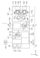
- FIG. 1 is a plan view schematically showing the configuration of a wafer processing system.
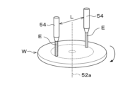
- FIG. 1 is a side view schematically showing the configuration of an etching apparatus. It is an explanatory view showing how a nozzle moves in the radial direction.
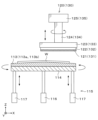
- FIG. 2 is a side view schematically showing the configuration of a grinding unit.
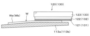
- FIG. 3 is an explanatory diagram showing how a wafer surface is ground by a grinding unit.
- FIG. 3 is a flow diagram showing the main steps of wafer processing.
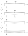
- FIG. 3 is an explanatory diagram showing the main steps of wafer processing.
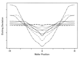
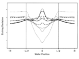
- FIG. 3 is an explanatory diagram showing an example of an etching amount deviation distribution.
- FIG. 3 is a flow diagram showing the main steps of a method for optimizing the etching amount deviation distribution.
- FIG. 3 is a flow diagram showing the main steps of wafer processing.
- FIG. 3 is a flow diagram showing the main steps of wafer processing.
- FIG. 3 is an explanatory diagram showing the main steps of wafer processing.
- FIG. 3 is a flow diagram showing the main steps of wafer processing.
- FIG. 3 is an explanatory diagram showing the main steps of wafer processing.
- FIG. 3 is a flow diagram showing the main steps of wafer processing.
- FIG. 3 is an explanatory diagram showing the main steps of wafer processing.
- FIG. 3 is an explanatory diagram showing the main steps of wafer processing.
- FIG. 3 is an explanatory diagram showing an example of an etching amount deviation distribution.
- It is an explanatory view showing an example of the shape of the 1st surface of the wafer after grinding.
- It is an explanatory view showing an example of a plurality of parts.
- the thickness of the wafer is reduced by flattening and smoothing the cut surface of a disk-shaped silicon wafer (hereinafter simply referred to as "wafer") obtained by cutting a single crystal silicon ingot using a wire saw or the like. Equalization is being done.
- the cut surface is flattened by, for example, surface grinding or lapping. Smoothening of the cut surface is performed, for example, by spin etching in which an etching solution is supplied from above the cut surface of the wafer while rotating the wafer.
- Patent Document 1 discloses that at least the front surface of a wafer obtained by slicing a semiconductor ingot is flattened by surface grinding or lapping, and then the front surface is etched by spin etching. ing.
- the spray nozzle is moved above the outer circumference of the wafer, and then the spray nozzle is positioned above the center of the wafer whose outer circumference has been etched. Fix it, supply an etching solution, and perform spin etching.
- the present inventors discovered that when the etching solution is supplied by fixing the position of the nozzle above the center of the wafer by the method disclosed in Patent Document 1, the wafer after etching is It was discovered that the surface shape could not be properly controlled. Specifically, it has been found that the amount of etching at the center of the wafer, which is directly below the discharge of the etching solution, is smaller than the amount of etching at the outer peripheral portion around the center. At the outer periphery of the wafer, the etching solution supplied to the center is passed through by centrifugal force, and etching progresses.
- a wafer W as a substrate cut out from an ingot is processed to improve the in-plane thickness uniformity.
- the cut surfaces of the wafer W will be referred to as a first surface Wa and a second surface Wb as the other surface.
- the first surface Wa is a surface opposite to the second surface Wb.
- the first surface Wa and the second surface Wb may be collectively referred to as the surface of the wafer W.
- the wafer processing system 1 has a configuration in which a loading/unloading station 10 and a processing station 11 are integrally connected.
- a cassette C capable of accommodating a plurality of wafers W is carried in and out of the carry-in/out station 10 between the cassette C and the outside.
- the processing station 11 includes various processing devices that perform desired processing on the wafer W.
- a cassette mounting table 20 is provided at the loading/unloading station 10.
- the cassette mounting table 20 is configured to be able to mount a plurality of cassettes C, for example two cassettes C, in a row in the Y-axis direction.
- the processing station 11 is provided with, for example, three processing blocks G1 to G3.
- the first processing block G1, the second processing block G2, and the third processing block G3 are arranged in this order from the X-axis negative direction side (carry-in/out station 10 side) to the positive direction side.
- the first processing block G1 is provided with reversing devices 30 and 31, a thickness measuring device 40, etching devices 50 and 51, and a wafer transport device 60.
- the reversing device 30 and the etching device 50 are arranged side by side in this order from the negative direction side of the X-axis to the positive direction side.
- the reversing devices 30, 31 and the thickness measuring device 40 are provided, for example, in a vertically stacked manner from the bottom in this order.
- the etching apparatuses 50 and 51 are stacked, for example, vertically in this order from the bottom.
- the wafer transfer device 60 is arranged on the Y-axis positive direction side of the etching devices 50 and 51. Note that the number and arrangement of the reversing devices 30 and 31, the thickness measuring device 40, the etching devices 50 and 51, and the wafer transport device 60 are not limited to these.
- the reversing devices 30 and 31 reverse the first surface Wa and the second surface Wb of the wafer W in the vertical direction.
- the configuration of the reversing devices 30 and 31 is arbitrary.
- the thickness measuring device 40 includes a measuring section (not shown) and a calculating section (not shown).
- the measurement unit includes a sensor that measures the thickness of the wafer W after grinding or etching at multiple points.
- the calculation unit acquires the thickness distribution of the wafer W from the measurement results (thickness of the wafer W) by the measurement unit, and further calculates the flatness (TTV: Total Thickness Variation) of the wafer W.
- TTV Total Thickness Variation
- Etching devices 50 and 51 etch silicon (Si) on a first surface Wa after grinding or a second surface Wb after grinding in a processing device 110, which will be described later.
- the etching apparatuses 50 and 51 include a wafer holding section 52 as a substrate holding section, a rotation mechanism 53, and a nozzle 54 as an etching liquid supply section.
- the wafer holding unit 52 holds the outer edge of the wafer W at a plurality of points, three points in this embodiment.
- the configuration of the wafer holder 52 is not limited to the illustrated example; for example, the wafer holder 52 may include a chuck that suction-holds the wafer W from below.
- the rotation mechanism 53 rotates the wafer W held by the wafer holder 52 about a vertical rotation center line 52a.
- the nozzle 54 supplies the etching liquid E to the first surface Wa or the second surface Wb of the wafer W held by the wafer holder 52.
- the nozzle 54 is connected to an etching liquid supply source (not shown) that supplies the etching liquid E to the nozzle 54 .
- the nozzle 54 is provided above the wafer holder 52 and is configured to be movable in the horizontal and vertical directions by a moving mechanism 55. In one example, the nozzle 54 is configured to be able to reciprocate (scan move) through the rotation center line 52a of the wafer holder 52, that is, over the center of the wafer W as shown in FIG.
- the etching solution E contains at least hydrofluoric acid or nitric acid in order to appropriately etch the silicon of the wafer W that can be an etching target. Further, the etching solution E may contain phosphoric acid or sulfuric acid.
- the wafer transport device 60 has, for example, two transport arms 61 that hold and transport the wafer W.
- Each transport arm 61 is configured to be movable in the horizontal direction, vertical direction, around the horizontal axis, and around the vertical axis.
- the wafer transport device 60 includes a cassette C of the cassette mounting table 20, reversing devices 30 and 31, a thickness measuring device 40, etching devices 50 and 51, a buffer device 70 described later, a cleaning device 80 described later, and a reversing device described later. 90, it is configured to be able to transport the wafer W.
- the second processing block G2 is provided with a buffer device 70, a cleaning device 80, a reversing device 90, and a wafer transport device 100.
- the buffer device 70, the cleaning device 80, and the reversing device 90 are stacked, for example, vertically in this order from the bottom.
- the wafer transfer device 100 is arranged on the Y-axis negative side of the buffer device 70, the cleaning device 80, and the reversing device 90. Note that the number and arrangement of the buffer device 70, cleaning device 80, reversing device 90, and wafer transport device 100 are not limited to these.
- the buffer device 70 temporarily holds the unprocessed wafer W transferred from the first processing block G1 to the second processing block G2.
- the configuration of the buffer device 70 is arbitrary.
- the cleaning device 80 cleans the first surface Wa or the second surface Wb after being ground by the processing device 110, which will be described later. For example, a brush is brought into contact with the first surface Wa or the second surface Wb to clean the first surface Wa or the second surface Wb. Note that a pressurized cleaning liquid may be used to clean the first surface Wa or the second surface Wb. Further, when cleaning the wafer W, the cleaning device 80 may be configured to be able to simultaneously clean the first surface Wa and the second surface Wb.
- the reversing device 90 reverses the first surface Wa and the second surface Wb of the wafer W in the vertical direction.
- the configuration of the reversing device 90 is arbitrary.
- the wafer transport device 100 has, for example, two transport arms 101 that hold and transport the wafer W.
- Each transport arm 101 is configured to be movable in the horizontal direction, vertical direction, around the horizontal axis, and around the vertical axis.
- the wafer transport device 100 is configured to be able to transport the wafer W to the etching devices 50 and 51, the buffer device 70, the cleaning device 80, the reversing device 90, and the processing device 110 described later.
- a processing device 110 is provided in the third processing block G3. Note that the number and arrangement of processing devices 110 are not limited to this.
- the processing device 110 has a rotary table 111.
- the rotary table 111 is configured to be rotatable about a vertical rotation center line 112 by a rotation mechanism (not shown).
- Four chucks 113 are provided on the rotary table 111 to hold the wafer W by suction.
- the two first chucks 113a are chucks used for grinding at the first processing position B1.
- These two first chucks 113a are arranged at point-symmetrical positions with the rotation center line 112 in between.
- the remaining two second chucks 113b are chucks used for grinding at the second processing position B2.
- These two second chucks 113b are also arranged at point-symmetrical positions with the rotation center line 112 in between. That is, the first chucks 113a and the second chucks 113b are arranged alternately in the circumferential direction.
- a porous chuck is used for the chuck 113.
- the surface of the chuck 113 that is, the holding surface of the wafer W, has a convex shape in which the center portion is more protruding than the end portions when viewed from the side.
- the protrusion at the center is minute, the protrusion at the center of the chuck 113 is illustrated in a large size in FIG. 4 for clarity of explanation.
- the chuck 113 is held on a chuck base 114.
- the chuck base 114 is provided with an inclination adjusting section 115 that adjusts the relative inclination of the chuck 113 and grinding wheels 121 and 131 included in each of the grinding units 120 and 130, which will be described later.
- the tilt adjustment unit 115 has a fixed shaft 116 provided on the lower surface of the chuck base 114 and a plurality of, for example, two, lifting shafts 117. Each lifting shaft 117 is configured to be extendable and retractable, and raises and lowers the chuck base 114.
- the inclination adjustment unit 115 allows the chuck base 114 to move up and down in the vertical direction using the lifting shaft 117 from one end (position corresponding to the fixed shaft 116) of the outer periphery of the chuck base 114 as a base point. 114 can be tilted. As a result, the relative inclination between the surfaces of the grinding wheels 121 and 131 provided in the respective grinding units 120 and 130 at processing positions B1 and B2, which will be described later, and the surface of the chuck 113 can be adjusted.
- each of the four chucks 113 can be moved to delivery positions A1 to A2 and processing positions B1 to B2 by rotating the rotary table 111. Further, each of the four chucks 113 is configured to be rotatable around a vertical axis by a rotation mechanism (not shown).
- the first transfer position A1 is a position on the negative side of the X axis and the positive side of the Y axis of the rotary table 111, and the wafer W is transferred to the first chuck 113a when grinding the first surface Wa.
- the second transfer position A2 is a position on the X-axis negative side and the Y-axis negative side of the rotary table 111, and the wafer W is transferred to the second chuck 113b when grinding the second surface Wb. .
- the first processing position B1 is a position on the X-axis positive direction side and the Y-axis negative direction side of the rotary table 111, and the first grinding unit 120 is arranged.
- the first grinding unit 120 grinds, for example, the first surface Wa or the second surface Wb of the wafer W held by the first chuck 113a.
- the second processing position B2 is a position on the X-axis positive direction side and the Y-axis positive direction side of the rotary table 111, and the second grinding unit 130 is arranged.
- the second grinding unit 130 grinds, for example, the second surface Wb or the first surface Wa of the wafer W held by the second chuck 113b.
- a thickness measuring device (not shown) for measuring the thickness of the wafer W after grinding may be provided at the delivery positions A1 and A2 or the processing positions B1 and B2.
- the first grinding unit 120 includes a grinding wheel 122 having an annular grinding wheel 121 on the lower surface, a mount 123 that supports the grinding wheel 122, and a mount 123 that rotates the grinding wheel 122 via the mount 123. It has a spindle 124 and a drive section 125 that includes, for example, a motor (not shown). Further, the first grinding unit 120 is configured to be movable in the vertical direction along a support 126 shown in FIG.
- the second grinding unit 130 has a similar configuration to the first grinding unit 120. That is, the second grinding unit 130 includes a grinding wheel 132 including an annular grinding wheel 131, a mount 133, a spindle 134, a drive section 135, and a support 136.
- the first surface Wa of the wafer W held by the first chuck 113a and the grinding wheel 121 are The first chuck 113a is tilted so that the surface forms an arbitrary angle. For example, by making the first surface Wa parallel to the surface of the grinding wheel 121, the first surface Wa after grinding can be ground flat. For example, if the surface of the grinding wheel 121 is tilted radially outward and upward with respect to the first surface Wa, the first surface Wa after grinding can be ground in a V-shape in cross-sectional view. .
- the first grinding unit 120 it is also possible to grind the first surface Wa after grinding into an A-shape, an M-shape, or a W-shape in a longitudinal cross-sectional view. Then, the annular grinding wheel 121 and the wafer W are brought into contact with each other in an arc shape from the center to the outer peripheral end, and in this state, the first chuck 113a and the grinding wheel 122 are rotated, respectively, so that the first surface Wa The entire surface is ground. The same applies when the second surface Wb is ground using the second grinding unit 130.
- the above wafer processing system 1 is provided with a control device 140 as shown in FIG.
- the control device 140 is, for example, a computer equipped with a CPU, a memory, etc., and has a program storage section (not shown).
- the program storage unit stores a program for controlling the processing of wafers W in the wafer processing system 1. Further, as described above, the control device 140 acquires the thickness distribution of the wafer W from the measurement results (thickness of the wafer W) by the thickness measuring device 40, and further includes a calculation unit (see FIG. (not shown).
- the above program may be one that has been recorded on a computer-readable storage medium H, and may have been installed in the control device 140 from the storage medium H. Further, the storage medium H may be temporary or non-temporary.
- a wafer W cut out from an ingot with a wire saw or the like and wrapped is subjected to a process to improve the in-plane thickness uniformity.
- a cassette C containing a plurality of wafers W is placed on the cassette mounting table 20 of the loading/unloading station 10.
- the wafers W are stored in the cassette C with the first surface Wa facing upward and the second surface Wb facing downward.
- the wafer W in the cassette C is taken out by the wafer transport device 60 and transported to the buffer device 70 .
- the wafer W is transported by the wafer transport device 100 to the processing device 110, and delivered to the first chuck 113a at the first delivery position A1.
- the first chuck 113a holds the second surface Wb of the wafer W by suction.
- step S101 the control device 140 controls the processing device 110 to form a concave portion War, the center of which is depressed from the outer circumference, on the first surface Wa after grinding, as shown in FIG. 7(a). , the first surface Wa is ground into a V-shape. Details of this V-shape will be described later.
- a cleaning section (not shown) may clean the first surface Wa of the wafer W after being ground.
- the wafer W is transported to the cleaning device 80 by the wafer transport device 100.
- the cleaning device 80 the first surface Wa and the second surface Wb of the wafer W are cleaned (step S102 in FIG. 6).
- the wafer W is transported to the reversing device 90 by the wafer transport device 100.
- the reversing device 90 reverses the first surface Wa and the second surface Wb of the wafer W in the vertical direction (step S103 in FIG. 6). That is, the wafer W is turned over so that the first surface Wa faces downward and the second surface Wb faces upward.
- the wafer W is transported by the wafer transport device 100 to the processing device 110, and is delivered to the second chuck 113b at the second delivery position A2.
- the second chuck 113b holds the first surface Wa of the wafer W by suction.
- step S104 the control device 140 controls the processing device 110 to form a concave portion Wbr in which the center is depressed from the outer circumference on the second surface Wb after grinding, as shown in FIG. 7(b). , the second surface Wb is ground into a V-shape. Details of this V-shape will be described later.
- the rotary table 111 is rotated to move the wafer W to the second delivery position A2.
- the second surface Wb of the wafer W after being ground may be cleaned by a cleaning section (not shown).
- the wafer W is transported to the cleaning device 80 by the wafer transport device 100.
- the cleaning device 80 the second surface Wb and the first surface Wa of the wafer W are cleaned (step S105 in FIG. 6).
- the wafer W is transported to the thickness measuring device 40 by the wafer transport device 60.
- the thickness measuring device 40 measures the thickness of the wafer W after grinding both the first surface Wa and the second surface Wb (step S106 in FIG. 6).
- the thickness of the wafer W after grinding may be measured by the thickness measuring device of the processing apparatus 110.
- the thickness measuring device 40 obtains the thickness distribution of the wafer W after grinding by measuring the thickness of the wafer W after double-sided grinding at multiple points, and further calculates the flatness of the wafer W.
- the calculated thickness distribution and flatness of the wafer W are output to the control device 140, for example.
- the control device 140 determines optimal etching conditions for subsequent etching of the first surface Wa and second surface Wb from the thickness distribution and flatness of the output wafer W, and optimizes the etching amount deviation distribution. (Step S107 in FIG. 6). A detailed method of optimizing the etching amount deviation distribution in the control device 140 will be described later.
- the etching amount deviation indicates a value (deviation) obtained by subtracting the average value of the etching amount from the etching amount within the wafer surface.
- the average value of the etching amount is a value obtained by averaging the etching amount within the wafer surface.
- the wafer W is transported to the etching device 51 by the wafer transport device 60.
- the second surface Wb of the wafer W is etched with the etching liquid E under the optimum etching conditions determined in step S107 (step S108 in FIG. 6).
- step S108 first, the wafer W is held in the wafer holding section 52 with the second surface Wb facing upward (towards the nozzle 54). Subsequently, the wafer holder 52 (wafer W) is rotated about the vertical rotation center line 52a, and the nozzle 54 starts discharging the etching liquid E to start etching the second surface Wb.
- the rotation center line 52a is used as an intermediate point for reciprocating movement (scanning). Note that a detailed method for determining etching conditions such as the rotation speed of the wafer W, the scan width of the nozzle 54, and the scan speed when reciprocating the nozzle 54 will be described later.
- the supply of the etching liquid E from the nozzle 54 is stopped, and the second surface Wb of the wafer W is rinsed with pure water and then shaken off to dry. Thereafter, the rotation of the wafer holder 52 (wafer W) is stopped, and the etching of the wafer W is completed.
- the optimal etching conditions for the wafer W are determined in step S107 based on the thickness distribution and flatness of the wafer W after grinding, as described above. Specifically, the actual measured values of the thickness distribution and flatness of the wafer W in the thickness measuring device 40, and the thickness distribution and flatness of the target surface shape of the wafer W after etching (hereinafter referred to as "target shape").
- target shape the thickness distribution and flatness of the target surface shape of the wafer W after etching
- the optimum etching conditions are determined based on the difference between
- the second surface Wb is etched under the optimum etching conditions to optimize the etching amount deviation distribution, and as shown in FIG. 7(c), the second surface Wb is shaped into the target shape. is processed flat.
- the wafer W is transported to the reversing device 31 by the wafer transport device 60.
- the reversing device 31 reverses the first surface Wa and the second surface Wb of the wafer W in the vertical direction (step S109 in FIG. 6). That is, the wafer W is turned over so that the first surface Wa faces upward and the second surface Wb faces downward.
- the wafer W is transported to the etching apparatus 50 by the wafer transport device 60.
- the etching apparatus 50 the first surface Wa of the wafer W is etched with the etching liquid E under the optimum etching conditions determined in step S107 (step S110 in FIG. 6).
- step S110 the first surface Wa is etched similarly to the second surface Wb in step S108. That is, first, the wafer W is held in the wafer holding section 52 with the first surface Wa facing upward. Subsequently, the wafer holder 52 (wafer W) is rotated, and the nozzle 54 starts discharging the etching liquid E to start etching the first surface Wa. Thereafter, while continuing to discharge the etching liquid E from the nozzle 54, the nozzle 54 is reciprocated (scanned) with the rotation center line 52a as an intermediate point, as shown in FIG. 3, to etch the first surface Wa. .
- step S110 as in step S108, the first surface Wa is etched under the optimum etching conditions to optimize the etching amount deviation distribution, and the first surface Wa is targeted as shown in FIG. 7(d).
- the shape is processed to be flat. That is, the target shape of the wafer W is flat, and the thickness distribution of the wafer W is uniform.
- the thickness measuring device 40 measures the thickness of the wafer W after etching both the first surface Wa and the second surface Wb (step S111 in FIG. 6).
- step S111 the thickness measuring device 40 measures the thickness of the wafer W after double-sided etching at a plurality of points to obtain the thickness distribution of the wafer W after etching, and further calculates the flatness of the wafer W.
- the calculated thickness distribution and flatness of the wafer W are output to, for example, the control device 140, and are used, for example, in processing another wafer W to be processed next by the wafer processing system 1.
- the wafer W that has been subjected to all the processes is transported to the cassette C of the cassette mounting table 20 by the wafer transport device 60. In this way, a series of wafer processing in the wafer processing system 1 is completed. Note that the wafer W processed by the wafer processing system 1 may be polished outside the wafer processing system 1.
- step S101 the above-described grinding of the first surface Wa (step S101), grinding of the second surface Wb (step S104), and optimization of the etching amount deviation distribution between the first surface Wa and the second surface Wb ( The detailed method of step S107) will be explained.
- step S108 while rotating the wafer W and reciprocating (scanning) the nozzle 54 in the radial direction passing through the center of the wafer W, the etching liquid E is applied from the nozzle 54 to the first surface Wa of the wafer W. is supplied to etch the first surface Wa.
- etching may be referred to as "scan etching”.
- step S110 the second surface Wb of the wafer W is scan-etched.
- the etching amount deviation distribution is optimized by adjusting etching conditions (etching recipe) such as the rotational speed (rotational speed) of the wafer W, the scanning speed in reciprocating movement of the nozzle 54, and the scanning width. .
- the horizontal axis in FIG. 8 indicates the radial position from the center of the wafer (0 (zero) on the horizontal axis) to the outer edge ( ⁇ R on the horizontal axis), and the vertical axis indicates the etching deviation (the difference from the average value of etching amount). difference).
- the wafer surface after etching tends to have an upwardly protruding A-shape.
- the shape of the wafer surface after grinding is not V-shaped, if an attempt is made to flatten the wafer surface by optimizing the etching amount deviation distribution in step S107, the desired etching amount deviation will be determined by the optimization calculation. There is a risk that the wafer surface will not be flat after etching. That is, if the shape of the wafer surface after grinding is not V-shaped, the error in optimizing the etching amount deviation distribution in step S107 may become large. Therefore, the shape of the wafer surface after grinding is preferably formed into a V-shape.
- the etching amount deviation distribution of scan etching has an upper limit on the height He of the V-shape due to the nature of the process.
- the limit height He of this etching amount deviation distribution is the difference between the maximum value and the minimum value of the etching amount deviation distribution, and is the upper limit that can be controlled in etching. For this reason, for example, when the height of the V-shaped shape on the wafer surface after grinding is large, if an attempt is made to flatten the wafer surface by optimizing the etching amount deviation distribution in step S107, the desired etching There is a possibility that the wafer surface after etching will not be flat because no amount deviation can be generated.
- the height of the V-shaped shape after grinding is large, the error in optimizing the etching amount deviation distribution in step S107 may become large. Therefore, it is preferable that the height of the V-shaped shape on the wafer surface after grinding be equal to or less than the critical height He of the etching amount deviation distribution.
- step S101 the control device 140 controls the processing device 110 to create a recess in the first surface Wa after grinding, the center of which is depressed from the outer circumference, as shown in FIG. 7(a).
- the first surface Wa is ground into a V-shape to form a War.
- the height Ha of the recessed portion War is set to be equal to or less than the critical height He of the etching amount deviation distribution. This limit height He is determined based on etching conditions, such as the supply time of the etching liquid E, the rotational speed of the wafer W, the scan speed in reciprocating movement of the nozzle 54, and the scan width. Ru.
- the critical height He is, for example, 1.0 ⁇ m or less.
- step S104 the control device 140 controls the processing device 110 to form a recess War in which the center is depressed from the outer circumference on the second surface Wb after grinding, as shown in FIG. 7(b).
- the second surface Wb is ground into a V-shape so as to form a V-shape.
- the height Hb of the recessed portion Wbr is set to be equal to or less than the critical height He of the etching amount deviation distribution.
- step S107 optimum etching conditions for subsequent etching of the first surface Wa and second surface Wb are determined from the thickness distribution and flatness of the wafer W after double-sided grinding obtained in step S106, and the etching amount is Optimize the deviation distribution.
- a plurality of parts to be used in the optimization processing described later are acquired (step S107 in FIG. 9). -0). Note that the part is the etching amount deviation distribution of the wafer W under certain etching conditions.
- step S107-0 for example, the dummy wafer is etched under a plurality of different etching conditions. Specifically, the dummy wafer is etched by changing, for example, the rotational speed of the dummy wafer during etching, the scanning speed of the nozzle 54, or the scanning width of the nozzle 54 (see scan width L in FIG. 3). At this time, the etching time for each dummy wafer is the same.
- the etching of the dummy wafer is performed by rotating the dummy wafer and reciprocating the nozzle 54 while supplying the etching liquid E from the nozzle 54 to the dummy wafer, similar to the etching in steps S108 and S110.
- the reciprocating movement of the nozzle 54 between both ends of the dummy wafer is defined as one loop.
- Etching of the dummy wafer under each etching condition is performed for a predetermined desired time (desired number of loops). Then, the etching amount deviation distribution of the dummy wafer is acquired, and the etching amount deviation distribution is output to the control device 140. Furthermore, the control device 140 compresses the outputted etching amount deviation distribution under each etching condition into an etching amount deviation distribution per unit time (unit number of loops), and applies each compressed etching amount deviation distribution to the above-mentioned parts. be memorized as .
- FIG. 10 shows an example of multiple parts.
- the horizontal axis in FIG. 10 indicates the radial position from the center of the wafer (0 (zero) on the horizontal axis) to the outer edge ( ⁇ R on the horizontal axis), and the vertical axis indicates the etching deviation.
- the example shown in FIG. 10 is a case where a total of 36 types of parts are stored in the control device 140, or in other words, an example where etching amount deviation distributions are obtained under a total of 36 types of different etching conditions.
- the unit time (unit number of loops) can be set arbitrarily depending on the purpose, but in order to properly obtain the target etching amount deviation distribution in the overlapping of parts described later, the unit time (unit number of loops) should be set as desired. Short is preferable.
- the unit time of a part stored in the control device 140 is the time for one loop (one round trip of the scan width L shown in FIG. 3), preferably 0.5 loops (one round trip of the scan width L shown in FIG. 3). It can take a half round trip) minutes.
- the object to be etched when obtaining parts is not limited to the dummy wafer.
- the etching process result of the wafer W actually processed in the wafer processing system 1 may be stored as the above-mentioned part.
- optimal etching conditions are determined using the plurality of parts (FIG. 10) acquired in this way.
- the steps described above are performed.
- the target etching amount deviation distribution in the etching processes of S108 and S110 is obtained (step S107-1 in FIG. 9).
- the target shapes of the first surface Wa and the second surface Wb are each flat.
- the target etching amount deviation distributions of the first surface Wa and the second surface Wb are each calculated by calculating the average value of the difference between the thickness distribution of the target shape and the thickness distribution of the measured shape of the wafer W, for example. It can be obtained by dividing the subtracted value in half.
- the target etching amount deviation distributions of the first surface Wa and the second surface Wb each have a V-shape as shown in FIG.
- step S107-2 in FIG. 9).
- step S107-2 for example, the control of the etching amount deviation distribution is applied to the knapsack problem to optimize the number of overlapping parts.
- the etching amount deviation distribution is the knapsack problem, and the parts are the items that are the knapsack problem. Then, the number of times the parts are stacked is optimized so that the difference between the stacked etching amount deviation distribution and the target etching amount deviation distribution is minimized.
- a genetic algorithm or dynamic programming can be used. Then, by executing optimization calculation, one or more parts to be used for superposition are selected from the plurality of parts shown in FIG. 10 as shown in FIG. 111, and the selected parts are further selected as shown in FIG. 12. Overlap. Then, the superimposed etching amount deviation distribution (solid line in FIG. 12) approximates the target etching amount deviation distribution (broken line in FIG. 12).
- the number of times the parts are overlapped is optimized so that the time required to supply the etching liquid E from the nozzle 54 to the wafer W in the etching process is minimized.
- so-called multi-objective optimization is performed in which both the etching amount deviation distribution, that is, the etching accuracy, and the supply time of the etching liquid E are optimized.
- the optimization is performed using the following formula (1).
- the etching accuracy is the accuracy of the etching amount deviation distribution within the wafer surface.
- step S107-2 the loss function of the etching amount deviation distribution (etching accuracy) is calculated by the weighted linear sum of the flatness of the measured shape and the variation in the thickness distribution of the measured shape. do.
- the coefficient ⁇ is 0.5
- the flatness (TTV) and the thickness distribution variation (RMSE) have the same weight.
- the coefficient ⁇ is 1, the algorithm places emphasis on flatness, and when the coefficient ⁇ is 0 (zero), the algorithm places emphasis on variations in thickness distribution.
- step S107-2 when optimizing the number of overlapping parts, the number of overlapping may be optimized in units of 0.5 loops. In such a case, for example, it becomes possible to start and end the supply of the etching liquid E from the center of the wafer W.
- the etching conditions corresponding to the parts optimized in step S107-2 are integrated to determine the optimal etching conditions (step S107 in FIG. 9). -3).
- the optimum etching conditions are determined by integrating the plurality of etching conditions so that the selected etching conditions are repeated an optimized number of times.
- the optimum etching conditions include, for example, the rotation speed of the wafer W during etching, the scan speed of the nozzle 54, the scan width of the nozzle 54, and the like.
- the optimum etching conditions for the first surface Wa and the second surface Wb are determined, and the etching amount deviation distribution between the first surface Wa and the second surface Wb is optimized.
- the first surface Wa and the second surface Wb are ground into a V-shape in steps S101 and S104, and the heights Ha and Hb of the recesses War and Wbr are set as the limits of the etching amount deviation distribution.
- the height should be less than He.
- step S107 optimum etching conditions for the subsequent etching process of the first surface Wa and the second surface Wb are determined from the thickness distribution and flatness of the wafer W after double-sided grinding obtained in step S106. , the etching amount deviation distribution can be optimized.
- step S107 an optimization method is used to optimize the parts to be superimposed and the number of times the parts are superimposed to determine the optimum etching conditions.
- the first surface is Wa and the second surface Wb can be etched.
- the etching amount deviation distribution in the etching process can be brought close to the target etching amount deviation distribution, and as a result, the surface shape of the wafer W after etching can be made into the target shape.
- optimal etching conditions can be determined from undefined etching conditions, and the surface shape of the wafer W after etching can be appropriately controlled.
- steps S101 to S111 are performed for each wafer W, the surface shape of the wafer W after etching can be controlled individually.
- step S107 optimum etching conditions for the subsequent etching process of the first surface Wa and the second surface Wb are determined from the thickness distribution and flatness of the wafer W after double-sided grinding acquired in step S106. was determined and the etching amount deviation distribution was optimized.
- the thickness distribution and flatness of the wafer W may be obtained each time before optimizing the etching amount deviation distribution between the first surface Wa and the second surface Wb.
- steps S201 to S206 are performed to perform double-sided grinding, double-sided cleaning, and thickness measurement. These steps S201 to S206 are similar to steps S101 to S106 of the above embodiment.
- steps S201 and S204 the first surface Wa and the second surface Wb are ground into a V-shape as shown in FIGS. 7(a) and 7(b).
- step S207 the optimum etching conditions for the second surface Wb are determined from the thickness distribution and flatness of the wafer W obtained in step S206, and after optimizing the etching amount deviation distribution of the second surface Wb,
- step S208 the second surface Wb is etched under the optimum etching conditions as shown in FIG. 7(c).
- steps S207 and S208 are similar to steps S107 and S108 in the above embodiment.
- step S209 the first surface Wa and the second surface Wb are reversed. This step S209 is similar to step S109 in the above embodiment.
- step S210 the thickness of the wafer W is measured at multiple points to obtain the thickness distribution of the wafer W after grinding, and further the flatness of the wafer W is calculated. Then, in step S211, the optimum etching conditions for the first surface Wa are determined from the thickness distribution and flatness of the wafer W to optimize the etching amount deviation distribution of the first surface Wa. The first surface Wa is etched under the following conditions.
- step S213 the thickness of the wafer W is measured at multiple points to obtain the thickness distribution of the wafer W after grinding, and further the flatness of the wafer W is calculated.
- This step S213 is similar to step S111 in the above embodiment.
- the first surface Wa and the second surface Wb can be precisely etched.
- the etching amount deviation distribution on both sides is optimized.
- optimization of the grinding shape of the wafer W and the etching amount deviation distribution It may be.
- the etching amount deviation distribution on only one side may be optimized.
- Steps S301 to S305 are performed to perform double-sided grinding and double-sided cleaning. These steps S301 to S305 are similar to steps S101 to S105 in the above embodiment.
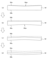
- step S301 as shown in FIG. 15(a), the first surface Wa after grinding is shaped into a V-shape so as to form a concave portion War whose center is depressed from the outer circumference. Grind.
- step S304 as shown in FIG. 15(b), the second surface Wb after grinding is shaped into a V-shape so as to form a recess Wbr in which the center is depressed from the outer circumference. Grind.
- step S306 the second surface Wb is etched, as shown in FIG. 15(c). At this time, the etching amount deviation of the second surface Wb is uniform within the surface, that is, the etching amount deviation distribution is uniform. After that, in step S307, the first surface Wa and the second surface Wb are reversed. This step S307 is similar to step S109 in the above embodiment.
- step S308 the thickness of the wafer W is measured at multiple points to obtain the thickness distribution of the wafer W after grinding, and further the flatness of the wafer W is calculated.
- step S309 optimum etching conditions for etching the first surface Wa are determined from the thickness distribution and flatness of the wafer W acquired in step S308, and the etching amount deviation distribution is optimized.
- step S310 as shown in FIG. 15(d), the first surface Wa is etched under the optimal etching conditions determined in step S309. That is, in this embodiment after etching, the thickness distribution of the wafer W becomes uniform.
- This step S310 is similar to step S110 in the above embodiment.
- step S311 the thickness of the wafer W is measured at multiple points to obtain the thickness distribution of the wafer W after grinding, and further the flatness of the wafer W is calculated.
- step S311 is similar to step S111 in the above embodiment.
- steps S301 to S311 are performed continuously on a plurality of wafers W
- the etching amount deviation of the second surface Wb is uniform within the surface in step S306.
- the second surfaces Wb of a plurality of wafers W are etched under the same etching conditions.
- one side of the wafer W may be ground into a V-shape and the other side may be ground flat, and then the etching amount deviation distribution on both sides may be optimized.
- Steps S401 to S406 are performed to perform double-sided grinding, double-sided cleaning, and thickness measurement. These steps S401 to S406 are similar to steps S101 to S106 of the above embodiment, but the second surface Wb is ground flat.
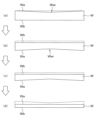
- step S401 as shown in FIG. 17(a), the first surface Wa after grinding is shaped into a V-shape so as to form a concave portion War whose center is depressed from the outer circumference. Grind.
- the second surface Wb is ground flat as shown in FIG. 17(b).
- step S407 the optimum etching conditions for the etching process of the second surface Wb are determined from the thickness distribution and flatness of the wafer W after double-sided grinding obtained in step S406, and the etching amount deviation distribution is optimized.
- This step S407 is similar to step S107 in the above embodiment.
- step S408 as shown in FIG. 17(c), the second surface Wb is etched under the optimal etching conditions determined in step S407. After that, in step S409, the first surface Wa and the second surface Wb are reversed. These steps S408 and S409 are similar to steps S108 and S109 in the above embodiment.
- step S410 the thickness of the wafer W is measured at multiple points to obtain the thickness distribution of the wafer W after grinding, and further the flatness of the wafer W is calculated.
- step S411 optimum etching conditions for etching the first surface Wa are determined from the thickness distribution and flatness of the wafer W acquired in step S410, and the etching amount deviation distribution is optimized.
- step S412 as shown in FIG. 17(d), the first surface Wa is etched under the optimal etching conditions determined in step S411. That is, in this embodiment after etching, the thickness distribution of the wafer W becomes uniform.
- step S412 is similar to step S110 in the above embodiment.
- step S413 the thickness of the wafer W is measured at multiple points to obtain the thickness distribution of the wafer W after grinding, and further the flatness of the wafer W is calculated.
- This step S413 is similar to step S111 in the above embodiment.
- one side of the wafer W may be ground into a V-shape and the other side may be ground flat, and then the etching amount deviation distribution of only one side may be optimized.
- Steps S501 to S505 are performed to perform double-sided grinding and double-sided cleaning. These steps S501 to S505 are similar to steps S101 to S105 of the above embodiment, but the second surface Wb is ground flat.
- step S501 as shown in FIG. 19(a), the first surface Wa after grinding is shaped into a V-shape so that the center part forms a concave part War that is depressed from the outer peripheral part. Grind.
- the second surface Wb is ground flat as shown in FIG. 19(b).
- step S506 the second surface Wb is etched as shown in FIG. 19(c). At this time, the etching amount deviation of the second surface Wb is uniform within the surface, that is, the etching amount deviation distribution is uniform. After that, in step S307, the first surface Wa and the second surface Wb are reversed. This step S507 is similar to step S109 in the above embodiment.
- step S508 the thickness of the wafer W is measured at multiple points to obtain the thickness distribution of the wafer W after grinding, and further the flatness of the wafer W is calculated.
- step S509 optimum etching conditions for etching the first surface Wa are determined from the thickness distribution and flatness of the wafer W acquired in step S508, and the etching amount deviation distribution is optimized.
- step S510 as shown in FIG. 19(d), the first surface Wa is etched under the optimal etching conditions determined in step S509. That is, in this embodiment after etching, the thickness distribution of the wafer W becomes uniform.
- This step S310 is similar to step S110 in the above embodiment.
- step S511 the thickness of the wafer W is measured at multiple points to obtain the thickness distribution of the wafer W after grinding, and further the flatness of the wafer W is calculated.
- step S511 is similar to step S111 in the above embodiment.
- steps S501 to S511 are performed continuously on a plurality of wafers W
- the etching amount deviation of the second surface Wb is uniform within the surface in step S506.
- the second surfaces Wb of a plurality of wafers W are etched under the same etching conditions.
- the shape can be controlled up to the outermost periphery of the surface of the wafer W.
- the scan etching in steps S108 and S110 in order to prevent the etching solution E from splashing, the etching amount deviation distribution can be controlled only in the area inside the scan width L as shown in FIG. In some regions, the etching amount deviation distribution becomes flat and cannot be controlled. In such a case, the error in optimizing the etching amount deviation distribution in step S107 may become large.
- step S101 on the first surface Wa after grinding, a recessed part War whose center part is depressed from the outer peripheral part and a flat part Waf provided around the recessed part War are formed.
- the recess War has a V-shape in cross-sectional view, and is formed in a circular shape having the same center as the first surface Wa in plan view.
- the diameter D of the recessed portion War is less than or equal to the scan width L.
- the flat portion Waf is formed in an annular shape having the same center as the first surface Wa in a plan view. Note that the boundary point between the concave portion War and the flat portion Waf is determined, for example, according to the inflection point of grinding in the processing device 110.
- the second surface Wb after grinding may be formed with a recess Wbr whose center is depressed from the outer circumference and a flat part Wbf provided around the recess Wbr. .
- step S107 When optimizing the etching amount deviation distribution of the first surface Wa in step S107, a plurality of parts shown in FIG. 22 are acquired in step S107-0.
- the subsequent target etching amount deviation distribution in step S107-1, optimization of parts and number of overlaps in step S107-2, and determination of optimal etching conditions in step S107-3 are the same as in the above embodiment.
- the first surface Wa and the second surface Wb in steps S108 and S110 are The accuracy of optimizing the etching amount deviation distribution of the surface Wb can be further improved.
- the processing apparatus 110 may have two types of grinding units (grinding shafts).
- the second grinding unit 130 grinds around the center of the first surface Wa to form the recess War. form.
- the etching process on the first surface Wa and the second surface Wb of the wafer W is performed using an etching amount deviation distribution (a distribution of the value obtained by subtracting the average value of the etching amount from the etching amount within the wafer surface). ), but it may be controlled based on the distribution of the etching amount (absolute value). For example, by optimizing the etching amount deviation distribution, the shape (profile) of the wafer W after etching can be precisely controlled, and by optimizing the etching amount, the shape of the wafer W after etching can be precisely controlled. At the same time, the thickness of the wafer W can be precisely controlled.
- the shape of the wafer W can be controlled more precisely based on the etching amount deviation distribution than on the basis of the etching amount. Therefore, if it is desired to control the shape of the wafer W more precisely, it is preferable to select control based on the etching amount deviation distribution. When it is desired to precisely control the thickness of the wafer W in accordance with the shape of the wafer W, it is preferable to control the thickness based on the etching amount. Furthermore, in the etching process for the first surface Wa and the second surface Wb of the wafer W, control based on the etching amount may be combined.
- various treatments are performed on a wafer W cut out from an ingot by a wire saw or the like and wrapped.
- the technology of this disclosure can be applied. Specifically, for example, in a polymerized wafer formed by bonding a first wafer and a second wafer, even when etching the surface of the first wafer after grinding the first wafer. , the technology of the present disclosure can be applied.
Landscapes
- Mechanical Treatment Of Semiconductor (AREA)
- Weting (AREA)
Abstract
Description

40 厚み測定装置
50、51 エッチング装置
54 ノズル
110 加工装置
140 制御装置
W ウェハ
War 凹部
Claims (19)
- 基板を処理する基板処理方法であって、
前記基板の一面を研削して、前記一面の中心部が外周部より窪んだ凹部を形成することと、
研削後の前記基板の厚みを測定して、当該基板の厚み分布を取得することと、
前記厚み分布に基づいて、前記一面をエッチングする際のエッチング量偏差分布を最適化する最適エッチング条件を算出することと、
前記最適エッチング条件に基づいて、研削後の前記基板の前記一面にエッチング液供給部からエッチング液を供給して当該一面をエッチングすることと、を含む、基板処理方法。 - 前記凹部の高さは、前記一面をエッチングする際に制御可能な前記エッチング量偏差分布の最大値と最小値の差分以下である、請求項1に記載の基板処理方法。
- 前記差分は、前記一面のエッチング条件に基づいて決定される、請求項2に記載の基板処理方法。
- 前記差分は1.0μm以下である、請求項3に記載の基板処理方法。
- 研削後の前記一面には、前記凹部と、当該凹部の周囲に環状に設けられた平坦部とが形成され、
前記凹部の径は、前記エッチング液供給部を前記一面の中心部を通る径方向に往復移動させる際のスキャン幅以下である、請求項1~4のいずれか一項に記載の基板処理方法。 - 前記一面を研削することは、
前記一面を平坦に研削することと、
平坦に研削された前記一面の中心部周辺を更に研削して前記凹部を形成することと、を含む、請求項5に記載の基板処理方法。 - 前記エッチング量偏差分布の最適化は、前記基板を回転させる際の回転速度、前記エッチング液供給部を往復移動させる際のスキャン速度、及び前記エッチング液供給部を往復移動させる際のスキャン幅の少なくともいずれかに基づいて行われる、請求項1又は2に記載の基板処理方法。
- 前記エッチング量偏差分布を最適化することは、
複数の異なるエッチング条件で前記一面をエッチングした際の、当該一面のエッチング量偏差分布を取得することと、
最適化手法を用いて、前記複数のエッチング条件に対応する前記エッチング量偏差分布を重ね合わせて、前記一面の形状が目標形状になるように、重ね合わせに用いる前記エッチング量偏差分布と、当該エッチング量偏差分布を重ね合わせる回数との組み合わせを最適化することと、を含む、請求項1又は2に記載の基板処理方法。 - 前記一面のエッチングの前に、前記基板の他面を研削する、請求項1又は2に記載の基板処理方法。
- 前記厚み分布に基づいて、前記他面をエッチングする際のエッチング量偏差分布を最適化する他の最適エッチング条件を算出することと、
前記他の最適エッチング条件に基づいて、研削後の前記他面をエッチングすることと、を含む、請求項9に記載の基板処理方法。 - 前記一面のエッチングの前に、前記基板の他面を研削して、前記他面の中心部が外周部より窪んだ凹部を形成する、請求項1又は2に記載の基板処理方法。
- 前記一面のエッチングの前に、前記基板の他面を研削することを含み、
前記他面の研削と前記一面の研削を複数の基板に対して連続して行い、
前記他面の研削は、前記複数の基板に対して同じエッチング条件で行う、請求項1又は2に記載の基板処理方法。 - 基板を処理する基板処理システムであって、
前記基板の一面を研削して、前記一面の中心部が外周部より窪んだ凹部を形成する加工装置と、
前記基板の厚みを測定する厚み測定装置と、
前記一面にエッチング液供給部からエッチング液を供給して当該一面をエッチングするエッチング装置と、
制御装置と、を有し、
前記制御装置は、
研削後に前記厚み測定装置で測定された前記基板の厚みから、当該基板の厚み分布を取得することと、
前記厚み分布に基づいて、前記一面をエッチングする際のエッチング量偏差分布を最適化する最適エッチング条件を算出することと、
前記エッチング装置を用いて、前記最適エッチング条件に基づいて前記一面をエッチングさせることと、を実行する、基板処理システム。 - 前記制御装置は、前記凹部の高さを、前記一面をエッチングする際に制御可能な前記エッチング量偏差分布の最大値と最小値の差分以下に制御する、請求項13に記載の基板処理システム。
- 前記制御装置は、前記差分を、前記一面のエッチング条件に基づいて決定する、請求項14に記載の基板処理システム。
- 前記制御装置は、
前記加工装置を用いて、研削後の前記一面に、前記凹部と、当該凹部の周囲に環状に設けられた平坦部とを形成する制御を行い、
前記凹部の径を、前記エッチング液供給部を前記一面の中心部を通る径方向に往復移動させる際のスキャン幅以下にする、請求項13~15のいずれか一項に記載の基板処理システム。 - 前記制御装置は、前記加工装置を用いて、
前記一面を平坦に研削する制御を行うことと、
平坦に研削された前記一面の中心部周辺を更に研削して前記凹部を形成する制御を行うことと、を実行する、請求項16に記載の基板処理システム。 - 前記制御装置は、前記エッチング量偏差分布の最適化を、前記基板を回転させる際の回転速度、前記エッチング液供給部を往復移動させる際のスキャン速度、及び前記エッチング液供給部を往復移動させる際のスキャン幅の少なくともいずれかに基づいて行う、請求項13又は14に記載の基板処理システム。
- 前記制御装置は、
前記エッチング量偏差分布を最適化する際に、
複数の異なるエッチング条件で前記一面をエッチングした際の、当該一面のエッチング量偏差分布を取得することと、
最適化手法を用いて、前記複数のエッチング条件に対応する前記エッチング量偏差分布を重ね合わせて、前記一面の形状が目標形状になるように、重ね合わせに用いる前記エッチング量偏差分布と、当該エッチング量偏差分布を重ね合わせる回数との組み合わせを最適化することと、実行する、請求項13又は14に記載の基板処理システム。
Priority Applications (4)
| Application Number | Priority Date | Filing Date | Title |
|---|---|---|---|
| CN202380037482.5A CN119137711A (zh) | 2022-05-13 | 2023-05-01 | 基板处理方法和基板处理系统 |
| US18/864,999 US20250316506A1 (en) | 2022-05-13 | 2023-05-01 | Substrate processing method and substrate processing system |
| JP2024520419A JPWO2023219026A1 (ja) | 2022-05-13 | 2023-05-01 | |
| KR1020247040196A KR20250011637A (ko) | 2022-05-13 | 2023-05-01 | 기판 처리 방법 및 기판 처리 시스템 |
Applications Claiming Priority (2)
| Application Number | Priority Date | Filing Date | Title |
|---|---|---|---|
| JP2022079719 | 2022-05-13 | ||
| JP2022-079719 | 2022-05-13 |
Publications (1)
| Publication Number | Publication Date |
|---|---|
| WO2023219026A1 true WO2023219026A1 (ja) | 2023-11-16 |
Family
ID=88730441
Family Applications (1)
| Application Number | Title | Priority Date | Filing Date |
|---|---|---|---|
| PCT/JP2023/017025 Ceased WO2023219026A1 (ja) | 2022-05-13 | 2023-05-01 | 基板処理方法及び基板処理システム |
Country Status (6)
| Country | Link |
|---|---|
| US (1) | US20250316506A1 (ja) |
| JP (1) | JPWO2023219026A1 (ja) |
| KR (1) | KR20250011637A (ja) |
| CN (1) | CN119137711A (ja) |
| TW (1) | TW202422668A (ja) |
| WO (1) | WO2023219026A1 (ja) |
Cited By (2)
| Publication number | Priority date | Publication date | Assignee | Title |
|---|---|---|---|---|
| WO2025197673A1 (ja) * | 2024-03-22 | 2025-09-25 | 東京エレクトロン株式会社 | 基板処理方法、基板処理装置及びコンピュータ記憶媒体 |
| WO2025263366A1 (ja) * | 2024-06-21 | 2025-12-26 | 東京エレクトロン株式会社 | 基板処理方法、基板処理システム及びパラメータの補正方法 |
Citations (4)
| Publication number | Priority date | Publication date | Assignee | Title |
|---|---|---|---|---|
| US5821166A (en) * | 1996-12-12 | 1998-10-13 | Komatsu Electronic Metals Co., Ltd. | Method of manufacturing semiconductor wafers |
| JP2014127618A (ja) * | 2012-12-27 | 2014-07-07 | Disco Abrasive Syst Ltd | 板状物の加工方法 |
| JP2017188549A (ja) * | 2016-04-05 | 2017-10-12 | 三益半導体工業株式会社 | スピンエッチング方法及び装置並びに半導体ウェーハの製造方法 |
| JP2021034533A (ja) * | 2019-08-23 | 2021-03-01 | 東京エレクトロン株式会社 | 基板処理方法及び基板処理システム |
Family Cites Families (1)
| Publication number | Priority date | Publication date | Assignee | Title |
|---|---|---|---|---|
| JPH11135464A (ja) | 1997-10-30 | 1999-05-21 | Komatsu Electron Metals Co Ltd | 半導体ウェハの製造方法 |
-
2023
- 2023-05-01 JP JP2024520419A patent/JPWO2023219026A1/ja active Pending
- 2023-05-01 WO PCT/JP2023/017025 patent/WO2023219026A1/ja not_active Ceased
- 2023-05-01 KR KR1020247040196A patent/KR20250011637A/ko active Pending
- 2023-05-01 US US18/864,999 patent/US20250316506A1/en active Pending
- 2023-05-01 CN CN202380037482.5A patent/CN119137711A/zh active Pending
- 2023-05-03 TW TW112116357A patent/TW202422668A/zh unknown
Patent Citations (4)
| Publication number | Priority date | Publication date | Assignee | Title |
|---|---|---|---|---|
| US5821166A (en) * | 1996-12-12 | 1998-10-13 | Komatsu Electronic Metals Co., Ltd. | Method of manufacturing semiconductor wafers |
| JP2014127618A (ja) * | 2012-12-27 | 2014-07-07 | Disco Abrasive Syst Ltd | 板状物の加工方法 |
| JP2017188549A (ja) * | 2016-04-05 | 2017-10-12 | 三益半導体工業株式会社 | スピンエッチング方法及び装置並びに半導体ウェーハの製造方法 |
| JP2021034533A (ja) * | 2019-08-23 | 2021-03-01 | 東京エレクトロン株式会社 | 基板処理方法及び基板処理システム |
Cited By (2)
| Publication number | Priority date | Publication date | Assignee | Title |
|---|---|---|---|---|
| WO2025197673A1 (ja) * | 2024-03-22 | 2025-09-25 | 東京エレクトロン株式会社 | 基板処理方法、基板処理装置及びコンピュータ記憶媒体 |
| WO2025263366A1 (ja) * | 2024-06-21 | 2025-12-26 | 東京エレクトロン株式会社 | 基板処理方法、基板処理システム及びパラメータの補正方法 |
Also Published As
| Publication number | Publication date |
|---|---|
| KR20250011637A (ko) | 2025-01-21 |
| CN119137711A (zh) | 2024-12-13 |
| TW202422668A (zh) | 2024-06-01 |
| US20250316506A1 (en) | 2025-10-09 |
| JPWO2023219026A1 (ja) | 2023-11-16 |
Similar Documents
| Publication | Publication Date | Title |
|---|---|---|
| WO2023219026A1 (ja) | 基板処理方法及び基板処理システム | |
| JP7703668B2 (ja) | 基板処理方法及び基板処理システム | |
| JP2025120456A (ja) | 基板処理方法、基板処理システム及びプログラム | |
| JP7804529B2 (ja) | 基板処理方法及び基板処理システム | |
| JP7716483B2 (ja) | 基板処理方法及び基板処理システム | |
| US20240290607A1 (en) | Substrate processing method, substrate processing system and computer-readable recording medium | |
| WO2024214536A1 (ja) | 基板処理方法及び基板処理システム | |
| WO2025041580A1 (ja) | 基板処理方法及び基板処理システム | |
| TWI916586B (zh) | 基板處理方法及基板處理系統 | |
| WO2025089152A1 (ja) | 基板処理方法及び基板処理システム | |
| WO2025047459A1 (ja) | 基板処理方法及び基板処理システム | |
| CN118103956A (zh) | 基板处理方法和基板处理系统 | |
| TW202603873A (zh) | 基板處理方法、基板處理裝置及電腦記錄媒體 | |
| WO2025263366A1 (ja) | 基板処理方法、基板処理システム及びパラメータの補正方法 | |
| JP2022159931A (ja) | 基板処理方法及び基板処理システム | |
| WO2025263345A1 (ja) | 最適厚み測定位置を決定する方法、基板処理方法及び基板処理装置 | |
| TW202529195A (zh) | 基板處理方法及基板處理系統 | |
| TW202506332A (zh) | 研磨裝置、傾斜調整方法及資訊顯示部 | |
| WO2025229869A1 (ja) | 基板処理方法、基板処理装置及びコンピュータ記憶媒体 | |
| KR20260056205A (ko) | 기판 처리 방법 및 기판 처리 시스템 |
Legal Events
| Date | Code | Title | Description |
|---|---|---|---|
| 121 | Ep: the epo has been informed by wipo that ep was designated in this application |
Ref document number: 23803503 Country of ref document: EP Kind code of ref document: A1 |
|
| WWE | Wipo information: entry into national phase |
Ref document number: 202380037482.5 Country of ref document: CN |
|
| WWE | Wipo information: entry into national phase |
Ref document number: 2024520419 Country of ref document: JP |
|
| WWE | Wipo information: entry into national phase |
Ref document number: 18864999 Country of ref document: US |
|
| ENP | Entry into the national phase |
Ref document number: 20247040196 Country of ref document: KR Kind code of ref document: A |
|
| WWE | Wipo information: entry into national phase |
Ref document number: 1020247040196 Country of ref document: KR |
|
| NENP | Non-entry into the national phase |
Ref country code: DE |
|
| 122 | Ep: pct application non-entry in european phase |
Ref document number: 23803503 Country of ref document: EP Kind code of ref document: A1 |
|
| WWP | Wipo information: published in national office |
Ref document number: 18864999 Country of ref document: US |